

Sony HCD-300 Schematic

HCD-S300
SERVICE MANUAL
HCD-S300 is the amplifier, DVD/CD and
tuner section in DAV-S300.
Model Name Using Similar Mechanism NEW
Mechanism Type CDM-55D-DVBU2
Base Unit Type DVBU2
Optical Pick-up Type KHM220AAA/CINP1
SPECIFICATIONS
US Model
AEP Model
UK Model
E Model
Australian Model
Chinese Model
MICROFILM
COMPACT AV SYSTEM
1

Laser component in this product is capable of emitting radiation
exceeding the limit for Class 1.
This appliance is classified as
a CLASS 1 LASER product.
The CLASS 1 LASER PRODUCT MARKING is located on
the rear exterior.
This caution
label is located
inside the unit.
SAFETY CHECK-OUT
After correcting the original service problem, perform the following safety checks before releasing the set to the customer:
Check the antenna terminals, metal trim, “metallized” knobs, screws,
and all other exposed metal parts for AC leakage. Check leakage as
described below.
LEAKAGE
The AC leakage from any exposed metal part to earth Ground and
from all exposed metal parts to any exposed metal part having a
return to chassis, must not exceed 0.5 mA (500 microampers). Leakage current can be measured by any one of three methods.
1. A commercial leakage tester, such as the Simpson 229 or RCA
WT-540A. Follow the manufacturers’ instructions to use these
instruments.
2. A battery-operated AC milliammeter. The Data Precision 245
digital multimeter is suitable for this job.
3. Measuring the voltage drop across a resistor by means of a VOM
or battery-operated AC voltmeter. The “limit” indication is 0.75
V, so analog meters must have an accurate low-voltage scale.
The Simpson 250 and Sanwa SH-63Trd are examples of a passive VOM that is suitable. Nearly all battery operated digital
multimeters that have a 2V AC range are suitable. (See Fig. A)
To Exposed Metal
Parts on Set
CAUTION
Use of controls or adjustments or performance of procedures
other than those specified herein may result in hazardous radiation exposure.
Notes on chip component replacement
• Never reuse a disconnected chip component.
• Notice that the minus side of a tantalum capacitor may be
damaged by heat.
Flexible Circuit Board Repairing
• Keep the temperature of soldering iron around 270˚C
during repairing.
• Do not touch the soldering iron on the same conductor of the
circuit board (within 3 times).
• Be careful not to apply force on the conductor when soldering
or unsoldering.
SAFETY-RELATED COMPONENT WARNING !!
0.15µF
1.5kΩ
Earth Ground
AC
voltmeter
(0.75V)
Fig. A. Using an AC voltmeter to check AC leakage.
COMPONENTS IDENTIFIED BY MARK 0 OR DOTTED LINE
WITH MARK 0 ON THE SCHEMATIC DIAGRAMS AND IN
THE PARTS LIST ARE CRITICAL TO SAFE OPERATION.
REPLACE THESE COMPONENTS WITH SONY PARTS
WHOSE PART NUMBERS APPEAR AS SHOWN IN THIS
MANUAL OR IN SUPPLEMENTS PUBLISHED BY SONY.
2

TABLE OF CONTENTS
1. SERVICING NOTE .......................................................... 4
2. GENERAL ..........................................................................5
3. DISASSEMBLY
3-1. Loading Panel ...................................................................... 6
3-2. Front Panel ........................................................................... 6
3-3. CD Mechanism .................................................................... 7
3-4. Disc Tray .............................................................................. 7
4. TEST MODE ....................................................................... 8
5. ELECTRICAL ADJUSTMENT ................................. 18
6. DIAGRAMS
6-1. Circuit Boards Location ..................................................... 19
6-2. Block Diagrams ................................................................. 21
• RF/Servo Section ............................................................ 21
• Main Section ...................................................................22
• Signal Process/Video Section ......................................... 23
• Audio Main Section........................................................24
• I/O, Tuner Section .......................................................... 25
• AMP Section...................................................................26
• Display Section ...............................................................26
• Power Section ................................................................. 27
6-3. Printed Wiring Board – TK Section –................................28
6-4. Schematic Diagram – TK Section – .................................. 29
6-5. Printed Wiring Board – DVD Section – ............................30
6-6. Schematic Diagram – DVD (1/12) Section – .................... 32
6-7. Schematic Diagram – DVD (2/12) Section – .................... 33
6-8. Schematic Diagram – DVD (3/12) Section – .................... 34
6-9. Schematic Diagram – DVD (4/12) Section – .................... 35
6-10.Schematic Diagram – DVD (5/12) Section – ....................36
6-11.Schematic Diagram – DVD (6/12) Section – ....................37
6-12.Schematic Diagram – DVD (7/12) Section – ....................38
6-13.Schematic Diagram – DVD (8/12) Section – ....................39
6-14.Schematic Diagram – DVD (9/12) Section – ....................40
6-15.Schematic Diagram – DVD (10/12) Section – ..................41
6-16.Schematic Diagram – DVD (11/12) Section – ..................42
6-17.Schematic Diagram – DVD (12/12) Section – ..................43
6-18. Schematic Diagram – FRONT (1/2) Section – .................44
6-19. Printed Wiring Board – FRONT (1/2) Section – .............. 45
6-20. Schematic Diagram – FRONT (2/2) Section – .................46
6-21. Printed Wiring Board – FRONT (2/2) Section – .............. 47
6-22. Schematic Diagram – VIDEO Section –........................... 48
6-23.Printed Wiring Board – VIDEO Section –......................... 49
6-24.Schematic Diagram – AUDIO Section – ........................... 50
6-25.Printed Wiring Board – AUDIO Section – ........................ 51
6-26.Schematic Diagram – PROTECT Section – ...................... 52
6-27.Printed Wiring Board – PROTECT Section – ................... 53
6-28.Printed Wiring Board – POWER (US only) Section – ...... 54
6-29.Printed Wiring Board
– POWER (AEP, UK, SP, HK, E32, AUS only) Section – .. 56
6-30.Schematic Diagram – POWER (1/4) Section – ................. 58
6-31.Schematic Diagram – POWER (2/4) Section – ................. 59
6-32.Schematic Diagram – POWER (3/4) Section – ................. 60
6-33.Schematic Diagram – POWER (4/4) Section – ................. 61
6-34.Schematic Diagram – LOADING Section – ..................... 62
6-35.Printed Wiring Board – LOADING Section –................... 62
6-36.IC Block Diagrams ............................................................63
6-37.IC Pin Functions ................................................................67
7. EXPLODED VIEWS
7-1. Case and Chassis Section ................................................... 71
7-2. Front Panel Section ............................................................ 72
7-3. Mechanism Section ............................................................ 73
8. ELECTRICAL PARTS LIST .................................74
NOTES ON HANDLING THE OPTICAL PICK-UP BLOCK
OR BASE UNIT
The laser diode in the optical pick-up block may suffer electrostatic
break-down because of the potential difference generated by the
charged electrostatic load, etc. on clothing and the human body.
During repair, pay attention to electrostatic break-down and also
use the procedure in the printed matter which is included in the
repair parts.
The flexible board is easily damaged and should be handled with
care.
NOTES ON LASER DIODE EMISSION CHECK
The laser beam on this model is concentrated so as to be focused on
the disc reflective surface by the objective lens in the optical pickup block. Therefore, when checking the laser diode emission, observe from more than 30 cm away from the objective lens.
LASER DIODE AND FOCUS SEARCH OPERATION
CHECK
Carry out the “S curve check” in “CD section adjustment” and check
that the S curve waveform is output several times.
3

SECTION 1
SERVICING NOTE
HOW TO OPEN THE DISC TRAY WHEN POWER
SWITCH TURNS OFF
Cam
Hole of chassis
2Pull-out the disc tray.
1Turn the cam to the direction of arrow.
When removing the disc tray, high torque is necessary to turn the
ejection cam on the bottom surface. Therefore, the screw thread is
easily damaged. To prevent this damage, turn it carefully.
4

SECTION 2
GENERAL
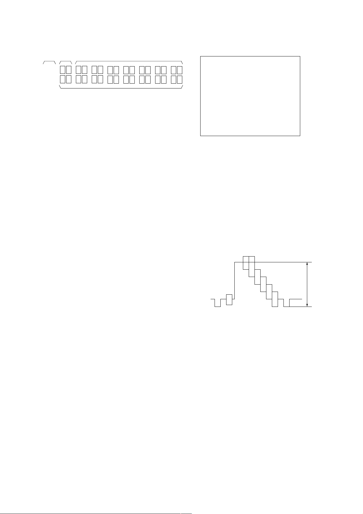
Front Panel
1 2 3 4 5 6 7 8 9 10 11
LOCATION OF PARTS AND CONTROLS
201918171615141312
1 "/1 (POWER) button and indicator
2 DISC tray
3
remote sensor
4 A OPEN/CLOSE button
5 FUNCTION button
6 ./> PREV/NEXT/PRESET +/- button
7 Front Panel Display
Remote
8 H PLAY button
9 X PAUSE button
10 x STOP button
11 VOLUME control
12 DISPLAY button
13 BAND button
14 SOUND FIELD button
15 MUTING button
16 TITLE button
17 DVD MENU button
18 O RETURN button
19 </m/M/, PUSH ENTER button
20 PHONES connector
This section is extracted from
instruction manual.
5

SECTION 3
DISASSEMBLY
Note: Follow the disassembly procedure in the numerical order given.
3-1. LOADING PANEL
3Loading panel
Cam
Hole of chassis
3-2. FRONT PANEL
2Screw (KTP3x8)
2Pull-out the disc tray.
1Turn the cam to the direction of arrow.
3Front panel assembly
1Screw (KTP3x8)
6

3-3. CD MECHANISM
1Screw (BTP3x8)
3Remove the CD mechanism to the direction of arrow.
2Two flat cable
3-4. DISC TRAY
CN002
CN003
Claw
Claw
1Remove the disc tray(Careful of the claw ).
7

SECTION 4
TEST MODE
4-1. GENERAL DESCRIPTION
The T est Mode allows you to make diagnosis and adjustment easily using the remote commander and monitor TV. The instructions,
diagnostic results, etc. are given on the on-screen display (OSD).
4-2. STARTING TEST MODE
Set the FUNCTION to DVD with the main unit power on. Next,
while pushing the [STOP] button and the [MUTING] button on the
main unit at the same time, turn the regulator to the right to start
Test Mode and display the menu shown below on the TV screen.
At the bottom of the menu screen, the model name and revision
number are displayed.
To execute each function, select the desired menu and press its
number on the remote commander. To exit from Test Mode, press
the [POWER] button.
Test Mode Menu
0. Syscon Diagnosis
1. Drive Auto Adjustment
2. Drive Manual Operation
3. Mecha Aging
4. Emergency History
5. Version Information
6. Video Level Adjustment
Exit: Power Key
_
Model : HCX932xxxx
Revision: 1.xxx
4-3. SYSCON DIAGNOSIS
The same contents as board detail check by serial interface can be
checked from the remote commander.
On the T est Mode Menu screen, press
mander, and the following check menu will be displayed.
### Syscon Diagnosis ###
Check Menu
0. Quit
1. All
2. Version
3. Peripheral
4. Servo
5. Supply
6. AV Decoder
7. Video
8. Audio
_
0. Quit
Quit the Syscon Diagnosis and return to the Test Mode Menu.
1. All
All items continuous check
This menu checks all diagnostic items continuously. Normally, all
items are checked successively one after another automatically
unless an error is found, but at a certain item that requires judgment through a visual check to the result, the following screen is
displayed for the key entry.
[0] key on the remote com-
### Syscon Diagnosis ###
Diag All Check
No. 2 Version
2-3. ROM Check Sum
Check Sum = 2005
Press NEXT Key to Continue
Press PREV Key to Repeat
_
For the ROM Check, the check sum calculated by the Syscon is
output, and therefore you must compare it with the specified value
for confirmation.
Following the message, press
or
[PREV] key to repeat the same check again. T o quit the diagno-
sis and return to the Check Menu screen, press
[NEXT] key to go to the next item,
[STOP] or
[ENTER] key. If an error occurred, the diagnosis is suspended
and the error code is displayed as shown below.
### Syscon Diagnosis ###
3-3. EEPROM Check
Error 03: EEPROM Write/Reed N
Address : 00000001
Write Data : 2492
Read Data : 2490
Press NEXT Key to Continue
Press PREV Key to Repeat
_
Press [STOP] key to quit the diagnosis, or [PREV] key to repeat
the same item where an error occurred, or
[NEXT] key to continue
the check from the item next to faulty item.
Selecting 2 and subsequent items calls the submenu screen of each
item.
For example, if “5. Supply” is selected, the following submenu
will be displayed.
### Syscon Diagnosis ###
0. Quit
1. All
2. ARP Register Check
3. ARP to RAM Data Bus
4. ARP to RAM Address Bus
5. ARP RAM Check
_
Check Menu
No. 5 Supply
0. Quit
Quit the submenu and return to the main menu.
1. All
All submenu items continuous check
This menu checks 2 and subsequent items successively. At the
item where visual check is required for judgment or an error occurred, the checking is suspended and the message is output for
key entry. Normally, all items are checked successively one after
another automatically unless an error is found.
8

Selecting 2 and subsequent items executes respective menus and
outputs the results.
For the contents of each submenu, see “Check Items List”.
General Description of Checking Method
2. Version
(2-2) Revision
ROM revision number is displayed.Error: Not detected.
The revision number defined in the source file of ROM (At
the beginning of mass production, the Flash ROM of IC205
is used, but midway it is replaced by the IC206 OTP ROM.
IC205 or IC206) is displayed with four digits.
Below IC205 are all IC205 or IC206.
(2-3) ROM Check Sum
Check sum is calculated.
Error: Not detected.
The 8-bit data are added at addresses 0x000F0000 ~
0x002EFFFF of ROM (IC205) and the result is displayed
with 4-digit hexadecimal number. Error is not detected.
Compare the result with the specified value.
4. Servo
(4-2) Servo DSP Check
Data write → read, and accord check
Error 12: Read data discord
Data 0x9249, 0x2942, 0x4294 are written to the address
0x602 of RAM in the Servo DSP (IC701), then read and
checked.
(4-3) DSP Driver Test
Test signal data → DSP Driver
Error: Not detected.
Caution: Do not conduct this test with a mechanical deck
connected.
The maximum voltage is applied to the Servo Driver IC
(IC801, IC802). If mechanical deck is connected, the motor and optics could be damaged. Disconnect mechanical
deck following the output message, then enter specified 4or 5-digit number from the remote commander, and press
[ENTER]. The test is conducted only when the input
the
data accord. Check the output level, then press the
to finish the test.
This test is skipped if “All” is selected.
[NEXT]
(2-4) Model Type
Model code is displayed.
Error: Not detected.
The model code read from EEPROM (IC201) is displayed
with 2-digit hexadecimal number.
Model Type
DAV-S300 (US) 20
DAV-S300 (E) 22
DAV-S300 (AEP) 23
DAV-S300 (Australian) 24
DAV-S300 (Singapore/Hong Kong) 25
DAV-S300 (Chinese) 26
(2-5) Region
Region code is displayed.
Error: Not detected.
The region code determined from the model code is displayed.
3. Peripheral
(3-2) Gate Array Check
Data write → read, and accord check
Error 02: Gate array write/read discord
Data 0x00~0xFF are written to the address 0xF of GA
(IC601), then read and checked if they accord.
(3-3) EEPROM Check
Data write → read, and accord check
Error 03: EEPROM write/read discord
Data 0x9249, 0x2942, 0x4294 are written to addresses
0x00~0xFF of EEPROM (IC201), then read and checked.
Before writing, the data are saved, then after checking, they
are written to restore the contents of EEPROM.
Supplement: How to disconnect mechanical deck
Disconnect flat cables connected to the CN002 and CN003
of MB-82/85 board. Also, disconnect harness from the
CN011.
5. Supply
Caution: Do not conduct this check with a mechanical deck con-
nected.
An access is made to the stream supply and servo control IC (IC303) and external RAM (IC304) using check
data. If mechanical deck is connected, the motor and
optics could be damaged. This check is also executed by
the “All” menu item.
Supplement: How to disconnect mechanical deck
Disconnect flat cables connected to the CN002 and
CN003 of DVD board. Also, disconnect harness from
the CN011.
(5-2) ARP Register Check
Data write → read, and accord check
Error 08: ARP register write, and read data discord
Data 0x00 to 0xFF are written to the TMAX register (address 0xC6) in ARP (IC303), then they are read and checked.
(5-3) ARP to RAM Data Bus
Data write → read, and accord check
Error 09: ARP ←→ RAM data bus error
Data 0x0001 to 0x8000 where one bit each is set to 1 are
written to the address 0 of RAM (IC304) connected to the
ARP (IC303) through the bus, then they are read and
checked. In case of discord, written bit pattern and read
data are displayed. If data where multiple bits are 1 are
read, the bits concerned may touch each other. Further, if
data where certain bit is always 1 or 0 regardless of written
data, the line could be disconnected or shorted.
9

(5-4) ARP to RAM Address Bus
Data write → other address read discord check
Error 10: ARP → RAM address bus error
Caution: Address and data display in case of an error is
different from the display of other diagnosis (de-
scribed later).
Before starting the test, all addresses of RAM (IC304) are
cleared to 0x0000.
First, 0xA55A is written to the address 0x00000, and the
address data are read and checked from addresses 0x00001
to 0x80000 while shifting 1 bit each. Next, the data at that
address is cleared, and it is written to the address 0x00001,
and read and checked in the same manner. This check is
repeated up to the address 0x80000 while shifting the address data by 1 bit each.
If data other than 0 is read at the addresses except written
address, an error is given because all addresses were already cleared to 0. In this check, the error display pattern is
different from that of other diagnosis; read data, written
address, and read address are displayed in this order. However, the message uses same template, and accordingly exchange Address and Data when reading. The following display, for example,
6. AV Decoder
(6-2) 1930 RAM
Data write → read, and accord check
Error 13: AVD RAM read data discord
The program code data stored in ROM (IC205) are copied
to all areas of RAM (IC402, IC403) connected to the AVD
(IC401) through the bus, then they are read and checked if
they accord. Further, the same test is conducted once again
with the data where all bits are inverted between 1 and 0. If
discord is detected, faulty address, written data, and read
data are displayed following the error code 13, and the test
is suspended.
(6-3) 1930 SP
ROM → A VD RAM → Video OUT
Error: Not detected.
The data including sub picture streams in ROM (IC205)
are transferred to the RAM (IC402, IC403) in AVD (IC401),
and output as video signals from the AVD (IC401).
They are output from all video terminals (Composite, Y/C).
7. Video
### Syscon Diagnosis ###
5-4. ARP to RAM Address Bus
Error 10: ARP - RAM Address B
Address : 0000A55A
Write Data : 00000000
Read Data : 00080000
Press NEXT Key to Continue
Press PREV Key to Repeat
_
shows the data 0xA55A was read from address 0x00080000
though it was written to the address 0x00000000. This implies that these addresses are in the form of shadow. Also,
if the read data is not 0xA55A, another error will be present.
(5-5) ARP RAM Check
Data write → read, and accord check
Error 11: ARP RAM read data discord
The program code data stored in ROM are copied to all
areas of RAM (IC304) connected to the ARP (IC303)
through the bus, then they are read and checked if they accord. If the detail check was selected initially, the data are
written to all areas and read, then the same test is conducted
once again with the data where all bits are inverted between
1 and 0. If discord is detected, faulty address, written data,
and read data are displayed following the error code 11,
and the test is suspended.
(7-2) Color Bar
AVD color bar command write → Video OUT
Error: Not detected.
The command is transferred to the AVD, and the color bar
signals are output from video terminals.
They are output from all video terminals (Composite, Y/C).
8. Audio
(8-2) ARP → 1930
Error 14: ARP → 1930 video NG
15: ARP → 1930 audio NG
10

Check Items List
2) Version
(2-2) Revision
(2-3) ROM Check Sum
(2-4) Model Type
(2-5) Region
3) Peripheral
(3-2) Gate Array Check
(3-3) EEPROM Check
4) Servo
(4-2) Servo DSP Check
(4-3) DSP Driver Test
5) Supply
(5-2) ARP Register Check
(5-3) ARP to RAM Data Bus
(5-4) ARP to RAM Address Bus
(5-5) ARP RAM Check
6) AV Decoder
(6-2) 1930 RAM
(6-3) 1930 SP
7) Video
(7-2) Color Bar
Error Codes List
00: Error not detected
01: RAM write/read data discord
02: Gate array NG
03: EEPROM NG
08: ARP register read data discord
09: ARP ←→ RAM data bus error
10: ARP ←→ RAM address bus error
11: ARP RAM read data discord
12: Servo DSP NG
13: 1930 SDRAM NG
14: ARP → 1930 video NG
15: ARP → 1930 audio NG
16: 1910 UCODE download NG
17: System call error (function not supported)
18: System call error (parameter error)
19: System call error (illegal ID number)
20: System call error (time out)
90: Error occurred
91: User verification NG
92: Diagnosis cancelled
8) Audio
(8-2) ARP → 1930
(8-3) Test Tone
11

4-4. DRIVE AUTO ADJUSTMENT
1. DVD-SL (single layer)
On the T est Mode Menu screen, press [1] key on the remote com-
mander, and the drive auto adjustment menu will be displayed.
## Drive Auto Adjustment ##
Adjustment Menu
0. ALL
1. DVD-SL
2. CD
3. DVD-DL
4. SACD
Exit: RETURN
Normally, [0] is selected to adjust DVD (single layer), CD, DVD
(dual layer), and SACD in this order. But, individual items can be
adjusted for the case where adjustment is suspended due to an
error. In this mode, the adjustment can be made easily through the
operation following the message displayed on the screen.
The disc used for adjustment must be the one specified for adjustment. However, for SACD disc, use the player with initial data if
the disc is not available.
0. ALL
Select [0] and press [ENTER] key, and the servo set data in
EEPROM will be initialized. Then, 1. DVD-SL disc, 2. CD disc,
3. DVD-DL disc, and 4. SACD disc are adjusted in this order.
Each time one disc was adjusted, it is ejected. Replace it with the
specified disc following the message. Though the message to confirm whether discs other than SACD disc are adjusted is not displayed, you can finish the adjustment if pressing the
ton. During adjustment of each disc, the measurement for disc
type judgment is made. As automatic adjustment does not judge
the disc type unlike conventional models, take care not to insert
wrong type discs. Also, do not give a shock during adjustment.
[STOP] but-
Select [1], insert DVD single layer disc, and press [ENTER] key,
and the adjustment will be made through the following steps, then
adjusted values will be written to the EEPROM.
DVD Single Layer Disc Adjustment Steps
1. SLED TIL T Reset
2. Disc Check Memory SL
3. Wait 300 msec
4. Set Disc Type SL
5. LD ON
6. Spdl Start
7. Wait 1 sec
8. Focus Servo ON 0
9. Auto Track Offset Adjust
10. CLVA ON
11. Wait 500 msec
12. Tracking ON
13. Wait 1 sec
14. Sled ON
15. Check CLV Lock
16. Auto LFO Adjust
17. Auto Focus Offset Adjust
18. Auto T ilt Position Adjust
19. Auto Focus Gain Adjust
20. Auto Focus Offset Adjust
21. EQ Boost Adjust
22. Auto LFO Adjust
23. Auto Track Gain Adjust, Search Check
24. 32Tj Fwd
25. 32Tj Rev
26. 500Tj Fwd
27. 500Tj Rev
28. All Servo Stop
29. Eep Copy Loop Filter Offset
12

2. CD
3. DVD-DL (dual layer)
Select [2], insert CD disc, and press [ENTER] key , and the adjustment will be made through the following steps, then adjusted values will be written to the EEPROM.
CD Adjustment Steps
1. Sled Tilt Rest
2. Disc Check Memory CD
3. Wait 500 msec
4. Set Disc Type CD
5. LD ON
6. Spdl Start
7. Wait 500 msec
8. Focus Servo ON 0
9. Auto Track Offset Adjust
10. CLVA ON
11. Wait 500 msec
12. Tracking ON
13. (TC Display Start)
14. Wait 1 sec
15. Jitter Display Start
16. Sled ON
17. Check CLV ON
18. Auto LFO Adjust
19. Auto Focus Offset Adjust
20.
21. Auto Focus Gain Adjust
22. Auto Focus Offset Adjust
23. Eq Boost Adjust
24. Auto LFO Adjust
25. Auto Track Gain Adjust, Search Check
26. 32Tj Fwd
27. 32Tj Rev
28. 500Tj Fwd
29. 500Tj Rev
30. All Servo Stop
Select [3], insert DVD dual layer disc, and press [ENTER] key,
and the adjustment will be made through the following steps, then
adjusted values will be written to the EEPROM.
DVD Dual Layer Disc Adjustment Steps
1. Sled Tilt Reset
2. Disc Check Memory DL
3. Wait 500 msec
4. Set Disc Type DL
5. LD ON
6. Spdl Start
7. Wait 1 sec, Layer 1 Adjust
8. Focus Servo ON 0
9. Auto Track Offset Adjust
10. Clva ON
11. Wait 500 msec
12. Tracking ON
13. Wait 500 msec
14. Sled ON
15. Check CLV Lock
16. Auto Loop Filter Offset Auto Focus Adjust
17.
18. Auto Focus Gain Adjust
19. Auto Focus Offset Adjust
20. Eq Boost Adjust
21. Auto Loop Filter Offset
22. Auto Track Gain Adjust, Search Check
23. 32Tj Fwd
24. 32Tj Rev
25. 500Tj Fwd
26. 500Tj Rev, Layer 0 Adjust
27. Fj (L1 -> L0)
28. Auto Track Offset Adjust L0
29. Clva ON
30. Wait 500 msec
31. Tracking ON
32. Wait 500 msec
33. Sled ON
34. Check CLV Lock
35. Auto Focus Filter Offset
36. Auto Focus Adjust
37.
38. Auto Focus Gain Adjust
39. Auto Focus Offset Adjust
40. Eq Boost Adjust
41. Auto Loop Filter Offset
42. Auto Track Gain Adjust, Search Check
43. 32Tj Fwd
44. 32Tj Rev
45. 500Tj fwd
46. 500Tj Rev, Layer Jump Check
47. Lj (L0 -> L1)
48. Lj (L1 -> L0)
49. All Servo Stop
13

4. SACD
4-5. DRIVE MANUAL OPERATION
Select [4], insert SACD disc, and press [ENTER] key, and the
adjustment will be made through the following steps, then adjusted
values will be written to the EEPROM. However, if SACD disc is
not available, use the player with initial data, skipping the SACD
adjustment. In this case, you can finish the adjustment if pressing
the [STOP] button.
SACD Adjustment Steps
1. Sled Tilt Reset
2. Set Disc Type CD
3. LD ON
4. Spdl Start
5. Wait 500 msec
6. Focus Servo ON 0
7. Auto track Offset Adjust
8.
9. CLVA ON
10. Wait 500 msec
11. Tracking ON
12. Wait 1 sec
13. Sled ON
14. Check CLV ON
15. Auto Focus Offset Adjust
17.
18. Auto Focus Gain Adjust
19. Auto Focus Offset Adjust
20. Eq Boost Adjust
21. Auto LFO Adjust
22. Auto Track Gain Adjust
23. 32Tj Fwd
24. 32Tj Rev
25. 500Tj Fwd
26. 500Tj Rev
On the T est Mode Menu screen, select [2], and the manual operation menu will be displayed. For the manual operation, each servo
on/off control and adjustment can be executed manually.
## Drive Manual Operation ##
1. Disc type
2. Servo Control
3. Track/Layer Jump
4. Manual Adjustment
5. Auto Adjustment
6. Memory Check
0. Disc Check Memory
In using the manual operation menu, take care of the following
points. These commands do not provide protection, thus requiring
correct operation. The sector address or time code field is displayed when a disc is loaded.
1. Set correctly the disc type to be used on the Disc Type
2. After power ON, if the Drive Manual Operation was se-
3. In case of an alarm, immediately press the
Basic operation (controllable from front panel or remote commander)
Operation Menu
Exit: Return
screen.
The disc type must be set after a disc was loaded.
The set disc type is cleared when the tray is opened.
lected, first perform “Reset SLED TILT” by opening 1.
Disc Type screen.
[STOP] but-
ton to stop the servo operation, and turn the power OFF.
27. All Servo Stop */
[POWER] Power OFF
[STOP] Servo stop
[OPEN/CLOSE] Stop+Eject/Loading
[RETURN] Return to Operation Menu or Test Mode
Menu
[NEXT], [PREV] Transition between sub modes of menu
[1] to [9], [0] Selection of menu items
Cursor UP/DOWN Increase/Decrease in manually adjusted
value
14

0. Disc Check Memory
Disc Check
1. SL Disc Check
2. CD Disc Check
3. DL Disc Check
0. Reset SLED TILT
1. Disc Type Auto Check
Disc Type
2. DVD SL 12 cm
3. DVD DL 12 cm
4. CD 12cm
5. SACD 12 cm
6. dvd SL 8 cm
7. DVD DL 8 cm
8. CD 8 cm
9. SACD 8 cm
0. Reset SLED TILT
TC. : : EMG. 00
CD 12 cm
Display when CD 12cm disc was selected
On this screen, the mirror time is measured to judge the disc and it
is written to the EEPROM. First load DVD SL disc and press
next load CD disc and press
and press
[3].
[2], and finally load DVD DL disc
[1],
The adjustment must be executed more than once after default
data were written. External vibration or shock to the player must
not be given. Reference value for DVD is from 10 to 20, and for
CD, from 28 to 4F.
Check that the value of CD is larger than that of DVD.
When those values are beyond a range perform this adjustment
again.
From this screen, you can go to another mode by pressing
[NEXT]
or [PREV] key , but you cannot enter this mode from another mode.
You can enter this mode from the Operation Menu screen only.
1. Disc Type
1. Disc Type Auto Check
2. DVD SL 12 cm
3. DVD DL 12 cm
4. CD 12cm
5. SACD 12 cm
6. dvd SL 8 cm
7. DVD DL 8 cm
8. CD 8 cm
9. SACD 8 cm
0. Reset SLED TILT
Disc Type
EMG. 00
[0] Reset SLED TILT Reset the Sled and Tilt to initial posi-
tion.
[1] Disk Type Check Judge automatically the loaded disc. As
the judged result is displayed at the bottom of screen, make sure that it is correct.
If Disc Check Memory menu has not
been executed after EEPROM default
setting, the disc type cannot be judged.
In this case, return to the initial menu
and make a check for three types of
discs (SL, DL, CD).
[2] to [9] Select the loaded disc. The adjusted
value is written to the address of selected disc. No further entry is necessary if
[1] was selected.
2. Servo Control
1. LD Off R.Sled FWD
2. SP Off L.Sled REV
3. Focus Off
4. TRK. Off
5. Sled Off
6. CLVA Off
7. FCS. Srch Off
Servo Control
On this screen, select the disc type. To select the disc type, press
the number of the loaded disc. The selected disc type is displayed
at the bottom. Selecting
[1] automatically selects and displays the
disc type. In case of wrong display, retry “Disc Check Memory”.
Also, opening the tray causes the set disc type to be cleared. In
this case, set the disc type again after loading.
In performing manual operation, the disc type must be set.
Once the disc type has been selected, the sector address or time
code display field will appear as shown below. These values are
displayed when PLL is locked.
1. Disc Type Auto Check
2. DVD SL 12 cm
3. DVD DL 12 cm
4. CD 12cm
5. SACD 12 cm
6. dvd SL 8 cm
7. DVD DL 8 cm
8. CD 8 cm
9. SACD 8 cm
0. Reset SLED TILT
DVD SL 12 cm
Disc Type
SA. SI. EMG. 00
Display when DVD SL 12cm disc was selected
0. Reset SLED TILT
SA. SI. EMG. 00
DVD SL 12 cm
On this screen, the servo on/off control necessary for replay is
executed. Normally, turn on each servo from 1 sequentially and
when CL VA is turned on, the usual trace mode becomes active. In
the trace mode, DVD sector address or CD time code is displayed.
This is not displayed where the spindle is not locked.
The spindle could run overriding the control if the spindle system
is faulty or RF is not present. In such a case, do not operate CL VA.
15

[0] Reset SLED TILT Reset the Sled and Tilt to initial posi-
tion.
[1] LD Turn ON/OFF the laser.
[2] SP Turn ON/OFF the spindle.
4-6. MECHA AGING
### Mecha Aging ###
[3] Focus Search the focus and turn on the focus.
[4] TRK Turn ON/OFF the tracking servo.
[5] Sled Turn ON/OFF the sled servo.
[6] CLVA Turn ON/OFF normal servo of spindle
servo.
[7] FCS. Srch Apply same voltage as that of focus
search to the focus drive to check the
focus drive system.
→ Sled FWD Move the sled outward. Perform this
operation with the tracking servo turned
off.
← Sled REV Move the sled inward. Perform this op-
eration with the tracking servo turned
off.
↑ Tilt UP Move the tilt upward.
↓ Tilt DOWN Move the tilt downward.
The following menus are normally not used.
3. Track/Layer Jump
4. Manual Adjustment
5. Auto Adjustment
The persons who do not know well about these menus should not
use them.
1. TRAY Aging
2. SEARCH Aging
Abort: STOP key
On the Test Mode Menu Screen, selecting [3] executes the aging
of the mechanism. TRA Y aging or SEARCH aging are selected by
[1] or [2]. Start aging with PLA Y. During aging, the repeat cycle is
displayed. Aging can be aborted at any time by pressing the [STOP]
key. After the operation is stopped, press the [STOP] key or [RE-
TURN] key again to return to the Test Mode Menu. SEARCH Aging is only for a CD.
4-7. EMERGENCY HISTORY
### MEG. History ###
Laser Hours CD xxxxxxxh
DVD xxxxxxxh
1. 00 00 00 00 00 00 00 00
00 00 00 00 00 00 00 00
2. 00 00 00 00 00 00 00 00
00 00 00 00 00 00 00 00
Select: 1 – 9 Scroll: UP/DOWN
(1: Last EMG.) Exit: Return
On the Test Mode Menu screen, selecting [4] displays the information such as servo emergency history. The history information
from last 1 up to 10 can be scrolled with ↑key or↓key. Also,
specific information can be displayed by directly entering that
number with ten keys.
6. Memory Check
EEPROM DATA
CD – DVD –
ID No. 00 SACD SL L0 L1
Focus Gain xx xx xx xx xx
TRK. Gain xx xx xx xx xx
Focus Offset xx xx xx xx xx
TRK. Offset xx xx xx xx xx
L. F. Offset xx xx xx xx xx
EQ Boost xx xx xx xx xx
Jitter xx xx xx xx xx
Mirror Time xx xx xx xx xx
_
CLEAR: Default Set
This screen displays current servo adjusted data stored in the
EEPROM. Though adjusted data can be initialized with the
[CLEAR] key, they cannot be restored after initialization.
So, before clearing, make a note of the adjusted data.
For reference, the drive has been designed so that the gain center
value is 20 and offset value is 80. Other values will be in a range
of 10 to 80. If extreme value such as 00 or FF is set, adjustment
will be faulty. In such a case, check for disc scratch or cable disconnection, then perform adjustment again.
16
The upper two lines display the laser ON total hours. Data below
minutes are omitted.
Clearing History Information
Clearing laser hours
[DISPLAY] and [CLEAR] keys in this order.
Press
Both CD and DVD data are cleared.
Clearing emergency history
[TITLE] and [CLEAR] keys in this order.
Press
Initializing set up data
Press
[DVD] and [CLEAR] keys in this order.
The data have been initialized when “Set Up Initialized” message is displayed. The EMG. History screen will be restored
soon.
How to see Emergency History
31.12
4-8. VERSION INFORMATION
## Version Information ##
2
1 : Emergency Code
2 : Don’t Care
These codes are used for verification of software designing.
3 : Historical order 1 to 9
Emergency Codes List
10: Communication to IC001 (TK board) failed.
11: Each servo for focus, tracking, and spindle is unlocked.
12: Communication to EEPROM, IC201 (DVD board) failed.
13: Writing of hours meter data to EEPROM, IC201 (DVD board)
failed.
14: Communication to Servo DSP IC701 (DVD board) failed, or
Servo DSP is faulty.
20: Initialization of tilt servo and sled servo failed. They are not
placed in the initial position.
21: Tilt servo operation error
22: Syscon made a request to move the tilt servo to wrong posi-
tion.
23: Sled servo operation error
24: Syscon made a request to move the sled servo to wrong posi-
tion.
30: Tracking balance adjustment error
31: Tracking gain adjustment error
32: Focus balance adjustment error
33: Focus bias adjustment error
34: Focus gain adjustment error
35: Tilt servo adjustment error
36: RF equalizer adjustment error
37: RF group delay adjustment error
38: Jitter value after adaptive servo operation is too large.
40: Focus servo does not operate.
41: With a dual layer (DL) disc, focus jump failed.50: CLV
(spindle) servo does not operate.
51: Spindle does not stop.
60: With a DVD disc, Syscon made a request to seek nonexistent
address.
61: With a CD disc, Syscon made a request to seek nonexistent
address.
62: With a CD disc, Syscon made a request to seek nonexistent
track No. and index No.
63: With a DVD disc, seeking of target address failed.
64: With a CD disc, seeking of target address failed.
65: With a CD disc, seeking of target index failed.
70: With a DVD disc, physical information data could not be read.
71: With a CD disc, TOC data could not be read.
80: Disc type judgment failed.
81: As disc type judgment failed, retry was repeated.
82: As disc type judgment failed, a measurement error occurred.
83: Disc type could not be judged within the specified time.
84: Illegal command code was received from Syscon.
85: Illegal command was received from Syscon.
IF con. Ver. x. xxx (xxxx)
Group 00
SYScon. Ver. x. xxx (xxxx)
Model xx
Region 0x
SW1 ??
SW2 ??
Exit: RETURN
On the Test Mode Menu screen, selecting [5] displays the ROM
version and region code.
The parenthesized hexadecimal number in version field is
checksum value of ROM.
4-9. VIDEO LEVEL ADJUSTMENT
On the Test Mode Menu screen, selecting [6] displays color bars
for video level adjustment. During display of color bars, OSD disappears but the menu screen will be restored if pressing any key.
Measurement point : LINE OUT VIDEO
(75 Ω terminating resistance)
Measuring instrument:Oscilloscope
Adjustment device :RV401 on DVD board
Specified value : 1.0 ± 0.02 Vpp
1.0 ± 0.02 Vp-p
17
SECTION 5
ELECTRICAL ADJUSTMENTS
In making adjustment, refer to 5-2. Adjustment
Related Parts Arrangement.
Note: During diagnostic check, the characters and color bars can
be seen only with the NTSC monitor. Therefore, for diagnostic check, use the monitor that supports both NTSC and
PAL modes
This section describes procedures and instructions necessary for
adjusting electrical circuits in this set.
Instruments required:
1) Color monitor TV
2) Oscilloscope 1 or 2 phenomena, band width over 100 MHz,
with delay mode
3) Frequency counter (over 8 digits)
4) Digital voltmeter
5) Standard commander
* RM-SS300 (1-418-838-11)
6) DVD reference disc
HLX-501 (J-6090-071-A) (dual layer)
HLX-503 (J-6090-069-A) (single layer)
HLX-504 (J-6090-088-A) (single layer)
HLX-505 (J-6090-089-A) (dual layer)
7) SACD reference disc
HLXA-509 (J-6090-090-A)
5-1. ADJUSTMENT OF VIDEO SYSTEM
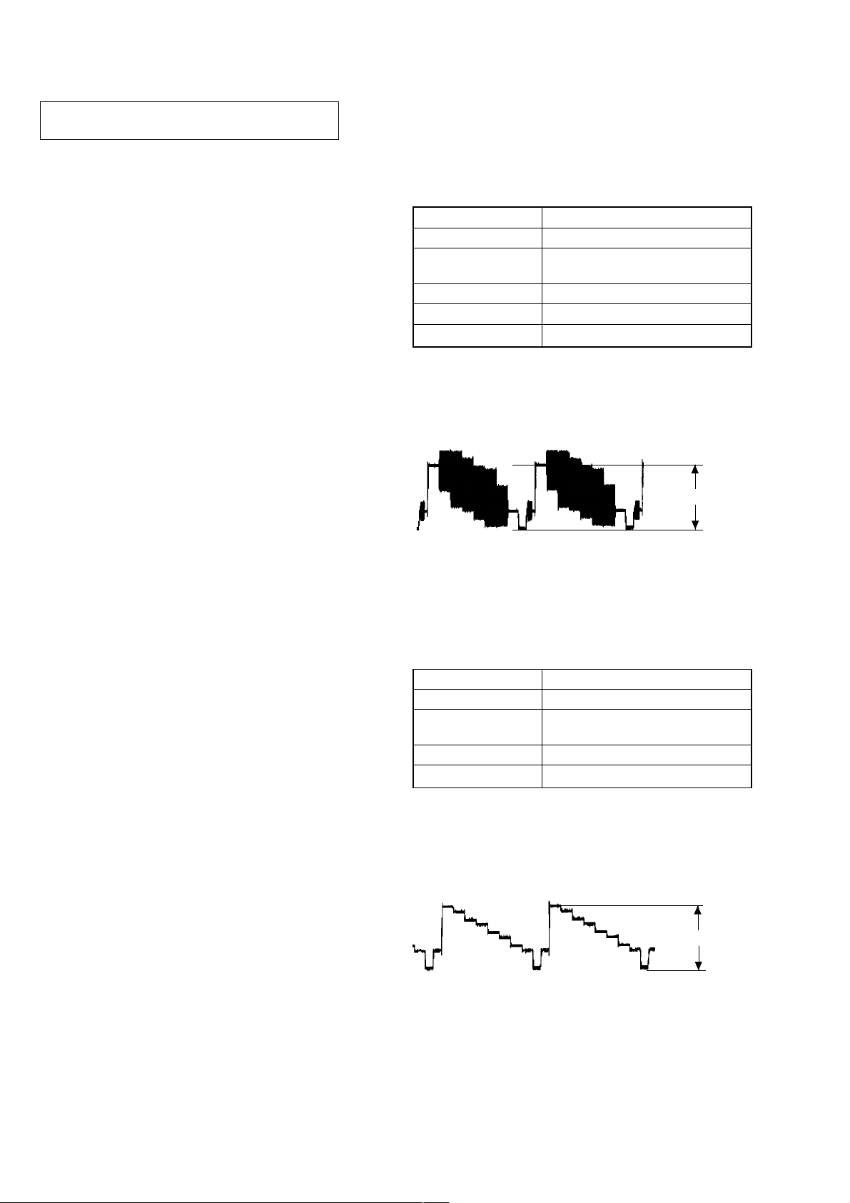
1. Video Level Adjustment (DVD BOARD)
<Purpose>
This adjustment is made to satisfy the NTSC standard, and if not
adjusted correctly, the brightness will be too large or small.
Mode Video level adjustment in test mode
Signal Color bars
Test point
Instrument Oscilloscope
Adjusting element RV401
Specification 1.0 ± 0.02 Vp-p
Adjusting method:
1) In the test mode initial menu “6” Video Level Adjustment, set
so that color bars are generated.
2) Adjust the RV401 to attain 1.0 ± 0.02 Vp-p.
LINE OUT (VIDEO) connector
(75 Ω terminated)
1.0 ± 0.02 Vp-p
* Use only the designated remote control when adjusting this
system component.
Figure 5-1
2. S-terminal Output Check (DVD BOARD)
<Purpose>
Check S-terminal video output. If it is incorrect, pictures will not
be displayed correctly in spite of connection to the TV with a Sterminal cable.
Mode Video level adjustment in test mode
Signal Color bars
Test point
Instrument Oscilloscope
Specification 1.0 ± 0.1 Vp-p
Checking method:
1) In the test mode initial menu “6” Video Level Adjustment, set
so that color bars are generated.
2) Confirm that the S-Y level is 1.0 ± 0.1 Vp-p.
S VIDEO OUT (S-Y) connector
(75 Ω terminated)
1.0 ± 0.1 Vp-p
18
Figure 5-2

VIDEO board
TUNER board
AUDIO board
DIAGRAMS
SECTION 6
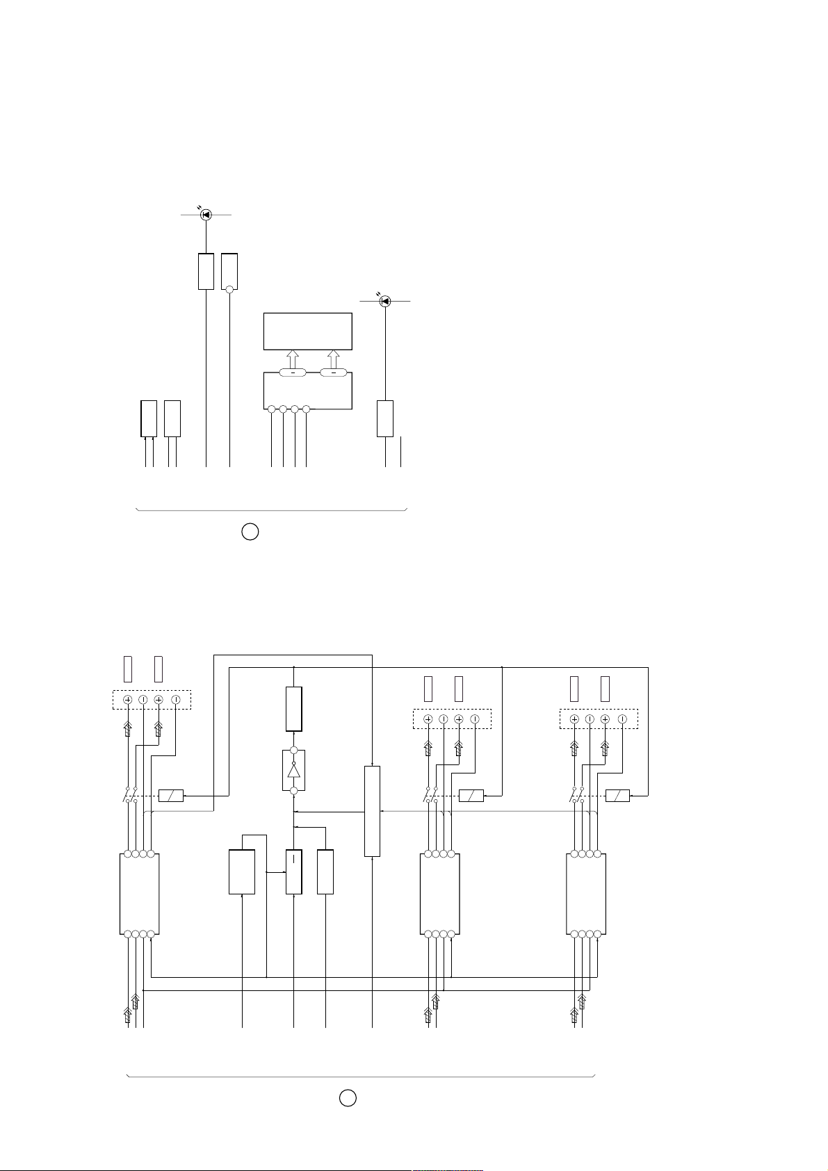
6-1.CIRCUIT BOARDS LOCATION
POWER board
PROTECT board
TK board
LOADING board
PW-932 board
DVD board
LV-932 board
HP-932 board
SW-932 board
FP-932 board
19 19
ARRANGEMENT
5-2. ADJUSTMENT RELATED PARTS
DVD BOARD (SIDE A)
3. Checking S Video Output S-C (DVD BOARD)
<Purpose>
Mode Video level adjustment in test mode
This checks whether the S-C satisfies the NTSC Standard. If it is
not correct, the colors will be too dark or light.
76
CN005
Signal Color bars
Test point CN005 pin 6
12
Instrument Oscilloscope
Specification 286 ± 50 mVp-p
CN005
100µF
Connection:
Oscilloscope
6
+
100k
75Ω
±1%
±1%
RV401
VIDEO LEVEL ADJ
286 ± 50 mVp-p
5
Figure 5-3
Checking method:
1) Confirm that the S-C burst is 286 ± 50 mVp-p.

1.2Vp-p
1Vp-p
0.75Vp-p
2.4Vp-p
2Vp-p
0.75Vp-p
H
IC700 5
1
– VIDEO SECTION –
536
mVp-p
IC001 1 DVD PLAY
200mV/DIV 100ns/DIV
1
– TK SECTION –
1.0Vp-p
H
IC401 ya
9
– DVD (4/12) SECTION –
2
880
2
0.75Vp-p
q;
H
IC702 9
3
mVp-p
IC001 1 CD PLAY
500mV/DIV 500ns/DIV
3
IC401 ys
H
qa
IC702 1
H
592mVp-p
IC001 wl DVD PLAY
200mV/DIV 500ms/DIV
1.2Vp-p
IC401 yg
H
H
IC701 qd, qg
5
4
448mVp-p
4
qs
– DVD (5/12) SECTION –
6
IC001 wl CD PLAY
200mV/DIV 20ms/DIV
5
1.5Vp-p
IC303 qj DVD PLAY
500mV/DIV 100ns/DIV
H
IC701 qa
1.3Vp-p
IC001 el DVD PLAY
500mV/DIV 50ms/DIV
1.5Vp-p
500mV/DIV 500ns/DIV
qd
H
7
1.7Vp-p
500mV/DIV 200ms/DIV
6
IC303 ql CD PLAY
qf
– DVD (8/12) SECTION –
Q700 E
180mVp-p
IC001 el CD PLAY
100mV/DIV 50ms/DIV
7
2.1Vp-p
IC202 os
12.4MHz
860mVp-p
IC001 r; DVD PLAY
500mV/DIV 50ms/DIV
8
2.5Vp-p
IC202 5
24.9MHz
qg
1.5Vp-p
IC001 r; CD PLAY
500mV/DIV 100ns/DIV
9
1.8Vp-p
16MHz
qh
– DVD (10/12) SECTION –
1.5Vp-p
IC001 tf DVD PLAY
IC001 tf CD PLAY
500mV/DIV 500ns/DIV
q;
IC903 qg
3.4Vp-p
1
WAVEFORMS
– DVD (1/12) SECTION –
2.1Vp-p
IC001 6
27.0MHz
2
W or less unless otherwise
4
/
1
IC001 qs
33.8MHz
2.8Vp-p
2Vp-p (DVD)
2.4Vp-p (CD)
IC001 qd
24.5MHz
3
4
IC001 qj
DVD : 36.8MHz
CD : 33.8MHz
– DVD (2/12) SECTION –
1.4Vp-p
500mV/DIV 50ms/DIV
5
1.7Vp-p
IC701 yl DVD PLAY
500mV/DIV 200ms/DIV
6
220mVp-p
IC701 yl CD PLAY
100mV/DIV 50ms/DIV
7
440mVp-p
IC701 yk DVD PLAY
8
IC701 yk CD PLAY
500mV/DIV 50ms/DIV
These are omitted
EB
C
Q
20 20
HCD-S300
50 WV or less are not indicated except for electrolytics
THIS NOTE IS COMMON FOR PRINTED WIRING
BOARDS AND SCHEMATIC DIAGRAMS.
(In addition to this, the necessary note is printed
in each block.)
and tantalums.
For schematic diagrams.
Note:
• All capacitors are in µF unless otherwise noted. pF: µµF
: internal component.
f
specified.
•
• 2 : nonflammable resistor.
• 5 : fusible resistor.
• All resistors are in Ω and
fied by mark 0 or dotted
line with mark 0 are criti-
cal for safety.
Note:
The components identi-
• C : panel designation.
number specified.
Replace only with part
under no-signal (detuned) conditions.
• U : B+ Line.
• V : B– Line.
• H : adjustment for repair.
• Voltages and waveforms are dc with respect to ground
service mode.
Voltage variations may be noted due to normal produc-
tion tolerances.
no mark : STOP
J : DVD/CD
c : AUDIO
g : VIDEO
L : C
K : Y
SP : Singapore model.
HK : Hong Kong model.
AUS : Australian model.
MX : Mexican model.
CND : Canadian model.
• Voltages and waveforms are dc with respect to ground in
• Waveforms are taken with a oscilloscope.
• Circled numbers refer to waveforms.
• Signal path.
• Abbreviation
E32 : Cantral & South America model.
: Through hole.
a
• b : Pattern from the side which enables seeing.
For printed wiring boards.
(The other layers' patterns are not indicated.)
Note:
• X : parts extracted from the component side.
•
• Indication of transistor
These are omitted
EB
C

HCD-S300
DVD RF
IC701
SERVO DSP
A
(Page 23)
SIGNAL PROCESS/
VIDEO SECTION
CD RF
MDP0
LOCK
MDS0
22
FG REF
ADC068ADC167ADC266ADC365ADC4
69
+3.3V
IC702 (2/2)
TRREF
TRIN23FGIN
20
21
7 5
7481849396
VRBA,
DAB 0-3
41ı44
GIO 5-8
GIO 11
38
DFCTI
28
FCSON
XSDPIT
XSDPRD
XSDPWR
1
2
39
128
HRD
HINT
HWR
GIO 10
DAB 0, 1
DAB 2,3
8085929748
TRD
FCD
FCD
2
3
XSDPCS
3
HCS
Q801
9
HA0, 1
4
5
EA 0, 1
GIO 1, 2
49
TLTA,TLTB
(1/2)
D805
TRD
5
7ı9
SLDA, SLDB,
IC702 (1/2)
6
117ı120
PWM 0-2
STVC
3 1
7
HD8-15
122
HD 0-7
TILT MUTE
125
GIO 4
46
20
X2/CLKIN
RS
GIO 0
50
FGMODE
D805 (2/2)
TLTA, TLTB
23
26 108
26
B
MAIN SECTION
N27MSDP
XSDPRST
14
IC803 (1/2)
12
(Page 22)
D701
13
X3VRST
D801
(1/2)
D807
GAIN
CONTROL
Q802, 803
26
SPDLSTOP
D802
D801 (2/2)
20
SPGAIN
XDRV MUTE
SLDA, SLDB,
STVC
235
LDMM/DMM
LDMP/DMP
OCSW1
OCSW2
CKSW1
2.5VC
2VC
1.6VC
8
IC803 (2/2)
+5V
+3.3V
D803 (2/2)
D803 (1/2)
9
6
24
3 1
5 7
10
21 21
IC001
DVD/CD RF AMP
DIGITAL SERVO
RF
OPTICAL DEVICE
SIGO
RF IP
1 54
40TE39PI29
FE
9
A-D
ı
A-D
12
PDIC
DVD/CD
5ı8
A2-D2
26
MIRR
E-H
13ı16
E-H
COIL
COIL
DRIVE
FOCUS
IC801
FOCUS/TRACKING COIL
TILT MOTOR DRIVE
13
14
2VC
Q002
32
33
VCI
TZC
VC
17
VC
SCLK
43ı46
SWD
PD
27
42
31
DFT
SRD
SDEN
FDCHG
HOLD2
PD
LD
19
20
Q001
LD DRIVE
LD
DVD/CD
LD MODULE
VR
FCSFOCUS
COIL
DRIVE
TRACKING
11
12
TRK
COIL
TRACKING
TILT
15ı18
TIA, TIB
TILT
MOTOR
M
MOTOR
DRIVE
INLIM
INLIMIT
SENSOR
MOTOR
SPINDLE
15
16
SPM
M
MOTOR
SPINDLE
DRIVE
SLED
MOTOR
11ı14
SLA, SLB
M
SLED
DRIVE
MOTOR
MOTOR
LOADING
17
18
M
M001
LOADING
DRIVE
IC802
SLED MOTOR, SPINDLE MOTOR
LOADING MOTOR DRIVE
OCSW 1, 2
S001
TRAY SENSOR
MOTOR
CKSW1
S002
CHUCK SENSOR
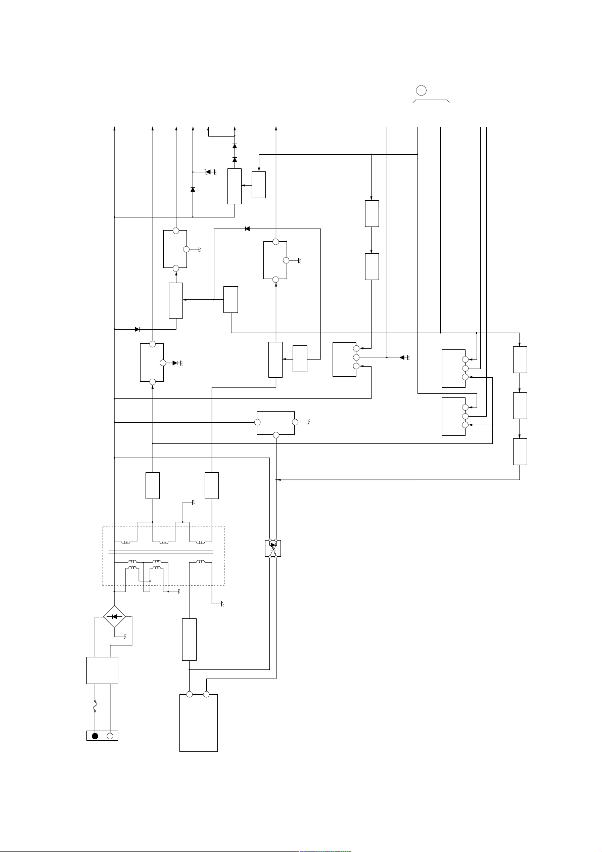
– RF/SERVO SECTION –
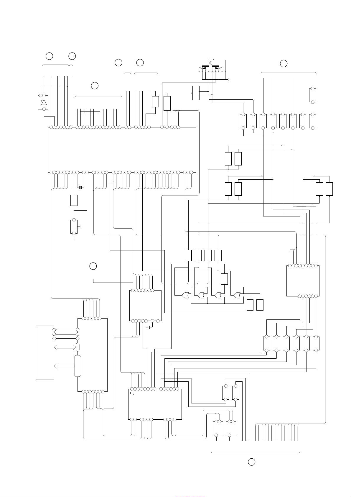
6-2. BLOCK DIAGRAMS
09

IC203
(
g
)
BUFFER
E
XVIFCS
IFSC0
11
4Y2Y1Y
4A2A1A
12
CS0L
SC0
AUDIO MAIN
SECTION
IFSO0
4 6
1 3
SO0
(Page 24)
IFSI0
SI0
XFRRST
XFRRST
XIFINT
FCSON
XSDPRST
XSDPIT
XSDPWR
XSDPRD
B
XSDPCS
RF/SERVO SECTION
(Page 21)
LDMP/DMP
LDMM/DMM
SPGAIN
XDRVMUTE
OCSW1
SPDLSTOP
OCSW2
CKSW1
IC206
IC205
IC204
16M FLASH
16M FLASH
1M SRAM
HD 0-15
HA 1-20
WE, CE
OE
OE, CE
WE, RY/BY,
HD 0-15
HA 1-20
OE, UB, LB
CS, WE,
HD 0-15
HA 1-16
S550D/S705D
HD 8-15
+3.3V
IC207
CS0L
XFRRST
SC0
SO0
SIO
HD 0-15
HA 0-21
126-133146-154
HA 0-5, 17-19
IC201
4K EEPROM
RESET
POWER ON
4 5
HD 0-7
XECS24XEWC
23
CS
4 3
SC0
76 77 78 14 97
25-39 41
42 44-64
HA 0-5, 17-19
WC
DIDOSK
5 8
SI0
SO0
CE
RST
SC0
SO0
SI0
XEBSY
25
R/B
6 1
11
CS0
CS0L
WE
D 16-31
A 01-15
CS
HGA
IC601
4
112
113
RY/BY, OE
WE, UB, LB,
22
XIFINT
CS1
124
125
141
10722
CS1
IC202
SYSTEM CONTROL
54
114
FCSON
SDPRST
CS4
HRD
HWRH
HWRL
142
145
144
143
23
241994
RD
CS4
WR0
WR1
115
SDPIT
WAIT
157
RDY
116
SDPWR
XINT1
156
INT1
117
SDPRD
XINT3
155
88
INT3
57
94939291646388
118
SDPCS
SPGAIN
SPDLSTOP
XDRVMUTE
CPUCK
RST
3
135
5
83
CLK
PF7/OCPA0/ATG
LDMP/DMP
LDMM/DMM
MUTE
MD2
98
99
MD2
MUTE
XRD
XWRH
X1
91
CKSW1
OCSW1
OCSW2
NORF
DFCT
FWON
LOCK
102
103
104
105
DFCT
LOCK
NORF
FWON
C
SIGNAL PROCESS/
VIDEO SECTION
(Page 23)
DACK1
XCS2
XCS3
XAVDIT
9
8
958485
CS2
CS3
INT0
DACK1
X0
92
ARPRST
106
107
XARPRST
DACK0
DREQ1
86
DACK0
DREQ1
ARPINT
XARPIT
C
108
XARPWT
DREQ0
87
DREQ0
ARPWR
ARPRD
ARPCS
AVDWT
ARPWT
727127VS53
109
110
111
XARPCS
XARPRD
XAVDWT
XARPWR
(Page 23)
VIDEO SECTION
SIGNAL PROCESS/
XIF0K
96
RAS0/PB0
RAS1/PB4
A22/P66
66 100
AVDRST
57RST
X57RST
XAVDRST
DVD/CD
CKSEL
MCK
59
VS
N27MHGA
e 21
Pa
RF/SERVO SECTION
B
22 22
N27MSDP
IC001
PLL
27MARP
SCKO3
MDMLXT1
1
19
256FS30
121714
SCKO2
6
C
33MARP
SCKO1
33M30
SIGNAL PROCESS/
VIDEO SECTION
(Page 23)
27M30
527
IC004
361
HCD-S300
– MAIN SECTION –
HA 0-21
HD 0-15
C
(Page 23)
VIDEO SECTION
SIGNAL PROCESS/
HA 0, 1
B
HD 8-15
(Page 21)
SECTION
RF/SERVO
X3VRST
X201
12.5MHz
X001
27MHz
09

HCD-S300
J
SPDIF
AUDIO MAIN
SECTION
(Page 24)
VIDEO V
D
VIDEO Y
I/O, TUNER
SECTION
(Page 25)
VIDEO C
V S
IC304
16M DRAM
IC402, 403
16M SDRAM
XRAS, XOE
HD 00-15
MA 0-9
XRAS, XOE
XMWR, XCAS,
CLK, CKE,
DDT 0-15
DAD 0-11
XMWR, XCAS,
CS, WE, CAS, RAS
DQML, DQMU,
125 127
120-123
129-132
134 135
137 138
140 141
105-108
110-113
115-118
148
150-152
154-157
159-162
164-167
146 147
136-139
141-144
27
143 144
146 147
149 150
38ı434546
SD 0-7
97
98
169-172
RFIN1
RFIN2
17
19
152 153
DT 0-7 I
100ı105
SD 0-7
155 156
MDS0
49
52
MDP0
SDCK, SDEF,
91
IC303
47ı51
XSHD, XSAK, XSRQ
93ı96
65
COMP OUT
ARP2
61
Y OUT
29ı32
CDDOUT, CDDATA,
CDBCK, CDLRCK
107ı110
DFCT
NORF
LOCK
555658
62
C OUT
FWON
59
MD2
113
MUTE
111
ADJ
VIDEO
LEVEL
RV401
VREFI
70
HD 0-15
HAD 0-21 I
168-170 172-178 180-187 189-192 2-5 7-10 12-15 205-208
+5V
SCLKIN
CLKI
160 163
CRPCLKIN
ACLKIN
RSTIN
103 19 36
166
167
193
194
196
198ı202
D 0-7
63-68 70 71
A 0-7
73-76 79-82
SCKI
123
MCKI
121
XRST
XWR
60
XRD
61
XINT
XCS
838486
XWAT
87
27MARP
27M30
33M30
256FS30
XAVDRST
33MARP
XARPRST
CDDOUT, CDDATA, CDBCK, CDLRCK
HD 0-15
HA 0-21
23 23
HD 8-15
HA 0-7
IC305
8M DRAM
HD 00-15
MA 0-9
– SIGNAL PROCESS/VIDEO SECTION –
DVD RF
A
CD RF
RF/SERVO
MDS0
MDP0
(Page 21)
SECTION
LOCK
DFCT
NORF
LOCK
FWON
MD2
MUTE
XARPWR
XARPRD
XARPIT
XARPCS
XARPWT
XCS2
XCS3
HD 0-15
XRD
XWRH
XAVDIT
XAVDWT
DACK0
DREQ0
DACK1
DREQ1
XARPRST
XAVDRST
33MARP
256FS30
33M30
27M30
27MSRP
MAIN
C
(Page 22)
SECTION
HA 0-21
VS
09
IFSIO
E
IFSO0
SECTION
(Page 22)
AUDIO MAIN
IFSCO
XFRRST
XIFINT
XVIFCS
C
XIFOK
(Page 23)
VIDEO SECTION
SIGNAL PROCESS/
I
POWER SECTION
(Page 27)
H
SECTION
(Page 26)
AMP SERVO
J300
PHONES
H
SECTION
(Page 26)
AMP SERVO
R
SL
L
SR
SW
C
IC908
BUFFER
IC901
1
2 6
SO0
SIO
1
100
IFSIO
IFSDO
IC903
AUDIO SYSTEM CPU
YSSCSB
YSSCS
43567
42315
YCSB
CS
20
OE
22
WE
27
STATIC RAM 256KB
G
(Page 26)
DISPLAY SECTION
EN-A/PA3
EN-B/PA4
KEY1
KEY2
DIM1/PA1
DIM2/PA2
FLDATA
FLINH
SCO
XFRRST
IFBSY
XIFCS
XIFOK
ENA
ENB
KEY1
KEY2
DIM1
DIM2
PA3
PA4
FLDATA
FLINH
FLCLK
262735283738363942
P3
P4
FLINH
D2/P2
FLDATA
CDT1PDSMUTE
7071696867
282930
32
SMUTE
J
(Page 23)
VIDEO SECTION
SIGNAL PROCESS/
SPDIF
5
65
62
IC
NO USE
AUDIO DIGITAL PROCESSOR
SDIA0
83
84
BCK
SAU3
LRCK
D.DATA
IFSCO
YSSSI
77
XFRRST
YSSSO
76274
XIFINT
YSSSCK
XVIFCS
YSSIC
10
D0-D7
A0-A14
73
ENA
IFOK
AN/DIG
RESET
XOUT
11
121315
Q901
RESET
IC902
RESET
1 3
+5.6V
2
89
88
72-79
25-29,42-44,58-59
9495922593
ENB
KEY1
KEY2
XIN
STOPCSCLK
18
X901
16MHz
1234YCSB
68
69SO67CS66
SI
SCK
CS
OE
WE
61,64,70,86-87
SDIA1
NO USE
47
85
SAU1
SAU2
A.DATA
D1/P1
IC904
NO USE46NO USE45SDWCK082SDDCK0
FLCLK
FLCLK
FLCE
114
FLCE
SLED
FLCS
DIRERR
113
DVD-POWER
STBY-LED
SIRCS
SIR
DVDPW
78
STBY
SIRCS
DVDPOW
DIRDO
DIRDI
DIRCDE
DIRCLK
8687858483
112
111
110
IC907
AUDIO DIGITAL PROCESSOR
IC906
AUDIO A/D CONV
POWER
PW
44
POWRY
MODEL1
82
109
BCK
32
BCK
DVD-POWER
SLEEP
RLY
45
SWMODE/SLEEP
ASEL1
AS1
AS2
109
110
5
48
DIN2
XMODE
BCK
LRCK
15
14
LRCK
D.DATA
SMUTE
30
3
17
43
PD
S/M
CDT1
BCLK
LRCK
5
4
LRCK
FAULT/BTCE1
RLY
AMP-MUTE
Q902
AMP-MUTE
FAULT
43
556354
F-RLY
AMP-MUTE
FAULT/BTCE1
PROTECT/BTCE2
ASEL2
AU-MUTE
V-MUTE
VSEL1
VSEL2
201921
22
232448477572535251
VS1
VS2
VMUTE
TUNCLK
111
112
113
114
37DI36
38
35
34
CE
DO
CLK
ERROR
DATAO16CKOUT13XOUT
12.288MHz XIN22DIN0
21
MCK
X503
12.288MHz
29
28
MCK
42CS41
39
38
XTI
CCLK
MCLKI
SDTI16SDTI27SDTI2
SDTO
8
9
SAU2
SAU3
SAU1
A.DATA
PROTECT/BTCE2
SWITCH
HP-SW
66
HP-SW
TUNCLK
TUNCE
RDS2
RDS2
RDS1
TUNCE
3
D.IN
LRW
24
23
33
VREFL
LOUT3
ROUT3
RIN+32RIN-31LIN+30LIN-
Q909
65
HP-MUTE
RDS1
TUNND
C
25
LOUT2
MUTE SW
LR-MUTE
TUNNED
TUN-DO
TUNDO
ROUT226ROUT1
TUNDI
SR
28
29
605961
SWMUTE
CS-MUTE
TUNDIN
TUNMUTE
50
TUNSTM
SL
27
LOUT1
D911
VOL-CE
VCE
VOL-DAT
575658
VCLK
VDATA
Q906
SWITCH
LR-MUTE
Q300-Q301
VOL-CLK
MUTE
Q907
SWITCH
SW MUTE
D912
Q908
SWITCH
CS-MUTE
D913
AUMUTE
Q910
7
IC503
6
RIN
SWITCH
1
BUFFER
Q503
Q505
Q905
MUTE
L
IC509(1/2)
5 7
MUTE SW
MUTE SW
BUFFER
7
IC502
6
LIN
D914
1
BUFFER
Q504
Q506
R
BUFFER
IC509(2/2)
3 7
IC508(1/2)
5 7
MUTE SW
MUTE SW
R
BUFFER
L
Q903
D.IN
BUFFER
IC508(2/2)
3 1
MUTE
AS1
ASEK1
IC510
LPF AMP
3 7
L
R
SL
BUFFER
BUFFER
IC513(1/2)
IC513(2/2)
L
BUFFER
IC504(1/2)
5 7
VS1
VM
VSEL1
IC512(1/2)
3 1
5 7
IC507
R
BUFFER
IC504(2/2)
3 1
VS2
RDS2
RDS1
TUNCE
TUNCLK
CE
CK
RDS2
VSEL2
5 7
Q904
MUTE
AS2
VMUTE
AUMUTE
ASEL2
AUMUTE
SR
BUFFER
BUFFER
IC512(2/2)
3 1
VDATA
VCLK
VCE
15
16
STB
DATA
AUDIO MAIN VOL
C
SW
BUFFER
IC505(1/2)
IC505(2/2)
5 7
TUNDI
TUNND
TUNDO
DI
DO
TUNED
SW/RDS1
14
CK
LOUTA3LOUTB6LOUTC
L-INA
4
BUFFER
3 1
TUNSTM
TUNSTM
C
BUFFER
IC511(1/2)
5 7
9
LINB
LINC
7
10
SL
IC506(1/2)
5 7
SW
IC511(2/2)
3 1
ROUTA26ROUTB23ROUTC
RINA25RINB
22
BUFFER
BUFFER
20
RINC
19
SR
BUFFER
IC506(2/2)
3 1
Q501
MUTE SW
Q502
MUTE SW
24 24
HCD-S300
– AUDIO MAIN SECTION –
F
SECTION
I/O,TUNER
(Page 25)
09
HCD-S300
IC701
BUFFER
VIDEO(MONITOR OUT)
J700(2/3)
151
3
VIDEO OUT(VIDEO1)
134
12
+5V
J700(3/3)
DVD OUTPUT
1
3
4
2
11
BUFFER
Q700,703-704
7
10
3
Q701-702
DC OFFSET
WOOFER OUT
J601
Q605
MUTE
J600(2/2)
AUDIO OUT(VIDEO1)
R
L
MUTE
Q603-604
F
SECTION
(Page 24)
AUDIO MAIN
AUMUTELR
SW/RDS1VMRDS2
VSEL2
VSEL1
ASEK1
ASEL2
D.IN
R.IN
L.IN
TUNED
TUNSTMCEDICKDO
IC700
INPUT SELECTOR
J700(1/3)
3
IC702
OUTPUT SELECTOR
14511
7
BUFFER
2
1
IC2
(PLL SYNTHESIZER)
AM/FM TUNING OSC
25 25
869
7
1
12
5
4
VS
VIDEOY
VIDEOV
VIDEOC
2
16
T6
CFT1
AM IF
MPX FILTER
INH
6
B
J601(1/2)
9
A
10
14
111315
L
R
R
432
IC602
INPUT SELECTOR
5
1
OUT
IC603
L
Q600-602
FM POWER SW
Q4
Q2
Q1
FM IF
FM MIXER
FM RF AMP
IC1
DETECTOR
AM/FM,RF AMP
Q3
FM OSC
2
AM MIX
AM IN
27
4
AM IF
FM IN
1
L IN
XOUT
75kHz
19
7
20
6
16
17
L OUT
R OUT
TUNED
MONO15ST
AM DET OUT
BAND
24
14
6
5CE1DI2CK3DO4
BAND
MONO
PD OUT16LPIN
17
L.P.F
R71-72,C72
MPX IN
22
21
20
18
R IN
L OUT
R OUT
PD OUT
XIN
XOUT
30
29
13
7ST8
10
18
IF-IN
MUTE
LPOUT
FM IN
XIN
AM IN
11
12
19
X1
VIDEO IN(VIDEO1)
VIDEO IN(VIDEO2)
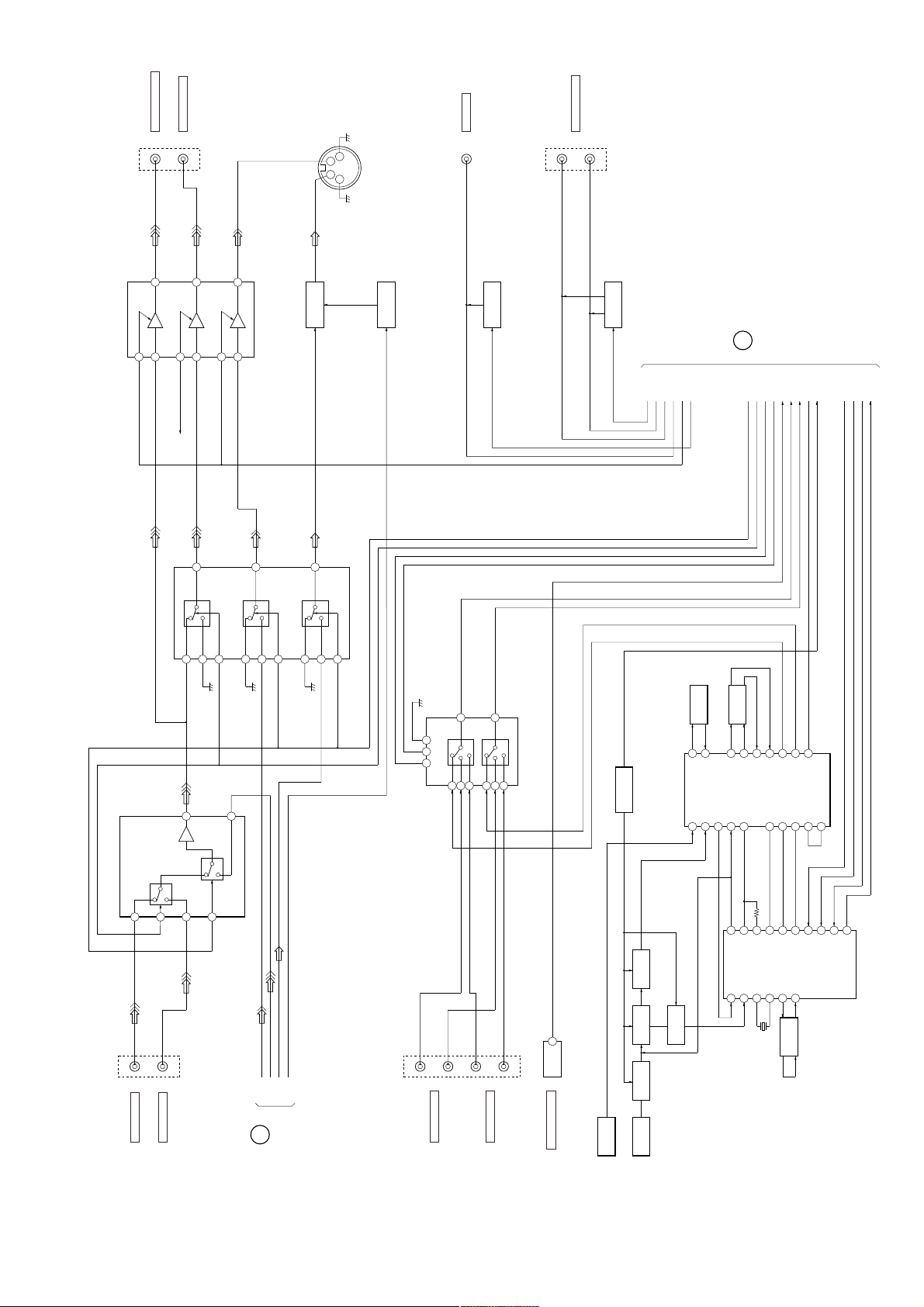
– I/O, TUNER SECTION –
D
VIDEO SECTION
SIGNAL PROCESS/
(Page 23)
AUDIO IN(VIDEO1)
AUDIO IN(VIDEO2)
OPTICAL(DIGITAL IN)
AM
ANTENA
FM
ANTENA
09
MATRIX
D400
POWER,
STANDBY
RM
IC101
LED DRIVER
3
REMOTE
CONTROL RECEIVER
IC100
SI-48
626163
D100-102
FRONT
PANEL
DISPLAY
LCD100
1
48
(LCD)
52
55
LCD
COM 0-3
DRIVER
64
Q100-102
LED DRIVER
Q400-402
SW
S500
ENTER SW
RY361
IC361
POWER AMP
FRONT-L
212623
24
OUTM1(-)
OUTPUT1(+)
OUTPUT2(+)
IN1
IN2
MUTE
131011
KEY2
KEY1
REAR-L
OUTM2(-)
SLEEP
17
EN-A/P A3
EN-B/P A4
STBY-LED
SIRCS
Q401-402,403
SLEEP
G
ON/OFF
FLINH
SECTION
(Page 24)
AUDIO MAIN
IC402
DET AMP
FLDATA
FLCLK
Q405
RELAY SW
6 3
Q403
RELAY ON/OFF
FLCE
DIMI/PA4
DIM2/PA2 NOT USE
09
26 26
C
Q404
SLEEP ON/OFF
RY331
OVER LOAD PROTECTOR
IC401-403,D164,104,134,204,264
OUTPUT1(+)
IC331
POWER AMP
IN1
212623
24
OUTM1(-)
OUTM2(-)
OUTPUT2(+)
IN2
MUTE
SLEEP
131011
17
SW
RY301
IC301
POWER AMP
FRONT-R
212623
24
OUTM1(-)
OUTPUT1(+)
OUTPUT2(+)
IN1
IN2
MUTE
131011
REAR-R
OUTM2(-)
SLEEP
17
HCD-S300
– AMP SECTION – – DISPLAY SECTION –
L
SL
AMP-MUTE
SLEEP/SW-MODE
RLY
FAULT/BTCE1
H
PROTECT/BTCE2
SECTION
(Page 24)
AUDIO MAIN
C
SW
R
SR
09
HCD-S300
I
AUDIO MAIN
SECTION
(Page 24)
+14.5V
D914
EVER+5.6V
31
IC905
REG+5V
2
A+10V
D913
32
1
IC904
REG+10V
Q905
POWER SWITCH
D909
MUTE+5V
M+12V(DVD ON)
D911
D915
D913
Q906
+12V(DVD ON)
Q907
POWER SWITCH
SWITCH
Q909
SWITCH
D916
13
A-10V
32
1
IC903
REG+5V
Q902
POWER SWITCH
IC902
REG+13V
2
Q904
SWITCH
IC908
51
2
REG+3.3V
Q911
Q910
SWITCH
SWITCH
+3.3V(DVD ON:H)
D910
DVD. POWER
POWER
IC907
IC906
REG+5V
REG+5V
D+5V
+5V(DVD ON)
41
2
41
2
Q915
SWITCH
Q913-914
FLIP-FLOP
27 27
T901
POWER TRANSFORMER
D901
MAIN RECTIFIER
LINE
L901
F901
3.15A/125V
AC LINE
LIVE
– POWER SECTION –
FILTER
D907
RECTIFIER
NATURAL
CN 901
D906
RECTIFIER
IC901
OVER CURRENT
REGULATOR
Q903,D921-922
421
VCC
D908
FB/OCP
RECTIFIER
PC901
STARTOR
Q912
SWITCH
09

(Page 30) (Page 30)
28 28
HCD-S300
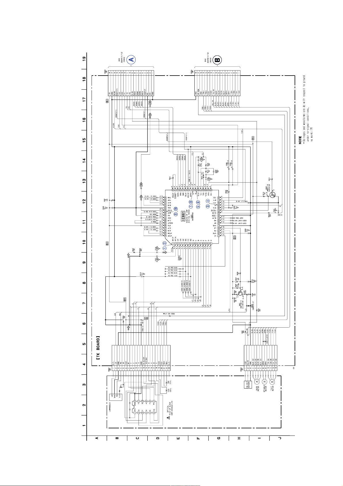
6-3. PRINTED WIRING BOARD – TK SECTION –
• See page 19 for Circuit Boards Location.
HCD-S300
(Page 32)
(Page 32)
29 29
• See page 20 for Waveforms.
6-4. SCHEMATIC DIAGRAM – TK SECTION –
 Loading...