

Page 1
T
T
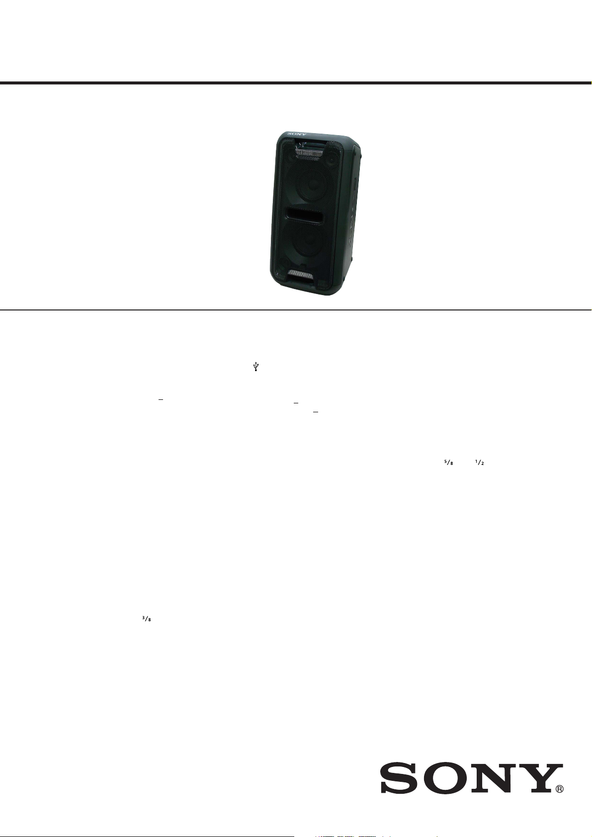
GTK-XB7
SERVICE MANUAL
US Model
Canadian Model
Ver. 1.0 2016.01
SPECIFICATIONS
AUDIO POWER SPECIFICATIONS
POWER OUTPUT AND TOTAL HARMONIC
DISTORTION:
(The United States model only)
Left/Right Channel:
With 3 ohms loads, both channels
driven, from 120
30 watts per channel minimum
RMS power, with no more than
0.7% total harmonic distortion from
250 milliwatts to rated output.
10,000 Hz; rated
Amplier section
he following are measured at
AC 120 V – 240 V, 50/60 Hz
Power Output (rated):
Left/Right Channel: 130 W + 130 W
(at 3 ohms, 1 kHz, 1% THD)
RMS output power (reference):
Left/Right Channel: 235 W + 235 W
(per channel at 3 ohms, 1 kHz, 30%
THD)
Speaker section
Speaker system:
Tweeter + Woofer
weeter L/R:
50 mm (2 in) × 3, cone type
Woofer:
160 mm (6 in) × 2, cone type
Inputs
AUDIO/PARTY CHAIN IN L/R:
Voltage 2 V, impedance 10 kilohms
Outputs
AUDIO/PARTY CHAIN OUT L/R:
Voltage 2 V, impedance 600 ohms
USB section and supported
audio formats
(USB) port:
Type A, maximum current 2.1 A
Supported bit rate:
MP3 (MPEG1 Audio Layer-3):
32 kbps
320 kbps, VBR
WMA: 32 kbps
Sampling frequencies:
MP3 (MPEG1 Audio Layer-3):
32/44.1/48 kHz
WMA: 44.1 kHz
192 kbps, VBR
BLUETOOTH section
Communication system:
BLUETOOTH Standard version 3.0
Output:
BLUETOOTH Standard Power Class 2
Maximum communication range:
Line of sight approx. 10 m (33 feet)
Frequency band:
2.4 GHz band (2.4000 GHz –
2.4835 GHz)
Modulation method:
FHSS (Freq Hopping Spread
Spectrum)
Compatible BLUETOOTH profiles
A2DP (Advanced Audio Distribution
Profile)
AVRCP (Audio Video Remote Control
Profile)
SPP (Serial Port Profile)
Supported codecs:
SBC (Sub Band Codec)
AAC (Advanced Audio Coding)
LDAC
1)
The actual range will vary depending
on factors such as obstacles between
devices, magnetic fields around a
microwave oven, static electricity,
reception sensitivity, antenna’s
performance, operating system, software
application, etc.
2)
BLUETOOTH standard profiles indicate the
purpose of BLUETOOTH communication
between devices.
2)
:
General
Power requirements:
AC 120 V, 60 Hz
Power consumption:
60 W
Standby power consumption:
When BLUETOOTH standby mode is
set to off: 0.5 W (eco mode)
When BLUETOOTH standby mode is
set to on: 2.8 W (all wireless network
ports on)
Dimensions (W/H/D) (Approx.):
330 mm × 650 mm × 340 mm (13 in
× 25 in × 13 in)
Mass (Approx.):
12 kg (26 lb 16 oz)
Quantity of the system:
1 piece
Supplied accessories:
1)
Remote control (1)
R03 (size AAA) batteries (2)
AC power cord (1)
Design and specifications are subject to
change without notice.
HOME AUDIO SYSTEM
9-896-261-01
2016A33-1
2016.01
©
Sony Video & Sound Products Inc.
Published by Sony Techno Create Corporation
Page 2
GTK-XB7
License and Trademark
Notice
s MPEG Layer-3 audio cAoding
technology and patents licensed
from Fraunhofer IIS and Thomson.
s Windows Media is either a registered
trademark or trademark of Microsoft
Corporation in the United States
and/or other countries.
s This product is protected by
certain intellectual property rights
of Microsoft Corporation. Use or
distribution of such technology
outside of this product is prohibited
without a license from Microsoft or
an authorized Microsoft subsidiary.
s The BLUETOOTH® word mark and
logos are registered trademarks
owned by Bluetooth SIG, Inc. and
any use of such marks by Sony
Corporation is under license. Other
trademarks and trade names are
those of their respective owners.
s The N Mark is a trademark or
registered trademark of NFC Forum,
Inc. in the United States and in other
countries.
s Android™ is a trademark of Google
Inc.
s Google Play™ is a trademark of
Google Inc.
s LDAC™ and LDAC logo are
trademarks of Sony Corporation.
s Apple, the Apple logo, iPad, iPhone,
and iPod touch are trademarks of
Apple Inc., registered in the U.S. and
other countries. iPad Air and iPad
mini are trademarks of Apple Inc.
App Store is a service mark of Apple
Inc.
s “Made for iPod,” “Made for
iPhone,” “Made for iPad” mean
that an electronic accessory
has been designed to connect
specifically to iPod , iPhone, or iPad
respectively, and has been certified
by the developer to meet Apple
performance standards. Apple is not
responsible for the operation of this
device or its compliance with safety
and regulatory standards. Please
note that the use of this accessory
with iPod, iPhone, or iPad may affect
wireless performance.
s All other trademarks and registered
trademarks are of their respective
holders. In this manual,
marks are not specified.
TM
and
®
SAFETY CHECK-OUT
After correcting the original service problem, perform the following safety check before releasing the set to the customer:
Check the antenna terminals, metal trim, “metallized” knobs,
screws, and all other exposed metal parts for AC leakage.
Check leakage as described below.
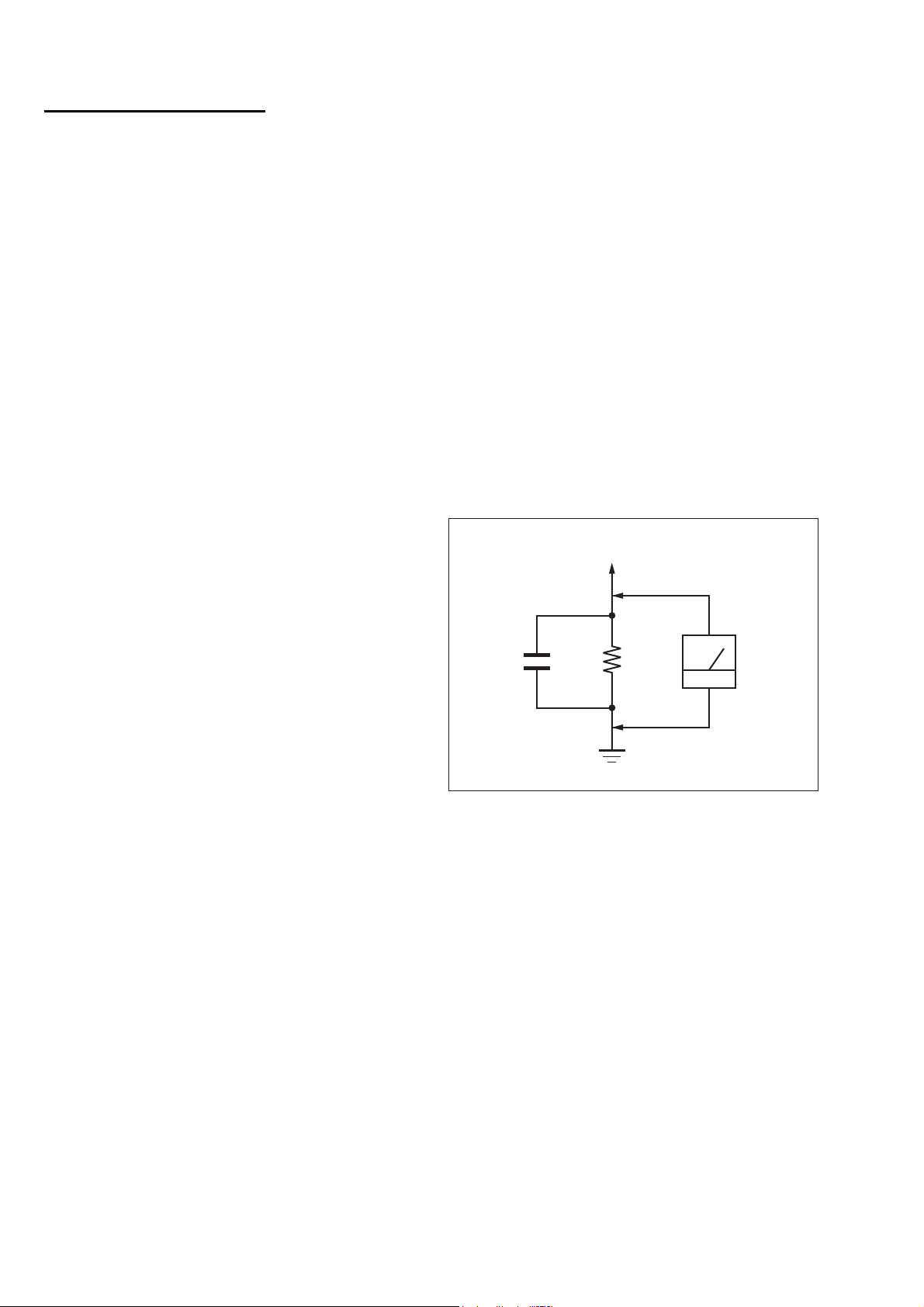
LEAKAGE TEST
The AC leakage from any exposed metal part to earth ground and
from all exposed metal parts to any exposed metal part having a
return to chassis, must not exceed 0.5 mA (500 microamperes.).
Leakage current can be measured by any one of three methods.
1. A commercial leakage tester, such as the Simpson 229 or RCA
WT-540A. Follow the manufacturers’ instructions to use these
instruments.
2. A battery-operated AC milliammeter. The Data Precision 245
digital multimeter is suitable for this job.
3. Measuring the voltage drop across a resistor by means of a
VOM or battery-operated AC voltmeter. The “limit” indication
is 0.75 V, so analog meters must have an accurate low-voltage
scale. The Simpson 250 and Sanwa SH-63Trd are examples
of a passive VOM that is suitable. Nearly all battery operated
digital multimeters that have a 2 V AC range are suitable. (See
Fig. A)
To Exposed Metal
Parts on Set
AC
1.5 kΩ0.15 μF
Earth Ground
voltmeter
(0.75 V)
Fig. A. Using an AC voltmeter to check AC leakage.
SAFETY-RELATED COMPONENT WARNING!
COMPONENTS IDENTIFIED BY MARK 0 OR DOTTED LINE
WITH MARK 0 ON THE SCHEMATIC DIAGRAMS AND IN
THE PARTS LIST ARE CRITICAL TO SAFE OPERATION.
REPLACE THESE COMPONENTS WITH SONY PARTS
WHOSE PART NUMBERS APPEAR AS SHOWN IN THIS
MANUAL OR IN SUPPLEMENTS PUBLISHED BY SONY.
ATTENTION AU COMPOSANT AYANT RAPPORT
LES COMPOSANTS IDENTIFIÉS PAR UNE MARQUE 0 SUR
LES DIAGRAMMES SCHÉMATIQUES ET LA LISTE DES
PIÈCES SONT CRITIQUES POUR LA SÉCURITÉ DE FONCTIONNEMENT. NE REMPLACER CES COMPOSANTS QUE
PAR DES PIÈCES SONY DONT LES NUMÉROS SONT DONNÉS DANS CE MANUEL OU DANS LES SUPPLÉMENTS
PUBLIÉS PAR SONY.
À LA SÉCURITÉ!
2
Page 3

TABLE OF CONTENTS
GTK-XB7
1. SERVICING NOTES ............................................. 4
2. DISASSEMBLY
2-1. Disassembly Flow ........................................................... 5
2-2. Top Cover Block ............................................................. 6
2-3. Fan Unit (M1) ................................................................. 7
2-4. PSU Board ...................................................................... 7
2-5. MAIN Board ................................................................... 8
2-6. USB + KEY Board .......................................................... 9
2-7. BT&NFC Board .............................................................. 9
2-8. CONTROL Board ........................................................... 10
2-9. Side Panel (R), Side Panel (L) ........................................ 11
2-10. Main Chassis Block ........................................................ 12
2-11. Bottom Cover + Plate ..................................................... 13
2-12. Front Panel Block ........................................................... 14
2-13. LB Board ......................................................................... 15
2-14. LA Board ......................................................................... 16
2-15. RGBF Board ................................................................... 17
2-16. RGBE Board ................................................................... 17
2-17. IR Board .......................................................................... 18
2-18. Tweeter (SP5).................................................................. 18
2-19. Tweeter (SP3, SP4) ......................................................... 19
2-20. Woofer (SP1, SP2) .......................................................... 20
3. TEST MODE ............................................................ 21
4. DIAGRAMS
4-1. Block Diagram - OVERALL Section - ........................... 23
4-2. Block Diagram - POWER SUPPLY Section - ................ 24
4-3. Printed Wiring Board - MAIN Board - ........................... 25
4-4. Schematic Diagram - MAIN Board (1/8) - ..................... 26
4-5. Schematic Diagram - MAIN Board (2/8) - ..................... 27
4-6. Schematic Diagram - MAIN Board (3/8) - ..................... 28
4-7. Schematic Diagram - MAIN Board (4/8) - ..................... 29
4-8. Schematic Diagram - MAIN Board (5/8) - ..................... 30
4-9. Schematic Diagram - MAIN Board (6/8) - ..................... 31
4-10. Schematic Diagram - MAIN Board (7/8) - ..................... 32
4-11. Schematic Diagram - MAIN Board (8/8) - ..................... 33
4-12. Printed Wiring Board - BT&NFC Board - ...................... 34
4-13. Schematic Diagram - BT&NFC Board - ........................ 34
4-14. Printed Wiring Board - USB + KEY Board - ................. 35
4-15. Schematic Diagram - USB + KEY Board - .................... 35
4-16. Printed Wiring Board - IR Board - .................................. 35
4-17. Schematic Diagram - IR Board - .................................... 35
4-18. Printed Wiring Board - CONTROL Board - ................... 36
4-19. Schematic Diagram - CONTROL Board - ...................... 37
4-20. Printed Wiring Board - LA Board - ................................ 38
4-21. Printed Wiring Board - RGBE Board - ........................... 38
4-22. Schematic Diagram - LA Board - ................................... 39
4-23. Schematic Diagram - RGBE Board - .............................. 39
4-24. Printed Wiring Board - LB Board - ................................ 40
4-25. Printed Wiring Board - RGBF Board - ........................... 40
4-26. Schematic Diagram - LB Board - ................................... 41
4-27. Schematic Diagram - RGBF Board - .............................. 41
4-28. Printed Wiring Board - PSU Board - .............................. 42
4-29. Schematic Diagram - PSU Board - ................................. 43
5. EXPLODED VIEWS
5-1. Side Panel Section .......................................................... 49
5-2. Cabinet Section ............................................................... 50
5-3. Top Cover Section........................................................... 51
5-4. MAIN Board Section ...................................................... 52
5-5. Front Panel Section ......................................................... 53
6. ACCESSORIES ....................................................... 54
3
Page 4

GTK-XB7
SECTION 1
SERVICING NOTES
The SERVICING NOTES contains important information for servicing. Be sure to read this section before repairing the unit.
UNLEADED SOLDER
Boards requiring use of unleaded solder are printed with the leadfree mark (LF) indicating the solder contains no lead.
(Caution: Some printed circuit boards may not come printed with
the lead free mark due to their particular size)
: LEAD FREE MARK
Unleaded solder has the following characteristics.
• Unleaded solder melts at a temperature about 40 °C higher
than ordinary solder.
Ordinary soldering irons can be used but the iron tip has to be
applied to the solder joint for a slightly longer time.
Soldering irons using a temperature regulator should be set to
about 350 °C.
Caution: The printed pattern (copper foil) may peel away if
the heated tip is applied for too long, so be careful!
• Strong viscosity
Unleaded solder is more viscous (sticky, less prone to fl ow)
than ordinary solder so use caution not to let solder bridges
occur such as on IC pins, etc.
• Usable with ordinary solder
It is best to use only unleaded solder but unleaded solder may
also be added to ordinary solder.
REPAIRING THE BOARDS
When each boards installed in this unit are defective, replace the
mounted board.
Individual electrical parts that mounted on the each boards cannot
be replaced.
Printed wiring board and schematic diagram that have been described on this service manual are for reference.
4
Page 5
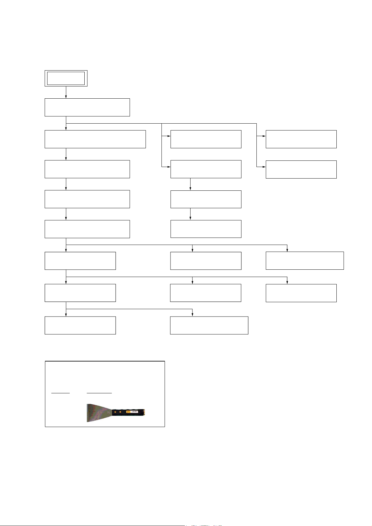
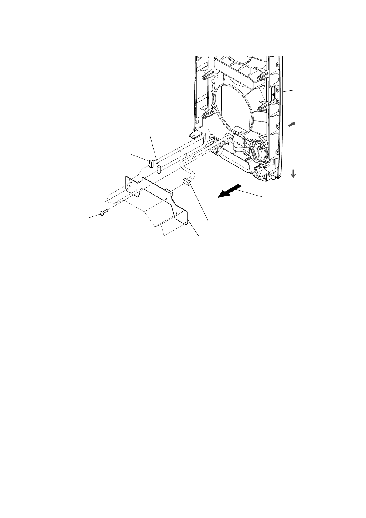
DISASSEMBLY
• This set can be disassembled in the order shown below.
2-1. DISASSEMBLY FLOW
SET
2-2. TOP COVER BLOCK
(Page 6)
GTK-XB7
SECTION 2
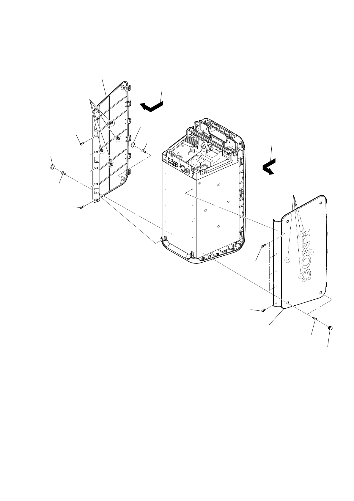
2-9. SIDE PANEL (R), SIDE PANEL (L)
(Page 11)
2-10. MAIN CHASSIS BLOCK
(Page 12)
2-11. BOTTOM COVER + PLATE
(Page 13)
2-12. FRONT PANEL BLOCK
(Page 14)
2-13. LB BOARD
(Page 15)
2-14. LA BOARD
(Page 16)
2-3. FAN UNIT (M1)
(Page 7)
2-4. PSU BOARD
(Page 7)
2-5. MAIN BOARD
(Page 8)
2-6. USB + KEY BOARD
(Page 9)
2-17. IR BOARD
(Page 18)
2-15. RGBF BOARD
(Page 17)
2-7. BT&NFC BOARD
(Page 9)
2-8. CONTROL BOARD
(Page 10)
2-20. WOOFER (SP1, SP2)
(Page 20)
2-18. TWEETER (SP5)
(Page 18)
2-16. RGBE BOARD
(Page 17)
JIG
When disassembling the unit, use the following
jig for speaker removal.
Part No. Description
J-2501-238-A JIG FOR SPEAKER REMOVAL
2-19. TWEETER (SP3, SP4)
(Page 19)
5
Page 6
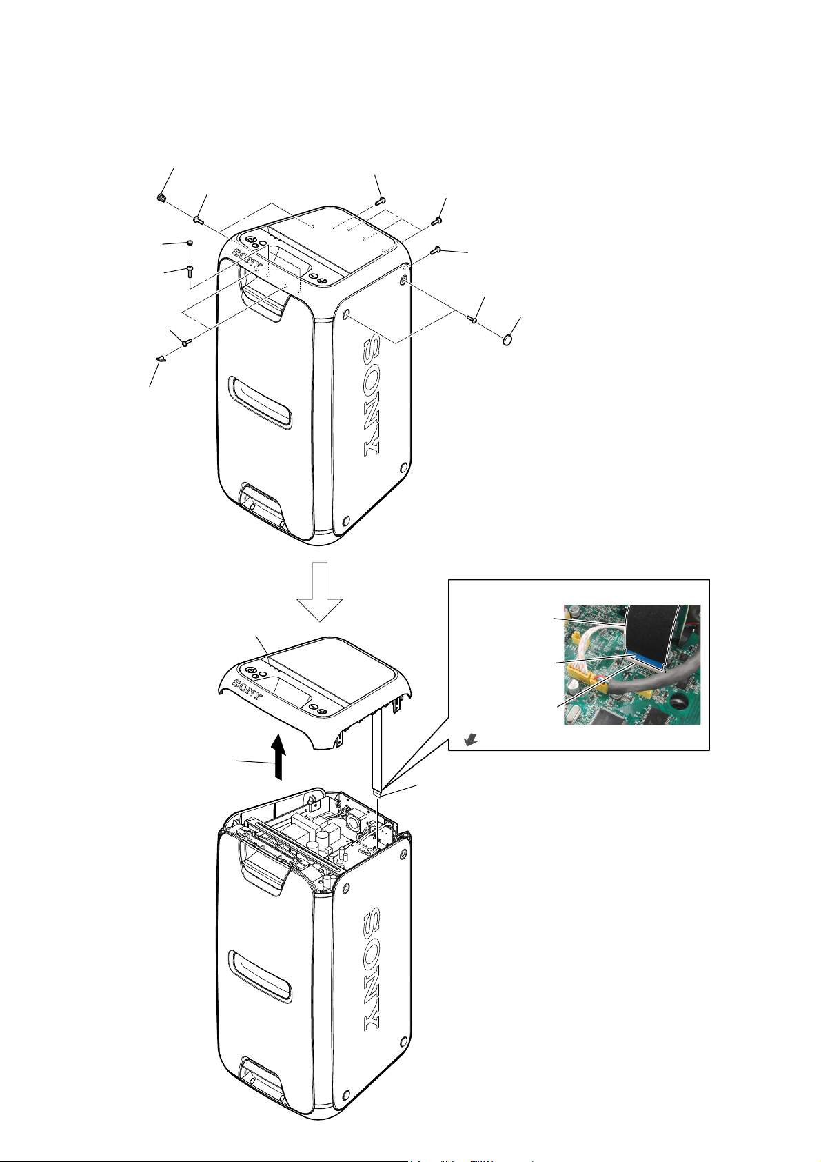
GTK-XB7
Note: Follow the disassembly procedure in the numerical order given.
2-2. TOP COVER BLOCK
5 two rubber
(small circle)
6 two screws
8 two screws
7 two rubber (square)
2 two rubber (circle)
3 two screws
3 screw
4 three screws
3 screw
3 two screws
1 two rubber (large circle)
qa top cover block
9 Remove the top cover block
in the direction of the arrow.
)OH[LEOHIODWFDEOH))&WR0$,1VHWWLQJ
flexible flat cable
(FFC (to MAIN))
The opposite side is
the terminal side.
XP35
front side
0 flexible flat cable (FFC (to MAIN))
(XP35)
6
Page 7
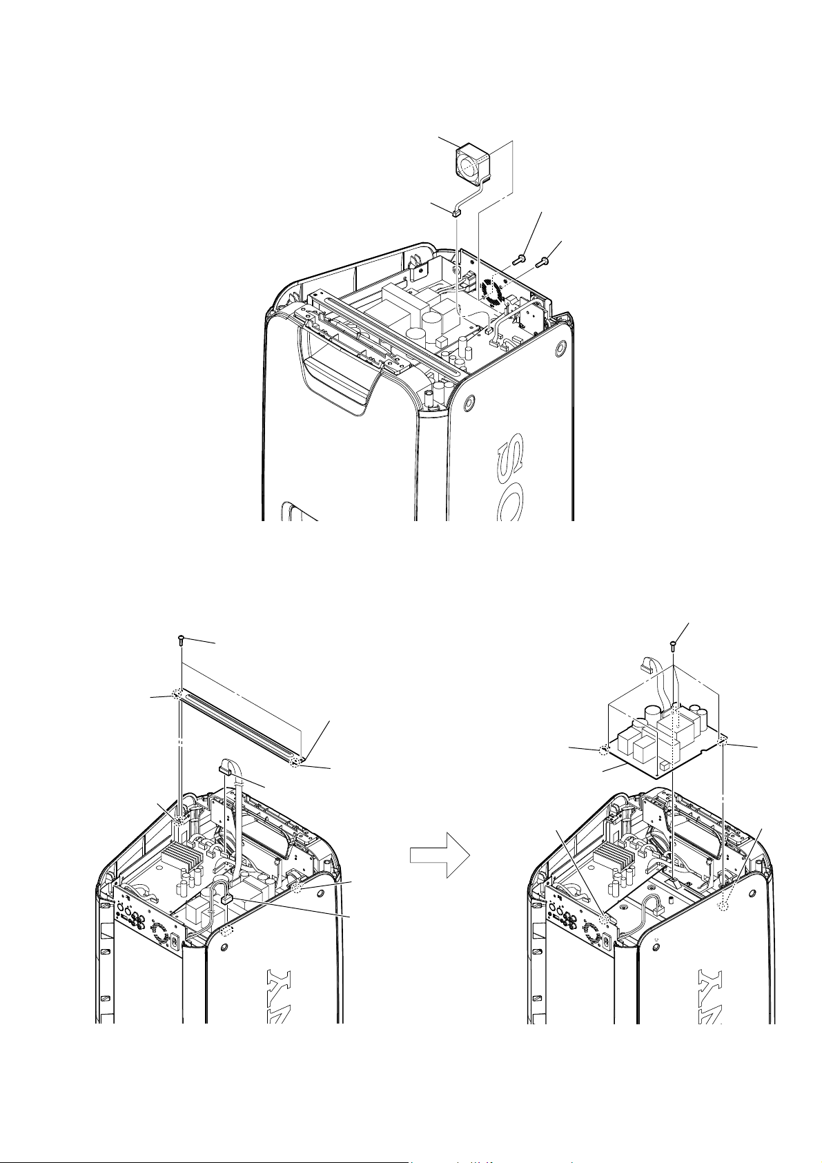
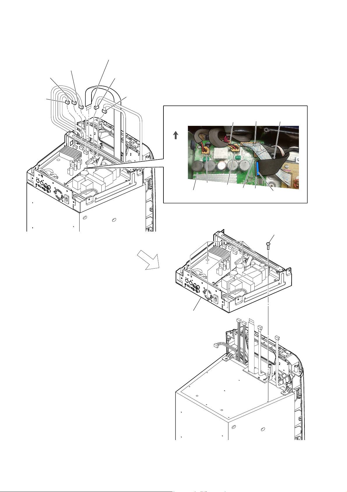
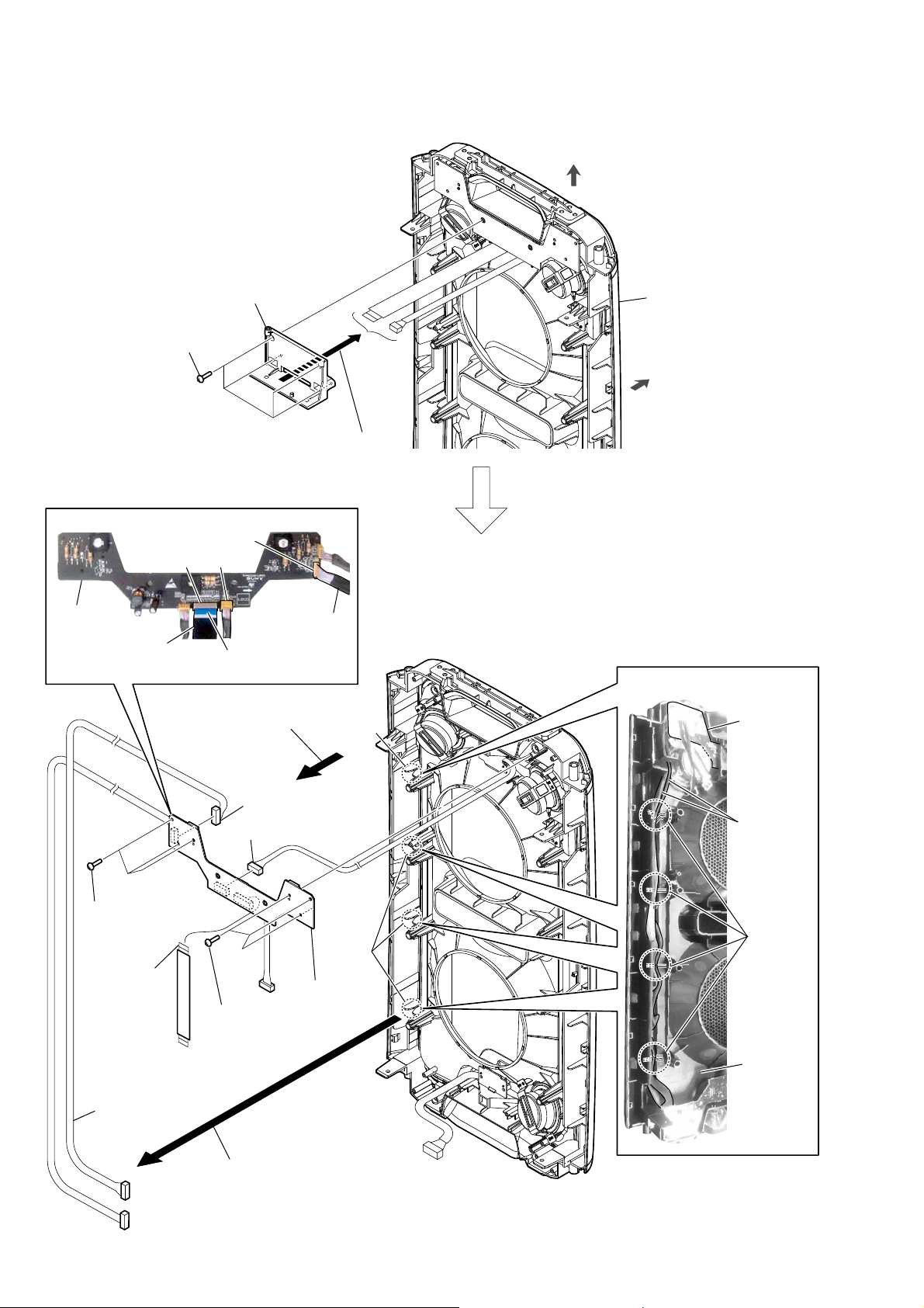
2-3. FAN UNIT (M1)
GTK-XB7
3 fan unit (M1)
2-4. PSU BOARD
1 connector (XP14)
2 screw
2 screw
hole
boss
1 two screws
3 connector (XP1)
2 reinforcement bracket
hole
boss
4 connector
(CN501)
ditch
6 PSU board
boss
5 five screws
hole
boss
– Rear view –
7
Page 8
GTK-XB7
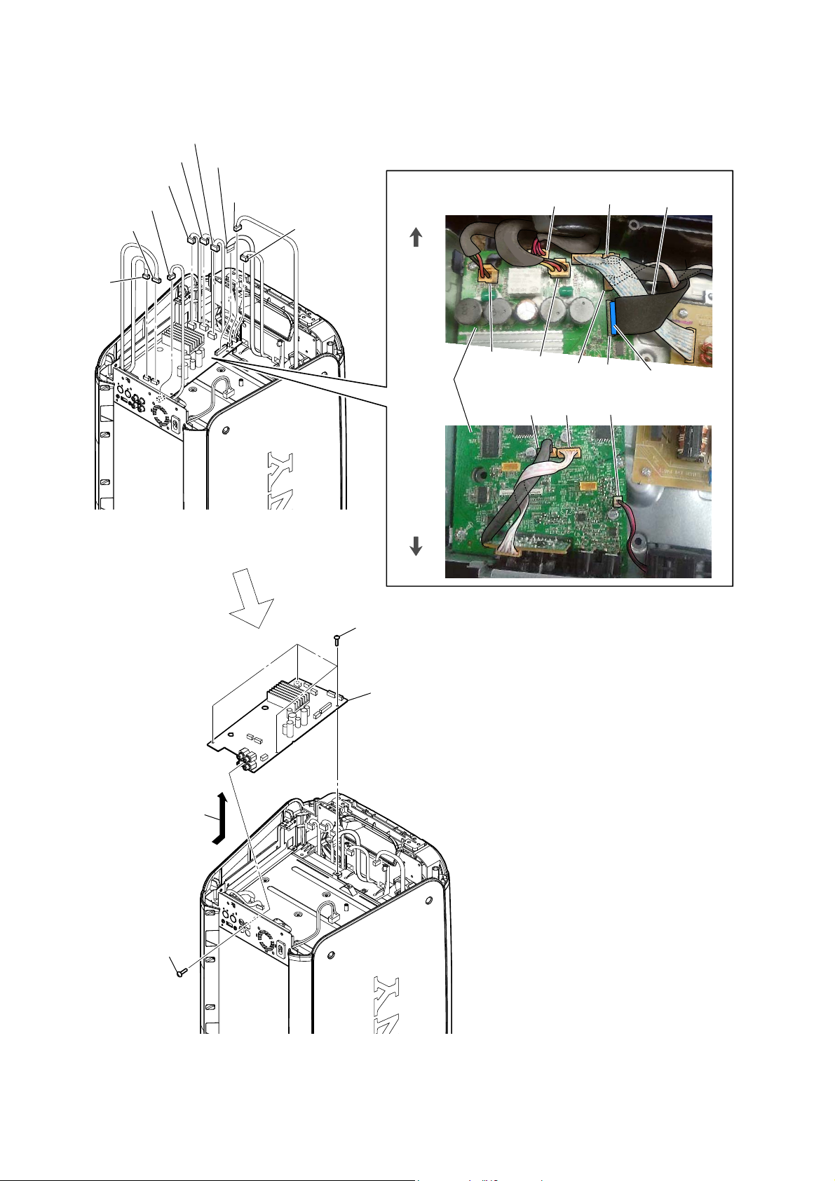
2-5. MAIN BOARD
5 connector (XP10)
4 connector (XP21)
3 connector (XP14)
2 connector (XP7)
1 connector
(XP37)
6 connector (XP22)
7 flexible flat cable
(XP45)
8 connector (XP36)
9 connector
(XP25)
:LUHVHWWLQJ
front side
XP10 XP25
flexible flat cable
– Rear view –
MAIN board
rear side
qa four screws
qd MAIN board
XP21
XP22
XP37 XP7 XP14
XP36
XP45
The opposite side is
the terminal side.
qs Remove the MAIN board in
the direction of the arrow.
0 screw
8
Page 9
2-6. USB + KEY BOARD
GTK-XB7
2 USB + KEY board
1 three screws
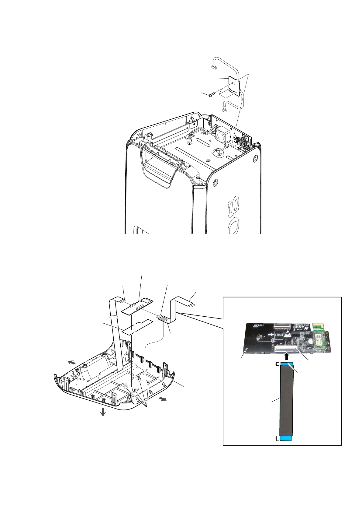
2-7. BT&NFC BOARD
4 flexible flat cable (FFC (to BT&NFC))
(XP8)
5 BT board adhesive sheet
front side
top side
6 BT&NFC board
1 connector
(XP34)
2 Peel off the
adhesive sheet.
rear side
claw
3 flexible flat cable (to MAIN)
)OH[LEOHIODWFDEOHWR0$,1VHWWLQJ
Note:
to the BT&NFC board.
BT&NFC board
top cover block
Connect the side of short reinforcement plate
short
flexible flat cable
(to MAIN)
XP34
The opposite side is
the terminal side.
long
9
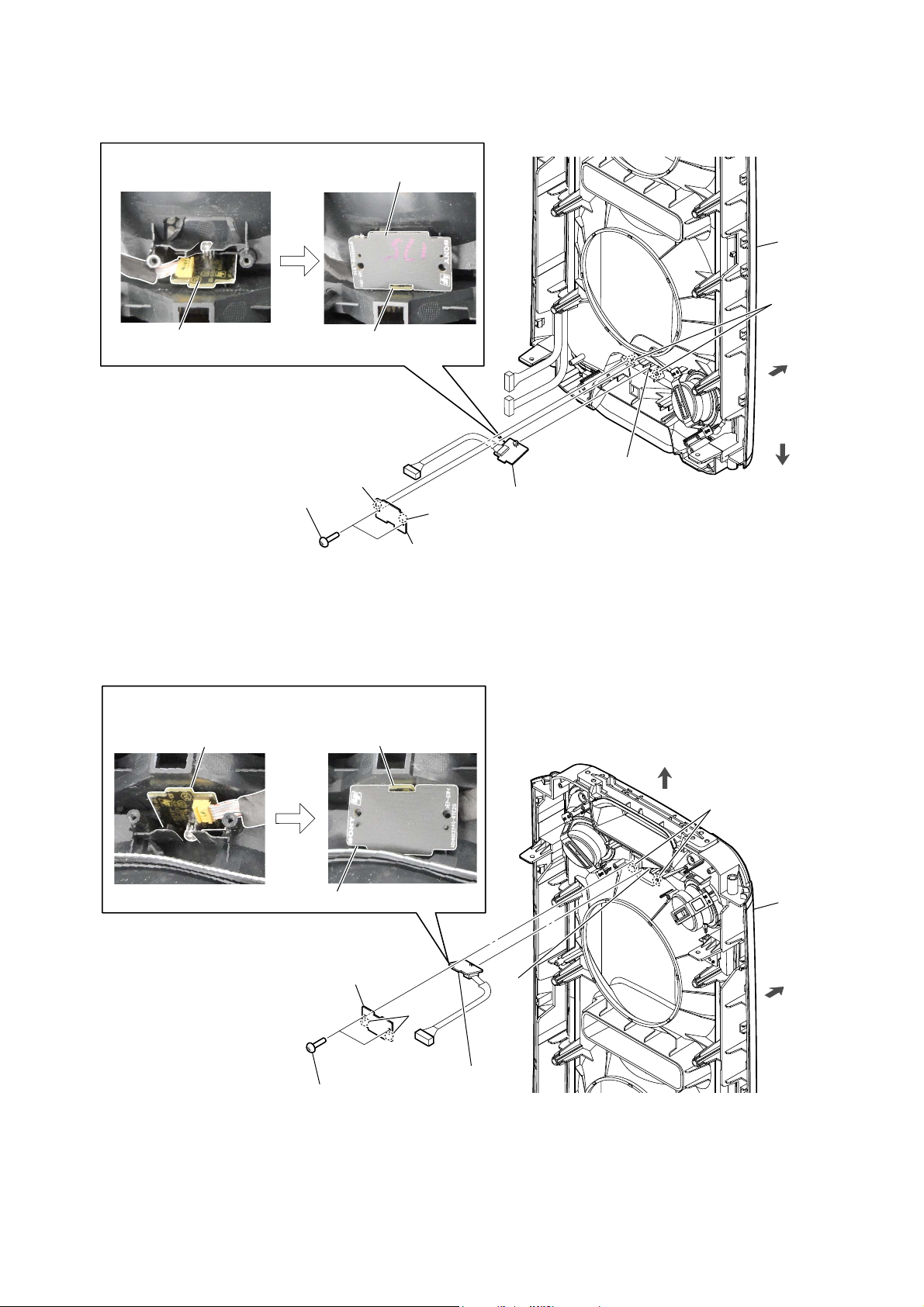
Page 10
GTK-XB7
2-8. CONTROL BOARD
6 CONTROL board
4 Remove the CONTROL board block
in the direction of the arrow.
2 eight screws
3 plate
5 flexible flat cable (FFC (to BT&NFC))
(XP16)
The opposite side is the terminal side.
1 connector
(XP8)
front side
top side
top cover block
rear side
10
Page 11
2-9. SIDE PANEL (R), SIDE PANEL (L)
GTK-XB7
5 side panel (R)
Note:
remove the used bond and use a new
bond to fix the side panel (R).
1 rubber (large circle)
When installing t
3 four screws
2 screw
3 screw
he side panel (R),
bond
4 Remove the side panel (R)
in the direction of the arrow.
1 rubber
(large circle)
2 screw
4 Remove the side panel (L)
in the direction of the arrow.
bond
– Rear view –
5 side panel (L)
Note:
remove the used bond and use a new
bond to fix the side panel (L).
3 screw
When installing t
3 four screws
he side panel (L),
2 two screws
1 two rubber (circle)
11
Page 12
GTK-XB7
2-10. MAIN CHASSIS BLOCK
2 connector
(XP10)
1 connector
(XP21)
3 connector
(XP22)
4 flexible flat cable
(XP45)
5 connector
(XP36)
6 connector
(XP25)
:LUHVHWWLQJ
front side
MAIN board
XP21
XP10 XP25
XP22
XP36
flexible flat cable
XP45
The opposite side is
the terminal side.
– Rear view –
7 seven screws
8 main chassis block
12
Page 13
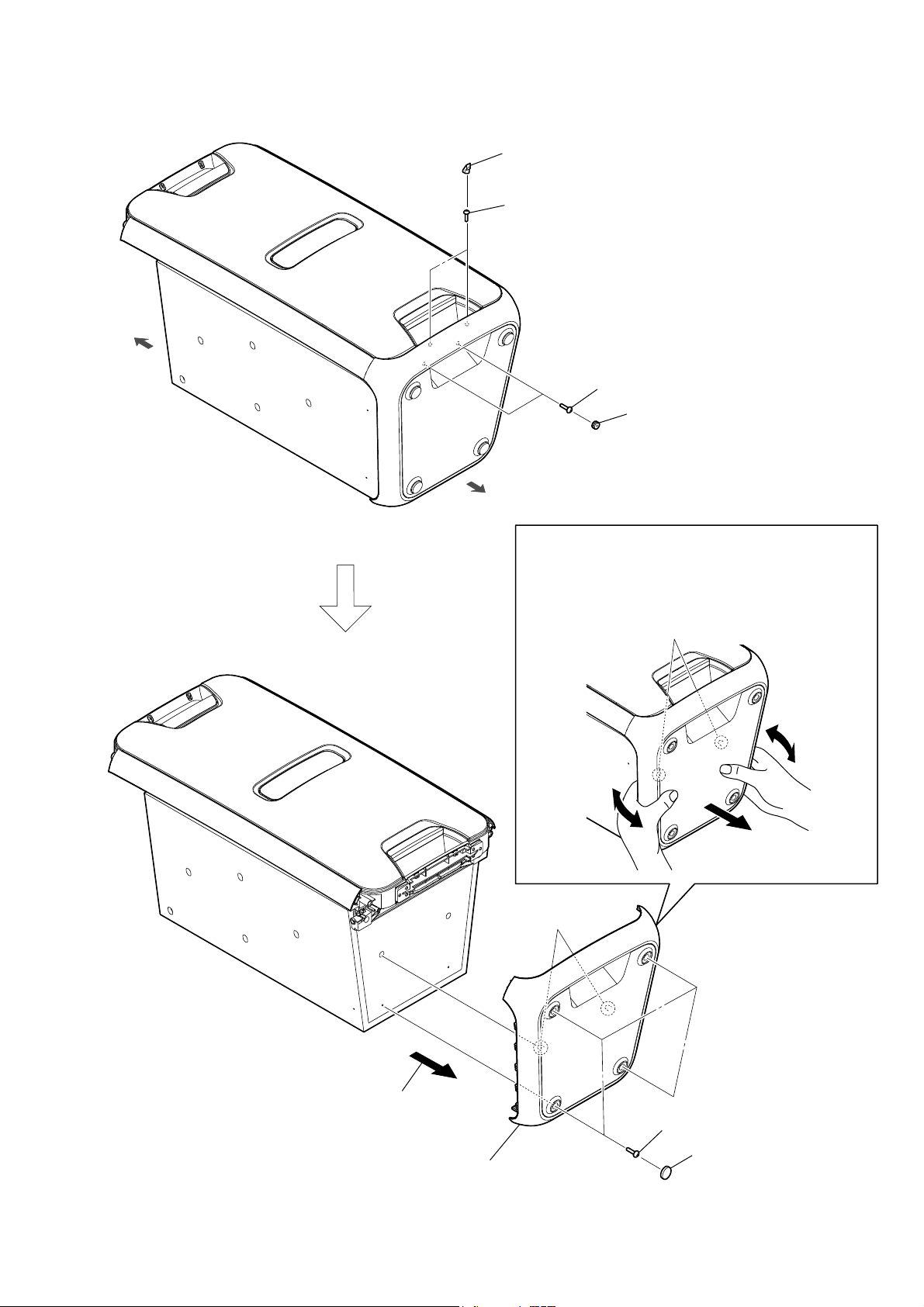
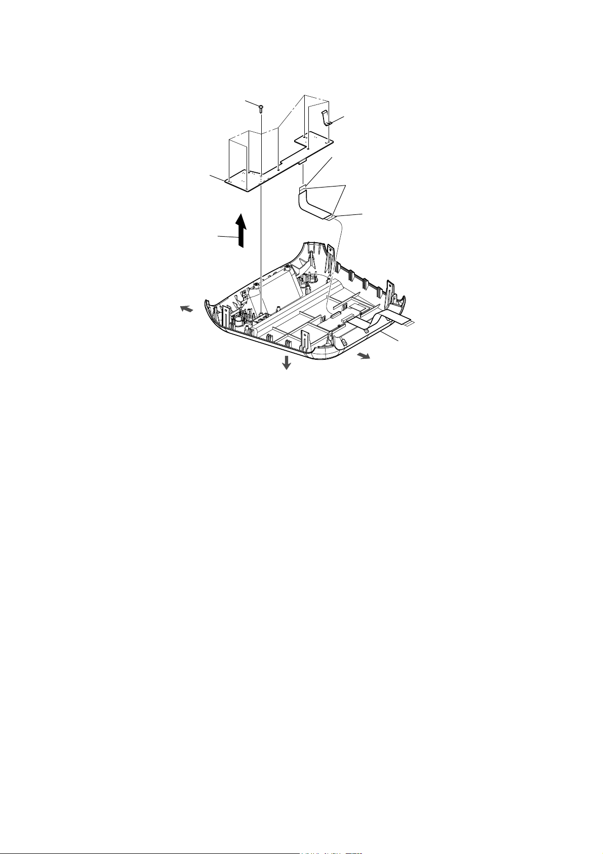
2-11. BOTTOM COVER + PLATE
top side
GTK-XB7
1 two rubber (square)
2 two screws
4 two screws
3 two rubber (small circle)
bottom side
+RZWRUHPRYHWKHERWWRPFRYHUSODWH
Note 1:
cover + plate slowly and remove the bond as shown figure.
Note 2:
carefully so as not to damage the bosses.
When removing the bottom cover + plate, move the bottom
When removing the bottom cover + plate, please remove
two bosses
bond
7 Remove the bottom cover + plate
in the direction of the arrow.
8 bottom cover + plate
Note 3:
remove the used bond and use a new
bond to fix the bottom cover + plate.
When installing the
6 four screws
5 four rubber (large circle)
bottom cover + plate,
13
Page 14
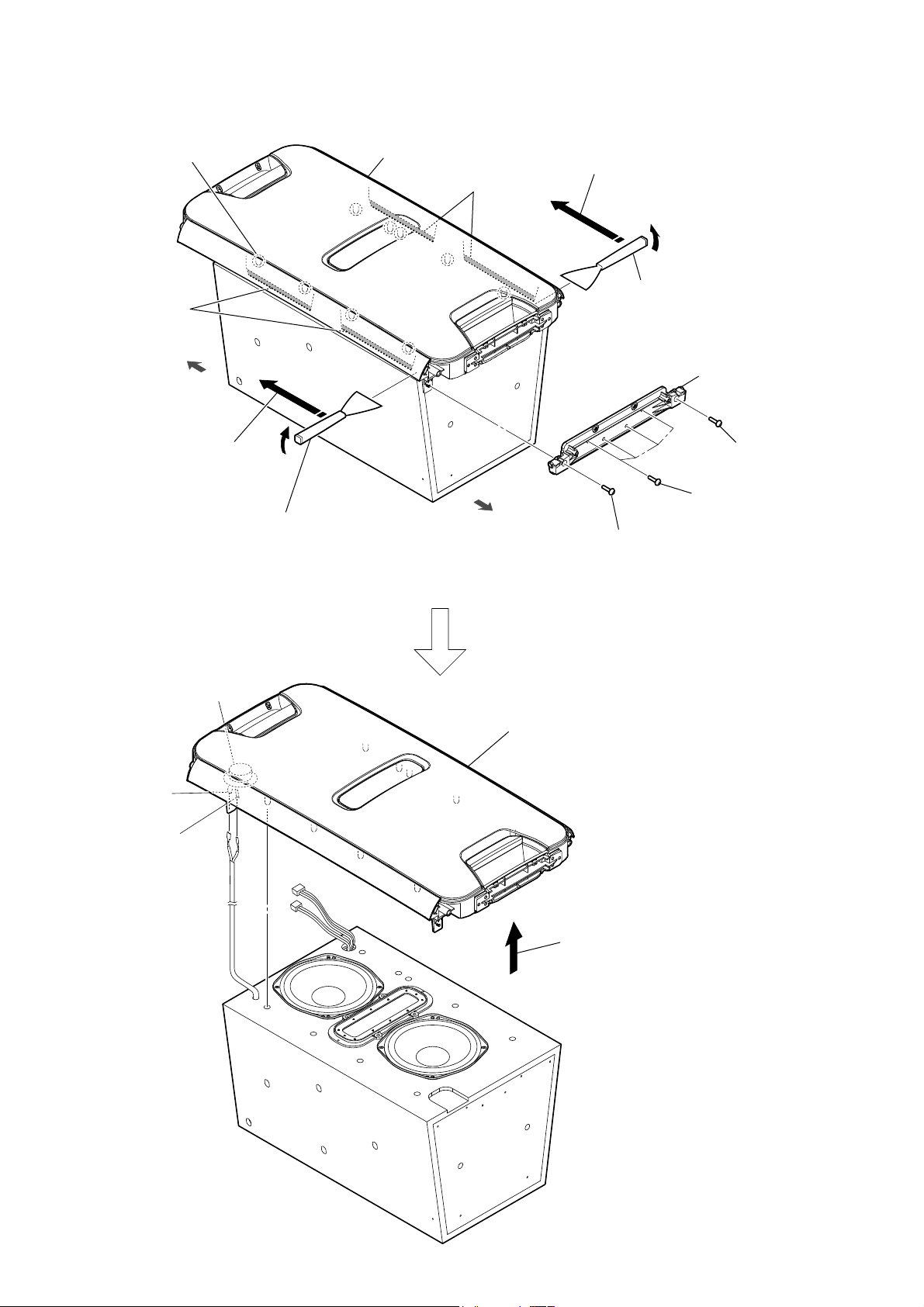
GTK-XB7
2-12. FRONT PANEL BLOCK
total nine bosses
cushion
top side
5 All bosses are removed while moving
jig in the direction of the arrow, and
front panel block is removed.
4 Insert the jig into a space and raise
front panel block.
Note 1: When using a jig, please work
so as not to injure the cushion.
front panel block
cushion
5 All bosses are removed while moving
jig in the direction of the arrow, and
front panel block is removed.
4 Insert the jig into a space and raise
front panel block.
Note 1: When using a jig, please work
so as not to injure the cushion.
3 prop (bottom)
1 screw
2 four screws
bottom side
1 screw
speaker unit (TW) (SP4)
7 tweeter terminal
(wide side)
7 tweeter terminal
(narrow side)
8 front panel block
Note 2:
remove the used bond and use a new
bond to fix the front panel block.
When installing the
6 Remove the front panel block
in the direction of the arrow.
front panel block
14
Page 15
2-13. LB BOARD
3 connector (XP56)
GTK-XB7
front panel block
front side
4 connector (XP37)
bottom side
1 eight screws
2 Remove the LB board block
in the direction of the arrow.
5 connector (XP50)
6 LB board
15
Page 16
GTK-XB7
2-14. LA BOARD
top side
1 four screws
:LUHVHWWLQJ
LA board
flexible flat cable
3 prop (upper)
XP55
XP54
XP38
The opposite side is
–)URQWYLHZ–
5 Remove the LA board block
in the direction of the arrow.
the terminal side.
2 Draw two cables
out from the hole.
cable
groove
front panel block
front side
:LUHVHWWLQJ
LA board
4 three screws
6 flexible flat
cable
(XP38)
0 cable
8 connector (XP55)
7 connector (XP54)
groove
qa LA board
4 three screws
9 Remove two cables from four
grooves of the front panel.
two cables
groove
front panel
block
16
Page 17
2-15. RGBF BOARD
GTK-XB7
+RZWRLQVWDOOWKH5*%)ERDUG
Install the RGBF board
into the slot.
1 two screws
mounting plate (bottom right)
Make sure that the projection
of the RGBF board is out.
hole
hole
2 mounting plate (bottom right)
3 RGBF board
slot
front panel block
boss
front side
bottom side
2-16. RGBE BOARD
+RZWRLQVWDOOWKH5*%(ERDUG
Install the RGBE board
into the slot.
– Rear bottom view –
Make sure that the projection
of the RGBE board is out.
mounting plate (bottom left)
2 mounting plate
(bottom left)
1 two screws
hole
3 RGBE board
slot
top side
boss
front panel block
front side
17
Page 18

GTK-XB7
2-17. IR BOARD
top side
3 flannel
2 IR board
front panel block
2-18. TWEETER (SP5)
front side
1 screw
front panel block
18
2 speaker plate
1 two screws
front side
bottom side
3 tweeter terminal
(wide side)
3 tweeter terminal
(narrow side)
4 speaker unit (TW) (SP5)
Page 19

2-19. TWEETER (SP3, SP4)
2 speaker plate
GTK-XB7
top side
front panel block
4 speaker unit (TW)
(SP3)
front side
3 tweeter terminal
(wide side)
1 two screws
3 tweeter terminal
(narrow side)
7 speaker unit (TW)
(SP4)
6 speaker plate
5 two screws
19
Page 20
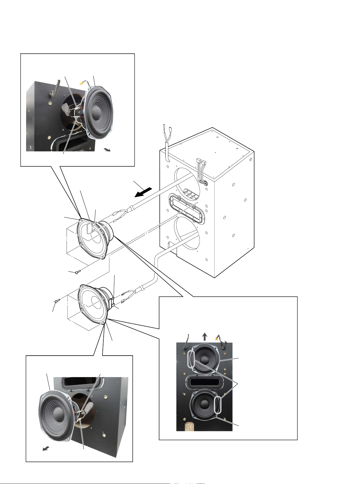
GTK-XB7
2-20. WOOFER (SP1, SP2)
:LUHVHWWLQJ
woofer terminal
(wide side)
speaker unit (WF) (SP2)
woofer terminal
(narrow side)
4 speaker unit (WF)
(SP2)
1 four screws
1 four screws
front side
2 Remove the speaker unit (WF)
in the direction of the arrow.
3 woofer terminal
(narrow side)
3 woofer terminal
(wide side)
3 woofer terminal
(narrow side)
3 woofer terminal
(wide side)
,QVWDOODWLRQGLUHFWLRQIRUWKHVSHDNHUXQLW:)6363
When installing the speaker unit (WF) (SP1), (SP2), make
Note:
sure that there is a position of the speaker terminal to the
position shown in the figure below.
top side
20
:LUHVHWWLQJ
speaker unit (WF) (SP1)
front side
woofer terminal
(wide side)
4 speaker unit (WF)
(SP1)
speaker unit (WF) (SP2)
woofer terminal
(narrow side)
terminals position
speaker unit (WF) (SP1)
–)URQWYLHZ–
Page 21

SECTION 3
TEST MODE
SOFTWARE VERSION DISPLAY
It can confi rm the software version.
Procedure:
1. Press the [
2. Press the [FUNCTION] button to select the AUDIO IN function.
3. Press the button on the remote commander as following order.
[>] → [EXTRA BASS] → [.]
4. Each software versions are shown by the blinking frequency of
LEDs simultaneously.
Example:
When the MCU version is “v15”, the [
[EXTRA BASS] LED blinks 5 times.
When the MPEG version is “v07”, the [AUDIO IN] LED blinks 0
time, the [USB] LED blinks 7 times.
When the BT version is “v075”, the [SPEAKER ADD L] LED
blinks 0 time, the [SPEAKER ADD R] LED blinks 7 times, the
[PARTY CHAIN] LED blinks 5 times.
FACTORY RESET
It can reset all MPEG settings and clear the Bluetooth linked list.
Execute this mode when returning the this unit to the customer.
] button to turn the power on.
1
] LED blinks 1 time, the
1
GTK-XB7
Procedure:
1. Press the [1] button to turn the power on.
2. Press two buttons of the [FUNCTION] and [–] simultaneously
for 5 seconds.
3. The [1] LED blinks for 3 seconds, and then reboot the system.
21
Page 22

GTK-XB7
MEMO
MEMO
22
Page 23

4-1. BLOCK DIAGRAM - OVERALL Section -
GTK-XB7
SECTION 4
DIAGRAMS
GTK-XB7
2323
Page 24

GTK-XB7
d
4-2. BLOCK DIAGRAM - POWER SUPPLY Section -
THIS NOTE IS COMMON FOR PRINTED WIRING BOARDS AND SCHEMATIC DIAGRAMS.
(In addition to this, the necessary note is printed in each block.)
For Printed Wiring Boards.
Note:
• : Pattern from the side which enables seeing.
(The other layers’ patterns are not indicated.)
Caution:
Pattern face side:
(Conductor Side)
Parts face side:
(Component Side)
Parts on the pattern face side seen
from the pattern face are indicated.
Parts on the parts face side seen from
the parts face are indicated.
For Schematic Diagrams.
Note:
• All capacitors are in μF unless otherwise noted. (p: pF) 50
WV or less are not indicated except for electrolytics and
tantalums.
• All resistors are in Ω and 1/4 W or less unless otherwise
specifi ed.
Note:
The components identifi ed by mark 0 or dotted
line with mark 0 are critical for safety.
Replace only with part
number specifi ed.
Note:
Les composants identifi és
par une marque 0 sont
critiques pour la sécurité.
Ne les remplacer que par
une pièce portant le numéro spécifi é.
• Circuit Boards Location
PSU board
CONTROL board
LA board
IR board
RGBE board
LB board
BT&NFC board
USB + KEY boar
MAIN board
GTK-XB7
RGBF board
2424
Page 25

GTK-XB7
4-3. PRINTED WIRING BOARD - MAIN Board -
1 2 3 4 5 6 7 8 9
MAIN BOARD (COMPONENT SIDE)
A
B
C
D
• See page 24 for Circuit Boards Location.
MAIN BOARD (CONDUCTOR SIDE)
• : Uses unleaded solder.
E
F
G
H
I
GTK-XB7
J
2525
Page 26

GTK-XB7
4-4. SCHEMATIC DIAGRAM - MAIN Board (1/8) -
2
(1/8)MAIN BOARD
A
POWER INPUT
XP1
XP1
9PIN/2.0mm
9PIN/2.0mm
36V
PSON
1
1
2
2
3
3
4
4
5
5
6
6
7
7
8
8
9
9
AMP_36V
V_12V
C5
C2
0.1uF/50V/X7RC50.1uF/50V/X7R
B
C
STB_5V
C399
C399
C389
C389
C203
C203
100pF/50V/NP0
100pF/50V/NP0
33pF/50V/NP0
33pF/50V/NP0
2.2uF
2.2uF
U32
U32
SY8089
SY8089
43
VIN LX
R22
R22
47K
47K
1
5
EN
VFB
GND
2
VOUT=0.6*(82+18)/18=3.3V
L18 2.2uH/3.4AL18 2.2uH/3.4A
R335
R335
82K/1%
82K/1%
R336
18K/1%
18K/1%
R336
STB_3.3V
C48
C48
CE12
CE12
C391C391
++
100uF/16V/SMD
100uF/16V/SMD
1000pF/50V/X7R1000pF/50V/X7R
10uF/6.3V/X5R
10uF/6.3V/X5R
D
STB_5VĺSTB_3.3V
STB_3.3V
DS
Q11
C29
C29
R10
R10
0.1UF
0.1UF
100K
100K
E
3.3V_D1_EN
G
R2031KR203
1K
Q11
P_AP2305
P_AP2305
POWER CONTROL 3.3V
3.3V_D1
FB14 120/2AFB14 120/2A
• See page 44 for IC Block Diagrams.
386
36V_MAIN
C4
C1
0.1uF/50V/X7RC40.1uF/50V/X7R
100pF/50V/NP0C1100pF/50V/NP0
STB_5V
R101 1KR101 1K
1uF/16V
1uF/16V
C164
C164
U23
U23
4
VIN
1
SS
32
EN GND
C162
C162
EUP3504
EUP3504
0.01uF/50V/X7R
0.01uF/50V/X7R
POWER CONTROL 5V
+12V
R11
R11
C19
R239 10KR239 10K
C19
0.1UF
0.1UF
R236
R236
47K
47K
G
47K
47K
Q4
Q4
NPN_3DG3904M
NPN_3DG3904M
C21
C21
0.1UF
0.1UF
POWER CONTROL 12V
STB_3.3V
C127
C127
R43
R43
0.1UF
0.1UF
100K
100K
R28 10KR28 10K
C41
C41
R27
R27
47K
47K
0.1UF
0.1UF
POWER CONTROL 3.3V
5
VOUT
DS
Q2
P_AP2305Q2P_AP2305
R13
R13
47K
47K
D5 LL4148D5 LL4148
DS
Q13
Q13
G
P_AP2305
P_AP2305
R2041KR204
1K
Q17
Q17
NPN_3DG3904M
NPN_3DG3904M
R10020R100
20
FB16 120/2AFB16 120/2A
3.3V_D1_EN
FB15 120/2AFB15 120/2A
FB4 120/2AFB4 120/2A
C165
C165
1uF/16V
1uF/16V
V_12V
3.3V_D2
VCC_D
100pF/50V/NP0C2100pF/50V/NP0
36V
R375
R375
NC/5.6
NC/5.6
C330
C330
NC/330pF/50V
NC/330pF/50V
POWER_EN
POWER_EN
3.3V_D2_EN
5
36V_MAIN
FB5
FB5
120/2A
120/2A
CE1
CE1
C26
C26
++
0.1uF/50V/X7RC30.1uF/50V/X7R
100uF/50V
100uF/50V
1uF/50V/X7R
1uF/50V/X7R
Close to VIN
36V_MAIN
FB6
FB6
120/2A
120/2A
CE7
CE7
C27
C27
++
0.1uF/50V/X7R
0.1uF/50V/X7R
100uF/50V
100uF/50V
1uF/50V/X7R
1uF/50V/X7R
Close to VIN
+12V
FB7 120/2AFB7 120/2A
714
C278 0.01uF/50V/X7RC278 0.01uF/50V/X7R
U3
EUP3490U3EUP3490
1
BS
IN
OCSET
GND
6
4
C284 0.01uF/50V/X7RC284 0.01uF/50V/X7R
U4
EUP3490U4EUP3490
BS
IN
OCSET
GND
6
4
R253
R253
100K
100K
R373
R373
47K
47K
SW
FB
OVEN
COMP
GNDP
9
C22
C22
1500pF/50V/X7R
1500pF/50V/X7R
R57
R57
4.7K
4.7K
SW
FB
OVEN
COMP
GNDP
9
C23
C23
1500pF/50V/X7R
1500pF/50V/X7R
R75
R75
4.7K
4.7K
1
2
C189
C189
0.1uF
0.1uF
2
7
C3
R170
R170
220K
220K
1
2
7
C10
C10
R206
R206
220K
220K
CE8
CE8
C183
C183
++
100uF/16V
100uF/16V
0.1uF
0.1uF
3
5
8
R966
R966
2.2
2.2
3
5
8
R967
R967
2.2
2.2
BS
IN
SS
8
C190
C190
0.1uF
0.1uF
L10 22uH/3.6AL10 22uH/3.6A
R2033R20
33
C109
C109
D1
330pF/50V/X7R
330pF/50V/X7R
SS34/40V/3AD1SS34/40V/3A
L11 22uH/3.6AL11 22uH/3.6A
R69
R69
NC/33
NC/33
C114
C114
D3
NC/330pF/50V/X7R
NC/330pF/50V/X7R
SS34/40V/3AD3SS34/40V/3A
C47 0.01uF/50V/X7RC47 0.01uF/50V/X7R
U14
U14
AS5430A
AS5430A
SW
FB
COMPEN
GND
TP
4
9
R4
R140
R140
51K/1%R451K/1%
68K/1%
68K/1%
C6
CE2
CE2
++
470uF/10V
470uF/10V
VOUT=0.92*(68+15)/15=5.09V
Voven=1.02*(10+51)/10=6.22V
VOUT=0.92*(220+18)/18=12.16V
Voven=1.02*(200+15)/15=14.62V
3
5
67
R115
R115
15K/1%
15K/1%
R158
R158
220K/1%
220K/1%
CE5
CE5
++
100uF/16V
100uF/16V
R157
R157
18K/1%
18K/1%
L12 10uH/5AL12 10uH/5A
C152
C152
3900pF/50V/X7R
3900pF/50V/X7R
R259
R259
6.8K
6.8K
R153
R153
10K/1%
10K/1%
R5
200K/1%R5200K/1%
R163
R163
15K/1%
15K/1%
C9
R16
R16
68K/1%
68K/1%
CE11
CE11
++
100uF/16V
100uF/16V
VOUT=0.925*(68+2.2+15)/15=5.25V
FB11 120/2AFB11 120/2A
FB13 120/2AFB13 120/2A
C24
C24
ZD2
ZD2
0.1uF/16V/X7R
0.1uF/16V/X7R
ZMM6V2/6.2V
ZMM6V2/6.2V
10uFC6 10uF
C28
C28
ZD3
ZD3
BZV55C15
BZV55C15
0.1uF
0.1uF
10UFC9 10UF
R380
R380
2.2K
2.2K
C14
C14
10uF
R79
R79
15K/1%
15K/1%
10uF
STB_5V
+12V
USB_5V
2.1A
C25
C25
0.1uF/16V/X7R
0.1uF/16V/X7R
GTK-XB7
U2
U2
SGM203-2ADJ3
3.3V_D1
close to LDO
C17
C17
10uF/6.3V/X5R
10uF/6.3V/X5R
C16
C16
F
SGM203-2ADJ3
1
VIN
R23
R23
47K
47K
0.1UF
0.1UF
Vout=0.8*(1+15/12)=1.8V
5
VOUT
43
ADJ/SENSEEN
GND
2
R21
R21
15K/1%
15K/1%
R19
R19
12K/1%
12K/1%
1.8V_D
C206
C206
C30
C30
10uF/6.3V/X5R
10uF/6.3V/X5R
3.3V_D2
C75
C75
0.1UF
0.1UF
3.3Vĺ1.8V
U19
U19
CW1117
CW1117
32
input Vout
C155
C155
1uF
1uF
4.7uF
4.7uF
Vout=1.25*(1+R25/R44)=1.25V
ADJ/GND
1
4
Out
R44
R44
NC/120/1%
NC/120/1%
R250R25
3.3Vĺ1.2V
1.2V_D
C146
C146
10uF/6.3V/X5R
10uF/6.3V/X5R
FU1.0 821CFU1.0 821C
0
2626
Page 27

4-5. SCHEMATIC DIAGRAM - MAIN Board (2/8) -
GTK-XB7
D
A
B
C
DEBUG_TX
DEBUG_RX
3.3V_D2
FB8 500/200mAFB8 500/200mA
FB9 500/200mAFB9 500/200mA
R62 0R62 0
R68 2.2R68 2.2
3.3V_D2
C42
C42
100pF/50V/NP0
100pF/50V/NP0
C53
C53
10uF/6.3V/X5R
10uF/6.3V/X5R
C63
C63
4.7UF
C325
C325
10uF/6.3V/X5R
10uF/6.3V/X5R
Close to 8104WW
100uF/16V/SMD
100uF/16V/SMD
C44
C44
C43
C43
100pF/50V/NP0
100pF/50V/NP0
100pF/50V/NP0
100pF/50V/NP0
C55
C55
0.1UF
0.1UF
Close to 8104WW
C88
C88
4.7UF
4.7UF
4.7UF
Close to SDRAM
C67
C68
C67
C68
0.1UF
0.1UF
Close to 8104WW
C70
C70
4.7UF
4.7UF
C64
C64
CE9
CE9
++
2 9
386
5
714
(2/8)MAIN BOARD
FLASH
F3V3
R40
R40
10K
10K
U5
U5
1
CE#
VDD
2
SO
HOLD#
3
WP#
SCK
45
VSS SI
KH25L1606 16M FLASH
KH25L1606 16M FLASH
I2S_MCLK
MCLK_1MCLK_1
I2S_BCLK
BCLK_1BCLK_1
I2S_LRCK
LRCLK_1LRCLK_1
I2S_DATA_IN
DATA_IN_1DATA_IN_1
DSP_SDA
DSP_SCL
8
BT_TX
BT_RX 8
8
7
6
F3V3
C72
C72
4.7UF
4.7UF
R50 33R50 33
R52 33R52 33
R54 33R54 33
R56 33R56 33
F3V3
R41
R41
10K
10K
R45 33R45 33
C66
C66
5.6pF/50V/NP0
5.6pF/50V/NP0
C130
C130
SF_CK
SPI_D1
5.6pF/50V/NP0
5.6pF/50V/NP0
C129
C129
5.6pF/50V/NP0
5.6pF/50V/NP0
R591KR59
1K
M_A[0..11]
M_D[0..15]
M_BA[0..1]
M_DQM[0..1]
RAM_CLK
M_CAS
M_RAS
M_WE
SDRAM
R240 0R240 0
R241 0R241 0
R242 0R242 0
MA[0..11] (3)
DQ[0..15] (3)
BA[0..1] (3)
DQM[0..1] (3)
DCLK (3)
CAS# (3)
RAS# (3)
WE# (3)
AD_MCLK
AD_BCLK
AD_LRCK
DATA6
SRC_MCLK
SRC_BCLK
SRC_LRCK
C58 10uF/6.3V/X5RC58 10uF/6.3V/X5R
C59 0.1UFC59 0.1UF
BT_MFB_MPEG
AMP_RESET 11
R112 4.7KR112 4.7K
R139 4.7KR139 4.7K
R90 33R90 33
R91 33R91 33
D33
R301KR30
R371KR37
1K
1K
STB_3.3V
R70
R70
R71
R71
10K
10K
10K
10K
R73 1KR73 1K
R741KR74
D33
MCU_SDA
MCU_SCL
R33 33R33 33
R42 33R42 33
C46
C46
0.1UF
0.1UF
R39
R39
10K
10K
SF_CS
SPI_D0
STB_3.3V
I2C1_SDA
I2C1_SCL
BT_TX
BT_RXMPEG_TX
1K
I2C_SW
I2C_SCL
I2C_SDA
0.1UF
0.1UF
TP13TP13
RFDA3.3V
Crystal
R32 1KR32 1K
C40
C40
33pF/50V/NP0
33pF/50V/NP0
AMP_FAULT
I2C_SW
I2C_SCL
I2C_SDA
VCC1.2
C82
C82
1000pF/50V/X7R
1000pF/50V/X7R
C76
C76
0.1UF
0.1UF
RF3.3V
RFDA3.3V
XO
R66 33R66 33
TP59TP59
TP60TP60
RF3.3V
VCC1.2
D33
D33
USB_DP
AD_AVSS
LDSW/GPIO67
HOME/GPIO66
M_D0
M_D1
M_D2
M_D1
M_D3
M_D2
XO
VDD_12
CLKOUT
U6
U6
M_D3
M_D4
M_D4
XI
CLKIN
M_D5
M_D5
USB_DM
USB_DP
USB_DM
787776757473727170696867
79
USB_DP
USB_DM
PLL_VSS
PLL_VDD
USB_AVSS
M_D6
M_D7
M_D15
M_D14
M_D13
M_D7
M_D6
M_D14
M_D12
M_D13
M_D15
USB_AVDD
M_D12
M_D11
RAM_CLK
5.6pF/50V/NP0
5.6pF/50V/NP0
C45
C45
0.1UF
0.1UF
92
102
101
100
OPVIN
NC
CDLDO
NC
CDMDI
SRV_AVDD
V21
V165
DA_AVSS
DA_TEO
DA_FEO
DA_AVDD
SPDC_OUT/GPIO70
SC_OUT/GPIO71
GPIO72
DMEA
CARD_SENSE/GPIO74
SD_D0/GPIO75
SD_CLK/GPIO76
SD_SMD/GPIO77
GPIO78
GPIO79
CDVR
SPI_CE
SPI_D0
SPI_CLK
SPI_D1
R167 4.7KR167 4.7K
R89 4.7KR89 4.7K
R98 4.7KR98 4.7K
APC_AVSS
GPIO86
VFD_CLK
1
2345678
I2S_DATA_IN
I2S_DATA_OUT
103
104
105
106
107
108
109
110
111
112
113
114
115
116
117
118
119
120
121
SF_CS
SPI_D0
SF_CK
SPI_D1
D33
122
123
124
125
126
127
128
TP58TP58
91
99
OPVIP
VFD_STB
9089888786858483828180
9897969594
93
EFA
B
C
D
RFIS
RFSUM
AGCCAP
AD_AVDD
SPHE8104W-128
SPHE8104W-128
VFD_DATA
VDD_33
RESET_B
VSS
IR_IN/GPIO3
GPIO4
GPIO5
VDD_12
HSYNC/GPIO7
VSYNC/GPIO8
9
1011121314151617181920212223242526272829303132333435363738
MPEG_RXdebug_RX
MPEG_TX
I2S_LRCK
I2S_BCLK
I2S_MCLK
M_D0
D33
VCC1.2
R4933R49
R5133R51
33
33
MPEG_RST
debug_TX
VCC1.2
VDD_12
TV_AVSS
M_D11
M_D10
M_D10
TP3TP3
TV_DAC3
M_D9
M_D9
TP4TP4
TP5TP5
TV_DAC2
M_D8
M_D8
M_DQM1
C77
C77
VVCC3
TV_DAC1
TV_AVDD
M_DQM1
VSS
R6433 R6433
R361K R361K
VVCC3
VVCC3
V_FSADJ
V_FSADJ
TV_AVSS
TV_DAC0
TV_AVDD
SPDIF_IN/GPIO48
SPDIF_OUT/GPIO47
M_CLK
VDD_33
M_A11
M_A9
R650R650
M_A9
M_A8
D33
M_A11 GPIO25
C49
C49
65
66
AOUT_R
V_COMP
ADAC_AVSS
ADAC_AVDD
M_A8
M_A7
M_A6
M_A7
AOUT_L
AD_AVDD
AD_AVSS
M_DQM0
M_A6
AIN_R
GPIO54
GPIO53
GPIO52
GPIO51
GPIO50
M_A10
M_BA1
M_BA0
M_RAS
M_CAS
M_WE
VREF
M_A3
M_A2
M_A1
M_A0
M_A4
M_A5
10UF/6.3V/X5R
10UF/6.3V/X5R
AOUT_R
AOUT_L
64
63
62
61
60
59
58
57
56
55
54
53
52
51
50
49
48
47
46
45
44
43
42
41
40
39
DAC_VREF
M_A3
M_A2
M_A1
M_A0
M_A10
M_BA1
M_BA0
M_RAS
M_CAS
M_WE
M_DQM0
M_A4
M_A5
AVCC3
AD_VCC3
R133 33R133 33
R127 33R127 33
MPEG_RX
I2C_SDA
I2C_SCL
XP2
XP2
1
1
2
2
3
3
4
4
4PIN/2.0mm
4PIN/2.0mm
TP6TP6
C52
C52
C57
C57
C56
C56
1000pF/50V/X7R
1000pF/50V/X7R
0.1UF
0.1UF
0.1UF
0.1UF
D33
Digital
TP7TP7
SD33
C7
SDRAM
0.1UFC7 0.1UF
TP8TP8
RF3.3V
XI
R31 100KR31 100K
Y1 27MHz/30PPMY1 27MHz/30PPM
C39
C39
33pF/50V/NP0
33pF/50V/NP0
Put these circuits as
closer as possible to
MPEG DECODER.
AMP_FAULT
RF
0.1UF
0.1UF
4.7UF
4.7UF
TP9TP9
TP12TP12
AD_VCC3
Internal AD
VVCC3
Video DAC
AVCC3
Internal DA
C71
C71
0.1UF
0.1UF
TP10TP10
C73
C73
C74
C74
0.1UF
0.1UF
0.1UF
0.1UF
C78
C78
0.1UF
0.1UF
1.2V_D
RF3.3V
FB12 500/200mAFB12 500/200mA
C81
C81
C80
C80
0.1UF
0.1UF
Close to 8104WW
C65
C65
4.7UF
4.7UF
3.3V_D2
R55
NPN_3DG3904M
NPN_3DG3904M
R55
10K
10K
TP14TP14
MPEG_RST
MPEG_RST
C102
C102
0.1uF/16V/X7R
0.1uF/16V/X7R
Q5
Q5
C54
C54
10uF
10uF
E
R53
R53
10K
10K
D18
D18
LL4148
LL4148
R46 1KR46 1K
RESET
GTK-XB7
2727
Page 28

GTK-XB7
4-6. SCHEMATIC DIAGRAM - MAIN Board (3/8) -
D
A
B
C
E
2 9
386
5
714
(3/8)MAIN BOARD
SDRAM
U8
U8
23
MA0
A0
24
MA1
A1
25
MA2
A2
26
MA3
A3
29
MA4
MA5
MA6
MA7
MA8
MA9
MA10
MA11
DBA0
DBA1
SDCLK
DRAS#
DCAS#
DWE#
DQM0
DQM1
30
31
32
33
34
22
35
20
21
38
37
19
18
17
16
15
39
36
40
54
41
28
A4
A5
A6
A7
A8
A9
A10/AP
A11
BA0/A13
BA1/A12
CLK
CKE
CS
RAS
CAS
WE
DQML
DQMHNCVCCQ
NC
VSS
VSS
VSS
SDRAM_64Mb_M12L64164A-7T
SDRAM_64Mb_M12L64164A-7T
USB_5V
CE16
CE16
SD33
C95
C95
C96
C96
1000pF/50V/X7R
1000pF/50V/X7R
0.1UF
0.1UF
STB_3.3V
R954.7K R954.7K
R964.7K R964.7K
USB_EN
USB_EN
USB_FAULT
C79
C79
C35
C35
++
10uF/16V/X5R
10uF/16V/X5R
1uF/16V
1uF/16V
220uF/16V
220uF/16V
USB_FAULT
USB_5V
C38
C38
C11
C11
0.1uF/50V/X7R
0.1uF/50V/X7R
1uF/16V
1uF/16V
0.1UF
0.1UF
C97
C97
R102
R102
15K/1%
15K/1%
1K/1%
1K/1%
C100
C100
C98
C98
C99
C99
0.1UF
0.1UF
0.1UF
0.1UF
0.1UF
0.1UF
U10
U10
GMT_G527
GMT_G527
1
6
OUT 1
IN
4
2
3
FLGENGND
5
ILIM
R266
R266
++
CE14
CE14
220uF/16V
220uF/16V
SD33
C34
C34
1uF/16V
1uF/16V
USB_VCC1
R102+R266=16K,Ilim=2.25A_min,2.5A_typ
USB POWER SWITCH
F
DQ0
DQ1
DQ2
DQ3
DQ4
DQ5
DQ6
DQ7
DQ8
DQ9
DQ10
DQ11
DQ12
DQ13
DQ14
DQ15
VCC
VCC
VCC
VCCQ
VCCQ
VCCQ
VSSQ
VSSQ
VSSQ
VSSQ
C8
C8
0.1uF/50V/X7R
0.1uF/50V/X7R
2
4
5
7
8
10
11
13
42
44
45
47
48
50
51
53
1
14
27
3
9
43
49
6
12
46
52
USB_VCC1
DQ7
DQ6
DQ5
DQ4
DQ3
DQ2
DQ1
DQ0
DQ8
DQ9
DQ10
DQ11
DQ12
DQ13
DQ14
DQ15
SD33
SD33
C101
C101
100pF/50V/NP0
100pF/50V/NP0
USB PORT
DD+
DWE# WE#
DCAS# CAS#
DBA0 BA0
DBA1 BA1
SDCLK DCLK
Compatible for footprint
R771 NC/0R771 NC/0
FL1 ELE900FL1 ELE900
413
2
R772 NC/0R772 NC/0
DQ[0..15](2)
DQ[0..15]
MA[0..11]
MA[0..11](2)
BA[0..1]
BA[0..1](2)
DQM[0..1]
DQM[0..1](2)
DCLK
DCLK(2)
CAS#
CAS#(2)
RAS#
RAS#(2)
WE#
WE#(2)
23
ADC_KEY
Blue_LED5
Blue_LED6
Blue_LED7
RAS#DRAS#
D+
D-
4
ESD1
ESD1
NC/PRTR5V0U2X
NC/PRTR5V0U2X
XP37
1
R8300R830
0
R8310R831
0
R8320R832
0
R8330R833
0
C371 100pF/50V/NP0C371 100pF/50V/NP0
C372 100pF/50V/NP0C372 100pF/50V/NP0
C373 100pF/50V/NP0C373 100pF/50V/NP0
XP37
1
1
2
2
3
3
4
4
4PIN/2.0mm
4PIN/2.0mm
XP7
XP7
1
1
2
2
3
3
4
4
5
C374 100pF/50V/NP0C374 100pF/50V/NP0
5
6
6
6PIN/2.0mm
6PIN/2.0mm
HSD+
HSD-
USB sync
USB charge
BT sync
SGM7227U9SGM7227
R779 NC/0R779 NC/0
MODE
CHG_EN BT_update_EN
HXH
LLH
LHL
CHARGE_SWITCH
STB_3.3V
8
9
10
U9
S
OE
Vcc
1
2
D+
D-
345
7
USB_DP
HSD2+
6
USB_DM
HSD2-
GND
HSD1-
HSD1+
HSD-
HSD+
BM update_SWITCH
STB_3.3V
8
9
10
U11
U11
S
OE
Vcc
SGM7227
SGM7227
1
2
D+
D-
345
7
HSD2+
6
HSD2-
GND
HSD1-
HSD1+
USB_EN
USB_DP
USB_DM
BM_D+
BM_D-
S=1:2ĺON 1ĺOFF
S=0:1ĺON 2ĺOFF
CHG_EN
R94
R94
10K
10K
BM_update_EN
R111
R111
10K
10K
GTK-XB7
2828
Page 29

GTK-XB7
4-7. SCHEMATIC DIAGRAM - MAIN Board (4/8) -
2 9
(4/8)MAIN BOARD
A
STB_3.3V
FB48 500/800mAFB48 500/800mA
C341
C341
0.1UF
0.1UF
C342
C342
0.1UF
0.1UF
Close to MCU
C344
C344
C345
C345
0.1UF
0.1UF
MCU_3.3V
C347
C347
0.1UF
0.1UF
0.1UF
0.1UF
R956 1KR956 1K
B
STB_3.3V
MCU_3.3V MCU_3.3V
R123 4.7KR123 4.7K
POWER_KEY
ADC_KEY
I2C_SW
LL4148D4LL4148
D4
R114
R114
MCU_RST
27K
27K
R128 4.7KR128 4.7K
C121
C121
2.2uF
2.2uF
MCU_RST
C182
C182
0.1uF/16V/X7R
0.1uF/16V/X7R
Close to MCU
C
STB_3.3V
• See page 44 for IC Block Diagrams.
386
R142 10KR142 10K
R113 1MR113 1M
14.7456MHz/30PPM
14.7456MHz/30PPM
C112
C112
27pF/50V/NP0
27pF/50V/NP0
R374
R374
POWER_EN
LED_PW_EN
10K
10K
BM_update_EN
3.3V_D2_EN
Y3
Y3
MCU_3.3V
YIYO
C113
C113
R216 1MR216 1M
YI
YO
MCU_RST
R215 1MR215 1M
R120 33R120 33
30pF/50V/NPO
30pF/50V/NPO
UART2_TXUART2_TX
U16
U16
1
VDD
2
PC13
3
PC14/OSC32_IN
4
PC15/OSC32_OUT
5
PF0/OSC_IN
6
PF1/OSC_OUT
7
NRST
8
PC0
9
PC1
10
PC2
11
PC3
12
VSSA
13
VDDA
14
PA0
15
PA1
16
PA2
I2C1_SDA
I2C1_SCL
Blue_LED2
Blue_LED1
Party_Chain_In
NFC_INT
Party_Chain_Out
Blue_LED7
Blue_LED6
Blue_LED5
R39933 R 39933
R1480 R1480
MCU_3.3V
54
VDD
PA3
PB9
VSS
PF4
PF5
R39833 R39833
PB6
PB7
PB8
BOOT0
STM32F030R8T6
STM32F030R8T6
PA4
PA5
PA6
PA7
R12533 R12533
555657585960616263
PB3
PB4
PB5
PD2
PC12
PC4
PC5
PB0
PB1
PB2
R40333 R40333
R39033 R39033
64
171819202122232425262728293031
5
SW_G3157
Party_Chain_SW
R27833 R 27833
SWCLK
4950515253
PA14
PA15
PC10
PC11
48
R395 1MR395 1M
PF7
47
PF6
46
PA13
45
PA12
44
PA11
43
PA10
42
R126 33R126 33
PA9
41
FB68 220FB68 220
PA8
40
PC9
39
PC8
38
PC7
37
R118 33R118 33
PC6
36
PB15
35
R391 33R391 33
PB14
34
R369 1MR369 1M
PB13
33
R147 33R147 33
PB12
PB10
PB11
VSS
VDD
32
SWDIO
PW_LED1
PW_LED2
Blue_LED4
Blue_LED3
IR
Flash_LED4
Flash_LED3
FAN_PWM
BT_MFB_MCU
BT_RESET
VALID
USB_EN
12
PWMCLK
C250
C250
100pF/50V/NP0
100pF/50V/NP0R122 33R122 33
SPI3_MOSI
SPI3_SCK
SPI3_LE
714
R58 0R58 0
C319
C319
10uF
10uF
SPI3_MISO
PWMCLK
PWM5_G
PWM5_R
PWM5_B
PWM1_R
PWM1_B
PWM1_G
PWM2_G
3.3V_D1
R218
R218
NC/4.7K
NC/4.7K
PWM4_G
PWM4_B
PWM4_R
PWM3_G
PWM3_B
PWM3_R
PWM2_B
PWM2_R
3.3V_D1
R219
R219
NC/4.7K
NC/4.7K
LED Driver
U1
U1
1
2
3
4
5
6
7
8
9
10
11
12 13
GND
REXT
SDI
CLK
PWMCLK
LE
OUT15
OUT0
OUT14
OUT1
OUT2
OUT13
OUT3
OUT12
OUT4
OUT11
OUT5
OUT10
OUT6
OUT9
OUT7 OUT8
LED1642GWTTR
LED1642GWTTR
VDD
SDO
C318
C318
0.1UF
0.1UF
24
23
R540 11KR540 11K
22
21
20
19
18
17
16
15
14
D
STB_3.3V
SWDIO
SWCLK
4.7K
XP9
XP9
4
4
3
2
1
4PIN/2.0mm
4PIN/2.0mm
3
2
1
NFC_BT
SPI3_LE
Relay_EN
SPI3_SCK
SPI3_MOSI
SPI3_MISO
AUDIO_MUTE
G_INT
Y_Rest
CHG_EN
USB_FAULT
I2C2_SCL
R154 10KR154 10K
AMP_MUTE
MCU_3.3V
I2C2_SDA
STB_3.3V
R132
R132
R205
R205
4.7K
4.7K
4.7K
LED Control
FB10 120/2AFB10 120/2A
C12
C12
0.1uF/50V/X7R
0.1uF/50V/X7R
To CENTER
+12V
XP46
XP46
18PIN/1.0mm
18PIN/1.0mm
1
1
2
2
3
3
4
4
5
5
6
6
7
7
8
8
9
9
10
10
11
11
12
12
13
13
14
14
15
15
16
16
17
17
18
18
C244 100pF/50V/NP0C244 100pF/50V/NP0
C245 100pF/50V/NP0C245 100pF/50V/NP0
C246 100pF/50V/NP0C246 100pF/50V/NP0
C247 100pF/50V/NP0C247 100pF/50V/NP0
C248 100pF/50V/NP0C248 100pF/50V/NP0
C243 100pF/50V/NP0C243 100pF/50V/NP0
C304 100pF/50V/NP0C304 100pF/50V/NP0
C255 100pF/50V/NP0C255 100pF/50V/NP0
C277 100pF/50V/NP0C277 100pF/50V/NP0
C303 100pF/50V/NP0C303 100pF/50V/NP0
C256 100pF/50V/NP0C256 100pF/50V/NP0
C229 100pF/50V/NP0C229 100pF/50V/NP0
C230 100pF/50V/NP0C230 100pF/50V/NP0
C231 100pF/50V/NP0C231 100pF/50V/NP0
C257 100pF/50V/NP0C257 100pF/50V/NP0
C232 100pF/50V/NP0C232 100pF/50V/NP0
C233 100pF/50V/NP0C233 100pF/50V/NP0
C441 100pF/50V/NP0C441 100pF/50V/NP0
FB50 220FB50 220
FB51 220FB51 220
FB67 220FB67 220
FB66 220FB66 220
FB65 220FB65 220
FB64 220FB64 220
FB63 220FB63 220
FB62 220FB62 220
FB61 220FB61 220
FB60 220FB60 220
FB59 220FB59 220
FB58 220FB58 220
FB57 220FB57 220
FB56 220FB56 220
FB55 220FB55 220
FB54 220FB54 220
FB53 220FB53 220
FB52 220FB52 220
PWM5_G
PWM5_R
PWM5_B
Flash_LED3
Flash_LED4
PWM1_R
PWM1_G
PWM1_B
PWM2_R
PWM2_G
PWM2_B
LED_PW_EN
PWM3_R
PWM3_G
PWM3_B
PWM4_G
PWM4_R
PWM4_B
EEPROM
U34
U34
1
NC
2
NC
3
NC
45
GND SDA
NC/EEPROM_16Kb_M24C16
NC/EEPROM_16Kb_M24C16
VCC
WP
SCL
XP52
XP52
3PIN/2.0mm
3PIN/2.0mm
STB_3.3V STB_3.3V
8
7
6
1
1
2
2
3
3
C365
C365
0.1UF
0.1UF
R281 33R281 33
R282 33R282 33
C103
C103
0.1uF
0.1uF
R3931KR393
1K
FB49 220FB49 220
C249
C249
100pF/50V/NP0
100pF/50V/NP0
STB_5V
R3941KR394
1K
I2C2_SCL
I2C2_SDA
IR
E
XP36
XP36
1
1
2
2
3
3
4
4
4PIN/2.0mm
4PIN/2.0mm
F
GTK-XB7
2929
Page 30

GTK-XB7
4-8. SCHEMATIC DIAGRAM - MAIN Board (5/8) -
(5/8)MAIN BOARD
A
B
C
XP35
XP35
45PIN/0.5MM
45PIN/0.5MM
To BT Board
1
2
3
4
5
6
7
8
9
10
11
12
13
14
15
16
17
18
19
20
21
22
23
24
25
26
27
28
29
30
31
32
33
34
35
36
37
38
39
40
41
42
43
44
45
GND
GND
46
47
1
2
3
4
5
6
7
8
9
10
11
12
13
14
15
16
17
18
19
20
21
22
23
24
25
26
27
28
29
30
31
32
33
34
35
36
37
38
39
40
41
42
43
44
45
C353
C353
C354
C354
10uF
10uF
0.1UF
0.1UF
C355
C358
C358
C355
NC/15pF/50V/NP0
NC/15pF/50V/NP0
NC/15pF/50V/NP0
NC/15pF/50V/NP0
C306
C306
D
• See page 44 for IC Block Diagrams.
3862
STB_3.3V
BM_DBM_D+
BT_LRCK
R82733R827
33
BT_LRCK
BT_BCLK
R82633R826
33
BT_BCLK
BT_DATA
R82533R825
33
BT_DATA
NFC_BT
NFC_BT
BT_RESET
BT_RESET
BT_RX
BT_RX
BT_TX
BT_TX
BT_MFB
NFC_INT
C362
C362
C363
C363
C361
C359
C359
C361
C360
C360
NC/15pF/50V/NP0
NC/15pF/50V/NP0
NC/15pF/50V/NP0
NC/15pF/50V/NP0
15PF
15PF
15PF
15PF
15PF
15PF
C305
C305
C307
C307
0.1UF
0.1UF
10uF
10uF
0.1UF
0.1UF
C308 100pF/50V/NP0C308 100pF/50V/NP0
C309 100pF/50V/NP0C309 100pF/50V/NP0
C310 100pF/50V/NP0C310 100pF/50V/NP0
FB37 500/800mAFB37 500/800mA
FB38 500/800mAFB38 500/800mA
FB69 220FB69 220
FB70 220FB70 220
FB71 220FB71 220
FB72 220FB72 220
FB73 220FB73 220
FB74 220FB74 220
FB75 220FB75 220
FB76 220FB76 220
C311 100pF/50V/NP0C311 100pF/50V/NP0
C314 100pF/50V/NP0C314 100pF/50V/NP0
C312 100pF/50V/NP0C312 100pF/50V/NP0
C315 100pF/50V/NP0C315 100pF/50V/NP0
C313 100pF/50V/NP0C313 100pF/50V/NP0
NFC_INT
POWER_KEY
ADC_KEY
Blue_LED1
Blue_LED2
Blue_LED3
Blue_LED4
PW_LED1
PW_LED2
STB_5V
VCC_D
3
POWER_KEY
ADC_KEY
Blue_LED1
Blue_LED2
Blue_LED3
Blue_LED4
PW_LED1
PW_LED2
D2
BAT54CD2BAT54C
2
1
BT_MFB_MCU
BT_MFB_MPEG
5
1
LGRP
SRC_MCLK
MPEG_RST
R196 0R196 0
BT_DATA
BT_BCLK
BT_LRCK
3.3V_D1
C327
C327
C328
C328
10uF
10uF
R237 4.7KR237 4.7K
3.3V_D1 3.3V_D1
24-Bit I2S 24-Bit I2S
R365 1KR365 1K
AD_DATA
2
RCKI
3
NC
4
SDIN
5
BCKI
6
LRCKI
7
VIO
8
0.1UF
0.
1UF
C348
C348
DGND1
9
BYPAS
10
IFMT0
11
IFMT1
12
IFMT2
13
RST
14
MUTE
0.1UF
0.1UF
1
2
34
R909
R909
U27
U27
SRC4182
SRC4182
S: L-->B1
S: H-->B2
U24
U24
B2
GND
VCC
B1 A
74LVC1G3157GV
74LVC1G3157GV
NC/0
NC/0
714
28
MODE2
27
MODE1
26
MODE0
25
24
23
22
21
20
19
18
17
16
15
VCC_D
R238 4.7KR238 4.7K
R955
R955
NC/10K
NC/10K
SW_G3157DATA4
DATA6
R117 33R117 33
R137 33R137 33
R155 33R155 33
0.1UF
0.1UF
BCKO
LRCKO
SDOUT
VDD
DGND2
TDMI
OFMT0
OFMT1
OWL0
OWL1
RDY
6
S
5
SRC_BCLK
SRC_LRCK
DATA4
3.3V_D1
C234
C234
C326
C326
10uF
10uF
TP16TP16
VCC_D
R22847R228
47
C340
C340
C343
C343
0.1UF
0.1UF
10uF
10uF
GTK-XB7
3030
Page 31

4-9. SCHEMATIC DIAGRAM - MAIN Board (6/8) -
GTK-XB7
D
A
B
C
Audio IN
Audio OUT
C51
C51
10uF/6.3V/X5R
10uF/6.3V/X5R
A_OUT_R1
A_OUT_L1
C60
C60
10uF/6.3V/X5R
10uF/6.3V/X5R
2 9
(6/8)MAIN BOARD
C119
C119
10uF/6.3V/X5R
10uF/6.3V/X5R
Audio In_L AUX_IN_L
Audio In_R AUX_IN_R
C137
R187NCR187
NC
R186 5.1KR186 5.1K
R193 5.1KR193 5.1K
R190NCR190
NC
C137
470K
470K
C134
C134
470K
470K
10uF/6.3V/X5R
10uF/6.3V/X5R
INR+
INL+
7
C120
C120
AUDIO_MUTE
R177 20KR177 20K
R131 20KR131 20K
R183 470R183 470
R124
R124
10K
10K
R119
R119
10K
10K
C174
C174
10uF/6.3V/X5R
10uF/6.3V/X5R
C191
C191
10uF/6.3V/X5R
10uF/6.3V/X5R
386
C172
C172
10uF/6.3V/X5R
10uF/6.3V/X5R
10uF/6.3V/X5R
10uF/6.3V/X5R
R184 10KR184 10K
R194 10KR194 10K
INR+
INR-
INR_OUT
R180
R180
47K
47K
C198
C198
INR-
INL-
C117
C117
R188 20KR188 20K
C133 100pF/50V/NP0C133 100pF/50V/NP0
R197 20KR197 20K
C135 100pF/50V/NP0C135 100pF/50V/NP0
C145
C145
0.1UF
0.1UF
1uF
1uF
AUX_IN_L
AUX_IN_R
INR_OUT
INL_OUT
U927
U927
C136 1uFC136 1uF
14
LINP
13
LINN
12
OUTL
11
UVP
10
PGND
9
PVDD
AS9632
AS9632
1
RINP
2
RINN
3
OUTR
4
SGND
5
MUTE#
6
PVSS
78
CN CP
A_OUT_L1 A_OUT_R1
I2C_SDA
R195 30KR195 30K
INL_OUT
INL+
INL-
C116
C116
0.1UF
0.1UF
R8900R890
R370 NC/33R370 NC/33
C173
C173
10uF/6.3V/X5R
10uF/6.3V/X5R
3.3V_D1
R381
R381
1.5K
1.5K
R85 0R85 0
CE13
CE13
++
NC/100uF/16V/SMD
NC/100uF/16V/SMD
0
R48 1KR48 1K
5
VOL ADJ
U928
U928
1
2
3
45
LIN
LOUT
VSS
SDA SCL
NC/PT2257
NC/PT2257
3.3V_D1
8
RIN
7
ROUT
6
VDD
C321
C321
NC/0.1uF/25V/X5R
NC/0.1uF/25V/X5R
INR_OUT
INL_OUT
R8890R889
R371 NC/33R371 NC/33
C364
C364
NC/10uF
NC/10uF
R189
R189
100K
100K
R87 0R87 0
R88 0R88 0
R192
R192
100K
100K
714
3.3V_D1
R178
R178
R181
R181
4.7K
4.7K
4.7K
4.7K
16
15
14
12
11
10
NC/LVSL10180Z020/18V/2pF
NC/LVSL10180Z020/18V/2pF
C171
C197
C171
C197
1000pF/50V/X7R
1000pF/50V/X7R
1000pF/50V/X7R
1000pF/50V/X7R
C187
C187
NC/0.1uF/25V/X5R
NC/0.1uF/25V/X5R
1
6
2
3
5
4
AD_BCLK
AD_MCLK
AD_LRCK
AD_DATA
J1
RCA/4hJ1RCA/4h
WH RD
WH RD
AD_BCLK
AD_MCLK
AD_LRCK
AD_DATA 6
8
5
8
R182 5.6R182 5.6
VCC_D
AUX_IN_R
R90R9
AUX_IN_L
R140R14
R38 0R38 0
R82 0R82 0
A_OUT_RA_OUT_L
0
VCC_D
I2C_SCL
R92 0R92 0
C61
C61
10uF/6.3V/X5R
10uF/6.3V/X5R
Audio Out_R
C62
C62
10uF/6.3V/X5R
10uF/6.3V/X5R
Audio Out_L
R332
R332
NC/6.8K
NC/6.8K
CE22
CE22
++
220uF/16V
220uF/16V
0
0
Audio In_L
Audio In_R
Audio Out_L
Audio Out_R
3.3V_D1
C149
C149
0.1UF
0.1UF
C160 0.1UFC160 0.1UF
C186 10uFC186 10uF
21
FB22
FB22
500/200mA
500/200mA
ESD3
ESD3
U20
U20
1
AINR
CKS0
2
AINL
CKS2
3
CKS1
VCOM PDN
AGND
SCLK
VA
MCLK
VD
LRCK
DGND SDTO
ADC_AK5358A
ADC_AK5358A
ESD5
ESD5
NC/LVSL10180Z020/18V/2pF
NC/LVSL10180Z020/18V/2pF
21
DIF
ESD6
ESD6
21
413
5
6
7
89
FB77 500/800mAFB77 500/800mA
FB78 500/800mAFB78 500/800mA
FB79 500/800mAFB79 500/800mA
FB80 500/800mAFB80 500/800mA
ESD4
ESD4
NC/LVSL10180Z020/18V/2pF
NC/LVSL10180Z020/18V/2pF
NC/LVSL10180Z020/18V/2pF
NC/LVSL10180Z020/18V/2pF
21
R344 10KR344 10K
VCC_D
R303
E
Party_Chain_Out
R86 10KR86 10K
R84
R84
10K
10K
F
R301 10KR301 10K
Q22
Q22
NPN_3DG3904M
NPN_3DG3904M
Audio In_L
R303
10K
10K
R313
R313
15K
15K
Q762
Q762
PNP_3CG3906M
PNP_3CG3906M
R312 22KR312 22K
R353
R353
R351 68KR351 68K
C175
C175
2.2uF
2.2uF
82K
82K
R354
R354
68K
68K
R349 56KR349 56K
R352
R352
470K
470K
R314
R314
6.8K
6.8K
Audio Out_R
Party Chain
Audio In_R
RTL
Q25
Q25
NPN_3DG3904M
NPN_3DG3904M
C181
C181
2.2uF
2.2uF
R350
R350
680K
680K
R340 82KR340 82K
C180
C180
R338 68KR338 68K
10PF/50V/NPO
10PF/50V/NPO
R341
R341
68K
68K
R315 56KR315 56K
R339
R339
470K
470K
C177
C177
Q23
Q23
NPN_3DG3904M
NPN_3DG3904M
2.2uF
2.2uF
R364
R364
NC/10K
NC/10K
R342 10KR342 10K
C178
C178
10uF
10uF
C176
C176
R337
R337
680K
680K
STB_3.3V
VCC_D
R343
R343
10K
10K
Q763
Q763
PNP_3CG3906M
PNP_3CG3906M
RTL
R345
R345
22K
22K
R347 10KR347 10K
R346
R346
C179
C179
R348
22K
22K
10PF/50V/NPO
10PF/50V/NPO
R348
10uF
10uF
10K
10K
Q24
Q24
NPN_3DG3904M
NPN_3DG3904M
Party_Chain_In
Audio In_R
Audio In_L
R47 0R47 0
R83 0R83 0
C93 10uF/6.3V/X5RC93 10uF/6.3V/X5R
AOUT_R
C94 10uF/6.3V/X5RC94 10uF/6.3V/X5R
AOUT_L
Party_Chain_SW7
R15
R15
20K
20K
R17
R17
20K
20K
C86 10uF/6.3V/X5RC86 10uF/6.3V/X5R
C87 10uF/6.3V/X5RC87 10uF/6.3V/X5R
R24 10KR24 10K
C89 10uF/6.3V/X5RC89 10uF/6.3V/X5R
C91 10uF/6.3V/X5RC91 10uF/6.3V/X5R
R26 10KR26 10K
R209 33R209 33
R222
R222
4.7K
4.7K
R4041MR4041M
3.3V_D1
R224 100R224 100
CE10
CE10
100uF/16V/SMD
100uF/16V/SMD
A_OUT_R
A_OUT_L
V_12V VCC_4052
R2331KR233
1K
R2271KR227
1K
R360
R360
100K
100K
Vref
C185
C185
R361
R361
1uF
1uF
100K
100K
Vref
R4071MR4071M
R4051MR4051M
R4061MR4061M
S0: L-->nY0
S0: H-->nY1
12
14
15
11
1
5
2
4
10
9
6
78
U25
U25
X0
X1
X2
X3
Y0
Y1
Y2
Y3
A
B
EN
VEE GND
74HC4052
74HC4052
16
VCC
13
X
3
Y
VCC_4052
C184
C184
C83
C83
10uF/6.3V/X5R
10uF/6.3V/X5R
C85
C85
10uF/6.3V/X5R
10uF/6.3V/X5R
++
0.1UF
0.1UF
GTK-XB7
3131
Page 32

GTK-XB7
4-10. SCHEMATIC DIAGRAM - MAIN Board (7/8) -
(7/8)MAIN BOARD
A
B
I2S_DATA_OUT5
SRC_LRCK
SRC_BCLK
R23033R230
R261 33R261 33
R262 33R262 33
33
C148
C148
NC/12PF
NC/12PF
Y_DATA_IN
Y_LRCLK_IN
Y_BCLK_IN
C150
C150
C151
C151
NC/12PF
NC/12PF
NC/12PF
NC/12PF
Y_LRCLK_OUT11
Y_DATA_OUT11
C
• See page 44 for IC Block Diagrams.
3625
17
OPEN1
1.8V
IOVDD1
XOUT
PLLVSS2
PLLVSS1
C204
C204
C205
C205
C141
C141
0.1UF
0.1UF
0.1UF
0.1UF
0.1UF
0.1UF
R284
R284
R285
R285
16
SDA
SCL
XIN
IC_N
R37733R377
15
R37633R376
TP61TP61
R279 100R279 100
R283
R283
10K
10K
TP64TP64
14
13
12
11
10
9
C147
C147
10uF/6.3V/X5R
10uF/6.3V/X5R
NC/33
NC/33
NC/33
NC/33
33
33
R231 NC/47KR231 NC/47K
1.8V_D
I2C_SDA
I2C_SCL
I2C2_SDA
I2C2_SCL
3.3V
3.3V
Y_Rest 7
R260 1.5KR260 1.5K
R2751MR275
1M
Y2
C153
C153
39pF/50V/NP0
39pF/50V/NP0
3.3V
C208
C208
C140
C140
0.1UF
0.1UF
R392 0R392 0
R387 0R387 0
TP65TP65
3.3V
Y_MCLK11
C199
C199
NC/12PF
NC/12PF
R413 0R413 0
1.8V
C201
C200
C200
C201
NC/12PF
NC/12PF
NC/12PF
NC/12PF
C142
C142
0.1UF
0.1UF
10uF/6.3V/X5R
10uF/6.3V/X5R
3.3V_D1
Y_BCLK_OUT 11
C202
C202
NC/12PF
NC/12PF
1.8V
3.3V
R4120R412
R256
R256
NC/47K
NC/47K
0
24
23
222120
19
18
IRQ_N
TESTb
GPIO11
DVDD18_1
U13
U13
YSS952
YSS952
DVSS2
DVSS3
OPEN2
25
DVSS4
26
GPIO10
27
GPIO9
28
GPIO8
29
IOVDD2
30
GPIO7
31
DVDD18_2
32
GPIO6
33
GNDP
714
24.576MHz±30ppmY2 24.576MHz±30ppm
C154
C154
30pF/50V/NPO
30pF/50V/NPO
D
GPIO5
GPIO4
GPIO3
DVSS1
GPIO2
GPIO1
GPIO0
Y_DATA_IN
U17
U17
DVSS1_CORE
DVDD1_CORE
TAS5534
TAS5534
Y_BCLK_IN
PWM_P_6
PWM_M_6
PWM_P_5
PWM_M_5
VR_PWM
AVSS_PWM
AVDD_PWM
PWM_P_8
PWM_M_8
PWM_P_7
PWM_M_7
PWM_P_4
PWM_M_4
PWM_P_3
PWM_M_3
PWM_P_2
PWM_M_2
PWM_P_1
PWM_M_1
VALID
BKND_ERR
PSVC
LRCLKO
SCLKO
SDOUT
Y_LRCLK_IN
TEST
PLLVDD
8
1.8V
AMP_3.3V
56
55
54
53
52
C215 0.1UFC215 0.1UF
51
50
49
48
47
46
45
44
43
42
41
40
39
38
37
36
35
34
33
32
31
30
29
R295 33R295 33
R300 33R300 33
R304 33R304 33
R305 33R305 33
R289 2.2KR289 2.2K
AMP_3.3V
TP54TP54
GND
R309 33R309 33
GND
C211
C211
C212
C212
0.1UF
0.1UF
R286
R286
4.7K
4.7K
C227
C227
0.1UF
0.1UF
10uF/6.3V/X5R
10uF/6.3V/X5R
OUT2A
12
OUT2B
12
OUT1A
12
OUT1B
12
VALID
12
AMP_FAULT 5,12
AMP_3.3V
OUT2A/B : L
OUT1A/B : R
1234567
TGND
T_LRCLK
T_SCLK
T_SDIN1
C226
C226
0.1UF
0.1UF
GND
1
2
3
4
5
6
7
8
9
10
11
12
13
14
15
16
17
18
19
20
21
22
23
24
25
26
27
28
C225
C225
10uF/6.3V/X5R
10uF/6.3V/X5R
PWM_HPM_L
PWM_HPP_L
PWM_HPM_R
PWM_HPP_R
AVSS
PLL_FLTM
PLL_FLTP
VR_ANA
AVDD
ASEL_VACS2
MCLK
OSC_RES
DVSS2_CORE
DVDD2_CORE
EMO_1
RESET
HP_SLE
PDN
MUTE
SDA
SCL
LRCLK
SCLK
SDIN1
SDIN2
SDIN3
SDIN4
VR_DIG
C216
C216
AMP_3.3V
R288
R288
4.7K
4.7K
C324
C324
0.1UF
AMP_3.3V3.3V_D1
++
CE23
CE23
100uF/16V/SMD
100uF/16V/SMD
0.1UF
0.1UF
R287
R287
R268
R268
4.7K
4.7K
4.7K
4.7K
HP_SEL
T_PDN
AMP_RST
0.1UF
AMP_3.3V
R290 2.2R290 2.2
10uF/6.3V/X5R
10uF/6.3V/X5R
C223
C223
TGND
R291 470R291 470
C224
C224
FB28 500/800mAFB28 500/800mA
E
5
AMP_RESET
F
C219 4700pFC219 4700pF
0.1UF
0.1UF
AMP_MUTE7
DSP_SDA5
5
DSP_SCL
10
Y_LRCLK_OUT
Y_BCLK_OUT10
Y_DATA_OUT
10
C217
C217
Y_MCLK10
AMP_3.3V
R308 4.7R308 4.7
0.047uF/50V/X7R
0.047uF/50V/X7R
GND
AMP_RST
HP_SEL
T_PDN
C214 4700pFC214 4700pF
0.047uF/50V/X7R
0.047uF/50V/X7R
C218
C218
470
470
R297
R297
R292 0R292 0
GND
12K/1%R294 12K/1%
R294
TP53TP53
GND
R299 6.2K/1%R299 6.2K/1%
R267 0R267 0
R306 33R306 33
R307 33R307 33
R302 33R302 33
R310 10KR310 10K
R311 10KR311 10K
TP55TP55
TP57TP57
R293
R293
100K
100K
GTK-XB7
3232
Page 33
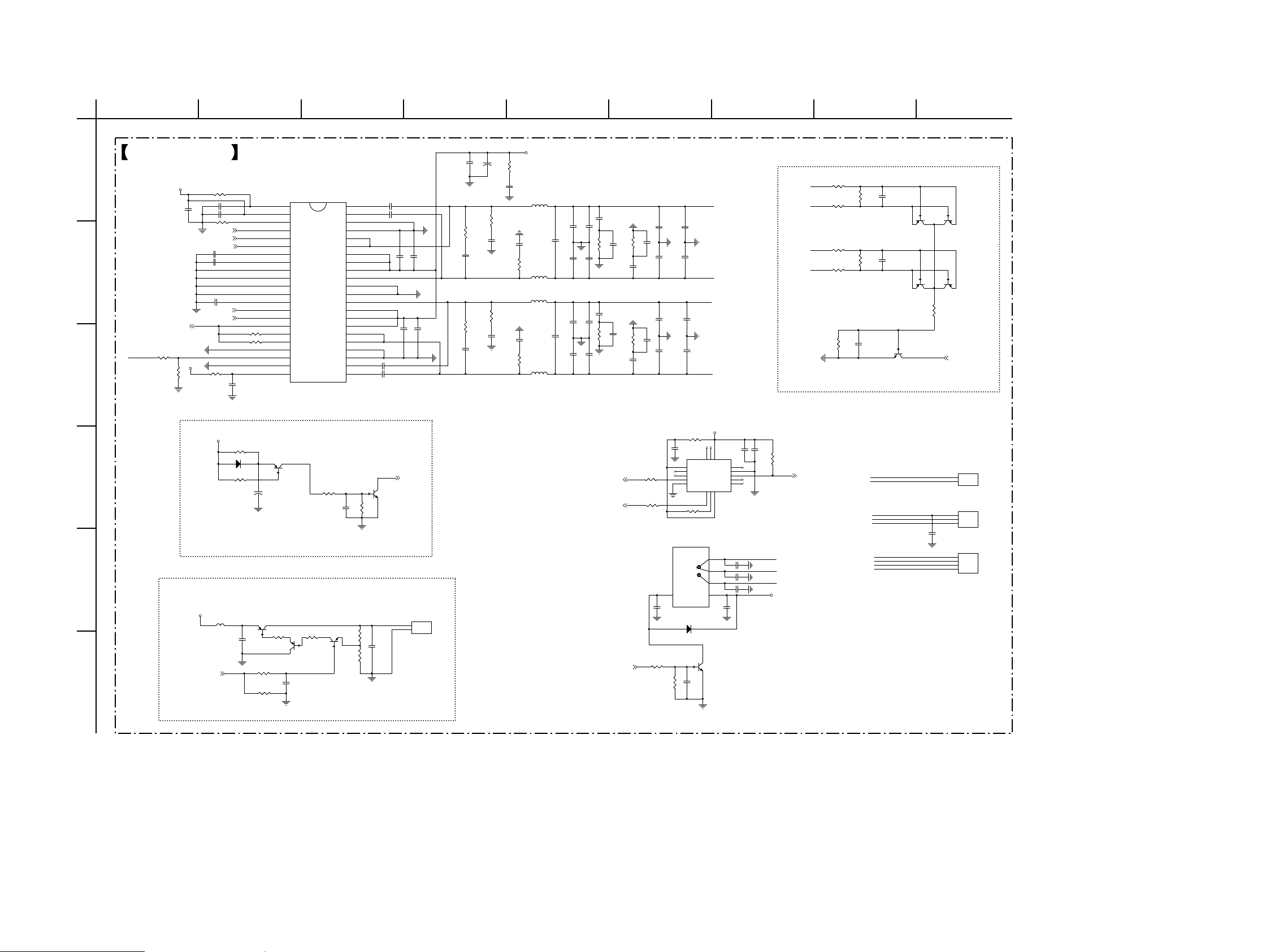
GTK-XB7
4-11. SCHEMATIC DIAGRAM - MAIN Board (8/8) -
2 9
(8/8)MAIN BOARD
A
V_12V
B
C
DVDD_M21
AMP_FAULT5,11
R330 NC/47R330 NC/47
R3310R331
R316 3.3R316 3.3
C264 0.1uFC264 0.1uF
C266
C266
C267
C267
10UF
10UF
V_12V
0
R317 24KR317 24K
11
11
C273
C273
C332 1uFC332 1uF
C333 1uFC333 1uF
R334
R334
OUT2A11
OUT2B
OUT1A11
OUT1B11
0.1uF
0.1uF
VALID
0.1uF
0.1uF
3.3
3.3
R328 NC/0R328 NC/0
R329 NC/0R329 NC/0
C296
C296
0.1uF
0.1uF
DVDD_M21
U18
U18
1
GVDD_AB
2
VDD
3
OC_ADJ
4
/RESET
5
INPUT_A
6
INPUT_B
7
C_START
8
DVDD
9
GND
10
GND
11
GND
12
GND
13
AVDD
14
INPUT_C
15
INPUT_D
16
/FAULT
17
/OTW
18
/CLIP
19
M1
20
M2
21
M3
TAS5624A
TAS5624A
BST_A
BST_B
OUT_A
OUT_A
PVDD_AB
PVDD_AB
PVDD_AB
OUT_B
OUT_C
PVDD_CD
PVDD_CD
PVDD_CD
OUT_D
OUT_D
BST_C
BST_DGVDD_CD
• See page 44 for IC Block Diagrams.
386
++
C263
C263
CE25
CE25
R333
820uF/50V
820uF/50V
R366
R366
5.6
5.6
C317
C317
270pF/50V/X7R
270pF/50V/X7R
R367
R367
5.6
5.6
C320
C320
270pF/50V/X7R
270pF/50V/X7R
R333
5.6
5.6
C316
C316
330pF/50V
330pF/50V
0.1uF
0.1uF
44
C265 0.033uF/50V/X7RC265 0.033uF/50V/X7R
43
C268 0.033uF/50V/X7RC268 0.033uF/50V/X7R
42
GND
41
GND
40
39
38
37
36
35
34
GND
33
GND
32
31
30
29
28
27
26
GND
25
GND
24
2322
C274
C274
1000pF/50V/X7R
1000pF/50V/X7R
C288
C288
C295
C295
0.033uF/50V/X7R
0.033uF/50V/X7R
C297 0.033uF/50V/X7RC297 0.033uF/50V/X7R
C280
C280
0.1uF
0.1uF
C286
C286
1000pF/50V/X7R
1000pF/50V/X7R
0.1uF
0.1uF
R319
R319
NC/5.6
NC/5.6
C298
C298
NC/100pF/50V/NP0
NC/100pF/50V/NP0
R326
R326
NC/5.6
NC/5.6
C299
C299
NC/100pF/50V/NP0
NC/100pF/50V/NP0
AMP_36V
L485
L485
10uH/12A
10uH/12A
C322
C322
270pF/50V/X7R
270pF/50V/X7R
R368
R368
5.6
5.6
L486
L486
10uH/12A
10uH/12A
L487
L487
10uH/12A
10uH/12A
C329
C329
270pF/50V/X7R
270pF/50V/X7R
R372
R372
5.6
5.6
L488
L488
10uH/12A
10uH/12A
5
C271
C271
0.01uF/50V/X7R
C1750
C1750
1ȝF
1ȝF
C272
C272
C1751
C1751
1ȝF
1ȝF
C1752
C1752
1ȝF
1ȝF
C289
C289
C1753
C1753
1ȝF
1ȝF
0.01uF/50V/X7R
C1754
C1754
1ȝF
1ȝF
C275
C275
R320
R320
1uF/63V
1uF/63V
C1755
C1755
C1757
C1757
1uF/63V
1uF/63V
C1756
C1756
NC/0.01uF/50V/X7R
NC/0.01uF/50V/X7R
3.3
3.3
1ȝF
1ȝF
C335
C335
0.01uF/50V/X7R
0.01uF/50V/X7R
ȝF
1ȝF
1
C287
C287
R327
R327
NC/0.01uF/50V/X7R
NC/0.01uF/50V/X7R
3.3
3.3
1ȝF
1ȝF
714
L+
R773 220KR773 220K
L+
C269
C269
C270
C270
0.1uF
0.1uF
1000pF/50V/X7R
1000pF/50V/X7R
C276
C276
R318
R318
NC/0.01uF/50V/X7R
NC/0.01uF/50V/X7R
3.3
3.3
C281
C281
C283
C283
0.1uF
0.1uF
1000pF/50V/X7R
1000pF/50V/X7R
C279
C279
0.01uF/50V/X7R
0.01uF/50V/X7R
C285
C285
1000pF/50V/X7R
1000pF/50V/X7R
C290
C290
R325
R325
NC/0.01uF/50V/X7R
NC/0.01uF/50V/X7R
3.3
3.3
C291
C291
1000pF/50V/X7R
1000pF/50V/X7R
C334
C334
0.01uF/50V/X7R
0.01uF/50V/X7R
L-
R+
C292
C292
0.1uF
0.1uF
C293
C293
0.1uF
0.1uF
R-
L-
R774 220KR774 220K
R+
R776 220KR776 220K
R-
R777 220KR777 220K
R775
R775
C530
C530
220K
220K
10uF
10uF
Q756
Q756
Q757
PNP_3CG3906M
PNP_3CG3906M
R778
R778
C531
C531
220K
220K
10uF
10uF
PNP_3CG3906M
PNP_3CG3906M
C769
C769
R783
R783
100K
100K
0.22uF
0.22uF
Q21
Q21
NPN_3DG3904M
NPN_3DG3904M
Q757
PNP_3CG3906M
PNP_3CG3906M
Q758
Q758
Q759
Q759
PNP_3CG3906M
PNP_3CG3906M
R782
R782
100
100
AMP_FAULT
DC detect
D
36V_MAIN
R321 NC/100KR321 NC/100K
D8
R323 NC/10KR323 NC/10K
NC/LL4148D8NC/LL4148
Q19
Q19
NC/PNP_3CG9012M
NC/PNP_3CG9012M
++
CE6
CE6
NC/100uF/50V
NC/100uF/50V
R322 NC/10KR322 NC/10K
C282
C282
NC/0.1UF
NC/0.1UF
R324
R324
NC/10K
NC/10K
VALID 11,12
Q20
Q20
NC/NPN_3DG3904M
NC/NPN_3DG3904M
R232 100R232 100
I2C_SCL5
R265 100R265 100
I2C_SDA
5
Power OFF Mute Circuit
E
5
FAN CONTROL
V_12V
500/800mA
500/800mA
FB25
FB25
FAN_PWM
F
C302
C302
4.7uF
4.7uF
Q253
Q253
PNP_MMBT8550C
PNP_MMBT8550C
R298 4.7KR298 4.7K
PNP_3CG3906M
PNP_3CG3906M
R358 10KR358 10K
R357 100KR357 100K
R355
Q255
Q255
NPN_3DG3904M
NPN_3DG3904M
C300
C300
1UF/16V/X7R
1UF/16V/X7R
4.7K
4.7K
Q254
Q254
Vb
C301
C301
Vfb
R359
R359
1.2K
1.2K
R356
R356
100K
100K
R355
VCC_FAN
4.7uF
4.7uF
1
2
XP14
XP14
1
2
2PIN/2.0mm
2PIN/2.0mm
Relay_EN
C773
C773
0.01uF/50V/X7R
0.01uF/50V/X7R
R77 10KR77 10K
5
R60
R60
47K
47K
R362 0R362 0
C188
C188
0.1UF
0.1UF
16
U35
U35
1
NC5
VDD_IO
2
NC1
3
NC2
4
SCL
5
GND1
SDA
6
KXCJK-1013
KXCJK-1013
R363 10KR363 10K
SW6
SW6
4
1
3
2
G5LE-1
G5LE-1
D7 MBRX180/80V/1AD7 MBRX180/80V/1A
Q6
Q6
NPN_3DG3904M
NPN_3DG3904M
C323
C323
0.1UF
0.1UF
3.3V_D1
15
14
NC4
ADDR
7
8
4
1
3
2
VDD
RES1
GND2
RES3
RES2
NC3
INT
C50
C50
C161
C161
10uF/6.3V/X5R
10uF/6.3V/X5R
13
12
11
10
9
G-Sensor
C770 1000pF/50V/X7RC770 1000pF/50V/X7R
C771 1000pF/50V/X7RC771 1000pF/50V/X7R
C772 1000pF/50V/X7RC772 1000pF/50V/X7R
C774
C774
0.01uF/50V/X7R
0.01uF/50V/X7R
0.1UF
0.1UF
R136
R136
4.7K
4.7K
G_INT
S1
R-
S2
V_12V
L+
L-
RW+
R+
R-
S2
RW+
S1
RW+
1
2
1
2
3
C775
C775
NC/0.01uF/50V/X7R
NC/0.01uF/50V/X7R
1
2
3
4
XP21
XP21
1
L 3
2
2PIN_3.96mm
2PIN_3.96mm
XP22
XP22
RW 6
1
2
R 3
3
3PIN_3.96mm
3PIN_3.96mm
XP10
XP10
1
2
3
4
4PIN/2.5mm
4PIN/2.5mm
GTK-XB7
3333
Page 34
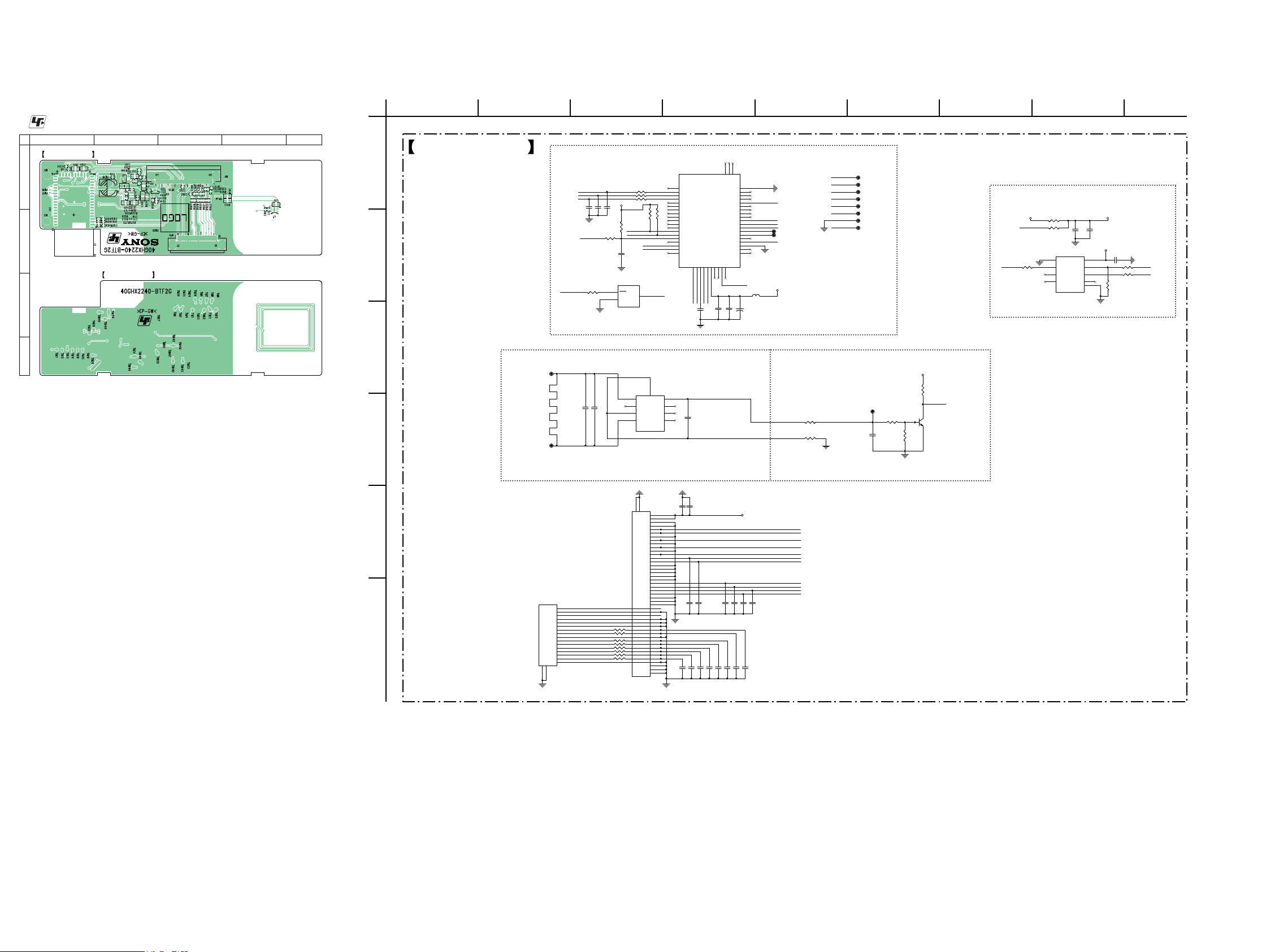
GTK-XB7
4-12. PRINTED WIRING BOARD - BT&NFC Board -
• See page 24 for Circuit Boards Location.
• : Uses unleaded solder.
1 2 3 4 5
BT&NFC BOARD (COMPONENT SIDE)
A
B
BT&NFC BOARD (CONDUCTOR SIDE)
C
D
4-13. SCHEMATIC DIAGRAM - BT&NFC Board -
2 9
386
BT&NFC BOARD
C108
C108
NC/15pF/50V/NP0
NC/15pF/50V/NP0
C110
C110
C107
C107
NC/15pF/50V/NP0
NC/15pF/50V/NP0
NC/15pF/50V/NP0
NC/15pF/50V/NP0
R270
R270
NC/100K
NC/100K
R273 1KR273 1K
BT
BT_3.3V
A
BT_LRCK1
BT_BCLK1
BT_DATA1
BT_RESET1
B
BT_RESET1
2
0
R3680R368
1
C
TP63TP63
C18
C18
C2
120pF/50V/NP0C2120pF/50V/NP0
20pF/50V/NP0
PCB LAYOUT ANTENNA
D
TP62TP62
20pF/50V/NP0
BUILT-IN BLUETOOTH MODULE ANTENNA SECTION
U12
R103 33R103 33
R108 33R108 33
R110 33R110 33
CP_SCL
CP_SDA
C124
C124
NC/0.1uF/25V/X5R
NC/0.1uF/25V/X5R
U26
U26
RST
VCC
GND
SGM803
SGM803
P24
NFC_BT1
3
R225
R225
2.2K
2.2K
BAT_IN
U12
BT_BM63
BT_BM63
1
DR0
2
RFS0
3
SCLK0
4
DT0
5
AOHPR
6
AOHPM
7
AOHPL
8
R226
R226
MICN1
9
MICP1
10
MICBIAS
11
AIR
12
NC/2.2K
NC/2.2K
AIL
13
P12
14
P13
15
RST_N
16
P01
17
P24
18
P04
19
P15
HCI_RXD
HCI_TXD
CODEC_VO
VDD_IO
ADAP_IN
BAT_IN
202122232425262728
ADAP_IN
BT_TX1
BT_RX1
BT_VDDIO
C105
C105
NC/10UF/6.3V/X5R
NC/10UF/6.3V/X5R
AMB_DET
SYS_PWR
BAT_IN
C104
C104
100pF/50V/NP0
100pF/50V/NP0
515049
PWR
29
ANT3
ANT2
ANT1
48
GND
47
P05
46
P30
45
P27
44
P20
43
P02
42
P31
41
P33
40
P36
39
DP
38
DM
37
EAN
36
P03
35
P00
34
P35
33
P37
32
GND
31
LED1
30
LED2
LED3
MFB1
L3 120/2AL3 120/2A
CE18
CE18
C115
C115
++
0.1UF
0.1UF
220uF/16V
220uF/16V
NFC
9
U7
VDDA
VB
GND
NC
VSS
VA NIRQ
MN63Y1212U7MN63Y1212
8
7
NC
6
NC
C69
C69
1uF
1uF
1
2
3
45
BM_D+_1
BM_D-_1
CP_Reset
EAN
P20
BT_3.3V
5
P20
TM11TM11
BAT_IN
TM12TM12
EAN
TM13TM13
ADAP_IN
TM14TM14
BT_RX1
TM16TM16
BT_TX1
TM15TM15
TM19TM19
P24
TM17TM17
TM18TM18
R1410R141
0
R1430R143
0
TM20TM20
BT_3.3V
R106
R106
100K
100K
TP56TP56
NFC
R105 100KR105 100K
C290
C290
100pF/50V/NP0
100pF/50V/NP0
NFC_INT1
Q9
Q9
NPN_3DG3904M
NPN_3DG3904M
R2291MR229
1M
714
Apple Authentication
Active Mode Current : 7.5mA
CP_SDA
BT_3.3V
BT_VDDIO
R220 33R220 33
R109
R109
R1110R111
NC/0
NC/0
0
U15U15
1
GND
2
SDA
3
NC
45
NC NC
AUTHENTICATION IC 2.0C
CP3V3
C116
C116
C106
C106
0.1UF
0.1UF
10uF
10uF
CP3V3
C111
C111
0.1UF
0.1UF
8
VCC
7
RST
6
SCL
9
GND
CP_Reset
0
R3750R375
R22333R223
CP_SCL
33
R378
R378
NC/0
NC/0
NFC CIRCUIT REFERENCE 40GKB630U-NFC2G
C336
C336
C337
C337
10uF
10uF
0.1UF
46
47
45
XP34
XP34
45PIN/0.5mm
45PIN/0.5mm
45
44
44
GND
GND
43
43
42
42
41
41
40
40
39
39
38
38
37
37
36
36
35
35
34
34
33
33
32
32
31
31
30
30
29
29
28
28
27
27
26
26
25
25
24
24
23
23
22
22
21
21
20
20
19
19
18
18
17
17
16
16
15
15
14
14
13
13
12
12
11
11
10
10
9
9
8
8
7
7
6
6
5
5
4
4
3
3
2
2
1
1
To Main Board
E
To Key Board
1
1
2
2
3
3
4
4
5
5
6
6
7
7
8
XP8
XP8
8
16pin/1.0
F
16pin/1.0
9
9
10
10
11
11
12
12
13
13
14
14
15
15
16
16
GND
GND
17
18
R917 0R917 0
R918 0R918 0
R919 0R919 0
R920 0R920 0
R921 0R921 0
R922 0R922 0
R923 0R923 0
R924 0R924 0
0.1UF
C338
C353
C353
C338
NC/15pF/50V/NP0
NC/15pF/50V/NP0
NC/15pF/50V/NP0
NC/15pF/50V/NP0
C357
C358
C356
C357
C355
C358
C356
C355
15pF/50V/NP0
15pF/50V/NP0
15pF/50V/NP0
15pF/50V/NP0
15pF/50V/NP0
15pF/50V/NP0
BT_3.3V
BM_D-_1
BM_D+_1
BT_LRCK1
BT_BCLK1
BT_DATA1
NFC_BT1
BT_RESET1
BT_RX1
BT_TX1
MFB1
C350
C351
C354
C351
C352
C352
C354
C350
NC/15pF/50V/NP0
NC/15pF/50V/NP0
NC/15pF/50V/NP0
NC/15pF/50V/NP0
NC/15pF/50V/NP0
NC/15pF/50V/NP0
C359
C361
C361
C359
C360
C360
C362
C362
15pF/50V/NP0
15pF/50V/NP0
15pF/50V/NP0
15pF/50V/NP0
15pF/50V/NP0
15pF/50V/NP0
15pF/50V/NP0
15pF/50V/NP0
15pF/50V/NP0
15pF/50V/NP0
NFC_INT1
NC/15pF/50V/NP0
NC/15pF/50V/NP0
GTK-XB7
3434
Page 35
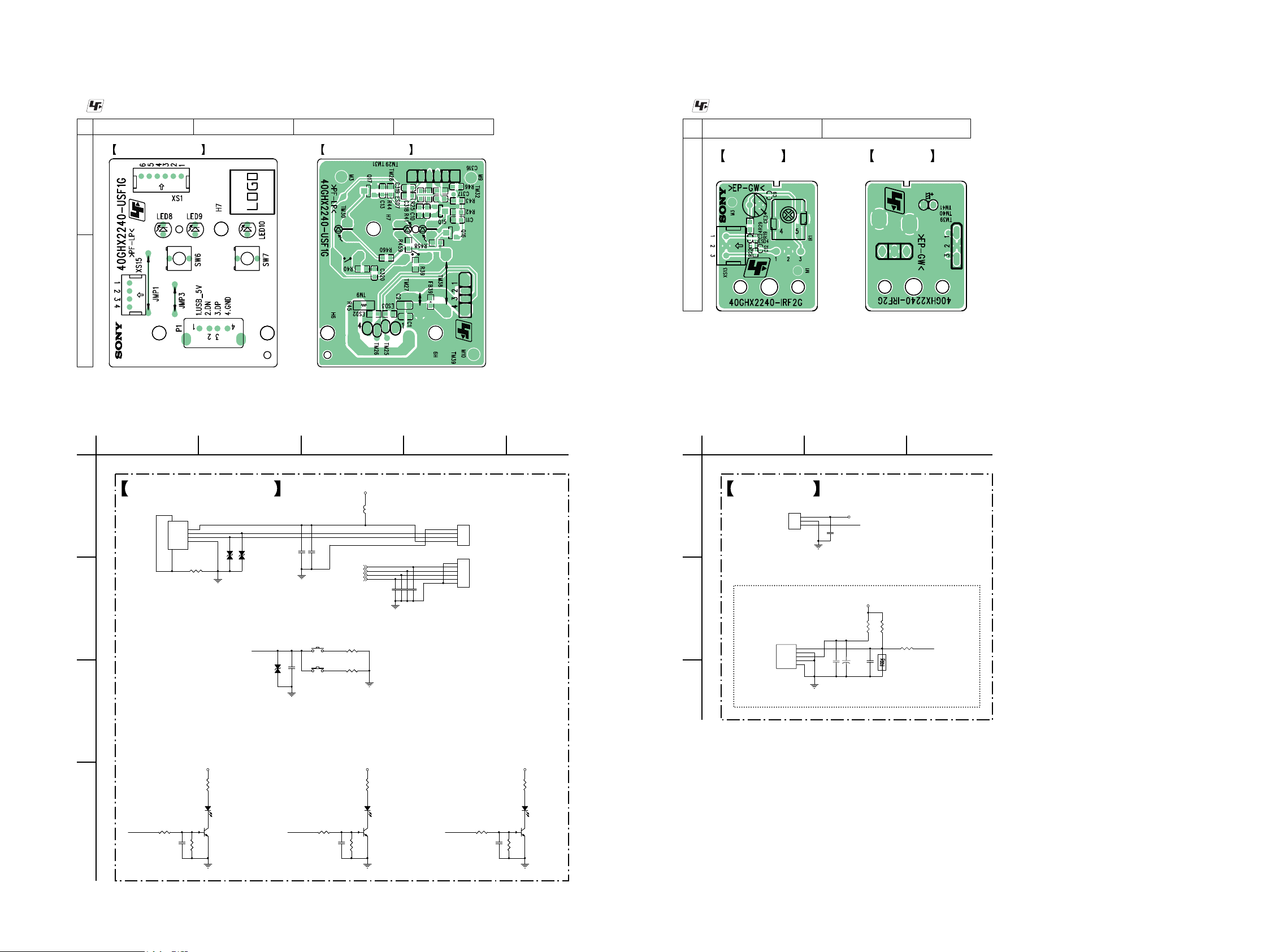
GTK-XB7
4-14. PRINTED WIRING BOARD - USB + KEY Board -
• : Uses unleaded solder.
1 2 3 4
USB + KEY BOARD (COMPONENT SIDE) USB + KEY BOARD (CONDUCTOR SIDE)
A
B
• See page 24 for Circuit Boards Location.
4-16. PRINTED WIRING BOARD - IR Board -
• : Uses unleaded solder.
1 2
IR BOARD
(COMPONENT SIDE)
IR BOARD
(CONDUCTOR SIDE)
A
• See page 24 for Circuit Boards Location.
4-15. SCHEMATIC DIAGRAM - USB + KEY Board -
14
USB + KEY BOARD
A
USB
65
P1
1
VCC
2
Shell BShell A
GND
DN
D-
3
DP
D+
4
4Pin/2mmP1 4Pin/2mm
R450R45
ESD2
ESD3
ESD2
ESD3
EGA10603V05A1-B
EGA10603V05A1-B
EGA10603V05A1-B
EGA10603V05A1-B
0
C2
C1
0.1uFC10.1uF
10uFC2 10uF
B
SW6SW6
2.2V
ADC_KEY1
ESD7
ESD7
NC/EGA10603V05A1-B
NC/EGA10603V05A1-B
C320 47pF/50V/NP0C320 47pF/50V/NP0
ADD SPKADD SPK
SW7SW7
PARTY CHAINPARTY CHAIN
R39 20KR39 20K
2.72V
R40 47KR40 47K
C
32
ADC_KEY1
Blue_LED5
Blue_LED6
Blue_LED7
USB_5V
FB39
FB39
500/800mA
500/800mA
4-17. SCHEMATIC DIAGRAM - IR Board -
5
1
32
IR BOARD
A
XS15
XS15
1
1
2
2
3
3
4
4
4PIN/2.0mm/200mm
4PIN/2.0mm/200mm
XS1
XS1
1
1
2
2
3
3
4
4
C318 47pF/50V/NP0C318 47pF/50V/NP0
C319 47pF/50V/NP0C319 47pF/50V/NP0
C316 47pF/50V/NP0C316 47pF/50V/NP0
C317 47pF/50V/NP0C317 47pF/50V/NP0
5
5
6
6
6PIN/2.0mm/120mm
6PIN/2.0mm/120mm
B
XS13
XS13
1
2
3
3PIN/2.0mm/180mm
3PIN/2.0mm/180mm
IR
IR1
IR1
IR
GND
VCC
GND
GND
IRR_5P
IRR_5P
1
2
3
1
2
3
4
5
C24
C24
0.1UF
0.1UF
STB_5V_1
IR_1
STB_5V_1
R19
R19
R29
R29
4.7K
4.7K
100
100
IR_1
R22 1KR22 1K
ESD4
ESD4
NC/LVSL10180Z020/18V/2pF
NC/LVSL10180Z020/18V/2pF
C12
C12
C9
++
CE3
CE3
NC/47pF/50V/NP0
47uF/10V
47uF/10V
NC/47pF/50V/NP0
21
0.1UFC90.1UF
C
GTK-XB7
D
USB_5V USB_5V USB_5V
R458
R458
220
220
LED8
LED8
L
LED_GREEN
LED_GREEN
Blue_LED5 Blue_LED6 Blue_LED7
R25 4.7KR25 4.7K
Q15
Q15
NPN_3DG3904M
NPN_3DG3904M
C10
C10
R41
R41
0.1uF
0.1uF
10K
10K
R43 4.7KR43 4.7K
R459
R459
220
220
LED9
LED9
LED_GREEN
LED_GREEN
Q16
Q16
NPN_3DG3904M
NPN_3DG3904M
C11
C11
R42
R42
0.1uF
0.1uF
10K
10K
R46 4.7KR46 4.7K
R460
R460
220
220
LED10
LED10
strap dloMR
LED_GREEN
LED_GREEN
Q17
Q17
NPN_3DG3904M
NPN_3DG3904M
C13
C13
R44
R44
0.1uF
0.1uF
10K
10K
3535
Page 36

GTK-XB7
4-18. PRINTED WIRING BOARD - CONTROL Board -
1 2 3 4 5 6 7 8 9 10
CONTROL BOARD (COMPONENT SIDE)
A
B
C
• See page 24 for Circuit Boards Location.
• : Uses unleaded solder.
CONTROL BOARD (CONDUCTOR SIDE)
D
E
F
GTK-XB7
3636
Page 37

4-19. SCHEMATIC DIAGRAM - CONTROL Board -
GTK-XB7
D
A
B
C
2 9
CONTROL BOARD
To Main Board
XP16
XP16
1
2
3
4
5
6
7
8
9
10
11
12
13
14
15
16
16PIN/1.0mm
16PIN/1.0mm
STB_5V
R457
R457
R456
R456
220
220
220
220
PW_LED1 PW_LED2
R28 4.7KR28 4.7K
POWER
Q13
Q13
Q14
Q14
NPN_3DG3904M
NPN_3DG3904M
NPN_3DG3904M
C7
0.1uFC70.1uF
NPN_3DG3904M
C8
R32
R30
R30
10K
10K
R32
10K
10K
123
LED1
LED1
PIN-1 GREEN
PIN-3 RED
LED_3P_2PARTA
LED_3P_2PARTA
0.1uFC80.1uF
1
2
3
4
5
6
7
8
9
10
11
12
13
14
15
16
R31 4.7KR31 4.7K
386
C306
C306
C307
C307
0.1uF
0.1uF
0.1uF
0.1uF
C308 47pF/50V/NP0C308 47pF/50V/NP0
C309 47pF/50V/NP0C309 47pF/50V/NP0
C310 47pF/50V/NP0C310 47pF/50V/NP0
FB40 500/800mAFB40 500/800mA
R8150R815
R8160R816
R8090R809
R8100R810
R8110R811
R8120R812
R8130R813
R8140R814
C314 47pF/50V/NP0C314 47pF/50V/NP0
C315 47pF/50V/NP0C315 47pF/50V/NP0
C312 47pF/50V/NP0C312 47pF/50V/NP0
C311 47pF/50V/NP0C311 47pF/50V/NP0
C313 47pF/50V/NP0C313 47pF/50V/NP0
LED
Blue_LED1 Blue_LED2 Blue_LED3 Blue_LED4
POWER_KEY
0
0
0
0
0
0
0
0
R19 4.7KR19 4.7K
STB_5V
ADC_KEY
Blue_LED1
Blue_LED2
Blue_LED3
Blue_LED4
PW_LED1
PW_LED2
STB_5V STB_5V STB_5V STB_5V
R452
R452
470
470
LED4
LED4
BT USB
C3
R35
R35
0.1uFC30.1uF
10K
10K
Q9
Q9
NPN_3DG3904M
NPN_3DG3904M
LED_BULE
LED_BULE
5
R21 4.7KR21 4.7K
ESD6
ESD6
NC/EGA10603V05A1-B
NC/EGA10603V05A1-B
C4
R34
R34
0.1uFC40.1uF
10K
10K
C22
C22
47pF/50V/NP0
47pF/50V/NP0
R4531KR453
1K
LED5
LED5
LED_WHITE
LED_WHITE
Q10
Q10
NPN_3DG3904M
NPN_3DG3904M
SW3SW3
Mega BassMega Bass
SW2SW2
VOL+VOL+
SW1SW1
VOL-VOL-
0V
R38 100R38 100
1.0V
R23 4.7KR23 4.7K
1.65V
R36 10KR36 10K
KEY
R24 4.7KR24 4.7K
POWER_KEYADC_KEY
AUX
C5
0.1uFC50.1uF
R33
R33
10K
10K
714
ESD5
ESD5
C21
C21
NC/EGA10603V05A1-B
NC/EGA10603V05A1-B
R4541KR454
1K
LED6
LED6
LED_WHITE
LED_WHITE
Q11
Q11
NPN_3DG3904M
NPN_3DG3904M
SW5SW5
0V
R37 100R37 100
PowerPower
47pF/50V/NP0
47pF/50V/NP0
SW4SW4
FunctionFunction
1.0V
R20 4.7KR20 4.7K
MEGA BASS
R26 4.7KR26 4.7K
R455
R455
220
220
LED7
LED7
LED_RED
LED_RED
Q12
Q12
NPN_3DG3904M
NPN_3DG3904M
C6
R27
R27
0.1uFC60.1uF
10K
10K
E
STB_5V STB_5V
R1 0R1 0
R2 0R2 0
R3 0R3 0
GTK-XB7
3737
Page 38
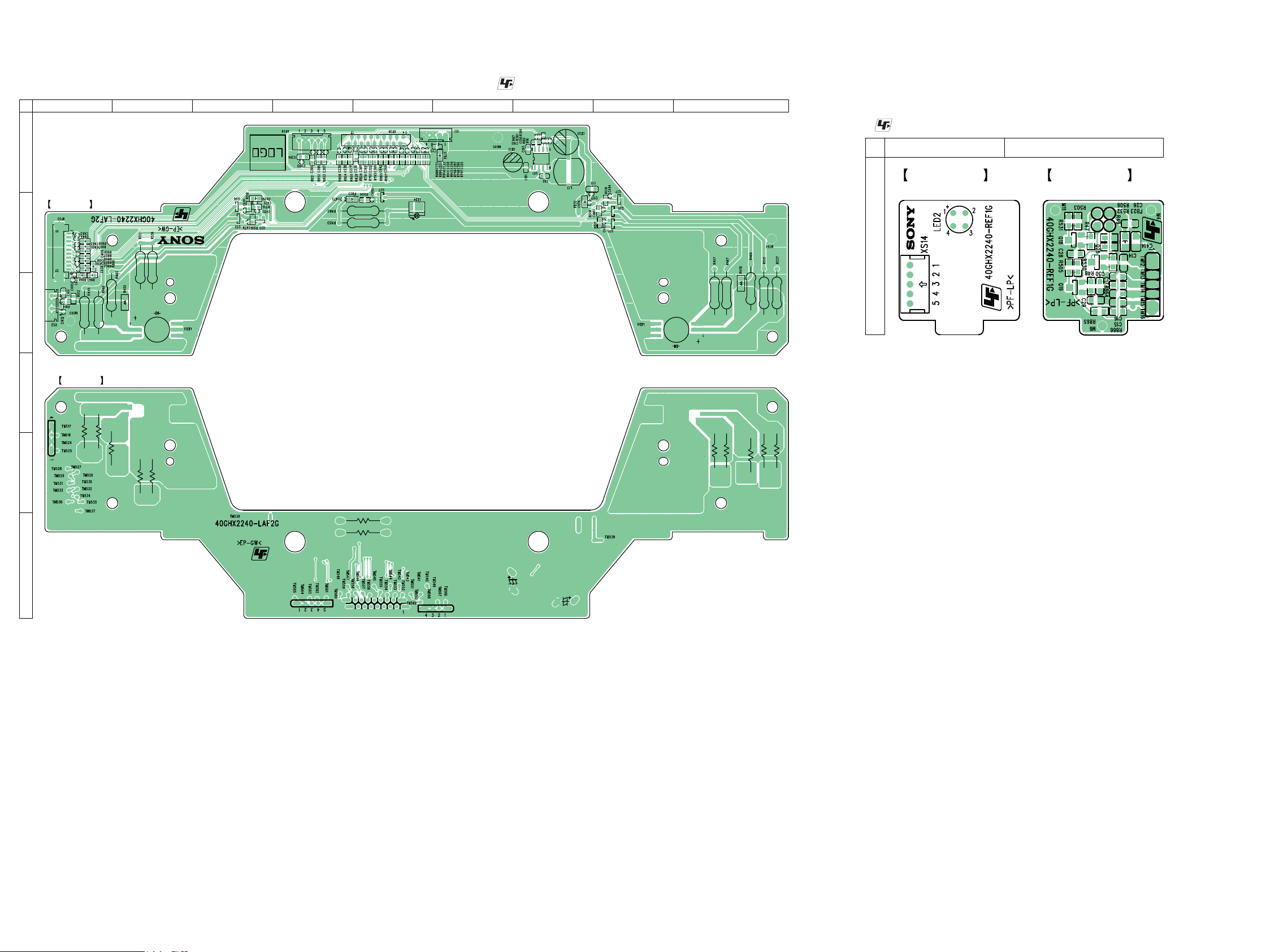
GTK-XB7
4-20. PRINTED WIRING BOARD - LA Board -
1 2 3 4 5 6 7 8 9
A
LA BOARD (COMPONENT SIDE)
B
C
LA BOARD (CONDUCTOR SIDE)
D
• See page 24 for Circuit Boards Location.
• : Uses unleaded solder.
4-21. PRINTED WIRING BOARD - RGBE Board -
• See page 24 for Circuit Boards Location.
• : Uses unleaded solder.
1 2
RGBE BOARD
(COMPONENT SIDE)
RGBE BOARD
(CONDUCTOR SIDE)
A
E
F
GTK-XB7
3838
Page 39

GTK-XB7
4-22. SCHEMATIC DIAGRAM - LA Board -
2 9
LA BOARD
A
To Mainboard
XS1
XS1
1
1
2
2
3
3
4
4
4PIN/2.0mm/160mm
4PIN/2.0mm/160mm
To Mainboard
XP38
XP38
18
18
17
17
16
16
15
15
14
14
18PIN/1.0mm
18PIN/1.0mm
13
13
12
12
11
11
10
10
9
9
8
8
7
7
6
6
5
5
4
4
3
3
2
2
1
1
C259 100pF/50V/NP0C259 100pF/50V/NP0
C258 100pF/50V/NP0C258 100pF/50V/NP0
B
+12V_1
C20
C20
0.1uF/50V/X7R
0.1uF/50V/X7R
R804 0R804 0
R805 0R805 0
R806 0R806 0
R828 0R828 0
R829 0R829 0
R791 0R791 0
R792 0R792 0
R793 0R793 0
R797 0R797 0
R798 0R798 0
R799 0R799 0
R885 0R885 0
R897 0R897 0
R898 0R898 0
R899 0R899 0
R900 0R900 0
R901 0R901 0
C367 100pF/50V/NP0C367 100pF/50V/NP0
C239 100pF/50V/NP0C239 100pF/50V/NP0
C250 100pF/50V/NP0C250 100pF/50V/NP0
C251 100pF/50V/NP0C251 100pF/50V/NP0
C252 100pF/50V/NP0C252 100pF/50V/NP0
C366 100pF/50V/NP0C366 100pF/50V/NP0
C236 100pF/50V/NP0C236 100pF/50V/NP0
C237 100pF/50V/NP0C237 100pF/50V/NP0
C238 100pF/50V/NP0C238 100pF/50V/NP0
C249 100pF/50V/NP0C249 100pF/50V/NP0
R902 0R902 0
C322 100pF/50V/NP0C322 100pF/50V/NP0
C260 100pF/50V/NP0C260 100pF/50V/NP0
C320 100pF/50V/NP0C320 100pF/50V/NP0
C287 100pF/50V/NP0C287 100pF/50V/NP0
C442 100pF/50V/NP0C442 100pF/50V/NP0
C346 100pF/50V/NP0C346 100pF/50V/NP0
C
C92 0.01uF/50V/X7RC92 0.01uF/50V/X7R
U21
U21
AS5430A
+12V_1
FB33 120/2AFB33 120/2A
CE13
CE13
C191
C191
D
++
100uF/16V
100uF/16V
LED_PW_EN_1
0.1uF
0.1uF
R871KR87
R381
R381
47K
47K
1K
AS5430A
3
L13 10uH/3AL13 10uH/3A
1
BS
2
IN
C192
C192
0.1uF
0.1uF
SW
5
FB
67
COMPEN
GND
SS
TP
4
8
9
C193
C193
0.1uF
0.1uF
C156
C156
3900pF/50V/X7R
3900pF/50V/X7R
R384
R384
6.8K
6.8K
VOUT=0.925*(47+13)/13=4.27V
E
To LED B
XS2
XS2
1
1
2
2
3
3
4
4
4PIN/2.0mm/160mm
4PIN/2.0mm/160mm
To LED B
XP55
XP55
10PIN/1.25mm
10PIN/1.25mm
1
2
3
4
5
6
7
8
9
10
GND
F
GND
11
12
C411
C411
0.1uF/50V/X7R
0.1uF/50V/X7R
1
2
3
4
5
6
7
8
9
10
C443 100pF/50V/NP0C443 100pF/50V/NP0
C412
C412
100pF/50V/NP0
100pF/50V/NP0
C444 100pF/50V/NP0C444 100pF/50V/NP0
C445 100pF/50V/NP0C445 100pF/50V/NP0
R913 0R913 0
R914 0R914 0
C406 100pF/50V/NP0C406 100pF/50V/NP0
C405 100pF/50V/NP0C405 100pF/50V/NP0
C408 100pF/50V/NP0C408 100pF/50V/NP0
C407 100pF/50V/NP0C407 100pF/50V/NP0
C409 100pF/50V/NP0C409 100pF/50V/NP0
C410 100pF/50V/NP0C410 100pF/50V/NP0
386
UPPER RIGHT CORNER RGB A UPPER LEFT CORNER RGB B UPPER CENTER FLASH LED A
5V_D2_1
PWM1_B_1
C479
C479
0.1UF
0.1UF
PWM1_G_1
C480
C480
0.1UF
0.1UF
R516
R516
4.7K
4.7K
PWM1_R_1
C481
C481
0.1UF
0.1UF
R512
R512
NC/22ohm
NC/22ohm
0
To RGB E
XP54
XP54
1
1
2
2
3
3
4
4
5
5
5PIN/2.0mm
5PIN/2.0mm
Flash_LED3_1
Flash_LED4_1
LED_PW_EN_1
5V_D2_1
5V_D2_1
R908 500/200mAR908 500/200mA
R907 500/200mAR907 500/200mA
R906 500/200mAR906 500/200mA
R857 500/200mAR857 500/200mA
R859 500/200mAR859 500/200mA
R858 500/200mAR858 500/200mA
R860 500/200mAR860 500/200mA
R862 500/200mAR862 500/200mA
R861 500/200mAR861 500/200mA
R863 500/200mAR863 500/200mA
C404 100pF/50V/NP0C404 100pF/50V/NP0
PWM5_G_1
PWM5_R_1
PWM5_B_1
PWM1_R_1
PWM1_G_1
PWM1_B_1
PWM2_R_1
PWM2_G_1
PWM2_B_1
PWM3_R_1
PWM3_G_1
PWM3_B_1
PWM4_G_1
PWM4_R_1
PWM4_B_1
CE20
CE20
++
470uF/10V
470uF/10V
R18
R18
47K/1%
47K/1%
R85
R85
13K/1%
13K/1%
Flash_LED4_1
PWM4_B_1
PWM4_R_1
PWM4_G_1
PWM5_B_1
PWM5_R_1
PWM5_G_1
PWM3_B_1
PWM3_G_1
PWM3_R_1
5V_D2_1
C15
C15
C117
C117
0.1uF/16V/X7R
0.1uF/16V/X7R
10uF
10uF
FB29 120/2AFB29 120/2A
R515
R515
4.7K
4.7K
Q34
Q34
PNP_MMBT8550C
PNP_MMBT8550C
R536
R536
R456
R456
22ohm
22ohm
100
100
2
RGBRGB
4
C393
C393
0.1UF
0.1UF
5
R514
R514
4.7K
4.7K
Q33
Q33
PNP_MMBT8550C
PNP_MMBT8550C
R465
R465
R455
R455
22ohm
22ohm
NC/22ohm
NC/22ohm
3
LED3LED3
615
C397 100pF/50V/NP0C397 100pF/50V/NP0
LED_POWER3
C475
C475
0.1UF
0.1UF
Q32
Q32
PNP_MMBT8550C
PNP_MMBT8550C
R466
R466
22ohm
22ohm
C394
C394
10uF
10uF
C395 100pF/50V/NP0C395 100pF/50V/NP0
C396 100pF/50V/NP0C396 100pF/50V/NP0
R851 0R851 0
R852 0R852 0
R853 0R853 0
LED_POWER3
5V_D2_1
PWM5_R_1
PWM5_G_1
PWM5_B_1
PWM2_B_1
PWM2_G_1
PWM2_R_1
4-23. SCHEMATIC DIAGRAM - RGBE Board -
714
1
2
3
RGBE BOARD
A
To CENTER
XS14
XS14
5PIN/2.0mm/40mm
5PIN/2.0mm/40mm
1
1
2
2
3
3
4
4
5
5
C14
C14
C414
C414
0.1uF
0.1uF
10uF
10uF
C16
C17
C15
C15
C16
C17
47pF/50V/NP0
47pF/50V/NP0
47pF/50V/NP0
47pF/50V/NP0
47pF/50V/NP0
47pF/50V/NP0
R864 0R864 0
R865 0R865 0
R866 0R866 0
5V_D2_2
PWM5_R_2
PWM5_G_2
PWM5_B_2
B
FB30 120/2AFB30 120/2A
5V_D2_1
C482
C482
0.1UF
0.1UF
R518
R518
4.7K
4.7K
C483
C483
0.1UF
0.1UF
R519
R519
4.7K
4.7K
C484
C484
0.1UF
0.1UF
R513
R513
R537
R537
NC/22ohm
NC/22ohm
22ohm
22ohm
RGBRGB
0
4
Q36
Q36
PNP_MMBT8550C
PNP_MMBT8550C
Q37
Q37
PNP_MMBT8550C
PNP_MMBT8550C
R468
R468
R458
R458
100
100
2
22ohm
22ohm
3
615
R517
R517
4.7K
4.7K
C476
C476
0.1UF
0.1UF
R457
R457
NC/22ohm
NC/22ohm
LED6LED6
LED_POWER4
Q35
Q35
PNP_MMBT8550C
PNP_MMBT8550C
R467
R467
22ohm
22ohm
LED_POWER4
Flash_LED3_1
R504 470R504 470
FB23 120/2AFB23 120/2A
C485
C485
0.1UF
0.1UF
LED_POWER1
R463
R463
NC/22ohm
NC/22ohm
LED_POWER15V_D2_1
C473
C473
0.1UF
0.1UF
R453
R453
22ohm
22ohm
LED4
LED4
LED_White_2835
LED_White_2835
Q27
Q27
S8050M-C
S8050M-C
FB23 120/2AFB23 120/2A
LED_POWER15V_D2_2
C26
C26
0.1uF
0.1uF
C
LED_POWER1
LED2LED2
4132
GREEN BLUE RED
R47
R47
4.7K
C28
C28
0.1uF
0.1uF
PWM5_R_2
4.7K
Q18
Q18
PNP_3CG3906M
PNP_3CG3906M
R531
R503
R503
R531
NC/100
NC/100
R48
R48
100
100
4.7K
4.7K
Q19
Q19
PNP_3CG3906M
C29
C29
0.1uF
0.1uF
PNP_3CG3906M
R505
R505
R530
R530
NC/200
NC/200
R49
R49
4.7K
4.7K
200
200
Q26
Q26
PNP_3CG3906M
C30
C30
0.1uF
0.1uF
PNP_3CG3906M
R532
R532
R506
R506
NC/150
NC/150
150
150
D
PWM5_G_2
PWM5_B_2
E
GTK-XB7
3939
Page 40
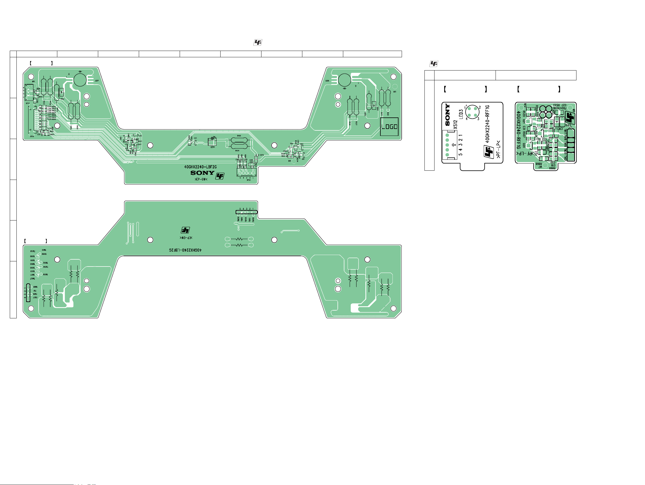
GTK-XB7
4-24. PRINTED WIRING BOARD - LB Board -
1 2 3 4 5 6 7 8 9
LB BOARD (COMPONENT SIDE)
A
B
C
D
• See page 24 for Circuit Boards Location.
• : Uses unleaded solder.
4-25. PRINTED WIRING BOARD - RGBF Board -
• See page 24 for Circuit Boards Location.
• : Uses unleaded solder.
1 2
RGBF BOARD
(COMPONENT SIDE)
RGBF BOARD
(CONDUCTOR SIDE)
A
E
LB BOARD (CONDUCTOR SIDE)
F
GTK-XB7
4040
Page 41
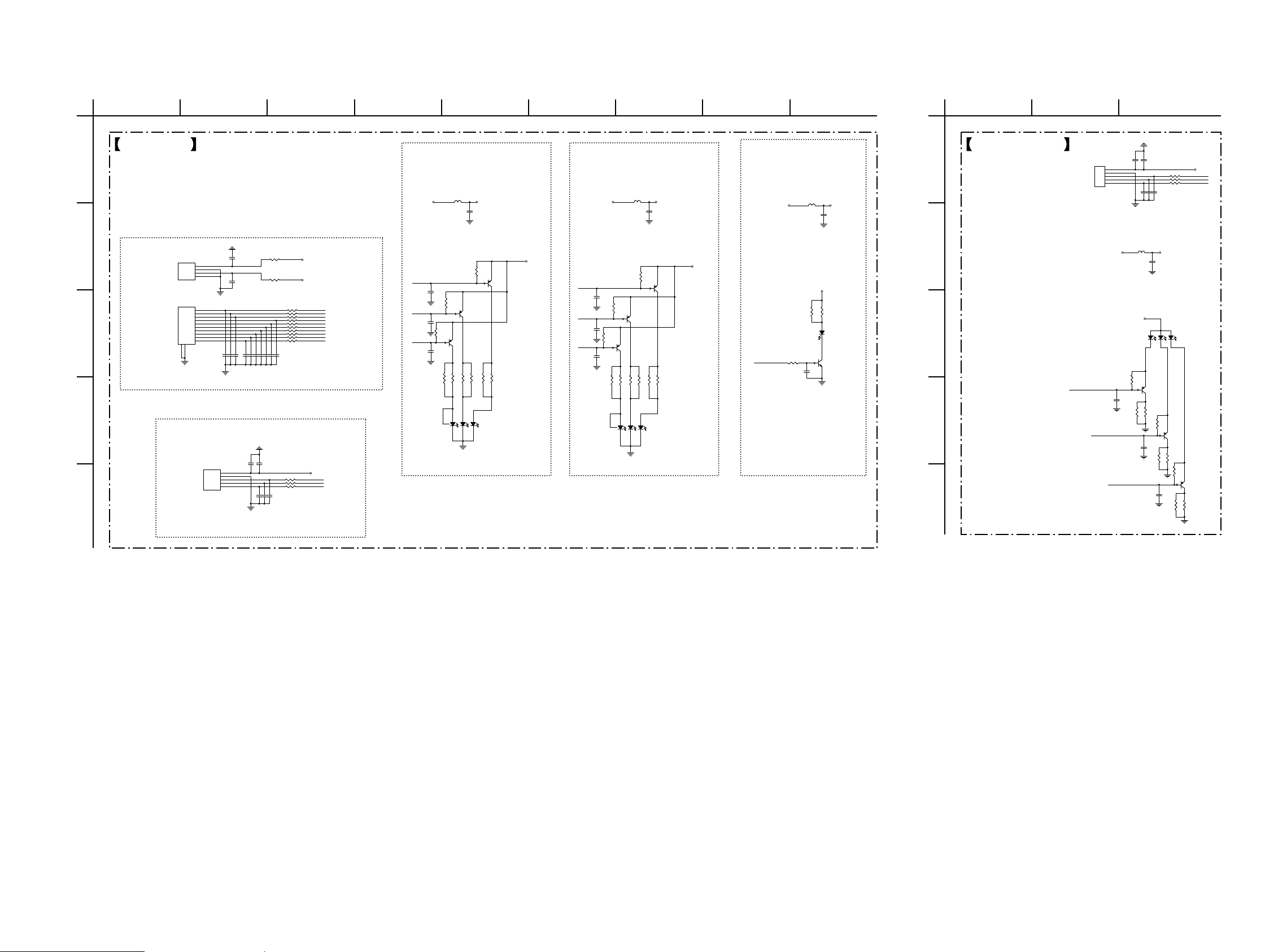
GTK-XB7
4-26. SCHEMATIC DIAGRAM - LB Board -
2 9
LB BOARD
A
B
C
To LEDA
XP37
XP37
4PIN/2.0mm
4PIN/2.0mm
To LED A
XP56
XP56
10PIN/1.25mm
10PIN/1.25mm
GND
GND
11
12
C380
C380
R915 0R915 0
0.1uF/50V/X7R
C370 100pF/50V/NP0C370 100pF/50V/NP0
0.1uF/50V/X7R
C371
C371
100pF/50V/NP0
100pF/50V/NP0
C369 100pF/50V/NP0C369 100pF/50V/NP0
C368 100pF/50V/NP0C368 100pF/50V/NP0
R916 0R916 0
R905 0R905 0
R904 0R904 0
R903 0R903 0
R837 0R837 0
R838 0R838 0
R839 0R839 0
R840 0R840 0
R841 0R841 0
R842 0R842 0
R843 0R843 0
C379 100pF/50V/NP0C379 100pF/50V/NP0
C262 100pF/50V/NP0C262 100pF/50V/NP0
C261 100pF/50V/NP0C261 100pF/50V/NP0
C376 100pF/50V/NP0C376 100pF/50V/NP0
C377 100pF/50V/NP0C377 100pF/50V/NP0
C276 100pF/50V/NP0C276 100pF/50V/NP0
C378 100pF/50V/NP0C378 100pF/50V/NP0
1
1
2
2
3
3
4
4
1
1
2
2
3
3
4
4
5
5
6
6
7
7
8
8
9
9
10
10
D
To RGB F
5PIN/2.0mm
5PIN/2.0mm
C415
C415
C414
0.1UF
0.1UF
XP50
XP50
1
1
2
2
3
3
4
4
5
5
C414
10uF
10uF
R864 0R864 0
R865 0R865 0
R866 0R866 0
C416 100pF/50V/NP0C416 100pF/50V/NP0
C417 100pF/50V/NP0C417 100pF/50V/NP0
C418 100pF/50V/NP0C418 100pF/50V/NP0
E
386
5
LOWER LEFT CORNER RGB D
FB31 120/2AFB31 120/2A
5V_D3_1
5V_D3_1
PWM4_B_2
PWM4_R_2
PWM4_G_2
Flash_LED4_2
PWM5_B_2
PWM5_R_2
PWM5_G_2
PWM3_B_2
PWM3_G_2
PWM3_R_2
PWM5_R_2
PWM5_G_2
PWM5_B_2
5V_D3_1
5V_D3_1
PWM3_B_2
C486
C486
0.1UF
0.1UF
PWM3_G_2
C487
C487
0.1UF
0.1UF
PWM3_R_2
C488
C488
0.1UF
0.1UF
R522
R522
4.7K
4.7K
R523
R523
R521
R521
4.7K
4.7K
Q40
Q40
PNP_MMBT8550C
PNP_MMBT8550C
R538
R538
NC/22ohm
22ohm
NC/22ohm
22ohm
RGBRG B
0
4
C477
C477
0.1UF
0.1UF
Q39
Q39
PNP_MMBT8550C
PNP_MMBT8550C
R470
R460
R460
R470
22ohm
100
100
22ohm
2
3
615
LED_POWER5
R520
R520
4.7K
4.7K
R459
R459
NC/22ohm
NC/22ohm
LED7LED7
Q38
Q38
PNP_MMBT8550C
PNP_MMBT8550C
R469
R469
22ohm
22ohm
LED_POWER5
714
LOWER RIGHT CORNER RGB C LOWER CENTER FLASH LED B
FB32 120/2AFB32 120/2A
LED_POWER65V_D3_1
C478
C478
0.1UF
0.1UF
PWM4_B_2
PWM4_G_2
PWM4_R_2
R524
R524
4.7K
4.7K
C489
C489
0.1UF
0.1UF
R525
R525
4.7K
4.7K
Q42
Q42
PNP_MMBT8550C
R526
R526
4.7K
4.7K
R527
R527
NC/22ohm
NC/22ohm
0
PNP_MMBT8550C
Q43
Q43
PNP_MMBT8550C
PNP_MMBT8550C
R539
R539
R462
R462
R472
R472
22ohm
22ohm
100
100
22ohm
22ohm
2
3
RGBRGB
615
4
R461
R461
R471
R471
NC/22ohm
NC/22ohm
22ohm
22ohm
LED8LED8
C490
C490
0.1UF
0.1UF
C491
C491
0.1UF
0.1UF
Q41
Q41
PNP_MMBT8550C
PNP_MMBT8550C
LED_POWER6
Flash_LED4_2
R510 470R510 470
FB24 120/2AFB24 120/2A
C492
C492
0.1UF
0.1UF
LED_POWER2
R454
R454
R464
R464
22ohm
22ohm
NC/22ohm
NC/22ohm
LED_POWER25V_D3_1
C474
C474
0.1UF
0.1UF
LED5
LED5
LED_White_2835
LED_White_2835
Q31
Q31
S8050M-C
S8050M-C
4-27. SCHEMATIC DIAGRAM - RGBF Board -
1
2
RGBF BOARD
A
To RGB D
XS12
XS12
5PIN/2.0mm/40mm
5PIN/2.0mm/40mm
1
1
2
2
3
3
4
4
5
5
B
C415
C415
10uF
10uF
FB24 120/2AFB24 120/2A
LED_POWER2
C18
C18
0.1uF
0.1uF
C23
C23
C19
C19
C20
C20
47pF/50V/NP0
47pF/50V/NP0
47pF/50V/NP0
47pF/50V/NP0
47pF/50V/NP0
47pF/50V/NP0
LED_POWER25V_D3_3
C27
C27
0.1uF
0.1uF
13
C
2
GREEN BLUE RED
R50
R50
4.7K
PWM5_G_3
D
PWM5_B_3
E
C31
C31
0.1uF
0.1uF
PWM5_R_3
4.7K
Q21
Q21
PNP_3CG3906M
PNP_3CG3906M
R504
R504
R535
R535
NC/100
NC/100
100
100
R51
R51
4.7K
4.7K
C32
C32
0.1uF
0.1uF
R534
R507
R507
R534
NC/200
NC/200
200
200
C33
C33
0.1uF
0.1uF
3
R867 0R867 0
R868 0R868 0
R869 0R869 0
4
Q20
Q20
PNP_3CG3906M
PNP_3CG3906M
R52
R52
4.7K
4.7K
R533
R508
R508
R533
NC/150
NC/150
LED3LED3
150
150
5V_D3_3
PWM5_R_3
PWM5_G_3
PWM5_B_3
Q27
Q27
PNP_3CG3906M
PNP_3CG3906M
GTK-XB7
4141
Page 42

GTK-XB7
4-28. PRINTED WIRING BOARD - PSU Board -
1 2 3 4 5 6 7 8 9 10
PSU BOARD (COMPONENT SIDE) PSU BOARD (CONDUCTOR SIDE)
A
B
C
• See page 24 for Circuit Boards Location.
• : Uses unleaded solder.
D
E
F
G
GTK-XB7
4242
Page 43

4-29. SCHEMATIC DIAGRAM - PSU Board -
GTK-XB7
D
A
B
C
E
F
2 9
PSU BOARD
CN503
CN503
NC
NC
110VAC-127VAC\
220VAC-240VAC
Voltage Selector
BD501
BD501
1
2
-+-+
4
KBU610
KBU610
R503 1MR503 1M
N
CX502 0.33uF/275VACCX502 0.33uF/275VAC
CY503
CY503
470pF/250VAC
470pF/250VAC
CX501 0.33uF/275VACCX501 0.33uF/275VAC
R5011MR501
1M
LIF505
LIF505
1mH
1mH
RV501 VDR/620VRV501 VDR/620V
TR501
TR501
NTC
NTC
1
CY502
CY502
220pF
220pF
P
3
LIF502LIF502
R504 1MR504 1M
CY505
CY505
470pF/250VAC
470pF/250VAC
P
LIF501LIF501
R502 1MR502 1M
FUSE_6.3A/250V
FUSE_6.3A/250V
CN501
CN501
2
1
2
LN
2PIN/7.92mm
2PIN/7.92mm
1
1
2
SW1
JP506 NCJP506 NC
L
F501
F501
Alternative
Input voltagle 100~240VAC OR 220~240VAC(LA9)
CE503 150uF/450V
CE504 150uF/450V
Input voltalge 100~120VAC(UC2,JP1)
CE503 150uF/250V
CE504 150uF/250V
2
SW2
R5930R593
0
RV502NCRV502
NC
Alternative
JP514
JP514
RV503NCRV503
JMP
JMP
NC
L
N
NC/0.47uF/63V
NC/0.47uF/63V
CE503
CE503
CE5032NCCE5032
++
150uF/450V
150uF/450V
JP507NCJP507
CE504
CE504
++
150uF/450V
150uF/450V
D532
D532
NC/M7J/1A/1000V
NC/M7J/1A/1000V
D533
D533
NC/M7J/1A/1000V
NC/M7J/1A/1000V
N
R505
R505
NC/1M
NC/1M
R583
R583
NC/1M
NC/1M
C501
C501
R5940R594
0
++
NC
NC
AlternativeAlternative
++
D510
D510
NC/1N4148
NC/1N4148
R506R506
NC/2.2MNC/2.2M
CE5042NCCE5042
NC
R509NCR509
NC
R508NCR508
NC
R5910R591
0
Q506
Q506
386
HV
R519
R519
22K
22K
JP515
JP515
C523
C523
103/400V
103/400V
R523
R523
33K
JMP
JMP
33K
Alternative
R524
NC
R587NCR587
NC
U501
U501
NCP1271
NCP1271
Skip/Latch
C512
C512
0.01uF/50V/X7R
0.01uF/50V/X7R
0.047uF/50V/X7R
0.047uF/50V/X7R
Vcc
R513
R513
NC/100
NC/100
Q507
Q507
NC/PNP_3CG3906M
NC/PNP_3CG3906M
R5950R595
VCCFBVCC
0
R524
33K
33K
7
8
HV
NC
RT
COMPCSGND OUT
123
R522
R522
18K
18K
C511
C511
100pF/50V/NP0
100pF/50V/NP0
NC/PNP_MMBT8550CLT1
NC/PNP_MMBT8550CLT1
VCC
6
C505
C505
VCC
0.1uF/50V/X7R
0.1uF/50V/X7R
45
R517
C507
C507
T501_P1
FB_GND
R517
1.5K
1.5K
R520 100R520 100
T502
T502
NC/ER40
NC/ER40
1
HV T501_S3
9
VDD
10
2
N.C
3
D
12
14
5
5
6
6
8
7
7
++
9
10
12
14
8
R563 0/NCR563 0/NC
CE509
CE509
100uF/50V
100uF/50V
R5920R592
0
T501_S3
T501_S2
T501_S2
R53768R537
68
68
R52968R529
Q543
Q543
3904
3904
ZD508
ZD508
BZX79C18
BZX79C18
PNP_MMBT8550CLT1
PNP_MMBT8550CLT1
D505 BAS316/100V/0.5AD505 BAS316/100V/0.5A
PNP_MMBT8550CLT1
PNP_MMBT8550CLT1
NC/220pF/50V/NP0
NC/220pF/50V/NP0
* CAUTION :
THE PARTS MARKED WITH ARE IMPORTANT PARTS ON THE SAFETY.
PLEASE USE THE PARTS HAVING THE DESIGNATED PARTS NUMBER WITHOUT FAIL.
R58522R58522R55222R552
22
2.7K
2.7K
R533
R533
D503
D503
BAS316/100V/0.5A
BAS316/100V/0.5A
Q614
Q614
Q613
Q613
C516
C516
C509
C509
R55522R555
22
NC/FR107/1A/1000V
NC/FR107/1A/1000V
D502
D502
NC/FR107
NC/FR107
++
CE505
CE505
47uF/50V
47uF/50V
R53510R535
10
R5880R588
0
R530
R530
10K
10K
R5052
R5052
0.2R
0.2R
103/400V
103/400V
G
Skip/Latch
Q545
Q545
NC/3904
NC/3904
R55022R550
22
Q501
Q501
12N65
12N65
R531 10R531 10
D507
D507
FR307/3A/1000V
FR307/3A/1000V
JP510
JP510
DS
R5051NCR5051
NC
C543
C543
NC/0.1uF/50V/X7R
NC/0.1uF/50V/X7R
R55122R551
22
R5810R581
0
0
R5640R564
R534
R534
10K
10K
C514
C514
NC/220pF/50V/NP0
NC/220pF/50V/NP0
R575
R575
NC/1k
NC/1k
R574
R574
NC/1k
NC/1k
G
5
M7J/1A/1000V
M7J/1A/1000V
Q503
Q503
DS
12N65
12N65
R5054
R5054
0.2R
0.2R
T501_P1
R596 NC/10R596 NC/10
D534
D534
FB_GND
R525
R525
270K
270K
C515
C515
10pF/1KV
10pF/1KV
R5053NCR5053
NC
Skip/Latch
1
VDD
2
N.C
3
D
4
4
5
P-GND
6
FB
FB
ZD509
ZD509
BZX79C15
BZX79C15
CY507 NC/470pF/250VACCY507 NC/470pF/250VAC
CY506 470pF/250VACCY506 470pF/250VAC
VCC
R566
R566
680
680
43
43
T501
T501
PQ3230
PQ3230
A10
A12
HV
43
V1
ZD504
ZD504
BZX79C39
BZX79C39
12
U504
U504
LTV-817S-B
LTV-817S-B
R567
R567
680
680
12
U505
U505
R546
R546
NC/1LTV-817S-B
NC/1LTV-817S-B
NC/115K/1%
NC/115K/1%
A8
A9
A7
12
ZD505
ZD505
BZX79C15
BZX79C15
U502
U502
Q544
Q544
8
9
T501_S3
10
12
7
R576
R576
NC/11k
NC/11k
R568
R568
NC/11k
NC/11k
3904
3904
NC/10.1uF/50V/X7R
NC/10.1uF/50V/X7R
D516
D516
NC/SF20A300HPI/20A/300V
NC/SF20A300HPI/20A/300V
D542 HER203G/2A/200VD542 HER203G/2A/200V
R510 NC/2.2/2WR510 NC/2.2/2W
R514 NC/18.2/2WR514 NC/18.2/2W
R5101 9.1R5101 9.1
R5102 NC/19.1R5102 NC/19.1
1
Alternative
2
3
D515 SF20A300HPI/20A/300VD515 SF20A300HPI/20A/300V
1
2
3
1500uF/50V
1500uF/50V
T501_S2
R5363KR536
3K
R553
R553
2.2K
2.2K
LTV-817S-B
LTV-817S-B
C554 470pF/50V/NP0C554 470pF/50V/NP0
R554 10KR554 10K
2
U503
U503
1
AS431
AS431
3
D513
D513
PCON
1N4148
1N4148
R569
R569
NC/1k
NC/1k
C542
C542
R571
R571
NC/11k
NC/11k
C510
C510
2200pF/400V
2200pF/400V
CE506
CE506
C560
C560
++
0.1uF/50V/X7R
0.1uF/50V/X7R
C555
C555
0.1uF/50V/X7R
0.1uF/50V/X7R
OPVCC
1500uF/50V
1500uF/50V
CE541
CE541
++
10uF/50V
10uF/50V
714
OPP
R560
R560
13K/1%
13K/1%
Q542
Q542
NC/3904
NC/3904
CE508
CE508
820uF/50V
820uF/50V
OP+OP-
R558
R558
33K
33K
CE510
CE510
1uF/50V
1uF/50V
C541
C541
NC/0.1uF/50V/X7R
NC/0.1uF/50V/X7R
OP+
R532 1.5KR532 1.5K
OP-
R528 3.3KR528 3.3K
++
M36V
++
M-GND GND
V1 36V
CE507
CE507
C561
C561
++
0.1uF/50V/X7R
0.1uF/50V/X7R
R570
R570
10m
10m
R557
R557
100K/1%
100K/1%
BAT54C
BAT54C
2
3
1
D504
D504
20K/1%
20K/1%
R556
R556
R5720R572
0
C559
C559
0.1uF/50V/X7R
0.1uF/50V/X7R
OTP option
R589
R589
2.49K
2.49K
BAS316/100V/0.5A
BAS316/100V/0.5A
NC/220uF/6.3V
NC/220uF/6.3V
PCON
R573
R573
NC/2.2K
NC/2.2K
0.1uF/50V/X7R
0.1uF/50V/X7R
JP508NCJP508
NC
JP509NCJP509
NC
D520
D520
C502
C502
CE542
CE542
LIF551
LIF551
250uH
250uH
R562
R562
NC/2.2K/1%
NC/2.2K/1%
R538 100K/1%R538 100K/1%
C553
C553
0.1uF/50V
0.1uF/50V
P
R578
R578
NC/100
NC/100
++
8
<Package><Package>
V+
V+
3
+
+
2
-
V-
V-
4
LM3580
LM3580
U506A
U506A
C504 2200pF/50V/X7RC504 2200pF/50V/X7R
C562
C562
0.1uF/50V
0.1uF/50V
C530
C530
0.1uF/50V/X7R
0.1uF/50V/X7R
1
C557
C557
0.1uF/50V
0.1uF/50V
Q510
Q510
C503
C503
0.1uF/50V/X7R
0.1uF/50V/X7R
C558NCC558
NC
R545
R545
75K/1%
75K/1%
NPN_3DG3904M
NPN_3DG3904M
R5800R580
M36V
R577
R577
NC/0
NC/0
R579
R579
OPVCC
C529
C529
0.1uF/50V/X7R
0.1uF/50V/X7R
R5650R565
0
D514
D514
1N4148
1N4148
0
NC/0
NC/0R511NCR511
P
XP1
XP1
1
PCON
2
M-GND
3
M36V
4
5
36V
6
7
8
GND
9
NC/9PIN/2.0mm
NC/9PIN/2.0mm
XP2
XP2
9PIN/2.0mm
9PIN/2.0mm
1
PCON
2
M-GND
3
M36V
4
5
36V
6
7
8
GND
9
R544
R544
27K/1%
27K/1%
TR503
TR503
NC/NTC/10Kohm
NC/NTC/10Kohm
NTC/10Kohm
NTC/10Kohm
R539
R539
2.49K/1%
2.49K/1%
1
2
3
4
5
6
7
8
9
1
2
3
4
5
6
7
8
9
TR502
TR502
OPP
1:PSon
2:M-GND
3:M36V
4:+36V
5:+36V
6:+36V
7:GND
8:GND
9:GND
1:PSon
2:M-GND
3:M36V
4:+36V
5:+36V
6:+36V
7:GND
8:GND
9:GND
GTK-XB7
4343
Page 44
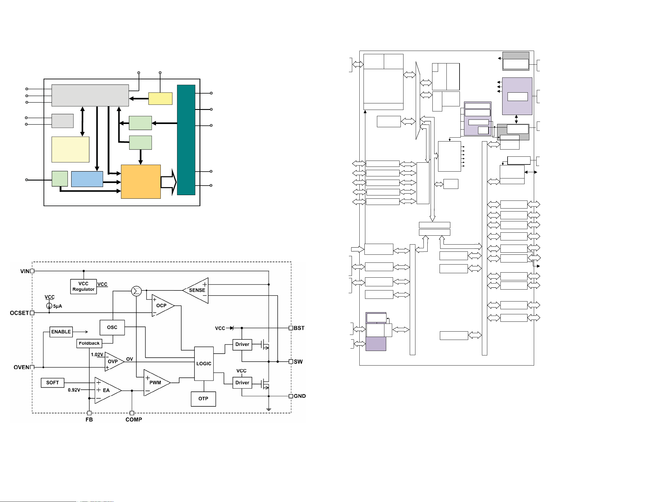
GTK-XB7
• IC Block Diagrams
– MAIN Board –
U1 LED1642GWTTR
SDI
CLK
LE
V
DD
GND
UVLO
& POR
Configuration
R-EXT
Current
Ref.
U3, 4 EUP3490
Control Logic &
Data Registers
register
Current gain
adjustment
SDO
Error
detection
Thermal
shutdown
Channel driver
Timing control
Turn ON/ OFF
Gradual delay
PWM
counter
PWCLK
16 output channels
OUT0
OUT1
OUT2
…………
OUT14
OUT15
U16 STM32F030R8T6
Serial
Wire
Debug
CORTEX-M0 CPU
= 48 MHz
f
HCLK
NVIC
5 channels
GPIO port A
GPIO port B
GPIO port C
GPIO port D
GPIO port F
EXT. IT
WKUP
SPI1
SPI2
SYSCFG IF
@ V
DDA
Te mp .
sensor
12-bit
ADC1
SWCLK
SWDIO
as AF
PA[15:0]
PB[15:0]
PC[15:0]
PD2
PF[1:0]
PF[7:4]
55 AF
MOSI,
MISO,
SCK,
NSS as AF
MOSI/MISO,
SCK/NSS,
as AF
AD inputs
V
V
DDA
16
SSA
GP DMA
IF
Bus matrix
AHB decoder
AHB
APB
Obl
Flash
interface
4 / 8 KB
SRAM
controller
RESET &
CLOCK
CONTROL
Flash
up to
64 KB,
32 bits
SRAM
CRC
WWDG
DBGMCU
TIMER 6
@ V
DDA
RC HS 14 MHz
RC HS 8 MHz
RC LS
PLL
AHBPCLK
APBPCLK
ADCCLK
USARTCLK
HCLK
FCLK
V
DD18
POR
Reset
Int
RTC interface
POWER
VOLT.REG
3.3 V TO 1.8 V
@ V
DD
SUPPLY
SUPERVISION
POR/PDR
@ V
DDA
@ V
XTAL OSC
4-32 MHz
IWDG
Power
Controller
@ VDD
XTAL32 kHz
RTC
TIMER 1
TIMER 3
TIMER 14
TIMER 15
TIMER 16
TIMER 17
USART1
USART2
I2C 1
I2C2
V
V
DD
NRST
V
V
OSC_IN (PF0)
OSC_OUT (PF1)
OSC32_IN (PC14)
OSC32_OUT (PC15)
TAMPER-RTC
(ALARM OUT)
= 2.4 to 3.6 V
DD
SS
DDA
DD
4 channels
3 compl. channels
BRK, ETR input as AF
4 ch., ETR as AF
1 channel as AF
2 channels
1 compl, BRK as AF
1 channel
1 compl, BRK as AF
1 channel
1 compl, BRK as AF
IR_OUT as AF
RX, TX,CTS, RTS,
CK as AF
RX, TX,CTS, RTS,
CK as AF
SCL, SDA, SMBA
(20 mA for FM+) as AF
SCL, SDA
as AF
GTK-XB7
4444
Page 45

GTK-XB7
U17 TAS5534
dnuorruS R 6MAdnaPAMWP
8MAdnaPAMWP
refoowbuS
CRSMWPSN
etalopretnI
eD
CD
CRD
Loud
tfoS
tfoS
7
0
dnuorruSL 5MAdnaPAMWP
tuoeniL R MWP
tuoeniLL MWP
DILAV
8
CRSMWPSN
etalopretnI
etalopretnI CRSMWPSN
8
hpmE
hpmE
kcolB
pmoC
loV
enoT
sdauqiB
teD
eD
CD
CRD
Loud
tfoS
tfoS
7
0
hpmE
eD
kcolB
kcolB
CD
CRD
2
pmoC
pmoC
Loud
8
tfoS
loV
loV
4
tfoS
enoT
enoT
sdauqiB
sdauqiB
8
7
teD
teD
0
CVSP
CVSP
2
lortnoC
emuloV
9
tnorF R 2MAdnaPAMWP
tnorFL 1MAdnaPAMWP
RM dnaPPH_MWP
LM dnaPPH_MWP
noitceS MWP
CRS MWPSN
etalopretnI
hpmE
eD
kcolB
CD
CRD
pmoC
rossecorP oiduAlatigiD
Loud
tfoS
loV
tfoS
enoT
sdauqiB
7
teD
0
CRSMWPSN
etalopretnI
eD
CD
CRD
Loud
tfoS
tfoS
7
0
hpmE
eD
kcolB
CD
pmoC
Loud
tfoS
loV
tfoS
enoT
sdauqiB
7
teD
0
CRSMWPSN
etalopretnI
hpmE
kcolB
8 2 Crossbar Mixer
CRD
pmoC
loV
enoT
sdauqiB
teD
retneC 7MAdnaPAMWP
Output Control
CRSMWPSN
CRSMWPSN
etalopretnI
etalopretnI
hpmE
hpmE
eD
eD
kcolB
kcolB
CD
CD
CRD
CRD
pmoC
pmoC
Loud
Loud
tfoS
tfoS
loV
loV
tfoS
tfoS
enoT
enoT
sdauqiB
sdauqiB
7
7
teD
teD
0
0
AVSS
AVD D
DVSS
DVDD
VRD_PLL
VRA_PLL
VBGAP
AVDD_REF
AVSS_PLL
AVDD_PLL
VR_PLL
ylppuS rewoP
Clock, PLL, and Serial Data I/F
KLCM
LF_LLP TP
LF_LLPTM
PAC CSO
8 8 Crossbar Mixer
lortnoC
eciveD
1NIDS
2NIDS
3NIDS
KLCRL
KLCS
8
DAP Control PWM Control
System Control
lortnoC
laireS
C
2
I/F
I
4NIDS
LCS
ADS
LES_PH
TESER
ETUM
NDP
RRE_DNKB
45
Page 46

GTK-XB7
U18 TAS5624A
/CLIP
/OTW
/FAULT
/RESET
MODE1-3
AVD D
VDD
AVD D
UVP
POWER-UP
RESET
TEMP
SENSE
BST_X
GVDD_X
AVDD
DVDD
DVDD
C_START
INPUT_A
INPUT_B
INPUT_C
PWM
RECEIVER
PWM
RECEIVER
PWM
RECEIVER
ANALOG
LOOP FILTER
ANALOG
LOOP FILTER
ANALOG
LOOP FILTER
DVDD
STARTUP
CONTROL
PROTECTION & I/O LOGIC
+
-
+
-
+
-
PWM &
TIMING
CONTROL
PWM &
TIMING
CONTROL
PWM &
TIMING
CONTROL
CB3C OVER-
LOAD
PROTECTION
GATE-DRIVE
GATE-DRIVE
GATE-DRIVE
BST_A
PVDD_AB
OUT_A
GND
GVDD_AB
BST_B
PVDD_AB
OUT_B
GND
BST_C
PVDD_CD
OUT_C
GND
INPUT_D
46
PWM
RECEIVER
ANALOG
LOOP FILTER
GVDD_CD
BST_D
PVDD_CD
+
-
PWM &
TIMING
CONTROL
GATE-DRIVE
OUT_D
GND
Page 47

U27 SRC4182
GTK-XB7
U32 SY8089
47
Page 48
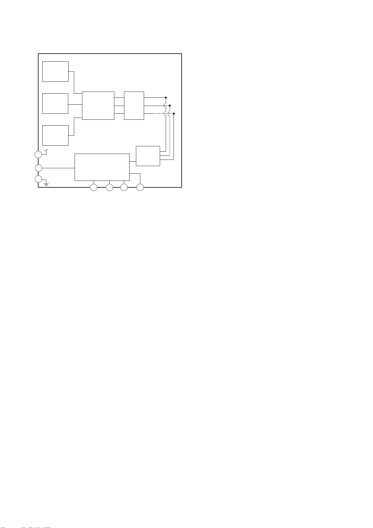
GTK-XB7
U35 KXCJK-1013
X
Sensor
Vdd
IO Vdd
GND
14
1
5
Y
Sensor
Z
Sensor
Charge
Amp
I2C
Digital Engine
4
6
A/D
Digital
Filter
117
48
Page 49

Note:
• -XX and -X mean standardized parts, so
they may have some difference from the
original one.
• Items marked “*” are not stocked since
they are seldom required for routine service. Some delay should be anticipated
when ordering these items.
5-1. SIDE PANEL SECTION
3
not supplied
not supplied
SECTION 5
EXPLODED VIEWS
• The mechanical parts with no reference
number in the exploded views are not supplied.
• Color Indication of Appearance Parts Example:
KNOB, BALANCE (WHITE) . . . (RED)
not supplied
top cover section
not supplied
Parts Color Cabinet’s Color
6
not
supplied
not supplied
GTK-XB7
The components identifi ed by mark 0
or dotted line with mark 0 are critical for
safety.
Replace only with part number specifi ed.
Les composants identifi és par une marque
0 sont critiques pour la sécurité.
Ne les remplacer que par une pièce portant le numéro spécifi é.
not supplied
not supplied
not supplied
not supplied
not supplied
not supplied
not supplied
not supplied
not supplied
not supplied
not supplied
4
1
not supplied
cabinet section
FFC1
not supplied
not supplied
not supplied
not supplied
not supplied
not supplied
not supplied
4
6
not supplied
2
not supplied
5
Ref. No. Part No. Description Remark Ref. No. Part No. Description Remark
1 9-885-209-50 SIDE PANEL (L UC2_BLACK)
2 9-885-209-48 SIDE PANEL (R UC2_BLACK)
3 9-885-209-56 RUBBER (CIRCLE BLACK) (4 pieces, 1 set)
4 9-885-209-57 RUBBER (SQUARE BLACK) (4 pieces, 1 set)
5 9-885-209-55 RUBBER (LARGE CIRCLE BLACK) (8 pieces, 1 set)
6 9-885-210-26 RUBBER (SMALL CIRCLE BLACK) (4 pieces, 1 set)
FFC1 9-885-209-33 FFC (TO MAIN)
49
Page 50
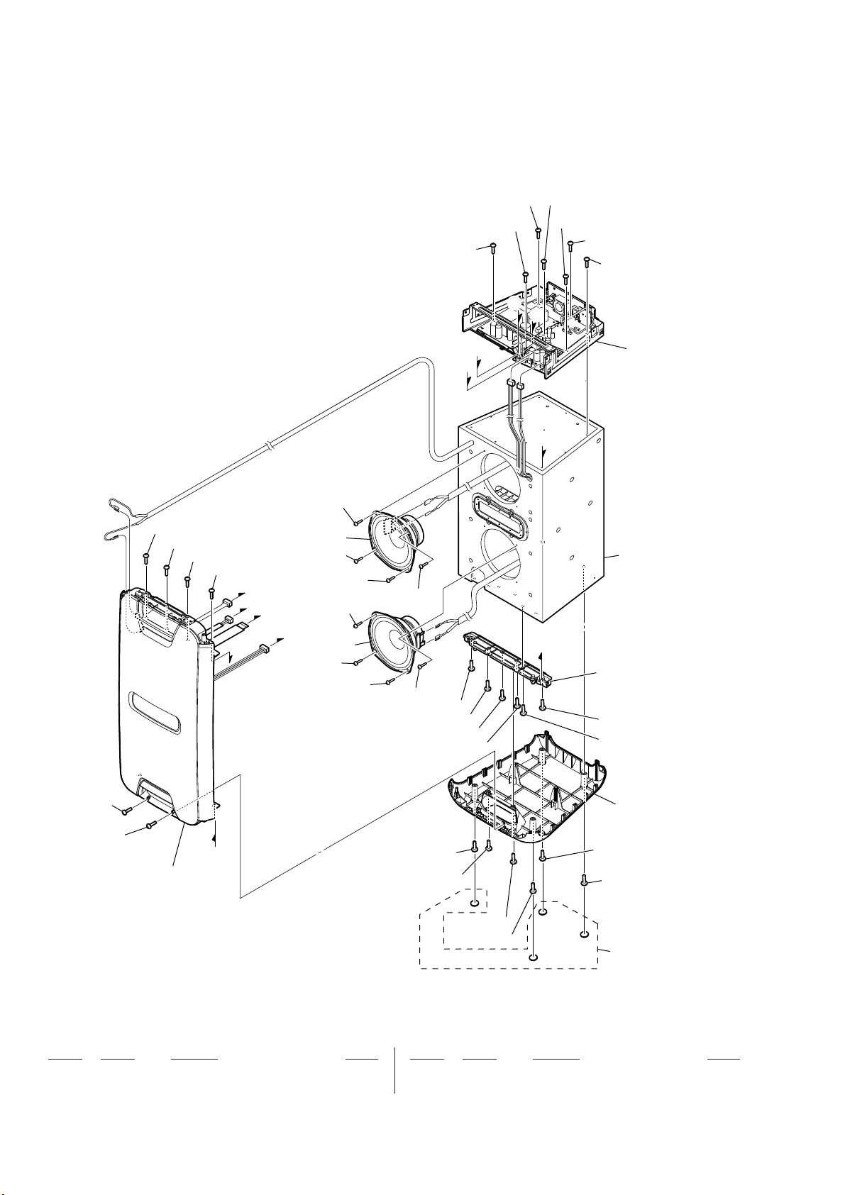
GTK-XB7
5-2. CABINET SECTION
not supplied
not supplied
not supplied
not supplied
A
B
E
not supplied
not supplied
not supplied
C
D
not supplied
SP2
not supplied
SP1
not supplied
not supplied
not supplied
not supplied
not supplied
not supplied
not supplied
D
not supplied
not supplied
not supplied
A
B
not supplied
not supplied
not supplied
not supplied
C
MAIN board section
E
not supplied
F
not supplied
not supplied
not supplied
not supplied
not supplied
front panel section
F
not supplied
not supplied
not supplied
not supplied
51
not supplied
not supplied
52
Ref. No. Part No. Description Remark Ref. No. Part No. Description Remark
51 9-885-209-52 BOTTOM COVER (BLACK) + PLATE
52 9-885-209-55 RUBBER (LARGE CIRCLE BLACK) (8 pieces, 1 set)
SP1 9-885-209-43 SPEAKER UNIT (WF) (160 mm) (Woofer)
SP2 9-885-209-43 SPEAKER UNIT (WF) (160 mm) (Woofer)
50
Page 51

5-3. TOP COVER SECTION
GTK-XB7
103
not supplied
not supplied
not supplied
not supplied
not supplied
not supplied
not supplied
102
FFC2
101
not supplied
not supplied
not supplied
Ref. No. Part No. Description Remark Ref. No. Part No. Description Remark
101 9-885-209-34 CONTROL BOARD, COMPLETE
102 9-885-209-32 BT&NFC BOARD, COMPLETE
103 9-885-209-47 TOP COVER (BLACK) + PLATE
FFC2 9-885-209-35 FFC (TO BT&NFC)
51
Page 52
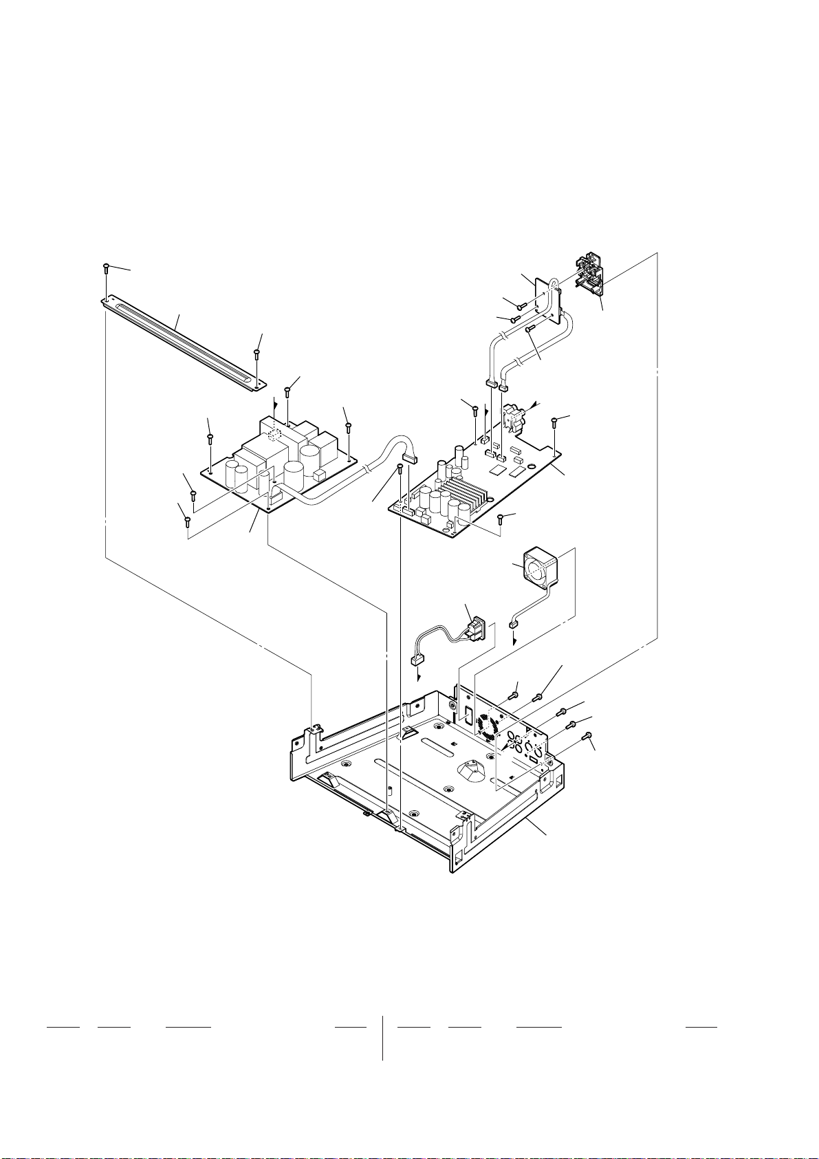
GTK-XB7
5-4. MAIN BOARD SECTION
not supplied
not supplied
not supplied
not supplied
not supplied
151
not supplied
not supplied
G
not supplied
not supplied
not supplied
not supplied
not supplied
not supplied
G
153
H
M1
not supplied
not supplied
not supplied
I
not supplied
152
not supplied
H
not supplied
not supplied
not supplied
I
not supplied
Ref. No. Part No. Description Remark Ref. No. Part No. Description Remark
151 9-885-209-29 PSU BOARD, COMPLETE
152 9-885-209-27 MAIN BOARD, COMPLETE
153 9-885-209-45 USB + KEY BOARD, COMPLETE
0 M1 9-885-209-46 FAN UNIT
not supplied
52
Page 53
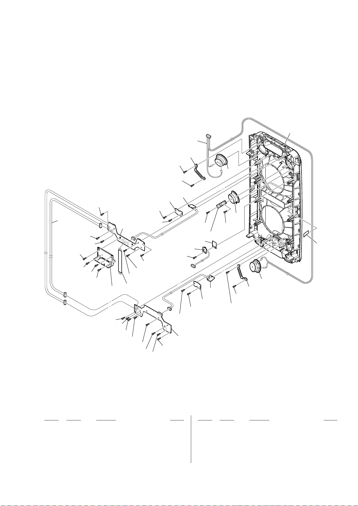
5-5. FRONT PANEL SECTION
• Rear view
GTK-XB7
206
not supplied
not supplied
not supplied
SP3
not supplied
WR1
not supplied
not supplied
not supplied
not supplied
not supplied
not supplied
not supplied
not supplied
not supplied
not supplied
201
not supplied
not supplied
not supplied
not supplied
not supplied
not supplied
not supplied
not supplied
not supplied
FFC3
not supplied
not supplied
not supplied
not supplied
203
not supplied
not supplied
not supplied
205
not supplied
not supplied
202
not supplied
204
not supplied
SP4
not
supplied
SP5
not supplied
not supplied
not supplied
Ref. No. Part No. Description Remark Ref. No. Part No. Description Remark
201 9-885-209-38 LA BOARD, COMPLETE
202 9-885-209-39 LB BOARD, COMPLETE
203 9-885-209-36 RGBE BOARD, COMPLETE
204 9-885-209-37 RGBF BOARD, COMPLETE
205 9-885-209-42 IR BOARD, COMPLETE
206 9-885-209-53 FRONT PANEL (UC2 BLACK) ASSY
FFC3 9-885-209-40 FFC CABLE
SP3 9-885-209-44 SPEAKER UNIT (TW) (50 mm) (Tweeter)
SP4 9-885-209-44 SPEAKER UNIT (TW) (50 mm) (Tweeter)
SP5 9-885-209-44 SPEAKER UNIT (TW) (50 mm) (Tweeter)
WR1 9-885-209-41 CABLE
53
Page 54

GTK-XB7
SECTION 6
ACCESSORIES
Ref. No. Part No. Description Remark
4-582-492-11 MANUAL, INSTRUCTION
(ENGLISH, FRENCH, SPANISH)
501 1-493-170-11 REMOTE COMMANDER (RMT-AM200U)
0 502 9-885-209-81 AC CORD (UC2) (AC power cord)
(Remote control)
501 502
The components identifi ed by mark 0
or dotted line with mark 0 are critical for
safety.
Replace only with part number specifi ed.
Les composants identifi és par une marque
0 sont critiques pour la sécurité.
Ne les remplacer que par une pièce portant le numéro spécifi é.
54
Page 55

MEMO
GTK-XB7
55
Page 56

GTK-XB7
REVISION HISTORY
Ver. Date Description of Revision
1.0 2016.01 New
 Loading...