

Page 1
SERVICE MANUAL
MODEL COMMANDER DEST. CHASSIS NO.
FDL-PT22
FDL-PT22/JE
US
JE
MODEL COMMANDER DEST. CHASSIS NO.
∗ Please file according to model size. ....
2.2
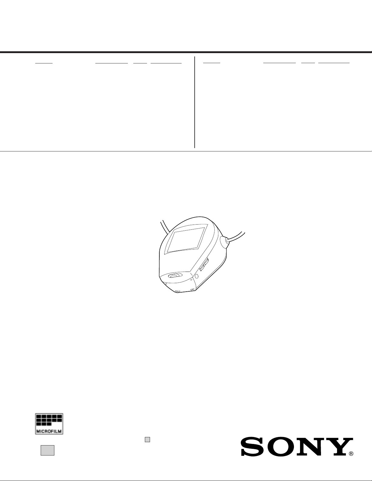
LCD COLOR TV
Page 2

SPECIFICATIONS
TV standerd American TV standerd
Channel converage
VHF : 2-13
UHF : 14-69
Antenna VHF/UHF strap antenna
Display format
Transmission type TN liquid crystal
panel
Drive format Passive matrix
Picture 2.2 inches measured diagonally
Output Headphones : minijack
Impedance 8 - 45 ohms
Power requirements 4.5 V DC
Power consumption Approx : 2.9W
Speaker Ø28 mm (1 1/8 in.), 0.1 W
Temperature range 32 ˚F - 104 ˚F (0 ˚C - 40 ˚C)
Dimensions Approx. 91x109x64mm (w/h/d)
(3 5/8 x 4 3/8 x 2 5/8 in.) excl.
Projecting parts and controls
Strap length Approx. 1,300 mm (51 1/4 in.)
Mass Approx. 230 g (8.1 oz), excl. batteries
Design and specifications are subject to change without notice.
Optional accessories
AC power adaptor AC-E45HG / External antenna cord EAC39 /EAC-110/Size AA (LR6) alkaline battery
SAFETY-RELATED COMPONENT WARNING!!
COMPONENTS IDENTIFIED BY SHADING AND MARK ¡ ON THE
SCHEMATIC DIAGRAMS, EXPLODED VIEWS AND IN THE P ARTS
LIST ARE CRITICAL TO SAFE OPERATION. REPLACE THESE
COMPONENTS WITH SONY P ARTS WHOSE P ART NUMBERS APPEAR AS SHOWN IN THIS MANUAL OR IN SUPPLEMENTS PUBLISHED BY SONY.
– 2 –
Page 3

TABLE OF CONTENTS
Section Title Page Section Title Page
1. GENERAL ....................................................................... 4
2. DISASSEMBLY
2-1. Cabinet Removal ..................................................... 6
2-2. Service Position....................................................... 7
3. CIRCUIT ADJUSTMENTS
3-1. A Board Adjustment................................................ 8
3-2. T Board Adjustment ................................................ 8
3-3. B Board Adjustment................................................ 9
4. DIAGRAMS
4-1. Block Diagram ........................................................ 11
4-2. Circuit Boards Location .......................................... 15
4-3. Printed Wiring Boards and Schematic Diagrams.... 15
• T Board .................................................................. 17
• A Board.................................................................. 21
• B Board.................................................................. 25
4-4. Semiconductors ....................................................... 29
5. EXPLODED VIEW
5-1. Chassis..................................................................... 30
6. ELECTRICAL PARTS LIST...................................... 31
– 3 –
Page 4
– 4 –
A
a
22
22
2
11
11
1
AA(LR6) × 3
b
DC IN 4.5V
c
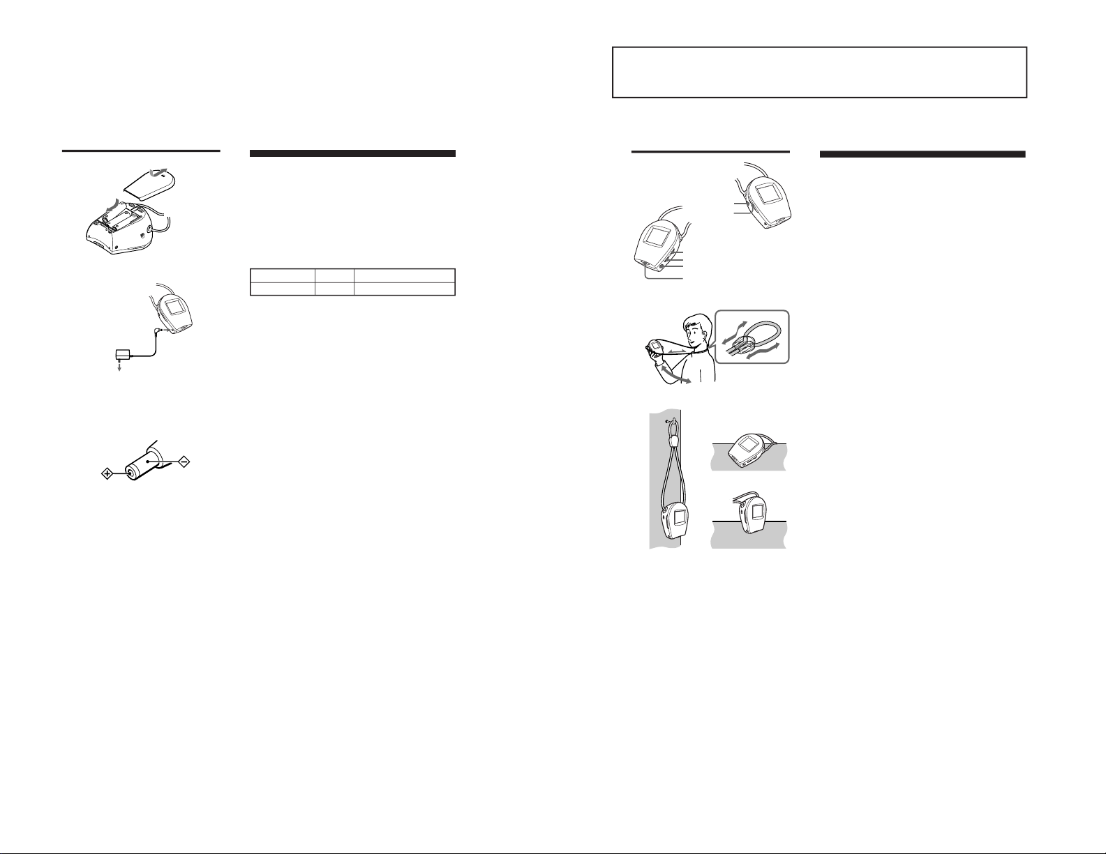
Power Sources (see fig. A)
Alkaline Batteries
Use Sony LR6 alkaline batteries (not supplied).
1
Push and slide the battery cover open.
2
Insert three batteries. Be sure to insert the (–) polarity
of each battery first as illustrated.
Battery Life: With continuous use, Sony LR6 alkaline
batteries will last about 3.0 hours.
Battery Type Size Battery Life
LR6 AA Approx. 3.0 hours
Note
When the picture becomes dim or the tuning does not lock
onto a channel, replace all the batteries with new ones.
House Current
See fig. A–b.
Note
Use only the recommended AC power adaptor, AC-E45HG
(not supplied). (For the polarity of the plug, see fig. A–
c).
to a wall outlet
Polarity of the plug
OFF/VHF/UHF
EXT ANT
CH +/–
VOL
BRT
2
B
a
b
Operation (see fig. B)
1
Set the OFF/VHF/UHF switch to VHF or UHF
whichever band you want to watch.
2
Press the CH +/– button to select a channel.
3
Adjust the volume with the VOL dial.
4
Adjust the brightness with the BRT dial.
To switch off the TV: Set the OFF/VHF/UHF switch to
OFF.
To improve the broadcast reception: Extend the strap
antenna and move the unit in every direction.
Note
If strong pressure or stress is applied to the antenna strap,
it automatically disconnects from the TV for safety.
Contact your nearest Sony dealer or authorized service
center for its repair.
There may be poor broadcast reception in the
following areas:
• Faraway from the broadcasting station, or behind a
mountain or tall building.
• Inside a train or car, etc.
• Where there strong interference, such as near a high
tension wire, neon sign, or radio station.
• Near a railway line or expressway, or under the air traffic
routes.
• In the underground shopping centers, tunnels, or solid
buildings.
Listening with headphones: Connect headphones (not
supplied) to the 2 (headphones) jack. The sound is heard
from both sides of the headphones, but the sound is
monaural.
How to use the TV
Wear the TV around your neck. You can adjust the length
of the strap. (See fig. B–a).
You can also suspend or place the TV on a flat surface. (See
fig. B–b).
SECTION1
GENERAL
The operating instructions mentioned here are partial abstracts from the
Operating Instruction Manual. The page numbers of the Operating Instruction Manual remein as in the manual.
Page 5
– 5 –
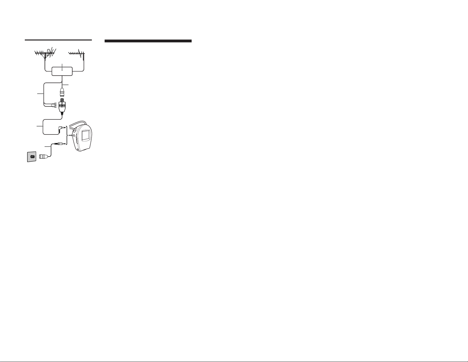
C
VHF
UHF
e
d
c
b
a
a Mixer
b 75Ω coaxial cable
c Feeder
d EAC-39 antenna cable (not
supplied)
e EAC-110 antenna cable (not
supplied)
External Antenna Connection
(see fig. C)
Connect an antenna cord EAC-39 (not supplied) or EAC110 (not supplied) to the TV. This will improve the TV’s
reception.
To EXT ANT
Page 6
SECTION 2
DISASSEMBLY
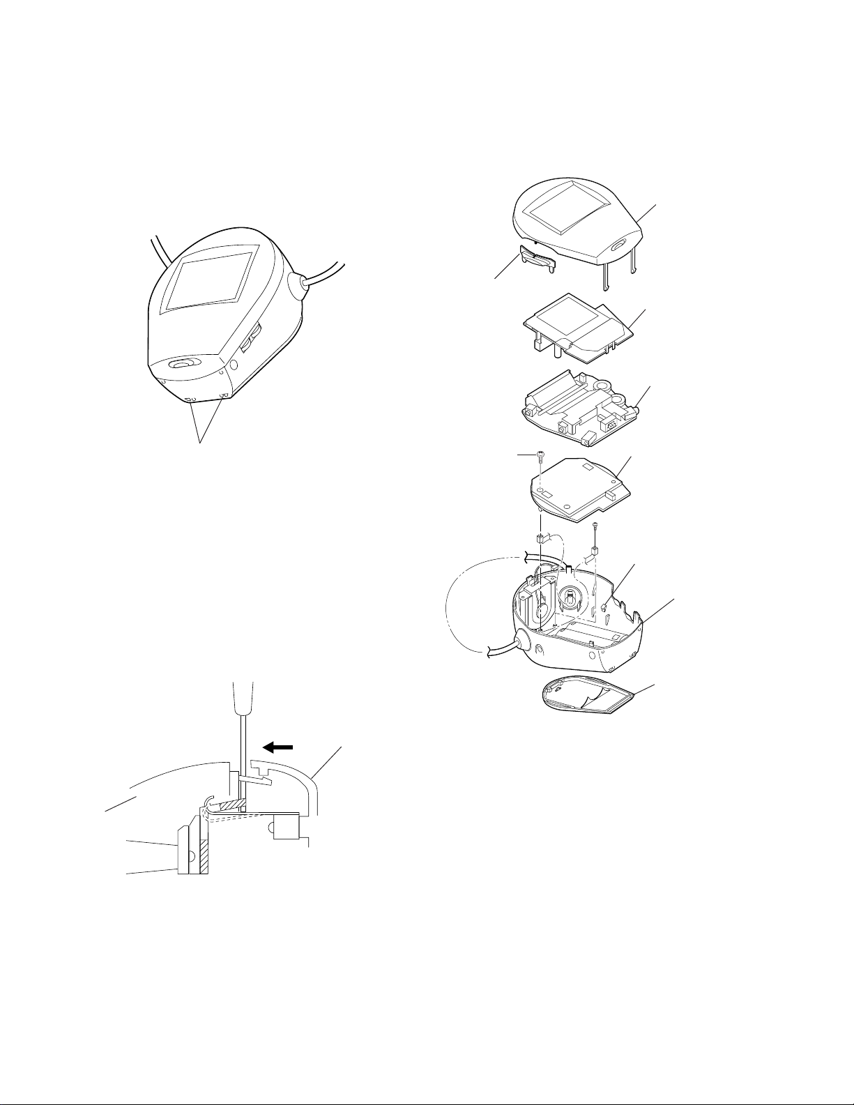
2-1. CABINET REMOVAL
1. Remove battery cover 8.
2. Push the two hooks in the lower section of the rear cabinet with
a pint and the like to undo them.
Hooks
2Channel
button
1Screw
(+P2 x 10)
1Front cabinet
assy
3 B board
4A board
5T board
3. While pressing the rear cabinet, undo hooks on the periphery.
4. Insert a pin into the upper side of the cabinet, and while pushing the hook, tilt the pin to the rear cabinet side.
5. Remove the channel button 2.
6. Remove the speaker cord from the connector.
7. Remove B board 3 and A board 4.
8. Remove one screw 6 (+P x 10) from T board 5.
9. Remove T board 5 from the hooks (one each on both side) on
the rear cabinet.
Front cabinet
Rear cabinet
Claw
7Rear cabinet assy
8Battery cover
– 6 –
Page 7
2-2. SERVICE POSITION
Service cord
1-900-211-84
CN602
A board
CN601
Service cord
1-900-211-84
B board
AC Power
adapter
AC-E45HG
CN301
J101
Mini jack
T board
CN201
Antena
– 7 –
Page 8

SECTION 3
CIRCUIT ADJUSTMENT
3-1. A BOARD ADJUSTMENT
+4.5V ADJUSTMENT
Measure the voltage between JL32 (4.5V) and JL33 (GND) with a
digital voltmeter, and adjust RV601 so that the voltage will be as
follows:
<Specification>
4.45 ± 0.05VDC
S601: UHF position
CONFIRMATION OF +30V
Measure the voltage between JL29 (30V) and JL33 (GND) with a
digital voltmeter, and adjust RV601 so that the voltage will be as
follows:
<Specification>
30.5 ± 1.5VDC
CONFIRMATION OF AUDIO OUTPUT
(1) Input 1kHz voice, 100% modulation from sound generator.
(2) Make RV501 MAX.
(3) Connect the probes of an oscilloscope to JL23 (SP) and JL15
(SP GND).
(4) Check the waveform on the oscilloscope, and make sure that it
is within the standard.
<Specification>
1.5 - 2.8Vp-p
3-2. T BOARD ADJUSTMENT
- T BOARD - (COMPONENT SIDE)
RV004
RV001
RV002
RV201
TU101
ROUGH ADJUSTMENT OF VIF.AFT
(1) Preparation
Set S601 in the VHF position.
Make JL18 (RF) signal-less
Insert 1kΩ between JL77 (4.5V) and JL28 (RF AGC).
Input a sweep signal to the section between JL26 (IF) and JL27
(IF GND).
Sweep signal
75
Fig.3-1
ATT
¶
0.01µF
6dBfo 45.75MHz}5kHz
JL26
Note: The sweep signal level should be -30 ± 5dBm at JL26.
The distance between the ATT output and JL26
should be as short as possible.
(2) Insert the output between JL72 (VIDEO) and JL71 (A.GND)
to an oscilloscope, and apply external voltage (MGC) to JL51
so that the waveform shown in Fig.3-2 will appear (the minimum section should not clip). Adjust T202 so that the position
of 45.75MHz will be the lowest.
Note: This portion should be approx. 1.0Vp-p when exter-
nal voltage is applied to JL51 (MGC).
The external voltage applied to JL51 (MGC) should
not exceed 4.3VDC.
– 8 –
Page 9

RF.AGC ADJUSTMENT
p
Approx. 1.0V
45.75MHz
Fig.3-2
(3) Remove the external voltage (MGC) from JL51.
(4) Connect the output between JL31 (AFT) and JL30 (D.GND) to
an oscilloscope, and roughly adjust T201 so that the position
of 45.75MHz will be a zero cross.
(5) Remove 1kΩ from the section between JL77 (4.5V) and JL28
(RF AGC).
(1) Input the VHF color bar signal from the test signal generator.
(2) Adjust RV201 to optimum position so that there is no snow
noise on the screen.
CHANNEL DISPLAY POSITION ADJUSTMENT
(1) Set S601 in the VHF position.
Insert resistors (47kΩ + 15kΩ) between JL25 and JL77 (4.5V
line), and short circuit JL21 and JL30 (D.GND).
(2) Receive 2ch, and adjust the channel display position with
RV002.
(3) Receive 13ch, and adjust the display bar with RV004.
(4) Carry out tracking, because (2) and (3) interfere with each other.
(5) Receive 6 and 7ch, and check that the display bar conforms to
the standard.
(6) Set S601 in the UHF position.
(7) Receive 14ch and adjust the display position with RV001.
(8) Receive 40ch and 69ch, and check that the display bar con-
forms to the standard.
(9) Remove resistors from JL25 and JL77, and open the short cir-
cuit between JL21 and JL30
JL25
AFT ADJUSTMENT
(1) Insert 1kΩ between JL77 (4.5V) and JL28 (RF AGC).
Note: Because of drifting due to aging, adjustment should
be made at the end of the process.
(2) Switch the sweep signal to CW.
fo = 45.75MHz ± 5kHz
Input the above signal to the section between JL26 (IF) and
JL27 (IF GND), and finely adjust T201 so that the level between JL31 (AFT) and JL30 (D.GND) will be 2.2 ± 0.4VDC.
(3) Remove 1kΩ from the section between JL77 (4.5V) and JL28
(RF AGC).
15K
47K
JL77
Display bar
Channel No.
6
*Channel No. and display ber are to be in line.
Fig.3-3
– 9 –
Page 10

3-3. B BOARD ADJUSTMENT
HUE ADJUSTMENT
- B BOARD - (COMPONENT SIDE)
RV301
RV402
GRADATION ADJUSTMENT
(1) Input a 10-step staircase signal from the test signal generator.
(2) Connect an oscilloscope probe between JL83 (G) and JL67 (D.
GND) and observe the waveform.
(3) The contrast should change when RV402 is turned.
(4) Connect the oscilloscope prove between JL84 (AUTO CB) and
JL67 (D. GND), and observe the waveform. Adjust RV402 so
that voltage A is 2.2±0.2V
(5) Check that the waveform between JL84 and JL67 is as shown
in Fig.3-4.
(6) Check to see that the phases C and D are within the range speci-
fied (↔).
(1) Receive a color bar.
(2) Insert an oscilloscope between JL81 (B) and JL67 (D.GND).
(3) Arrange RV301 as shown in Fig.3-5.
Fig.3-5
JL83
0 IRE
JL84
100 IRE
Picture contrast
is varies.
D
C
A = 2.2 ± 0.2V
Fig.3-4
– 10 –
Page 11
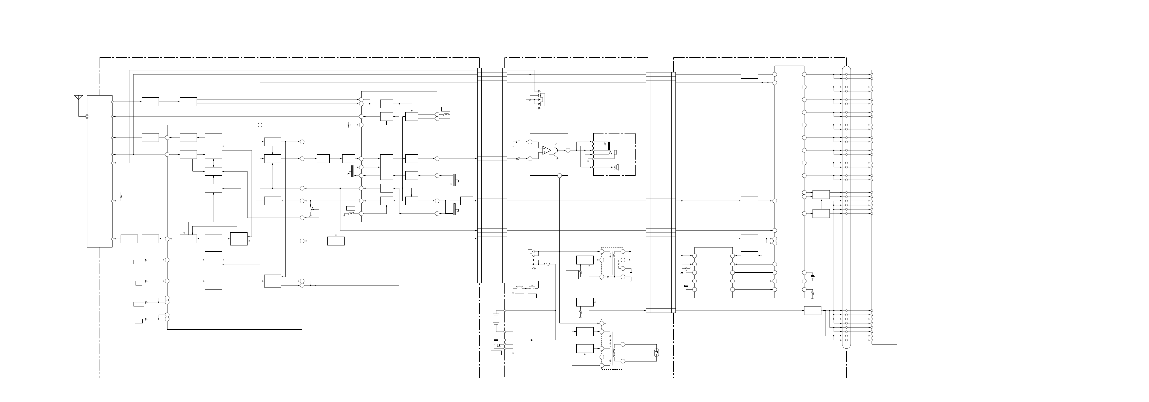
4-1. BLOCK DIAGRAM
IF
TU101
AGC
TUNER
RF IN
BS
VB
UB
+4.5V
MB
SECTION 4
DIAGRAMS
IF AMP
Q201
IC001 TUNER CONTROL
SW
Q006
28
27
BS
U/V
FILTER
SWF201
BS
COMPOSITION
BAND
SELECT
TUNING
CONTROL
BAND
SELECT
AUTO
RETURN
3
HP
DEFEAT
OUTPUT
SIGNAL
DEFECT
COMPARATOR
DEF
FH
H SYNC
AFC
SUD
14
IC401
MONITER CONTROL
4037R2
HSO
CP
CL2
CLB
CLA
D2
1
2
3
4
5
CP
CP
CL2
CL2
CLB
CLB
CLA
CLA
D2
D2
24
40
22
38
21
37
20
36
12
28
IF
6
IF
7
AGC OUT
3
AGC DL
4RV201
IC201 VIF/SIF DET
IF AMP
AGC IF
VIDEO
DET
REF COIL
REF COIL
19
20
LLD
CN201 CN502
UB 1212
VHF
H.P
2
3
2
3
+4.5V
S601
(1/2)
CN601 CN301
VHF
H.P
2
3
2
3
BUFFER
Q403
IC501 HP AMP
11
D3
D4
D1
BESTB
TPR1B
DB 10
6
7
8
9
12
13TPR1
VM BUFFER
Q407
SW
Q406
3
1
4
5
6
FH SW
Q005
Q007
AFC SW
INV
Q205
CF202
AFT
E-VDL
14
FM DET
15
LIM
16
SYNC
23
AFT
17
AFT COIL
21
FM
DET
SYNC
SEP
AFT
BUFFER
LIMITER 10
VIDEO
AMP
AUDIO
SIF
DET OUT
SYNC SEP
13
18
22
CF203
CF201
BUFFER
Q202
AUDIO
5
VIDEO
9
RV501
5
9
2
VCC
V+
J501
6
7
PHONES
SPEAKER
VIDEO
9
9
SYNC SEP
Q303
34
V IN
D3
D3
D4
D1
D1
RES
RES
TPR2
TPR1
VM
VM
VM
VSS
27
10
26
25
13
29
23
39
9
2
6
4
3
LCD
MONITOR
TV
BUFFER
Q001
RV001
U LOW
RV003
UA
RV002
V LOW
RV004
V HI
AMP
Q002
26
18
22
20
19
23
24
BT
UP
UA
VLP
VHP
VHA
VLA
BT
GEN.
INITIAL
BAR
DISPLAY
POSITION
ADJUST
T(TUNER,VIF/SIF DET,TUNING)
SET
CHARGE/
DISCHARGE
CIRCUIT
BA R
OUTPUT
CS
H SYNC
7
10
V
30
U
31
INV/SW
Q003,004
8
UP DOWN SW 1111
IND
BATTERY
J701
DC IN
7
8
S601
(2/2)
S001 S002
DOWN
F601
+4.5V
UP
D701
A(DC IN,B/L INV)
RV601
PORT SW
Q610
RV450
PORT SW
Q601-603
BUFFER
Q401
DRIVE
Q701
DRIVE
Q702
9
8
4
+30V
3
2
4
1
5
T601
T701
H SYNC
7
IND
7
88
IND SW
Q408
IC301 Y/C/J
1
+30V
6
+4.5V
7
3
11 11BRT
8
BACK
LIGHT
6
RV301
3.58MHz
VIDEO IN
29
SYNC SEP
19 10
TINT CONT
21 11
VCXO IN
23 12
VCXO OUT
X301
HD IN
CONTRAST
R OUT
G OUT
B OUT
INV
51
Q302
35 H IN
38 INB
R40
AUTO CB
23
R IN
28
G IN
29
27
B IN
XT1
XTD
20
21
30TGL VL
4.5MHz
RV402
BUFFER
Q402
X401
VDG
VDR
VDG
VDR
VDB
VDB
VS2
VS2
17
18
33
34
16
32
15
31
B(HP AMP,MONITOR CONTROL,CHROMA)
– 11 –
– 12 –
– 13 –
– 14 –
Page 12

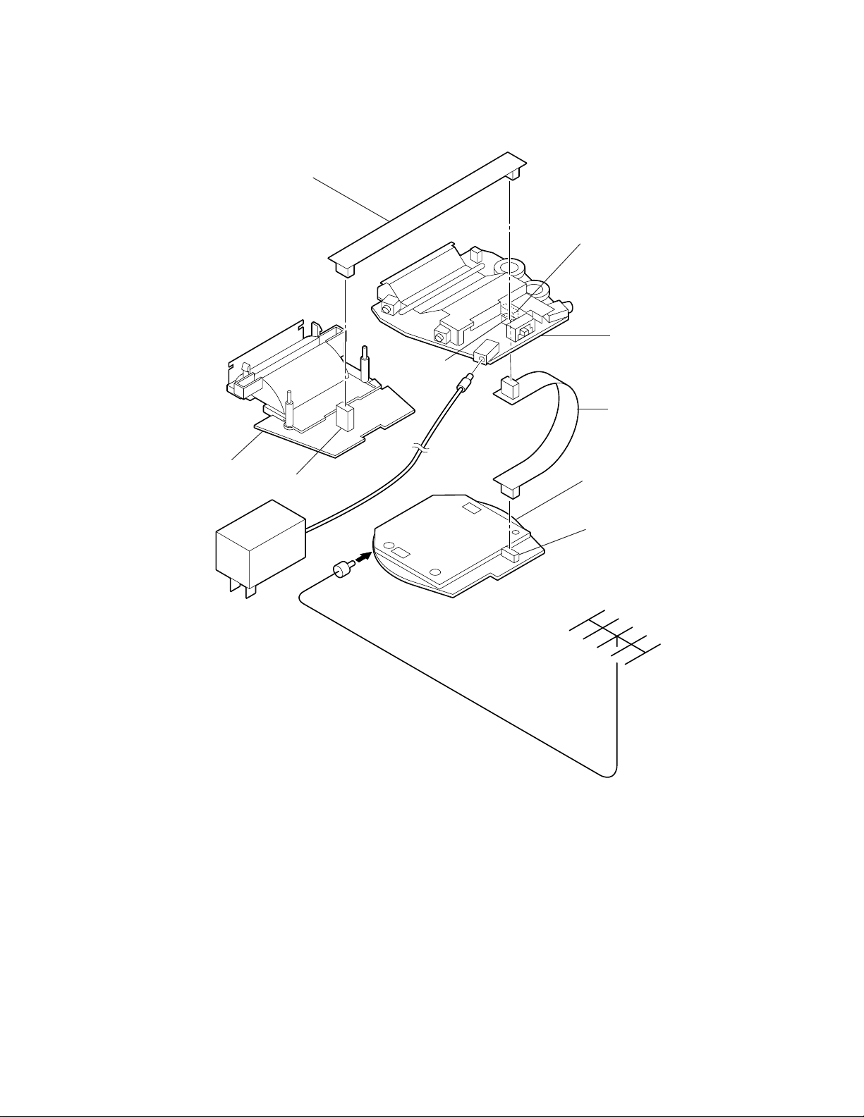
4-2. CIRCUIT BOARDS LOCATION
B
T
A
4-3. PRINTED WIRING BOARDS AND SCHEMATIC
DIAGRAMS
Note:
• All capacitors are in µF unless otherwise noted. pF : µµF 50WV or less are not
indicated except for electrolytics and tantalums.
• All electrolytics are in 50V unless otherwise specified.
• All resistors are in ohms.
kΩ=1000Ω, MΩ=1000kΩ
• Indication of resistance, which dose not have one for rating electrical power , is
as follows.
Pitch : 5mm
Rating electrical power :
: internal component.
•
: panel designation and adjustment for repair.
•
1
/
W (CHIP : 1/10W)
4
• All variable and adjustable resistors have characteristic curve B, unless otherwise noted.
•As to the voltage volue shown by the semiconductors on the Shematic Diagram, see the another list
• Readings are taken with a color-bar signal input.
• Readings are taken with a 10MΩ digital multimeter.
• V oltages are dc with respect to ground unless otherwise noted.
• V oltage variations may be noted due to normal production tolerances.
• All voltages are in V.
: Measurement impossibillity.
*
v
•
•
: B+line.
: signal path.
• Circled numbers are waveform references.
Reference information
RESISTOR : RN METAL FILM
: RC SOLID
: FPRD NONFLAMMABLE CARBON
: FUSE NONFLAMMABLE FUSIBLE
: RW NONFLAMMABLE WIREWOUND
: RS NONFLAMMABLE METAL OXIDE
: RB NONFLAMMABLE CEMENT
:
ADJUSTMENT RESISTOR
COIL : LF-8L MICRO INDUCTOR
CAPACIT OR : TA TANT ALUM
: PS STYROL
: PP POLYPROPYLENE
: PT MYLAR
: MPS METALIZED POLYESTER
: MPP METALIZED POLYPROPYLENE
: ALB BIPOLAR
: ALT HIGH TEMPERATURE
: ALR HIGH RIPPLE
Note: The components identified by shading and mark ¡
are critical for safety. Replace only with part number
specified.
Terminal name of semiconductors in silk screen
printed circuit ( )
Device Printed symbol Terminal name
Transistor
1
Transistor
2
3
Diode
4
Diode
Diode
5
Diode
6
Diode
7
8
Diode
Diode
9
Diode
0
Diode
!¡
Diode
!™
Transistor
!£
(FET)
Transistor
!¢
(FET)
Transistor
!∞
(FET)
Transistor
!§
Transistor
!¶
Transistor
!•
Transistor
!ª
Transistor
@º
Transistor
@¡
Transistor
@™
Transistor
@£
Discrete semiconductot
–
(Chip semiconductors that are not actually used are included.)
Collector
Base
Collector
Base
Cathode
Cathode
Anode
Cathode
Anode
Common
Anode
Common
Anode Cathode
Common
Anode
Common
Anode Anode
Common
Cathode
Common
Cathode
Anode
Anode
Cathode
Drain
Drain
B1 E1C2
B2 C1E2
B2 E2C1
B1 C2E1
B2 E2C1
B1 C2E1
B2 E2C1
B1 C2E1
E2
B1 E1
(B2)
E1
B1
(B2)
E1
E2
Emitter
Emitter
Anode
(NC)
(NC)
Cathode
Anode
Cathode
Cathode
Cathode
Anode
Anode
Source
Gate
Source
Gate
Source
Drain
Gate
Emitter
Collector
Base
C1(B2)C2
E2
C2C1
B1
C1C2
Circuit
D
G
D
S
B1
B1
B1
B1
B1
B1
D
G
S
S
D
G
C1
E1
C1
E1
E1
C1
E2
C1
C1
G
S
C2
B2
E2
C2
B2
E2
E2
B2
C2
C2C1(B2)
E2
E2E1(B2)
C2
C2E1(B2)
C2
Ver.1.5
T BOARD IC VOLTAGE LIST
Pin Volt Pin Volt Pin Volt
IC001 1 2.7
20
3 0.3
4 0.5
5 2.5
6 2.5
7 2.5
8 4.3
910 0.7
11 2.5
12 0
13 0.3
14 0.0
15 3.7
16 17 18 0
19 2.2
20 2.2
21 2.9
22 0.8
23 2.1
24 2.1
25 26 1.7
27 3.8
28 0
29 GND
30 0
31 0
32 0
IC201 1 3.4
2 3.4
3 1.6
4 3.3
5 4.2
6 3.4
All voltage are in V.
T BOARD TRANSISTOR
VOLTAGE LIST
BCE
Q003 0 3.7 GND
Q004 3.7 0.7 4.3
Q007 2.6 0.5 4.3
Q201 1.0 4.2 0.3
Q202 1.9 GND 2.6
Q203 0 3.5 GND
123456
Q002 0 1.7 2.2 29.5 1.7 2.2
Q006 1.2 1.2 GND 0 0 GND
All voltage are in V.
7 3.4
8 GND
9 4.3
10 1.6
11 1.6
12 GND
13 1.8
14 3.5
15 2.1
16 1.5
17 2.4
18 2.0
19 1.9
20 1.9
21 3.4
22 3.4
23 0.4
24 1.7
- : Not used
A
B
C
D
E
G
H
1 2 3 4 5 6 7 8 9 10 11 12 13 14 15
J101
TU101
TEPA5
G
4.5V
R012
330k
:CHIP
C011
10
16V
:7L
D001
MA152WK-TX
RV001
47k
:CHIP
2
ULOW
RV002
3
F
I
R020
470k
J
:CHIP
47k
:CHIP
VLOW
2SB709A-R
R019
270k
:CHIP
4
5
6
1
RV004
VHI
100k
:CHIP
Q001
R008
270k
:RN-CP
4.5V
R022
47k
:CHIP
1
3
CH:CHIP
R030
0
:CHIP
30V
6
R009
33k
:RN-CP
R024
47k
:CHIP
2
Q006
XN4215
C003
560p
R002
100k
:CHIP
R004
:CHIP
4
5
R003
68k
:CHIP
47k
1
3
C018
1
16V
F:CHIP
BRT
1718192021222324
UP
VHP
VLP
CON
UA
VHA
VLA
R005
150k
:CHIP
Q002
XN4601
2
C012
1
16V
F:CHIP
TV
UB
AGC
ANT
C106
C108
C105
C107
0.001 B:CHIP
0.1 F:CHIP
0.001 B:CHIP
C001
4.7
25V
:7L
14
15
16
NC
DEF
CHCAL
IC001
AN5707NFAP
NCBTU/VBSGND
25262728293031
VB
BS
C109
0.001 B:CHIP
0.001 B:CHIP
R001
100k
:CHIP
C002
47
6.3V
:7L
12
13
STOP
MANU
IF
MB
C110
0.001 B:CHIP
10
11
CS
CHA
V OUT
U OUT
R011
10k
:CHIP
R111
22
:CHIP
R031
82k
:CHIP
Q004
UN2110-TX
9
NC
VCC
UH
SUD
AFC
HSYNC
H.P
2
M.M
1 2 3 4 5 6 7 8
FH
NC
32
30V
Q007
UN211D-TX
UN2210-TX
D002
MA157-TX
R016
39k
:CHIP
C014
0.1 25V F:CHIP
C007
0.001 B:CHIP
R017
18k :CHIP
C008
0.47
25V
F:CHIP
IF
Q003
R021
100k
:CHIP
R013
56k :CHIP
C021
0.01
B:CHIP
F:CHIP
C004
47
6.3V
:7L
C016
F:CHIP
R029
470
:CHIP
C005
0.01
B:CHIP
R014
39k
:CHIP
C006
0.1
25V
R010
2.2
:CHIP
R018
100k
:CHIP
0.1
25V
IF
ELECTRONIC TUNER
VIF,SIF
Q201
2SC3837KT146Q
L205
0.82µH
R216
R218
68
:CHIP
C210
0.01
B:CHIP
4.5V
:FR-CP TSF1226L
1.2k
:CHIP
R219
390
:CHIP47:CHIP
R214
1k
:CHIP
C209
0.01
B:CHIP
C211R220
0.01
B:CHIP
T
I
1
3
GOO
R215
10
:CHIP
SWF201
SWF
2
4
4.5V
IF
R217
1k :CHIP
IF
4.5V
L206
1µH :FR-CP
4.5V
C235
0.001
B:CHIP
T201 T202
45.75MHZ 45.75MHZ
AFT
1
2
34
C207
10p
CH:CHIP
C208
2p
CK:CHIP
ADJ
IF AGC
SYNC OUT
AGC
AGC
FILTER OUT
FILTER IN
1 2 3 4 5 6 7
R223
1k
:CHIP
R226
2.2k
:CHIP
1
C219
1
4.5V
R243
22k
:CHIP
R222
8.2k
:CHIP
C222
10
16V
:7L
R225
3.9k
:CHIP
6
C223
C224
0.01
B:CHIP
C234
0.01
B:CHIP
R242
470
:CHIP
3 4
LLD
R241
180k
:CHIP
6
1
2
31
SYNC SEP
AFT COIL
REF COIL
M51348AFP
OUT
RF AGC
(VIF)
RF AGC
VCC
DELAY
C215
47
6.3V
:7L
C225
C226
0.01 B:CHIP
0.01 B:CHIP
R230
10
:CHIP10:CHIP
L201
15µH
:FR-CP
R202
270
:CHIP
CF201
TPS4.5MC
VIDEO
R209
1.8k :CHIP
DET OUT
REF COIL
IC201
IF IN
IF IN
IF
IF
R224
1.5k
:CHIP
RV201
1k
:CHIP
R229
10k
:CHIP
R231
C202
0.01
B:CHIP
VIDEO VIDEO
12
R240
10k
:CHIP
3
3
21
CF202
CD4.5MC
OUT
LIMITER
FM DETIN
(SIF)
VCC
SIF IN
109 11 12
SIF
21
CF203
SFSL4.5MC
C205
R206
10
16V
1.8k :CHIP
:7L
C206
27p CH:CHIP
E-VDL
DC F/B
3
C218
0.01
B:CHIP
C203
R205
100k :CHIP
R212
R210
33k :CHIP
AFT OUT
(VIF)
GND
8
C212
0.1 25V F:CHIP
680 :CHIP
0.01 B:CHIP
C015
100p
CH:CHIP
R201
680
:CHIP
C204
0.001
B:CHIP
R208
680 :CHIP
R228
R213
10k
:CHIP
10k :CHIP
131415161718192021222324
OUT
AUDIO
(SIF)
GND
C213
0.01
B:CHIP
R032
2.2k
:CHIP
AUDIO
VIDEO
A.GND
Q202
2SB709A-R
SIF
*
R221
C236
22
6.3V
:7L
Q203
UN2210
B-¥SS823.<U..>-T..
1
2
3
4
5
6
7
8
9
10
11
12
30V
CN201
12P
D.GND
VHF
H.P
4.5V
AUDIO
30V
H.SYNC
IND
VIDEO
A.GND
UP DOWN SW
UB
– 15 –
– 16 –
– 18 –– 17 –
Page 13

T
VIF, SIF
– T BOARD –
ELECTRONIC TUNER,
T BOARD : IC201 M51348AFP
13AUDIO OUT
14E-VDL
15FM DET IN
FM DET
16LIMITER OUT
17AFT OUT
18VIDEO OUT
19REF COIL
20REF COIL
21AFT COIL
22SYNC SEP IN
23SYNC OUT
24
VIDEO
DET
SYNC
SEP
VIDEO AMPAFT
IF AGC
DET
BUFFER
2nd
Amp
LIMITER
1st
Amp
AGC
GND (SIF)
12
11
DC F/B
SIF IN
10
9
Vcc (SIF)
GND (VIF)
8
IF IN
7
IF IN
6
Vcc (VIF)
5
RF AGC DELAY
4
RF AGC OUT
3
AGC FILTER II
2
1IF AGC ADJ
AGC FILTER I
123456789
A
< Component Side > < Conductor Side >
B
C
D
T BOARD : IC001 AN5707NFAP
STOP DEF
13 14 15 17
AFC
5
COMPARATOR
H.P.
3
PLUSE WIDTH
M.M.
H.syn
FH
SUD
2
4
1
6
INITIAL RESET
29
GND
SET
AUTO
RETURN
9
SIGNAL
DET
BT GENERATOR
26
16
32
25
26
BTNCNCNCNC
CHCAL
DEFEA T
OUT
TUNING
CONTROL
UP
BSTOP
DN
INPUT
CONTROL
CHARGE/
DISCHAGE
12 11
C.S.
E
T BOARD
L/H U/V
7 27 8
BAND
SW
BS ADD
BAR OUTPUT
BAR DISPLAY
POSITION
ADJUST
10
23
VHA VLA
CHAMANU
Vcc 5VBRT
DIODE
D001 E-3 9
*
D002 D-3 7
IC
NOTE:
•
•
: Pattern from the side which enables seeing.
: Pattern of the rear side.
IC001 E-3
IC201 C-6
28 BS
TRANSISTOR
Q001 D-7 1
*
Q002 D-7 !•
30 V OUT
31 U OUT
Q003 D-6 1
Q004 E-6 1
Q006 C-7 !¶
Q007 D-3 1
Q201 C-7 1
18 UP
20 VLP
19 VHP
21 CON
22 UA
24
Q202 B-6 1
Q203 D-6 1
VARIABLE
RESISTOR
RV001 D-3
RV002 D-3
RV004 D-4
RV201 C-3
• T BOARD WAVEFORMS
1
3.4Vp-p (H)
2
3.7Vp-p (H)
3
0.9Vp-p (H)
– 19 – – 20 –
Page 14

A
1 2 3 4 5 6 7 8 9 10 11 12 13 14 15
TO SPEAKER
HEADPHONE
J501
SP
CN501
SP.GND
1
2
2P
B
C
D
E
F
G
TO T BOARD
CN201
DRY BATTERY
3PCS. 4.5V
CN602
12P
D.GND
VHF
H.P
4.5V
AUDIO
30V
H.SYNC
IND
VIDEO
A.GND
UP DOWN SW
UB
1
2
3
4
5
6
7
8
9
10
11
12
AUDIO
VIDEO
S001
S002
DOWN
21
3
UP
21
3
R028
10k
:CHIP
R617
68
:CHIP
S601
C501
0.01
B:CHIP
30V
UNREG
F601
1A
125V
R509
120k
:CHIP
RV501
10k
R513
2.2
:CHIP
C506
0.1
25V
F:CHIP
C504
10
16V
:7L
1
3
C503
2
0.01
B:CHIP
Q601
2SD601A-R
UNREG
C502
100
6.3V
:7L
1 2 3 4
NC
+IN
-IN
GND
R510
10k
:CHIP
30V
R601
47k
:CHIP
C601
R608
47k
:CHIP
C602
0.1
25V
F:CHIP 100p
NC
V+
OUTPAT
GND
IC501
NJM2070M-TE2
VIDEO VIDEO
100 10V :7L
D605
1SS355TE
Q602
2SD601A-R
C603
0.1
25V
B:CHIP
47k
:CHIP22:CHIP
5678
R605
100 :CHIP
2SD1119-Q
C604R603R602
0.0047
B:CHIP
R604
330
:CHIP
AUDIO
C505
100
6.3V
:7L
C507
0.22
25V
F:CHIP
R501
4.7
:CHIP
Q603
C605
CH:CHIP
R504
470
:CHIP
R505
:CHIP
R506
:CHIP
R616
10k
:CHIP
9
8
4
5
470
390
T601
D602
SB01-15CP
1
6
7
3
2
D603
SB05-05CP
R611
2.2k
:CHIP
C610
220p
CH:CHIP
B:CHIP
A
30V
AUDIO AMP
PC IN
BACKLIGHT
R610
100
:CHIP
C619
0.01
C611
10
:7L
C612
0.01 B:CHIP
R615
10k
:CHIP
MA8360-TX
C613
D604
220 16V :7L
C615
MA157-TX
R450
100k
:CHIP
2SB709A-R
MA8043-M
R614
C614
0.01 B:CHIP
3
0.01 B:CHIP
D406
1
RV450
50k
Q610
D601
L601
47µH
:FR-CP
R612
330
:CHIP
33k :CHIP
1
RV601
220
:CHIP
2
R613
560
:CHIP
R451
82k
:CHIP
3
2
4.5V
4.5V
C616
0.01
B:CHIP
C617
220
16V
:7L
Q401
UN2215
VIDEO
1
2
3
4
5
6
7
8
9
10
11
12
CN601
12P
D.GND
VHF
H.P.
4.5V
D.GND
A.GND
H.SYNC
IND
VIDEO
A.GND
BRT
NC
TO B BOARD
CN301
H
B-¥SS823.<U..>-A..
L701
100µH
R701
330
1/8W
:CHIP
I
J
J701
DC IN 4.5V
+
-
1
3
2
Q701
2SC2873Y
C701
100
6.3V
Q702
2SC2873Y
:7L
D701
11EQS04-TA1B
C702
0.22
:PP
2
3
4
1
5
T701
9
C703
22p
2kV
8
FR701
7
6
– 21 – – 22 –
Page 15

A
AUDIO AMP, PC IN,
BACK LIGHT
– A BOARD –
NOTE:
•
•
: Pattern from the side which enables seeing.
: Pattern of the rear side.
A BOARD : IC501 NJM2070M
2+INPUT 7
3-INPUT
4GND 5
A BOARD IC
VOLTAGE LIST
Pin Volt
IC501 1 -
20
3 0.6
4 GND
5 GND
6 1.3
7 3.4
8-
All voltage are in V.
- : Not used
BIAS
+
50kΩ300Ω
100kΩ
NC1NC 8
V+
OUTPUT
6
POWER
GND
A BOARD
DIODE
D406 G-5 6
D601 G-4 3
D602 D-4 5
D603 G-4 4
D604 C-5 3
D605 C-4 3
D701 D-3 –
IC
IC501 G-5
TRANSISTOR
Q401 G-5 1
Q601 C-4 2
Q602 D-4 2
Q603 F-4 2
Q610 C-5 2
Q701 G-3 2
Q702 G-3 2
VARIABLE
RESISTOR
RV450 C-6
RV501 D-5
RV601 C-5
1234567
*
A
*
B
C
D
E
< Component Side >
A BOARD TRANSISTOR
VOLTAGE LIST
BCE
Q401 13.9 30.5 13.4
Q601 0.5 1.2 GND
Q602 0.7 3.1 0.2
Q603 0.2 3.0 GND
Q610 30.7 0.5 30.7
Q701 0 3.0 GND
Q702 0 3.0 GND
All voltage are in V.
< Conductor Side >
F
G
H
I
– 23 – – 24 –
Page 16

A
1 2 3 4 5 6 7 8 9 10 11 12 13 14 15
B
C
D
E
F
G
H
I
TO A BOARD
CN601
CN301
12P
D.GND
VHF
H.P.
4.5V
D.GND
A.GND
H.SYNC
IND
VIDEO
A.GND
BRT
NC
10
11
12
C414 R415
100p
CH:CHIP
C413 R412
22k
100p
:CHIP
22k
:CHIP
Q407
XP4601
R414
22k
:CHIP
4.5V
FP401
1
2
3
4
5
6
7
8
9
10
11
12
13
14
15
16
17
18
19
20
21
22
23
24
25
26
27
28
29
30
31
32
33
34
35
36
37
38
39
40
41
42
43
N.C.
TPR2
VSS
VM
VDD
TPR1
N.C.
N.C.
D1
D4
D3
D2
RESTB
VS1
VS2
VDB
VDG
VDR
VD1
CLA
CLB
CL2
VM
CP
D1
D4
D3
D2
RESTB
VS1
VS2
VDB
VDG
VDR
VD1
CLA
CLB
CL2
VM
CP
N.C.
N.C.
N.C.
TO LCD PANEL
C408
0.01
B:CHIP
1SS355TE
C432
0.001
B:CHIP
VSSB
44
43
42
G2
41
R2
40
B2
39
INB
38
HSO
37
VS2
36
HIN
35
VIN
34
R417
4.7k
:CHIP
C411
0.47
25V
F:CHIP
R411
1M
:CHIP
C412
0.47
25V
F:CHIP
D403
2.2kx2 1/16W :CHIP
4.5V
R427
1k
:CHIP
R436
10k
:CHIP
Q403
UN2215
R421
10k
:CHIP
D404
1SS355TE
R413
22k
:CHIP
CH:CHIP
RB405
Q408
UN5210
R403
8
6
R318
39k
:RN-CP
R322
68k
:RN-CP
R316
270k
:CHIP
C402
G
47
4.7
35V
:7L
R
R405
68k
:CHIP
1SS355TE
D405
:CHIP
R317
4.7k
:CHIP
Q302
UN5210
C315
47p
CH:CHIP
B
R406
680
:CHIP
R407
2.2k
R431
:CHIP
33k
:CHIP
R408
2.2k
:CHIP
D401
1SS355TE
R416
47
Q402
2SD1819A-R
C405
22
6.3V
:7L
C403
22
R404
6.3V
:7L
100
:CHIP
C415
100
6.3V
:7L
C418
0.1
25V
F:CHIP
C419
0.1
25V
B:CHIP
C420
12p
CH:CHIP
X401
C421
12p
CH:CHIP
C422
0.001
B:CHIP
0.001 B:CHIP
4.5V
R401
100
:CHIP
R402
C406
100
22
:CHIP
6.3V
:7L
C407
47
6.3V
:7L
R430
0
:CHIP
4.5V
4.5V
R418
1.5k
:CHIP
R419
10k :CHIP
R420
1k :CHIP
4.5MHz
C423
0.001 B:CHIP
214321432143214
VDDB
RB401 RB402 RB403 RB404
TPR1B
12
2.2kx2
1/16W
TPR1
13
14
15
16
17
18
19
20
21
22
R429
3.3k
:CHIP
C424 R423
C425
4.7
25V
:7L
:CHIP
VDDC
CV3
CV2
CV1
PLLO
PLLO2
XTI
1
XTO
VSSC
AUTOCB
23 24 25 26 27 28 29 30 31 32 33
10k :CHIP
R422
C427
0.1
25V
F:CHIP
4.5V
CHROMA LCD
B
1
2
3
4
5
6
7
8
9
R309
10
:CHIP
C301
47
6.3V
:7L
D303
MA8051
VIDEO
C307
4.7
25V
:7L
R311
150k
:CHIP
R320
1.5k
:CHIP
C313
0.0015
B:CHIP
B:CHIP
X301
3.58MHz
2
IC301
M52042FP
3
VIDEO
4
R312
560
:CHIP
C308
680p
B:CHIP
C314
4.7
25V
:7L
:CHIP
C311
0.01
C302
15p
CH:CHIP
R303
470
:CHIP
VCXO
VCC
VCXO
VIDEOINSYNC
1 2 3 4 5 6 7
R323
2.2M
:CHIP
R324
10k
:CHIP
INTERFACE
4.5V
R301
0
C303
180p
:CHIP
1M :CHIP
3.3k :CHIP
R306
R304
TINT
VCXO
OUT
SEP IN
ACC
CONT
VCXO
IN
COLER
CONT
MONITER
FILTER
R313
KILLER
5
HD IN
CLUMP
SYNC
OUT
CHROMA
D301
1SS355TE
R310
68k
:CHIP
C309
R314
0.1 25V B:CHIP
100k
:CHIP
470k :CHIP
C310
0.01
B:CHIP
Q303
2SB709A-R
D302
MA8051
RV301
47k
:CHIP
0.033
B:CHIP
47k :CHIP
R305
B:CHIP
APC
FILTER
FILTER
TRAP
Y OUT
8
C312
0.1
25V
F:CHIP
C306
25V
C304
0.1
25V
SW
KILLER
OUT
7
R OUT
CONTRAST
109 11 12
R
131415161718192021222324
PIX
CONT
G OUT
G
R307
47k
:CHIP
R308
4.7k
:CHIP
GND
B OUT
R315
22k
:CHIP
B
:CHIP
R409
68k
:CHIP
C409 C410
0.1
25V
B:CHIP
B:CHIP
R410
39k
:CHIP
DB
D1D4D3
BESTB
2.2kx2
1/16W
:CHIP
IC401
A71-2980
AUTOC
VDDABTBIN
B
R
6.8k :CHIP
RV402
47k
:CHIP
0.1
25V
D2
2.2kx2
1/16W
:CHIP
RIN
GIN
G
R428
47k
:CHIP
C428
0.01
B:CHIP
Q406
XP4601
43
21
3
1234567891011
CP
CLA
CLB
CL2
2.2kx2
1/16W
SGD1B
:CHIP
MUTEB
TGLVLRBPALB
VSSA
R424
2.7k :CHIP
B-¥SS823.<U..>-B..
J
– 25 – – 26 –
Page 17

B BOARD IC VOLTAGE LIST
Pin Volt Pin Volt Pin Volt
IC301 1 3.0
2 3.1
3 0.6
45 3.5
6 2.5
78-
9 2.8
10 3.0
11 2.9
12 3.1
13 GND
14 0.3
15 16 17 1.5
18 3.7
19 1.6
20 2.0
21 3.4
22 23 2.0
24 4.2
IC401 1 1.3
20
3 0.8
4 0.8
5 2.7
6 2.7
7 2.8
8 2.8
9 3.3
10 1.9
11 3.9
12 3.9
13 0
14 3.9
15 1.7
16 1.7
17 1.7
18 1.7
19 1.7
20 2.0
21 2.0
22 GND
23 3.4
24 25 3.8
26 3.3
27 0.9
28 0.9
29 0.9
30 0.8
31 0.3
32 3.8
33 GND
34 1.8
35 1.1
36 0
37 0.3
38 3.6
39 GND
40 0
41 2.1
42 0
43 3.5
44 GND
All voltage are in V.
- : Not used
B BOARD
DIODE
D301 B-2 3
D302 B-2 3
D303 F-2 3
D401 C-3 3
D403 F-4 3
D404 F-4 3
D405 B-3 3
IC
IC301 C-3
IC401 C-4
TRANSISTOR
Q302 C-3 2
Q303 B-2 2
Q402 B-3 2
Q403 C-3 2
Q406 C-5 @º
Q407 B-5 @º
Q408 C-3 2
VARIABLE
RESISTOR
RV301 B-2
RV402 C-4
B
CHROMA,
LCD INTERFACE
– B BOARD –
*
A
*
B
1234567
< Component Side >
C
B BOARD TRANSISTOR
VOLTAGE LIST
Q302 0.3 3.5 GND
Q303 3.6 1.8 4.1
Q402 3.9 4.4 3.2
Q403 2.1 0 GND
Q408 0 3.8 GND
Q406 GND -0.7 6.5 12.4 13.3 6.5
Q407 1.8 0 6.5 1.8 1.8 13.3
• B BOARD WAVEFORMS
BCE
123456
All voltage are in V.
1
2
- : Not used
D
E
< Conductor Side >
F
G
3
4
H
2.0Vp-p (4.5MHz)
5
4.1Vp-p (H)
1.1Vp-p (4.43MHz)
6
1.4Vp-p (H)
1.0Vp-p (H)
7
0.7Vp-p (H)
8
NOTE:
1.4Vp-p (H)
1.4Vp-p (H)
I
•
•
: Pattern from the side which enables seeing.
: Pattern of the rear side.
– 27 – – 28 –
Page 18

3
6
4
4
3
SECTION 5
4-4. SEMICONDUCTORS
A71-2980
1
TOP VIEW
44 pin QFP
AN5707NFAP
1
TOP VIEW
32 pin QFP
M51348AFP
M52045FP
1
TOP VIEW
24 pin SOP
NJM2070M
827365
XN4601
1
2
3
1
2
XP4601
1
2
3
1
2
2SD1119-Q
B
C
2SD1819A
EXPLODED VIEWS
SB-01-15CP
SB05-05CP
6
5
6
5
4
3
3
2
1
3
2
1
NOTE:
• Items with no part number and no description are
not stocked because they are seldom required
for routine service.
5-1. CHASSIS
• The construction parts of an assembled part are
indicated with a collation number in the remark
column.
• Items marked " * " are not stocked since they are
seldom required for routine service. Some delay
should be anticipated when ordering these items.
: 7-685-104-19 +P2 X6
MA8043
1
MA8240
MA8360
6
5
2
3
6
5
4
3
ANODE
11EQS04
CATHODE
CATHODE
15
4
5
17
A
18
E
ANODE
20
6
19
19
The components identified by
shading and mark
cal for safety.
Replace only with part number
specified.
Les composants identifies par
une trame et une marque
sont critiques pour la securite.
Ne les remplacer que par une
piece portant le numero specifie.
¡ are criti-
12
13
14
16
¡
3
C
14
8 pin SOP
UN2110
UN211D
2
E
MA152WK
1
B
7
8
21
22
A
9
UN2210
UN5210
2SB709A
2SC3837KQ
2SD601A
C
B
E
2
MA157
1SS226
XN4215
4
5
6
3
2
1
4
3
2
5
1
2
2
3
2
1
1
REF. NO. PART NO. DESCRIPTION REMARK
------------ ------------- ------------------- ------------ 1 4-561-075-01 CABINET, FRONT
3
1
1
2 4-561-076-01 SWITCH, POWER
3 4-561-093-01 BUTTON, CHANNEL
4 4-561-090-01 SHIELD, PANEL
5 1-803-293-11 PANEL, LCD (NTSC)
6 *4-048-325-01 ILLUMINATOR
7 *A-4954-035-A B BOARD, COMPLETE
8 1-517-702-11 LIGHT, BACK
9 4-561-087-01 SHEET, REFLECTION
10 4-561-086-01 SHIELD, BACK LIGHT
10
11
23
24
REF. NO. PART NO. DESCRIPTION REMARK
------------ ------------- ------------------- ------------14 4-561-097-01 INSULATING SHEET (2)
15 ¡ 1-693-219-11 TUNER UNIT (TEPA5)
16 *A-4954-036-A T BOARD, COMPLETE
17 4-561-081-01 SPRING (C), BATTERY
18 4-561-080-01 SPRING (B), BATTERY
19 4-561-079-01 SPRING (A), BATTERY
20 4-561-078-01 CASE, BATTERY
21 1-504-847-11 SPEAKER (2.8CM)
22 4-561-130-01 PLATE, LOCK
25
23 4-561-077-01 CABINET, REAR
11 *A-4954-034-A A BOARD, COMPLETE
12 4-561-096-01 INSULATING SHEET
24 1-754-025-11 ANTENNA, STRAP
25 4-561-092-01 COVER, BATTERY
13 4-561-091-01 SHIELD, TU
– 29 – – 30 –
Page 19

The components identified by
shading and mark
cal for safety.
Replace only with part number
specified.
REF. NO. PART NO. DESCRIPTION REMARK
NOTE:
------------ ------------- ------------------- -------------
Les composants identifies par
une trame et une marque
sont critiques pour la securite.
Ne les remplacer que par une
piece portant le numero specifie.
The components identified by
shading and mark
cal for safety.
Replace only with part number
specified.
¡ are criti-
¡ are criti-
Les composants identifies par
une trame et une marque
sont critiques pour la securite.
Ne les remplacer que par une
piece portant le numero specifie.
• Items marked " * " are not stocked since they are seldom
required for routine service. Some delay should be
¡
anticipated when ordering these items.
• All variable and adjustable resistors have characteristic
curve B, unless otherwise noted.
RESISTORS
• All resistors are in ohms
• F : nonflammable
SECTION 6
¡
ELECTRICAL PARTS LIST
(a)
------------------------------------------------------------------------------------------------------------------------------REF. NO. PART NO. DESCRIPTION REMARK
------------ ------------- ------------------- -------------
When indicating parts by reference number,
please include the board name.
• CAPACITORS
PF : µµ F
• There are some cases the reference number on one board
overlaps on the other board. Therefore, when ordering
parts by the reference number, please include the board
name.
REF. NO. PART NO. DESCRIPTION REMARK
------------ ------------- ------------------- ------------*A-4954-034-A A BOARD, COMPLETE
1-517-702-11 LIGHT, BACK
4-561-086-01 SHIELD, BACK LIGHT
*********************
4-561-087-01 SHEET, REFLECTION
<CAPACITOR>
C501 1-163-021-91 CERAMIC CHIP 0.01MF 10% 50V
C502 1-126-382-11 ELECT 100MF 20% 6.3V
C503 1-163-017-00 CERAMIC CHIP 0.0047MF 10% 50V
C504 1-126-791-11 ELECT 10MF 20% 16V
C505 1-126-382-11 ELECT 100MF 20% 6.3V
C506 1-163-038-91 CERAMIC CHIP 0.1MF 25V
C507 1-164-222-11 CERAMIC CHIP 0.22MF 25V
C601 1-126-382-11 ELECT 100MF 20% 10V
C602 1-163-038-91 CERAMIC CHIP 0.1MF 25V
C603 1-164-004-11 CERAMIC CHIP 0.1MF 10% 25V
C604 1-163-017-00 CERAMIC CHIP 0.0047MF 10% 50V
C605 1-163-251-11 CERAMIC CHIP 100PF 5% 50V
C610 1-163-259-91 CERAMIC CHIP 220PF 5% 50V
C611 1-126-795-11 ELECT 10MF 20% 50V
C612 1-163-021-91 CERAMIC CHIP 0.01MF 10% 50V
C613 1-128-499-11 ELECT 220MF 20% 16V
C614 1-163-021-91 CERAMIC CHIP 0.01MF 10% 50V
C615 1-163-021-91 CERAMIC CHIP 0.01MF 10% 50V
C616 1-163-021-91 CERAMIC CHIP 0.01MF 10% 50V
C617 1-128-499-11 ELECT 220MF 20% 16V
C619 1-163-021-91 CERAMIC CHIP 0.01MF 10% 50V
C701 1-126-382-11 ELECT 100MF 20% 6.3V
C702 1-136-169-00 FILM 0.22MF 5% 50V
C703 1-109-879-11 CERAMIC 22PF 5% 2KV
<CONNECTOR>
CN501 * 1-568-951-11 PIN, CONNECTOR 2P
CN601 * 1-770-605-11 CONNECTOR, BOARD TO BOARD 12P
CN602 * 1-770-605-11 CONNECTOR, BOARD TO BOARD 12P
<DIODE>
D406 8-719-800-76 DIODE 1SS226
D601 8-719-421-82 DIODE MA8043-M
D602 8-719-989-93 DIODE SB01-15CP
D603 8-719-938-75 DIODE SB05-05CP
D604 8-719-018-15 DIODE MA8360
D605 8-719-988-62 DIODE 1SS355
D701 8-719-210-21 DIODE 11EQS04
<FUSE>
F601 ¡ 1-533-631-31 FUSE, MICRO
REF. NO. PART NO. DESCRIPTION REMARK
------------ ------------- ------------------- ------------<IC>
IC501 8-759-046-84 IC NJM2070M
<JACK>
J501 1-563-282-11 JACK, SMALL TYPE
J701 1-568-907-21 JACK,DC(POLARITY UNIFIED TYPE)
<COIL>
L601 1-412-031-11 INDUCTOR CHIP 47UH
L701 1-408-615-31 INDUCTOR 100UH
<TRANSISTOR>
-------------------------------------------------------------------------------------------------------------------------------
Q401 8-729-902-99 TRANSISTOR DTC114TK
Q601 8-729-422-29 TRANSISTOR 2SD601A-S
Q602 8-729-422-29 TRANSISTOR 2SD601A-S
Q603 8-729-421-15 TRANSISTOR 2SD1119-Q
Q610 8-729-422-37 TRANSISTOR 2SB709A-R
Q701 8-729-807-51 TRANSISTOR 2SD1623-S
Q702 8-729-807-51 TRANSISTOR 2SD1623-S
<RESISTOR>
R028 1-216-073-00 RES,CHIP 10K 5% 1/10W
R450 1-216-097-91 RES,CHIP 100K 5% 1/10W
R451 1-216-095-00 RES,CHIP 82K 5% 1/10W
R501 1-216-308-00 RES,CHIP 4.7 5% 1/10W
R504 1-216-041-00 RES,CHIP 470 5% 1/10W
R505 1-216-041-00 RES,CHIP 470 5% 1/10W
R506 1-216-039-00 RES,CHIP 390 5% 1/10W
R509 1-216-099-00 RES,CHIP 120K 5% 1/10W
R510 1-216-073-00 RES,CHIP 10K 5% 1/10W
R513 1-216-298-00 RES,CHIP 2.2 5% 1/10W
R601 1-216-089-91 RES,CHIP 47K 5% 1/10W
R602 1-216-089-91 RES,CHIP 47K 5% 1/10W
R603 1-216-009-00 RES,CHIP 22 5% 1/10W
R604 1-216-037-00 RES,CHIP 330 5% 1/10W
R605 1-216-025-91 RES,CHIP 100 5% 1/10W
R608 1-216-089-91 RES,CHIP 47K 5% 1/10W
R610 1-216-025-91 RES,CHIP 100 5% 1/10W
R611 1-216-057-00 RES,CHIP 2.2K 5% 1/10W
R612 1-216-037-00 RES,CHIP 330 5% 1/10W
R613 1-216-043-91 RES,CHIP 560 5% 1/10W
R614 1-216-085-00 RES,CHIP 33K 5% 1/10W
R615 1-216-073-00 RES,CHIP 10K 5% 1/10W
R616 1-216-073-00 RES,CHIP 10K 5% 1/10W
R617 1-216-021-00 RES,CHIP 68 5% 1/10W
------------------ R701 1-216-186-00 RES,CHIP 330 5% 1/8W
<VARIABLE RESISTOR>
RV450 1-223-901-21 RES, VAR 50K
– 31 –
Page 20

(a)(b)
REF. NO. PART NO. DESCRIPTION REMARK
------------ ------------- ------------------- ------------ RV501 1-223-900-21 RES, VAR 10K
RV601 1-223-581-11 RES, ADJ, CARBON 220
<SWITCH>
S001 1-571-532-21 SWITCH, TACTIL
S002 1-571-532-21 SWITCH, TACTIL
S601 1-762-368-11 SWITCH, SLIDE
<TRANSFORMER>
T601 1-431-580-11 TRANSFORMER, DC-DC CONVERTER
T701 1-427-918-11 TRANSFORMER, CONVERTER
*************************************************************
*A-4954-035-A B BOARD, COMPLETE
C301 1-126-513-11 ELECT 47MF 20% 6.3V
C302 1-163-231-11 CERAMIC CHIP 15PF 5% 50V
C303 1-163-257-11 CERAMIC CHIP 180PF 5% 50V
C304 1-164-004-11 CERAMIC CHIP 0.1MF 10% 25V
C306 1-163-989-11 CERAMIC CHIP 0.033MF 10% 25V
C307 1-126-794-11 ELECT 4.7MF 20% 25V
C308 1-163-007-11 CERAMIC CHIP 680PF 10% 50V
C309 1-164-004-11 CERAMIC CHIP 0.1MF 10% 25V
C310 1-163-021-91 CERAMIC CHIP 0.01MF 10% 50V
C311 1-163-021-91 CERAMIC CHIP 0.01MF 10% 50V
C312 1-163-038-91 CERAMIC CHIP 0.1MF 25V
C313 1-163-011-11 CERAMIC CHIP 0.0015MF 10% 50V
C314 1-126-794-11 ELECT 4.7MF 20% 25V
C315 1-163-239-11 CERAMIC CHIP 33PF 5% 50V
C402 1-115-866-11 ELECT 4.7MF 20% 35V
C403 1-126-514-11 ELECT 22MF 20% 6.3V
C405 1-126-514-11 ELECT 22MF 20% 6.3V
C406 1-126-514-11 ELECT 22MF 20% 6.3V
C407 1-126-513-11 ELECT 47MF 20% 6.3V
C408 1-163-021-91 CERAMIC CHIP 0.01MF 10% 50V
C409 1-164-004-11 CERAMIC CHIP 0.1MF 10% 25V
C410 1-164-004-11 CERAMIC CHIP 0.1MF 10% 25V
C411 1-164-005-11 CERAMIC CHIP 0.47MF 25V
C412 1-164-005-11 CERAMIC CHIP 0.47MF 25V
C413 1-163-251-11 CERAMIC CHIP 100PF 5% 50V
C414 1-163-251-11 CERAMIC CHIP 100PF 5% 50V
C415 1-126-382-11 ELECT 100MF 20% 6.3V
C418 1-163-038-91 CERAMIC CHIP 0.1MF 25V
C419 1-164-004-11 CERAMIC CHIP 0.1MF 10% 25V
C420 1-163-229-11 CERAMIC CHIP 12PF 5% 50V
C421 1-163-229-11 CERAMIC CHIP 12PF 5% 50V
C422 1-163-009-11 CERAMIC CHIP 0.001MF 10% 50V
C423 1-163-009-11 CERAMIC CHIP 0.001MF 10% 50V
C424 1-163-009-11 CERAMIC CHIP 0.001MF 10% 50V
C425 1-126-794-11 ELECT 4.7MF 20% 25V
C427 1-163-038-91 CERAMIC CHIP 0.1MF 25V
C428 1-163-021-91 CERAMIC CHIP 0.01MF 10% 50V
C432 1-163-009-11 CERAMIC CHIP 0.001MF 10% 50V
CN301 * 1-779-896-11 CONNECTOR, BOARD TO BOARD 12P
D301 8-719-988-62 DIODE 1SS355
D302 8-719-422-37 DIODE MA8051
*********************
<CAPACITOR>
<CONNECTOR>
<DIODE>
Les composants identifies par
une trame et une marque
sont critiques pour la securite.
Ne les remplacer que par une
piece portant le numero specifie.
------------------------------------------------------------------------------------------------------------------------------REF. NO. PART NO. DESCRIPTION REMARK
------------ ------------- ------------------- ------------ D303 8-719-422-37 DIODE MA8051
D401 8-719-988-62 DIODE 1SS355
D403 8-719-988-62 DIODE 1SS355
D404 8-719-988-62 DIODE 1SS355
D405 8-719-988-62 DIODE 1SS355
<IC>
IC301 8-759-332-41 IC M52042FP
IC401 8-759-368-68 IC A71-2980
<TRANSISTOR>
Q302 8-729-420-44 TRANSISTOR UN5210
Q303 8-729-422-37 TRANSISTOR 2SB709A-R
Q402 8-729-402-32 TRANSISTOR 2SD1819A-R
Q403 8-729-902-99 TRANSISTOR DTC114TK
Q406 8-729-427-74 TRANSISTOR XP4601
Q407 8-729-427-74 TRANSISTOR XP4601
Q408 8-729-420-44 TRANSISTOR UN5210
<RESISTOR>
R301 1-216-295-91 SHORT 0
R303 1-216-041-00 RES,CHIP 470 5% 1/10W
R304 1-216-061-00 RES,CHIP 3.3K 5% 1/10W
R305 1-216-089-91 RES,CHIP 47K 5% 1/10W
R306 1-216-121-91 RES,CHIP 1M 5% 1/10W
R307 1-216-089-91 RES,CHIP 47K 5% 1/10W
R308 1-216-073-00 RES,CHIP 10K 5% 1/10W
R309 1-216-001-00 RES,CHIP 10 5% 1/10W
-------------------------------------------------------------------------------------------------------------------------------
R310 1-216-093-00 RES,CHIP 68K 5% 1/10W
R311 1-216-101-00 RES,CHIP 150K 5% 1/10W
R312 1-216-043-91 RES,CHIP 560 5% 1/10W
R313 1-216-113-00 RES,CHIP 470K 5% 1/10W
R314 1-216-097-91 RES,CHIP 100K 5% 1/10W
R315 1-216-081-00 RES,CHIP 22K 5% 1/10W
R316 1-216-107-00 RES,CHIP 270K 5% 1/10W
R317 1-216-065-91 RES,CHIP 4.7K 5% 1/10W
R318 1-216-689-11 METAL CHIP 39K 0.50% 1/10W
R320 1-216-053-00 RES,CHIP 1.5K 5% 1/10W
R322 1-216-695-11 METAL CHIP 68K 0.50% 1/10W
R323 1-216-129-00 RES,CHIP 2.2M 5% 1/10W
R324 1-216-073-00 RES,CHIP 10K 5% 1/10W
R401 1-216-025-91 RES,CHIP 100 5% 1/10W
R402 1-216-025-91 RES,CHIP 100 5% 1/10W
R403 1-216-017-91 RES,CHIP 47 5% 1/10W
R404 1-216-025-91 RES,CHIP 100 5% 1/10W
R405 1-216-093-00 RES,CHIP 68K 5% 1/10W
R406 1-216-045-00 RES,CHIP 680 5% 1/10W
R407 1-216-057-00 RES,CHIP 2.2K 5% 1/10W
R408 1-216-057-00 RES,CHIP 2.2K 5% 1/10W
R409 1-216-093-00 RES,CHIP 68K 5% 1/10W
R410 1-216-689-11 RES,CHIP 39K 5% 1/10W
R411 1-216-121-91 RES,CHIP 1M 5% 1/10W
R412 1-216-081-00 RES,CHIP 22K 5% 1/10W
R413 1-216-081-00 RES,CHIP 22K 5% 1/10W
R414 1-216-081-00 RES,CHIP 22K 5% 1/10W
R415 1-216-081-00 RES,CHIP 22K 5% 1/10W
R416 1-216-017-91 RES,CHIP 47 5% 1/10W
R417 1-216-065-91 RES,CHIP 4.7K 5% 1/10W
R418 1-216-053-00 RES,CHIP 1.5K 5% 1/10W
R419 1-216-073-00 RES,CHIP 10K 5% 1/10W
R420 1-216-049-91 RES,CHIP 1K 5% 1/10W
------------------ R421 1-216-073-00 RES,CHIP 10K 5% 1/10W
R422 1-216-073-00 RES,CHIP 10K 5% 1/10W
R423 1-216-069-00 RES,CHIP 6.8K 5% 1/10W
R424 1-216-059-00 RES,CHIP 2.7K 5% 1/10W
¡
The components identified by
shading and mark
cal for safety.
Replace only with part number
specified.
¡ are criti-
– 32 –
Page 21

The components identified by
shading and mark
cal for safety.
Replace only with part number
specified.
REF. NO. PART NO. DESCRIPTION REMARK
------------ ------------- ------------------- ------------ R427 1-216-049-91 RES,CHIP 1K 5% 1/10W
R428 1-216-089-91 RES,CHIP 47K 5% 1/10W
R429 1-216-061-00 RES,CHIP 3.3K 5% 1/10W
R430 1-216-295-91 SHORT 0
R431 1-216-085-00 RES,CHIP 33K 5% 1/10W
R436 1-216-073-00 RES,CHIP 10K 5% 1/10W
RB401 1-236-416-11 NETWORK, RES 2.2K
RB402 1-236-416-11 NETWORK, RES 2.2K
RB403 1-236-416-11 NETWORK, RES 2.2K
RB404 1-236-416-11 NETWORK, RES 2.2K
RB405 1-236-416-11 NETWORK, RES 2.2K
RV301 1-223-588-11 RES, ADJ, CARBON 47K
RV402 1-223-588-11 RES, ADJ, CARBON 47K
X301 1-567-505-11 OSCILLATOR, CRYSTAL
X401 1-760-601-21 VIBRATOR, CRYSTAL
*************************************************************
C001 1-126-794-11 ELECT 4.7MF 20% 25V
C002 1-126-513-11 ELECT 47MF 20% 6.3V
C003 1-163-135-00 CERAMIC CHIP 560PF 5% 50V
C004 1-126-513-11 ELECT 47MF 20% 6.3V
C005 1-163-021-91 CERAMIC CHIP 0.01MF 10% 50V
C006 1-163-038-91 CERAMIC CHIP 0.1MF 25V
C007 1-163-009-11 CERAMIC CHIP 0.001MF 10% 50V
C008 1-164-005-11 CERAMIC CHIP 0.47MF 25V
C011 1-126-791-11 ELECT 10MF 20% 16V
C012 1-164-346-11 CERAMIC CHIP 1MF 16V
C014 1-163-038-91 CERAMIC CHIP 0.1MF 25V
C015 1-163-251-11 CERAMIC CHIP 100PF 5% 50V
C016 1-163-038-91 CERAMIC CHIP 0.1MF 25V
C018 1-163-038-91 CERAMIC CHIP 0.1MF 25V
C021 1-163-021-91 CERAMIC CHIP 0.01MF 10% 50V
C105 1-163-009-11 CERAMIC CHIP 0.001MF 10% 50V
C106 1-163-009-11 CERAMIC CHIP 0.001MF 10% 50V
C107 1-165-319-11 CERAMIC CHIP 0.1MF 50V
C108 1-163-009-11 CERAMIC CHIP 0.001MF 10% 50V
C109 1-163-009-11 CERAMIC CHIP 0.001MF 10% 50V
C110 1-163-009-11 CERAMIC CHIP 0.001MF 10% 50V
C202 1-163-021-91 CERAMIC CHIP 0.01MF 10% 50V
C203 1-163-038-91 CERAMIC CHIP 0.1MF 25V
C204 1-163-009-11 CERAMIC CHIP 0.001MF 10% 50V
C205 1-126-791-11 ELECT 10MF 20% 16V
C206 1-163-237-11 CERAMIC CHIP 27PF 5% 50V
C207 1-163-227-11 CERAMIC CHIP 10PF 0.5PF 50V
C208 1-163-085-00 CERAMIC CHIP 2PF 0.25PF 50V
C209 1-163-021-91 CERAMIC CHIP 0.01MF 10% 50V
C210 1-163-021-91 CERAMIC CHIP 0.01MF 10% 50V
C211 1-163-021-91 CERAMIC CHIP 0.01MF 10% 50V
C212 1-163-021-91 CERAMIC CHIP 0.01MF 10% 50V
C213 1-163-021-91 CERAMIC CHIP 0.01MF 10% 50V
¡ are criti-
*A-4954-036-A T BOARD, COMPLETE
4-561-091-01 SHIELD, TU
4-561-096-01 INSULATING SHEET
4-561-097-01 INSULATING SHEET (2)
Les composants identifies par
une trame et une marque
sont critiques pour la securite.
Ne les remplacer que par une
piece portant le numero specifie.
<RESISTOR BLOCK>
<VARIABLE RESISTOR>
<CRYSTAL>
*********************
<CAPACITOR>
¡
(b)(t)
------------------------------------------------------------------------------------------------------------------------------REF. NO. PART NO. DESCRIPTION REMARK
------------ ------------- ------------------- ------------ C215 1-126-513-11 ELECT 47MF 20% 6.3V
C218 1-163-021-91 CERAMIC CHIP 0.01MF 10% 50V
C219 1-115-870-11 ELECT 0.47MF 20% 50V
C222 1-126-791-11 ELECT 10MF 20% 16V
C223 1-115-871-11 ELECT 1MF 20% 50V
C224 1-163-021-91 CERAMIC CHIP 0.01MF 10% 50V
C225 1-163-021-91 CERAMIC CHIP 0.01MF 10% 50V
C226 1-163-021-91 CERAMIC CHIP 0.01MF 10% 50V
C234 1-163-021-91 CERAMIC CHIP 0.01MF 10% 50V
C235 1-163-009-11 CERAMIC CHIP 0.001MF 10% 50V
C236 1-126-514-11 ELECT 22MF 20% 6.3V
<FILTER>
CF201 1-409-332-00 CERAMIC TRAP
CF202 1-760-642-11 DISCRIMINATOR, CERAMIC
CF203 1-577-559-21 FILTER, CERAMIC
<CONNECTOR>
CN201 1-785-361-11 CONNECTOR, BOARD TO BOARD
<DIODE>
D001 8-719-801-78 DIODE 1SS184
D002 8-719-800-76 DIODE 1SS226
<IC>
IC001 8-759-332-43 IC AN5707NFAP
IC201 8-759-176-91 IC M51348AFP
-------------------------------------------------------------------------------------------------------------------------------
<JACK>
J101 1-568-027-11 JACK, SMALL TYPE
<COIL>
L201 1-412-953-11 INDUCTOR 15UH
L205 1-412-938-11 INDUCTOR 0.82UH
<TRANSISTOR>
Q001 8-729-422-37 TRANSISTOR 2SB709A-R
Q002 8-729-402-84 TRANSISTOR XN4601
Q003 8-729-424-76 TRANSISTOR UN2210
Q004 8-729-424-38 TRANSISTOR UN2110
Q006 8-729-422-54 TRANSISTOR XN4215
Q007 8-729-424-45 TRANSISTOR UN211D-TX
Q201 8-729-031-37 TRANSISTOR 2SC3837KQ
Q202 8-729-422-37 TRANSISTOR 2SB709A-R
Q203 8-729-424-76 TRANSISTOR UN2210
<RESISTOR>
R001 1-216-097-91 RES,CHIP 100K 5% 1/10W
R002 1-216-097-91 RES,CHIP 100K 5% 1/10W
R003 1-216-093-00 RES,CHIP 68K 5% 1/10W
R004 1-216-089-91 RES,CHIP 47K 5% 1/10W
R005 1-216-101-00 RES,CHIP 150K 5% 1/10W
R008 1-218-762-11 METAL CHIP 270K 0.50% 1/10W
R009 1-216-687-11 METAL CHIP 33K 0.50% 1/10W
R010 1-216-298-00 RES,CHIP 2.2 5% 1/10W
R011 1-216-073-00 RES,CHIP 10K 5% 1/10W
R012 1-216-109-00 RES,CHIP 330K 5% 1/10W
------------------ R013 1-216-091-00 RES,CHIP 56K 5% 1/10W
R014 1-216-689-11 RES,CHIP 39K 5% 1/10W
R016 1-216-689-11 RES,CHIP 39K 5% 1/10W
R017 1-216-079-00 RES,CHIP 18K 5% 1/10W
– 33 –
Page 22

FDL-PT22
(t)
REF. NO. PART NO. DESCRIPTION REMARK
------------ ------------- ------------------- ------------ R018 1-216-097-91 RES,CHIP 100K 5% 1/10W
R019 1-216-107-00 RES,CHIP 270K 5% 1/10W
R020 1-216-113-00 RES,CHIP 470K 5% 1/10W
R021 1-216-097-91 RES,CHIP 100K 5% 1/10W
R022 1-216-089-91 RES,CHIP 47K 5% 1/10W
R024 1-216-089-91 RES,CHIP 47K 5% 1/10W
R029 1-216-041-00 RES,CHIP 470 5% 1/10W
R030 1-216-295-91 SHORT 0
R031 1-216-095-00 RES,CHIP 82K 5% 1/10W
R032 1-216-057-00 RES,CHIP 2.2K 5% 1/10W
R111 1-216-009-00 RES,CHIP 22 5% 1/10W
R201 1-216-045-00 RES,CHIP 680 5% 1/10W
R202 1-216-035-00 RES,CHIP 270 5% 1/10W
R205 1-216-097-91 RES,CHIP 100K 5% 1/10W
R206 1-216-055-00 RES,CHIP 1.8K 5% 1/10W
R208 1-216-045-00 RES,CHIP 680 5% 1/10W
R209 1-216-055-00 RES,CHIP 1.8K 5% 1/10W
R210 1-216-085-00 RES,CHIP 33K 5% 1/10W
R212 1-216-045-00 RES,CHIP 680 5% 1/10W
R213 1-216-073-00 RES,CHIP 10K 5% 1/10W
R214 1-216-049-91 RES,CHIP 1K 5% 1/10W
R215 1-216-001-00 RES,CHIP 10 5% 1/10W
R216 1-216-051-00 RES,CHIP 1.2K 5% 1/10W
R217 1-216-049-91 RES,CHIP 1K 5% 1/10W
R218 1-216-021-00 RES,CHIP 68 5% 1/10W
R219 1-216-039-00 RES,CHIP 390 5% 1/10W
R220 1-216-017-91 RES,CHIP 47 5% 1/10W
R221 1-216-049-91 RES,CHIP 1K 5% 1/10W
R222 1-216-071-00 RES,CHIP 8.2K 5% 1/10W
R223 1-216-049-91 RES,CHIP 1K 5% 1/10W
R224 1-216-053-00 RES,CHIP 1.5K 5% 1/10W
R225 1-216-063-91 RES,CHIP 3.9K 5% 1/10W
R226 1-216-061-00 RES,CHIP 3.3K 5% 1/10W
R228 1-216-073-00 RES,CHIP 10K 5% 1/10W
R229 1-216-071-00 RES,CHIP 8.2K 5% 1/10W
R230 1-216-001-00 RES,CHIP 10 5% 1/10W
R231 1-216-001-00 RES,CHIP 10 5% 1/10W
R240 1-216-073-00 RES,CHIP 10K 5% 1/10W
R241 1-216-103-00 RES,CHIP 180K 5% 1/10W
R242 1-216-041-00 RES,CHIP 470 5% 1/10W
R243 1-216-081-00 RES,CHIP 22K 5% 1/10W
Les composants identifies par
une trame et une marque
sont critiques pour la securite.
Ne les remplacer que par une
piece portant le numero specifie.
------------------------------------------------------------------------------------------------------------------------------REF. NO. PART NO. DESCRIPTION REMARK
------------ ------------- ------------------- -------------
<VARIABLE RESISTOR>
RV001 1-223-588-11 RES, ADJ, CARBON 47K
RV002 1-223-588-11 RES, ADJ, CARBON 47K
RV004 1-223-589-11 RES, ADJ, CARBON 100K
RV201 1-223-583-11 RES, ADJ, CARBON 1K
<FILTER>
SWF201 1-767-766-12 FILTER, SAW
<TRANSFORMER>
T201 1-411-278-11 COIL
T202 1-411-278-11 COIL
<TUNER>
TU101 ¡ 1-693-219-11 TUNER UNIT (TEPA5)
*************************************************************
MISCELLANEOUS
*****************
1-504-847-11 SPEAKER (2.8CM)
1-754-025-11 ANTENNA, STRAP
1-803-293-11 PANNEL, LCD (NTSC)
*************************************************************
-------------------------------------------------------------------------------------------------------------------------------
ACCESSORIES AND PACKING MATERIALS
****************************************
3-864-858-01 MANUAL, INSTRUCTION
¡
The components identified by
shading and mark
cal for safety.
Replace only with part number
specified.
¡ are criti-
9-965-228-01
-------------------
Sony Ichinomiya Corporation
Quality Assurance Division
– 34 –
English
98GM08345-1
Printed in Japan
© 1998. 7
 Loading...