

Page 1
SERVICE MANUAL
MODEL COMMANDER DEST. CHASSIS NO.
–––––– –––––––––––– ––––– –––––––––––
FDL-PT222 US
MODEL COMMANDER DEST. CHASSIS NO.
–––––– –––––––––––– ––––– –––––––––––
MICROFILM
∗ Please file according to model size. .......
2.2
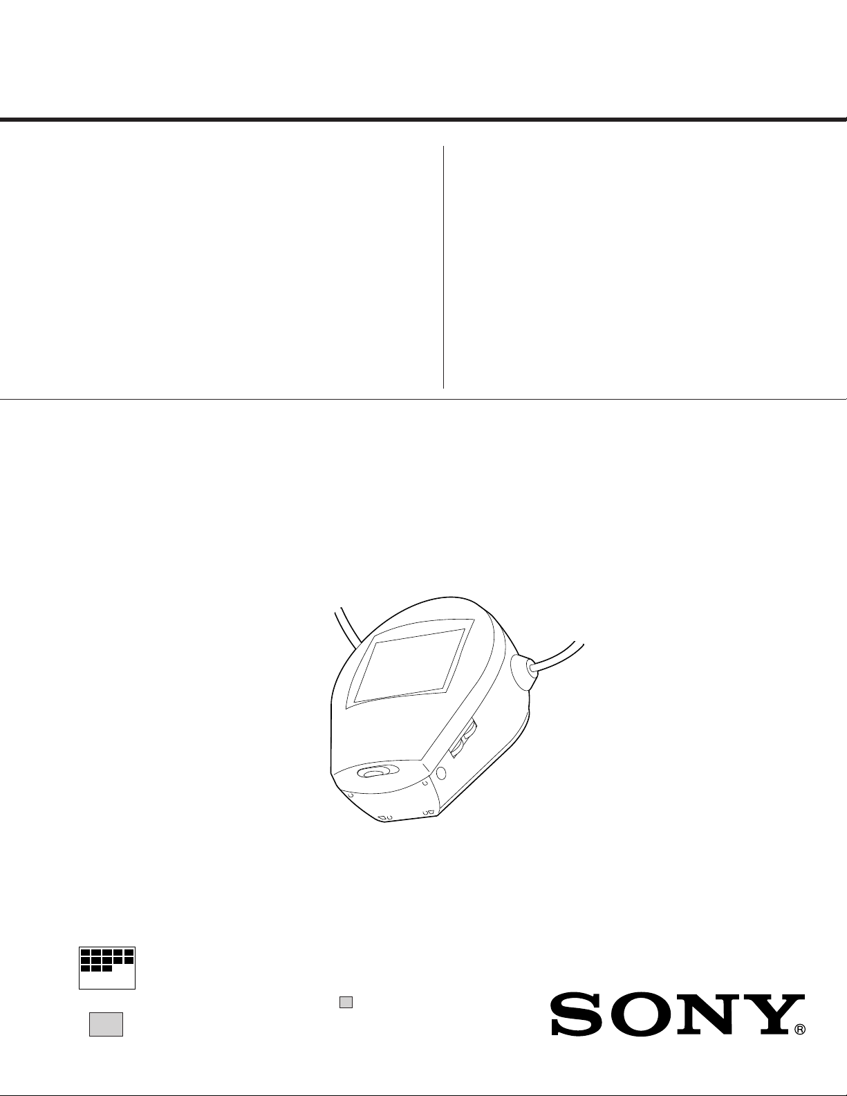
LCD COLOR TV
Page 2
FDL-PT222
SPECIFICATIONS TABLE OF CONTENTS
Section Title Page
1. GENERAL
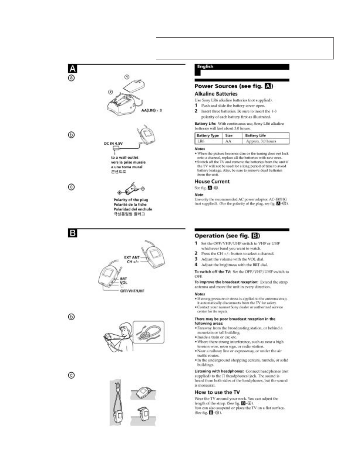
Power Sources (see fig. A) ...................................................... 3
Operation (see fig. B) .............................................................. 3
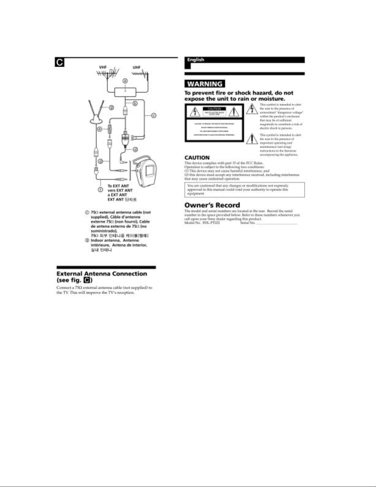
External Antenna Connection (see fig. C)............................... 4
WARNING .............................................................................. 4
2. DISASSEMBLY
2-1. Cabinets ........................................................................ 5
2-2. Service Position ............................................................ 6
3. CIRCUIT ADJUSTMENTS ............................................ 7
4. DIAGRAMS
4-1.Block Diagram (1)............................................................ 9
4-2.Block Diagram (2).......................................................... 11
4-3.Circuit Boards Location ................................................. 14
4-4.Printed Wiring Boards and Schematic Diagrams ........... 14
• T1 Board ..................................................................... 15
• A Board ....................................................................... 19
• B Board ....................................................................... 23
4-5.Semiconductors .............................................................. 27
5. EXPLODED VIEWS
5-1. Chassis Section .............................................................. 28
6. ELECTRICAL PARTS LIST........................................ 29
SHORT CIRCUIT THE ANODE OF THE PICTURE TUBE AND THE ANODE CAP TO THE METAL CHASSIS, CRT SHIELD, OR CARBON PAINTED ON THE CRT, AFTER REMOVING THE ANODE.
AN ISOLATION TRANSFORMER SHOULD BE USED DURING ANY SERVICE TO AVOID POSSIBLE SHOCK HAZARD, BECAUSE OF LIVE CHASSIS.
THE CHASSIS OF THIS RECElVER IS DIRECTLY CONNECTED TO THE
AC POWER LINE.
SAFETY-RELATED COMPONENT WARNING!!
COMPONENTS IDENTIFIED BY SHADING AND MARK ! ON THE SCHEMATIC DIAGRAMS, EXPLODED VIEWS AND IN THE PARTS LIST ARE
CRITICAL TO SAFE OPERATION. REPLACE THESECOMPONENTS
WITH SONY PARTS WHOSE PART NUMBERS APPEAR AS SHOWN IN
THIS MANUAL OR IN SUPPLEMENTS PUBLISHED BY SONY. CIRCUIT
ADJUSTMENTS THAT ARE CRITICAL TO SAFEOPERATION ARE IDENTIFIED IN THIS MANUAL. FOLLOW THESE PROCEDURES WHENEVER CRITICAL COMPONENTS ARE REPLACED OR IMPROPER OPERA-
TION IS SUSPECTED.
(CAUTION)
WARNING!!
– 2 –
Page 3
SECTION 1
GENERAL
The operating instructions mentioned here are partial abstracts from the
Operating Instructions Manual. The page numbers of the Operating
Instruction Manual remain as in the manual. (Part no : 4-083-376-11)
– 3 –
Page 4
– 4 –
Page 5
SECTION 2
DISASSEMBLY
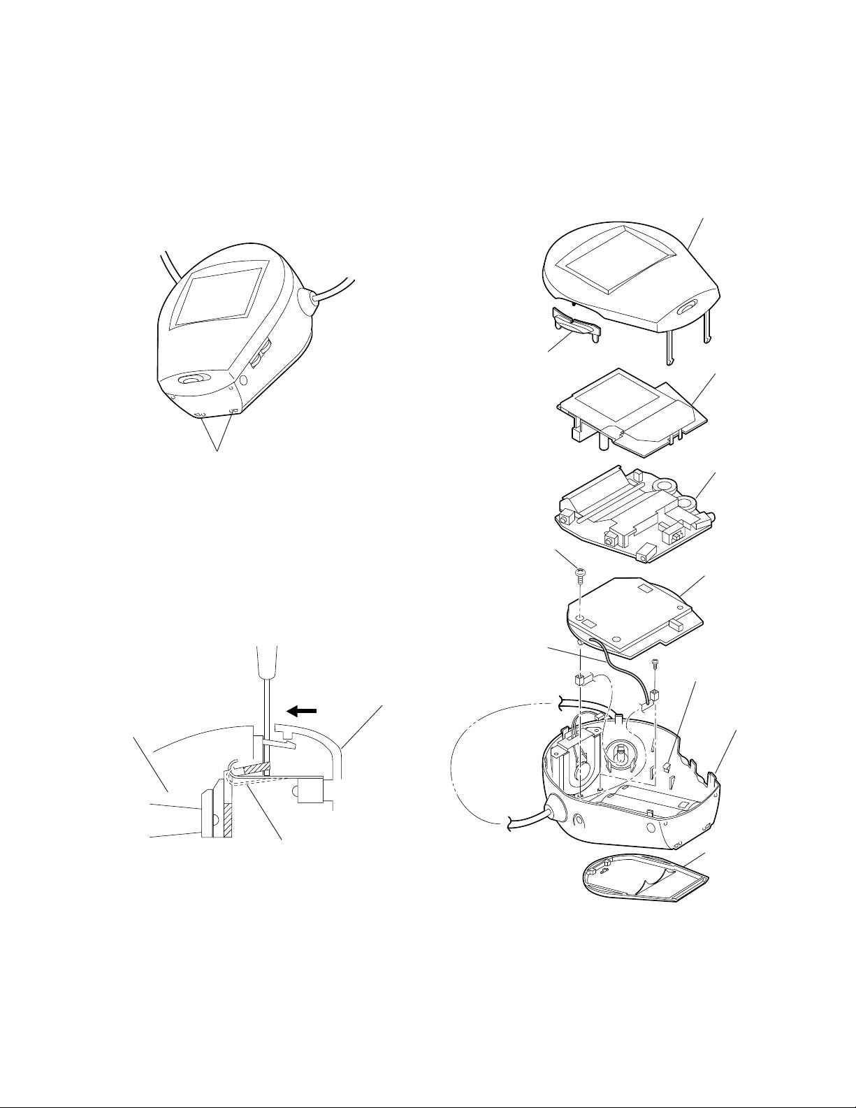
2-1. CABINETS
1. Remove the battery cover 8.
2. Push two claws with a screwdriver or equivalent on the bottom and
remove them.
FDL-PT222
1 front cabinet
2 channel button
3 B board
claw
3. While pushing the rear cabinet, remove claws of joints with
the front cabinet.
4. Insert a screwdriver or equivalent to the gap on the upper side of the
cabinet, and while pushing the lock spring, put it down to the rear cabinet
side.
5. Remove the channel button 2.
6. Disconnect CN501 (for speaker) on the A board.
7. Remove the B board 3 and the A board 4.
8. Remove solder for the lead wire (BLK) 9.
9. Remove a screw (+PTP2X6) 6 secured the T board 5.
10. Release the T1 board 5 from two claws (right and left) on the rear cabinet.
front cabinet
rear cabinet
lock spring
6 screw (+PTP2X6)
9 lead wire (BLK)
4 A board
5 T1 board
claw
7 rear cabinet
8 battery cover
– 5 –
Page 6
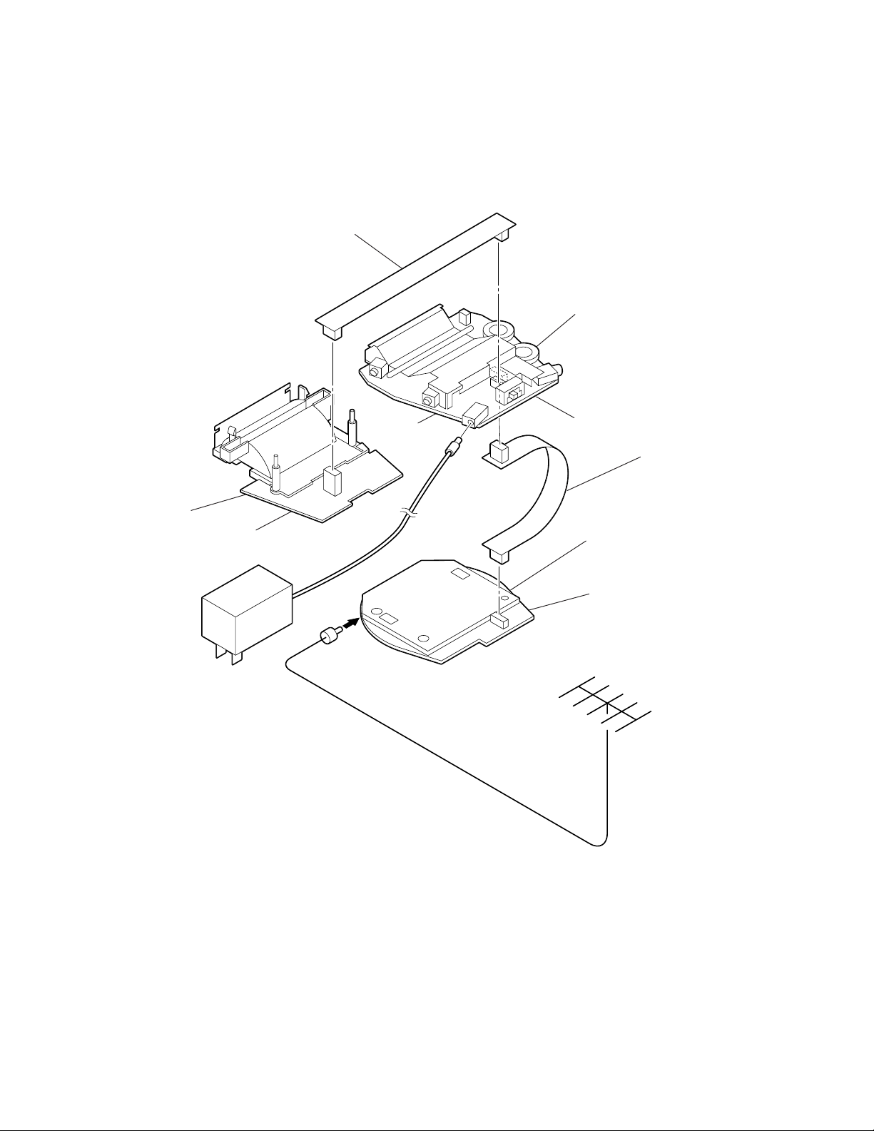
FDL-PT222
2-2. SERVICE POSITION
Cable for service
1-900-211-84
CN602
B board
CN301
AC power adaptor
J101
Mini-jack
CN601
A board
Cable for service
1-900-211-84
T1 board
CN201
Antenna
– 6 –
Page 7
SECTION 3
CIRCUIT ADJUSTMENTS
FDL-PT222
3-1.A BOARD ADJUSTMENT [+4.5V ALIGNMENT (RV601)]
Using a digital voltmeter measuring the voltage between
JL32 (+4.5V) and JL33 (GND). Adjust RV601 to obtain
the value shown below.
Standard Value = 4.45V± 0.05VDC
S601 position = UHF position
[+30.0V CHECK]
Check the voltage across JL29 (+30.0V) and JL33 (GND) .
Standard Value = 30.5V±1.5VDC
[AUDIO OUTPUT CHECK]
1. Feed the audio signal 1kHz 100% modulated.
2. Set RV501 to maximum.
3. Connect an oscilloscope between JL23 (SP) and JL15 (SP
GND).
4. Check the waveform on the oscilloscope becomes the standard value.
Standard Value = 1.5V-2.8Vp-p
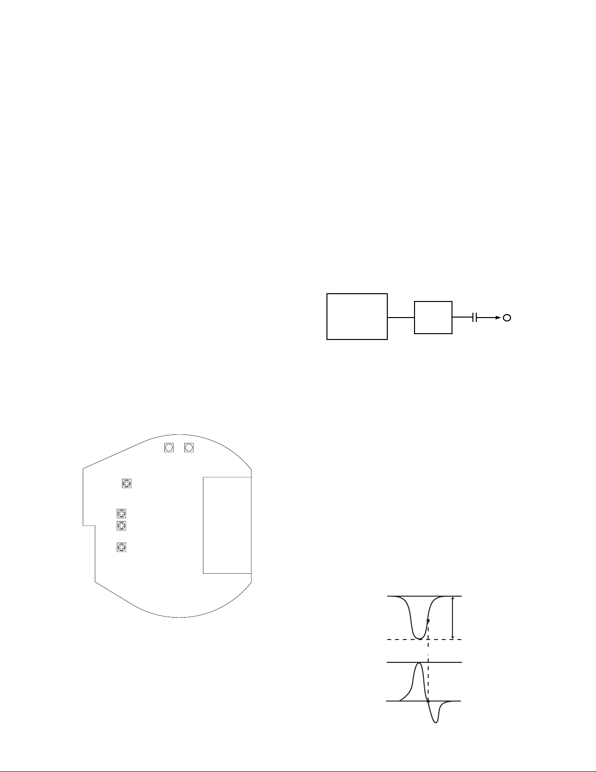
[VIF.AFT COARSE ADJUSTMNT (T201, T202)]
[SETUP]
1. Set S601 on the A board to VHF position.
2. Apply no signal to JL18 (RF).
3. Connect a 1 kΩ resistor between JL77 (+4.5V) and
JL28 (RF AGC).
4. Apply a sweep signal across JL26 (IF) and JL27(IF GND).
(Fig. 3-1)
Note : Set the sweep signal for JL26 to -30±5dBm. Keep the
distance to the ATT output JL26 as short as possible.
0.01µF
SWEEP
MARKER
GENERATOR
fo=45.75MHz±5kHz
ATT
JL26
75Ω 6dB
Fig. 3-1
3-2.T1 BOARD ADJUSTMENT
- T1 board - (Component side)
T201
T202
RV201
RV002
RV004
RV001
TU101
[ADJUSTMNT]
1. Connect an oscilloscope between JL72 (VIDEO) and JL71
(A.GND) and apply an external voltage (MGC) to JL26 to
obtain a waveform as shown in Fig. 3-2 (make sure not to
clip the extremely short portion).Adjust T202 so that the position at 45.75 MHz is the lowest point.
Note : Align JL51 (MGC) external voltage for approximately
a 1.0 Vp-p. Make sure that the JL51 (MGC) external
voltage does not exceed 4.3VDC.
2. Remove the external voltage (MGC) from JL51.
3. Connect an oscilloscope between JL31 (AFT) and JL30
(D.GND) and make a coarse adjustment of T201 so that wav eform is close to zero at the 45.75 MHz position.
4. Remove the 1 kilohm resistor connected between JL77 (+4.5V)
and JL28 (RF AGC).
1Vp-p
45.75MHz
– 7 –
0
Fig. 3-2
Page 8
FDL-PT222
[AFT FINE ADJUSTMENT(T201)]
1. Connect a 1 kilohm resistor between JL77 (+4.5V) and JL28
(RF AGC).
Note : Perform this adjustment as the last step in the
process since drift may occur due to aging.
2. Switch the sweep signal to CW.
fo= 45.75 MHz±5 kHz, -30±5dBm
Apply the abov e signal between JL26 (IF) and JL27 (IF GND)
and then make a fine adjustment of T201 so that the level be-
tween JL31 (AFT) and JL30 (D.GND) reaches2.2V±0.4VDC.
3. Remove the 1 kilohm resistor connected between JL77 (+4.5V)
and JL28 (RF AGC).
[RF. AGC ADJUSTMENT (RV201)]
1. Set S601 to VHF position and recei ve a VHF color bar signal
issued from a signal generator.
2. Adjust RV201 and align the screen for the optimal point so
that the snow noise disappears.
[CHANNEL DISPLAY POSITION ADJUSTMENT
(RV001, RV002, RV004)]
1. Set S601 to VHF position, a potentiometer (47kΩ±15kΩ)
across JL25(CS) and JL77 (+4.5 V) as sho wn in Fig. 2-6 and
short the points JL21(CH CAL) and JL30 (D.GND).
2. Receive channel 2 and align the channel display positions with
RV002(VP).
3. Receive channel 13 and align the display bar with R V004(VA).
4. Align while performing tracking to mutual interference in the
above steps 2 and 3.
5. Receive channels 3 & 4 and confirm that the display bar is
within the standards.
6. Set S601 to UHF.
7. Receive channel 14 and align the display position with
RV001(UP).
8. Receive channel 69 and confirm that the display bar is within
the standards.
Once again receive channel 14 and confirm that the display
bar is within the standards.
Note : Use caution since shifting channel 69 will also
cause channel 14 to shift.
9. Remove the potentiometer (47kΩ+15kΩ) you connected between JL25(CS) and JL77(+4.5V). Also remov e the short you
connected between points JL21 (CH CAL)and JL30(D.GND).
JL25 (CS)
JL77(+4.5V)
Display bar
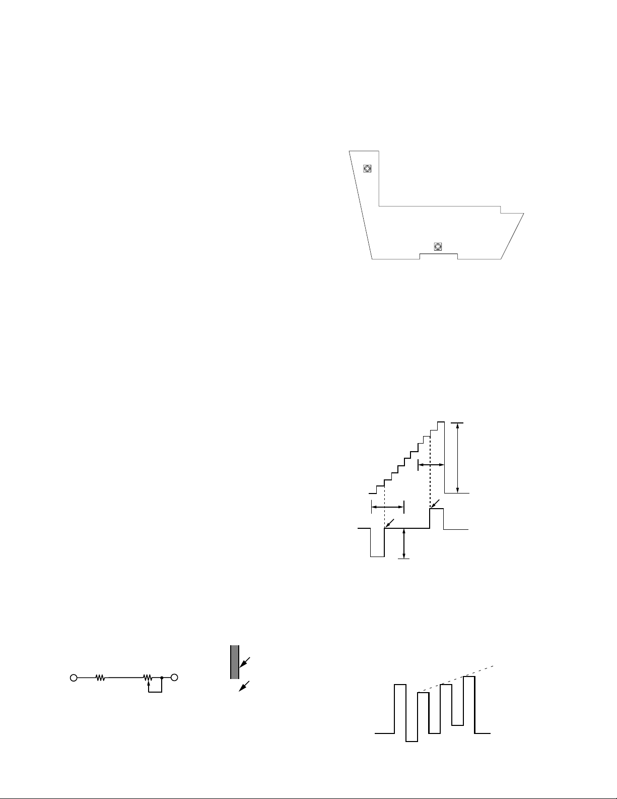
3-3.B BOARD ADJUSTMENT
- B board (Component side)
RV301
RV402
[CONTRAST ADJUSTMENT (RV402)]
1. Receive the stepped waveform signal in 10 steps.
2. Observe the waveform across JL83(G) and JL67(GND).
3. Check the contrast changes by turning RV402.
4. Connect an oscilloscope between JL84 (AUTO CB) and JL67
(D. GND) and adjust R V402 so that the v oltage of A portion
becomes 2.2+-0.2V.
5. Check the waveform as shown in Fig. 3-5.
6. At the same time, check the points C and D are within the
period as shown in Fig. 3-5.
100 IRE
JL83
0 IRE
JL84
C
A=2.2
±
Fig. 3-5
[COLOR PHASE (TINT) ADJUSTMENT (RV301)]
1. Receive the color bar signal from the signal generator.
2. Observe the waveform across JL81(B) and JL67(D.GND).
3. Adjust RV301 (TINT) so that the waveform level becomes as
shown in Fig. 3-6.
Contrast changes
D
0.2VDC
15kΩ
Fig. 3-3
Channel No.
6
VR(47kΩ)
*Channel No. and display
bar are to be in line.
Fig. 3-4
Fig. 3-6
– 8 –
Page 9

4-1. BLOCK DIAGRAM (1)
SECTION 4
DIAGRAMS
STRAP
ANTENNA
J101
EXT ANT
TU101
TUNER
ANT
AGC
IF
UB
HB
LB
MB
BALUN
T101
+4.5V
CN201
UB12
2
VHF
3
H.P
IC201 VIF/SIF DET
IF
IF
RF AGC
INV.
Q205
CF202
AFT
6
7
3
4RV201
14
15
16
23
17
21
IF
IF
AGC OUT
AGC DL
E-VDL
FM DET
LIM
SYNC
AFT
AFT COIL
IF AMP
AGC IF
FM
DET
SYNC
SEP
AFT
DET
AMP
REF COIL
REF COIL
AUDIO
SIF
DET OUT
SYNC SEP
VIDEO
BUFFER
LIMITER 10
VIDEO
LLD
19
20
13
AUDIO
AUDIO
5
AUDIO
TO
A BOARD
CN502
CF203
AUDIO
VIDEO
CF201
BUFFER
Q202
18
22
9
VIDEO
IF
IF AMP
Q201
IF
FILTER
SWF201
IC001
SWITCH
Q010-012
TUNER CONTROOL
BS
28
U/V
27
BS
COMPOSITION
BAND
SELECT
TUNING
CONTROL
BAND
SELECT
AUTO
RETURN
3
HP
COMPARATOR
DEFEAT
OUTPUT
SIGNAL
DEFECT
DEF
H SYNC
AFC
SUD
14
FH
1
4
5
6
FH SWITCH
Q005
Q007
AFC SWITCH
TU
CHANNEL DISPLAY
CHANNEL DISPLAY
POSITION CH1
CHANNEL DISPLAY
POSITION CH12
BUFFER
Q001
RV001
POSITION CH13
RV002
V LOW
RV004
V HI
AMP
Q002
7
H SYNC
BT
26
UP
18
UA
22
20
VLP
19
VHP
23
VHA
24
VLA
BT
GEN.
INITIAL
SET
BAR
DISPLAY
POSITION
ADJUST
CHARGE/
DISCHARGE
CIRCUIT
BAR
OUTPUT
8
CS
10
V
30
U
31
INV., SWITCH
Q003,004
IND
UP DOWN SW11
T1 (TUNER, VIF/SIF DET)
– 9 –
– 10 –
Page 10

4-2. BLOCK DIAGRAM (2)
TO
T1 BOARD
CN201
UB 12
VHF
H.P
AUDIO
VIDEO
CN502
2
3
5
9
AUDIO
+4.5V
RV501
VOL
S601
(1/2)
IC501 HEADPHONE AMP
3
2
VCC
IC401
MONITOR CONTROL
CN601 CN301
VHF
H.P
2
3
2
3
UHF
VHF
OFF
AUDIO
6
V+
7
AUDIO
J501
2
SPEAKER
VIDEOVIDEO
VIDEO
9
9
VIDEO
BUFFER
Q403
SYNC. SEP.
Q303
4037R2
34
HSO
V IN
CL2
CLB
CLA
BESTB
TPR1B
CP
D2
D3
D4
D1
DB 10
1
2
3
4
5
6
7
8
9
12
VM BUFFER
13TPR1
Q407
SWITCH
Q406
CL2
CL2
CLB
CLB
CLA
CLA
RES
RES
TPR2
TPR1
VSS
24
CP
40
CP
22
38
21
37
20
36
D2
12
D2
28
D3
11
D3
27
10
D4
26
D1
9
D1
25
13
29
2
6
VM
23
VM
39
VM
4
3
LCD
MONITOR
H SYNC
IND
UP DOWN SW 11
BATTERY
J701
DC IN 4.5V
7
8
S601
(2/2)
UHF
VHF
OFF
S001 S002
-
CH
D701
H SYNC
7
T601
9
RV601
+4.5V
RV450
PORT SWITCH
Q601-603
BUFFER
Q401
BRT
DRIVE
Q701
DRIVE
Q702
F601
+4.5V
+
8
4
+30V
T701
3
2
4
1
5
+30V
1
+4.5V
6
7
3
11 11BRT
8
6
IND
FR701
LCD
BACK LIGHT
7
88
IND SWITCH
Q408
IC301 Y/C JUNGLE
VIDEO IN
29
SYNC SEP
TINT CONT
19 10
RV301
TINT
3.58MHz
VCXO IN
21 11
VCXO OUT
23 12
X301
HD IN
CONTRAST
R OUT
G OUT
B OUT
51
INV.
Q302
35 H IN
38 INB
R40
AUTO CB
23
R IN
28
G IN
29
27
B IN
XT1
XTD
20
21
30TGL VL
BUFFER
Q402
X401
4.5MHz
RV402
CONTRAST
VDG
VDR
VDG
VDR
VDB
VDB
VS2
VS2
17
18
33
34
16
32
15
31
A (POWER SUPPLY, LCD BACK LIGHT, HEADPHONE AMP)
– 11 –
B (Y/C JUNGLE, MONITOR CONTROL)
– 12 –
Page 11

MEMO
G
D
S
B1 E1
C2
B2 C1
E2
2
3
4
5
6
7
8
9
0
!¡
!™
!¢
!§
!¶
!•
–
1
G
D
S
B2 E2
C1
B1 C2
E1
B2 E2
C1
B1 C2
E1
B2 E2
C1
B1 C2
E1
!ª
B1 E1
E2
C1(B2)
C2
@º
B1
E2
C1
C2
@™
@£
(B2)
E1
(B2)
E1
E2
B1
C2
C1
@¡
B1
E1
C2
B2
C1
E2
G
S
S
D
G
D
B1
E1
C2
B2
C1
E2
B1
E2
C2C1(B2)
E2
B1
C1
C2E1(B2)
C2
B1
C1
E2E1(B2)
C2
B1
C1
E2
B2
E1
C2
Ver.1.5
Transistor
(FET)
Transistor
Transistor
Transistor
Transistor
Transistor
Transistor
Transistor
Transistor
Transistor
Discrete semiconductot
(Chip semiconductors that are not actually used are included.)
Diode
Diode
Diode
Diode
Diode
Diode
Diode
Diode
Diode
Diode
Source
Source
Anode
Anode
(NC)
(NC)
Cathode
Anode
Cathode
Common
Cathode
Cathode
Common
Cathode
Cathode
Common
Common
Common
Common
Cathode
Anode
Base
Emitter
Collector
Base
Emitter
Collector
Drain
Gate
Gate
Drain
Device Printed symbol Terminal name
Circuit
Terminal name of semiconductors in silk screen
printed circuit (
*
)
Anode
Anode
Anode Cathode
Anode Anode
Cathode
!£
Transistor
(FET)
Transistor
(FET)
!∞
Emitter
Collector
Base
Transistor
Source
Gate
Drain
Cathode
Anode
Anode
Cathode
Anode
Anode
4-3. CIRCUIT BOARDS LOCATION
Note: The symbol display is on the component slde.
The components identified by shading and mark
are critical for safety. Replace only with part number
B
specified.
The symbol indicate fast operating fuse.
Replace only with fuse of same rating as maked.
T1
A
4-4. PRINTED WIRING BOARDS AND
SCHEMATIC DIAGRAMS
Note:
• Capacitors without voltage indication are all 50V.
• All resistors are in ohms.
kΩ=1000Ω, MΩ=1000kΩ
• Indication of resistance, which dose not have one for rating electrical power, is
as follows.
Pitch : 5mm
Rating electrical power :
•
•
•
•
: nonflammable resistor.
: fusible resistor.
: internal component.
: panel designation and adjustment for repair.
• All variable and adjustable resistors have characteristic curve B, unless otherwise
noted.
•
: earth-chassis.
• As to the voltage volue shown by the semiconductors on the Shematic Diagram,
see the another list
• Readings are taken with a color-bar signal input.
• Readings are taken with a 10MΩ digital multimeter.
• Voltages are dc with respect to ground unless otherwise noted.
• Voltage variations may be noted due to normal production tolerances.
• All voltages are in V.
• Circled numbers are waveform references.
•
•
: B+ bus.
: B– bus.
• : signal path.
Reference information
RESISTOR : RN MET AL FILM
: RC SOLID
: FPRD NONFLAMMABLE CARBON
: FUSE NONFLAMMABLE FUSIBLE
: RW NONFLAMMABLE WIREWOUND
: RS NONFLAMMABLE METAL OXIDE
: RB NONFLAMMABLE CEMENT
COIL : LF-8L MICRO INDUCTOR
:
CAP A CIT OR : T A T ANTALUM
: PS STYROL
: PP POLYPROPYLENE
: PT MYLAR
: MPS METALIZED POLYESTER
: MPP METALIZED POLYPROPYLENE
: ALB BIPOLAR
: ALT HIGH TEMPERATURE
: ALR HIGH RIPPLE
– 13 –
1
/
W
4
ADJUSTMENT RESISTOR
– 14 –
Page 12

T1 BOARD : IC001 AN5707NFAP
STOP DEF
13 14 15 17
CHCAL
L/H U/V
7 27 8
Vcc 5VBRT
AFC
H.P.
M.M.
H.syn
SUD
5
COMPARATOR
3
PLUSE WIDTH
2
SET
SIGNAL
DET
4
1
FH
DEFEAT
OUT
TUNING
CONTROL
UP
BSTOP
DN
INPUT
CONTROL
6
AUTO
INITIAL RESET
29
GND
RETURN
9
BT GENERATOR
26
16
32
25
26
BTNCNCNCNC
CHARGE/
DISCHAGE
12 11
10
C.S.
CHAMANU
T1 BOARD : IC201 M51348AFP
13AUDIO OUT
BUFFER
14E-VDL
LIMITER
15FM DET IN
FM DET
16LIMITER OUT
17AFT OUT
18VIDEO OUT
19REF COIL
20REF COIL
VIDEO
DET
VIDEO AMPAFT
2nd
Amp
1st
Amp
21AFT COIL
AGC
22SYNC SEP IN
23SYNC OUT
24
SYNC
SEP
IF AGC
DET
GND (SIF)
12
DC F/B
11
SIF IN
10
Vcc (SIF)
9
GND (VIF)
8
IF IN
7
IF IN
6
Vcc (VIF)
5
RF AGC DELAY
4
RF AGC OUT
3
AGC FILTER II
2
1IF AGC ADJ
AGC FILTER I
BAND
SW
BS ADD
BAR OUTPUT
BAR DISPLAY
POSITION
ADJUST
24
23
VHA VLA
28 BS
30 V OUT
31 U OUT
18 UP
20 VLP
19 VHP
21 CON
22 UA
G
• T1 BOARD WAVEFORMS
1
3.4Vp-p (H)
1
STRAP
ANTENNA
A
1
2
3 4
2
EXT ANT
T101
6
J101
TU101
G
ANT
IFMBLBHBUBTUAGC
R101
100
:CHIP
B
C105
C001
4.7
25V
:7L
DEF
STOP
CHCAL
IC001
AN5707NFAP
R001
100k
:CHIP
C002
6.3V
MANU
470p B:CHIP
47
:7L
C101
1/16V F:CHIP
R031
82k
:CHIP
Q004
UN2110-TX
9
10111213141516
CS
NC
CHA
VCC
UH
SUD
AFC
HSYNC
H.P
2
M.M
1 2 3 4 5 6 7 8
FH
V OUT
U OUT
NC
32
R011
10k
:CHIP
30V
MA152WK-TX
R022
27k
:CHIP
ULOW
RV001
47k
:CHIP
VLOW
RV002
47k
:CHIP
VHI
Q001
2SB709A-R
R008
270k
:RN-CP
1
2
4
1
4
3
6
D001
2
1
RV004
100k
:CHIP
5
3
30V
:RN-CP
2
4.5V
R012
330k
:CHIP
C011
10
16V
:7L
NC
BRT
1718192021222324
UP
C003
VHP
560p
CH:CHIP
VLP
CON
UA
R002
100k
VHA
:CHIP
VLA
R030
R003
0
68k
:CHIP
:CHIP
R023
:CHIP
R004
47k
:CHIP
1
4
6
3
5
R009
33k
R047
10k
:CHIP
0
2
Q002
XN4601
C012
F:CHIP
:CHIP
16V
R005
150k
1
NCBTU/VBSGND
25262728293031
C
D
E
F
Q010
XN1115
3
R046
47k
:CHIP
5
Q011
XN4215
Q012
XN2210
UN211D-TX
D002
R016
39k
:CHIP
C014
0.1 25V F:CHIP
C007
0.001 B:CHIP
R017
18k :CHIP
C008
0.47
25V
F:CHIP
2
43
Q007
Q003
UN2210-TX
MA157-TX
IF
R021
100k
:CHIP
B:CHIP
R013
56k :CHIP
C021
0.1
F:CHIP
F:CHIP
C004
47
6.3V
:7L
:CHIP
3.7Vp-p (H)
C016
0.1
25V
F:CHIP
R029
470
:CHIP
C005
0.01
R014
25V
39k
:CHIP
C006
0.1
25V
R010
2.2
:CHIP
R018
100k
4.5V
C210
0.01
B:CHIP
:CHIP
IF
2SC3837KT146Q
R216
1.2k
:CHIP
R218
68
R219
:CHIP
3
0.9Vp-p (H)
98765
R032
2.2k
:CHIP
C015
100p
AUDIO
CH:CHIP
R201
680
:CHIP
0.001
B:CHIP
680 :CHIP
:CHIP
10k :CHIP
131415161718192021222324
OUT
AUDIO
(SIF)
GND
C213
0.01
B:CHIP
C204
R208
R228
10k
VIDEO
Q202
2SB709A-R
SIF
:CHIP
1k
R221
4.5V
LLD
DELAY
0.01 B:CHIP
R241
180k
:CHIP
31
REF COIL
(VIF)
VCC
C215
47
6.3V
:7L
R202
220
:CHIP
CF201
TPS4.5MC
4
VIDEO
321 6
R209
1.8k :CHIP
DET OUT
REF COIL
IC201
M51348AFP
IF IN
IF IN
IF
IF
R224
1.5k
:CHIP
RV201
1k
:CHIP
R229
8.2k
:CHIP
R231
:FR-CP
L201
15µH
R205
R210
100k :CHIP
33k :CHIP
AFT OUT
GND
8
12
3
C203
0.1 25V F:CHIP
R212
(VIF)
C212
0.01 B:CHIP
:CHIP
680 :CHIP
LIMITER
VCC
SIF
R240
3
CF202
OUT
10k
(SIF)
C202
0.01
B:CHIP
VIDEO VIDEO
C205
21
R206
10
16V
1.8k :CHIP
:7L
CDA4.5MC
R213
C206
27p CH:CHIP
E-VDL
FM DETIN
SIF IN
DC F/B
109 11 12
21
3
CF203
C218
0.01
SFSL4.5MDB
B:CHIP
C234
0.01
B:CHIP
R242
C235
470
0.001
:CHIP
B:CHIP
T201 T202
45.75MHZ 45.75MHZ
T1
TUNER,
VIF, SIF DET
L205
Q201
0.82µH
:FR-CP
R234
C229
1.2k
0.01
:CHIP
B:CHIP
R220
390
47
:CHIP
:CHIP
R214
1k
B:CHIP
C209
0.01
C211
0.01
B:CHIP
R215
10
:CHIP
SWF201
F1248
I
132
SWF
GOO
4.5V
IF
:FR-CP
4
L206
R217
1µH
3.3k :CHIP
IF
4.5V
AFT
6
CH:CHIP
4.5V
R243
22k
:CHIP
ADJ
IF AGC
AGC
FILTER OUT
1 2 3 4 5 6 7
R235
5.6k
:CHIP
C222
10
16V
:7L
R226
R225
3.3k
4.7k
:CHIP
C223
:CHIP
1
C224
0.01
B:CHIP
C207
10p
SYNC OUT
AGC
:CHIP
C219
3.3
1
2
34
R223
SYNC SEP
OUT
FILTER IN
RF AGC
1k
C225
R230
:CHIP10:CHIP
AFT COIL
RF AGC
C226
0.01 B:CHIP
10
10
CN201
12P
1
D.GND
2
VHF
3
H.P
4
4.5V
5
AUDIO
6
30V
7
H.SYNC
8
IND
9
R233
:CHIP
VIDEO
10
A.GND
11
UP DOWN SW
12
UB
100
A.GND
C228
0.01
B:CHIP
C236
22
6.3V
:7L
Q203
UN2210
30V
B-¥SS10904.<U..>-T1.
TO
A BOARD
CN602
11
– 15 –
– 16 –
Page 13

1
A
B
C
D
E
2
98765
43
T1
[ ]
ELECTRONIC TUNRTR, VIF, SIF
T1 BOARD IC VOLTAGE LIST
Pin Volt Pin Volt Pin Volt
IC001 1 2.7
20
3 0.3
4 0.5
5 2.5
6 2.5
7 2.5
8 4.3
910 0.7
11 2.5
12 0
13 0.3
14 0.0
15 3.7
16 17 18 0
19 2.2
20 2.2
21 2.9
22 0.8
23 2.1
24 2.1
25 26 1.7
27 3.8
28 0
29 GND
30 0
31 0
32 0
IC201 1 3.4
2 3.4
3 1.6
4 3.3
5 4.2
6 3.4
7 3.4
8 GND
9 4.3
10 1.6
11 1.6
12 GND
13 1.8
14 3.5
15 2.1
16 1.5
17 2.4
18 2.0
19 1.9
20 1.9
21 3.4
22 3.4
23 0.4
24 1.7
T1 BOARD
DIODE
D001 B-7 8
D002 B-2 7
IC
IC001 C-2
IC201 B-6
TRANSISTOR
Q001 D-8 1
Q002 D-8 !•
Q003 B-8 1
Q004 B-8 1
Q007 B-2 2
Q010 D-10
Q011 D-7 !¶
Q012 D-7 1
Q201 D-6 2
Q202 B-3 1
Q203 D-4 1
VARIABLE
*
*
– T1 Board –
RESISTOR
RV001 B-3
RV002 B-3
RV004 B-3
RV201 B-3
T1 BOARD TRANSISTOR VOLTAGE LIST
BCE
Q003 0 3.7 GND
Q004 3.7 0.7 4.3
Q007 2.6 0.5 4.3
Q201 1.0 4.2 0.3
Q202 1.9 GND 2.6
Q203 0 3.5 GND
123456
Q002 0 1.7 2.2 29.5 1.7 2.2
< Component Side >
< Conductor Side >
– 17 –
– 18 –
Page 14

1
NC1NC 8
V+
2+INPUT 7
OUTPUT
100kΩ
50kΩ300Ω
3-INPUT
6
POWER
GND
4GND 5
BIAS
+
-
A BOARD : IC501 NJM2070M
2
43
98765
A
B
C
D
E
TO
T1 BOARD
CN201
DRY BATTERY
3PCS. 4.5V
CN602
12P
D.GND
VHF
H.P
4.5V
AUDIO
30V
H.SYNC
IND
VIDEO
A.GND
UP DOWN SW
UB
TO SPEAKER
2
J501
POWER SUPPLY,
A
LCD BACK LIGHT,
1
2
3
4
5
6
7
8
9
10
11
12
HEADPHONE AMP
AUDIO
VIDEO
CH -
S001
21
3
S002
CH +
21
3
R028
10k
:CHIP
C501
0.01
B:CHIP
UNREG
R617
UHF
68
:CHIP
VHF
S601
OFF
F601
1A
125V
VOL
30V
R509
120k
:CHIP
RV501
10k
R513
2.2
:CHIP
C506
0.1
25V
F:CHIP
1
3
2
Q601
2SD601A-R
C504
16V
:7L
B:CHIP
10
C503
0.01
C502
100
6.3V
:7L
1 2 3 4
R510
10k
:CHIP
30V
R601
47k
:CHIP
R608
47k
:CHIP
C602
F:CHIP 100p
UNREG
AUDIO
5678
R605
100 :CHIP
0.0047
B:CHIP
Q603
2SD1119-Q
C604R603R602
R604
330
:CHIP
C505
6.3V
C605
CH:CHIP
100
:7L
C507
0.22
F:CHIP
R501
4.7
:CHIP
R504
470
:CHIP
25V
R505
470
:CHIP
R506
390
:CHIP
R616
10k
:CHIP
T601
9
8
4
5
NC
NC
V+
+IN
OUTPAT
-IN
GND
GND
IC501
NJM2070M-TE2
VIDEO VIDEO
D605
1SS355TE
Q602
2SD601A-R
C601
C603
100 10V :7L
0.1
25V
B:CHIP
47k
0.1
:CHIP22:CHIP
25V
SB01-15CP
1
6
7
3
CH:CHIP
2
C610
220p
D602
R611
2.2k
:CHIP
SP
1
D603
SB05-05CP
B:CHIP
CN501
SP.GND
2
R610
100
:CHIP
C619
0.01
C611
2P
D406
MA157-TX
R450
100k
:CHIP
30V
Q401
UN2215
R451
82k
:CHIP
3
2
1
RV450
50k
BRT
VIDEO
CN601
12P
1
D.GND
2
VHF
3
H.P.
4
4.5V
5
D.GND
6
A.GND
7
H.SYNC
8
IND
9
VIDEO
10
A.GND
11
BRT
12
NC
TO
B BOARD
CN301
4.5V
R615
10k
:CHIP
10
:7L
C613
C612
220 16V :7L
0.01 B:CHIP
MA8360-TX
D604
C615
0.01 B:CHIP
C614
0.01 B:CHIP
Q610
2SB709A-R
D601
MA8043-M
R614
:CHIP
33k :CHIP
1
3
2
:CHIP
:FR-CP
R612
330
RV601
220
:CHIP
+4.5V
R613
560
L601
47µH
4.5V
C616
0.01
B:CHIP
C617
220
16V
:7L
– 19 –
F
G
H
DC IN 4.5V
B-¥SS10904.<U..>-A.. (02)
L701
100µH
R701
330
1/8W
:CHIP
Q701
2SC2873Y
C701
100
Q702
6.3V
:7L
2SC2873Y
D701
J701
1
+
3
2
-
11EQS04-TA1B
C702
0.22
2
3
9
C703
22p
T701
8
7
6
2kV
FR701
4
:PP
1
5
C704
0.1
25V
F:CHIP
– 20 –
Page 15

1
A
B
C
D
E
F
G
H
I
2
5
43
A
[ ]
AUDIO AMP, PC IN, BACK LIGHT
– A Board –
A BOARD
DIODE
D406 G-5 6
D601 G-4 3
D602 D-4 5
D603 G-4 4
D604 C-5 3
D605 C-4 3
D701 D-3 –
*
IC
IC501 G-5
TRANSISTOR
Q401 G-5 1
Q601 C-4 2
Q602 D-4 2
Q603 F-4 2
Q610 C-5 2
Q701 G-3 2
Q702 G-3 2
*
VARIABLE
RESISTOR
RV450 C-6
RV501 D-5
RV601 C-5
A BOARD IC VOLTAGE LIST
Pin Volt
IC501 1 -
20
3 0.6
4 GND
5 GND
6 1.3
7 3.4
8-
< Component Side >
A BOARD TRANSISTOR VOLTAGE LIST
BCE
Q401 13.9 30.5 13.4
Q601 0.5 1.2 GND
Q602 0.7 3.1 0.2
Q603 0.2 3.0 GND
Q610 30.7 0.5 30.7
Q701 0 3.0 GND
Q702 0 3.0 GND
– 21 –
< Conductor Side >
– 22 –
Page 16

2.0Vp-p (4.5MHz)
1
1.1Vp-p (4.43MHz)
2
1.0Vp-p (H)
3
0.7Vp-p (H)
4
4.1Vp-p (H)
5
1.4Vp-p (H)
6
1.4Vp-p (H)
7
1.4Vp-p (H)
8
• B BOARD WAVEFORMS
1
2
43
98765
10
11
A
4.5V
B
CN301
C
TO
A BOARD
CN601
D
E
F
G
12P
D.GND
VHF
H.P.
4.5V
D.GND
A.GND
H.SYNC
IND
VIDEO
A.GND
BRT
NC
1
2
3
4
5
6
7
8
9
10
11
12
R309
10
:CHIP
C301
47
6.3V
:7L
D303
MA8051
X301
3.58MHz
VIDEO
IC301
M52042FP
3
VIDEO
C307
4.7
25V
:7L
R311
150k
:CHIP
R320
1.5k
:CHIP
C314
4.7
25V
:7L
C313
0.0015
B:CHIP
Y/C JUNGLE,
B
MONITOR CONTROL
4.5V
R301
0
:CHIP
C303
C311
180p
0.01
B:CHIP
:CHIP
C302
15p
CH:CHIP
:CHIP
VCXO
2
VCC
VIDEOINSYNC
1 2 3 4 5 6 78109 11 12
4
R312
560
:CHIP
C308
680p
B:CHIP
R323
2.2M
:CHIP
R324
:CHIP
R303
470
VCXO
10k
OUT
SEP IN
VCXO
MONITER
ACC
FILTER
R313
3.3k :CHIP
R304
IN
VCXO
CONT
COLER
5
HD IN
SYNC
OUT
C309
470k :CHIP
Q303
2SB709A-R
1M :CHIP
R306
TINT
CONT
CLUMP
1SS355TE
R310
:CHIP
R314
0.1 25V B:CHIP
100k
:CHIP
C310
0.01
B:CHIP
D302
MA8051
D301
68k
RV301
47k
:CHIP
47k :CHIP
R305
FILTER
KILLER
CHROMA
TRAP
APC
Y OUT
C312
F:CHIP
C306
0.033
25V
B:CHIP
C304
0.1
25V
B:CHIP
SW
FILTER
CONTRAST
0.1
25V
OUT
KILLER
R OUT
R
131415161718192021222324
PIX
CONT
7
G OUT
G
:CHIP
:CHIP
B OUT
:CHIP
R307
GND
R315
B
R308
4.7k
22k
R403
47
:CHIP
R405
68k
:CHIP
1SS355TE
D405
C402
4.7
35V
:7L
47k
8
6
R318
39k
:RN-CP
R322
68k
:RN-CP
R
G
R316
270k
:CHIP
B
R317
4.7k
:CHIP
Q302
UN5210
CH:CHIP
C315
R431
33k
:CHIP
D401
1SS355TE
R416
47
:CHIP
47p
:CHIP
:CHIP
:CHIP
R406
R407
2.2k
R408
2.2k
680
2SD1819A-R
C403
22
6.3V
:7L
C415
100
6.3V
:7L
C418
F:CHIP
C419
B:CHIP
CH:CHIP
CH:CHIP
Q402
C405
22
6.3V
:7L
R404
100
:CHIP
0.1
25V
0.1
25V
C420
12p
C421
12p
C422
0.001
B:CHIP
0.001 B:CHIP
4.5V
R401
100
:CHIP
R402
C406
100
22
:CHIP
6.3V
:7L
C407
47
6.3V
:7L
R430
0
:CHIP
4.5V
12
13
14
15
16
17
18
19
20
21
22
R429
3.3k
:CHIP
C424 R423
R422
C425
4.7
25V
:7L
R418
1.5k
:CHIP
R419
10k :CHIP
1k :CHIP
X401
C423
4.5V
R420
4.5MHz
0.001 B:CHIP
RB401 RB402 RB403 RB404
TPR1B
2.2kx2
1/16W
TPR1
:CHIP
VDDC
CV3
CV2
CV1
PLLO
PLLO2
XTI
1
XTO
VSSC
23 24 25 26 27 28 29 30 31 32 33
10k :CHIP
C427
0.1
25V
F:CHIP
R409
68k
:CHIP
C409 C410
0.1
0.1
25V
25V
B:CHIP
B:CHIP
R410
39k
:CHIP
214321432143214
DB
D1D4D3
VDDB
BESTB
2.2kx2
2.2kx2
1/16W
1/16W
:CHIP
:CHIP
IC401
A71-2980
AUTOCB
AUTOC
VDDABTBIN
RIN
B
R
6.8k :CHIP
R428
:CHIP
RV402
C428
47k
0.01
:CHIP
B:CHIP
47k
XP4601
D2
GIN
G
Q406
3
CLA
CLB
CL2
2.2kx2
1/16W
:CHIP
TGLVLRBPALB
R424
2.7k :CHIP
C411
0.47
25V
F:CHIP
R411
1M
:CHIP
C412
0.47
25V
F:CHIP
C408
0.01
B:CHIP
D403
1SS355TE
VSSB
G2
R2
B2
INB
HSO
VS2
HIN
VIN
C432
0.001
B:CHIP
44
43
42
41
40
39
38
37
36
35
34
R417
4.7k
:CHIP
2.2kx2 1/16W :CHIP
4.5V
:CHIP
Q403
UN2215
R421
10k
:CHIP
:CHIP
R436
43
21
1234567891011
CP
SGD1B
MUTEB
VSSA
R427
10k
RB405
1k
D404
1SS355TE
Q408
UN5210
R413
22k
:CHIP
C413 R412
100p
CH:CHIP
C414 R415
100p
CH:CHIP
Q407
XP4601
22k
:CHIP
R414
:CHIP
22k
:CHIP
22k
4.5V
B-¥SS10904.<U..>-B.. (02)
FP401
1
N.C.
2
TPR2
3
VSS
4
VM
5
VDD
6
TPR1
7
N.C.
8
N.C.
9
D1
10
D4
11
D3
12
D2
13
RESTB
14
VS1
15
VS2
16
VDB
17
VDG
18
VDR
19
VD1
20
CLA
21
CLB
22
CL2
23
VM
24
CP
25
D1
26
D4
27
D3
28
D2
29
RESTB
30
VS1
31
VS2
32
VDB
33
VDG
34
VDR
35
VD1
36
CLA
37
CLB
38
CL2
39
VM
40
CP
41
N.C.
42
N.C.
43
N.C.
TO
LCD UNIT
– 23 –
– 24 –
Page 17

1
A
B
C
D
E
F
G
2
5
43
B
[ ]
CHROMA, LCD INTERFACE
– B Board –
B BOARD IC VOLTAGE LIST
Pin Volt Pin Volt Pin Volt
IC301 1 3.0
2 3.1
3 0.6
45 3.5
6 2.5
78-
9 2.8
10 3.0
11 2.9
12 3.1
13 GND
14 0.3
15 16 17 1.5
18 3.7
19 1.6
20 2.0
21 3.4
22 23 2.0
24 4.2
IC401 1 1.3
20
3 0.8
4 0.8
5 2.7
6 2.7
7 2.8
8 2.8
9 3.3
10 1.9
11 3.9
12 3.9
13 0
14 3.9
15 1.7
16 1.7
17 1.7
18 1.7
19 1.7
20 2.0
21 2.0
22 GND
23 3.4
24 25 3.8
26 3.3
27 0.9
28 0.9
29 0.9
30 0.8
31 0.3
32 3.8
33 GND
34 1.8
35 1.1
36 0
37 0.3
38 3.6
39 GND
40 0
41 2.1
42 0
43 3.5
44 GND
B BOARD
DIODE
D301 B-2 3
D302 B-2 3
D303 F-2 3
D401 C-3 3
D403 F-4 3
D404 F-4 3
D405 B-3 3
IC
IC301 C-3
IC401 C-4
TRANSISTOR
Q302 C-3 2
Q303 B-2 2
Q402 B-3 2
Q403 C-3 2
Q406 C-5 @º
Q407 B-5 @º
Q408 C-3 2
VARIABLE
RESISTOR
RV301 B-2
RV402 C-4
*
*
< Component Side >
B BOARD TRANSISTOR VOLTAGE LIST
BCE
Q302 0.3 3.5 GND
Q303 3.6 1.8 4.1
Q402 3.9 4.4 3.2
Q403 2.1 0 GND
Q408 0 3.8 GND
123456
Q406 GND -0.7 6.5 12.4 13.3 6.5
Q407 1.8 0 6.5 1.8 1.8 13.3
– 25 –
< Conductor Side >
– 26 –
Page 18

4-5. SEMICONDUCTORS
3
4
4
3
A
A
16
1
2
3
5
4
9
6
7
8
11
24
21
22
25
23
18
17
19
19
20
15
14
13
12
A71-2980
1
TOP VIEW
44 pin QFP
XN4601
1
2
1
SECTION 5
EXPLODED VIEW
NOTE:
• Items with no part number and no
description are not stocked because they
SB-01-15CP
SB05-05CP
6
5
3
are seldom required for routine service
• The construction parts of an assembled part
are indicated with a collation number in the
remark column.
5-1. CHASSIS SECTION
2
6
3
2
5
4
3
1
3
2
1
r : 7-685-104-19 +P 2x6
• Items marked " * " are not stocked since
they are seldom required for routine
service. Some delay should be anticipated
when ordering these items.
The components identified by shading and
mark
are critial for safety.
!
Replace only with part number specified.
AN5707NFAP
1
TOP VIEW
32 pin QFP
M51348AFP
M52042FP
1
TOP VIEW
24 pin SOP
NJM2070M
827365
14
8 pin SOP
UN2110
UN211D
UN2210
UN2215
UN5210
2SB709A
2SC3837KQ
2SD601A
B
E
XN4215
MA8043
XP4601
MA8051
MA8240
MA8360
1SS355
ANODE
CATHODE
11EQS04
1
2
3
1
2
2SC2873Y
6
5
6
5
4
3
2SD1119-Q
CATHODE
B
C
E
ANODE
2SD1819A
3
C
2
E
1
B
MA152WK
3
2
1
MA157
2
1
3
2
1
2
1
C
REF. NO. PART NO. DESCRIPTION REMARK
–––––––– ––––––––– ––––––––––––– –––––––––
1 4-561-075-51 CABINET, FRONT
2 4-561-076-01 SWITCH, POWER
3 4-561-093-03 BUTTON, CHANNEL
4 4-561-090-01 SHIELD, PANEL
5 1-803-293-11 MODULE, INDICATOR (NTSC)
6 * 4-048-325-01 ILLUMINATOR
7 * A-1136-215-AB BOARD, COMPLETE
8 1-517-702-11 LIGHT, BACK
9 * 3-703-044-26 LABEL, CAUTION
11 * A-1299-522-AA BOARD, COMPLETE
12 4-561-096-01 INSULATING SHEET
13 4-561-091-01 SHIELD, TU
REF. NO. PART NO. DESCRIPTION REMARK
–––––––– ––––––––– ––––––––––––– –––––––––
14 4-561-097-01 INSULATING SHEET (2)
15 ! 1-693-467-11 TUNER UNITPLETE
16 * A-1395-039-AT1 BOARD, COMPLETE
17 4-561-081-01 SPRING (C), BATTERY
18 4-561-080-01 SPRING (B), BATTERY
19 4-561-079-01 SPRING (A), BATTERY
20 4-561-078-02 CASE, BATTERY
21 1-504-847-11 SPEAKER (2.8cm)
22 4-561-130-01 PLATE, LOCK
23 4-561-077-01 CABINET, REAR
24 1-754-205-11 ANTENNA, STRAP
– 27 –
– 28 –
Page 19

SECTION 6
ELECTRICAL PARTS LIST
FDL-PT222
T1
• Items marked " * " are not stocked since they are
The components identified by shading and
are critial for safety.
mark
!
Replace only with part number specified.
When indicating parts by reference number,
please include the board name.
REF. NO. PART NO. DESCRIPTION REMARK
–––––––– ––––––––– ––––––––––––– –––––––––
* A-1395-039-AT1 BOARD, COMPLETE
*********************
4-561-091-01 SHIELD, TU
4-561-096-01 INSULATING SHEET
4-561-097-01 INSULATING SHEET (2)
<CAPACITOR>
C001 1-126-794-11 ELECT 4.7µF 20% 25V
C002 1-126-513-11 ELECT 47µF 20% 6.3V
C003 1-163-135-00 CERAMIC CHIP 560pF 5% 50V
C004 1-126-513-11 ELECT 47µF 20% 6.3V
C005 1-163-021-91 CERAMIC CHIP 0.01µF 10% 50V
C006 1-163-038-91 CERAMIC CHIP 0.1µF 25V
C007 1-163-009-91 CERAMIC CHIP 0.001µF 10% 50V
C008 1-164-005-11 CERAMIC CHIP 0.47µF 25V
C011 1-126-791-11 ELECT 10µF 20% 16V
C012 1-164-346-11 CERAMIC CHIP 1µF 16V
C014 1-163-038-91 CERAMIC CHIP 0.1µF 25V
C015 1-163-251-11 CERAMIC CHIP 100pF 5% 50V
C016 1-163-038-91 CERAMIC CHIP 0.1µF 25V
C021 1-163-038-91 CERAMIC CHIP 0.1µF 25V
C101 1-164-346-11 CERAMIC CHIP 1µF 16V
C105 1-163-005-91 CERAMIC CHIP 470pF 10% 50V
C202 1-163-021-91 CERAMIC CHIP 0.01µF 10% 50V
C203 1-163-038-91 CERAMIC CHIP 0.1µF 25V
C204 1-163-009-91 CERAMIC CHIP 0.001µF 10% 50V
C205 1-126-791-11 ELECT 10µF 20% 16V
C206 1-163-237-11 CERAMIC CHIP 27pF 5% 50V
C207 1-163-227-11 CERAMIC CHIP 10pF 0.50pF 50V
C209 1-163-021-91 CERAMIC CHIP 0.01µF 10% 50V
C210 1-163-021-91 CERAMIC CHIP 0.01µF 10% 50V
C211 1-163-021-91 CERAMIC CHIP 0.01µF 10% 50V
C212 1-163-021-91 CERAMIC CHIP 0.01µF 10% 50V
C213 1-163-021-91 CERAMIC CHIP 0.01µF 10% 50V
C215 1-126-513-11 ELECT 47µF 20% 6.3V
C218 1-163-021-91 CERAMIC CHIP 0.01µF 10% 50V
C219 1-115-873-11 ELECT 3.3µF 20% 50V
C222 1-126-791-11 ELECT 10µF 20% 16V
C223 1-115-871-11 ELECT 1µF 20% 50V
C224 1-163-021-91 CERAMIC CHIP 0.01µF 10% 50V
C225 1-163-021-91 CERAMIC CHIP 0.01µF 10% 50V
C226 1-163-021-91 CERAMIC CHIP 0.01µF 10% 50V
C228 1-163-021-91 CERAMIC CHIP 0.01µF 10% 50V
C229 1-163-021-91 CERAMIC CHIP 0.01µF 10% 50V
C234 1-163-021-91 CERAMIC CHIP 0.01µF 10% 50V
C235 1-163-009-91 CERAMIC CHIP 0.001µF 10% 50V
C236 1-126-514-11 ELECT 22µF 20% 6.3V
seldom required for routine service. Some delay
should be anticipated when ordering these
items.
• All variable and adjustable resistors have
characteristic curve B, unless otherwise noted.
RESISTORS
• All resistors are in ohms
• F : nonflammable
• CAPACITORS
PF : µµ F
• There are some cases the reference
number on one board overlaps on the
other board. Therefore, when ordering
parts by the reference number, please
include the board name.
REF. NO. PART NO. DESCRIPTION REMARK
–––––––– ––––––––– ––––––––––––– –––––––––
<FILTER>
CF201 1-527-943-00 CERAMIC TRAP
CF202 1-760-642-11 DISCRIMINATOR, CERAMIC
CF203 1-577-559-21 FILTER, CERAMIC
<CONNECTOR>
CN201 1-785-361-11 CONNECTOR, BOARD T O BOARD
<DIODE>
D001 8-719-801-78 DIODE MA152WK-TX
D002 8-719-800-76 DIODE MA157-TX
<IC>
IC001 8-759-332-43 IC AN5707NFAP
IC201 8-759-176-91 IC M51348AFP-E1
<JACK>
J101 1-568-027-21 JACK, SMALL TYPE (EXT ANT)
<COIL>
L201 1-412-953-11 INDUCTOR 15µH
L205 1-412-938-11 INDUCTOR 0.82µH
L206 1-412-939-11 INDUCTOR 1µH
<TRANSISTOR>
Q001 8-729-216-22 TRANSISTOR 2SB709A-R-TX
Q002 8-729-402-84 TRANSISTOR XN4601-TW
Q003 8-729-424-76 TRANSISTOR UN2210-TX
Q004 8-729-424-38 TRANSISTOR UN2110-TX
Q007 8-729-424-45 TRANSISTOR UN211D-TX
Q010 8-729-403-45 TRANSISTOR XN1115-TX
Q011 8-729-422-54 TRANSISTOR XN4215-TW
Q012 8-729-424-76 TRANSISTOR UN2210-TX
Q201 8-729-031-37 TRANSISTOR 2SC3837KT146Q
Q202 8-729-216-22 TRANSISTOR 2SB709A-R-TX
– 29 –
Page 20

FDL-PT222
T1
B
The components identified by
shading and mark
cal for safety.
Replace only with part number
specified.
! are criti-
REF. NO. PART NO. DESCRIPTION REMARK
–––––––– ––––––––– ––––––––––––– –––––––––
Q203 8-729-424-76 TRANSISTOR UN2210-TX
<RESISTOR>
R001 1-216-097-11 RES-CHIP 100K 5% 1/10W
R002 1-216-097-11 RES-CHIP 100K 5% 1/10W
R003 1-216-093-91 RES-CHIP 68K 5% 1/10W
R004 1-216-089-91 RES-CHIP 47K 5% 1/10W
R005 1-216-101-00 RES-CHIP 150K 5% 1/10W
R008 1-218-762-11 METAL CHIP 270K 0.5% 1/10W
R009 1-216-687-11 METAL CHIP 33K 0.5% 1/10W
R010 1-216-298-00 RES-CHIP 2.2 5% 1/10W
R011 1-216-073-91 RES-CHIP 10K 5% 1/10W
R012 1-216-109-00 RES-CHIP 330K 5% 1/10W
R013 1-216-091-00 RES-CHIP 56K 5% 1/10W
R014 1-216-689-11 RES-CHIP 39K 5% 1/10W
R016 1-216-689-11 RES-CHIP 39K 5% 1/10W
R017 1-216-079-00 RES-CHIP 18K 5% 1/10W
R018 1-216-097-11 RES-CHIP 100K 5% 1/10W
R021 1-216-097-11 RES-CHIP 100K 5% 1/10W
R022 1-216-083-00 RES-CHIP 27K 5% 1/10W
R023 1-216-295-91 SHORT 0
R029 1-216-041-00 RES-CHIP 470 5% 1/10W
R030 1-216-295-91 SHORT 0
R031 1-216-095-00 RES-CHIP 82K 5% 1/10W
R032 1-216-057-00 RES-CHIP 2.2K 5% 1/10W
R046 1-216-089-91 RES-CHIP 47K 5% 1/10W
R047 1-216-073-91 RES-CHIP 10K 5% 1/10W
R101 1-216-025-11 RES-CHIP 100 5% 1/10W
REF. NO. PART NO. DESCRIPTION REMARK
–––––––– ––––––––– ––––––––––––– –––––––––
R235 1-216-067-00 RES-CHIP 5.6K 5% 1/10W
R240 1-216-073-91 RES-CHIP 10K 5% 1/10W
R241 1-216-103-00 RES-CHIP 180K 5% 1/10W
R242 1-216-041-00 RES-CHIP 470 5% 1/10W
R243 1-216-081-00 RES-CHIP 22K 5% 1/10W
<VARIABLE RESISTOR>
R V001 1-223-588-11 RES, ADJ, CARBON 47K (CHANNEL
R V002 1-223-588-11 RES, ADJ, CARBON 47K (CHANNEL
R V004 1-223-589-11 RES, ADJ, CARBON 100K (CHANNEL
R V201 1-223-583-11 RES, ADJ, CARBON 1K (RF AGC)
<SA W FILTER>
SWF201 1-767-766-12 FILTER, SAW
<TRANSFORMER>
T101 1-437-418-21 TRANSFORMER, BALUN
T201 1-411-278-11 COIL
T202 1-411-278-11 COIL
<TUNER>
TU101! 1-693-467-11 TUNER UNIT
DISPLAY POSITION 13ch)
DISPLAY POSITION 1ch)
DISPLAY POSITION 12ch)
R201 1-216-045-00 RES-CHIP 680 5% 1/10W
R202 1-216-033-00 RES-CHIP 220 5% 1/10W
R205 1-216-097-11 RES-CHIP 100K 5% 1/10W
R206 1-216-055-00 RES-CHIP 1.8K 5% 1/10W
R208 1-216-045-00 RES-CHIP 680 5% 1/10W
R209 1-216-055-00 RES-CHIP 1.8K 5% 1/10W
R210 1-216-085-91 RES-CHIP 33K 5% 1/10W
R212 1-216-045-00 RES-CHIP 680 5% 1/10W
R213 1-216-073-91 RES-CHIP 10K 5% 1/10W
R214 1-216-049-11 RES-CHIP 1K 5% 1/10W
R215 1-216-001-00 RES-CHIP 10 5% 1/10W
R216 1-216-051-00 RES-CHIP 1.2K 5% 1/10W
R217 1-216-061-91 RES-CHIP 3.3K 5% 1/10W
R218 1-216-021-00 RES-CHIP 68 5% 1/10W
R219 1-216-039-00 RES-CHIP 390 5% 1/10W
R220 1-216-017-91 RES-CHIP 47 5% 1/10W
R221 1-216-049-11 RES-CHIP 1K 5% 1/10W
R223 1-216-049-11 RES-CHIP 1K 5% 1/10W
R224 1-216-053-00 RES-CHIP 1.5K 5% 1/10W
R225 1-216-065-91 RES-CHIP 4.7K 5% 1/10W
R226 1-216-061-91 RES-CHIP 3.3K 5% 1/10W
R228 1-216-073-91 RES-CHIP 10K 5% 1/10W
R229 1-216-071-00 RES-CHIP 8.2K 5% 1/10W
R230 1-216-001-00 RES-CHIP 10 5% 1/10W
R231 1-216-001-00 RES-CHIP 10 5% 1/10W
R233 1-216-025-11 RES-CHIP 100 5% 1/10W
R234 1-216-051-00 RES-CHIP 1.2K 5% 1/10W
*************************************************************************************************************
* A-1136-215-AB BOARD, COMPLETE
*********************
<CAPACITOR>
C301 1-126-513-11 ELECT 47µF 20% 6.3V
C302 1-163-231-11 CERAMIC CHIP 15pF 5% 50V
C303 1-163-257-11 CERAMIC CHIP 180pF 5% 50V
C304 1-164-004-11 CERAMIC CHIP 0.1µF 10% 25V
C306 1-163-989-11 CERAMIC CHIP 0.033µF 10% 25V
C307 1-126-794-11 ELECT 4.7µF 20% 25V
C308 1-163-007-11 CERAMIC CHIP 680pF 10% 50V
C309 1-164-004-11 CERAMIC CHIP 0.1µF 10% 25V
C310 1-163-021-91 CERAMIC CHIP 0.01µF 10% 50V
C311 1-163-021-91 CERAMIC CHIP 0.01µF 10% 50V
C312 1-163-038-91 CERAMIC CHIP 0.1µF 25V
C313 1-163-011-11 CERAMIC CHIP 0.0015µF 10% 50V
C314 1-126-794-11 ELECT 4.7µF 20% 25V
C402 1-115-866-11 ELECT 4.7µF 20% 35V
C403 1-126-514-11 ELECT 22µF 20% 6.3V
C405 1-126-514-11 ELECT 22µF 20% 6.3V
C406 1-126-514-11 ELECT 22µF 20% 6.3V
C407 1-126-513-11 ELECT 47µF 20% 6.3V
– 30 –
Page 21

FDL-PT222
B
REF. NO. PART NO. DESCRIPTION REMARK
–––––––– ––––––––– ––––––––––––– –––––––––
C408 1-163-021-91 CERAMIC CHIP 0.01µF 10% 50V
C409 1-164-004-11 CERAMIC CHIP 0.1µF 10% 25V
C410 1-164-004-11 CERAMIC CHIP 0.1µF 10% 25V
C411 1-164-005-11 CERAMIC CHIP 0.47µF 25V
C412 1-164-005-11 CERAMIC CHIP 0.47µF 25V
C413 1-163-251-11 CERAMIC CHIP 100pF 5% 50V
C414 1-163-251-11 CERAMIC CHIP 100pF 5% 50V
C415 1-126-382-11 ELECT 100µF 20% 6.3V
C418 1-163-038-91 CERAMIC CHIP 0.1µF 25V
C419 1-164-004-11 CERAMIC CHIP 0.1µF 10% 25V
C420 1-163-229-11 CERAMIC CHIP 12pF 5% 50V
C421 1-163-229-11 CERAMIC CHIP 12pF 5% 50V
C422 1-163-009-91 CERAMIC CHIP 0.001µF 10% 50V
C423 1-163-009-91 CERAMIC CHIP 0.001µF 10% 50V
C424 1-163-009-91 CERAMIC CHIP 0.001µF 10% 50V
C425 1-126-794-11 ELECT 4.7µF 20% 25V
C427 1-163-038-91 CERAMIC CHIP 0.1µF 25V
C428 1-163-021-91 CERAMIC CHIP 0.01µF 10% 50V
C432 1-163-009-91 CERAMIC CHIP 0.001µF 10% 50V
<CONNECTOR>
CN301 * 1-779-896-11 CONNECTOR, BOARD TO BOARD 12P
<DIODE>
D301 8-719-988-61 DIODE 1SS355TE-17
D302 8-719-422-37 DIODE MA8051-TX
D303 8-719-422-37 DIODE MA8051-TX
D401 8-719-988-61 DIODE 1SS355TE-17
D403 8-719-988-61 DIODE 1SS355TE-17
D404 8-719-988-61 DIODE 1SS355TE-17
D405 8-719-988-61 DIODE 1SS355TE-17
<IC>
IC301 8-759-332-41 IC M52042FP-600C
IC401 8-759-368-68 IC A71-2980
<TRANSISTOR>
Q302 8-729-420-44 TRANSISTOR UN5210-TX
Q303 8-729-216-22 TRANSISTOR 2SB709A-R-TX
Q402 8-729-402-32 TRANSISTOR 2SD1819A-R-TX
Q403 8-729-902-99 TRANSISTOR UN2215-QRS(TX)
Q406 8-729-427-74 TRANSISTOR XP4601-TXE
Q407 8-729-427-74 TRANSISTOR XP4601-TXE
Q408 8-729-420-44 TRANSISTOR UN5210-TX
REF. NO. PART NO. DESCRIPTION REMARK
–––––––– ––––––––– ––––––––––––– –––––––––
R307 1-216-089-91 RES-CHIP 47K 5% 1/10W
R308 1-216-073-91 RES-CHIP 10K 5% 1/10W
R309 1-216-001-00 RES-CHIP 10 5% 1/10W
R310 1-216-093-91 RES-CHIP 68K 5% 1/10W
R311 1-216-101-00 RES-CHIP 150K 5% 1/10W
R312 1-216-043-91 RES-CHIP 560 5% 1/10W
R313 1-216-113-00 RES-CHIP 470K 5% 1/10W
R314 1-216-097-11 RES-CHIP 100K 5% 1/10W
R315 1-216-081-00 RES-CHIP 22K 5% 1/10W
R316 1-216-107-00 RES-CHIP 270K 5% 1/10W
R317 1-216-065-91 RES-CHIP 4.7K 5% 1/10W
R318 1-216-689-11 METAL CHIP 39K 0.5%
R320 1-216-053-00 RES-CHIP 1.5K 5% 1/10W
R322 1-216-695-11 METAL CHIP 68K 0.5%
R323 1-216-129-00 RES-CHIP 2.2M 5% 1/10W
R324 1-216-073-91 RES-CHIP 10K 5% 1/10W
R401 1-216-025-11 RES-CHIP 100 5% 1/10W
R402 1-216-025-11 RES-CHIP 100 5% 1/10W
R403 1-216-017-91 RES-CHIP 47 5% 1/10W
R404 1-216-025-11 RES-CHIP 100 5% 1/10W
R405 1-216-093-91 RES-CHIP 68K 5% 1/10W
R406 1-216-045-00 RES-CHIP 680 5% 1/10W
R407 1-216-057-00 RES-CHIP 2.2K 5% 1/10W
R408 1-216-057-00 RES-CHIP 2.2K 5% 1/10W
R409 1-216-093-91 RES-CHIP 68K 5% 1/10W
R410 1-216-689-11 RES-CHIP 39K 5% 1/10W
R411 1-216-121-11 RES-CHIP 1M 5% 1/10W
R412 1-216-081-00 RES-CHIP 22K 5% 1/10W
R413 1-216-081-00 RES-CHIP 22K 5% 1/10W
R414 1-216-081-00 RES-CHIP 22K 5% 1/10W
R415 1-216-081-00 RES-CHIP 22K 5% 1/10W
R416 1-216-017-91 RES-CHIP 47 5% 1/10W
R417 1-216-065-91 RES-CHIP 4.7K 5% 1/10W
R418 1-216-053-00 RES-CHIP 1.5K 5% 1/10W
R419 1-216-073-91 RES-CHIP 10K 5% 1/10W
R420 1-216-049-11 RES-CHIP 1K 5% 1/10W
R421 1-216-073-91 RES-CHIP 10K 5% 1/10W
R422 1-216-073-91 RES-CHIP 10K 5% 1/10W
R423 1-216-069-00 RES-CHIP 6.8K 5% 1/10W
R424 1-216-059-00 RES-CHIP 2.7K 5% 1/10W
R427 1-216-049-11 RES-CHIP 1K 5% 1/10W
R428 1-216-089-91 RES-CHIP 47K 5% 1/10W
R429 1-216-061-91 RES-CHIP 3.3K 5% 1/10W
R430 1-216-295-91 SHORT 0
R431 1-216-085-91 RES-CHIP 33K 5% 1/10W
R436 1-216-073-91 RES-CHIP 10K 5% 1/10W
1/10W
1/10W
<RESISTOR>
R301 1-216-295-91 SHORT 0
R303 1-216-041-00 RES-CHIP 470 5% 1/10W
R304 1-216-061-91 RES-CHIP 3.3K 5% 1/10W
R305 1-216-089-91 RES-CHIP 47K 5% 1/10W
R306 1-216-121-11 RES-CHIP 1M 5% 1/10W
<NETWORK RESISTOR>
RB401 1-236-416-11 NETWORK, RES 2.2K
RB402 1-236-416-11 NETWORK, RES 2.2K
RB403 1-236-416-11 NETWORK, RES 2.2K
RB404 1-236-416-11 NETWORK, RES 2.2K
RB405 1-236-416-11 NETWORK, RES 2.2K
– 31 –
Page 22

FDL-PT222
A
The components identified by
shading and mark
cal for safety.
Replace only with part number
specified.
! are criti-
REF. NO. PART NO. DESCRIPTION REMARK
–––––––– ––––––––– ––––––––––––– –––––––––
<VARIABLE RESISTOR>
R V301 1-223-588-11 RES, ADJ, CARBON 47K (TINT)
R V402 1-223-588-11 RES, ADJ, CARBON 47K (CONTRAST)
<CRYSTAL>
X301 1-567-505-11 OSCILLAT OR, CRYSTAL 3.58MHz
X401 1-760-601-21 VIBRAT OR, CRYSTAL 4.5MHZ
*************************************************************************************************************
* A-1299-522-AA BOARD, COMPLETE
C501 1-163-021-91 CERAMIC CHIP 0.01µF 10% 50V
C502 1-126-382-11 ELECT 100µF 20% 6.3V
C503 1-163-017-00 CERAMIC CHIP 0.0047µF 10% 50V
C504 1-126-791-11 ELECT 10µF 20% 16V
C505 1-126-382-11 ELECT 100µF 20% 6.3V
*********************
<CAPACITOR>
REF. NO. PART NO. DESCRIPTION REMARK
–––––––– ––––––––– ––––––––––––– –––––––––
D603 8-719-938-75 DIODE SB05-05CP-TB
D604 8-719-018-15 DIODE MA8360-TX
D605 8-719-988-61 DIODE 1SS355TE-17
D701 8-719-210-21 DIODE 11EQS04-TA1B
<FUSE>
F601 ! 1-533-631-31 FUSE, MICRO 1A 125V
<IC>
IC501 8-759-046-84 IC NJM2070M-TE2
<JACK>
J501 1-563-282-11 JACK, SMALL TYPE ( 2)
J701 1-568-907-21 JACK, DC(POLARITY UNIFIED TYPE)
<COIL>
L601 1-412-031-11 INDUCTOR 47µH
L701 1-408-615-31 INDUCTOR 100µH
(DC IN 4.5V)
C506 1-163-038-91 CERAMIC CHIP 0.1µF 25V
C507 1-164-222-91 CERAMIC CHIP 0.22µF 25V
C601 1-126-382-11 ELECT 100µF 20% 10V
C602 1-163-038-91 CERAMIC CHIP 0.1µF 25V
C603 1-164-004-11 CERAMIC CHIP 0.1µF 10% 25V
C604 1-163-017-00 CERAMIC CHIP 0.0047µF 10% 50V
C605 1-163-251-11 CERAMIC CHIP 100pF 5% 50V
C610 1-163-259-91 CERAMIC CHIP 220pF 5% 50V
C611 1-126-795-11 ELECT 10µF 20% 50V
C612 1-163-021-91 CERAMIC CHIP 0.01µF 10% 50V
C613 1-128-499-11 ELECT 220µF 20% 16V
C614 1-163-021-91 CERAMIC CHIP 0.01µF 10% 50V
C615 1-163-021-91 CERAMIC CHIP 0.01µF 10% 50V
C616 1-163-021-91 CERAMIC CHIP 0.01µF 10% 50V
C617 1-128-499-11 ELECT 220µF 20% 16V
C619 1-163-021-91 CERAMIC CHIP 0.01µF 10% 50V
C701 1-126-382-11 ELECT 100µF 20% 6.3V
C702 1-136-169-00 FILM 0.22µF 5% 50V
C703 1-109-879-11 CERAMIC 22pF 5% 2KV
C704 1-163-038-91 CERAMIC CHIP 0.1µF 25V
<CONNECTOR>
CN501 1-568-951-11 PIN, CONNECTOR 2P
CN601 * 1-770-605-11 CONNECTOR, BOARD TO BOARD 12P
CN602 * 1-770-605-11 CONNECTOR, BOARD TO BOARD 12P
<TRANSISTOR>
Q401 8-729-902-99 TRANSISTOR UN2215-QRS(TX)
Q601 8-729-422-29 TRANSISTOR 2SD601A-R-TX
Q602 8-729-422-29 TRANSISTOR 2SD601A-R-TX
Q603 8-729-421-15 TRANSISTOR 2SD1119-Q-TX
Q610 8-729-216-22 TRANSISTOR 2SB709A-R-TX
Q701 8-729-807-51 TRANSISTOR 2SC2873Y-TE12L
Q702 8-729-807-51 TRANSISTOR 2SC2873Y-TE12L
<RESISTOR>
R028 1-216-073-91 RES-CHIP 10K 5% 1/10W
R450 1-216-097-11 RES-CHIP 100K 5% 1/10W
R451 1-216-095-00 RES-CHIP 82K 5% 1/10W
R501 1-216-308-00 RES-CHIP 4.7 5% 1/10W
R504 1-216-041-00 RES-CHIP 470 5% 1/10W
R505 1-216-041-00 RES-CHIP 470 5% 1/10W
R506 1-216-039-00 RES-CHIP 390 5% 1/10W
R509 1-216-099-00 RES-CHIP 120K 5% 1/10W
R510 1-216-073-91 RES-CHIP 10K 5% 1/10W
R513 1-216-298-00 RES-CHIP 2.2 5% 1/10W
R601 1-216-089-91 RES-CHIP 47K 5% 1/10W
R602 1-216-089-91 RES-CHIP 47K 5% 1/10W
R603 1-216-009-91 RES-CHIP 22 5% 1/10W
R604 1-216-037-00 RES-CHIP 330 5% 1/10W
R605 1-216-025-11 RES-CHIP 100 5% 1/10W
<DIODE>
D406 8-719-800-76 DIODE MA157-TX
D601 8-719-421-82 DIODE MA8043-M(TX)
D602 8-719-989-93 DIODE SB01-15CP-TB
R608 1-216-089-91 RES-CHIP 47K 5% 1/10W
R610 1-216-025-11 RES-CHIP 100 5% 1/10W
R611 1-216-057-00 RES-CHIP 2.2K 5% 1/10W
R612 1-216-037-00 RES-CHIP 330 5% 1/10W
R613 1-216-043-91 RES-CHIP 560 5% 1/10W
– 32 –
Page 23

The components identified by
shading and mark ! are critical for safety.
Replace only with part number
specified.
REF. NO. PART NO. DESCRIPTION REMARK
–––––––– ––––––––– ––––––––––––– –––––––––
R614 1-216-085-91 RES-CHIP 33K 5% 1/10W
R615 1-216-073-91 RES-CHIP 10K 5% 1/10W
R616 1-216-073-91 RES-CHIP 10K 5% 1/10W
R617 1-216-021-00 RES-CHIP 68 5% 1/10W
R701 1-216-186-00 RES-CHIP 330 5% 1/8W
<VARIABLE RESISTOR>
R V450 1-223-901-21 RES, VAR 50K (BRT)
R V501 1-223-900-21 RES, VAR 10K (VOL)
R V601 1-223-581-11 RES, ADJ, CARBON 220 (+4.5V)
<SWITCH>
S001 1-571-532-21 SWITCH, TACTIL (CH -)
S002 1-571-532-21 SWITCH, TACTIL (CH +)
S601 1-762-368-11 SWITCH, SLIDE (OFF/VHF/UHF)
FDL-PT222
A
<TRANSFORMER>
T601 ! 1-431-580-11 TRANSFORMER, DC-DC CONVERTER
T701 1-427-918-11 TRANSFORMER, CONVERTER
************************************************************************************************************
MISCELLANEOUS
*****************
1-504-847-11 SPEAKER (2.8cm)
1-517-702-11 LIGHT, BACK
1-754-205-11 ANTENNA, STRAP
1-803-293-11 MODULE, INDICATOR (NTSC)
************************************************************************************************************
ACCESSORIES
*************
4-083-376-11 MANUAL, INSTRUCTION
– 33 –
Page 24

FDL-PT222
9-965-300-01
Sony EMCS Corporation
Ichinomiya T ec.
Quality Assurance Division
– 34 –
English
2001DR02-1
©2001.4
 Loading...