

Page 1
DVMC-DA2
SERVICE MANUAL
SPECIFICATIONS
Power requirements
DC IN 6V jack accepts the AC-MZ60A AC power adapter
(supplied), AC 120 V, 60 Hz
Power consumption
AC 120 V, 60 Hz, 5.1 W (max., AC power adapter)
Operating temperature
10°C to 35°C (50°F to 95°F)
Operating humidity
40 % to 80 %
Storage temperature
–20°C to 60°C (–4°F to 140°F)
Storage humidity
20 % to 80 %
Dimensions (approx.)
124 × 44 × 90.5 mm (5 × 1
(w/h/d, excluding projections)
Mass (approx.)
300 g (10 oz) (unit only)
3
/4 × 35/8 inches)
US Model
Canadian Model
Input/output connector
S VIDEO IN: Mini DIN 4-pin (1)
S VIDEO OUT: Mini DIN 4-pin (1)
VIDEO IN: RCA pin (1)
VIDEO OUT: RCA pin (1)
AUDIO IN: RCA pin (2): L, R
AUDIO OUT: RCA pin (2): L, R
DV IN/OUT : 4-pin S100 (100 Mbps) (1)
LANC : Stereo mini-minijack (1)
Supplied accessories
AC power adapter (AC-MZ60A)
DV connecting cable
AV connecting cable
S VIDEO connecting cable
LANC connecting cable
Operating instructions
Warranty card
Important safeguard
9-928-146-11
Design and specifications are subject to change without
notice.
MEDIA CONVERTER
Page 2

TABLE OF CONTENTS
1. GENERAL·····························································1-1
2. BLOCK DIAGRAMS
2-1. OVERALL BLOCK DIAGRAM ····································2-1
2-2. POWER BLOCK DIAGRAM ········································2-3
3. PRINTED WIRING BOARDS AND SCHEMATIC
DIAGRAMS
• SWX-22 (SWITCH) SCHEMATIC DIAGRAM ········· 3-2
• SWX-22 (SWITCH) PRINTED WIRING BOARD ····3-3
• IFX-52 (MAIN : SIDE A)
PRINTED WIRING BOARD ······································3-5
• IFX-52 (MAIN : SIDE B)
PRINTED WIRING BOARD ······································3-7
• IFX-52 (J CORE) SCHEMATIC DIAGRAM·············· 3-9
• IFX-52 (VFD) SCHEMATIC DIAGRAM················· 3-11
• IFX-52 (MECH CON) SCHEMATIC DIAGRAM····3-13
• IFX-52 (HI) SCHEMATIC DIAGRAM·····················3-15
• IFX-52 (DC CON) SCHEMATIC DIAGRAM··········3-17
• IFX-52 (AMP) SCHEMATIC DIAGRAM ················3-19
• IFX-52 (AGC) SCHEMATIC DIAGRAM ················3-21
• IFX-52 (AUDIO) SCHEMATIC DIAGRAM ············3-23
• IFX-52 (JACK) SCHEMATIC DIAGRAM···············3-25
• IFX-52 (CN) SCHEMATIC DIAGRAM ···················3-26
4. ELECTRICAL ADJUSTMENT ··························4-1
5. REPAIR PARTS LIST
5-1. EXPLODED VIEWS ······················································5-1
5-2. ELECTRICAL P ARTS LIST ··········································5-2
SAFETY-RELATED COMPONENT WARNING!!
COMPONENTS IDENTIFIED BY MARK 0 OR DOTTED LINE WITH
MARK 0 ON THE SCHEMATIC DIAGRAMS AND IN THE PARTS
LIST ARE CRITICAL TO SAFE OPERATION. REPLACE THESE
COMPONENTS WITH SONY PARTS WHOSE PART NUMBERS
APPEAR AS SHOWN IN THIS MANUAL OR IN SUPPLEMENTS
PUBLISHED BY SONY.
ATTENTION AU COMPOSANT AYANT RAPPORT
À LA SÉCURITÉ!
LES COMPOSANTS IDENTIFÉS P AR UNE MARQUE 0 SUR LES
DIAGRAMMES SCHÉMA TIQUES ET LA LISTE DES PIÈCES SONT
CRITIQUES POUR LA SÉCURITÉ DE FONCTIONNEMENT. NE
REMPLACER CES COMPOSANTS QUE PAR DES PIÈSES SONY
DONT LES NUMÉROS SONT DONNÉS DANS CE MANUEL OU
DANS LES SUPPÉMENTS PUBLIÉS PAR SONY.
— 2 —
Page 3
Overview
5
-US
Capturing images from an analog video unit using a PC
(page 13-15)
You can capture images from an analog video unit connected to your
PC via the media converter using the DV (i.LINK) connector.
You can operate the analog video unit from the PC by connecting to the
LANC (Local Application Control Bus System) connectors of the media
converter and the analog video unit. (Compatible software is required
for respective operations in the PC.)
In this case, you can edit a movie or add titles using your PC. You can
also print out the captured images using your PC printer instead of a
video printer.
Selecting the audio mode when recording to the DV unit
(page 9)
You can add messages or background music after recording.
When you record to the DV unit from an analog video unit, you can
select 16-bit audio mode for higher quality, or 12-bit audio mode for
adding messages or background music (post sound recording).
Listening to the audio with the desired mixing rate (page 12)
When playing back video recorded in 12-bit audio mode on a DV unit
via the media converter, you can listen to: the recorded message and/or
background music only (post sound recording), the original audio, or
the combined audio of both tracks with the desired mixing rate (5
steps).
Original sound
+
Added sound
Original sound
The DVMC-DA2 is a media converter unit which converts analog video
signals to digital video signals and vice versa.
Converting pictures and sound from 8 mm/VHS format to
DV format and vice versa (pages 8 - 10)
You can convert analog video on Hi8, 8 mm, or VHS format cassettes to
digital video (DV) by connecting both analog and digital video units
via the media converter. Component video and MPEG data are not
compatible.
Since pictures and sound are recorded on the DV unit in digital format,
little or no picture and sound quality are lost.
You can also convert digital video to analog video.
Note
You cannot record video which includes copyright protection signals. (pages 22-
23)
8 mm/VHS Digital video
SECTION 1
GENERAL
DigitalAnalog
This section is extracted
from instruction manual
(3-868-211-11).
DVMC-DA2
Viewing pictures from the DV unit (page 11 - 12)
You can enjoy high quality digital video when you connect a DV unit to
a TV via the media converter using the DV connecting cable.
In this case, you do not have to change the connection between your TV
and the other analog video unit.
-US
4
Checking the supplied
parts and accessories
Check to make sure you have received the following
items in the carton.
If something is missing, contact your Sony dealer or
service facility.
AC power adapter (AC-MZ60A)
DV connecting cable
AV connecting cable
S VIDEO connecting cable
LANC connecting cable
Operating instructions
Warranty card
Important safeguard
Before using the
media converter
Notes on the connections
• Connect the AC power adapter (supplied) to the DC
• If you connect your TV to a VCR via the media
• Be sure to insert the connecting cable squarely into
• Keep metal objects away from the connector pins to
• If your PC has a 6-pin i.LINK (DV) connector, the
If your analog video unit or TV has an S VIDEO
input/output connector
For higher picture quality, use the supplied S VIDEO
connecting cable to connect to the S VIDEO IN/OUT
connector of the media converter rather than the
VIDEO IN/OUT connector.
IN 6V connector on the unit. Do not connect the
power source until all other connections are
complete.
converter, you can watch VCR pictures whenever
the media converter is not turned on (with the AC
power adapter connected).
the connector/jack to avoid malfunctions.
avoid short circuits.
converting cable (4-piny6-pin) VMC-IL4615,
IL4635 (not supplied) is required.
-US
6
-US
7
1-1
Page 4
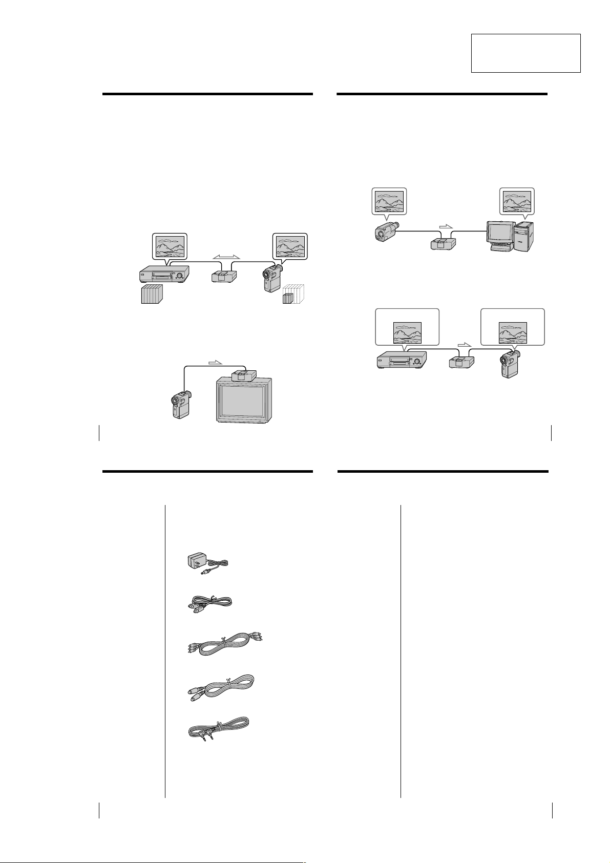
Using with an analog video unit
and a digital video unit
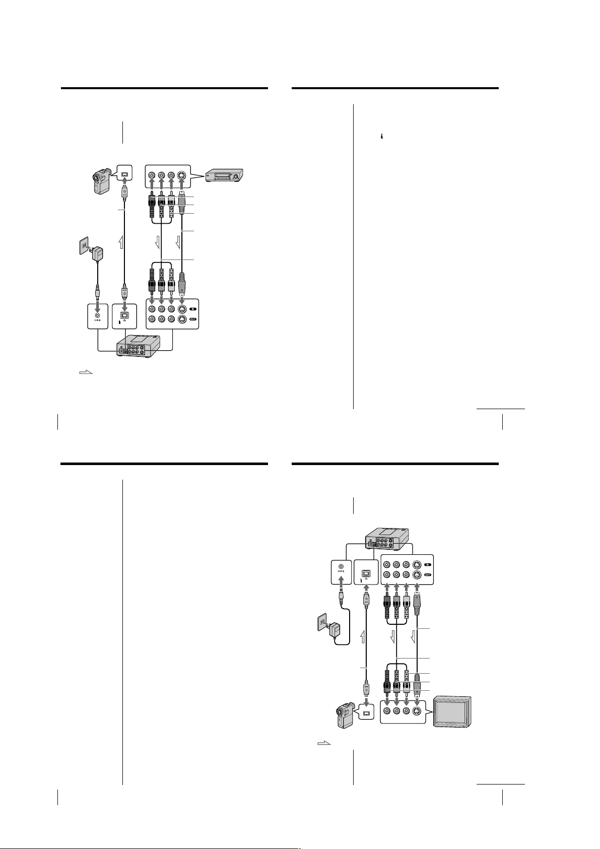
Connecting an analog video unit and
a DV unit via the media converter
Example: Converting analog video to digital video
to Audio/video output
to S VIDEO outputto DV input/output
DV
DV connecting cable
(supplied)
to AC outlet
AC power
adapter
(supplied)
DV IN/OUT
DC IN 6V
: Signal flow
-US
8
RL
AUDIO VIDEO S VIDEO
Audio R (red)
Audio L (white)
Video (yellow)
S VIDEO connecting cable
(supplied)
AV connecting cable (supplied)
Note
Depending on the
condition of the analog
video signal input to the
media converter, some
DV units may not output
the analog video signal
correctly when the digital
video signal is output
from the media converter.
The video recorded on the
DV unit is not affected.
When previewing a
recorded VIDEO ,we
recommend connecting
the input connector of the
TV to the VIDEO OUT or
S VIDEO OUT of the
media converter.
If you want to convert digital video to analog
video
Make the connection as follows:
• Connect the DV output connector of the DV unit to
the
DV IN/OUT connector of the media converter
using the supplied DV connecting cable.
• Connect the input connectors of the analog video
unit to the AUDIO/VIDEO OUT connectors of the
media converter using the supplied a AV connecting
cable.
Converting analog video to digital
video
You can convert and record pictures and sound from
an analog video unit to a DV unit by connecting both
units via the media converter.
1
Press POWER to turn on the media converter.
2
Press ANALOG IN.
The key indicator lights up.
3
Select the audio mode.
Each time you press and hold ANALOG IN for a
few seconds, the audio mode changes as follows.
16-bit mode (high quality sound): The key
indicator lights up in red.
12-bit mode (post sound recording): The key
indicator lights up in green.
4
Pause playback on the analog video unit slightly
ahead of the point from which you want to start
recording.
5
Pause recording on the DV unit at the point from
which you want to start recording.
For details on how to record, refer to the
instruction manual of your DV unit.
(If you use the SONY DCR-PC1/PC7/PC10, the
remote controller is necessary for recording
operations.)
6
Start playback on the analog video unit, then start
recording on the DV unit.
The picture and sound played back on the analog
video unit are recorded on the DV unit.
continued
-US
9
Using with an analog video unit and a digital video unit (continued)
Converting digital video to analog
video
You can convert and record pictures and sound from a
DV unit to an analog video unit by connecting both
units via the media converter.
For the connection, refer to “If you want to convert
digital video to analog video” on page 9.
1
Press POWER to turn on the media converter.
2
Press DV IN.
The key indicator lights up.
3
Pause playback on the DV unit slightly ahead of
the point from which you want to start recording.
4
Pause recording on the analog video unit at the
point from which you want to start recording.
5
Start playback on the DV unit, then start recording
on the analog video unit.
The picture and sound played back on the DV unit
are recorded on the analog video unit.
Viewing digital video
on your TV
Connecting a DV unit and a TV via the
media converter
to AC outlet
AC power adapter
(supplied)
DV connecting cable
(supplied)
to DV input/output
DC IN 6V
: Signal flow
DV IN/OUT
DV
to Audio/video input
to S VIDEO input
RL
AUDIO VIDEO S VIDEO
S VIDEO connecting cable
(supplied)
AV connecting cable
(supplied)
Video (yellow)
Audio L (white)
Audio R (red)
-US
10
continued
-US
11
1-2
Page 5
Viewing digital video on your TV (continued)
13
-US
RL
AUDIO VIDEO S VIDEO
DV
DV IN/OUT
DC IN 6V
LANC
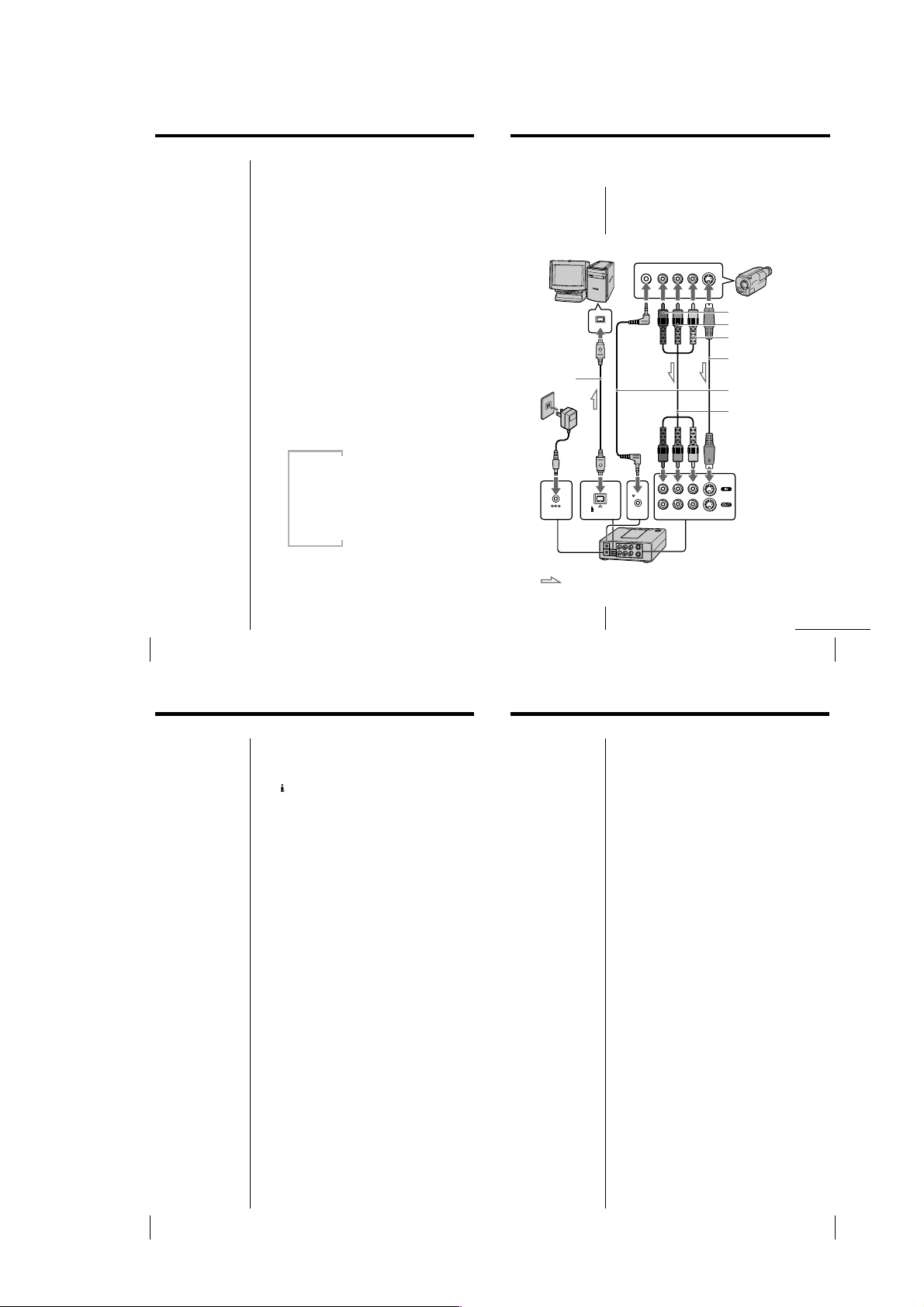
Connecting a PC and an analog video
unit via the media converter
Example: Capturing images from an analog video
unit using a PC.
to Audio/video output
to S VIDEO output
to LANC
Audio L (white)
Audio R (red)
Video (yellow)
S VIDEO connecting cable
(supplied)
AV connecting cable
(supplied)
DV connecting
cable (supplied)
: Signal flow
to AC
outlet
AC power
adapter
(supplied)
Using with an analog video unit
and a PC
to DV input/
output
continued
Note
On using the media converter and a PC for analog video
image editing, the PC must have DV image processing
software which is capable of video image capturing and rerecording with the analog video equipment through the
media converter.
LANC connecting cable
(supplied)
15
-US
Note
You cannot operate the
media converter from a
LANC compatible unit,
for example a remote
commander or remote
tripod.
Recording images from a PC to analog
video
1
Press POWER to turn on the media converter.
2
Press DV IN.
The key indicator lights up.
3
Start recording on the analog video unit.
You can operate the analog video unit from the PC
by the LANC connection. But some functions,
depending on the analog video unit, may not
work.
4
Start outputting procedures on your PC.
The operation procedures depend on your PC and
the software which you use.
For details on how to capture images and how to
operate the analog video unit from the PC, refer to
the instruction manual of your PC and software, or
ask your PC and software makers.
Viewing digital video on your TV
You can enjoy high quality digital video when you
connect the DV unit to the TV via the media converter.
1
Press POWER to turn on the media converter.
2
z Tip
TVs which conform to the
ID-1 system automatically
switch to wide mode
when the appropriate
signal is received.
Press DV IN.
The key indicator lights up.
3
Start playback on the DV unit.
Pictures played back on the DV unit appear on the
TV screen.
Playing back the audio while changing
the mixing rate
When playing back video recorded in 12-bit audio
mode on a DV unit via the media converter, you can
listen to: the recorded message and/or background
music only (post sound recording), the original audio,
or the combined audio of both tracks with the desired
mixing rate (5 steps).
Press and while holding DV IN, press ANALOG
IN.
Each time you press ANALOG IN, the mixing rate
changes as follows:
Original audio Added audio
m
100% 0%
m
75% 25%
Note
When the power on the
media converter is turned
off, the mixing rate is
reset to the default setting
(original audio: 100%,
added audio: 0%).
m
50% 50%
m
25% 75%
m
0% 100%
-US
12
Using with an analog video unit and a PC
z Tip
The DV still image
capture card kit DVBKCW200 for PC/AT
compatible or DV still
image capture board kit
DVBK-2000 (not
supplied) can be used.
For details, refer to the
operating instructions of
DV still image capture
card kit or DV still image
capture board kit.
1
For VAIO, DVgate
*
Motion Version 1.2 or
later
However, because the
LANC connection
cannot transfer the
track number data
(tape position of the DV
unit) to the PC, image
capturing by setting
IN/OUT of the DVgate
Motion is impossible.
For manual control,
select “Settings”–
“Select Device
Controller”–“Do not
control DV device with
DVgate Motion”.
2
For VAIO, DVgate
*
Motion Version 1.4.2 or
later
Select “Help”–“About
DVgate Motion...” of
DVgate Motion for
checking the software
version.
zTip
•For further information of
LANC, see page 24.
•DVgate Motion is the
software for the DV video
and audio import/export
bundled with VAIO.
-US
14
(continued)
If you want to convert captured images from
your PC to analog video
Make the connection as follows:
• Connect the DV output connector of the PC to the
DV IN/OUT connector of the media converter
using the supplied DV connecting cable.
• Connect the input connectors of the analog video
unit to the AUDIO/VIDEO OUT connectors of the
media converter using the supplied AV connecting
cable.
Capturing images from an analog
video unit using a PC
You can capture the images from an analog video unit
using a PC which is connected via the media
(*1)
converter.
Also, you can operate the analog video unit from the
PC by the LANC connection.
Compatible software is required for respective
operations in the PC.
1
Press POWER to turn on the media converter.
2
Press ANALOG IN.
The key indicator lights up.
3
Start playback on the analog video unit slightly
ahead of the point from which you want to start
capturing images.
You can operate the analog video unit from the PC
by the LANC connection. But some functions,
depending on the analog video unit, may not
work.
4
Start capturing procedures on your PC.
The operation procedures depend on your PC and
the software which you use.
For details on how to capture images and how to
operate the analog video unit from the PC, refer to
the instruction manual of your PC and software, or
ask your PC and software makers.
(*2)
1-3
Page 6
Precautions
-US
16
Use
• Operate the product only with the supplied AC power
adapter. If you use a different AC power adapter, it may
cause a malfunction.
Unified polarity plug
• Should any liquid or solid object fall into the cabinet,
unplug the product and have it checked by qualified
personnel before operating it further.
• Always turn the product off when not in use.
Unplug the product from the wall outlet if you are not
going to use it for several days or more. To disconnect the
cord, pull it out by the plug. Never pull the cord itself.
• Do not overload wall outlets, extension cords, or
convenience receptacles beyond their capacity, since this
can result in fire or electric shock.
• Do not use attachments not recommended by the
manufacturer, as they may cause hazards.
• Do not touch the AC power adapter with wet hands. If
you fail to observe this, it may cause electric shock.
• Do not drop or give a mechanical shock to the product.
Installation
• To prevent internal heat build-up, do not block the
ventilation openings.
• Avoid operating the product at temperatures below 5˚C
(41˚F).
• Do not subject the product to high temperature or direct
sunlight. If you do not observe the above instructions, the
product may become deformed.
• Do not place the product in locations where it is wet,
humid, dusty, smoky, or steamy. Do not use this product
near or around water. It may cause fire or electric shock.
Especially, do not use the product in the bathroom.
• If the product is transported directly from a cold to a warm
location, or if the room temperature has changed
suddenly, moisture may condense in the unit. If this
happens, let the moisture evaporate before using the
product.
• Do not place the product on an unstable cart, stand, table,
or shelf. The product may fall, causing serious injury to a
child or an adult, and serious damage to the product.
• Do not allow anything to rest on or roll over the power
cord, and do not place the product where the power cord
is subject to wear or abuse.
Others
• Unplug the product from the wall outlet and refer
servicing to qualified service personnel under the
following conditions:
- When the power cord or plug is damaged or frayed.
- If liquid has been spilled into the product.
- If the product has been exposed to rain or water.
- If the product has been subject to excessive shock by
being dropped, or the cabinet has been damaged.
- If the product does not operate normally when
following the operating instructions. Adjust only those
controls that are specified in the operating instructions.
Improper adjustment of other controls may result in
damage and will often require extensive work by a
qualified technician to restore the product to normal
operation.
- When the product exhibits a distinct change in
performance –– this indicates a need for service.
• Do not disassemble or modify the product. It may cause
fire or electric shock. Have the product checked and
repaired at your Sony dealer or local authorized Sony
service facility.
• Do not attempt to service the product yourself since
opening the cabinet may expose you to dangerous voltage
or other hazards. Refer all servicing to qualified service
personnel.
• When replacement parts are required, be sure the service
technician certifies in writing that he has used replacement
parts specified by the manufacturer that have the same
characteristics as the original parts.
Unauthorized substitutions may result in fire, electric
shock, or other hazards.
• Upon completion of any service or repairs to the product,
ask the service technician to perform routine safety checks
(as specified by the manufacturer) to determine that the
product is in safe operating condition, and to so certify.
• Unplug the product from the wall outlet before cleaning.
Clean the product with a dry, soft cloth, or a soft cloth
slightly moistened with a mild detergent solution. Do not
use any type of solvent, such as alcohol or benzine.
-US
17
Technical information
Signal flows
The signal flow of the media converter and the
connected unit is illustrated below:
When the media converter is turned off (with
the AC power adapter connected)
output
analog
signal
When the media converter is turned on
(When inputting analog signals)
output
analog
signal
convert to
digital
signal
When the media converter is turned on
(When inputting digital signal)
convert to
analog
signal
Analog signal
from the
ANALOG OUT
Analog signal to
the ANALOG IN
When you connect your TV to a VCR via
the media converter, you can watch VCR
pictures whenever the media converter is
not turned on.
Analog signal
from the
ANALOG OUT
Analog signal to
the ANALOG IN
Digital signal to
the
DV IN/OUT
The signals are output from both the
IN/OUT and ANALOG OUT connectors.
Analog signal
from the
ANALOG OUT
Digital signal to
DV IN/OUT
the
continued
DV
Technical information (continued)
Output/input of analog video signals
Depending on which connection is used, VIDEO IN or
S VIDEO IN, the output signal changes as follows.
The input signal is coming from only the VIDEO IN
connector
c The signal is output from the VIDEO OUT connector, but
not from the S VIDEO OUT connector.
The input signal is coming from only the S VIDEO IN
connector
c The signal is output both from the VIDEO OUT and S
VIDEO OUT connectors.
The input signal is coming from both the VIDEO IN and S
VIDEO IN connectors
c The signal is output both from the VIDEO OUT and S
VIDEO OUT connectors.
Notes
• When connecting to only the VIDEO IN connector, the
signal cannot be output to the S VIDEO OUT connector.
• When connecting both the S VIDEO IN and VIDEO IN
connectors, the S VIDEO signal is automatically selected
for converting the digital video signal regardless signal
type.
• For higher quality pictures, we recommend connecting
both the S VIDEO IN and S VIDEO OUT connectors.
Copyright precautions
On recording
When you play back video which includes copyright
protection signals and the playback signals are input
to the media converter, the PROTECT indicator on the
media converter lights up. In this case, You cannot
record or capture the video output from the media
converter.
ID-2 system
This copyright protection system is used for the analog
connection. The ID-2 system is added to the ID-1 system.
CGMS-D system
This copyright protection system is used for the digital
connection.
-US
21
-US
22
1-4
Page 7
DV recording format
24
-US
LANC (Local Application Control Bus System) is a
system to control other equipment. The data is
transported via the LANC connectors, and includes
the operation command, such as play, stop, and pause
as well as the status of the equipment.
is the label of the LANC.
• If your analog video unit has a LANC setting choice
of “M” (control side) or “S” (passive side), be sure to
select “S”.
• To control a video camera recorder with the LANC
connection, set the video camera recorder to “VTR”
mode.
• When you control an analog video unit from the PC,
some functions which the analog video does not
have may not be available.
Technical information (continued)
LANC connector
16-bit mode
The 16-bit mode uses the whole audio area to output
one stereo track. The original audio can be output
with high quality in this mode. This mode uses 48
kHz sampling frequencies.
12-bit mode
The 12-bit mode consists of two separate stereo tracks
– Stereo 1 and 2. This mode uses 32 kHz sampling
frequencies. With the DV unit, you can add messages
or background music independent from the recorded
sound in this mode.
12-bit/16-bit audio output modes
Macrovision
This product incorporates copyright protection technology
that is protected by method claims of certain U.S. patents and
other intellectual property rights owned by Macrovision
Corporation and other rights owners. Use of this copyright
protection technology must be authorized by Macrovision
Corporation, and is intended for home and other limited
viewing uses only unless otherwise authorized by
Macrovision Corporation. Reverse engineering from
disassembly is prohibited.
The following figure shows how the signals are
recorded on a DV tape.
10 tracks = 1 frame
ITI sector
Reference signals for
insert editing, etc.
Sub code sector
Index signals, time codes, etc.
Video sector
Video signals,
recording data,
etc.
Audio sector
Audio signals
16-bit audio mode
1 stereo track
12-bit audio mode
2 stereo tracks
Locating the parts and
controls
Front
12 3 4
Rear
9
8
7
56
continued
1 POWER button
Turns on/off the media converter.
2 PROTECT indicator
Lights when the input picture includes a
copy protection signal.
You cannot record the signal when this
indicator is lit.
3 ANALOG IN key and indicator
Select the signal input from the AUDIO/
VIDEO/S VIDEO IN as the input signal to
the media converter.
4 DV IN key and indicator
Select the signal input from the
OUT as the input signal to the media
converter.
5 DC IN 6V connector
Connect to the supplied AC power adapter.
6
DV IN/OUT connector
Connect to the DV unit.
7 AUDIO/VIDEO/S VIDEO OUT
connectors
Connect to the analog video unit or TV.
8 AUDIO/VIDEO/S VIDEO IN connectors
Connect to the analog video unit.
When you connect both the S VIDEO IN and
VIDEO IN connectors, the S video signal is
automatically selected.
When connecting to VIDEO IN connectors
only, no signals are output from the S
VIDEO OUT connector.
9
LANC connector
Connect to a video unit with a LANC
connector.
DV IN/
-US
23
-US
25
1-5E
Page 8
2-1. OVERALL BLOCK DIAGRAM
IFX-52 BOARD
(SEE PAGE 3-9 ~ 3-26)
J802
VIDEO IN
J802
S-VIDEO IN
LINE V
S C
S Y
34
25
33
IC102
AGC, AFC,
A-D CONV.
SECTION 2
BLOCK DIAGRAMS
51
Y0-Y7
58
61
C0-C7
68
HD
72
VD
73
AFCK
48
SPCKO
46
43
44
X101
40.5MHz
IC101
EVR
X401
13.5MHz
Y
C
17
IC401
12
9
8
BLOCKING
7
SHUFFLING
STILL FILTER
4
MEMORY FEATURE
109
DIGITAL EFFECT
106
TEST SIG.
ENCODER
105
104
101
50
61
68
DVMC-DA2
53
IC501
90
|
83
97
96
V BUS
TRCK
|
56
•
58
|
ESTIMATION
61
51
INTERLEAVE/
DEINTERLEAVE
DCT/IDCT
QUANTIZE
VLC/VLD
FRAMING
ADSP
90
|
L BUS
93
LCKO
11
TRCK
45
|
42
DV INTERFACE
79
47
IC503
6
|
9
27
•
29
|
32
•
34
|
37
TPA+, TPA–, TPB+, TPB–
IC601
FRRV
22
TRRV
23
X501
24.576MHz
13
14
44
45
39
71
|
74
T BUS
•
77
|
80
TRCK
IC502
5
|
12
ECC/PTG
DESHUFFLING
ENCODE/DECODE
CONCEAL
26
TBC
38
|
MC BUS
48
31
32
FRRV
TRRT
TRRV
26
MECHA
|
CONTROL
33
•
35
|
37
106
107
108
IC602
EEPROM
CN801
DV IN/OUT
J802
VIDEO OUT
J802
S-VIDEO OUT
LINE V
S C
S Y
LINE V
S Y
S C
1
3
7
12
15
IC002
VIDEO
SWITCH
IC001
LINE OUT
AMP
1 2
SCK
SO
74SO75
UNREG
EVER 5V
EVER 5V AU
EVER 3V AOI
EVER 3V AU
2V
SW 5V
VFD 3V
A 3V
SW 3V
7681 83 82
(SEE PAGE 3-2)
50
49
84 85 86
33 34 35
IC703
HI CONTROL
SCK
SCK
SO
SI
SO
SI
38
40
41
60
27
28
29
30
2
VDD
XRESET
X701
20MHz
POW ON
DD 34 ON
DD 2 ON
DD PWR ON
LANC JACK IN
LANC IN
LANC OUT
6
5
101
12
IC701
VDO SWITCH
RESET
IC702
LANC I/F
4
SCK
SO
SI
7
14
11
UNREG
2
2
3
3
4
4
JK-02 BOARD
115 116 11776 75 74 14 13
SCK
SO
SI
7
27
31
Y
25
C
29
DATA
SCK
12
9
IC704
SWITCH
SCK
SO
SI
13
SCK STB
14
10
DATA STB
11
SCK
2 3 4
SI
IC301
DC-DC
CONV.
J301
DC IN 6V
J801
LANC JACK
J802
AUDIO L IN
AUDIO R IN
AUDIO L OUT
AUDIO R OUT
16 15
L
R
L
R
34
36
37
38
IC201
AUDIO I/O
28
26
24
20
L
R
L
R
6
3
19
20
IC202
A-D CONV.
D-A CONV.
12
DATA FROM SFD
15
11
DATA TO SFD
SFD BCK
XLANC ON
12
80
ERR LED, ANALOG LED, DV LED, MS LED
|
83
94
95
•
KEY AD1, KEY AD2
SWX-22 BOARD
(SEE PAGE 3-2)
3
3
|
|
6
6
9
9
•
•
10
10
S901, S902, S905
ANALOG IN SW
DV IN SW
POWER SW
D901-D903
ANALOG IN LED
DV IN LED
PROTECT LED
2-1 2-2
Page 9
DVMC-DA2
2-2. POWER BLOCK DIAGRAM
IFX-52 BOARD
(SEE PAGE 3-9 ~ 3-26)
J301
DC IN 6V
J801
LANC JACK
D701
JK-02
BOARD
(SEE PAGE 3-2)
PS701
LF301
IC301
FL301FB301 FB302 F301
IC701
3
7
REG
BATTERY IN
DETECT
RESET
5
6
4
8
DC-DC CONV.
VCC1
VCC2
CTL1
CTL2
20 21 22
L701
OUT1
+IN1(E)
OUT2
+IN2(E)
OUT3
-IN3(E)
CTL3
FL701
18 46
45
IC702
LANC I/F
1
UNREG
14
LANC DC
33
11
LANC SIG
44
22
VCC
POWER
8
Q701
4
Q302
SWITCHING
7
Q304
SWITCHING
44
12
Q303
SWITCHING
40
26
L305 L313
D302
L307
D304
L306
D303
Q308
Q305
L312
L314
L315
L311
L316
L309
L310
L308
EVER 5V
EVER 5V AU
SW 5V
EVER 3V AOI
EVER 3V AU
VFD 3V
A 3V
SW 3V
2V
VFD 3V
SW 3V
SW 3V
2V
SW 3V
L505
L503
L502
L501
FL501
FL505
FL504
FL503
IC703
HI CONTROL
POW ON
KEY AD1
60
EVER 3V AOI
EVER 5V
L001,L002
IC001
IC002
94
27
28
29
38
31•42•51
62•63•65
86•87•92
61
12
30
DD 34 ON
DD 2 ON
DD PWR ON
XRESET
VDD
BATT IN
XLANC ON
XLANC JACK IN
IC704
SWITCH
VCC
16
LINE OUT
AMP
VIDEO
SWITCH
L401, L403
IC503
DV INTERFACE
IC501
DCT/IDCT
ESTIMATION
QUANTIZE
VLC/VLD
FRAMING
DEFRAMING
MEMORY FEATURE
FL402
IC502
ECC/PTG
DESHUFFLING
ENCODE/DECODE
CONCEAL
TBC
IC401
BLOCKING
SHUFFLING
STILL FILTER
DIGITAL EFFECT
TEST SIG.
ENCODER
FL401
L402
FL404
X401
13.5MHz
SW 3V
SW 5V
A 3V
EVER 5V AU
EVER 3V AU
L201, L202, L203
SW 3V
EVER 5V
L106
L101
L102
L601
FB747
FB748
FL101
Q205, Q207
FL601
8
IC101
EVR
IC102
AGC, AFC,
A-D CONV.
IC201
AUDIO I/O
IC202
AUDIO
ADC&DAC
IC601
MECHA
CONTROL
IC602
EEPROM
SWX-22 BOARD
(SEE PAGE 3-2)
11
8
99
EVER 5V
3V
LED
FUNCTION
SWITCH
S901
POWER
2-3 2-4E
Page 10
SECTION 3
PRINTED WIRING BOARDS AND SCHEMATIC DIAGRAMS
DVMC-DA2
THIS NOTE IS COMMON FOR WIRING BOARDS
AND SCHEMATIC DIAGRAMS
(In addition to this, the necessary note is printed
in each block)
(For printed wiring boards)
• b: Pattern from the side which enables seeing.
(The other layers' patterns are not indicated.)
• Through hole is omitted.
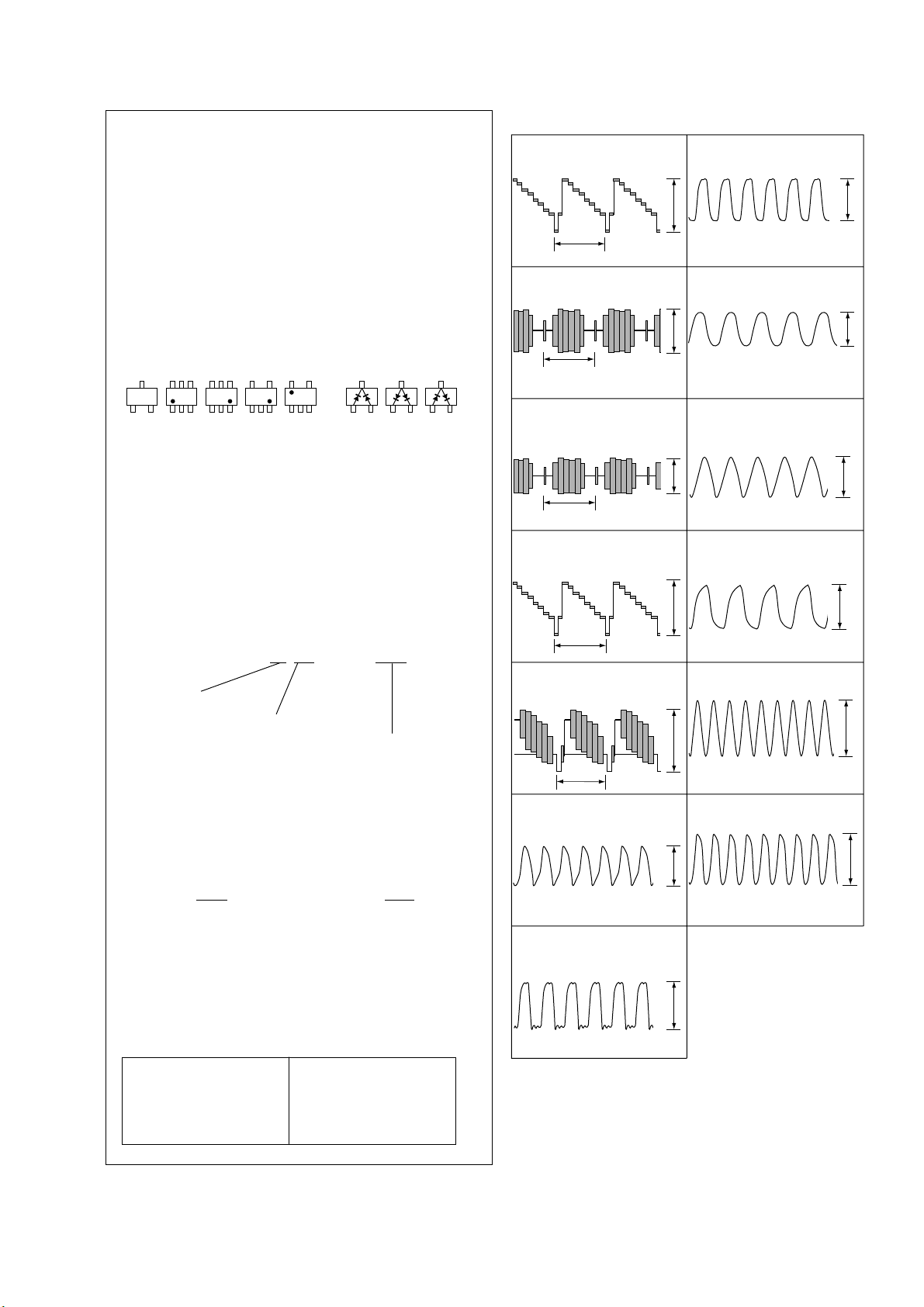
• Circled numbers refer to waveforms.
• There are few cases that the part printed on diagram
isn’t mounted in this model.
• Chip parts.
C
BE
(For schematic diagrams)
• All capacitors are in µF unless otherwise noted. pF : µ
µF. 50V or less are not indicated except f or electrolytics
and tantalums.
• Chip resistors are 1/10W unless otherwise noted.
kΩ=1000Ω, MΩ=1000kΩ.
• Caution when replacing chip parts.
New parts must be attached after removal of chip.
Be careful not to heat the minus side of tantalum
capacitor, Because it is damaged by the heat.
• Some chip part will be indicated as follows.
Example C541 L452
5
64
2
13
Transistor
5
45
46
2
31
31
12
2
4
53
3
21321321
22U 10UH
TA CH 2520
Diode
• Wavef orm
1
IC001 qh YOUT
H
2
IC001 qs COUT
H
3
IC102 wg AGCCIN
(S-VIDEO : IN)
H
4
IC102 ed ANIN1
(S-VIDEO : IN)
H
1.7Vp-p
1.4Vp-p
240mVp-p
370mVp-p
8
IC401 t; SPCK(CL403)
13.5MHz
9
IC501 qf XOO(R510)
24.576MHz
0
IC501 e; POO
(L504 – C509)
31.33MHz
qa
IC501 qa LCKO(CL505)
IC503 ul X1(CL505)
24.576MHz
3Vp-p
2.3Vp-p
2.5Vp-p
2.8Vp-p
Kinds of capacitor
Temperature characteristics
External dimensions (mm)
• Constants of resistors, capacitors, ICs and etc with XX
indicate that they are not used.
In such cases, the unused circuits may be indicated.
• Parts with ★ differ according to the model/destination.
Refer to the mount table for each function.
• All variable and adjustable resistors have characteristic
curve B, unless otherwise noted.
• Signal name
XEDIT→ EDIT PB/XREC → PB/REC
• 2: non flammable resistor
• 1: fusible resistor
• C: panel designation
• U : B+ Line
• V : B– Line
• N : IN/OUT direction of (+,–) B LINE.
• C: adjustment for repair .
• Circled numbers refer to wav eforms.
Note :
The components identified by
mark 0 or dotted line with mark
0 are critical for safety.
Replace only with part number
specified.
Note :
Les composants identifiés par
une marque 0 sont critiques
pour la sécurité.
Ne les remplacer que par une
pièce portant le numéro spécifié.
5
IC102 ef ANIN2
(Composite VIDEO : IN)
H
6
IC102 rd VCXD0
7
IC401 <z/z
IC102 rk CLKP(CL101)
13.5MHz
410mVp-p
5.2Vp-p
VCXD0(CL401)
3Vp-p
qs
IC601 1 XO
20MHz
qd
IC703 r; 20MHz OUT
20MHz40.5MHz
1.8Vp-p
3Vp-p
3-1
Page 11
DVMC-DA2
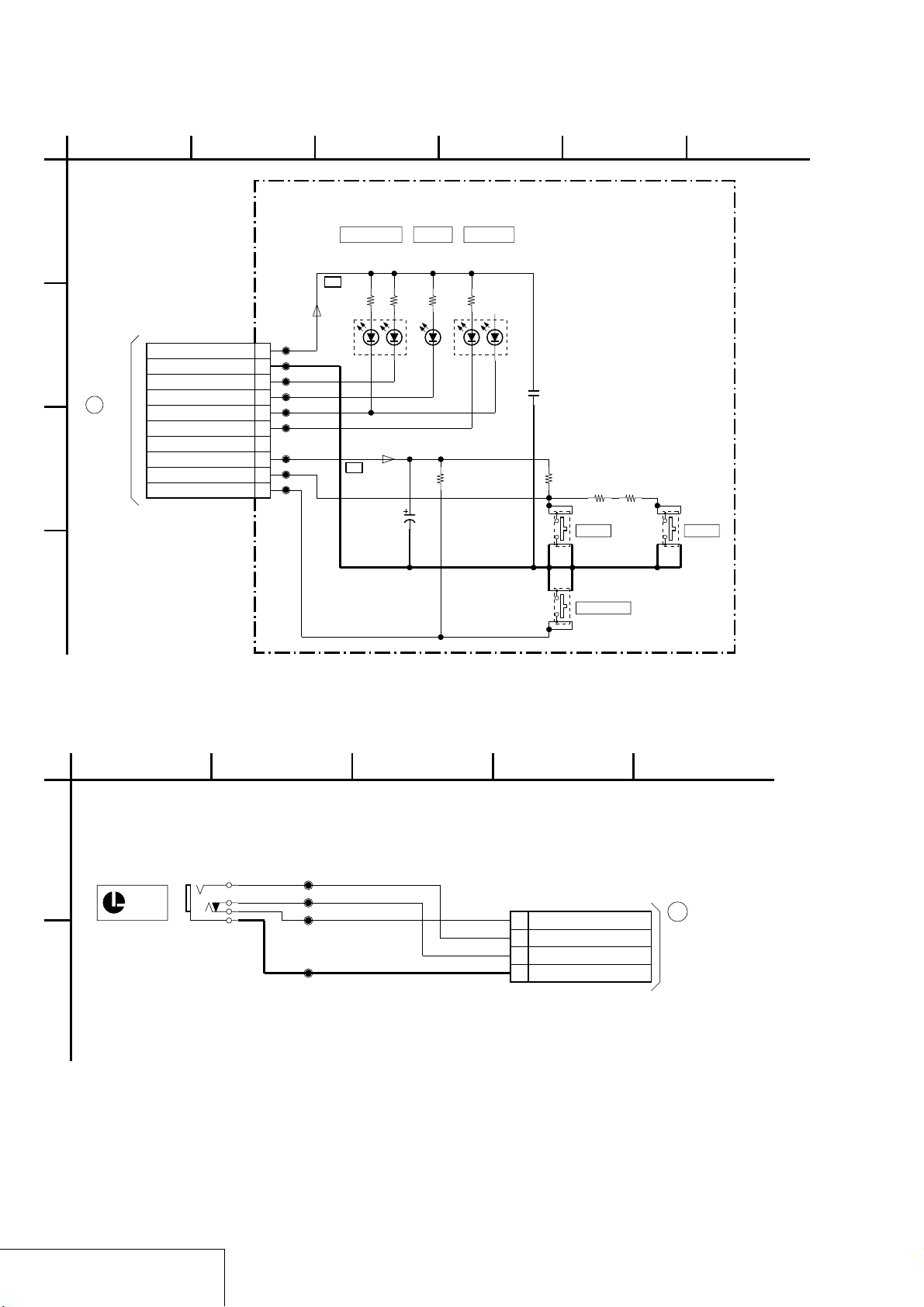
SWX-22 (SWITCH) SCHEMATIC DIAGRAM
1
23 6
4
5
SWX-22 BOARD
A
10PCN901
JL901
B
A
TO
IFX-52
BOARD
CN701
C
D
16
1EVER_5V_SW
JL902
2GND_SW
JL903
3ANALOG_LED
JL904
4DV_LED
JL905
5MS_LED
JL906
6ERR_LED
7XSIRCS_IN
JL908
8RSTEVER_3V
JL909
9KEY_AD1
JL910
10KEY_AD2
ANALOG IN DV IN PROTECT
R912
B+
D903
R914
150
2012
CL-155SD/G-D-T
ORGK
B+
2012
C901
22u
R901
150
180
2012
GRNK
4V
D901
R903
R902
150
2012
CL-170G-CD-T
RED
10k
2012
GRN
D902
CL-155UR/G-DT
C902
0.01u
2012
B
R905
10k
2012
R908
R906
1500
1200
2012
2012
S901
POWER DV_IN
S902
ANALOG_IN
S905
JK-02 (LANC JACK) SCHEMATIC DIAGRAM
1
JK-02 BOARD
A
J881
LANC
JL885
JL886
JL887
JL888
B
16
4
3
2
1
4
LANC_SIG
LANC_DC
LANC_JACK IN
GND
CN893
4P
B
TO
IFX-52
BOARD(9/10)
CN802
(SEE PAGE
325
3-25)
SWITCH
SWX-22
LANC JACK
/
JK-02
3-2
Page 12
DVMC-DA2
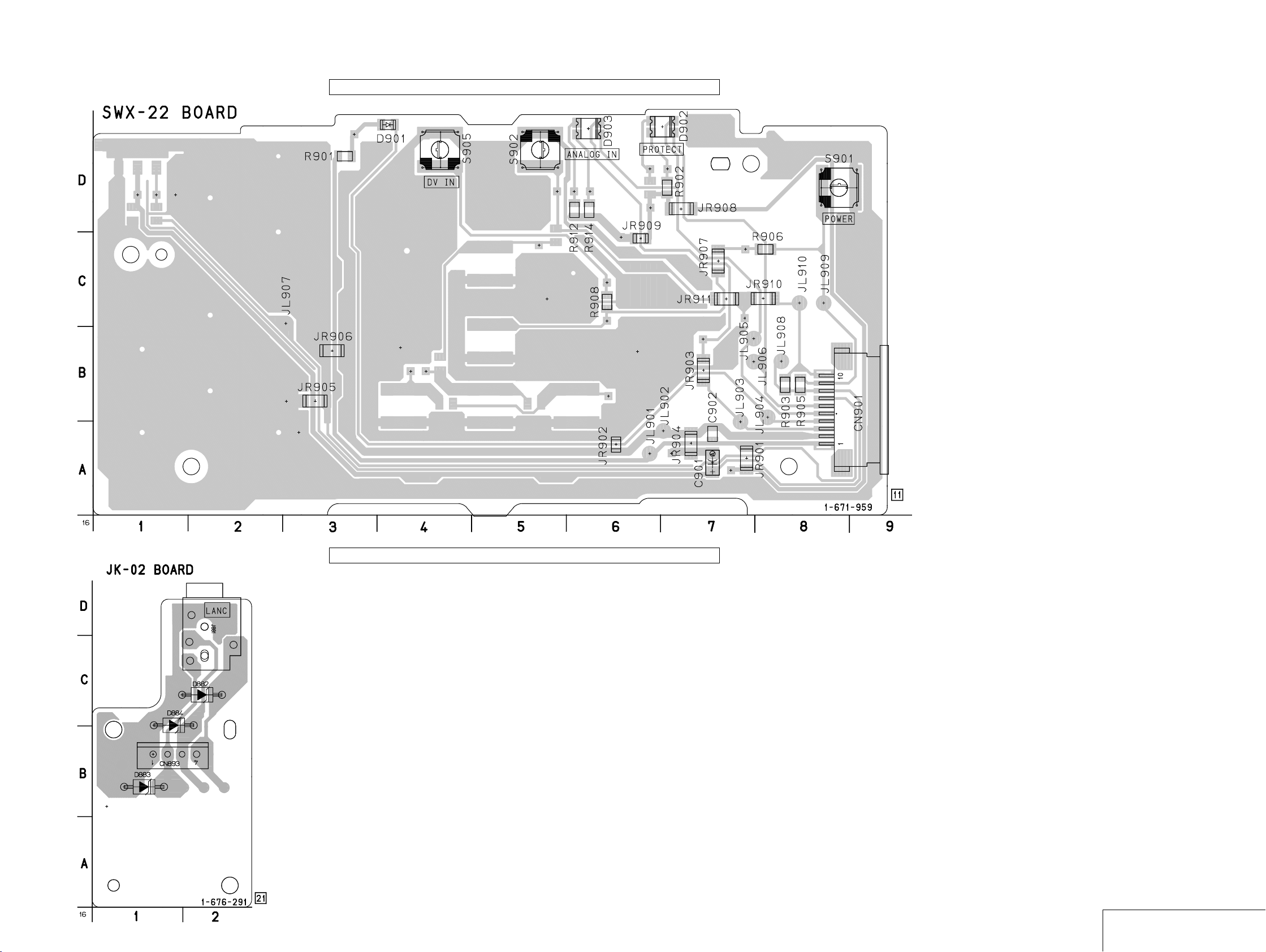
SWX-22 (SWITCH) PRINTED WIRING BOARD
There are few cases that the part printed on this diagram isn’t mounted in this model.
JK-02 (LANC JACK) PRINTED WIRING BOARD
There are few cases that the part printed on this diagram isn’t mounted in this model.
3-3 3-4
SWITCH
SWX-22
LANC JACK
/
JK-02
Page 13

DVMC-DA2
IFX-52 (MAIN : SIDE A) PRINTED WIRING BOARD
IFX-52 BOARD
D302 C-1
D303 C-2
D304 C-1
D702 B-6
D703 C-8
D705 C-8
D706 C-9
D707 D-8
D801 A-2
D802 A-2
IC001 E-6
IC101 C-7
IC201 D-4
IC202 C-6
IC301 B-1
IC502 A-4
IC701 A-6
IC702 B-6
IC703 B-7
Q101 D-7
Q102 D-7
Q103 E-7
Q104 E-7
Q105 E-7
Q106 D-7
Q107 D-7
Q108 D-7
Q109 D-7
Q201 F-4
Q202 F-4
Q203 F-4
Q205 E-4
Q206 E-3
Q207 E-3
Q208 E-3
Q209 C-5
Q302 C-1
Q303 C-2
Q304 C-1
Q305 D-2
Q306 D-2
Q307 B-3
Q308 B-2
Q701 A-6
Q951 A-2
There are few cases that the part printed on this diagram isn’t mounted in this model.
MAIN
IFX-52
3-5 3-6
Page 14

DVMC-DA2
IFX-52 (MAIN : SIDE B) PRINTED WIRING BOARD
There are few cases that the part printed on this diagram isn’t mounted in this model.
IFX-52 BOARD
D101 E-1
D102 E-1
D501 D-6
D701 A-3
IC002 E-4
IC102 D-2
IC401 C-3
IC501 C-5
IC503 E-7
IC601 B-4
IC602 B-5
IC704 A-1
Q003 E-5
Q004 E-4
Q110 D-3
Q702 B-1
Q703 B-1
Q704 B-1
Q705 B-1
3-7 3-8
MAIN
IFX-52
Page 15

DVMC-DA2
IFX-52 (J CORE) SCHEMATIC DIAGRAM • Refer to page 3-5, 3-7 for IFX-52 BOARD printed wiring board. • Refer to page 3-1 for waveforms.
1
IFX-52 BOARD(1/10)(J CORE)
A
D:DV IN,VIDEO OUT mode
A:VIDEO IN,DV OUT mode
No mark:Same regardless of modes
13
TO(10/10)
(SEE PAGE
3-26E)
B
12
TO(2/10)
(SEE PAGE
3-11)
C
D
1
TO(8/10)
(SEE PAGE
3-23)
E
2
(SEE PAGE
3-11)
3
(SEE PAGE
3-18)
TO(2/10)
TO(5/10)
F
G
4
(SEE PAGE
3-12)
TO(2/10)
H
I
J
5
(SEE PAGE
3-13)
TO(3/10)
K
L
M
SFD_LRCK
DATA_TO_SFD
DATA_FROM_SFD
DATA_FROM_MS_VSP
DATA_TO_MS_VSP
XMS_SCK_VSP
XRST_VSP
LIP_SLEEP
XRST_LINK
XRST_PHY
2
SFD_FCK
SFD_BCK
XCS_SFD
DXXA10
D24A00
D25A01
D26A02
D27A03
D28A04
D29A05
D30A06
D31A07
DXXA08
DXXA09
SW_3V
VBUS0
VBUS1
VBUS2
VBUS3
VBUS4
VBUS5
VBUS6
VBUS7
XDVCN
TDO4
TDO2
TUVS
XVEN
TUSV
TRCK
WR01
FRRV
TRRT
TCK
TMS
L2V
L3V
2V
GND
RDX
DRP
SWP
ALE
LPS
OFR
DATA_FROM_MECHA
DATA_TO_MECHA
XMECHA_SCK
XRST_VSP
LIP_SLEEP
XRST_LINK
XRST_PHY
LRCK0
ADAO1
VBUS0
VBUS1
VBUS2
VBUS3
VBUS4
VBUS5
VBUS6
VBUS7
XCS_SFD
DXXA10
D24A00
D25A01
D26A02
D27A03
D28A04
D29A05
D30A06
D31A07
DXXA08
DXXA09
XDVCN
5 1712 15 2019
74
9
138 22
14
16
183 11106
21
B+
B+
C511
12p
GND
VBUS054VBUS155VBUS256VBUS3
53
VBUS0
VBUS1
VBUS2
VBUS3
9
CH
TMS
VDDL
57
58
VBUS4
VBUS459VBUS560VBUS661VBUS7
TDO4
TCK
TMS
TDO2
R501
47
C501
2.2u
6.3V
TA
A
C502
0.047u
B
1608
3
C503
0.001u
KV1470TL1-3
B
L501
FL503
10uH
FCK0
BCK0
ADAI1
C508
R503
CL501
0.001u
B
330
R502
4700
R504
L504
10k
1.5uH
1
R505
2
D501
10k
C509
0.001u
B
C507
C505
10u
0.01u
6.3V
B
TA
A
FCK0
LRCK0
BCK0
B+
B+
L502
10uH
B+
L503
10uH
B+
TUVS
XVEN
TUSV
18M
FL504
FL505
ADAI1
ADAO1
C506
C504
10u
10u
6.3V
6.3V
TA
TA
B+
10
GND
26
PCO
27
VDDH
28
POI
29
POO
30
GND
31
OCKO
32
VDDL
33
OCK
34
GND
35
0R506
FCKO
36
LRCKO
37
0
R507
VDDH
38
R508
0
BCKO
39
GND
40
BCK
R510
220
41
VDDL
42
LRCK
43
ADAI1
44
ADAO1
45
ADAI2
46
ADAO2
47
DRP
48
INIT
49
GND
50
TRCK
51
52
R509
0
B+
B+
WR01
RDX
FRRV
TRRT
DRP
SWP
ALE
LPS
FP
TCK
VBUS5
24.576MHz
R510
560
VBUS6
X501
14
15
GND16ECKI17TCK18TMS19TRST20VDDL21APRFF22MO023MO124TS025TS1
XOO
IC501
DCT/IDCT
ESTIMATION
QUANTIZE
VLC/VLD
FRAMING
ADSP
INTERLEAVE/
DEINTERLEAVE
HG73C050BPTL
62
VBUS7
IC501
GND
63
TUVS
C512
12p
CH
0R512
TUVS64XVEN65TUSV
XVEN
TUSV
ALE
DIR
FRL
FCLR
XENA
XACC
B+
XRST_VSP
3
4
1
R513
GND2XRST
VDDH5FRL6FCLR7DIR8XENA9XACC10VDDL11LCKO12GND13XOI
RAMTEST
LBUS3
LBUS2
LBUS1
LBUS0
XCS_SFD
XMECHA_SCK
TBUS7
TBUS6
TBUS5
TBUS4
TDO2
TDO3
FL501
L505
10uH
XRST_VSP
B+
B+
B+
TDI
100
TDO
99
PTEST
98
NC3
97
NC2
96
NC1
95
VDDL
94
LBUS3
93
LBUS2
92
LBUS1
91
LBUS0
90
GND
89
VDDH
88
XMCS
87
MSCK
86
DATA_FROM_MECHA
MSO
85
DATA_TO_MECHA
MSI
84
VDDL
83
NC
82
VDDL
81
TBUS7
80
TBUS6
79
TBUS5
78
TBUS4
77
GND
76
SEN
TUTL
TUTS
VDDL
66
67
68
69
70
SEN
TUTS
VDDL
TBUS072TBUS173TBUS274TBUS3
71
TBUS0
TBUS1
GND
75
C513
0.01u
B
TBUS2
TBUS3
0
XENA
FRL
FCLR
C515
C514
0.01u
6.3V
B
TA
B+
TUTS
TBUS0
TBUS1
TBUS2
TBUS3
TBUS4
TBUS5
TBUS6
TBUS7
SEN
1.8
41
D0.5/A2.2
LBUS3
LBUS2
LBUS1
LBUS0
10u
FP
A
1.8
0
0.3
0.3
0.3
0.3
0.3
0.3
0.3
0.3
0.3
0.01u
42
D0.5/A2.2
43
D0.5/A2.2
44
D0.5/A2.2
45
46
1.4
47
48
1.7
49
0
50
0
51
0
52
2.9
53
54
55
56
57
58
59
60
C517
0.01u
1
VDD
2
VSS
3
NC
4
TUTS
5
TBUS0
6
TBUS1
7
TBUS2
8
TBUS3
9
TBUS4
10
TBUS5
11
TBUS6
12
TBUS7
13
SFDEN
14
CRCK
15
TXDT0
16
TXDT1
17
TXDT2
18
TXDT3
19
TXDT4
20
TXST
21
HPCK
22
XTSY
23
XTDT0
24
XTDT1
25
NC
R514
0
C516
B
DIR
XACC
D31A07
D30A06
D29A05
D28A04
D27A03
D2.9/
A2.4
0.9
1.3
0.4
1.2
0.2
2.8
32
33
37
38
39
40
DA434DA535DA636DA7
VSS
XDIR
XIACC
VDD2
D2.9/A0
ID3
ID2
ID1
ID0
VSS
ICLK
VSS
XINEN
FR
OFR
IFCLEAR
VDD3
TEST0
TEST1
TEST2
TEST3
TEST4
TEST5
TEST6
TEST7
VDD362VSS63TMP064TMP165TMP266TMP367LPS68TM069TM170VDD271VSS72ENEC73AVD374PLLFLT75AVS76VDD377VSS78XI79XO
61
2.9
R516
0
B
TCK
TMS
TDO4
TDO3
0
1.802.8
2.8
100
TCK
VDD3
IC503
DV INTERFACE
SN104266PN-TEB
2.9
0
R517
CL505
11
LPS
1.8
IC502
ECC/PTG
DESHUFFLING
ENCODE/DECODE
CONCEAL
TBC
IC502
CXD3129R-T6
VSS
VDD
WRX
TRCK
26
27
28
29
30
1.4
1.8
2.8
2.8
WR01
ALE
RDX
31
0.5
RDX
VSS
DRP
VDD
SWP
FRRV
TRRT
32
33
1.4
1.4
TRRT
FRRV
MCCE
34
35
36
37
38
0
1.4
2.5
1.8
CL502
DRP
ALE
DXXA10
SWP
RDX
R526
WR01
28
0.4
0
D27A03
DXXA10
2.5
2.9
0.6
D28A04
0
2.8
2.8
0
23
24
25
26
ALE
XCS27VSS
XRD
XINT
XRW
1.2
2.9
0
R524
CL503
1.2
1.0
1.3
2.2
D29A05
D30A06
D31A07
DXXA08
D25A01
D24A00
D26A02
1.5
1.2
2.5
DA029DA130DA231DA3
IC503
2.9
1.8
R521
MCDA040MCDA141MCDA242MCDA343MCDA444MCDA545MCDA646MCDA747MCHA048MCHA1
39
1.2
2.4
1.5
D24A00
D25A01
D26A02
22
1.8
1.2
2.1
DXXA09
2.8
21
VDD2
80
R525
C519
2.8
49
XRST_LINK
XRESETL
0
0.1u
B
76
AVS0
50
2.8
B+
VSS
20
XRESETP
TPBIAS
0
CNA
19
2.8
18
0
PWD
17
2.9
VDD3
16
1.8
VDD2
15
AVS
14
2.9
AVD3
13
2.9
AVD3
12
1.2
R1
11
0
R0
10
1.8
9
TPA+
1.8
8
TPA-
1.8
7
TPB+
1.8
6
TPB-
2.9
5
AVD3
1.8
4
0
3
AVS
2.9
2
AVD3
1
AVS
XDVCN
XRST_PHY
LIP_SLEEP
TPA+
TPA+
6
TPA-
TPB+
±
0.5%12kR532
R535
12k
±
0.5%
R539
R538
56
56
±
±
0.5%
R536
0
CL504
R533
0
0.5%
C522
1u
B
2012
R541
56
±
R542
R540
10k
10k
±
±
0.5%
TPB-
TPA+
TPA-
TPB+
TPB-
R543
56
0.5%
±
0.5%
C523
220p
0.5%
CH
TO(9/10)
TPA-
TPB+
(SEE PAGE
3-25)
TPB-
B+
B+
B+
C521
0.01u
B
SIGNAL PATH
AVS177AVD178TTIM279TTIM180TTIM081TDAT782TDAT683TDAT584TDAT485TDAT386TDAT287TDAT188TDAT089VDD90VSS91MDFIX92FIXRP93XBIM94XSCAN95TMS96TDI97TDO98VDD99VSS
2.8
AVDD5
75
AVSD5
74
NC
73
NC
72
XDRT
71
2.8
SCL
70
2.8
AVDD4
69
AVSD4
68
TSEL0
67
TSEL1
66
2.8
AVDD3
65
AVSD3
64
TSEL2
63
TSEL3
62
XTSEL
61
2.8
TRST
60
2.8
XRST
59
TSEL4
58
TSEL5
57
2.8
AVDD1
56
AVSD1
55
TSEL6
54
TSEL7
53
2.8
AVDD0
52
AVSD0
51
AVD0
REC
PB
B+
VIDEO SIGNAL
CHROMA SIGNAL
Y/CHROMA
Y
AUDIO
N
16
J CORE
IFX-52
3-9 3-10
Page 16

IFX-52 (VFD) SCHEMATIC DIAGRAM • Refer to page 3-5, 3-7 for IFX-52 BOARD printed wiring board. • Refer to page 3-1 for waveforms.
DVMC-DA2
1
IFX-52 BOARD(2/10)(VFD)
A
7
TO(5/10)
(SEE PAGE
3-18)
B
2
TO(1/10)
(SEE PAGE
3-9)
8
TO(7/10)
C
(SEE PAGE
3-22)
D
E
9
F
TO(7/10)
(SEE PAGE
3-22)
G
H
23 11106
VFD_3V
L2V
L3V
GND
AFCK
SPCK0
B+
L401
100uH
2520
FL401
B+
B+
13.5M
ANALOG GND
DIGITAL GND
FL402
C401
0.01u
B
B+
7
CAM_FLD
CAM_VD
CAM_HD
CAM_C7
CAM_C6
CAM_C5
CAM_C4
TDO
TDI
TCK
TMS
DATA_TO_MS_VSP
DATA_FROM_MS_VSP
XMS_SCK_VSP
XCS_VFD
VFI_Y0
VFI_Y1
VFI_Y2
VFI_Y3
VFI_Y4
VFI_Y5
VFI_Y6
VFI_Y7
VFI_C0
VFI_C1
VFI_C2
VFI_C3
VFIO_C4
VFIO_C5
VFIO_C6
VFIO_C7
VFI_HD
VFI_VD
VFI_OE
CAM_Y0
CAM_Y1
CAM_Y2
CAM_Y3
CAM_Y4
CAM_Y5
CAM_Y6
CAM_Y7
CAM_C0
CAM_C1
CAM_C2
CAM_C3
CAM_C4
CAM_C5
CAM_C6
CAM_C7
CAM_HD
CAM_VD
CAM_FLD
5 12
C403
C404
220u
0.01u
4V
B
TA
C
C402
0.01u
B
91
LVDD3
92
VSS5
93
HVDD3
94
PLLTES
95
TEST
CL401
96
TRCKI
97
TRCKO
98
VSS6
99
VREF
100
OEI
101
AFCK
102
LVDD4
103
VSS7
104
VI
105
HI
106
CIOB3
107
CIOB2
108
CIOB1
109
CIOB0
110
SCAN
111
TDO
112
TDI
113
TCK
114
TMS
115
MSI
116
MSO
117
MSCK
118
XMCS
119
VSS8
120
HVDD4
R401
0
VBUS0
90
VBUS0
VBUS1
89
VBUS1
VBUS2
88
VBUS2
VBUS3
87
VBUS3
VBUS4
86
VBUS4
VBUS5
85
VBUS5
VBUS6
84
VBUS6
VBUS7
83
VBUS7
74
TUSV
TUVS
XVEN
70
71
72
73
74
75
76
77
78
79
80
VSS4
TUSV81TUVS82XVEN
LVDD2
AVDD5
CBDP
AVSS5
CRDP
AVDD4
YDP
AVSS4
IREFDP
R402
9
3300
100k
66
67
68
69
COUT
IREFC
AVSS3
AVDD3
R403
R404
3300
62
63
64
65
IREFY
AVSS2
AVDD1
AVDD2
IC401
BLOCKING
SHUFFING
STILL FILTER
MEMORY FEATURE
DIGITAL EFECT
TEST SIG
ENCODER
IC401
M65511AWG-600D
M65511FP
RVSS12RVDD13XRST4CIOA35CIOA26CIOA17CIOA08YI79YI610RVSS211RVDD212YI513YI414YI315YI216YI117YI018RVDD319RVSS320RVDD421RVSS422FRRV23TRRV24XSWE25SSS26COL027COL128COL229RVDD530RVSS5
1
138
B+
R410
R411
680
330
61
YOUT
60
AVSS1
59
PVSS
58
PVDD
57
HVDD2
56
VSS3
55
TSCK0
54
F358
53
DPVD
DPHD
OEO
SPCK
LVDD1
VSS2
VO
HO
YO7
YO6
YO5
YO4
YO3
YO2
YO1
YO0
OSDVD
OSDHD
OSDL
OSDP
COL3
HVDD1
VSS1
8
52
51
CL403
50
49
48
47
46
45
44
43
42
41
40
39
38
37
36
35
34
33
32
31
R406
0
L403
100uH
2520
C406
1u
2012
B+
R407
10k
R408
10k
R409
10k
C407
0.01u
VBUS0
VBUS1
VBUS2
VBUS3
VBUS4
B
VBUS5
VBUS6
VBUS7
TUVS
XVEN
TUSV
18M
B
C_OUT
Y_OUT
VBUS0
VBUS1
VBUS2
VBUS3
VBUS4
VBUS5
VBUS6
VBUS7
TUVS
XVEN
TUSV
TRCK
LINE_OUT_V
14
TO(6/10)
(SEE PAGE
3-19)
4
TO(1/10)
(SEE PAGE
3-9)
15
TO(4/10)
(SEE PAGE
3-15)
I
J
10
TO(3/10)
(SEE PAGE
3-13)
11
TO(10/10)
(SEE PAGE
3-26E)
12
TO(1/10)
(SEE PAGE
3-9)
16
XMS_SCK_VSP
XCS_VFD
DATA_TO_MS_VSP
DATA_FROM_MS_VSP
XRST_VSP
VREF
FRRV
TRRV
TMS
TDO1
TDO2
B+
B+
VFD
IFX-52
R416
0
R405
13.5MHZ
0
X401
L402
82nH
FL404
C405
0.01u
1608
B
XRST_VSP
R417
XMS_SCK_VSP
XCS_VFD
DATA_TO_MS_VSP
DATA_FROM_MS_VSP
XRST_VSP
TMS
TCK
TCK
TDI
TDO
CAM_C3
CAM_C2
CAM_C1
CAM_C0
CAM_Y7
CAM_Y6
CAM_Y5
CAM_Y4
CAM_Y3
CAM_Y2
CL402
CAM_Y1
CAM_Y0
SIGNAL PATH
VIDEO SIGNAL
CHROMA
REC
10k
10k
10k
R418
R419
Y/CHROMAY
PB
3-11 3-12
Page 17

DVMC-DA2
IFX-52 (MECHA CON) SCHEMATIC DIAGRAM • Refer to page 3-5, 3-7 for IFX-52 BOARD printed wiring board. • Refer to page 3-1 for waveforms.
1
23 11106
5 12 15
74
9
138
14
16
IFX-52 BOARD(3/10)(MECHA CON)
A
B
C
D
E
F
G
H
I
D:DV IN,VIDEO OUT mode
A:VIDEO IN,DV OUT mode
No mark:Same regardless of modes
16
TO(4/10)
(SEE PAGE
3-16)
5
TO(1/10)
(SEE PAGE
3-9)
17
TO(8/10)
(SEE PAGE
3-23)
10
TO(2/10)
(SEE PAGE
3-11)
18
TO(6/10)
(SEE PAGE
3-20)
19
TO(7/10)
(SEE PAGE
3-22)
5
TO(1/10)
(SEE PAGE
3-9)
17
(SEE PAGE
3-23)
5
(SEE PAGE
3-9)
10
TO(2/10)
(SEE PAGE
3-11)
20
TO(7/10)
(SEE PAGE
3-21)
5
TO(1/10)
(SEE PAGE
3-9)
DATA_FROM_MS_VSP
DATA_FROM_MS_VSP
DATA_TO_MS_VSP
DATA_FROM_MS_VSP
DATA_TO_MS_VSP
TO(8/10)
TO(1/10)
DATA_FROM_MS_VSP
XMS_SCK_VSP
XCS_ABC_ON
XCS_AOI_ON
XMS_SCK_VSP
LIP_SLEEP
XMS_SCK_VSP
VFI_OE
XRST_VSP
SDC_IN
VFI_VD
XPWAD
XPWDA
ANALOG_MUTE
XRST_LINK
XRST_PHY
XCS_VFD
XCS_DAC
XMS_SCK_VSP
D24A00
D25A01
D26A02
D27A03
D28A04
D29A05
D30A06
D31A07
DXXA08
DXXA09
DXXA10
XCS_SFD
XDVCN
DEM0
DEM1
FRRV
TRRV
VREF
TRRT
FRRV
WR01
RDX
SWP
B+
FL601
MS74
MS75
MS21
MS18
MS74
MS75
MS76
LPS
DRP
OFR
ALE
MS77
MS84
MS61
MS86
MS87
MS74
MS75
MS76
MS91
MS92
MS106
MS108
MS112
MS93
MS118
MS119
MS107
MS106
MS12
MS10
MS11
MS13
MS15
MS16
MS17
MS19
MS74
MS75
MS26
MS27
MS28
MS29
MS30
X601
20MHz
12p
CHC602
12p
C603
CH
MD2
MD1
MD0
0.001u BC601
R603
R604
R605
R606
R602
470k
MS8
MS9
MS18
MS21
MS7
MS8
100k
MS9
100k
MS10
100k
MS11
100k
MS12
MS13
MS15
MS16
MS17
MS19
B+
MS26
MS27
MS28
MS29
MS30
R607
1k
MS31
MS32
MS33
MS35
MS36
MS37
MS38
MS59
MS60
CL601
CL602
CL603
1.0
1
X0
1.0
2
X1
3
VSS
4
MD2
2.8
5
MD1
2.8
6
MD0
2.9
7
XSYS_RST
2.8
8
XPWAD
2.8
9
XPWDA
2.8
10
XRST_LINK
2.8
11
XRST_PHY
0
12
ANALOG_MUTE
0
13
ALE
14
N.C
2.8
15
WR01
2.8
16
RDX
2.7
17
XCS_VFD
2.8
18
XCS_AOI
0
19
XCS_DAC
20
N.C
2.8
21
XCS_ABC
22
N.C
23
N.C
24
N.C
2.8
25
VDD
2.5
26
D24A00
1.5
27
D25A01
1.2
28
D26A02
0.4
29
D27A03
0.6
30
D28A04
12
MS119
2.802.9
119
120
VDD
OFR(MREEL_FG)
D29A05
D30A0632D31A07
31
1.2
1.3
MS31
MS32
MS118
118
EXVSYNC
33
1.0
MS33
116
117
N.C
VSS
34
2.2
MS35
114
115
N.C
N.C
DXXA0835DXXA09
36
2.2
MS36
MS112
0
112
113
N.C
N.C
VREF
MS108
MS107
1.4
1.4
106
107
108
109
110
111
N.C
N.C
N.C
TRRV
TRRT
IC601
MECHA CONTROL
MB91191RPFF-G-151-BND-ER
N.C39N.C40N.C41N.C42N.C43N.C44N.C45N.C46N.C47N.C48N.C49N.C50N.C51N.C52N.C53N.C
XCS_SFD
DXXA10
37
38
2.5
2.7
MS37
MS38
MS106
CL604
0.5
IC601
FRRV
C604
1u
B
C605
0.01u
B
CL605
2.8
2.8
100
101
102
103
104
105
VSS
N.C
N.C
AVRH
AVSS
AVDD
98
99
UNREG_CHK
97
N.C
PLUG_DC_LEBEL
54
96
ISP
55
0.3
N.C56N.C57N.C
CL617
R608
100k
MS91
MS92
MS93
IC602
EEPROM
IC602
AK6480AM-E2
2.8
1
0
2.8
A1.4/D2.9
91
92
93
N.C94N.C95N.C
OOE
SDC_IN
XRST_VTR
EEP_RDY/BSY
EEP_RST
XCS_EEP
XCS_HONEY
LIP_SLEEP
HI_SO(HI
HI_SI(MS HI)
XHI_SCK
XISP_SCK
VSP_SO
XVSP_SCK
XISP_CS
XHI_CS_MS
ATF_DEBUG
GND(EXTAL)
XDVCN
SWP
58
59
60
0
1.4
MS60
MS59
DEM1
DEM0
→
→
ISP_SI
ISP_SO
VSP_SI
2.8
90
2.8
89
CL609
2.8
88
0
87
2.8
86
85
0
84
1.0
MS)
83
2.7
82
2.7
81
2.8
80
0
79
2.8
78
2.8
LPS
77
2.7
76
0.4
75
2.8
74
2.8
73
2.8
72
N.C
71
70
N.C
69
N.C
68
VSS
67
66
N.C
65
2.9
VDD
64
N.C
63
N.C
62
1.4
DRP
61
CL614
CL615
CL616
CL606
CL607
CL608
CL611
CL612
CL613
MS87
MS86
MS84
MS83
MS82
MS81
MS77
MS76
MS75
MS74
MS72
MS61
XCS
2.8
0.4
2.7
R613
R614
R615
XBUSY
2
XSCK
RST
3
DI
GND
4
DO
100k
100k
100k
R609
C606
220u
B
2.8
Vcc
8
2.8
7
2.8
6
5
R611
100k
100k
R610
470k
R616
100k
B+
B+
L601
10uH
GND
SW_3V
ISP_SI
ISP_SO
XISP_SCK
XISP_CS
ISP
DATA_FROM_HI1
DATA_TO_HI1
XHI_SCK1
XCS_MECHA
XRST_FROM_HI
21
TO(5/10)
(SEE PAGE
3-18)
22
TO(10/10)
(SEE PAGE
3-26E)
23
TO(4/10)
(SEE PAGE
3-15)
J
16
MECHA CON
IFX-52
3-13 3-14
Page 18

IFX-52 (HI) SCHEMATIC DIAGRAM • Refer to page 3-5, 3-7 for IFX-52 BOARD printed wiring board. • Refer to page 3-1 for waveforms.
DVMC-DA2
A
B
C
D
E
F
G
H
I
J
K
L
1
IFX-52 BOARD(4/10)(HI)
D:DV IN,VIDEO OUT mode
A:VIDEO IN,DV OUT mode
No mark:Same regardless of modes
24
TO(10/10)
(SEE PAGE
3-26E)
23
TO(3/10)
(SEE PAGE
3-14)
15
TO(2/10)
(SEE PAGE
3-12)
25
TO(5/10)
(SEE PAGE
3-18)
26
TO(5/10)
(SEE PAGE
3-17)
27
TO(7/10)
(SEE PAGE
3-22)
16
XLANC_ON
XRST_FROM_HI
XCS_MECHA
XHI_SCK1
DATA_FROM_HI1
DATA_TO_HI1
LINE_OUT_V
EVER_5V
DD_PWR_ON
DD_2_ON
DD_34_ON
POW_ON
XRST_FROM_HI
XHI_SCK1
DATA_FROM_HI1
DATA_TO_HI1
SW_3V
UNREG
XCS_BBI
2
5 1712 15
74
9
138
14
D707
01BZA8.2(TE85L)
B+
B+
C702
0.1u
L701
10uH
±10%
SWITCH
UN9111J-(K8).SO
F
R705
FL701
XSYS_RST
XCS_MECHA
B+
HI_SCK
HI_SO
SYS_V
XLANC_ON
HI_SI
LANC_SIG
XLANC_PWR_ON
LANC_DC
B+
D701
POW_ON
XCS_BBI
HI_SCK
HI_SO
MA728-TX
PS701
0.4A
C701
0.1u
F
2.8
R701
2.9
470k
C713
0.01u
HI_SI
2.9
B
XLI_PRE_END
RESET BLOCK
IC701
S-8423YFS-T2
1
VSS
2
PREEND
3
VBAT
4
CS
R734
0
IC701
RESET/VDD SW
VOUT
RESET
B+
2.9
8
VRO
6.1
7
VIN
2.9
6
2.9
5
XSYS_RST
XLANC_ON
XLANC_PWR_ON
XCS_MECHA
47k
47k
R704
R703
B+
DD_PWR_ON
DD_2_ON
DD_34_ON
XSYS_RST
GND
B+
0
Q701
R798
100k
7
NC
GND
VCC
WAKE
8
9
2.901.8
R706
10k
100k
C704
CL704
5NC6
10
0
22u
4V
TA
A
2.9
POWER
LANC_SIG
DATA
11
D702
2.9
2.9
C703
0.1u
2700
6.9
R707
0
2NC3C4
DATA
12
13NC14
5.5
MA2S111-(K8).SO
F
1
UNREG
LANC_DC
C705
10u
10V
TA
A
C714
0.1u
TL1596CPW-ELM2000
IC702
C706
0.01u
F
CS_CONT
0
3.5
IC702
LANC I/F
KEY_AD2_HI
KEY_AD1_HI
C707
0.01u
B
C708
0.01u
B
R719
1M
1M
R720
XS_JACK_IN
Q702
UN9211J-(K8).SO
D3.3/
A0.1
D0/
A2.9
LED SWITCH
Q703
UN9211J-(K8).SO
D703
Q704
Q705
KEY_AD1_HI
UN9211J-(K8).SO
D2.9/
0
A0
D0.1/
A3.3
KEY_AD2_HI
UN9211J-(K8).SO
3.4
C715
0.1u
01BZA8.2(TE85L)
F
B+
91
xHI_SCK
35
0.022u
CL707
C709
N.C89N.C90N.C
IC703
HI CONTROL
IC703
S579195PZ-TEB
N.C
N.C
36
37
2.9
B
88
GND
XRESET
38
R737
47k
R708
0
1k
R722
2.9
2.9
2.9
87
13
GND
39
1.5
2.8
VDD86VDD
XS_JACK_IN
20MHZ_OUT
40
1.4
R721
1M
X701
20MHz
85
CS_CONT2
20MHZ_IN
41
2.9
0
84
VDD
42
2.9
R723
47k
D0/A2.9
D2.9/A0
82
83
ERR_LED
ANALOG_LED
XCS_AOI_STB
XCS_OSD
43
44
DV_LED
0
81
OSD_SO
45
79
80
MS_LED
XCS_FLASH
XCS_ABC_STB
XOSD_SCK
46
47
2.9
XCS_ABC_STB
2.9
0
78
CS_CONT
N.C
48
2.9
XCS_AOI_STB
DATA_STB
AVDD
DATA_STB
77
49
2.9
0
SCK_STB
76
AVREF_1
AVREF_0
XLANC_SLAVE
DA1/XDA2
BATT_IN
POW_ON
TH_CONT
32KHZ_OUT
32KHZ_IN
SCK_STB
50
SYS_V
V_CONT
XCS_BBI
2.9
75
GND
74
N.C
73
N.C
72
N.C
71
GND
70
2.9
69
2.9
R741
68
0
2.9
N.C
67
2.9
N.C
VDD
VDD
VDD
N.C
N.C
GND
VDD
R726
66
100k
2.9
65
2.8
64
2.9
63
2.9
62
2.9
61
2.9
60
2.9
59
2.9
58
CL709
57
56
55
54
53
0
52
2.9
R736
51
1k
1kR718
R716
2.9
2.9
N.C96N.C97N.C98N.C99N.C
XLANC_JACK_IN
DD_PWR_ON
29
30
1.8
2.9
R715
100k
R717
1k
LANC_JACK_IN
95
KEY_AD194KEY_AD2
VDD
31
2.8
XLI_PRE_END
2.9
93
N.C
XLI_PRE_END
HI_SI
32
33
2.7
1.0
CL705
HI_SI
HI_SO
92
VDD
HI_SO
34
2.7
CL706
HI_SCK
B
0
1
0
2
3
2.9
4
5
6
7
8
2.9
9
10
11
0
12
13
14
15
16
17
18
19
20
2.3
21
2.8
22
23
24
25
R710
R712
R709
1M
LANC_IN
LANC_OUT
N.C
XSIRCS_IN
N.C
N.C
N.C
XSH_WAKE_UP
XSYSTEM_RESET
N.C
N.C
XLANC_ON
GND
N.C
N.C
N.C
N.C
N.C
N.C
N.C
XLANC_POWER_ON
XCS_MECHA
N.C
N.C
N.C
100k
100kR711
100k
XRESET
100
DD_34_ON
DD_MS_ON
26
27
2.9
DD_34_ON
2.9
DD_2_ON
DD_2_ON
28
2.9
DD_PWR_ON
R739
JL701
1k
100k
R728
XLANC_SLAVE
C712
R729
0.1u
470
F
0
SYS_V
POW_ON
XCS_BBI
XCS_ABC_STB
XCS_AOI_STB
DATA_STB
SCK_STB
CS_CONT
LANC_DC
LANC_JACK_IN
LANC_SIG
XS_JACK_IN
XLANC_SLAVE
LANC_JACK_IN
LANC_SIG
D0/A2.8
3.0
2.9
2.9
2.9
2.9
2.9
D705
01BZA8.2(TE85L)
IC704
1
SELECT
2
1A
3
1B
4
1Y
5
2A
6
2B
7
2Y
8
GND
16
D706
01BZA8.2(TE85L)
IC704
SWITCH
FB748
FB747
FB746
FB739
FB740
FB741
FB742
FB743
FB744
TC74VHC257FT(EL)
R799
0
183 11106
GND
GND
TO SWX-22
XCS_AOI_ON
XCS_ABC_ON
XMS_SCK_VSP
DATA_FROM_MS_VSP
XCS_ABC
CS_CONT
SCK_ABCAOI
DATA_ABCAOI
SCK_ABCAOI
DATA_ABCAOI
XCS_AOI
V_CONT
LANC_DC
LANC_JACK_IN
LANC_SIG
XS_JACK_IN
XLANC_SLV
XLANC_SLAVE
LANC_JACK_IN
LANC_SIG
10PCN701
B+
1 EVER_5V_SW
2 GND_SW
3 ANALOG_LED
4 DV_LED
5 MS_LED
6 ERR_LED
7 XSIRCS_IN
8 RSTEVER_3V
9 KEY_AD1
10 KEY_AD2
2.9
VCC
16
OE
15
0
4A
14
2.8
4B
13
2.9
4Y
12
3.0
3A
11
0.4
3B
10
0.4
3Y
9
CL712
CL710
CL711
CL713
A
TO
SWX-22
BOARD
CN901
16
TO(3/10)
(SEE PAGE
3-13)
28
TO(8/10)
(SEE PAGE
3-23)
29
TO(6/10)
(SEE PAGE
3-19)
30
TO(9/10)
(SEE PAGE
3-25)
31
TO(10/10)
(SEE PAGE
3-26E)
19
3-15 3-16
HI
IFX-52
Page 19

DVMC-DA2
IFX-52 (DC CON) SCHEMATIC DIAGRAM • Refer to page 3-5, 3-7 for IFX-52 BOARD printed wiring board.
1
23 11106
5 1712 15
74
9
138
IFX-52 BOARD(5/10)(DC CON)
A
B
C
D
E
F
G
H
D:DV IN,VIDEO OUT mode
A:VIDEO IN,DV OUT mode
No mark:Same regardless of modes
LF301
J301
DC IN 6V
FB301
R334
FL301
FB302
JL309
R305
150k
C303
C301
VREF
R301
4700
±
0.5%
R302
4700
±
0.5%
5V
680R367
R303
4700
±
0.5%
R304
4700
±
0.5%
VREF
0.1u
B
R307 2200
C304 1u
±0.5%
C302
0.01u
B
R308 220k
1u
B
2012
R309 2200
R306
220k
±0.5%
B
5600
±0.5%R312
R313
56k
C305
2.2u
2012
C362
0.022u
1608
0.068u
C306
0.001u
B
1608
R315 1500
B
R310
2200
B
C361
B
1608
R316
680
R317
3300
±
0.5%
F301
1.4A
C349
1u
16V
TA
C307
0.001u
1608
D4.1/
A3.2
1
5.1
2
4.8
3
0
4
1.5
5
1.2
6
1.2
7
4.8
8
0
9
1.6
10
1.2
11
1.2
12
R318
4700
±
0.5%
C308
C348
0.01u
A
B
1u
B
B
16V
1005
C309
470p
B
D3.9/A2.5
0.7
47
48
CB1
CA1
CB2
CA2
DTC1
FB1
-IN1(E)
+IN1(E)
-IN1(C)
DTC2
FB2
-IN2(E)
+IN2(E)
-IN2(C)14OSCIN15OSCOUT16RT17CT18VCC119VREF20CTL121CTL222CTL323SCP24-IN3(C)
13
2.0
R366
0
3V
VCC
B
470p
R319 82
C311
D4.0/A2.9
6.9
5.0
44
45
46
VE1
VCC2
OUT1
IC301
MB3785APFV-G-BND-ER
1.2
1.5
R320
22k
B+
C313
10u
16V
TA
C312
470p
0.6
43
VE2
OUT2
DC_DC
CONVERTER
IC301
6.9
CH
100p
C310
C314
10u
16V
B
TA
B
B
R321 82
R322 82
5.6
0.6
38
39
41
42
GND
2.4
2.9
JL306
37
VE4
VE3
OUT440OUT3
2.9
2.901.9
JL307
JL308
R370
0
2012
CB4
C319
0.001u
B
CA4
36
1608
5.4
CB3
35
5.4
CA3
34
2.4
DTC4
33
FB4
32
2.5
-IN4(E)
31
0
+IN4(E)
30
6.9
-IN4(C)
29
2.4
DTC3
28
C322
2200p
1.4
FB3
27
1.2
R333 10k
26
1.2
25
C315
0.047u
2012
-IN3(E)
+IN3(E)
B
0
R331
0
L305
22uH
CHOKE
22uH
CHOKE
L306
22uH
CHOKE
JL301
LND301
C337
C355
4.7u
4.7u
10V
10V
B
3216
3216
LND302
R359
JL302
LND303
L307
C336
C356
4.7u
4.7u
10V
10V
B
3216
3216
LND304
JL303
R360
JL304
C335
C357
4.7u
4.7u
10V
10V
B
3216
3216
B+
4.8
R354
B
B
1k
B
1M
R355
100k
0
2.8
Q307
UN9213J-(K8).SO
-SWITCH-
0
NDS356AP
B+
3.0
R352
1M
R353
100k
0
2.8
Q306
UN9213J-(K8).SO
-SWITCH-
5V REG
Q302
CPH3106-PM-TL
4.8
6.9
B+
R345
470
C331
0.01u
B
1608
R325
VREF
15k
R369
0
R337
0
R368
0
R328
56k
C324
1u
2012
B
±
47k
R344
B
R338
0.5%
0
VCC
0R362
R342
27k
±
0.5%
R339
4700
±
0.5%
R340
4700
±
0.5%
2V
VREF
2200p
R346
R347
470
C329
1608
C330
0.01u
1608
B
470
B
CH-1
C332
4.7u
10V
B
3216
CPH3106-PM-TL
6.9
CH-2
C334
4.7u
10V
B
3216
CPH3106-PM-TL
6.9
CH-3
C333
4.7u
10V
B
3216
3V REG
2V REG
Q304
Q303
7.8
RB461F-T106
3.1
7.4
RB491D-T146
2.0
8.2
RB461F-T106
D302
D304
D303
Q308
NDS356AP
Q305
14
L313
4.7uH
L312
4.7uH
L314
4.7uH
4.8
0
C341
L316
4.7uH
C343
10u
10u
10V
10V
TA
TA
A
A
C342
10u
6.3V
A
C347
C340
10u
10u
6.3V
6.3V
A
A
C346
C345
10u
0.022u
10V
B
A
L315
4.7uH
L311
4.7uH
2.9
C344
0.022u
L309
4.7uH
L310
4.7uH
B
C339
10u
6.3V
A
L308
4.7uH
0
16
EVER_5V
SW_3V
UNREG
EVER_5V
EVER_5V_AU
SW_5V
EVER_5V
EVER_3V_AOI
EVER_3V_AU
VFD_3V
A_3V
C359
10u
6.3V
A
C338
10u
6.3V
A
SW_3V
SW_3V
SW_3V
SW_3V
2V
25
TO(4/10)
(SEE PAGE 3-15)
32
TO(6/10)
(SEE PAGE 3-20)
33
TO(8/10)
(SEE PAGE 3-23)
34
TO(7/10)
(SEE PAGE 3-21)
35
TO(10/10)
(SEE PAGE 3-26E)
36
TO(6/10)
(SEE PAGE 3-20)
37
TO(8/10)
(SEE PAGE 3-23)
7
TO(2/10)
(SEE PAGE 3-11)
38
TO(7/10)
(SEE PAGE 3-21)
35
TO(10/10)
(SEE PAGE 3-26E)
39
TO(7/10)
(SEE PAGE 3-22)
21
TO(3/10)
(SEE PAGE 3-14)
3
TO(1/10)
(SEE PAGE 3-9)
18
I
26
(SEE PAGE
3-15)
J
16
DC CON
IFX-52
TO(4/10)
DD_34_ON
DD_2_ON
DD_PWR_ON
POW_ON
C352
C353
0.01u
1u
16V
C351
0.01u
B
16V
C350
1005
1u
16V
TA
B+
A
16V
1kR365
1kR363
1kR364
TA
B
GND
3-17 3-18
Page 20

IFX-52 (AMP) SCHEMATIC DIAGRAM • Refer to page 3-5, 3-7 for IFX-52 BOARD printed wiring board. • Refer to page 3-1 for waveforms.
DVMC-DA2
A
B
C
D
E
F
G
1
23 11106
IFX-52 BOARD(6/10)(AMP)
D:DV IN,VIDEO OUT mode
A:VIDEO IN,DV OUT mode
No mark:Same regardless of modes
S_YIN
40
TO(9/10)
(SEE PAGE
3-25)
29
TO(4/10)
(SEE PAGE
3-16)
40
TO(9/10)
(SEE PAGE
3-25)
14
TO(2/10)
(SEE PAGE
3-12)
S_CIN
LINE_VIN
V_CONT
LINE_VINTH
S_YINTH
S_CINTH
Y_OUT
C_OUT
R008
R006
R009
5 12
74
8
9
13
SIGNAL PATH
VIDEO SIGNAL
R011
0
0
0
100
R012
100
R013
100
R028
S_YINBBI
41
S_CINBBI
LINE_VINBBI
1k
C001
2.2u
B
3216
L002
10uH
±10%
C002
0.01u
B
L001
10uH
±10%
C004
10u
10V
TA
(SEE PAGE
3-21)
C006
10u
10V
TA
C003
0.01u
B
TO(7/10)
B+
B+
C005
0.01u
B
C007
0.01u
C008
2012
JL002
B
1u
B
C026
10u
6.3V
TA
2.7
UN9211J-(K8).SO
C009
2.2u
B
2.6
4.8
2.6
2.7
2.4
2.7
3.0
C010
0.01u
B
Q003
BUFFER
C014
25
26
27
28
29
30
31
32
10u
6.3V
TA
YIN1
VCC5
YIN2
GND
CIN1
VREG
CIN2
VCC1
C015
10u
6.3V
R002
10k
0
2.6
1
0
2
2.6
3
4
TA
C016
1u
B
2012
2.7
23
24
NC
CLAMPC
IC001
LINE OUT AMP
AN2222FBQ-EB
SI2CK3XCS4GND5GND6VINV7VOUT8VCC2
1
0.4
2.8
IN1
SW
IN2
N.C
2.9
IC002
VIDEO SWITCH
IC002
R004
22k
2.1
IREF22GND
IC001
MM1111XFBE
GND
8
1.9
OUT
7
4.8
VCC
6
N.C
5
4.8
17
18
19
20NC21
VOB
VOW
VCC4
1
YOUT
YINV
GND
GND
COUT
SDC
2
VCC3
D2.1/A1.4
D1.7/A1.4
4.8
R031
IR-V
1M
16
15
14
13
12
11
10
9
D2.1/A1.5
D1.7/A1.4
1.9
0
4.8
0
C020
0.01u
B
2.8V
C023
C021
220u
2.2u
4V
6.3V
TA
TA
C
R015
1k
R029
2200
22k
R010
1kR014
C022
0.01u
B
C027
R016
10k
C024
0.01u
22p
B
B+
B+
R021
100
0
0
R020
220k
R017
68
R018
68
R019
68
CHROMA Y
REC
PB
BUFFER4.8
Q004
2SD2216J-QR(K8).SO
R023
4700
C025
0.01u
B
R024
4700
GND
EVER_3V_AOI
EVER_5V
SDC_IN
WIDE_DET
S_Y
S_C
LINE_V
Y/CHROMA
36
(SEE PAGE
3-18)
32
(SEE PAGE
3-18)
18
(SEE PAGE
3-13)
40
(SEE PAGE
3-25)
TO(5/10)
TO(5/10)
TO(3/10)
TO(9/10)
H
29
(SEE PAGE
3-16)
16
TO(4/10)
DATA_ABCAOI
SCK_ABCAOI
XCS_AOI
100
R003
R030
C017
2.2u
68
6.3V
TA
1kR005
R007
1k
C019
220u
4V
TA
C
B+
B+
3-19 3-20
AMP
IFX-52
Page 21

DVMC-DA2
IFX-52 (AGC) SCHEMATIC DIAGRAM • Refer to page 3-5, 3-7 for IFX-52 BOARD printed wiring board. • Refer to page 3-1 for waveforms.
1
IFX-52 BOARD(7/10)(AGC)
D:DV IN,VIDEO OUT mode
A:VIDEO IN,DV OUT mode
A
No mark:Same regardless of modes
B
38
TO(5/10)
(SEE PAGE
3-18)
C
34
TO(5/10)
(SEE PAGE
D
3-18)
41
TO(6/10)
(SEE PAGE
E
3-19)
F
G
H
I
20
(SEE PAGE
3-13)
16
TO(3/10)
DATA_FROM_MS_VSP
J
D0/
A4.8
D0/
A1.4
R110
1k
BUFFER
5
Q107
2SD2216J-QR(K8).SO
D0/A4.8
D0/A0.8
D0/A0.3
C117
1u
B
R112
1k
23 11106
L102
100uH
A_3V
GND
SWITCH
Q101
2SB1295-UL5-TB
4.8
R101
47k
Q102
UN9215J-(K8).SO
R102
D4.8/
A0
C106
22u
C105
0.01u
B
6.3V
TA
Q106
2SD2216J-QR(K8).SO
R108
3300
C109
100p
D0/
A2.0
CH
D0/A4.8
D4.8/
A0
10k
D0/A2.8
B+
BUFFER
Q104
3300
R104
2SB1462J-QR(K8).SO
D0/A1.2
C107
18p
CH
D0/
D0/A4.8
A4.8
D0/
A2.0
BUFFER
D0/A1.8
R107
150k
D0/
A1.0
C108
1u
B
2012
R105
2200
R106
1k
C112
4.7u
10V
TA
L103
33uH
5%
±
C113
4.7u
10V TA
D0/A1.6
Q105
2SD2216J-QR(K8).SO
D0/A1.8
D0/A1.2
D0/A0.9
D0/A1.8
D0/A1.0
D0/A2.6
D0/A2.6
D0/A1.1
R127
0.01u
C111
0.01u
R111
C110
4.8
B
AGCVDD1
21
AGCVSS1
22
D0/A1.7
AGCCO
23
ANACB
24
D4.8/A1.8
AGCCIN
25
4.8
AGCVDD2
26
AGCVSS2
27
AGCOUT
28
ANAYB
29
AGCL
30
AGCYIN
31
ANOUT
32
D0.2/A2.2
ANIN1
33
ANIN2
34
AGCBIAS
35
10kR109
ANVSS
36
4.8
ANVDD
37
DVSS4
38
4.8
PLLRT
39
D2.0/A2.6
VCTL
40
B
B+
C115
0
100p
HVC350BTRF
CH
R113
100k
R115
CL103
100k
0
C116
0.001u
2.9
0
2.7
0.4
SW_5V
S_CINBBI
S_YINBBI
LINE_VINBBI
XCS_DAC
XMS_SCK_VSP
C101
L101
10uH
10u
10V
TA
C102
0.01u
B
C103
10u
6.3V
TA
C104
10u
6.3V
TA
Q103
D0/
A2.6
2SD2216J-QR(K8).SO
R103
1k
74
BUFFER BUFFER
L105
R116
100k
2SD2216J-QR(K8).SO
C120
0.01u
B
18
19
20
SLIN
SCLOUT
D0/A1.0
D0/A0.3
D4.8/A1.1
33uH
5%
±
Q108
D0/A1.7
C119
6.3V
D0/
10u
A1.1
TA
R118
10k
B
C121
0.01u
4.8
17
CRV
ADVDD1
16
ADVSS1
15
CLOUT
D0/A1.8
14
AVIN
D0/A1.1
B
C124
0.01u
13
D0/A0.7
REFB1
D0/A4.8
560
R120
B
C126
0.01u
12
D0/A2.1
C125
18p
CH
REFT1
11
REFVDD
D0/A2.8
C129
B
0.01u
10
D0/
A1.7
R122
1k
C131
0.01u
ADVSS3
4.8
R123
820
C132
0.01u
B
9
ADVDD3
B
8
D0/A2.1
REFT2
2SB1462J-QR(K8).SO
D0/A2.4
C133
0.01u
6
7
ACIN
REFB2
D0/A0.7
D0/A1.4
3
IC102
AGC.AFC
A-D CONV.
IC102
4
SC371053AFTAEB
5
6
OSCVSS42OSCVDD43VCXOO44VCXOI45TRSTSEN46EXTCLK47EXCLON48CLKP49DVSS150DVDD151DYOUT052DYOUT153DYOUT254DYOUT355DYOUT456DYOUT557DYOUT658DYOUT759DVSS260DVDD2
41
4.8
C118
0.01u
B
R114
1M
L104
2.2uH
D101
5%
±
R117
10k
B
IC101
9
VCC
AOB
10
DD
11
LD
12
CLK
13
DI
14
AO1
15
GND
16
D0/A2.1
D4.8/A2.1
R121
0
1608
ˇˇˇ”
X101
40.5MHZ
M62367GP-75ED
1.4
C123
100p
CH
D102
HVC350BTRF
VDD
AO7
AO6
AO5
AO4
AO3
AO2
VSS
D2.9/A1.3
JL101
CL101
R119
100k
C127
0.01u
B
8
7
6
5
4
3
2
1
D2.9/A1.8
D0/A0.9
D0/A0.9
D0/A0.9
D2.9/A1.9
2.9
C128
0.1u
B
7
CL102
0
R128
2.9
1.8
IC101
C130
0.1u
B
Q109
B
5
ADVSS2
D0/A1.2
EVR
4.8
4
ADVDD2
D0/A0.5
3
PSCON
D2.9/A0
0
YOUT7
YOUT6
YOUT5
YOUT4
YOUT3
YOUT2
YOUT1
YOUT0
2.9
D0/A2.8
1
TM02TM1
8
R124
10k
D2.9/A2.6
C134
0.1u
V FreeRun
D0/A2.9
D0/A2.9
D0/A1.4
B
B+
2.9
D2.9/A2.2
Q110
2SB1295-UL5-TB
SWITCH
DVDD4
RST
CPS
SDO
SDI
SCL
VD
HD
ODEVAC
DVDD3
DVSS3
DCOUT7
DCOUT6
DCOUT5
DCOUT4
DCOUT3
DCOUT2
DCOUT1
DCOUT0
9
SIGNAL PATH
VIDEO SIGNAL
CHROMA Y
REC
PB
L106
10uH
C137
FL101
10u
6.3V
C136
TA
0.1u
B
YOUT7
YOUT6
YOUT5
YOUT4
YOUT3
YOUT2
YOUT1
YOUT0
C135
0.1u
B
2.9
80
79
78
77
2.7
76
1.0
75
2.7
74
2.9
73
72
71
2.9
70
69
2.9
68
0
67
0
66
0
65
0
64
0
63
0
62
0
61
B+
Y/CHROMA
SW_3V
XRST_FROM_HI
XCS_BBI
DATA_TO_HI1
DATA_FROM_HI1
XHI_SCK1
VFI_VD
VFI_VD
VFI_HD
VFI_OE
VFIO_C7
VFIO_C6
VFIO_C5
VFIO_C4
VFI_C3
VFI_C2
VFI_C1
VFI_C0
VFI_Y7
VFI_Y6
VFI_Y5
VFI_Y4
VFI_Y3
VFI_Y2
VFI_Y1
VFI_Y0
AFCK
SPCK0
39
TO(5/10)
(SEE PAGE
3-18)
27
TO(4/10)
(SEE PAGE
3-15)
19
TO(3/10)
(SEE PAGE
3-13)
9
TO(2/10)
(SEE PAGE
3-11)
8
TO(2/10)
(SEE PAGE
3-11)
AGC
IFX-52
3-21 3-22
Page 22

IFX-52 (AUDIO) SCHEMATIC DIAGRAM • Refer to page 3-5, 3-7 for IFX-52 BOARD printed wiring board.
DVMC-DA2
A
B
C
D
E
F
G
H
I
1
23 11106
IFX-52 BOARD(8/10)(AUDIO)
D:DV IN,VIDEO OUT mode
A:VIDEO IN,DV OUT mode
No mark:Same regardless of modes
POW_ON
AU_LINE_OUT_L
AU_LINE_OUT_R
AU_LINE_IN_L
AU_LINE_IN_R
EVER_3V_AU
GND
EVER_5V_AU
XCS_ABC
SCK_ABCAOI
DATA_ABCAOI
EVER_3V_AU
CS_CONT
ANALOG_MUTE
XCS_ABC
SCK_ABCAOI
DATA_ABCAOI
DEM1
DEM0
XPWAD
XPWDA
SFD_FCK
SFD_LRCK
SFD_BCK
DATA_TO_SFD
DATA_FROM_SFD
42
TO(9/10)
(SEE PAGE
3-25)
37
TO(5/10)
(SEE PAGE
3-18)
33
TO(5/10)
(SEE PAGE
3-18)
28
TO(4/10)
(SEE PAGE
3-16)
17
TO(3/10)
(SEE PAGE
3-13)
1
TO(1/10)
(SEE PAGE
3-9)
TO HI
MUTE
UN9210J-(K8).SO
0
Q202
UN9210J-(K8).SO
Q201
UN9113J-(K8).SO
5 12 15
74
9
138
14
SIGNAL PATH
SWITCH SWITCH
C248
0.1u
REC
PB
B
R223
0
AUDIO
SIGNAL
IC202
A-D CONV.
D-A CONV.
Q205
NDS356AP
3.0 3.0
R219
1M
R220
150k
L202
10uH
C236
L203
10uH
B+B+
0
Q206
UN9213J-(K8).SO
10u
6.3V
TA
2.9
C207
0.47u
R206
R205
10k
10k
B
2012
C208
0.47u
B
2012
2.5
37
2.5
38
0
C210
10u
6.3V
TA
C209
0.01u
C211
0
R210
100
39
40
2.5
41
42
4.8
43
44
B
45
46
47
48
10u
6.3V
TA
R203
47k
C203
0
0
Q203
0
0
0
10u
6.3V
TA
R201
1k
R209
0
UN9211J-(K8).SO
0
C204
R202
R204
10u
6.3V
TA
1k
47k
MUTE
Q209
B+
C215
4.7u
16V
TA
LINE OUT 1L
LINE OUT 1R
POWER MUTE
LINE IN 2L
VREFH
LINE IN 2R
VCCH
LINE OUT 2L
LINE OUT 2R
HP OUT L
HP COM
HP OUT R
R207
47k
C217
1u
16V
TA
1.501.5
35
36
MUTE
LINE IN 1R
34
LINE IN 1L
0
33
C226
C222
1u
1u
B
B
2012
2012
1.4
1.4
1.5
27
28
29
30
31
32
DET
MIC IN R
CUT R
MIC IN L
CUT L
REC OUT L-
REC OUT L+
IC201
AUDIO I/F
IC201
AN2902FHQBEB
SPC12SP OUT+3SP GND4SP OUT-5VCC SP6SPC27VREF SP8SP IN29AGND10SP IN111MIX OUT12EVR CTL
1
3.0
1.5
L201
10uH
C221
C219
10u
6.3V
C225
0.01u
2.2u
6.3V
B
TA
TA
1.5
25
26
REC OUT R-
REC OUT R+
1.3
C229
0.47u
2012
B
PB IN L+
PB IN L-
PB IN R+
AGND
PB IN R-
VCCD
DATA
CLOCK
DGND
VREF
R212
470
24
23
22
21
VCC
20
19
18
17
16
15
14
CS
13
R213
R214
470
C231
0.015u
B
1608
C230
10u
1.4
6.3V
TA
1.5
3.0
1.4
3.0
0.4
2.8
2.9
100
0.01u
C234
0.01u
C233
C232
0.015u
B
1608
B
C237
B
10u
6.3V
TA
C235
0.01u
B
C249
0
0.1u
B
B+B+
R221
2.9
B+
Q207
NDS356AP
3.03.0
1M
R222
150k
0
UN9213J-(K8).SO
C250
0
0.1u
B
Q208
C244
C242
10u
0.01u
6.3V
B
TA
C238
10u
6.3V
TA
C239
0.01u
B
R215
0
3.0
VA
VRDA2VRAD3AINR4VCMR5VCML6AINL7XPWAD8XPWDA9MCLK10LRCK11SCLK12SDTO
1
3.0
R216
0
R217
0
C240
6.3V
10u
TA
1.4
21
22
23VB24
AGND
VCOM
3.0
1.5
1.4
C243
0.01u
B
1.4
20
AOUTR
AK4512-VF-E2
1.4
C245
10u
D2.8/A1.4
19
AOUTL
1.5
6.3V
TA
C247
0.01u
B
DEM0
D0/A2.8
18
DEM0
IC202
2.8
B+
0
17
DEM1
2.8
16
CMODE
0.8
SFD_FCK
D0.7/A0.4
SDTI
1.4
SFD_LRCK
3.0
14VD15
1.4
SFD_BCK
13
DGND
0.4
DATA_TO_SFD
16
J
AUDIO
3-23 3-24
IFX-52
Page 23

DVMC-DA2
IFX-52 (JACK) SCHEMATIC DIAGRAM • Refer to page 3-5, 3-7 for IFX-52 BOARD printed wiring board. IFX-52 (CN) SCHEMATIC DIAGRAM • Refer to page 3-5, 3-7 for IFX-52 BOARD printed wiring board.
1
IFX-52 BOARD(9/10)(JACK)
A
DV IN/OUT
B
B
TO
JK-02 BOARD
CN893
(SEE PAGE
3-2)
C
D
S_VIDEO
E
VIDEO
F
AUDIO
23 6
CN801
CN802
IN OUT
G
YC
G
L
R
4P
4P
LANC_SIG
LANC_JACK_IN
YC
NTPA
NTPB
LANC_DC
G
G
J802
4
TPA
3
2
TPB
1
4
3
2
1GND
JL802
JL801
JL803
C801
0.01u
FB805
FB806
FB807
FB808
FB809
FB810
FB811
FB812
FB813
FB814
FB815
FB801
FB802
FB803
FB804
FB817
FB818
FB816
FB819
01BZA8.2(TE85L)
R804
R810
30
3.3
R803
33
R809
33
470p
470p
VDR804
VDR801
VDR802
VDR805
470p
470p
470p
VDR803
R805
30
B
R811
3.3
33
R806
R807
R808
30
33
3.3R812
D801
VDR806
VDR807
470p
470p
1000p
VDR808
5
VDR809
1000p
01BZA8.2(TE85L)
VDR811
1000p
VDR810
D802
1000p
TPA+
TPA-
TPB+
TPB-
LANC_DC
LANC_JACK_IN
LANC_SIG
LANC_SIG
GND
S_YINTH
XS_JACK_IN
S_Y
S_YIN
GND
S_C
WIDE_DET
S_CIN
S_CINTH
LINE_V
LINE_VIN
LINE_VINTH
AU_LINE_OUT_L
AU_LINE_IN_L
AU_LINE_OUT_R
AU_LINE_IN_R
74
6
TO(1/10)
(SEE PAGE
3-10)
30
TO(4/10)
(SEE PAGE
3-16)
43
TO(10/10)
(SEE PAGE
3-26E)
30
TO(4/10)
(SEE PAGE
3-16)
40
TO(6/10)
(SEE PAGE
3-19,
3-20)
42
TO(8/10)
(SEE PAGE
3-23)
B
C
D
1
23
4
5
IFX-52 BOARD(10/10)(CN)
A
D:DV IN,VIDEO OUT mode
A:VIDEO IN,DV OUT mode
No mark:Same regardless of modes
ADJUSTMENT
16
20PCN905
1SW_3V
2GND
3EVER_5V
4TDO0
5TCK
6TMS
7TDO4
8GND
9ISP_SI
10ISP_SO
11XISP_SCK
12XISP_CS
13ISP
14GND
15LANC_JACK_IN
16LANC_SIG
17GND
18XLANC_SLV
19GND
20GND
1.8
R954
SWITCH
B+
B+
0
0
Q951
UN9214J-(K8).SO
SW_3V
EVER_5V
TDO1
TCK
TMS
TDO4
TCK
TMS
ISP_SI
ISP_SO
XISP_SCK
XISP_CS
ISP
XLANC_SLV
LANC_JACK_IN
LANC_SIG
XLANC_ON
LANC_SIG
GND
35
TO(5/10)
(SEE PAGE 3-18)
11
TO(2/10)
(SEE PAGE 3-11)
13
TO(1/10)
(SEE PAGE 3-9)
22
TO(3/10)
(SEE PAGE 3-14)
31
TO(4/10)
(SEE PAGE 3-16)
24
TO(4/10)
(SEE PAGE 3-15)
43
TO(9/10)
(SEE PAGE 3-25)
G
16
JACK/CN
IFX-52
OUTIN
SIGNAL PATH
VIDEO SIGNAL
CHROMA
Y
Y/CHROMA
AUDIO
SIGNAL
REC
PB
3-25
3-26E
Page 24

SECTION 4
ADJUSTMENTS
4-1. PREPARATIONS BEFORE
ADJUSTMENTS
Use the following measuring instruments for video section
adjustment.
DVMC-DA2
1. Equipment Required
1) TV monitor
2) Oscilloscope (dual-trace, band width of 30 MHz more with
delay mode) (Unless otherwise specified, use a 10 : 1 probe.)
3) Pattern generator with video output terminal.
4) Regulated power supply
5) Adjustment remote commander (J-6082-053-B)
2. Removing Cabinets and Connections
1) Remove the four screws from the bottom panel and remove
the cabinet (upper) block assembly.
2) Remove the flexible wiring board that is connected to CN701
of the IFX-52 board.
3) Remove the two screws (B3 × 10) from the rear panel and two
screws (M2 × 6) securing the shield plate. Remove the cabinet
(lower) assembly and the shield (upper).
4) Remove the four screws (M2 × 5) securing the IFX-52 board,
and remove the IFX-52 board.
5) Connect the measuring instruments as shown in Fig. 4-1.
3. Checking the Input Signals
The video signal that is supplied from the pattern generator is used
as the adjustment signal of the video section. Therefore, the video
output signal must satisfy the given specifications.
Connect an oscilloscope to the video terminal of the A UDIO/VIDEO
jack, and check that the sync signal amplitude of the video signal is
approximately 0.286V, the amplitude of the video section is
approximately 0.714V, the amplitude of the burst signal is
approximately 0.286V and flat, and that the “red” amplitude of the
chroma signal is approximately 0.67V.
The video signal used for adjusting the video section is shown in
Fig. 4-2.
Regulated power supply
SWX-22 board
CN701
J802
IFX-52 board
Adjustment remote
commander
Fig. 4-1
LANC
J881
J301
CN893
CN802
JK-02 board
4-1
Page 25

Fig.4-2 shows the 75% color bar signals recorded on the alignment
tape for Audio Operation Check.
Note: Measure with video terminal (Terminated at 75 Ω)
White (100%)
White (75%)
0.714V
1V
0.286V
Horizontal sync signal
Color bar signal waveform Color bar pattern
Yellow
Cyan
Green
QI
Magenta
Red
4. Input/Output Level and Impedance
Video input
Pin jack
Video signal: 1Vp-p, 75 Ω unbalanced,
sync negative
S video input
4-pin mini DIN
Luminance signal: 1Vp-p, 75 Ω unbalanced,
sync negative
Chrominance signal :0.286 Vp-p, 75 Ω unbalanced
Audio input
Pin jack
Input level: 327mV
Input impedance: 47kΩ or more
Blue
Burst signal
0.286V
Fig. 4-2
(75%)
White
Q
Yellow
White
(100%)
Cyan
Green
I
Red
Magenta
Black
Video output
Pin jack
Output signal: 1Vp-p, 75Ω unbalanced, sync
negative
S video output
4-pin mini DIN
Luminance signal: 1Vp-p, 75Ω unbalanced, sync
negative
Chrominance signal: 0.286Vp-p, 75Ω unbalanced, sync
negative
Audio output
Pin jack
Output level: 327 mV (across 47Ω load)
Output impedance: 10kΩ or less
Blue
4-2
Page 26

4-2. INITIALIZATION OF C PAGE DATA
1. Initializing the C Page Data
Note: If the page C data is initialized, the following adjustments must be
performed again.
1) Modification of C page data
Be sure to read all of the “Fixed data-2” and take note of them
before starting initialization. After the C page data is initialized,
be sure to input the same data that has been noted before.
(Refer to Table 4-1.)
2) Video system adjustment
Adjusting page C
Adjusting Address 00 to DF
Initializing Method:
1) Select page: 0, address: 01, and set data: 01.
2) Select page: 3, address: 80, set data: 0C, and press the PAUSE
button of the adjustment remote commander.
3) Check that the data of page: 3, address: 80 is changed to “1C”.
4) Perform “Modification of C Page Data”.
2. Modification of C Page Data
If the C Page data has been initialized, change the data of the “Fixed
data-2” address shown in the following table by manual input.
Modifying Method:
1) Before changing the data, select page: 0, address: 01, and set
data: 01.
2) New data for changing are not shown in the tables because
they are different depending on destination. When you want to
change the data, copy the data built in the same set of the same
destiration.
Note: If the different set is copied, the camcorder may not operate.
3) To chang the data, press the PAUSE button of the adjustment
remote commander each time when setting new data to write
the data in the non-volatile memory.
4) Check that the data of adjustment addresses is the initial value.
If not, change the data to the initial value.
3. C Page Table
Note: Fixed data-1 : Initialized data. (Refer to “1. Initializing the C Page
Data”.)
Fixed data-2 : Modified data. (Refer to “2. Modification of C PAGE
Data”).
Address
00 to 24
28 to 2A
2C to 30
31 to 33
34 to A9
AA
AB to DF
E0 to FF
25
26
27
2B
Initial value
88
E3
A1
04
80
Remark
Fixed data-1 (Initialized data)
S VIDEO output Y level adj.
S VIDEO output Cr level adj.
S VIDEO output Cb level adj.
Fixed data-1 (Initialized data)
Chroma BPF fo adj.
Fixed data-1 (Initialized data)
Fixed data-2
Fixed data-1 (Initialized data)
PLL adj.
Fixed data-1 (Initialized data)
Table. 4-1
Processing after Completing Modification of C Page data
1) Select page: 2, address: 00, and set data: 29.
2) Select page: 2, address: 01, and set data: 29, and press the
PAUSE button of the adjustment remote commander.
4-3
Page 27
[Regarding difference between the LANC-M mode and
d
the LANC-S mode]
The LANC operation has the two modes: One is the LANC-M
(LANC Master) mode and the other is the LANC-S (LANC Slave)
mode.
LANC-M:In this mode, this machine controls the other machines
that are connected to this machine.
LANC-S: In this mode, this machine is controlled by the other
machine.
The DVMC-DA2 operates normally in the LANC-M mode.
However, the LANC-S mode must be selected in order to perform
adjustment (enter the service mode).
Use either one of the following two procedures to select the LANCS mode.
Procedure 1
1) Turn off the main power.
2) Establish a short circuit between CN905 pin-qk and pin-w; on
the IFX-52 board.
3) Insert the RM-95 into J881 (LANC JACK). Push to slide the
HOLD switch of the RM-95 to its right.
4) Supply an external DC 6 V to J301 (DC JACK).
5) The LCD panel on the RM-95 turns on and the LANC-S mode
starts up. Perform the desired adjustments.
6) After the adjustments are complete, turn off the main power.
Remove a short circuit between CN905 pin-qk and pin-w; on
the IFX-52 board.
Procedure 2
1) Turn off the main power.
2) Insert the RM-95 into J881 (LANC JACK). Push to slide the
HOLD switch of the RM-95 to its right.
3) Supply an external DC 6 V to J301 (DC JACK).
4) Wait for about five seconds.
5) While pressing the ANALOG IN b utton and the D V IN b utton
at the same time for two seconds or longer, press the POWER
button.
6) The LCD panel on the RM-95 turns on and the LANC-S mode
starts up. Perform the desired adjustments.
7) The main power cannot be turned off by pressing the POWER
button while the machine is in the LANC-S mode.
Turn off the main po wer either by sliding the HOLD switch of
the RM-95 to its left, or by unplugging the AC adaptor from
J301 (DC JACK).
Note: There can be a case that the machine cannot enter the LANC-S mode
due to chattering of the switch button in step 2. However, make
attempt several times to enter the LANC-S mode.
IFX-52 board
(SIDE B)
J802
CN701
CN905
1
19
J301
DC JACK
2
18
20
J881
LANC JACK
CN893
4-3. INITIALIZATION OF D PAGE DATA
1. Initializing the D Page Data
Note: If the page D data is initialized, the following adjustments must be
performed again.
1) Modification of D page data
Be sure to read all of the “Fixed data-2” and take note of them
before starting initialization. After the C page data is initialized,
be sure to input the same data that has been noted before.
(Refer to Table 4-2.)
Adjusting page C
Adjusting Address 00 to 8F
Initializing Method:
1) Select page: 0, address: 01, and set data: 01.
2) Select page: 3, address: 80, set data: 0D, and press the PAUSE
button of the adjustment remote commander.
3) Check that the data of page: 3, address: 80 is changed to “1D”.
4) Perform “Modification of D Page Data”.
2. Modification of D Page Data
If the D Page data has been initialized, change the data of the “Fixed
data-2” address shown in the following table by manual input.
Modifying Method:
1) Before changing the data, select page: 0, address: 01, and set
data: 01.
2) New data for changing are not shown in the tables because
they are different depending on destination. When you want to
change the data, copy the data built in the same set of the same
destiration.
Note: If the different set is copied, the camcorder may not operate.
3) To chang the data, press the PAUSE button of the adjustment
remote commander each time when setting new data to write
the data in the non-volatile memory.
4) Check that the data of adjustment addresses is the initial value.
If not, change the data to the initial value.
Processing after Completing Modification of C Page data
1) Select page: 2, address: 00, and set data: 29.
2) Select page: 2, address: 01, and set data: 29, and press the
PAUSE button of the adjustment remote commander.
3. D Page Table
Note: Fixed data-1 : Initialized data. (Refer to “1. Initializing the D Page
Data”.)
Fixed data-2 : Modified data. (Refer to “2. Modification of D PAGE
Data”).
Address
00 to 8F
90 to FF
Initial value Remark
Fixed data-1 (Initialized data)
Table. 4-2
CN802
Fig. 4-3
JK-02 boar
4-4
Page 28

4-4. VIDEO SYSTEM ADJUSTMENTS
H
CH1
B
Connection of Video System Measuring Instruments
Connect the video system measuring instruments as shown in Fig.
4-4.
Pattern generator
Video in
1. Chroma BPF f0 Adjustment
Set the center frequency of IC001 chroma band-pass filter.
Mode Digital EE
Signal No signal
Measurement Point CH1: Chroma signal terminal of
S VIDEO jack (75 Ω terminated)
CH2: Y signal terminal of S VIDEO
jack (75 Ω terminated)
Measuring Instrument Oscilloscope
Adjustment Page C
Adjustment Address 2B
Specified Value A = 100mVp-p or less
B = 200mVp-p or more
Video out
S video out
Y
C
Fig. 4-4
TV monitor
VIDEO
Oscilloscope
When the page: 3, address: 0C data is 04:
A
CH1
CH2
H
When the page: 3, address: 0C data 00.
Adjusting method:
1) Select page: 0, address: 01, and set data: 01.
2) Select page: C, address: 56, set data: 00, and press the PAUSE
button of the adjustment remote commander. (dig ital EE mode)
3) Check that the burst signal (B) is output to the chroma signal
terminal.
4) Select page: 3, address: 0C, set data: 04, and press the PAUSE
button of the adjustment remote commander.
5) Select page: C, address: 2B, and change the data (in the range
of 00 to 07) for minimum amplitude of the burst signal level
(A).
6) Press the PA USE button of the adjustment r emote commander .
7) Select page: 3, address: 0C, set data: 00, and press the PAUSE
button of the adjustment remote commander.
8) Check that the burst signal level (B) is satisfied the specified
value.
9) Select page: C, address: 56, set data: 08, and press the PAUSE
button of the adjustment remote commander.
10) Select page: 0, address: 01, and set data: 00.
Fig. 4-5
4-5
Page 29
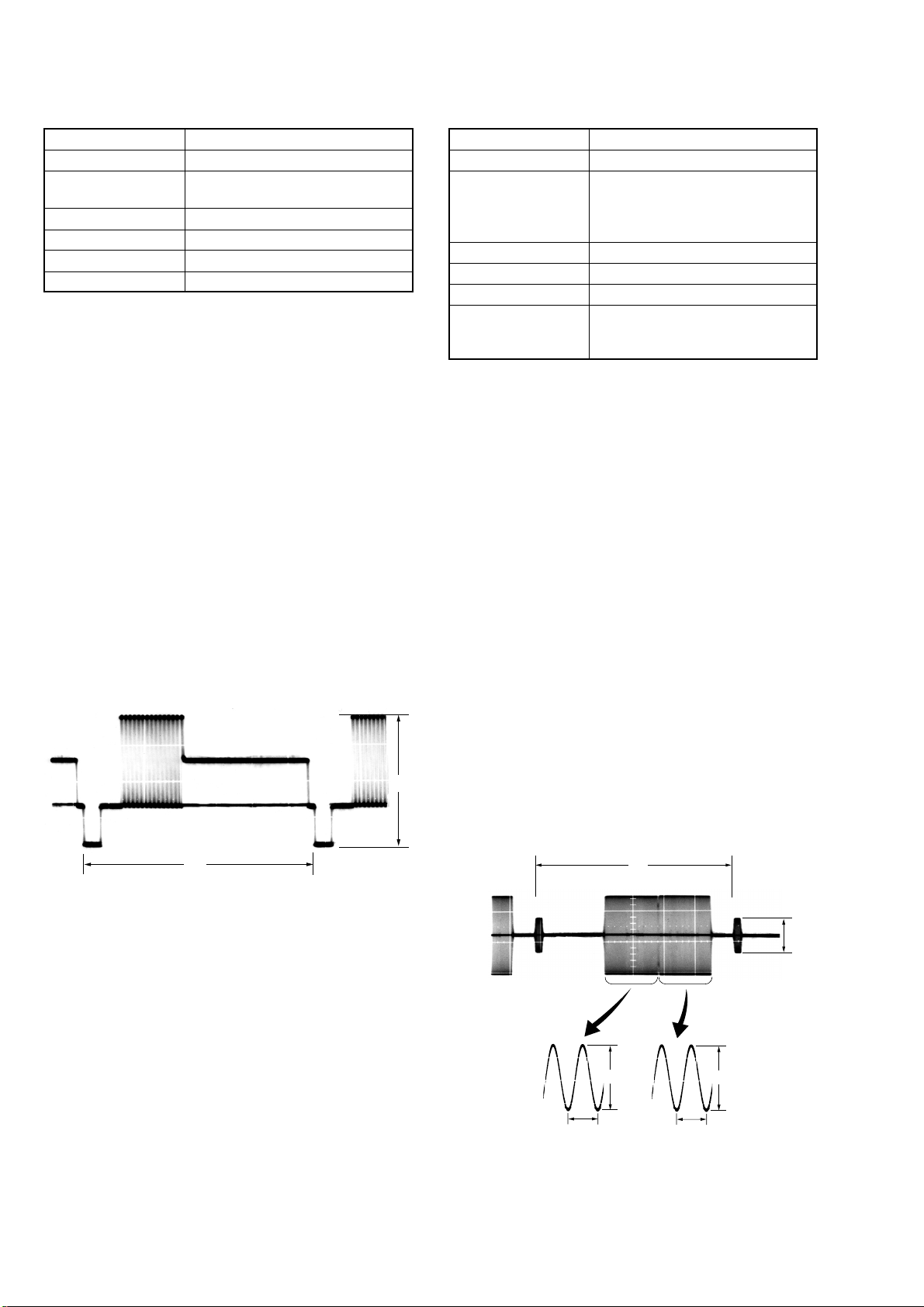
2. S-VIDEO OUT Y Level Adjustment
C
Mode VTR, Digital EE
Signal No signal
Measurement Point Y signal terminal of S VIDEO jack
(75 Ω terminated)
Measuring Instrument Oscilloscope
Adjustment Page C
Adjustment Address 25
Specified Value A = 1000 ± 14mVp-p
Adjusting method:
1) Select page: 0, address: 01, and set data: 01.
2) Select page: C, address: 48, set data: 06, and press the PAUSE
button of the adjustment remote commander. (VTR mode)
3) Select page: C, address: 56, set data: 00, and press the PAUSE
button of the adjustment remote commander. (digital EE mode)
4) Select page: 2, address: 35. After note down the data of this
address, set data: 01 to the address.
5) Select page: 3, address: 0C, set data: 02, and press the PAUSE
button of the adjustment remote commander.
6) Select page: C, address: 25, change the data and set the Y signal
level (A) to the specified value.
7) Press the PA USE b utton of the adjustment remote commander .
8) Select page: 3, address: 0C, set data: 00, and press the PAUSE
button of the adjustment remote commander.
9) Select page: 2, address: 35. and set the data that is noted down
at step 4).
10) Select page: C, address: 48, set data: 00, and press the PAUSE
button of the adjustment remote commander.
11) Select page: C, address: 56, set data: 08, and press the PAUSE
button of the adjustment remote commander.
12) Select page: 0, address: 01, and set data: 00.
A
3. S-VIDEO OUT Cr, Cb Level Adjustment
Mode VTR, Digital EE
Signal No signal
Measurement Point Chroma signal terminal of S VIDEO
jack (75 Ω terminated)
External trigger: Y signal terminal of
S VIDEO jack
Measuring Instrument Oscilloscope
Adjustment Page C
Adjustment Address 26, 27
Specified Value Cr level: A = 714 ± 14mVp-p
Cb level: B = 714 ± 14mVp-p
Burst level: C = 286 ± 16mVp-p
Adjusting method:
1) Select page: 0, address: 01, and set data: 01.
2) Select page: C, address: 48, set data: 06, and press the PAUSE
button of the adjustment remote commander. (VTR mode)
3) Select page: C, address: 56, set data: 00, and press the PAUSE
button of the adjustment remote commander. (digital EE mode)
4) Select page: 2, address: 35. After note down the data of this
address, set data: 01 to the address.
5) Select page: 3, address: 0C, set data: 02, and press the PAUSE
button of the adjustment remote commander.
6) Select page: C, address: 26, change the data to adjust the Cr
signal level (A) to the specified value.
7) Press the PA USE b utton of the adjustment remote commander .
8) Select page: C, address: 27, change the data to adjust the Cb
signal level (B) to the specified value.
9) Press the PA USE b utton of the adjustment remote commander .
10) Check that the burst signal level (C) is satisfied the specified
value.
11) Select page: 3, address: 0C, set data: 00, and press the PAUSE
button of the adjustment remote commander.
12) Select page: 2, address: 35, and set the data that is noted down
at step 4).
13) Select page: C, address: 48, set data: 00, and press the PAUSE
button of the adjustment remote commander.
14) Select page: C, address: 56, set data: 08, and press the PAUSE
button of the adjustment remote commander.
15) Select page: 0, address: 01, and set data: 00.
H
Fig. 4-6
H
A
0.28 µsec
0.28 µsec
B
Fig. 4-7
4-6
Page 30

4. VIDEO OUT Sync Level and Burst Level Check
Mode Digital EE
Signal No signal
Measurement Point Measurement Point Video out
terminal (75Ωterminated)
Measuring Instrument Oscilloscope
Specified Value Sync signal level: A = 286 ±20 mVp-p
Burst signal level: B = 286 ±30 mVp-p
Adjusting method:
1) Select page: 0, address: 01, and set data: 01.
2) Select page: C, address: 56, set data: 00, and press the PAUSE
button of the adjustment remote commander. (dig ital EE mode)
3) Check that the sync signal level (A) satisfies the specified value.
4) Check that the burst signal level (B) satisfies the specified value.
5) Select page: C, address: 56, set data: 08, and press the PAUSE
button of the adjustment remote commander.
6) Select page: 0, address: 01, and set data: 00.
B
A
H
Fig. 4-8
5. PLL Adjustment
Set the VCO center level of the video input circuit (IC102).
Mode Digital EE
Signal Color bar (VIDEO IN terminal input)
<3.579545 MHz ±10Hz>
Measurement Point Display data of page: 3, address: 04
Measuring Instrument Adjustment remote commander
Adjustment Page C
Adjustment Address AA
Specified Value 0A
Adjusting method:
1) Select page: 0, address: 01, and set data: 01.
2) Select page: C, address: 56, set data: 00, and press the PAUSE
button of the adjustment remote commander. (digital EE mode)
3) Select page: 3, address: 0C, set data: 80, and press the PAUSE
button of the adjustment remote commander.
4) Select page: C, address: AA, and set data: 00, and press the
PAUSE button.
5) Select page: 3, address: 04, and check. If the data is “0A” ,
proceed to step 8).
6) Select page: C, address: AA, add “10”(hexadecimal) to the data
and press the PAUSE button.
7) Select page: 3, address: 04, and check the data is “0A” . If not
repeat step 7).
8) Select page: 3, address: 0C, set data: 00, and press the PAUSE
button of the adjustment remote commander.
9) Select page: C, address: 56, set data: 08, and press the PAUSE
button of the adjustment remote commander.
10) Select page: 0, address: 01, and set data: 00.
4-7
Page 31

4-5. SER VICE MODE
ADJUSTMENT REMOTE COMMANDER
The adjustment remote commander is used for changing the
calculation coefficient in signal processing, EVR data, etc. The
adjustment remote commander performs bi-directional
communication with the unit using the remote commander signal
line (LANC). The resultant data of this bi-directional communication
is written in the non-volatile memory.
1. Using the adjustment remote commander
1) Connect the adjustment remote commander to the LANC
terminal.
2) Set the HOLD switch of the adjustment remote commander to
“HOLD” (SERVICE position). If it has been properly
connected, the LCD on the adjustment remote commander will
display as shown in Fig. 4-9.
Page
Data Address
Fig. 4-9
2. Precautions upon using
the adjustment remote commander
Mishandling of the adjustment remote commander may erase the
correct adjustment data at times. T o pre vent this, it is recommended
that all adjustment data be noted down before beginning adjustments
and new adjustment data after each adjustment.
3) Operate the adjustment remote commander as follows.
• Changing the page
The page increases when the EDIT SEARCH+ button is
pressed, and decreases when the EDIT SEARCH– button is
pressed. There are altogether 16 pages, from 0 to F.
Hexadecimal
notation
LCD Display
Decimal notation
conversion value
• Changing the address
The address increases when the FF (M) button is pressed,
and decreases when the REW (m) button is pressed. There
are altogether 256 addresses, from 00 to FF.
• Changing the data (Data setting)
The data increases when the PLAY (N) button is pressed,
and decreases when the STOP (x) button is pressed. There
are altogether 256 data, from 00 to FF.
• Writing the adjustment data
The PAUSE b utton must be pressed to write the adjustment
data (B, C, D, F page) in the nonvolatile memory. (The new
adjusting data will not be recorded in the nonvolatile memory
if this step is not performed.)
4) After completing all adjustments, turn off the main power
supply (8.4V) once.
0123456789ABCDEF
0123456789AbcdEF
0123456789101112131415
4-8E
Page 32
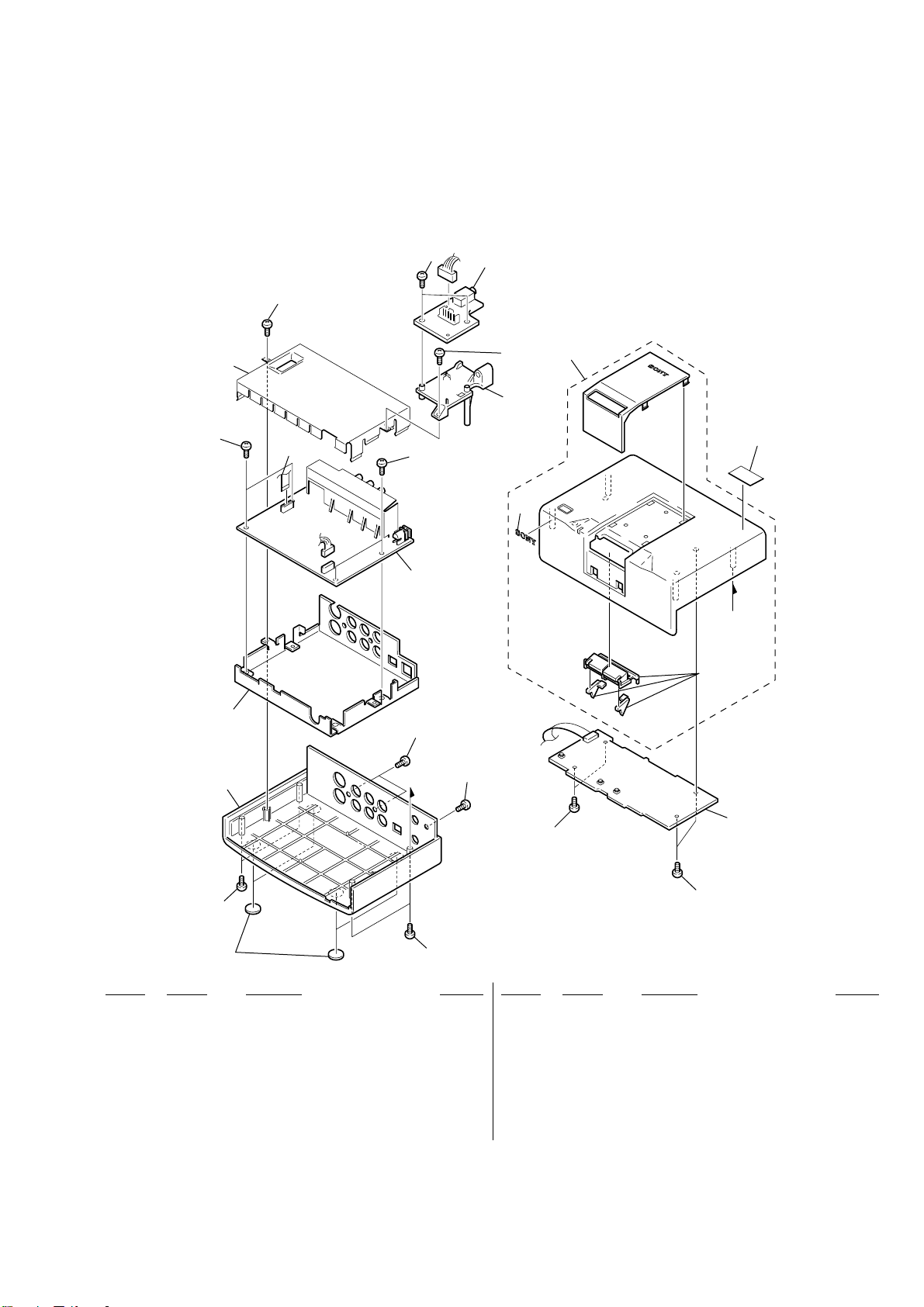
5-1. EXPLODED VIEWS
NOTE:
• -XX, -X mean standardized parts, so they may
have some differences from the original one.
• Items marked “*” are not stocked since they
are seldom required for routine service. Some
delay should be anticipated when ordering these
items.
SECTION 5
DVMC-DA2
REPAIR PARTS LIST
• The mechanical parts with no reference number
in the exploded views are not supplied.
8
13
8
7
8
9
14
1
6
1
16
10
4
not
supplied
3
12
2
12
11
8
5
15
Ref. No. Part No. Description Remarks Ref. No. Part No. Description Remarks
1 4-639-967-01 SCREW, 0 PLATE SPECIAL HEAD
2 X-4622-479-1 CABINET (LOWER) ASSY
* 3 4-639-053-11 SHIELD (LOWER)
4 A-8056-554-A IFX-52 BOARD, COMPLETE
5 4-982-491-01 SCREW (2X8) TAPPING
6 1-790-197-11 FFC(IF-SW)
* 7 4-639-054-02 SHIELD (UPPER)
8 4-641-086-01 TAPPING, PRECISION
5
9 A-8046-118-A CABINET (UPPER) BLOCK ASSY
10 4-942-636-21 EMBLEM (NO 3.5) SONY
11 A-8054-858-A SWX-22 BOARD, COMPLETE
12 7-685-647-74 +BV3X10
13 A-8056-556-A JK-02 BOARD, COMPLETE
* 14 4-644-562-01 STAY, RANK
15 4-641-233-01 FOOT, RUBBER
16 4-640-530-01 STICKER, I.LINK
8
5-1
Page 33

IFX-52
5-2. ELECTRICAL PARTS LIST
NOTE:
• Due to standardization, replacements in the
parts list may be different from the parts
specified in the diagrams or the components
used on the set.
• -XX, -X mean standardized parts, so they
may have some difference from the original
one.
• Items marked “*” are not stocked since they
are seldom required for routine service.
Some delay should be anticipated when
ordering these items.
Ref. No. Part No. Description Remarks Ref. No. Part No. Description Remarks
A-8056-554-A IFX-52 BOARD,COMPLETE
*********************
* 4-639-140-01 PLATE,JACK GROUND
< CAPACITOR >
C001 1-109-994-11 CERAMIC CHIP 2.2uF 10% 10V
C002 1-164-943-11 CERAMIC CHIP 0.01uF 10% 16V
C003 1-164-943-11 CERAMIC CHIP 0.01uF 10% 16V
C004 1-104-851-11 TANTALUM CHIP 10uF 20% 10V
C005 1-164-943-11 CERAMIC CHIP 0.01uF 10% 16V
C006 1-104-851-11 TANTALUM CHIP 10uF 20% 10V
C007 1-164-943-11 CERAMIC CHIP 0.01uF 10% 16V
C008 1-109-982-11 CERAMIC CHIP 1uF 10% 10V
C009 1-109-994-11 CERAMIC CHIP 2.2uF 10% 10V
C010 1-164-943-11 CERAMIC CHIP 0.01uF 10% 16V
C014 1-135-259-11 TANTALUM CHIP 10uF 20% 6.3V
C015 1-135-259-11 TANTALUM CHIP 10uF 20% 6.3V
C016 1-109-982-11 CERAMIC CHIP 1uF 10% 10V
C017 1-135-099-91 TANTALUM CHIP 2.2uF 20% 6.3V
C019 1-125-899-11 TANTALUM CHIP 220uF 20% 4V
C020 1-164-943-11 CERAMIC CHIP 0.01uF 10% 16V
C021 1-135-099-91 TANTALUM CHIP 2.2uF 20% 6.3V
C022 1-164-943-11 CERAMIC CHIP 0.01uF 10% 16V
C023 1-125-899-11 TANTALUM CHIP 220uF 20% 4V
C024 1-164-943-11 CERAMIC CHIP 0.01uF 10% 16V
C025 1-164-943-11 CERAMIC CHIP 0.01uF 10% 16V
C026 1-135-259-11 TANTALUM CHIP 10uF 20% 6.3V
C027 1-164-858-11 CERAMIC CHIP 22PF 5% 16V
C101 1-104-851-11 TANTALUM CHIP 10uF 20% 10V
C102 1-164-943-11 CERAMIC CHIP 0.01uF 10% 16V
C103 1-135-259-11 TANTALUM CHIP 10uF 20% 6.3V
C104 1-135-259-11 TANTALUM CHIP 10uF 20% 6.3V
C105 1-164-943-11 CERAMIC CHIP 0.01uF 10% 16V
C106 1-119-750-11 TANTALUM CHIP 22uF 20% 6.3V
C107 1-164-856-81 CERAMIC CHIP 18PF 5% 16V
C108 1-109-982-11 CERAMIC CHIP 1uF 10% 10V
C109 1-164-874-11 CERAMIC CHIP 100PF 5% 16V
C110 1-164-943-11 CERAMIC CHIP 0.01uF 10% 16V
C111 1-164-943-11 CERAMIC CHIP 0.01uF 10% 16V
C112 1-135-210-11 TANTALUM CHIP 4.7uF 20% 10V
C113 1-135-210-11 TANTALUM CHIP 4.7uF 20% 10V
C115 1-164-874-11 CERAMIC CHIP 100PF 5% 16V
C116 1-164-937-11 CERAMIC CHIP 0.001uF 10% 16V
C117 1-109-982-11 CERAMIC CHIP 1uF 10% 10V
C118 1-164-943-11 CERAMIC CHIP 0.01uF 10% 16V
• CAPACITORS:
uF: µF
• RESISTORS
All resistors are in ohms.
METAL: metal-film resistor
METAL OXIDE: Metal Oxide-film resistor
F: nonflammable
• COILS
uH: µH
When indicating parts by reference number,
please include the board name.
C119 1-135-259-11 TANTALUM CHIP 10uF 20% 6.3V
C120 1-164-943-11 CERAMIC CHIP 0.01uF 10% 16V
C121 1-164-943-11 CERAMIC CHIP 0.01uF 10% 16V
C123 1-164-874-11 CERAMIC CHIP 100PF 5% 16V
C124 1-164-943-11 CERAMIC CHIP 0.01uF 10% 16V
C125 1-164-856-81 CERAMIC CHIP 18PF 5% 16V
C126 1-164-943-11 CERAMIC CHIP 0.01uF 10% 16V
C127 1-164-943-11 CERAMIC CHIP 0.01uF 10% 16V
C128 1-125-777-11 CERAMIC CHIP 0.1uF 10% 10V
C129 1-164-943-11 CERAMIC CHIP 0.01uF 10% 16V
C130 1-125-777-11 CERAMIC CHIP 0.1uF 10% 10V
C131 1-164-943-11 CERAMIC CHIP 0.01uF 10% 16V
C132 1-164-943-11 CERAMIC CHIP 0.01uF 10% 16V
C133 1-164-943-11 CERAMIC CHIP 0.01uF 10% 16V
C134 1-125-777-11 CERAMIC CHIP 0.1uF 10% 10V
C135 1-125-777-11 CERAMIC CHIP 0.1uF 10% 10V
C136 1-125-777-11 CERAMIC CHIP 0.1uF 10% 10V
C137 1-135-259-11 TANTALUM CHIP 10uF 20% 6.3V
C203 1-135-259-11 TANTALUM CHIP 10uF 20% 6.3V
C204 1-135-259-11 TANTALUM CHIP 10uF 20% 6.3V
C207 1-107-823-11 CERAMIC CHIP 0.47uF 10% 16V
C208 1-107-823-11 CERAMIC CHIP 0.47uF 10% 16V
C209 1-164-943-11 CERAMIC CHIP 0.01uF 10% 16V
C210 1-135-259-11 TANTALUM CHIP 10uF 20% 6.3V
C211 1-135-259-11 TANTALUM CHIP 10uF 20% 6.3V
C215 1-107-686-11 TANTALUM CHIP 4.7uF 20% 16V
C217 1-135-091-00 TANTALUM CHIP 1uF 20% 16V
C219 1-135-259-11 TANTALUM CHIP 10uF 20% 6.3V
C221 1-164-943-11 CERAMIC CHIP 0.01uF 10% 16V
C222 1-109-982-11 CERAMIC CHIP 1uF 10% 10V
C225 1-135-099-91 TANTALUM CHIP 2.2uF 20% 6.3V
C226 1-109-982-11 CERAMIC CHIP 1uF 10% 10V
C229 1-107-823-11 CERAMIC CHIP 0.47uF 10% 16V
C230 1-135-259-11 TANTALUM CHIP 10uF 20% 6.3V
C231 1-164-245-11 CERAMIC CHIP 0.015uF 10% 25V
C232 1-164-245-11 CERAMIC CHIP 0.015uF 10% 25V
C233 1-164-943-11 CERAMIC CHIP 0.01uF 10% 16V
C234 1-164-943-11 CERAMIC CHIP 0.01uF 10% 16V
C235 1-164-943-11 CERAMIC CHIP 0.01uF 10% 16V
C236 1-135-259-11 TANTALUM CHIP 10uF 20% 6.3V
C237 1-135-259-11 TANTALUM CHIP 10uF 20% 6.3V
C238 1-135-259-11 TANTALUM CHIP 10uF 20% 6.3V
C239 1-164-943-11 CERAMIC CHIP 0.01uF 10% 16V
C240 1-135-259-11 TANTALUM CHIP 10uF 20% 6.3V
C242 1-164-943-11 CERAMIC CHIP 0.01uF 10% 16V
• SEMICONDUCTORS
In each case, u: µ, for example:
uA...: µA... , uPA... , µPA... ,
uPB... , µPB... , uPC... , µPC... ,
uPD..., µPD...
The components identified by mark 0 or
dotted line with mark 0 are critical for safety.
Replace only with part number specified.
Les composants identifiés par une marque
0 sont critiques pour la sécurité.
Ne les remplacer que par une pièce portant
le numéro spécifié.
5-2
Page 34

IFX-52
Ref. No. Part No. Description Remarks Ref. No. Part No. Description Remarks
C243 1-164-943-11 CERAMIC CHIP 0.01uF 10% 16V
C244 1-135-259-11 TANTALUM CHIP 10uF 20% 6.3V
C245 1-135-259-11 TANTALUM CHIP 10uF 20% 6.3V
C247 1-164-943-11 CERAMIC CHIP 0.01uF 10% 16V
C248 1-125-777-11 CERAMIC CHIP 0.1uF 10% 10V
C362 1-164-227-11 CERAMIC CHIP 0.022uF 10% 25V
C401 1-164-943-11 CERAMIC CHIP 0.01uF 10% 16V
C402 1-164-943-11 CERAMIC CHIP 0.01uF 10% 16V
C403 1-125-899-11 TANTALUM CHIP 220uF 20% 4V
C404 1-164-943-11 CERAMIC CHIP 0.01uF 10% 16V
C249 1-125-777-11 CERAMIC CHIP 0.1uF 10% 10V
C250 1-125-777-11 CERAMIC CHIP 0.1uF 10% 10V
C301 1-107-826-91 CERAMIC CHIP 0.1uF 10% 16V
C302 1-162-970-11 CERAMIC CHIP 0.01uF 10% 25V
C303 1-109-982-11 CERAMIC CHIP 1uF 10% 10V
C304 1-109-982-11 CERAMIC CHIP 1uF 10% 10V
C305 1-125-838-91 CERAMIC CHIP 2.2uF 10% 6.3V
C306 1-162-964-11 CERAMIC CHIP 0.001uF 10% 50V
C307 1-162-964-11 CERAMIC CHIP 0.001uF 10% 50V
C308 1-109-982-11 CERAMIC CHIP 1uF 10% 10V
C309 1-164-935-11 CERAMIC CHIP 470PF 10% 16V
C310 1-162-927-11 CERAMIC CHIP 100PF 5% 50V
C311 1-164-935-11 CERAMIC CHIP 470PF 10% 16V
C312 1-164-935-11 CERAMIC CHIP 470PF 10% 16V
C313 1-104-913-11 TANTALUM CHIP 10uF 20% 16V
C314 1-104-913-11 TANTALUM CHIP 10uF 20% 16V
C315 1-163-809-11 CERAMIC CHIP 0.047uF 10% 25V
C319 1-162-964-11 CERAMIC CHIP 0.001uF 10% 50V
C322 1-162-966-11 CERAMIC CHIP 0.0022uF 10% 50V
C324 1-109-982-11 CERAMIC CHIP 1uF 10% 10V
C329 1-162-966-11 CERAMIC CHIP 0.0022uF 10% 50V
C330 1-162-970-11 CERAMIC CHIP 0.01uF 10% 25V
C331 1-162-970-11 CERAMIC CHIP 0.01uF 10% 25V
C332 1-115-566-11 CERAMIC CHIP 4.7uF 10% 10V
C333 1-115-566-11 CERAMIC CHIP 4.7uF 10% 10V
C405 1-162-970-11 CERAMIC CHIP 0.01uF 10% 25V
C406 1-109-982-11 CERAMIC CHIP 1uF 10% 10V
C407 1-164-943-11 CERAMIC CHIP 0.01uF 10% 16V
C501 1-135-099-91 TANTALUM CHIP 2.2uF 20% 6.3V
C502 1-165-176-11 CERAMIC CHIP 0.047uF 10% 16V
C503 1-164-937-11 CERAMIC CHIP 0.001uF 10% 16V
C504 1-135-259-11 TANTALUM CHIP 10uF 20% 6.3V
C505 1-164-943-11 CERAMIC CHIP 0.01uF 10% 16V
C506 1-135-259-11 TANTALUM CHIP 10uF 20% 6.3V
C507 1-135-259-11 TANTALUM CHIP 10uF 20% 6.3V
C508 1-164-937-11 CERAMIC CHIP 0.001uF 10% 16V
C509 1-164-937-11 CERAMIC CHIP 0.001uF 10% 16V
C510 1-218-945-11 RES,CHIP 220 5% 1/16W
C511 1-164-852-11 CERAMIC CHIP 12PF 5% 16V
C512 1-164-852-11 CERAMIC CHIP 12PF 5% 16V
C513 1-164-943-11 CERAMIC CHIP 0.01uF 10% 16V
C514 1-164-943-11 CERAMIC CHIP 0.01uF 10% 16V
C515 1-135-259-11 TANTALUM CHIP 10uF 20% 6.3V
C516 1-164-943-11 CERAMIC CHIP 0.01uF 10% 16V
C517 1-164-943-11 CERAMIC CHIP 0.01uF 10% 16V
C519 1-125-777-11 CERAMIC CHIP 0.1uF 10% 10V
C521 1-164-943-11 CERAMIC CHIP 0.01uF 10% 16V
C522 1-109-982-11 CERAMIC CHIP 1uF 10% 10V
C523 1-164-882-11 CERAMIC CHIP 220PF 5% 16V
C601 1-164-937-11 CERAMIC CHIP 0.001uF 10% 16V
C334 1-115-566-11 CERAMIC CHIP 4.7uF 10% 10V
C335 1-115-566-11 CERAMIC CHIP 4.7uF 10% 10V
C336 1-115-566-11 CERAMIC CHIP 4.7uF 10% 10V
C337 1-115-566-11 CERAMIC CHIP 4.7uF 10% 10V
C338 1-135-259-11 TANTALUM CHIP 10uF 20% 6.3V
C339 1-135-259-11 TANTALUM CHIP 10uF 20% 6.3V
C340 1-135-259-11 TANTALUM CHIP 10uF 20% 6.3V
C341 1-104-851-11 TANTALUM CHIP 10uF 20% 10V
C342 1-135-259-11 TANTALUM CHIP 10uF 20% 6.3V
C343 1-104-851-11 TANTALUM CHIP 10uF 20% 10V
C344 1-107-819-11 CERAMIC CHIP 0.022uF 10% 16V
C345 1-107-819-11 CERAMIC CHIP 0.022uF 10% 16V
C346 1-104-851-11 TANTALUM CHIP 10uF 20% 10V
C347 1-135-259-11 TANTALUM CHIP 10uF 20% 6.3V
C348 1-164-943-11 CERAMIC CHIP 0.01uF 10% 16V
C349 1-135-091-00 TANTALUM CHIP 1uF 20% 16V
C350 1-135-091-00 TANTALUM CHIP 1uF 20% 16V
C351 1-164-943-11 CERAMIC CHIP 0.01uF 10% 16V
C352 1-164-943-11 CERAMIC CHIP 0.01uF 10% 16V
C353 1-135-091-00 TANTALUM CHIP 1uF 20% 16V
C355 1-115-566-11 CERAMIC CHIP 4.7uF 10% 10V
C356 1-115-566-11 CERAMIC CHIP 4.7uF 10% 10V
C357 1-115-566-11 CERAMIC CHIP 4.7uF 10% 10V
C359 1-135-259-11 TANTALUM CHIP 10uF 20% 6.3V
C361 1-110-563-11 CERAMIC CHIP 0.068uF 10% 16V
C602 1-164-852-11 CERAMIC CHIP 12PF 5% 16V
C603 1-164-852-11 CERAMIC CHIP 12PF 5% 16V
C604 1-109-982-11 CERAMIC CHIP 1uF 10% 10V
C605 1-218-945-11 RES,CHIP 220 5% 1/16W
C606 1-218-945-11 RES,CHIP 220 5% 1/16W
C701 1-107-820-11 CERAMIC CHIP 0.1uF 16V
C702 1-107-820-11 CERAMIC CHIP 0.1uF 16V
C703 1-107-820-11 CERAMIC CHIP 0.1uF 16V
C704 1-104-847-11 TANTALUM CHIP 22uF 20% 4V
C705 1-104-851-11 TANTALUM CHIP 10uF 20% 10V
C706 1-164-943-11 CERAMIC CHIP 0.01uF 10% 16V
C707 1-164-943-11 CERAMIC CHIP 0.01uF 10% 16V
C708 1-164-943-11 CERAMIC CHIP 0.01uF 10% 16V
C709 1-107-819-11 CERAMIC CHIP 0.022uF 10% 16V
C712 1-107-820-11 CERAMIC CHIP 0.1uF 16V
C713 1-164-943-11 CERAMIC CHIP 0.01uF 10% 16V
C714 1-107-820-11 CERAMIC CHIP 0.1uF 16V
C715 1-107-820-11 CERAMIC CHIP 0.1uF 16V
C801 1-164-943-11 CERAMIC CHIP 0.01uF 10% 16V
< CONNECTOR >
CN701 1-770-305-11 CONNECTOR,FFC/FPC 10P
CN801 1-779-523-11 CONNECTOR,SQUARE TYPE (INDI) 4P
(DV IN/OUT)
CN802 1-573-290-21 PIN CONNECTOR (1.5MM) (SMD) 4P
CN905 1-750-321-41 CONNECTOR,BOARD TO BOARD 20P
5-3
Page 35

IFX-52
Ref. No. Part No. Description Remarks Ref. No. Part No. Description Remarks
< DIODE >
D101 8-719-071-32 DIODE HVC350BTRF
D102 8-719-071-32 DIODE HVC350BTRF
D302 8-719-066-34 DIODE RB461F-T106
D303 8-719-066-34 DIODE RB461F-T106
D304 8-719-066-16 DIODE RB491D-T146
FL501 1-234-177-21 FERRITE,CHIP EMI
FL503 1-234-177-21 FERRITE,CHIP EMI
FL504 1-234-177-21 FERRITE,CHIP EMI
FL505 1-234-177-21 FERRITE,CHIP EMI
FL601 1-234-177-21 FERRITE,CHIP EMI
FL701 1-234-177-21 FERRITE,CHIP EMI
D501 8-719-055-86 DIODE KV1470TL1-3
D701 8-719-421-27 DIODE MA728-TX
D702 8-719-056-23 DIODE MA2S111-(K8).SO
D703 8-719-064-61 DIODE 01BZA8.2(TE85L)
D705 8-719-064-61 DIODE 01BZA8.2(TE85L)
D706 8-719-064-61 DIODE 01BZA8.2(TE85L)
D707 8-719-064-61 DIODE 01BZA8.2(TE85L)
D801 8-719-064-61 DIODE 01BZA8.2(TE85L)
D802 8-719-064-61 DIODE 01BZA8.2(TE85L)
< FUSE >
0F301 1-533-760-21 FUSE (SMD)(1.4A)
< FERRITE BEAD >
* FB301 1-500-449-21 BEAD,FERRITE 0UH
* FB302 1-500-449-21 BEAD,FERRITE 0UH
FB739 1-414-555-21 FERRITE,EMI 0UH
FB740 1-414-555-21 FERRITE,EMI 0UH
FB741 1-414-555-21 FERRITE,EMI 0UH
FB742 1-414-555-21 FERRITE,EMI 0UH
FB743 1-414-555-21 FERRITE,EMI 0UH
FB744 1-414-555-21 FERRITE,EMI 0UH
* FB746 1-469-092-11 FERRITE,EMI 0UH
* FB747 1-469-092-11 FERRITE,EMI 0UH
FB748 1-414-555-21 FERRITE,EMI 0UH
FB801 1-469-108-21 FERRITE,EMI 0UH
FB802 1-469-108-21 FERRITE,EMI 0UH
FB803 1-469-108-21 FERRITE,EMI 0UH
FB804 1-469-108-21 FERRITE,EMI 0UH
FB805 1-469-311-22 BEAD,FERRITE 0UH
FB806 1-500-113-22 BEAD,FERRITE 0UH
FB807 1-469-311-22 BEAD,FERRITE 0UH
FB808 1-469-311-22 BEAD,FERRITE 0UH
FB809 1-469-311-22 BEAD,FERRITE 0UH
FB810 1-469-311-22 BEAD,FERRITE 0UH
FB811 1-469-311-22 BEAD,FERRITE 0UH
FB812 1-500-113-22 BEAD,FERRITE 0UH
FB813 1-500-113-22 BEAD,FERRITE 0UH
FB814 1-500-113-22 BEAD,FERRITE 0UH
FB815 1-500-113-22 BEAD,FERRITE 0UH
FB816 1-469-311-22 BEAD,FERRITE 0UH
FB817 1-469-311-22 BEAD,FERRITE 0UH
FB818 1-469-311-22 BEAD,FERRITE 0UH
FB819 1-469-311-22 BEAD,FERRITE 0UH
< FILTER >
FL101 1-234-177-21 FERRITE,CHIP EMI
FL301 1-233-893-11 FERRITE,CHIP EMI
FL401 1-234-177-21 FERRITE,CHIP EMI
FL402 1-234-177-21 FERRITE,CHIP EMI
FL404 1-234-177-21 FERRITE,CHIP EMI
< IC >
IC001 8-759-534-25 IC AN2222FBQ-EB
IC002 8-759-432-78 IC MM1111XFBE
IC101 8-759-430-57 IC M62367GP-75ED
IC102 8-759-579-81 IC SC371053AFTAEB
IC201 8-759-583-66 IC AN2902FHQBEB
IC202 8-759-524-60 IC AK4512-VF-E2
IC301 8-759-060-93 IC MB3785APFV-G-BND-ER
IC401 8-759-584-66 IC M65511AWG-600D
IC501 8-759-584-36 IC HG73C050BPTL
IC502 8-752-394-00 IC CXD3129R-T6
IC503 8-759-566-52 IC SN104266PN-TEB
IC601 8-759-653-34 IC MB91191RPFF-G-151-BND-ER
IC602 8-759-445-94 IC AK6480AM-E2
IC701 8-759-424-79 IC S-8423YFS-T2
IC702 8-759-536-45 IC TL1596CPW-ELM2000
IC703 8-759-653-33 IC S579195PZ-TEB
IC704 8-759-524-29 IC TC74VHC257FT(EL)
< JACK >
J301 1-770-443-11 JACK,DC(POLARITY UNIFIED TYPE)(DC IN 6V)
J802 1-785-511-11 AV JACK(S-VIDEO/VIDEO/AUDIO)
< INDUCTOR >
L001 1-414-754-11 INDUCTOR 10uH
L002 1-414-754-11 INDUCTOR 10uH
L101 1-414-754-11 INDUCTOR 10uH
L102 1-414-757-11 INDUCTOR 100uH
L103 1-412-957-11 INDUCTOR,SMALL TYPE 33uH
L104 1-412-943-81 INDUCTOR 2.2uH
L105 1-412-957-11 INDUCTOR,SMALL TYPE 33uH
L106 1-414-754-11 INDUCTOR 10uH
L201 1-414-754-11 INDUCTOR 10uH
L202 1-414-754-11 INDUCTOR 10uH
L203 1-414-754-11 INDUCTOR 10uH
L305 1-416-345-11 COIL,CHOKE 22uH
L306 1-416-345-11 COIL,CHOKE 22uH
L307 1-416-345-11 COIL,CHOKE 22uH
L308 1-412-056-11 INDUCTOR(SMD) 4.7uH
L309 1-412-056-11 INDUCTOR(SMD) 4.7uH
L310 1-412-056-11 INDUCTOR(SMD) 4.7uH
L311 1-412-056-11 INDUCTOR(SMD) 4.7uH
L312 1-412-056-11 INDUCTOR(SMD) 4.7uH
L313 1-412-056-11 INDUCTOR(SMD) 4.7uH
L314 1-412-056-11 INDUCTOR(SMD) 4.7uH
L315 1-412-056-11 INDUCTOR(SMD) 4.7uH
L316 1-412-056-11 INDUCTOR(SMD) 4.7uH
L401 1-414-757-11 INDUCTOR 100uH
* L402 1-414-482-21 INDUCTOR CHIP 82NH
5-4
Note :
The components identified by
mark 0 or dotted line with mark
0 are critical for safety.
Replace only with part number
specified.
Note :
Les composants identifiés par
une marque 0 sont critiques
pour la sécurité.
Ne les remplacer que par une
pièce portant le numéro spécifié.
Page 36

IFX-52
Ref. No. Part No. Description Remarks Ref. No. Part No. Description Remarks
L403 1-414-757-11 INDUCTOR 100uH
L501 1-414-754-11 INDUCTOR 10uH
L502 1-414-754-11 INDUCTOR 10uH
L503 1-414-754-11 INDUCTOR 10uH
L504 1-412-941-11 INDUCTOR 1.5uH
R007 1-218-953-11 RES,CHIP 1K 5% 1/16W
R008 1-218-990-11 CONDUCTOR,CHIP 0
R009 1-218-990-11 CONDUCTOR,CHIP 0
R010 1-218-969-11 RES,CHIP 22K 5% 1/16W
R011 1-218-941-11 RES,CHIP 100 5% 1/16W
L505 1-414-754-11 INDUCTOR 10uH
L601 1-414-754-11 INDUCTOR 10uH
L701 1-414-754-11 INDUCTOR 10uH
< LINE FILTER >
LF301 1-411-957-11 FILTER,COMMON MODE
< IC LINK >
0PS701 1-576-122-21 LINK,IC 0.4A
< TRANSISTOR >
Q003 8-729-042-70 TRANSISTOR UN9211J-(K8).SO
Q004 8-729-042-28 TRANSISTOR 2SD2216J-QR(K8).SO
Q101 8-729-807-94 TRANSISTOR 2SB1295-UL5-TB
Q102 8-729-042-73 TRANSISTOR UN9215J-(K8).SO
Q103 8-729-042-28 TRANSISTOR 2SD2216J-QR(K8).SO
Q104 8-729-042-26 TRANSISTOR 2SB1462J-QR(K8).SO
Q105 8-729-042-28 TRANSISTOR 2SD2216J-QR(K8).SO
Q106 8-729-042-28 TRANSISTOR 2SD2216J-QR(K8).SO
Q107 8-729-042-28 TRANSISTOR 2SD2216J-QR(K8).SO
Q108 8-729-042-28 TRANSISTOR 2SD2216J-QR(K8).SO
Q109 8-729-042-26 TRANSISTOR 2SB1462J-QR(K8).SO
Q110 8-729-807-94 TRANSISTOR 2SB1295-UL5-TB
Q201 8-729-042-32 TRANSISTOR UN9113J-(K8).SO
Q202 8-729-042-69 TRANSISTOR UN9210J-(K8).SO
Q203 8-729-042-69 TRANSISTOR UN9210J-(K8).SO
Q205 8-729-041-23 TRANSISTOR NDS356AP
Q206 8-729-042-31 TRANSISTOR UN9213J-(K8).SO
Q207 8-729-041-23 TRANSISTOR NDS356AP
Q208 8-729-042-31 TRANSISTOR UN9213J-(K8).SO
Q209 8-729-042-70 TRANSISTOR UN9211J-(K8).SO
Q302 8-729-043-94 TRANSISTOR CPH3106-PM-TL
Q303 8-729-043-94 TRANSISTOR CPH3106-PM-TL
Q304 8-729-043-94 TRANSISTOR CPH3106-PM-TL
Q305 8-729-041-23 TRANSISTOR NDS356AP
Q306 8-729-042-31 TRANSISTOR UN9213J-(K8).SO
Q307 8-729-042-31 TRANSISTOR UN9213J-(K8).SO
Q308 8-729-041-23 TRANSISTOR NDS356AP
Q701 8-729-042-58 TRANSISTOR UN9111J-(K8).SO
Q702 8-729-042-70 TRANSISTOR UN9211J-(K8).SO
Q703 8-729-042-70 TRANSISTOR UN9211J-(K8).SO
Q704 8-729-042-70 TRANSISTOR UN9211J-(K8).SO
Q705 8-729-042-70 TRANSISTOR UN9211J-(K8).SO
Q951 8-729-042-72 TRANSISTOR UN9214J-(K8).SO
R012 1-218-941-11 RES,CHIP 100 5% 1/16W
R013 1-218-941-11 RES,CHIP 100 5% 1/16W
R014 1-218-953-11 RES,CHIP 1K 5% 1/16W
R015 1-218-953-11 RES,CHIP 1K 5% 1/16W
R016 1-218-965-11 RES,CHIP 10K 5% 1/16W
R017 1-218-939-11 RES,CHIP 68 5% 1/16W
R018 1-218-939-11 RES,CHIP 68 5% 1/16W
R019 1-218-939-11 RES,CHIP 68 5% 1/16W
R020 1-218-981-11 RES,CHIP 220K 5% 1/16W
R021 1-218-941-11 RES,CHIP 100 5% 1/16W
R023 1-218-961-11 RES,CHIP 4.7K 5% 1/16W
R024 1-218-961-11 RES,CHIP 4.7K 5% 1/16W
R028 1-218-953-11 RES,CHIP 1K 5% 1/16W
R029 1-218-957-11 RES,CHIP 2.2K 5% 1/16W
R030 1-218-939-11 RES,CHIP 68 5% 1/16W
R031 1-218-989-11 RES,CHIP 1M 5% 1/16W
R101 1-218-973-11 RES,CHIP 47K 5% 1/16W
R102 1-218-965-11 RES,CHIP 10K 5% 1/16W
R103 1-218-953-11 RES,CHIP 1K 5% 1/16W
R104 1-218-959-11 RES,CHIP 3.3K 5% 1/16W
R105 1-218-957-11 RES,CHIP 2.2K 5% 1/16W
R106 1-218-953-11 RES,CHIP 1K 5% 1/16W
R107 1-218-979-11 RES,CHIP 150K 5% 1/16W
R108 1-218-959-11 RES,CHIP 3.3K 5% 1/16W
R109 1-218-965-11 RES,CHIP 10K 5% 1/16W
R110 1-218-953-11 RES,CHIP 1K 5% 1/16W
R111 1-218-990-11 CONDUCTOR,CHIP 0
R112 1-218-953-11 RES,CHIP 1K 5% 1/16W
R113 1-218-977-11 RES,CHIP 100K 5% 1/16W
R114 1-218-989-11 RES,CHIP 1M 5% 1/16W
R115 1-218-977-11 RES,CHIP 100K 5% 1/16W
R116 1-218-977-11 RES,CHIP 100K 5% 1/16W
R117 1-218-965-11 RES,CHIP 10K 5% 1/16W
R118 1-218-965-11 RES,CHIP 10K 5% 1/16W
R119 1-218-977-11 RES,CHIP 100K 5% 1/16W
R120 1-218-950-11 RES,CHIP 560 5% 1/16W
R121 1-216-864-11 RES,CHIP 0 5% 1/16W
R122 1-218-953-11 RES,CHIP 1K 5% 1/16W
R123 1-218-952-11 RES,CHIP 820 5% 1/16W
R124 1-218-965-11 RES,CHIP 10K 5% 1/16W
R127 1-218-990-11 CONDUCTOR,CHIP 0
R128 1-218-990-11 CONDUCTOR,CHIP 0
R201 1-218-953-11 RES,CHIP 1K 5% 1/16W
R202 1-218-953-11 RES,CHIP 1K 5% 1/16W
R203 1-218-973-11 RES,CHIP 47K 5% 1/16W
< RESISTOR >
R002 1-218-965-11 RES,CHIP 10K 5% 1/16W
R003 1-218-941-11 RES,CHIP 100 5% 1/16W
R004 1-218-969-11 RES,CHIP 22K 5% 1/16W
R005 1-218-953-11 RES,CHIP 1K 5% 1/16W
R006 1-218-990-11 CONDUCTOR,CHIP 0
R204 1-218-973-11 RES,CHIP 47K 5% 1/16W
R205 1-218-965-11 RES,CHIP 10K 5% 1/16W
R206 1-218-965-11 RES,CHIP 10K 5% 1/16W
R207 1-218-973-11 RES,CHIP 47K 5% 1/16W
R209 1-218-990-11 CONDUCTOR,CHIP 0
5-5
Note :
The components identified by
mark 0 or dotted line with mark
0 are critical for safety.
Replace only with part number
specified.
Note :
Les composants identifiés par
une marque 0 sont critiques
pour la sécurité.
Ne les remplacer que par une
pièce portant le numéro spécifié.
Page 37

IFX-52
Ref. No. Part No. Description Remarks Ref. No. Part No. Description Remarks
R210 1-218-941-11 RES,CHIP 100 5% 1/16W
R212 1-218-949-11 RES,CHIP 470 5% 1/16W
R213 1-218-941-11 RES,CHIP 100 5% 1/16W
R214 1-218-949-11 RES,CHIP 470 5% 1/16W
R215 1-218-990-11 CONDUCTOR,CHIP 0
R370 1-216-295-91 CONDUCTOR,CHIP 0
R401 1-216-864-11 RES,CHIP 0 5% 1/16W
R402 1-218-977-11 RES,CHIP 100K 5% 1/16W
R403 1-218-959-11 RES,CHIP 3.3K 5% 1/16W
R404 1-218-959-11 RES,CHIP 3.3K 5% 1/16W
R216 1-218-990-11 CONDUCTOR,CHIP 0
R217 1-218-990-11 CONDUCTOR,CHIP 0
R219 1-218-989-11 RES,CHIP 1M 5% 1/16W
R220 1-218-979-11 RES,CHIP 150K 5% 1/16W
R221 1-218-989-11 RES,CHIP 1M 5% 1/16W
R222 1-218-979-11 RES,CHIP 150K 5% 1/16W
R223 1-218-990-11 CONDUCTOR,CHIP 0
R301 1-208-903-81 RES,CHIP 4.7K 0.50% 1/16W
R302 1-208-903-81 RES,CHIP 4.7K 0.50% 1/16W
R303 1-208-903-81 RES,CHIP 4.7K 0.50% 1/16W
R304 1-208-903-81 RES,CHIP 4.7K 0.50% 1/16W
R305 1-218-979-11 RES,CHIP 150K 5% 1/16W
R306 1-218-981-11 RES,CHIP 220K 5% 1/16W
R307 1-208-895-81 RES,CHIP 2.2K 0.50% 1/16W
R308 1-218-981-11 RES,CHIP 220K 5% 1/16W
R309 1-218-957-11 RES,CHIP 2.2K 5% 1/16W
R310 1-218-957-11 RES,CHIP 2.2K 5% 1/16W
R312 1-208-905-81 RES,CHIP 5.6K 0.50% 1/16W
R313 1-218-974-11 RES,CHIP 56K 5% 1/16W
R315 1-218-955-11 RES,CHIP 1.5K 5% 1/16W
R316 1-218-951-11 RES,CHIP 680 5% 1/16W
R317 1-208-899-81 RES,CHIP 3.3K 0.50% 1/16W
R318 1-208-903-81 RES,CHIP 4.7K 0.50% 1/16W
R319 1-216-023-00 RES,CHIP 82 5% 1/10W
R320 1-218-969-11 RES,CHIP 22K 5% 1/16W
R405 1-216-864-11 RES,CHIP 0 5% 1/16W
R406 1-218-990-11 CONDUCTOR,CHIP 0
R407 1-218-965-11 RES,CHIP 10K 5% 1/16W
R408 1-218-965-11 RES,CHIP 10K 5% 1/16W
R409 1-218-965-11 RES,CHIP 10K 5% 1/16W
R410 1-218-951-11 RES,CHIP 680 5% 1/16W
R411 1-218-947-11 RES,CHIP 330 5% 1/16W
R416 1-218-990-11 CONDUCTOR,CHIP 0
R417 1-218-965-11 RES,CHIP 10K 5% 1/16W
R418 1-218-965-11 RES,CHIP 10K 5% 1/16W
R419 1-218-965-11 RES,CHIP 10K 5% 1/16W
R501 1-218-937-11 RES,CHIP 47 5% 1/16W
R502 1-218-961-11 RES,CHIP 4.7K 5% 1/16W
R503 1-218-947-11 RES,CHIP 330 5% 1/16W
R504 1-218-965-11 RES,CHIP 10K 5% 1/16W
R505 1-218-965-11 RES,CHIP 10K 5% 1/16W
R506 1-218-990-11 CONDUCTOR,CHIP 0
R507 1-218-990-11 CONDUCTOR,CHIP 0
R508 1-218-990-11 CONDUCTOR,CHIP 0
R509 1-218-990-11 CONDUCTOR,CHIP 0
R510 1-218-950-11 RES,CHIP 560 5% 1/16W
R512 1-218-990-11 CONDUCTOR,CHIP 0
R513 1-218-990-11 CONDUCTOR,CHIP 0
R514 1-218-990-11 CONDUCTOR,CHIP 0
R516 1-218-990-11 CONDUCTOR,CHIP 0
R321 1-216-023-00 RES,CHIP 82 5% 1/10W
R322 1-216-023-00 RES,CHIP 82 5% 1/10W
R325 1-218-967-11 RES,CHIP 15K 5% 1/16W
R328 1-218-974-11 RES,CHIP 56K 5% 1/16W
R331 1-216-296-91 CONDUCTOR,CHIP 0
R333 1-218-965-11 RES,CHIP 10K 5% 1/16W
R334 1-216-296-91 CONDUCTOR,CHIP 0
R337 1-218-990-11 CONDUCTOR,CHIP 0
R338 1-218-990-11 CONDUCTOR,CHIP 0
R339 1-208-903-81 RES,CHIP 4.7K 0.50% 1/16W
R340 1-208-903-81 RES,CHIP 4.7K 0.50% 1/16W
R342 1-208-921-81 RES,CHIP 27K 0.50% 1/16W
R344 1-208-927-11 RES,CHIP 47K 0.50% 1/16W
R345 1-218-949-11 RES,CHIP 470 5% 1/16W
R346 1-218-949-11 RES,CHIP 470 5% 1/16W
R347 1-218-949-11 RES,CHIP 470 5% 1/16W
R352 1-218-989-11 RES,CHIP 1M 5% 1/16W
R353 1-218-977-11 RES,CHIP 100K 5% 1/16W
R354 1-218-989-11 RES,CHIP 1M 5% 1/16W
R355 1-218-977-11 RES,CHIP 100K 5% 1/16W
R359 1-218-990-11 CONDUCTOR,CHIP 0
R360 1-218-953-11 RES,CHIP 1K 5% 1/16W
R362 1-218-990-11 CONDUCTOR,CHIP 0
R363 1-218-953-11 RES,CHIP 1K 5% 1/16W
R364 1-218-953-11 RES,CHIP 1K 5% 1/16W
R517 1-218-990-11 CONDUCTOR,CHIP 0
R521 1-218-990-11 CONDUCTOR,CHIP 0
R524 1-218-990-11 CONDUCTOR,CHIP 0
R525 1-218-990-11 CONDUCTOR,CHIP 0
R526 1-218-990-11 CONDUCTOR,CHIP 0
R532 1-208-913-81 RES,CHIP 12K 0.50% 1/16W
R533 1-218-990-11 CONDUCTOR,CHIP 0
R535 1-208-913-81 RES,CHIP 12K 0.50% 1/16W
R536 1-218-990-11 CONDUCTOR,CHIP 0
R538 1-208-857-81 RES,CHIP 56 0.50% 1/16W
R539 1-208-857-81 RES,CHIP 56 0.50% 1/16W
R540 1-208-911-81 RES,CHIP 10K 0.50% 1/16W
R541 1-208-857-81 RES,CHIP 56 0.50% 1/16W
R542 1-208-911-81 RES,CHIP 10K 0.50% 1/16W
R543 1-208-857-81 RES,CHIP 56 0.50% 1/16W
R602 1-218-985-11 RES,CHIP 470K 5% 1/16W
R603 1-218-977-11 RES,CHIP 100K 5% 1/16W
R604 1-218-977-11 RES,CHIP 100K 5% 1/16W
R605 1-218-977-11 RES,CHIP 100K 5% 1/16W
R606 1-218-977-11 RES,CHIP 100K 5% 1/16W
R607 1-218-953-11 RES,CHIP 1K 5% 1/16W
R608 1-218-977-11 RES,CHIP 100K 5% 1/16W
R609 1-218-977-11 RES,CHIP 100K 5% 1/16W
R610 1-218-985-11 RES,CHIP 470K 5% 1/16W
R611 1-218-977-11 RES,CHIP 100K 5% 1/16W
R365 1-218-953-11 RES,CHIP 1K 5% 1/16W
R366 1-218-990-11 CONDUCTOR,CHIP 0
R367 1-208-883-81 RES,CHIP 680 0.50% 1/16W
R368 1-218-990-11 CONDUCTOR,CHIP 0
R369 1-218-990-11 CONDUCTOR,CHIP 0
R613 1-218-977-11 RES,CHIP 100K 5% 1/16W
R614 1-218-977-11 RES,CHIP 100K 5% 1/16W
R615 1-218-977-11 RES,CHIP 100K 5% 1/16W
R616 1-218-977-11 RES,CHIP 100K 5% 1/16W
R701 1-218-985-11 RES,CHIP 470K 5% 1/16W
5-6
Page 38

IFX-52 SWX-22JK-02
Ref. No. Part No. Description Remarks Ref. No. Part No. Description Remarks
R703 1-218-973-11 RES,CHIP 47K 5% 1/16W
R704 1-218-973-11 RES,CHIP 47K 5% 1/16W
R705 1-218-977-11 RES,CHIP 100K 5% 1/16W
R706 1-218-965-11 RES,CHIP 10K 5% 1/16W
R707 1-218-958-11 RES,CHIP 2.7K 5% 1/16W
R708 1-218-990-11 CONDUCTOR,CHIP 0
R709 1-218-989-11 RES,CHIP 1M 5% 1/16W
R710 1-218-977-11 RES,CHIP 100K 5% 1/16W
R711 1-218-977-11 RES,CHIP 100K 5% 1/16W
R712 1-218-977-11 RES,CHIP 100K 5% 1/16W
CN893 1-568-953-11 PIN,CONNECTOR 4P
J881 1-565-276-31 JACK,ULTRA SMALL 1P(LANC)
************************************************************
A-8056-556-A JK-02 BOARD,COMPLETE
********************
< CONNECTOR >
< JACK >
R715 1-218-977-11 RES,CHIP 100K 5% 1/16W
R716 1-218-953-11 RES,CHIP 1K 5% 1/16W
R717 1-218-953-11 RES,CHIP 1K 5% 1/16W
R718 1-218-953-11 RES,CHIP 1K 5% 1/16W
R719 1-218-989-11 RES,CHIP 1M 5% 1/16W
R720 1-218-989-11 RES,CHIP 1M 5% 1/16W
R721 1-218-989-11 RES,CHIP 1M 5% 1/16W
R722 1-218-953-11 RES,CHIP 1K 5% 1/16W
R723 1-218-973-11 RES,CHIP 47K 5% 1/16W
R726 1-218-977-11 RES,CHIP 100K 5% 1/16W
R728 1-218-977-11 RES,CHIP 100K 5% 1/16W
R729 1-218-949-11 RES,CHIP 470 5% 1/16W
R734 1-218-990-11 CONDUCTOR,CHIP 0
R736 1-218-990-11 CONDUCTOR,CHIP 0
R737 1-218-973-11 RES,CHIP 47K 5% 1/16W
R739 1-218-953-11 RES,CHIP 1K 5% 1/16W
R741 1-218-990-11 CONDUCTOR,CHIP 0
R798 1-218-977-11 RES,CHIP 100K 5% 1/16W
R799 1-218-990-11 CONDUCTOR,CHIP 0
R803 1-220-882-81 RES,CHIP 33 0.50% 1/16W
R804 1-220-881-81 RES,CHIP 30 0.50% 1/16W
R805 1-220-881-81 RES,CHIP 30 0.50% 1/16W
R806 1-220-882-81 RES,CHIP 33 0.50% 1/16W
R807 1-220-881-81 RES,CHIP 30 0.50% 1/16W
R808 1-220-882-81 RES,CHIP 33 0.50% 1/16W
R809 1-218-935-11 RES,CHIP 33 5% 1/16W
R810 1-220-802-11 RES,CHIP 3.3 5% 1/16W
R811 1-220-802-11 RES,CHIP 3.3 5% 1/16W
R812 1-220-802-11 RES,CHIP 3.3 5% 1/16W
R954 1-218-990-11 CONDUCTOR,CHIP 0
A-8054-858-A SWX-22 BOARD,COMPLETE
**********************
< CAPACITOR >
C901 1-104-847-11 TANTALUM CHIP 22uF 20% 4V
C902 1-163-021-91 CERAMIC CHIP 0.01uF 10% 50V
< CONNECTOR >
* CN901 1-764-895-21 SOCKET CONNECTOR 10P
< DIODE >
D901 8-719-991-27 DIODE CL-170G-CD-T
D902 8-719-027-84 DIODE CL-155UR/G-DT(PROTECT)
D903 8-719-029-45 DIODE CL-155SD/G-D-T
< JUMPER RESISTOR >
JR901 1-216-296-91 CONDUCTOR,CHIP 0
JR902 1-216-295-91 CONDUCTOR,CHIP 0
JR903 1-216-296-91 CONDUCTOR,CHIP 0
JR904 1-216-296-91 CONDUCTOR,CHIP 0
JR905 1-216-296-91 CONDUCTOR,CHIP 0
JR906 1-216-296-91 CONDUCTOR,CHIP 0
JR907 1-216-296-91 CONDUCTOR,CHIP 0
JR908 1-216-296-91 CONDUCTOR,CHIP 0
JR909 1-216-295-91 CONDUCTOR,CHIP 0
JR910 1-216-296-91 CONDUCTOR,CHIP 0
JR911 1-216-296-91 CONDUCTOR,CHIP 0
< RESISTOR >
< VARISTOR >
VDR801 1-801-925-21 VARISTOR,CHIP
VDR802 1-801-925-21 VARISTOR,CHIP
VDR803 1-801-925-21 VARISTOR,CHIP
VDR804 1-801-864-21 VARISTOR,CHIP
VDR805 1-801-925-21 VARISTOR,CHIP
VDR806 1-801-925-21 VARISTOR,CHIP
VDR807 1-801-925-21 VARISTOR,CHIP
VDR808 1-801-862-11 VARISTOR,CHIP
VDR809 1-801-862-11 VARISTOR,CHIP
VDR810 1-801-862-11 VARISTOR,CHIP
VDR811 1-801-862-11 VARISTOR,CHIP
< VIBRATOR >
X101 1-781-304-41 VIBRATOR,CRYATAL (40.500000MHz)
X401 1-781-180-21 OSCILLATOR(13.5MHz)
X501 1-579-922-11 VIBRATOR,CRYATAL(24.576MHz)
X601 1-760-655-41 VIBRATOR,CRYATAL(20MHz)
X701 1-767-450-11 VIBRATOR,CRYATAL(20MHz)
************************************************************
R901 1-216-031-00 RES,CHIP 180 5% 1/10W
R902 1-216-029-00 RES,CHIP 150 5% 1/10W
R903 1-216-073-00 RES,CHIP 10K 5% 1/10W
R905 1-216-073-00 RES,CHIP 10K 5% 1/10W
R906 1-216-051-00 RES,CHIP 1.2K 5% 1/10W
R908 1-216-053-00 RES,CHIP 1.5K 5% 1/10W
R912 1-216-029-00 RES,CHIP 150 5% 1/10W
R914 1-216-029-00 RES,CHIP 150 5% 1/10W
< SWITCH >
S901 1-762-366-11 SWITCH,TACTILE(POWER)
S902 1-762-366-11 SWITCH,TACTILE(ANALOG IN)
S905 1-762-366-11 SWITCH,TACTILE(DV IN)
************************************************************
5-7
Page 39

Ref. No. Part No. Description Remarks
MISCELLANEOUS
**************
6 1-790-197-11 FFC (IF-SW)
************************************************************
ACCESSORIES & PACKING MATERIALS
*******************************
0 1-467-510-31 ADAPTOR,AC (AC-MZ60A)
1-574-316-11 CORD,CONNECTION (LANC CABLE)(2m)
1-690-852-11 CORD (WITH CONNECTOR) (AV CABLE)(1.5m)
1-777-360-21 CORD,CONNECTION (S VIDEO CABLE)(1.5m)
1-790-930-11 CORD,CONNECTION (DV CABLE)(2m)
3-868-211-11 MANUAL INSTRUCTION (ENGLISH/FRENCH)
Note :
The components identified by
mark 0 or dotted line with mark
0 are critical for safety.
Replace only with part number
specified.
Note :
Les composants identifiés par
une marque 0 sont critiques
pour la sécurité.
Ne les remplacer que par une
pièce portant le numéro spécifié.
5-8E
Page 40

DVMC-DA2
9-928-146-11
Sony Corporation
Information T echnology Company
— 56 —
Printed in Japan ©2000.1
2000A16024-1
Published by VAIO Customer Link
 Loading...