

Page 1
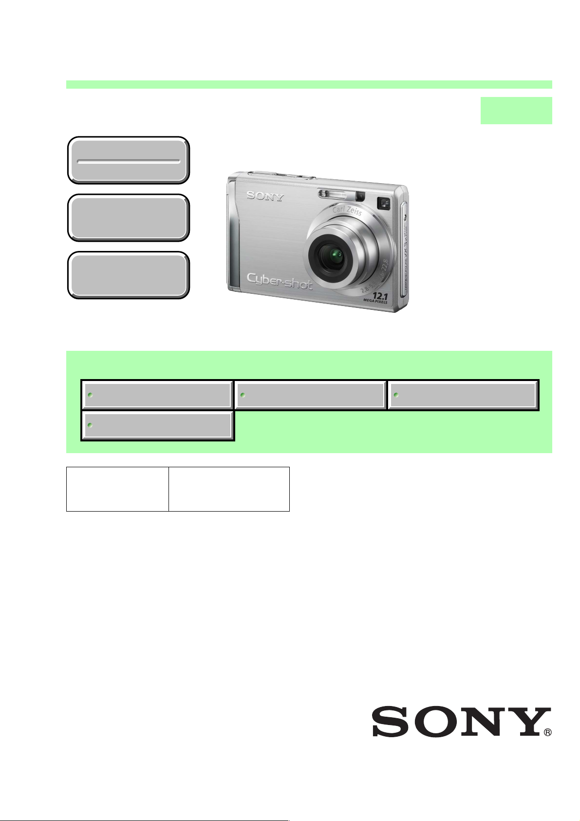
DSC-W200
SERVICE MANUAL
Ver. 1.2 2008.06
Revision History
Revision History
How to use
How to use
Acrobat Reader
Acrobat Reader
Internal memory
Internal memory
ON BOARD
ON BOARD
Link
Link
SERVICE NOTE
PRINTED WIRING BOARDS
LEVEL 3
US Model
Canadian Model
AEP Model
UK Model
E Model
Australian Model
Hong Kong Model
Chinese Model
Korea Model
Argentine Model
Brazilian Model
Japanese Model
Tourist Model
REPAIR PARTS LIST
SCHEMATIC DIAGRAMS
The components identified by
mark 0 or dotted line with
mark 0 are critical for safety.
Replace only with part number specified.
Les composants identifiés par une
marque 0 sont critiques pour la
sécurité.
Ne les remplacer que par une pièce
portant le numéro spécifié.
DIGITAL STILL CAMERA
DSC-W200_L3
Sony EMCS Co.
2008F0800-1
© 2008.06
Published by Kohda TEC9-852-201-11
Page 2

Danger of explosion if battery is incorrectly replaced.
Replace only with the same or equivalent type.
CAUTION
SAFETY-RELATED COMPONENT WARNING!!
COMPONENTS IDENTIFIED BY MARK 0 OR DOTTED LINE WITH
MARK 0 ON THE SCHEMATIC DIAGRAMS AND IN THE PARTS
LIST ARE CRITICAL TO SAFE OPERATION. REPLACE THESE
COMPONENTS WITH SONY PARTS WHOSE PART NUMBERS
APPEAR AS SHOWN IN THIS MANUAL OR IN SUPPLEMENTS
PUBLISHED BY SONY.
SAFETY CHECK-OUT
After correcting the original service problem, perform the following
safety checks before releasing the set to the customer.
1. Check the area of your repair for unsoldered or poorly-soldered
connections. Check the entire board surface for solder splashes
and bridges.
2. Check the interboard wiring to ensure that no wires are
"pinched" or contact high-wattage resistors.
3. Look for unauthorized replacement parts, particularly
transistors, that were installed during a previous repair. Point
them out to the customer and recommend their replacement.
4. Look for parts which, through functioning, show obvious signs
of deterioration. Point them out to the customer and
recommend their replacement.
5. Check the B+ voltage to see it is at the values specified.
6. FLEXIBLE Circuit Board Repairing
• Keep the temperature of the soldering iron around 270°C
during repairing.
• Do not touch the soldering iron on the same conductor of the
circuit board (within 3 times).
• Be careful not to apply force on the conductor when soldering
or unsoldering.
ATTENTION AU COMPOSANT AYANT RAPPORT
À LA SÉCURITÉ!
LES COMPOSANTS IDENTIFÉS PAR UNE MARQUE 0 SUR LES
DIAGRAMMES SCHÉMATIQUES ET LA LISTE DES PIÈCES SONT
CRITIQUES POUR LA SÉCURITÉ DE FONCTIONNEMENT. NE
REMPLACER CES COMPOSANTS QUE PAR DES PIÈSES SONY
DONT LES NUMÉROS SONT DONNÉS DANS CE MANUEL OU
DANS LES SUPPÉMENTS PUBLIÉS PAR SONY.
Unleaded solder
Boards requiring use of unleaded solder are printed with the leadfree mark (LF) indicating the solder contains no lead.
(Caution: Some printed circuit boards may not come printed with
the lead free mark due to their particular size.)
: LEAD FREE MARK
Unleaded solder has the following characteristics.
• Unleaded solder melts at a temperature about 40°C higher than
ordinary solder.
Ordinary soldering irons can be used but the iron tip has to be
applied to the solder joint for a slightly longer time.
Soldering irons using a temperature regulator should be set to
about 350°C.
Caution: The printed pattern (copper foil) may peel away if the
heated tip is applied for too long, so be careful!
• Strong viscosity
Unleaded solder is more viscous (sticky, less prone to flow) than
ordinary solder so use caution not to let solder bridges occur such
as on IC pins, etc.
• Usable with ordinary solder
It is best to use only unleaded solder but unleaded solder may
also be added to ordinary solder.
DSC-W200_L3
— 2 —
Page 3

TABLE OF CONTENTS
Section Title Page
1. SERVICE NOTE
1-4. Method for Copying or Erasing the Data in Internal
Memory (Internal Memory/Music) ································· 1-3
4. PRINTED WIRING BOARDS AND
SCHEMATIC DIAGRAMS
4-2. Schematic Diagrams ························································4-2
4-3. Printed Wiring Boards ··················································· 4-16
4-4. Mounted Parts Location ················································ 4-24
5. REPAIR PARTS LIST
5-2. Electrical Parts List ························································· 5-8
DSC-W200_L3
— 3 —
Page 4

1. SERVICE NOTE
1-4. METHOD FOR COPYING OR ERASING THE DATA IN INTERNAL MEMORY
(INTERNAL MEMORY/MUSIC)
The data can be copied/erased by the operations on the Setup screen. (When erasing the data, execute formatting the internal memory.)
Note 1: When replacing the SY-178 board, erase the data in internal memory of the board before replacement.
Method for Copying the Data in Internal Memory
Copy
Copies all images in the internal memory to a “Memory Stick Duo”.
1 Insert a “Memory Stick Duo” having 64 MB or larger capacity.
2 Select [Copy] with / / / on the control button, then press .
The message “All data in internal memory will be copied” appears.
3 Select [OK] with , then press .
Copying starts.
To cancel the copying
Select [Cancel] in step 3, then press .
•Use a fully charged battery pack. If you attempt to copy image files using a battery pack with little
remaining charge, the battery pack may run out, causing copying to fail or possibly corrupting the data.
•You cannot copy individual images.
•The original images in the internal memory are retained even after copying. To delete the contents of the
internal memory, remove the “Memory Stick Duo” after copying, then execute the [Format] command in
[ Internal Memory Tool ] .
•When you copy the data in the internal memory to the “Memory Stick Duo”, all the data will be copied.
Yo u cannot choose a specific folder on the “Memory Stick Duo” as the destination for the data to be
copied.
•Even if you copy data, a DPOF (Print order) mark is not copied.
Method for Formatting the Internal Memory
This item does not appear when a “Memory Stick Duo” is inserted in the camera.
Format
Formats the internal memory.
•Note that formatting irrevocably erases all data in the internal memory, including even protected images.
1 Select [OK] with v on the control button, then press z.
The message “All data in internal memory will be erased Ready?” appears.
2 Select [OK] with v, then press z.
The format is complete.
To canc el the formatting
Select [Cancel] in step 1 or 2, then press z.
Method for Formatting the Music
Format Music
If you cannot play back a Music file for the Slide Show, the Music file might be corrupted. If
this happens, perform [Format Music].
When [Format Music] is performed, all the Music files are erased. Use the supplied software
“Music Transfer” to activate [Download Music].
1 Select [OK] with v on the control button, then press z.
The message “All data will be erased Ready?” appears.
2 Select [OK] with v, then press z.
All the Music files are erased.
To canc el the formatting
Select [Cancel] in step 1 or 2, then press z.
DSC-W200_L3
1-3
Page 5
Link
Link
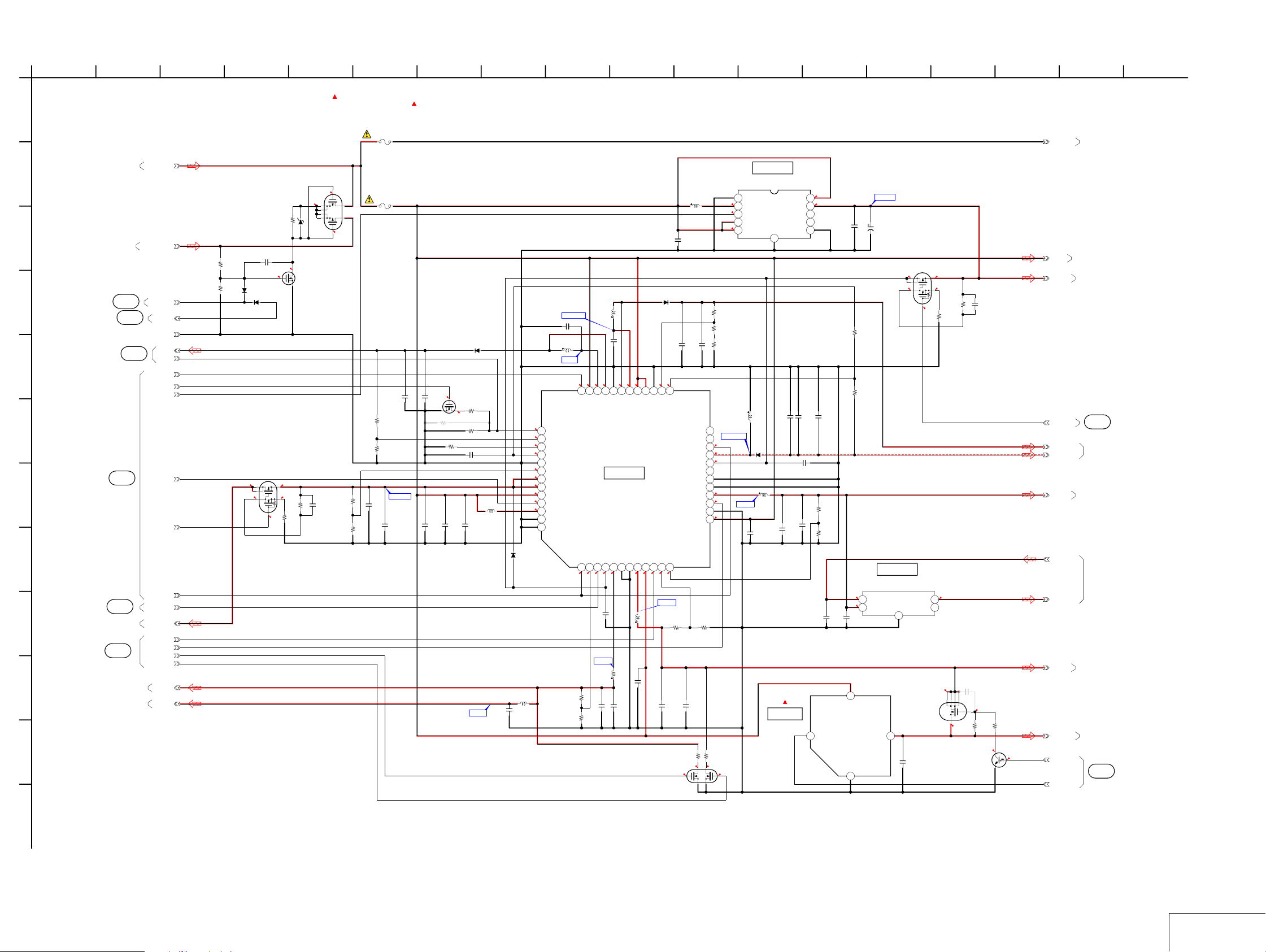
4-2. SCHEMATIC DIAGRAMS
CD-705 FLEXIBLE BOARD (CCD IMAGER)
SY-178 BOARD (1/8) (DC/DC CONVERTER)
SY-178 BOARD (2/8)
(POWER/ENABLE SIG CONTROLLER)
SY-178 BOARD (3/8)
(CAMERA DSP, MODE CONTROL)
SY-178 BOARD (4/8)
(CAMERA DSP, LENS CONTROL, FRONT CONTROL)
COMMON NOTE FOR SCHEMATIC DIAGRAMS
SY-178 BOARD (5/8)
(CCD SIGNAL PROCESS, TIMING GENERATOR)
SY-178 BOARD (6/8) (LENS DRIVER)
SY-178 BOARD (7/8)
(OPTICAL IMAGE STABILIZATION DRIVE)
SY-178 BOARD (8/8) (AUDIO, VIDEO AMP)
DSC-W200_L3
Page 6
4-2. SCHEMATIC DIAGRAMS
4-2. SCHEMATIC DIAGRAMS
4. PRINTED WIRING BOARDS AND SCHEMATIC DIAGRAMS
4-2. SCHEMATIC DIAGRAMS
THIS NOTE IS COMMON FOR SCHEMATIC DIAGRAMS
(In addition to this, the necessary note is printed in each block)
(For schematic diagrams)
• All capacitors are in µF unless otherwise noted. pF : µ
µF. 50 V or less are not indicated except for electrolytics
and tantalums.
• Chip resistors are 1/10 W unless otherwise noted.
kΩ=1000 Ω, MΩ=1000 kΩ.
• Caution when replacing chip parts.
New parts must be attached after removal of chip.
Be careful not to heat the minus side of tantalum
capacitor, Because it is damaged by the heat.
• Some chip part will be indicated as follows.
Example C541 L452
22U 10UH
TA A 2520
Kinds of capacitor
External dimensions (mm)
Case size
• Constants of resistors, capacitors, ICs and etc with XX
indicate that they are not used.
In such cases, the unused circuits may be indicated.
•Parts with ★ differ according to the model/destination.
Refer to the mount table for each function.
• All variable and adjustable resistors have characteristic
curve B, unless otherwise noted.
• Signal name
XEDIT → EDIT PB/XREC → PB/REC
• 2: non flammable resistor
• 5: fusible resistor
• C: panel designation
• A: B+ Line
• B: B– Line
• J : IN/OUT direction of (+,–) B LINE.
• C: adjustment for repair.
• A: not use circuit
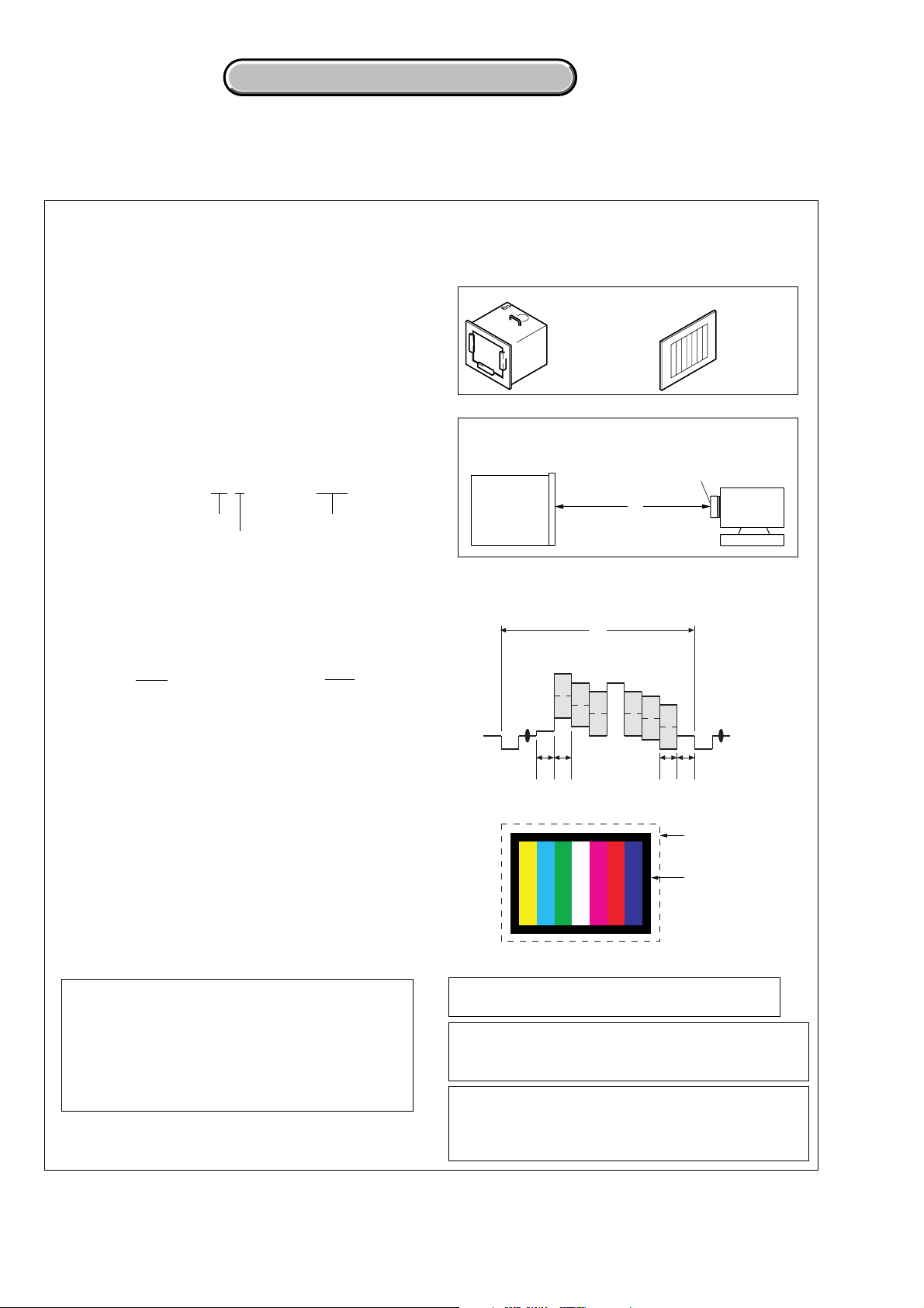
(Measuring conditions voltage and waveform)
•Voltages and waveforms are measured between the
measurement points and ground when camera shoots
color bar chart of pattern box. They are reference values
and reference waveforms.
(VOM of DC 10 MΩ input impedance is used)
•Voltage values change depending upon input
impedance of VOM used.)
1. Connection
Pattern box
Pattern box PTB-450
J-6082-200-A
or
Small pattern box
PTB-1450
J-6082-557-A
L = 24 cm (PTB-450)
L = 11 cm (PTB-1450)
Pattern box
Color bar chart
L
For PTB-450:
J-6020-250-A
For PTB-1450:
J-6082-559-A
Front of the lens
Camera
2. Adjust the distance so that the output waveform of
Fig. a and the Fig. b can be obtain.
H
Yellow
Cyan
White
Magenta
Green
AABBA=B
Fig. a (Video output terminal output waveform)
Fig.b (Picture on monitor TV)
Red
Blue
Electronic beam
scanning frame
CRT picture frame
Precautions for Replacement of Imager
• If the imager has been replaced, carry out all the adjustments
for the camera section.
• As the imager may be damaged by static electricity from
its structure, handle it carefully like for the MOS IC.
In addition, ensure that the receiver is not covered with
dusts nor exposed to strong light.
DSC-W200_L3
When indicating parts by reference number, please
include the board name.
The components identified by mark 0 or dotted line with
mark 0 are critical for safety.
Replace only with part number specified.
Les composants identifiés par une marque 0 sont
critiques pour la sécurité.
Ne les remplacer que par une pièce portant le numéro
spécifie.
4-2
Page 7
1
2
3
4
56
7
8
9
10
11
12
:Voltage measurement of the CSP ICs
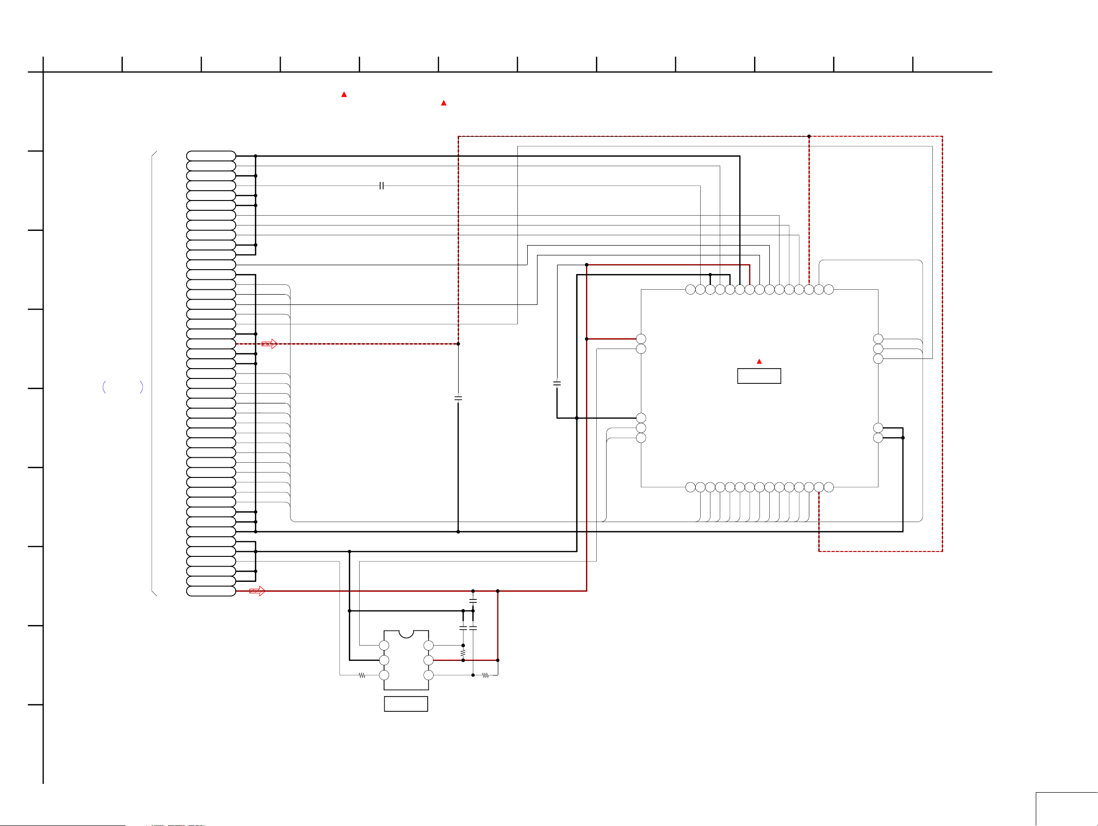
CD-705 FLEXIBLE BOARD
A
CCD IMAGER
and the Transistors with mark,are
not possible.
Voltage of IC002 and IC003 can not
Note:
be measured, because they are mounted
by the side of the lens.
XX MARK:NO MOUNT
LND045
LND044
LND043
B
C
D
SY-178
(5/8)
CN301
PAGE 4-8
of LEVEL3
E
F
G
LND042
LND041
LND040
LND039
LND038
LND037
LND036
LND035
LND034
LND033
LND032
LND031
LND030
LND029
LND028
LND027
LND026
LND025
LND024
LND023
LND022
LND021
LND020
LND019
LND018
LND017
LND016
LND015
LND014
LND013
LND012
LND011
LND010
LND009
LND008
LND007
LND006
LND005
LND004
LND003
LND002
LND001
CAM_VL_CD
CAM_VH_CD
HGND
LH1
HGND
HGND
HGND
H2A
H1B
H1A
HGND
HGND
CONT
VGND
VHLD1
CSUB
VHLD2
SHT
VGND
VGND
VGND
V1A
V1B
V3A
V3B
V3C
V5A
V5B
V5C
V6S1
V6S2
VST2
VST1
TEST
VGND
VGND
AGND
AGND
CCD_OUT
CCD_GND
AGND
45
44
43
RG
42
41
40
39
38
37
36
35
34
33
32
LV
31
30
29
28
27
26
25
24
23
22
21
V2
20
19
18
V4
17
16
15
14
13
12
11
10
9
8
7
6
5
4
3
2
1
LV
VHLD1
VHLD2
V1A
V1B
V2
V3A
V3B
V3C
V4
V5A
V5B
V5C
V6S1
V6S2
VST2
VST1
C007
0.1u
C003
0.22u
C005
0.1u
C008
0.22u
VST1
VST2
LV
26
AGND
LH1
27
28
AGND
29
HGND
30
VDD2
31
CSUB
24RG25
23
NC
VDD
22
VOUT
21
32H333
CONT
34
H2
H1
35VL36
37
LV
NC
VHLD1
VHLD2
SUB
VHLD1
38
VHLD2
39
40
IC003
CCD IMAGER
IC003
ICX612CQZ-13
AGND
20
VST1
19
VST2
18
V5C
12
V5B
V5AV4V3C
V5A13V5B14V5C15V6S1
V3B
V3AV2V1B
V6S2
NC
16
17
V6S2
V6S1
5
V1A
V1A6V1B7V28V3A9V3B10V3C11V4
3
VGND
1
TEST
2
NC4VOG
H
I
08
DSC-W200_L3
IN
1
GND
2
R006
0
OUT
3
IC002
HIGH SPEED BUFFER AMP
CXA3691EN-T9
IC002
ISF
VCC
IDRV
C006
0.01u
6
R007
180k
5
4
C001
0.01u
R003
220k
4-3
CD-705
Page 8
Ver. 1.1 2007.05
• Refer to page 4-2 for mark 0.
1
SY-178 BOARD(1/8)
A
DC/DC CONVERTER
XX MARK:NO MOUNT
NO MARK:REC/PB MODE
B
C
D
(8/8)
(3/8)
(4/8)
2
(8/8)
(3/8)
@001
@002
@003
E
F
@004
G
(2/8)
H
(2/8) (5/8)
@005
I
(3/8) (4/8) (6/8)
(7/8) (8/8)
@006
(2/8)
J
(2/8) (3/8) (4/8) (5/8)
(6/8) (7/8) (8/8)
(4/8) (6/8) (7/8) (8/8)
K
ACV_UNREG
BATT_UNREG
XACV_DET
XACV_IN
REG_GND
BL_H
BL_L
BL_EN1
BL_EN2
EVER_PSB
VSU_EN
DDC5PSW_EN
CAMDD_EN
DDC2P9_EN
MAX_5.0V
DDC1P8_EN
DDC1P2_EN
DISW2P9_EN
DISW1P8_EN
D_3.0V
A_3.0V
16
ST_UNREG
UNREG
TI_5.0V
DDCPV_EN
17
(3/8)
(2/8)
(2/8) (3/8)
(4/8) (5/8)
@007
(2/8)
CAM_12V
CAM_-7.5V
D_1.2V
EVER_3.0V
(5/8)
(3/8) (4/8)
(2/8)
1.2V_INT
D_1.8V
(2/8) (4/8) (7/8)
R038
2200
0
3.0
DDR_1.8V
SW_1P8_EN
(4/8)
@008
LDO_1P8_EN
(2/8)
3.0
5.0
3
0.5
6
R074
4700
3.0
1
2
1.9
15
R075
47k
6
5
2
1
4
1.8
DTC144TMT2L
1.8V SELECT SW
C037
XX
Q012
C063
0.0047u
0
3
R037
220k
P_GND
10
SW
9
PS
8
LBI
7
VBAT
6
L008
4.7uH
D010
MA2SD32008S0
D_1.2V
12
IC002
DC/DC CONVERTER
IC002
SN0510064DRCR
P_PAD
11
C027
4.7u
L009
4.7uH
C028
C024
22u
10u
IC003
1.8V REG
IC003
TK63718AB1G0B
C046
13
3.7
EN
1
5.0
VOUT
2
FB
3
LBO
4
C032
GND
C030
4.7u
C026
1u
R028
22u
2.2u
5
R030
R031
120k
C044
4.7u
24k
R029
100k
3.0
1.2
C034
C061
0.1u
0.1u
B2
Vin
Vcont
A2
GND
A1
TI_5.0V
C033
47u
10V
20k
VOLTAGE DETECTOR
Vin
4
Vsen
3
Vout
1411
5.0
0.5
IC007
IC007
XC6108C10BGR
Vss
5
1.8V SELECT SW
B1
Q014
SSM6E01TU
SW
4
5
1
2
Vout
NC
Q010
SCH1302-TL-E
C035
4.7u
10
1u
C016
3.7
12.0
12.0
3.7
30
31
32
33
PG2
LXLED
LXBST
SWBST
IC001
DC/DC CONVERTER
IC001
MAX8611VETM+TG069
1.8
3.0
L006
4.7uH
C048
10u
D007
MA2SD32008S0
C021
10u
1.0
0
26
27
28GD29
25
FBINV
FBBST
PVBST
SEQCCD
0
1.0
3.7
3.0
D_1.8V
R019
47k
C018
1u
C019
22u
Q007
MCH6604-K-TL-E
1.8V/3.0V DISCHARGE
C020
0
2
22u
C022
10u
CCAUX
ONBST
DRVAUX
ONAUX
R020
100
3.1
L002
4.7uH
FBAUX
LXINV
PVINV
PGSD
LXSD
ONSD
PVSD
C047
22u
3.7
3.0
3.7
R042
680k
R049
51k
R024
2700
24
CAM_-7.5V
23
3.0
22
-7.5
21
5.0
20
19
PG1
18
17
1.2
16
3.7
15
14
3.7
13
R022
56k
R021
100
1.9
6
3
0
5
1
4
R050
C009
C008
4.7u
47u
R014
7
0
XX
C011
MA2SD32008S0
Q006
3LN01SS-TL
SW
R015
0.2
R016
100k
C012
22u
D006
C010
22u
A_3.0V
27
20
0.22u
3
R002
470k
R003
1M
MA2SD32008S0
5.1 5.1
4
MAZS120008SO
C004
1u
2.5
D002
MA2SD32008S0
D003
Q003
SSM6E01TU
5V LOAD SW
4
5
1
2
ACV POWER SELECT SW
D004
R009
470k
0
3
0.60.6
6
R008
470k
R005
3.0
47k
5
Q013
FDW2508PB
3.8
2
3
7
6
Q004
SSM3K03FE(TPL3)
ACV DETECT SW
C060
0.22u
6
:Voltage measurement of the CSP ICs
and the Transistors with mark,are
not possible.
F001
(0.8A/32V)
0
4
1
8
5
0
R012
330k
R013
82k
R010
R011
47k
F002
(2A/32V)
C057
4.7u
1M
MAX_5.0V
C062
10u
C050
47u
L007
2.4uH
C001
22u
8
MA2SD32008S0
L001
22uH
0.2
0.4
1.0
1.3
0.4
5.0
5.0
3.7
3.8
D011
37
38
39
40
41
42
43
44
45
0
46
47
48
49
FBLLED
FBHLED
REXT
REF
GND
FBSU
SU
PVSU
BATT
ONSU
LXSU
PGSU
EP(PAD)
9
L004
4.7uH
CAM_12V
C013
1u
L003
4.7uH
BL_H
3.7
3.7
34
35
36
PVLED
ONLED
SWLED
ONINV2FBM3ONM4PVM5LXM6PGM7PGAFE8LXAFE9PVAFE10ONAFE11FBAFE12FBSD
1
0
0
1.003.1
C015
1u
D_3.0V
L005
4.7uH
R017
68k
C014
10u
R018
33k
18
L
08
DSC-W200_L3
4-4
SY-178 (1/8)
Page 9
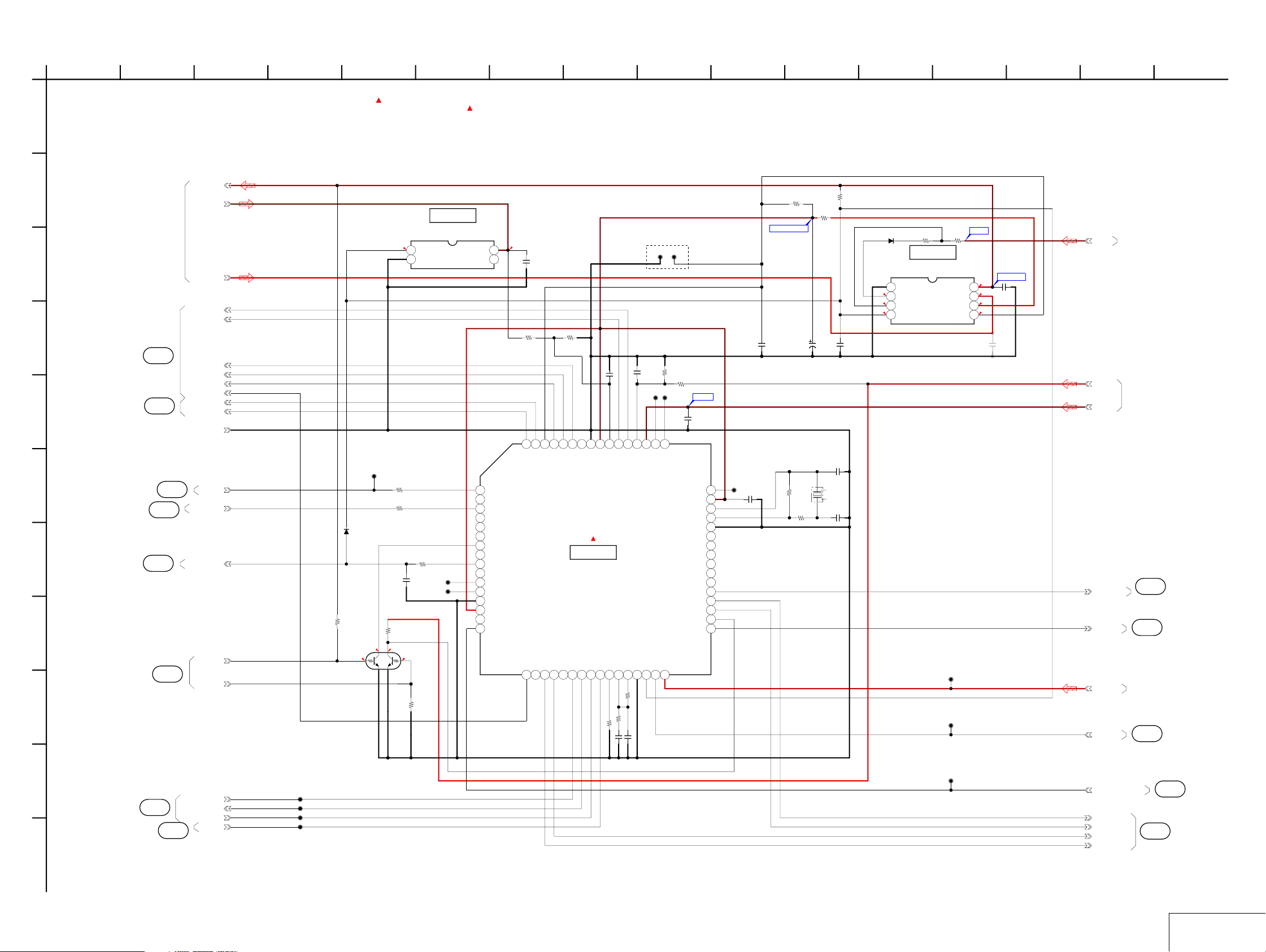
1
2
SY-178 BOARD(2/8)
A
POWER/ENABLE SIG CONTROLLER
XX MARK:NO MOUNT
NO MARK:REC/PB MODE
R:REC MODE
P:PB MODE
3
4
5
:Voltage measurement of the CSP ICs
and the Transistors with mark,are
not possible.
6
7
8
9
10
12
13
1411
15
16
(1/8)
@009
EVER_3.0V
UNREG
TI_5.0V
VSU_EN
EVER_PSB
BL_EN1
BL_EN2
DDC5PSW_EN
CAMDD_EN
SW_1P8_EN
LDO_1P8_EN
REG_GND
XPWR_ON
DIRECT_PB
XDD_SYS_RST
XMS_IN
USB_VBUS
D102
MA2SD32008S0
R119
470k
2
Q101
UP04216008S0
MEMORY STICK /USB DETECT
CL125
03.0
6
3
4
1
3.1
R103
R104
R102
470k
0
0
00
5
VOLTAGE DETECTOR
S-80822CNPF-B8HTFG
Out
1
Vss
2
R125
1k
C119
0.0022u
R105
47k
IC103
IC103
CL106
CL107
VDD
NC
XPOWER_ON0
B8
XPOWER_ON1
A8
XPOWER_ON2
B7
N.C.
A7
N.C.
B6
N.C.
A6
MS_IN
C6
EXT_IN
B5
XSYS_RST
B4
XNAND_RST
C4
TESTPIN
A3
TESTPIN
B3
GND
A4
BACK_UP_VCC
A5
N.C.
A2
XRESET_REQ
A1
R116
R114
47k
BACK_UP_VCC
H7
VSU_EN
CL110
C105
0.047u
CL109
G6
J7
TESTPIN
DDC1P8_AD
DDC2P9_AD
(RESET)
CL112
R109
100k
CL111
H6
TESTPIN
BACK_UP_VCC
R110
100k
TESTPIN
32KHZ_IN
32KHZ_OUT
DDC2P9_EN
DDC1P8_EN
DDC1P2_EN
XUSB_JACK
DDCPV_EN
D_1.8V
C106
0.1u
VSS
N.C.
N.C.
N.C.
N.C.
N.C.
N.C.
C109
0.0047u
X101
32.768kHz
CL113
J6
H4
J4
J5
H5
H1
G2
G1
F1
F2
F3
E9
E8
D9
D8
C9
C107
0.1u
R112
10M
R113
68k
3.7
4
3
C117
0.1u
R121
220k
H2
LDO1P8_EN
R120
220k
F9
F7
D7
J1
XRSTX
BL_EN2
SW1P8_EN
DDC5PSW_EN
POWER/ENABLE SIG CONTROLLER
MB89083LGA-G-133-ERE1
G8
F8
BL_EN1
AF_LED0
IC101
IC101
H9
H8
AVCCG9AVSS
BAAT_SENS
C116 0.1u
J8
J9
EVER_PSB
47k
R126
C110
47u
6.3V
0
0.0022u
C114
D101
MA2SD32008S0
VSS
1
3.1
VCH
2
2.8
VBAT
3
3.0
CS
4
IC102
BACKUP POWER REG
NJU7287ARB1(TE2)
R117
470
IC102
R118
33
VRO
VOUT
XRESET
VL_3V
EVER_3.0V
3.0
8
5.0
7
6
5
C108
C111
0.1u
3.0
3.0
XX
VIN
VL_3V
D_3.0V
(3/8)
(1/8)
D_1.8V
C112
12p
2
4
C113
1
3
12p
DDC2P9_EN
DDCPV_EN
@005
(1/8)
(5/8)
@007
(1/8)
CAMDD_ENB1PANEL_ENC2DISW1P8_ENC1DISW2P9_END3N.C.D1FR_SID2FR_SOE1FR_SCKE2XCS_EXH3MOD0J3VCIJ2CPOG4MOD1A9CSB9XPOWER_OFF
B2
1800
0
0.1u
R107
R106
C103
8200
R108
0.01u
C104
DDC1P2_RESET
C8
CL124
CL122
1.2V_INT
XPWR_OFF
(1/8)
@015
(3/8)
B
C
D
(1/8)
@004
(1/8)
(4/8)
@008
(8/8)
@010
@011
E
F
G
(3/8) (4/8)
(5/8) (7/8)
H
(8/8)
@012
I
J
K
08
DSC-W200_L3
(3/8)
(7/8)
@013
(3/8)
@014
IC211_0_SO
IC211_0_SI
XIC211_0_SCK
XCS_FR
CL101
CL118
CL119
CL120
4-5
CL123
XIC211_RST_REQ
DDC1P8_EN
DDC1P2_EN
DISW2P9_EN
DISW1P8_EN
@016
(3/8)
@006
(1/8)
SY-178 (2/8)
Page 10
1
SY-178 BOARD(3/8)
A
CAMERA DSP MODE CONTROL
XX MARK:NO MOUNT
NO MARK:REC/PB MODE
R:REC MODE
P:PB MODE
2
B
D_3.0V
C
(1/8)
D
E
D_1.2V
F
G
H
I
GEN_SYS_CLK
@017
J
(4/8)
@016
XIC211_RST_REQ
(2/8)
K
L
@011
M
(2/8) (4/8)
(5/8) (7/8)
XDD_SYS_RST
N
REG_GND
D_3.0V
0.1u
ST-168
FLEXIBLE
LND001-LND016
PAGE 4-14
of LEVEL2
2017
3
C211
0.1u
C212
0.1u
C213
0.1u
D_1.2V
C214
0.1u
C215
0.1u
C216
0.1u
C217
0.1u
R225
0
C227
XX
CL208
C201
4
IC211(1/5) IC211(2/5)
CAMERA DSP, LENS CONTROL,
V4
V5
R4
R5
B16
L14
AE24
AF24
AB22
AC23
AC4
Y7
AD1
AD2
AC1
AC2
T10
T11
U10
U11
P10
P11
R10
R11
T12
T13
U12
U13
K16
K17
L16
L17
K15
L15
M16
M17
N16
N17
A20
B20
D21
E21
A22
B22
Y12
AB18
W12
G10
K19
L19
B2
C2
D2
E2
A3
B3
IOVDD
IOVDD
GND
GND
IOVDD
GND
IOVDD
IOVDD
GND
GND
GND
GND
COREVDD
COREVDD
GND
GND
COREVDD
COREVDD
COREVDD
COREVDD
GND
GND
GND
GND
GND
GND
GND
GND
COREVDD
COREVDD
COREVDD
COREVDD
GND
GND
GND
GND
GND
GND
COREVDD
COREVDD
COREVDD
COREVDD
GND
GND
CLK_SYS_IN
XRESET
XRESET_REQ
SIR_RXD
SCLK
SDATA
XRESET
FLMD0
VDD
P14_RXD6
ANIO_P20
P10
FRONT CONTROL
UPD79F0043FC-401-2N1-E2-A
C205
1u
D_3.0V
56
:Voltage measurement of the CSP ICs
and the Transistors with mark,are
not possible.
IC211 (1/5) IC211 (2/ 5)
PRX515101B
D1
E1
A2
P11
VDD
P121_X1
IC201
DSC CONTROL
IC201
REGCD3VSSE3P13_TXD6A4AVSSB4AVREFC4P16
C3
GPS_14
GPS_13
GPS_12
GPS_11
GPS_10
GPS_09
GPS_08
GPS_07
GPS_06
GPS_05
GPS_04
GPS_03
GPS_02
GPS_01
GPS_00
GPE_15
GPE_14
GPE_13
GPE_12
GPE_11
GPE_10
GPE_09
GPE_08
GPE_07
GPE_06
GPE_05
GPE_04
GPE_03
GPE_02
GPE_01
GPE_00
UART0_TXD
UART0_RXD
UART0_CTS
UART0_RTS
UART1_TXD
UART1_RXD
UART1_CTS
UART1_RTS
SID0_SCK
SIO0_SCS
SIO0_TXD
SIO0_RXD
SIO1_SCK
SIO1_TXD
SIO1_RXD
SIO2_SCK
SIO2_TXD
SIO2_RXD
SIO3_SCK
SIO3_TXD
SIO3_RXD
TPU0_OUT
TPU1_OUT
TPU2_OUT
TPU3_OUT
TPU0_INA
TPU0_INB
B1
C1
A1
P120_INTP0
P122_X2_EXCLK
P15
P144_SOA0
P143_SIA0
P142_XSCKA0
P30_INTP1
Y19
W7
Y20
V7
W19
V8
V19
U8
U19
U7
W20
P19
T19
N19
R19
T7
R8
R7
T8
H11
P8
H10
N8
H9
G9
K8
M8
J8
L8
H8
G8
J19
D20
H19
C26
G19
D26
E20
D25
G17
A23
H17
A24
H18
B24
G18
B23
E18
B25
D19
C25
E19
E15
G14
G15
H15
G16
H16
P17
AVREF
TXRX
C228
0.047u
E5
D5
C5
B5
A5
E4
D4
R226
R227
R228 0
R212
10k
CL222
CL219
XCS_IC201
C229
0.047u
0
0
XIC211_1_SCK
IC211_1_SO
IC211_1_SI
C220
0.1u
XCS_IC201
IC211_1_SI
IC211_1_SO
XIC211_1_SCK
MAZS068008SO
7
R213
3300
R214
3300
D201
XHD_EN
XCS_AUDIO
XCS_PANEL
TEST
XAE_LOCK_SW
XSHUT_SW
MS_PWR_ON
VSUB_CONT_PRE
MSHUT_DIR
XLENS_DRIVER_PS
XCS_IC503
XIC211_IC503_RST
XACC_IN
XACV_IN
XFC_RST_LED
XZM_RST_LED
XZM_FG_LED
XPWR_OFF
IC211_1_UO
IC211_1_UI
BOOT_MODE3
XCS_FR
XIC211_0_SCK
IC211_0_SO
IC211_0_SI
XIC211_2_SCK
IC211_2_SO
XCS_FE
XCS_TG
XIC211_3_SCK
IC211_3_SO
IC211_3_SI
8
@018
@019
@020
@022
@015
(1/8) (8/8)
(4/8)
@021
@023
@024
@025
@026
@002
@027
@028
@014
@013
@029
@030
(2/8)
(8/8)
(4/8)
(8/8)
(8/8)
(8/8)
(1/8)
(6/8)
(8/8)
(2/8)
(2/8)
(7/8)
(4/8)
(8/8)
(5/8)
BATT_UNREG
(5/8)
(6/8)
(7/8)
9
R723
820
CL-271HR-C-TS
(MS ACCESS)
(5/8)
10
D706
L211
CAM_3.5V
BATT_UNREG
BATT_SIG
REG_GND
CAM_3.5V
R224
XX
LND704
LND705
LND706
10uH
BT-037
FLEXIBLE
LND001-LND003
PAGE 4-15
of LEVEL2
12 19
B12
L13
D_3.0V
C225
0.1u
A12
K13
C226
XX
E8
D8
R215
R216
100
620
W1
V1
AA4
AB2
AA2
C223
AB4
0.1u
AB1
C222
22u
6.3V
Y2
W4
Y4
AB5
W2
W5
C224
0.1u
E22
E23
D23
D22
F22
H13
AB15
AB16
A21
B21
D15
H14
13
CAMERA DSP, LENS CONTROL,
FRONT CONTROL
PRX515101B
MS_IOVDD
GND
MSX_IOVDD
GND
SD_IOVDD
GND
RREF
NC
GNDS
AVDD1
AGND1
AVDD2
AGND2
AVDD3
AGND3
ADVDD
AGND
DVDD
DVSS
BOOT_MODE_4
BOOT_MODE_3
BOOT_MODE_2
BOOT_MODE_1
BOOT_MODE_0
TEST
EXT_CK_PLL2
EXT_CK_PLL3
EXT_SEL_1
EXT_SEL0
PLL_BYPASS
PCV
1411
Note : IC211 is not supplied,
but this is included in SY-178 complete board.
B10
MS_BS
A9
MS_B_3
B11
MS_B_2
A10
MS_B_1
B9
MS_B_0
A11
MS_CLK
MSX_BS
MSX_B_3
MSX_B_2
MSX_B_1
MSX_B_0
MSX_CLK
SD_CLKOUT
SD_CMD
SD_DAT_3
SD_DAT_2
SD_DAT_1
SD_DAT_0
SD_WP
SD_XCD
USB_ID
USB_VBUS_EN
SA_TDO
SA_TD1
NTRST
JTAG_SEL1
JTAG_SEL0
VBUS
RTCK
DM
TDI
TCK
TMS
TDO
DP
A14
A13
B14
B13
A15
B15
D11
E10
D10
E11
D9
E9
E12
D12
AA5
Y5
V2
Y1
AA1
U4
U5
D13
G11
E13
G12
G13
D14
E14
H12
@033
(4/8)
@034
(4/8)
(1/8)
(1/8)
FB230
FB231
FB232
FB233
FB234
CL220
CL221
CL211
CL212
CL213
CL214
CL215
CL216
CL217
CL218
(2/8)
XAE_LOCK_LED
VL_3V
ST_UNREG
TI_5.0V
STRB_ON1
XSTRB_LED
MAX_5.0V
R217
R218
R219
R220
R221
R222
15
100
150
150
150
150
150
Q711
SSM3J09FU(TE85L)
AF LOCK LED SW
0
3.1
3.1
AF LOCK LED SW
R769
10k
16
MSX_BS
MSX_D3
MSX_D2
MSX_D1
MSX_D0
MSX_CLK
USB_DP
USB_DM
Q713
DTC114EMT2L
R733
1800
R735
7500
@031
(8/8)
@032
(8/8)
R701
D707
MA2SD32008S0
R767
68
1.6
R730
C726
100k
100p
5.0 5.0
0
2
220
R731
820
Q712
SSM3J09FU(TE85L)
STRBE LED SW
000
3.1
3.1
Q714
R770
DTC114EMT2L
10k
STRBE LED SW
6
3
0
5
R734
Q704
1
4
EMX1T2R
AF LED DRIVE
0
R732
R768
68
5.0
2SA2029T2LQ/R
AF LED DRIVE
15
15
1.7
0.15.0
Q710
18
CN714 16P
REG_GND
16
VL_3V
15
ST_UNREG
14
ST_UNREG
13
TI_5.0V
12
STRB_ON
11
STB_CHG_CNT
10
STRB_CHG
9
XSTRB_FULL
8
D_3.0V
7
XAE_LOCK_LED
6
XSTRB_LED
5
AF_5.0V
4
XAF_LED
3
REG_GND
2
REG_GND
1
O
08
DSC-W200_L3
4-6
SY-178 (3/8)
Page 11

1
SY-178 BOARD(4/8)
A
CAMERA DSP, LENS CONTROL, FRONT CONTROL
XX MARK:NO MOUNT
NO MARK:REC/PB MODE
R:REC MODE
P:PB MODE
2
B
DDR_1.8V
C
(1/8)
D_1.8V
FB281
C287
22u
FB283
D
E
F
C282
0.1u
G
H
I
J
K
L
M
N
O
REG_GND
3
CAMERA DSP, LENS CONTROL,
C1
VDDQ(POP-DDR)
C2
C283
0.1u
C284
0.1u
VDDQ(POP-DDR)
H1
VDD(POP-DDR)
H2
VDD(POP-DDR)
A2
GND(POP-GND)
B1
GND(POP-GND)
G1
GND(POP-GND)
G2
GND(POP-GND)
E1
VDDQ_O(POP-FLASH)
E2
VDDQ_O(POP-FLASH)
F1
VDD_O(POP-FLASH)
F2
VDD_O(POP-FLASH)
D2
GND(POP-GND)
F4
GND(POP-GND)
F5
GND(POP-GND)
G4
GND(POP-GND)
G5
GND(POP-GND)
A7
EMC_VDD
B7
EMC_VDD
D7
C281
EMC_VDD
0.1u
A8
GND
B8
GND
K10
EMC_VDD
K11
EMC_VDD
L10
EMC_VDD
L11
EMC_VDD
M10
GND
M11
GND
N10
GND
N11
GND
K12
GND
L12
GND
L5
EMC_ADDR_24
L1
EMC_ADDR_23
L4
EMC_ADDR_22
M1
EMC_ADDR_15
L7
EMC_ADDR_14
N1
EMC_ADDR_13
K7
EMC_ADDR_12
N5
EMC_ADDR_11
L2
EMC_ADDR_10
M5
EMC_ADDR_09
N2
EMC_ADDR_08
N7
EMC_ADDR_07
N4
EMC_ADDR_06
P7
EMC_ADDR_05
M4
EMC_ADDR_04
M7
EMC_ADDR_03
M2
EMC_ADDR_02
P5
EMC_ADDR_01
P4
EMC_ADDR_00
A3
EMC_DATA_15
B3
EMC_DATA_14
A4
EMC_DATA_13
B4
EMC_DATA_12
B5
EMC_DATA_11
A5
EMC_DATA_10
B6
EMC_DATA_09
A6
EMC_DATA_08
E4
EMC_DATA_07
B2
EMC_DATA_06
E5
EMC_DATA_05
D4
EMC_DATA_04
E6
EMC_DATA_03
D5
EMC_DATA_02
E7
EMC_DATA_01
D6
EMC_DATA_00
H4
EMC_XOE
K4
EMC_XWE
H7
EMC_XCS_2
G7
EMC_XCS_1
J4
EMC_XCS_0
H5
EMC_XRAS
D1
EMC_CLK_IN_SDRAM
J1
EMC_CLK_OUT_FLASH
K1
EMC_CLK_IN_FLASH
J5
EMC_RDY0
J7
EMC_RDY1
J2
EMC_XRST
K5
EMC_DRQIN
K2
EXTINT18
M19
STABLE_RUN
4
FRONT CONTROL
IC211 (5/5)
PRX515101B
56
T16
DDR_VDD
DDR_VDD
DDR_VDD
DDR_VDD
DDR_VDD
DDR_VDD
DDR_VDD
DDR_VDD
DDR_VDD
DDR_VDD
DDR_ADDR_14
DDR_ADDR_13
DDR_ADDR_12
DDR_ADDR_11
DDR_ADDR_10
DDR_ADDR_09
DDR_ADDR_08
DDR_ADDR_07
DDR_ADDR_06
DDR_ADDR_05
DDR_ADDR_04
DDR_ADDR_03
DDR_ADDR_02
DDR_ADDR_01
DDR_ADDR_00
DDR_BA_1
DDR_BA_0
DDR_XWE
DDR_XRAS
DDR_XCAS
DDR_XCS_1
DDR_CKE2
DDR_XCS_0
DDR_CKE1
DDR_CLK
DDR_DCLKN
DDR_DQS_3
DDR_DQM_3
DDR_DATA_31
DDR_DATA_30
DDR_DATA_29
DDR_DATA_28
DDR_DATA_27
DDR_DATA_26
DDR_DATA_25
DDR_DATA_24
DDR_DQS_2
DDR_DQM_2
DDR_DATA_23
DDR_DATA_22
DDR_DATA_21
DDR_DATA_20
DDR_DATA_19
DDR_DATA_18
DDR_DATA_17
DDR_DATA_16
DDR_DQS_1
DDR_DQM_1
DDR_DATA_15
DDR_DATA_14
DDR_DATA_13
DDR_DATA_12
DDR_DATA_11
DDR_DATA_10
DDR_DATA_09
DDR_DATA_08
DDR_DQS_0
DDR_DQM_0
DDR_DATA_07
DDR_DATA_06
DDR_DATA_05
DDR_DATA_04
DDR_DATA_03
DDR_DATA_02
DDR_DATA_01
DDR_DATA_00
GND
GND
GND
GND
GND
GND
GND
GND
GND
GND
GND
GND
FB282
T17
U16
C285
U17
0.1u
T14
T15
U14
U15
P16
P17
R16
R17
Y22
W23
W25
W26
Y25
Y26
AA22
C286
Y23
0.1u
AA25
AA26
K22
L22
L26
K23
L25
L20
J23
M22
L23
M20
M23
N22
N26
N20
N25
K25
K26
P20
P22
N23
P25
P26
R20
R22
M26
M25
G26
G25
E26
F26
E25
G22
F25
G20
F23
H20
J26
J25
H22
J20
G23
J22
H26
K20
H25
H23
R26
T26
T25
R23
R25
T20
U25
P23
U26
T22
V26
V25
U23
U22
T23
U20
W22
V22
V23
V20
7
:Voltage measurement of the CSP ICs
and the Transistors with mark,are
not possible.
D_3.0V
(1/8)
A_3.0V
STRB_ON1
@033
(3/8)
VSUB_CONT_POST
@035
(5/8)
MSHUT_EN
FC_DIR_A
FC_DIR_B
FC_EN_A
ZM_DIR_A
@036
(6/8)
ZM_EN_A
ZM_BRK_B
IRIS_M_EN
IRIS_M_IN
IRIS_S_IN
IRIS_S_EN
ZM_SENS_1ST
R205
0
C202
4.7u
6.3V
R211
R204 0
0
C207
XX
C260
0.1u
R299
10k
R279
47k
C259
0.1u
C256
0.1u
IC211_CVOUT
C261
0.1u
VOUT_1
VOUT_2
18
R275
R272
10k
10k
MODE_DIAL1
MODE_DIAL2
KEY_AD_1
KEY_AD_2
LENS_TEMP
TZ_HALL_TEMP
IC211_AUIN
@043
IC211_AUOUT
IC211_CVOUT
@042
(6/8)
(2/8) (3/8)
(5/8) (7/8)
(8/8)
2017
Note : IC211 is not supplied,
(2/8)
@010
(1/8)
@011
@029
(3/8)
(8/8)
@020
(3/8)
(1/8)
2112 19
but this is included in SY-178 complete board.
DIRECT_PB
BL_L
BL_H
@003
XDD_SYS_RST
IC211_2_SO
XIC211_2_SCK
XCS_PANEL
TEST
TI_5.0V
MAX_5.0V
LCD_VD
LCD_HD
LCD_D7
LCD_D6
LCD_D5
LCD_D4
LCD_D3
LCD_D2
LCD_D1
LCD_CK
R773
XX
R771
22
C731
1u
XX
IC701
XX
R752
XX
R1114Q311D-TR-FA
23 24 25 26
CN708
REG_GND
8
KEY_AD1
7
KEY_AD2
6
XDIRECT_PB
5
BL_L
4
BL_H
3
MODE_DIAL2
2
MODE_DIAL1
1
CN713 39P
VCOMI
39
C709
4.7u
VCOMO
38
XRST
37
0
R739
R740
R741
XCS
36
0
SI
35
0
XSCK
34
VSSA
33
VDD1A
32
VDD1D
31
NC
30
NC
29
NC
28
NC
27
NC
26
VDD2IN
25
VSSD
24
0.47u
C710
VSS2C1
23
VSS2C2
22
VSS2OUT
21
VSS2IN
20
NC
19
NC
18
0.1u
C711
VSS3C1
17
VSS3C2
16
VSS3OUT
15
VSS3IN
14
Vsync
13
Hsync
12
MCK
11
D7
10
D6
9
D5
8
D4
7
D3
6
D2
5
D1
4
TESTOUT
3
R763
VSSD
2
100k
Dummy1
1
45
C719
XX
IC702
LCD 3.1V REG
IC702
5.0
4
VIN
CE
1
3.0
KEY_AD_1
KEY_AD_2
MODE_DIAL2
MODE_DIAL1
R764
C730
1k
0.1u
L702
10uH
C708
10u
C706
10u
C713
C720
2.2u
XX
CL704
CL703
CL702
CL701
R762
150k
123
3.1
3
R775
C732
100K
0.47u
VOUT
VSS
2
8P
SW-501
CN001
PAGE 4-13
of LEVEL2
LCD901
2.5inch
COLOR
LCD
MONITOR
XX
10u
3.5
15
CAMERA DSP, LENS CONTROL,
AC15
AVCC_PLL1
AE16
AVSS_PLL1
AE15
AVCC_PLL2
AC16
AVSS_PLL2
AF15
AVCC_PLL3
AF16
AVSS_PLL3
AE5
AVCC_CTRLADC
AC6
AVSS_CTRLADC
AB14
GND
AC14
GND
AE14
GND
AF14
GND
P1
GND
P2
GND
U1
GND
U2
GND
AF9
AVCC_AUADC
AE9
AVSS_AUADC
AF11
AVCC_AUDAC
AC10
AVSS_AUDAC
AF13
AVCC_VIDEODAC
AC11
AVSS_VIDEODAC
3.1
4
3
1
256
0.1
R260
180
R258 2200
R261
150
R259
R262
150
FRONT CONTROL
PRX515101B
R257
1k
LCD_DATA_7
LCD_DATA_6
LCD_DATA_5
LCD_DATA_4
LCD_DATA_3
LCD_DATA_2
LCD_DATA_1
LCD_DATA_0
LCD_CLK_OUT
LCD_XHD_OUT
LCD_XVD_OUT
SYSV_OUT
CAMV_OUT
CLK_IC503
CLKGEN_DIV2
CCDIN_A_13
CCDIN_A_12
CCDIN_A_11
CCDIN_A_10
CCDIN_A_09
CCDIN_A_08
CCDIN_A_07
CCDIN_A_06
CCDIN_A_05
CCDIN_A_04
CCDIN_A_03
CCDIN_A_02
CCDIN_A_01
CCDIN_A_00
TGCLK_IN
CCD_SYNC_SEL
CK_AD_IN
CLAMP_OPB
TG_OUT
ICLK
GEAR_ON
VDDO
X201
38MHz
C206
0.1u
SENS0
SENS2
CCD_FD
CCD_HD
C208
XX
10
0
CL241
R250
0
C266
0.001u
0.001u
GEN_SYS_CLK
R280
C263
LCD_D7
LCD_D6
LCD_D5
LCD_D4
LCD_D3
LCD_D2
LCD_D1
LCD_CK
LCD_HD
LCD_VD
XSTRB_LED
XAE_LOCK_LED
XPWR_LED
0
R294XXR295
C264
0.001u
CLK_IC503
CA_AD13
CA_AD12
CA_AD11
CA_AD10
CA_AD09
CA_AD08
CA_AD07
CA_AD06
CA_AD05
CA_AD04
CA_AD03
CA_AD02
CA_AD01
CA_AD00
GEN_TG_CLK
CA_HD
CA_FD
@017
(3/8)
@034
(8/8)
@037
FC_SENS
XX
ZM_DC_FG_1A
ZM_DC_FG_1B
@039
(7/8)
@040
(5/8)
@041
(5/8)
(7/8)
A17
D16
A18
E16
A19
E17
B19
R290
D17
B18
D18
B17
W9
LED0
Y9
LED1
W8
LED2
Y10
W10
R289
XX
R281
XX
Y11
FG1A
W11
FGAB
W14
Y14
W13
Y13
AE18
AF19
AE19
AF20
AE20
AF21
AE21
AC18
AC19
AB19
AC20
AB20
AC21
AB21
R241
0
AF18
AF23
AF22
AE23
AC22
AE22
R206
39
1.6
1
1.5
2
3.1
3
3.1
4
8
C267
0.1u
C242
0.1u
C262
0.1u
C243
0.1u
C241
0.1u
C265
0.001u
C204
0.1u
C203
0.1u
R209
0
9
IC211(3/5) IC211(4/5)IC211(5/5)
CAMERA DSP, LENS CONTROL,
FRONT CONTROL
IC211 (3/5 ) IC211 (4/5)
PRX515101B
A1
NC
AE1
NC
AF1
NC
AF2
NC
A25
DDR_IOVDD
A26
NC
B26
DDR_IOVDD
AF26
NC
A16
LCD_IOVDD
K14
GND
Y8
AVCC_LED
AB10
AVSS_LED
AB12
AVCC_PI
AB11
AVSS_PI
AE17
CCD1_IOVDD
AC17
CCD2_IOVDD
AB17
CCD3_IOVDD
AF17
GND
AE25
MSHUT_EN
Y16
STRB_ON1
AE26
STRB_ON2
Y15
STRB_ON3
AF25
VSUB_CONT
W18
DIR0A
AB26
DIR0B
W17
BRK0A
AB25
BRK0B
AB23
DIR1A
AC26
DIR1B
AA23
BRK1A
AC25
BRK1B
W16
DIR2A
Y18
DIR2B
AD25
BRK2A
Y17
BRK2B
AD26
SENS1A
W15
SENS1B
IC202
LOW POWER CLOCK GEN
IC202
ICS620AN-29LFT
1.9
VDD
8
GND
7
3.1
VDDO
6
1.5
SYS_OUT
5
GND
9
R203
R210
0
33
(3/8)
@038
(6/8)
(8/8)
@018
(3/8)
(1/8)
AU_AVCC
D_1.2V
XHD_EN
13
L241
10uH
R253
R291
R254
R292
FB255
R293
XX
R256
0
IC211_CVOUT
VOUT_1
VOUT_2
1411
C246
22u
22
XX
C247
22u
22
XX
R300
C248
22u
C249
22u
C251
0.1u
C245
L242
10uH
C250
10u
Q241
SCH1302-TL-E
SW
2200
ADC0_IN1
ADC0_IN2
ADC0_IN3
ADC0_IN4
ADC0_IN5
ADC0_IN6
ADC0_IN7
ADC0_IN8
ADC1_IN1
ADC1_IN2
ADC1_IN3
ADC1_IN4
ADC1_IN5
ADC1_IN6
ADC1_IN7
ADC1_IN8
AUCK_IN
ADCK_OUT
AUCK_OUT
SCLK_OUT
Q242
2SA2029T2LQ/R
Y MUTE
Q243
2SA2029T2LQ/R
PB MUTE
Q244
2SA2029T2LQ/R
PR MUTE
VREF0
VOUT0
VREF1
VOUT1
VOUT2
16
R298
C252
0.1u
C253
0.1u
IC211_YOUT
IC211_PBOUT
IC211_PROUT
10k
R276
47k
C254
0.1u
C257
0.1u
R270
1k
R269
3600
R271
1k
R273
100k
R267
56k
R274
100k
R268
56k
@044
(8/8)
R296 0
AB7
R297 0
AE6
R264 0
AC8
R265 0
AF6
AC7
AE7
AB8
AF7
AE3
AE4
AE2
AF3
AC5
AF5
AB6
AF4
R2
T5
SIA
R1
SOA
T4
T1
T2
AF8
AIN
AC9
VRH
AB9
VRL
AE8
AOUT
AE10
VRP
AF10
VRN
R263
2200
AE11
VRD0
AE12
AB13
R266
2200
AE13
VRD1
AC13
AF12
AC12
08
DSC-W200_L3
4-7
SY-178 (4/8)
Page 12

1
SY-178 BOARD(5/8)
A
CCD SIGNAL PROCESS, TIMING GENERATOR
XX MARK:NO MOUNT
NO MARK:REC/PB MODE
R:REC MODE
P:PB MODE
2
3
4
56
:Voltage measurement of the CSP ICs
and the Transistors with mark,are
not possible.
7
8
9
10
13
1411
15
16
18
2017
2112 19
22
23
B
D301
C302
0.1u
0
Q302
DTC144EMT2L
SWITCH
Q301
SWITCH
CL325
R305
100k
3.1
1SS387CT(TL3SONY)
C303
1u
CL327
R340
47k
C327
C326
R347
130k
0
6
3
2
4
1
CL308
CL313
C328
C344
C343
C345
R301
910k
0
XX
0.001u
CL328
CL315
CL316
CD_V4
CD_V2
CD_V3C
CD_V3A
CD_V5B
CD_V1A
R344
0
H14VRJ14HRM8
D8
D12
D9
D10
D11
K4
B9
E12
F12
K15
L15
F4
H4V1C2V2A4
SSI
SCK
SEN1
SOUT
SEN2(VDr)
TDO
N14
TMS
M14
TDI
L14
TCK
K14
TEST3
M5
TRST
L4
SOUTV
J4
RSV3
M6
RSV2
M7
RSV1
P8
RSV0
P9
R341
STATE
M9
0
IREFVDR
G15
HLSW
E4
U0
D4
LASTH
R7
RG
R8
H2B
P15
H2A
P14
H1B
R13
H1A
R14
TP_SHD
M11
TP_SHP
M12
TP_ADCLK
M10
TP_CLPOB
K12
TP_CLPDM
L12
BYPD
E15
CCDIN
C15
CCDGND
C14
0.1u
L
A14
0.1u
REFP
A13
0.1u
CM
A12
0.1u
REFN
A11
DLLVSSP6HVSSLHP7HVSSRG
HVSS1R9HVSS2
HVSS3
HVSS4
P10
P11
4.5
5
CL326
B12
F14
R10
C304
4.7u
RESET
AVSS2
D15
GPO0B8GPO1B7GPO2
RST(VDr)
AVSS1
AVSS1
D14
GNDS
AVSS1
B11
B15
TRIG
MCKV
MCKTA
TGSTBY
IC301
CCD SIGNAL PROCESS,
TIMING GENERATOR
IC301
CXD4806GA-T4
AVSV1
GNDS
J12
G14
C1V4A3
V3AB4V3B
DVSS1
V5AB3V5B
DLLVDDP4DRVSSP5DRVSSM4DRVSS
DVSS1
F15
J15
0.1u
C342
SUB
DVSS2J2DVSS3B5PVSS
M15
A10
CD_V1B
CD_V5C
CD_V6S1
G1V6H2V7F2V8G4V9G2
AVDD1
AVDD2
B14
E14B13
0.1u
C340
CD_V6S2
0.1u
C339
CD_V3B
HVDDLHR5HVDDRGR6AVDD1
CD_V5A
CD_VST1
CD_VST2
V10F1V11D2V12E2V13D1V14
HVDD2
HVDD3
HVDD4
R12
R11
P12
P13
C338 0.1u
CD_VHLD1
CD_VHLD2
HVDD1
G12
AVDV2
DRVDD
DVDD1
DVDD1
DVDD2
DVDD3
AVDV1
XV14
XV15
XV12
XV13
PVDD
CD_LV
V15
E1
VH
A2
VL
B2
VM
B1
XP8
C329
0.1u
CL329
D_3.0V
C330
0.1u
CA_AD00
CA_AD01
CA_AD02
CA_AD03
CA_AD04
CA_AD05
CA_AD06
CA_AD07
CA_AD08
CA_AD09
CA_AD10
CA_AD11
CA_AD12
CA_AD13
C331 0.1u
C332
C334
C335 0.1u
D_3.0V
R326
0
C348
XX
R325
0
C363
XX
L301
L302
0.1u
0.1u
C309
47u
6.3V
R350
100
7.5
SSM3J15FV(TL3SONYZ)
-7.5V DISCHARGE
0
R351
100k
10uH
10uH
R324
0
C307
C346
C320
47u
XX
6.3V
Q303
C349
1u
C319
22u
0.01u
FB302
FB303
L303
10uH
C305
R310
22u
100k
10V
C315
10u
C362
22u
4V
1.2
3
2
3.1
1
C306
4.7u
R353
220k
3.1
2
3.0
CE
1
VSS
2
3.1
CE
1
VSS
2
IC303
2.8V REG
IC303
TK70628HCL-G
CNp Vout
GND
Vcnt
R328
0
R352
750
3.5
0
6
3
4
1
MCH6604-K-TL-E
3.5V DISCHARGE
5.0
Vin
4
3.5
Vout
3
3.1
Vin
4
2.3
Vout
3
4
GND
5
Vin
6
IC304
NJM2831F13(TE1)
13.7
1
2
C322
1u
34
0
5
Q304
A7
XP9
A9
A6
XV6
D7
XV7
B6
A8
D5
D6
B0
J1
B1
L2
B2
M1
B3
N2
B4
P2
B5
R3
B6
K2
B7
K1
B8
L1
B9
M2
B10
P3
B11
R2
B12
P1
B13
N1
R4
H15
N15
B10
H1
A5
H12
R302
C308
C
CN301
45P
HGND
45
LH1
44
HGND
43
RG
42
HGND
D
E
F
CD-705
FLEXIBLE
LND001-LND045
PAGE 4-3
of LEVEL3
G
H
I
HGND
HGND
HGND
CONT
VGND
VHLD1
CSUB
VHLD2
VGND
CAM_VL_CD
VGND
VGND
VGND
VGND
AGND
AGND
CCD_OUT
CCD_GND
AGND
CAM_VH1
41
40
H2A
39
H1B
38
H1A
37
36
35
34
33
LV
SHT
V1A
V1B
V2
V3A
V3B
V3C
V4
V5A
V5B
V5C
V6S1
V6S2
VST2
VST1
TEST
CD_LV
32
CD_VHLD1
31
30
CD_VHLD2
29
28
27
26
25
24
CD_V1A
23
22
21
20
19
18
17
16
15
14
13
12
11
10
9
8
7
6
5
4
3
2
1
CD_V1B
CD_V2
CD_V3A
CD_V3B
CD_V3C
CD_V4
CD_V5A
CD_V5B
CD_V5C
CD_V6S1
CD_V6S2
CD_VST2
CD_VST1
C350
C351 XX
C352 XX
C353 XX
C354 XX
C355 XX
C356 XX
C357 XX
C358 XX
C359 XX
C360 XX
C361 XX
XX
0.0022u
0
R304
9.0
220k
R303
1M
R339
R332
36
R330
R334
R333
R331
R307
R306
0
56
0
R338
R337
0
3.9
R336
0
3.9
R335
3.9
0
C324
0.1u
0
C325
0
0.1u
R308
0
J
K
R321
0
L
C310
0.1u
C301
4.7u
10V
M
RN1904AFS(TLR3SONY)
FB301
N
C314
1u
C316
1u
2.8
3.1
12V REG
IC304
Vcnt
GND
Np
5
Vin
Vout
CL330
CL332
CL333
CL334
CL335
CL336
CL331
CA_AD13
CA_AD12
CA_AD11
CA_AD10
CA_AD09
CA_AD08
CA_AD07
CA_AD06
CA_AD05
CA_AD04
CA_AD03
CA_AD02
CA_AD01
CA_AD00
TI_5V
IC305
3.5V REG
IC305
R1114Q351D-TR-FA
D_3.0V
IC302
2.3V REG
IC302
R1114Q231D-TR-FA
C318
1u
13.7
13.1
CAM_12V
C321
1u
CA_FD
XDD_SYS_RST
XCS_FE
XIC211_3_SCK
IC211_3_SO
IC211_3_SI
XCS_TG
CA_HD
GEN_TG_CLK
CA_AD13
CA_AD12
CA_AD11
CA_AD10
CA_AD09
CA_AD08
CA_AD07
CA_AD06
CA_AD05
CA_AD04
CA_AD03
CA_AD02
CA_AD01
CA_AD00
CAM_3.5V
DDC2P9_EN
TI_5.0V
D_3.0V
REG_GND
CAM_-7.5V
CAM_12V
VSUB_CONT_POST
VSUB_CONT_PRE
@041
@011
@040
(3/8)
@005
(1/8)
(1/8)
(4/8)
(7/8)
@030
@035
@023
(2/8) (3/8)
(4/8) (7/8)
(3/8)
(4/8)
(1/8)
(2/8)
(4/8)
(3/8)
08
DSC-W200_L3
4-8
SY-178 (5/8)
Page 13

1
2
SY-178 BOARD(6/8)
A
LENS DRIVER
XX MARK:NO MOUNT
NO MARK:REC/PB MODE
R:REC MODE
P:PB MODE
3
4
5
:Voltage measurement of the CSP ICs
and the Transistors with mark,are
not possible.
6
7
8
9
10
12
13
1411
15
16
17
18
B
CN402
51P
51
4(-)
50
4(+)
ND(+)
49
ND(-)
C
D
YAW_HALL_BIAS+
YAW_HALL_BIAS-
PITCH_HALL_BIAS+
PITCH_HALL_BIAS-
E
LENS
BLOCK
F
G
H
GND(LENS THERM)
GND(Z_PI_SENS)
Z_PI_SENS_Vcc
Z_PI_SENS_OUT
F_PI_SENS_Vcc
F_PI_SENS_OUT
Z_BOX2_PI_SENS_Vcc
Z_BOX2_PI_SENS_Col
Z_BOX1_PI_SENS_Vcc
Z_BOX1_PI_SENS_Col
Z_DC_MOTOR(-)
Z_DC_MOTOR(-)
Z_DC_MOTOR(-)
Z_DC_MOTOR(+)
Z_DC_MOTOR(+)
Z_DC_MOTOR(+)
F_MOTOR_B(-)
F_MOTOR_A(-)
SHUTTER(-)
SHUTTER(-)
SHUTTER(+)
SHUTTER(+)
PITCH+
PITCH+
GND
YAW_HALL_-
YAW_HALL_+
GND
YAW-
YAW-
THERM
PITCH_HALL-
PITCH_HALL+
YAW+
YAW+
PITCH-
PITCH-
LENS THERM
XFC_RST_LED
XZM_FG_LED
XZM_FG_LED
F_MOTOR_A
F_MOTOR_B
48
47
46
45
44
43
42
41
40
39
38
37
36
35
34
33
32
31
30
29
28
27
26
25
24
23
22
21
20
19
18
17
16
15
14
13
12
11
10
9
8
7
6
5
4
3
2
1
R423
0
R402
330
R401 390
R411
R412
390
390
PITCH+
YAW_HALLBAIS+
YAW_HALLBAIS-
YAW_HALL-
YAW_HALL+
PITCH_HALLBAIS+
PITCH_HALLBAIS-
YAW-
PITCH_HALL-
PITCH_HALL+
YAW+
PITCH-
TZ_HALL_TEMP
LENS_TEMP
@045
(7/8)
@042
(4/8)
IRIS4_-
IRIS4_+
ND_+
ND_-
SHUTTER_-
SHUTTER_+
ZOOM_A
ZOOM_A-
FOCUS_A
FOCUS_B
FOCUS_A
FOCUS_B
R418
47k
I
J
Q401
RN2110ACT(TL3SONY)
SW
3.1
3.1
0
IRIS4_+
IRIS4_-
ND_+
ND_-
FOCUS_A
FOCUS_A
FOCUS_B
FOCUS_B
ZOOM_A
ZOOM_A-
SHUTTER_+
SHUTTER_-
R408
7500
R406
1600
MSHUT_DIR
C401
22u
10V
FC_EN_A
FC_DIR_A
MSHUT_EN
MSHUT_DIR
A1
C2
G1
E4
D4PSF2
IN7
EN7
BR6
OUT1A
OUT1B
E2
OUT2A
D2
OUT2B
B1
OUT3A
D6
OUT3B
E6
OUT4A
B7
OUT4B
C6
B4
B5
B3
A3
F4
F3
FOCUS MOTOR DRIVER, ZOOM MOTOR DRIVER
OUT5A
OUT5B
OUT6A
OUT6B
OUT7A
OUT7B
IC401
LENS DRIVER, IRIS MOTOR DRIVER,
IC401
LV8053LG-TLM-E
ZM_DIR_A
C5
A5
A2
C4
B2
C3
IN5
IN6
EN6
EN4
EN5
BR4
BR5
IN4
A6
BR3
A7
EN3
B6
IN3
D5
BR2
F1
EN2
E3
IN2
D3
BR1
E5
EN1
G6
IN1
F5
PGND2
E7
PGND2
C7
FC_DIR_B
FC_EN_A
FC_DIR_B
FC_DIR_A
ZM_DIR_A
MSHUT_EN
CL405
CL401
CL402
CL403
CL404
CL406
CL409
CL411
CL414
CL413
CL415
CL412
REG_GND
(1/8)
D_3.0V
XZM_RST_LED
XZM_FG_LED
XFC_RST_LED
ZM_DC_FG_1B
ZM_DC_FG_1A
FC_SENS
A_3.0V
MAX_5.0V
XLENS_DRIVER_PS
MSHUT_DIR
ZM_SENS_1ST
FC_EN_A
FC_DIR_B
FC_DIR_A
ZM_DIR_A
MSHUT_EN
ZM_EN_A
ZM_BRK_B
IRIS_S_EN
IRIS_M_IN
IRIS_S_IN
IRIS_M_EN
@027
(3/8)
@038
(4/8)
(1/8)
@024
(3/8)
@036
(4/8)
K
08
DSC-W200_L3
VCCF7DGNDF6VREFG7VLIMG3RNFSG4RNFD1VM1D7VM2A4VM3G5VM4C1PGND1E1PGND1
G2
D_3.0V
C403
0.1u
XX
C406
10
10
R420
R419
R405 10
4-9
10
R421
SY-178 (6/8)
Page 14

1
2
3
4
5
6
7
8
9
10
12
13
1411
15
16
17
18
SY-178 BOARD(7/8)
A
OPTICAL IMAGE STABILIZATION DRIVE
XX MARK:NO MOUNT
NO MARK:REC/PB MODE
R:REC MODE
P:PB MODE
B
(2/8) (3/8)
(4/8) (5/8)
C
(3/8)
(2/8)
(3/8)
(4/8)
@025
@011
(4/8)
(5/8)
@013
@039
D
E
F
G
H
I
J
(1/8)
XDD_SYS_RST
@041
XIC211_0_SCK
IC211_0_SI
IC211_0_SO
CLK_IC503
XIC211_IC503_RST
XCS_IC503
(1/8)
A_3.0V
(1/8)
D_3.0V
D_1.8V
CA_FD
MAX_5.0V
REG_GND
(P_GND)
XDD_SYS_RST
CA_FD
XIC211_0_SCK
IC211_0_SI
IC211_0_SO
CLK_IC503
XIC211_IC503_RST
XCS_IC503
REG_GND
:Voltage measurement of the CSP ICs
and the Transistors with mark,are
not possible.
CLK_IC503
XCS_IC503
IC211_0_SI
IC211_0_SO
XDD_SYS_RST
B2
Vin
IC502
D_1.8V
D_3.0V
C503
0.1u
B2
Vin
IC501
2.8V REG
Vcont
A2
IC501
TK63728BCB-G
Vout
GND
A1
R546
0
B1
C505
22u
10V
PITCH-
PITCH+
YAW-
YAW+
C506
0.1u
TK63715BCB-G
1.5V REG
Vcont
A2
IC502
Vout
B1
CL502
GND
A1
VM5_0
C1
VM5_1
C10
PGND
A1
PGND
E1
PGND
A10
PGND
E10
DVCC
F1
DGND
F10
OUT0A
D1
OUT0B
B1
OUT1A
D10
OUT1B
B10
MD_IN0
E2
MD_BR0
F2
MD_EN0
G2
MD_IN1
E9
MD_BR1
F9
MD_EN1
G9
xMD_PS
G7
TEST
G4
2.8V
CL501
C566
0.47u
C2
E5
D5
D6
MARK
CPU_PIO_0
CPU_PIO_1
OPTICAL IMAGE STABILIZATION DRIVE
VCCA3K1VCCA3K6GNDA3K7GNDA3
OP_IP0H2OP_OUT0J1OP_IN0H1DA0K2IA0J2IB0K3OP_OUT2J3OP_IN2J4OP_IP1J9OP_OUT1
K10
C507
0.1u
XX
R501
R502 39k
C509
0.01u
H10
TEST1B3TEST2B2TEST3
IC503
IC503
R2J30500LG
1800
10k
R504
R506
C510
0.0022u
0
R503
GNDD15
8200
R505
XX
C548
XX
R544
C554
D9
VCCD15
XX
0.01u
C511
D2
A8
VCCD15
10k
R507
A9
GNDD3
J10
XX
R508
R511
0
XX
C512
A2
VCCD3
VCCD3
OP_IN1H9DA1K9IA1J8IB1
R509 39k
C513
0.01u
A7
RESET_N
10k
R512
C514
R510
CL503
A3
CLK
0.0022u
0
1800
R514
K8
8200
R513
XX
C549
XX
R545
A5SOB4SIA4
XSCS
OP_OUT3G6OP_IN3
J7
0.01u
C516
R515
UDITDI
UDITDO
UTITMS
UDITCK
UDITRST
UDIDEBUG
10k
PIO0
PIO1
PIO2
PIO3
PWM3
PWM2
R552
R551
1M
10k
R517
100k
R543
0
R523
C517
0
XX
100k
XIC211_0_SCK
XIC211_IC503_RST
CA_FD
R518
R519 100k
R520
R521
R522
CL507
CL508
C547
10u
100k
100k
100k
100k
2.8V
1.3
1.3
2.8
2.8
1.3
1.3
C563
4.7u
C564
4.7u
C556
0.1u
8
9
10
11
12
13
14
SCK
B5
XDL
A6
B6
B7
B8
B9
VD
C9
E4
G10
F4
G1
E7
R516
F7
CL505
D7
CL506
D4
VB
J6
CH3
J5
CH2
K5
CH1
G5
CH0
K4
AGND
CPBOUT
SWBOUT
Vcc_B
Vcc_A
SWAOUT
CPAOUT
1.3
1.3
AMPBINN
AMPBOUT
IC506
PITCH/YAW SENSOR AMP
CXA3739ER-T2
AMPAOUT
AGND
15 16 17 18 19 20 21
1.4
R550
R553
1M
10k
C557
1.3
VREFB
IC506
AMPAINN
1.4
C560
0.047u
10u
1.3
1.3
0.8
1234567
AGND
LPFBIN2
LPFBOUT
1.4
VREFA
C558
10u
AMPBINP
AMPAINP
1.4
LPFAOUT
1.5
0.047u
LPFAIN2
1.0
C559
GND
LPFBIN1
28
AGND
27
DGND
26
DATA
25
CLK
24
DVcc
23
LPFAIN1
22
R555
22k
PITCH+
PITCH-
YAW+
YAW-
PITCH_HALL+
PITCH_HALL-
PITCH_HALLBAIS+
PITCH_HALLBAIS-
YAW_HALL+
YAW_HALL-
YAW_HALLBAIS+
YAW_HALLBAIS-
0.6
3.0
3.0
3.1
0.7
R554
22k
C562
0.047u
C555 0.1u
C561
0.047u
C565
0.1u
C535
0.1u
C537
0.1u
PITCH+
PITCH-
YAW+
YAW-
PITCH_HALL+
PITCH_HALL-
PITCH_HALLBAIS+
PITCH_HALLBAIS-
YAW_HALL+
YAW_HALL-
YAW_HALLBAIS+
YAW_HALLBAIS-
SE501
32.2kHz
(YAW SENSOR)
12
Vref
GND
C536
0.1u
R539
22k
23
(PITCH SENSOR)
R540
22k
Vref
GND
30.8kHz
SE502
2.8V
Vcc
OUT
4
3
OUT
41
Vcc
C553
0.1u
@045
(6/8)
C552
0.1u
2.8V
K
08
DSC-W200_L3
PITCH_HALL+
PITCH_HALLBAIS-
PITCH_HALLBAIS+
4-10
PITCH_HALL-
YAW_HALL+
YAW_HALLBAIS-
YAW_HALLBAIS+
YAW_HALL-
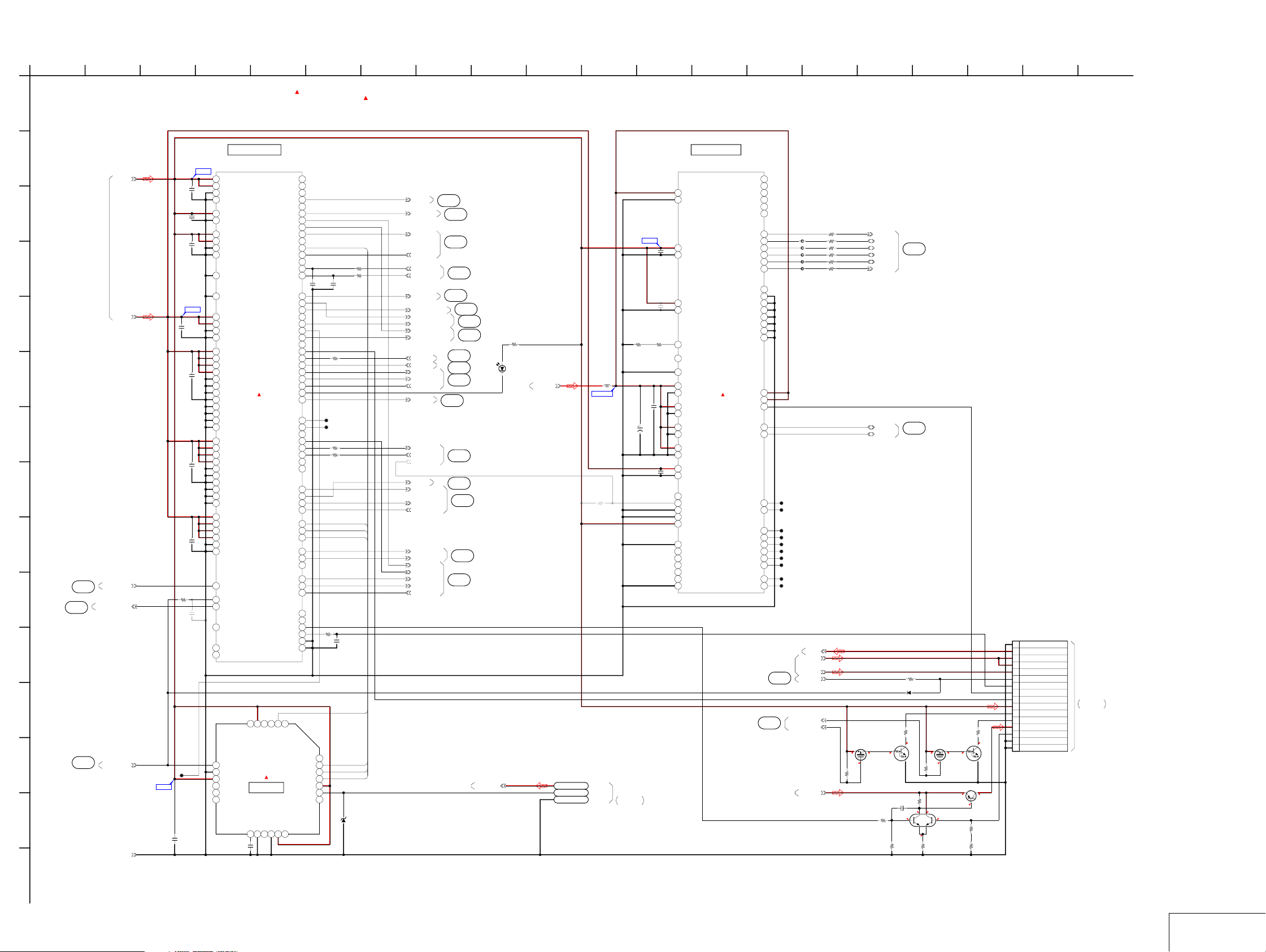
SY-178 (7/8)
Page 15

1
2
SY-178 BOARD(8/8)
A
AUDIO, VIDEO AMP
XX MARK:NO MOUNT
NO MARK:REC/PB MODE
R:REC MODE
P:PB MODE
B
C
D
(4/8)
@043
(3/8)
@019
(3/8)
E
(4/8)
@029
F
G
H
I
J
08
(1/8)
(4/8)
(1/8)
MAX_5.0V
IC211_AUIN
IC211_AUOUT
IC211_CVOUT
XCS_AUDIO
XIC211_2_SCK
IC211_2_SO
AU_AVCC
REG_GND
D_3.0V
A_3.0V
10
MS_PWR_ON
(3/8)
(4/8)
(2/8)
(1/8)
(2/8)
(3/8)
(3/8)
@028
@009
@001
@044
@012
C728
0.1u
C725
22u
6.3V
BOOT_MODE3
BATT_UNREG
(3/8)
(1/8)
IC211_PROUT
IC211_PBOUT
@032
@026
MEMORY STICK LOAD SW
3.1
R757
470k
R756
3300
R755
2200
IC211_1_UO
IC211_1_UI
XPWR_ON
XACV_DET
ACV_UNREG
IC211_YOUT
USB_VBUS
XMS_IN
USB_DP
USB_DM
XACC_IN
Q706
SSM6E01TU
3
0
6
0
R702
0
0
4
5
3.0
1
2
D708
MA2SD32008S0
R602
L601
10uH
XX
C601
4
AU_AVCC
10u
3
R603
0
R604
XX
R601
0
56
:Voltage measurement of the CSP ICs
and the Transistors with mark,are
not possible.
R606
C603
0.0047u
MA2611100AS0
R605
D601
2200
C604
0.1u
10
C605
10u
R614
XX
A6
B6
C6
C5
D6
D5
E6
D4
E5
REC_OUT
PB_IN
VCC_A
GND_D
CS
CLK
DATA
VDD
VDD_PUMP
C606
R607
1u
47k
C608
1u
C607
0.47u
0.01u
C609
A5
C4
B5
AGC_IN
AGC_DET
IC601
AUDIO, VIDEO AMP
CP1
F5
F6
C612
1u
1k
R608
A4
A3
GND_A
MIC_IN
MIC_OUT
IC601
AN12918A-VB
VSSE4VSS_O
CP2F4GND_PUMP
E3
1u
C611
7
0.01u
C610
B4
MIC_REG
VIDEO_IN
F3
1u
C613
B3
R610
1u
C614
10
VREF
A2
VCC_SP
VCC_VD2GND_V
F2
L602
10uH
MAX_5.0V
C617
B2
VREF_SP
VIDEO_OUT
F1
C615
1u
R611
10u
C616
1u
GND_SP
SP_LPF
SP_IN
EVR_OUT
GND_A
MUTE
LINE_OUT
R612
68
D602
MA2611100AS0
1k
SP_+
SP_-
R613
10k
9
8
A1
B1
C1
C2
C3
D3
C619
D1
0.01u
E1
E2
C618
0.47u
@022
(3/8)
LND703
STATIC_GND
LND709
STATIC_GND
R703
0
13
MAZP068H0AS0
C724
(4/8)
(3/8)
D703
3
XX
@021
R743
XX
D702
1
2
@031
(3/8)
@037
1411
C704
0.01u
C729
0.01u
XX
D704
MAZP068H0AS0
1
2
MAZP068H0AS0
MSX_CLK
MSX_D3
MSX_D2
MSX_D0
MSX_D1
MSX_BS
XPWR_LED
XSHUT_SW
XAE_LOCK_SW
R717
R722
R758
R719
SP-
SP+
CN710 30P
ACV_GND
1
ACV_GND
2
ACV_GND
3
XPOWER_ON
4
UART TX
5
UART Rx
6
XACV_DET
7
CHARGE_V
8
CHARGE_V
9
CHARGE_V
10
ACV_UNREG
11
ACV_UNREG
12
ACV_UNREG
13
REG_GND
14
HD Pr
15
REG_GND
16
HD Pb
17
REG_GND
18
USB_VBUS
19
USB_GND
20
USB_DP
21
USB_DM
22
USB_GND
23
AU_LINE_OUT
24
A_GND
25
V_LINE_OUT
26
V_GND
27
HD Y
28
REG_GND
29
XACC_IN
30
CN704
REG_GND
10
MS_VCC
9
MS_CLK
8
MS_D3
7
XMS_IN
6
MS_D2
5
MS_D0
4
MS_D1
3
MS_BS
2
REG_GND
1
CN707 8P
MIC_SIG
1
MIC_GND
2
XPWR_ON
3
X_PWR_LED
4
D_3.0V
5
REG_GND
6
XSHUTTER_SW
7
XAE_LOCK_SW
8
16
LND701
LND702
10P
15
R776
0
1k
LF701
2
4
1
0
0
0
2
3
D705
3
1
R721
0
3
R720
0
1712
SP901
SPEAKER
MC-183
FLEXIBLE
LND101-LND130
PAGE 4-12
of LEVEL2
12
11
RL-076
CN101
PAGE 4-15
of LEVEL2
MEMORY
STICK
DUO
DSC-W200_L3
4-11
SY-178 (8/8)
Page 16

Link
Link
4-3. PRINTED WIRING BOARDS
CD-705 FLEXIBLE BOARD
SY-178 BOARD (SIDE A)
COMMON NOTE FOR PRINTED WIRING BOARDS
SY-178 BOARD (SIDE B)
MOUNTED PARTS LOCATION
DSC-W200_L3
Page 17

4-3. PRINTED WIRING BOARDS
4-3. PRINTED WIRING BOARDS
4-3. PRINTED WIRING BOARDS
THIS NOTE IS COMMON FOR PRINTED WIRING BOARDS
• : Uses unleaded solder.
•
: Circuit board
: Flexible board
Pattern from the side which enables seeing.
: pattern of the rear side
(The other layers’ patterns are not indicated)
• Through hole is omitted.
• There are a few cases that the part printed on diagram
isn’t mounted in this model.
• C : panel designation
• Chip parts.
Tr ansistor Diode
C
EB
654
46
123
3152
21
12
345
534
54
45
123
312
23
14
3
21321321
43
12
4
3
23
14
46
3152
12
31
4625
654
123
DSC-W200_L3
4-16
Page 18

CD-705 (2 layers)
: Uses unleaded solder.
CD-705 FLEXIBLE BOARD
LND045
LND044
LND043
LND042
LND041
LND040
LND039
LND038
LND037
LND036
LND035
LND034
LND033
LND032
LND031
LND030
LND029
LND028
LND027
LND026
LND025
LND024
LND023
LND022
LND021
LND020
LND019
LND018
LND017
LND016
LND015
LND014
LND013
LND012
LND011
LND010
LND009
LND008
LND007
LND006
LND005
LND004
LND003
LND002
LND001
08
C006
R007
R003
C001
4
6
18
20
R006
IC003
13
IC002
21
C003
22
24 36
C008
C007
416
2
1
40
C005
38
CD-705 flexible complete board is not supplied,
Note:
but this is included in CCD block assy.
1-872-136-
11
DSC-W200_L3
4-17
CD-0705
Page 19

SY-178 (8 layers)
: Uses unleaded solder.
SY-178 BOARD (SIDE A)
R543
A
B
C
D
IC501
2.8V
R546
C507
B2B1A2
A1
R721
C566
IC502
R501
R719
R758
R722
D_1.8V
A1
B2B1A2
R544
C510
D703
D704
C548
R503
C511
CL507
CL508
C563
R743
R506R507
R502
C554
CL506
R518
R520
R521
R703
C509
R504R505
CL502
CL501
2.8V
R257
R258
R259
R702
CL503
A3 A4
A1
A2
B3 B4B2
B1
C2
C1
D2
D1
E1
E2
F1
F2
G1
G2
H1
H2
J1
J3 J4J2
K1
R551
8
C556
14
15 21
R260
B
E
E
B
Q243
C
BE
Q244
C
R717
C729
C704
D702
LND703
IC503
D4
E4
F4
G4
R552
29
IC506
R550
C564
2.8V
C
Q242
A5 A6 A7 A8 A9
B5 B6 B7 B8
D6
D7
E7
E5
F7
G5D5G6
G7
J5 J6 J7 J8 J9
K5 K6 K7 K8 K9K2 K3 K4
SE501
(YAW)
3
C552
2.8V
17
28
22
R553
C553
3
C535
R540
4
R261
R262
R776
D705
A10
B10
B9
C10
C9
R516
D10
D9
E10
E9
F10
F9
G10
G9
H10
H9
J10
K10
12
4
C557
C562
C560
R554
C555
C561
C558
SE502
(PITCH)
R723
23
C512
C517
R523
R517
R511
C506
D_3.0V
C513
R512
R513
C503
CL505
R545
R509
R515
A
R522
R519
C549
R514
C514
R510
C516
R508
C266
R406
C406
R408
B
C401
C265
10 1
R539
C536
C565
C547
C559
R555
C537
12
R720
4
X101
1
12
D706
(MS ACCESS)
R610
C616
C614
MAX_5.0V
R608
C609
C604
C610
C612
D602
C617
D201
E4
E5
D4
D5
C4
C5
B4
B5
A4
R611
R603
L602
R604
C205
E3
D3
C3
B3
A3
C201
E2
E1
D2
D1
D_3.0V
C2
C1
B2
B1
A1A5
A2
CL208
CN714
116
R420
C605
D601
AU_AVCC
R614
C615
L601
C613
C611
R605
R601
C601
C608
R602
C606
D_3.0V
C403
R423
CL414
CL415
CL412
CL413
G5
G6
G7
F5
F6
F7
E5
E6
E7
D5
D6
D7
C5
C6
C7
B5
B6
B7
A5
A6
A7
CL402
CL401
CL403
CL406
C724
G4
F4
E4
D4
C4
B4
A4
CL409
G1
G2
G3
F2
F3
F1
E2
E3
E1
D2
D3
D1
C2
C3
C1
B1
B2
B3
A2
A3
A1
CL405
CL404
CL411
R421
R419
IC401
R405
R612
C618
IC601
R607
R613
C619
C607
A1B1C1D1E1F1
A2B2C2D2E2F2
A3B3C3D3E3F3
A4B4C4D4E4F4
A5B5C5D5E5F5
A6B6C6D6E6F6
R606
C603
IC201
C
R731
R732
R734
Q710
BE
C726
R730
46
CN708
R771
12
34
IC702
54
C720
IC701
1
R752
C719
5
C032
610
IC002
1
11
L002
C731
C732
R775
3
CN704
STICK
MEMORY
DUO
11
D707
R701
D
Q711
G
R769
G
S
R770
D708
R756
Q706
13
C728
R757
46
D011
S
46
P
Q014
R074
Q713
BE
Q714
D
Q712
R755
C725
R767
C
C
BE
C033
13
C020
Q704
13
R768
R735
R733
18
R773
C710
C711
B
TI_5.0V
C063
R075
DSC-W200_L3
08
1-871-977-
11
1 2 3 4 5
4-18
SY-178 (SIDE A)
Page 20

SY-178 (8 layers)
: Uses unleaded solder.
SY-178 BOARD (SIDE B)
LND704
LND705
LND706
Note : IC211 is not supplied,
but this is included in SY-178 complete board.
08
1
39
14
F001
R352
C
F002
1
3
Q013
R304
Q302
CN707
D002
D003
Q304
R303
BE
CL327
18
2
CN713
38
58
E
C
B
Q004
C004
R350
R353
R310
46
C301
FB301
R302
C302
R305
D301
C320
R324
C318
C319
C315
C314
TI_5V
CL701
CL702
R763
CL703
R762
CL704
C713
C706
R741
R740
R739
C709
C730
R764
C119
R002
D004
R009
R351
C
Q303
E
B
C305
A
FB302
C308
C303
6
4
IC303
13
C021
C022
D007
C008
C057
C708
R003
A
L303
C310
C349
C309
34
C030
C304
L302
34
R326
IC305
CAM_12V
C016
D006
Q006
G
L702
R321
P
C362
12
IC302
D_3.0V
C348
C321
12
CAM_12V
C027
C044
R024
L004
L003
C013
R015
D
R050
R010
S
R005
45
44
R334
R337
R325
C316
R330
R338
R331
R335
L301
R332
R339
C339
R333
R336
C363
D_3.0V
CL313
C350
C331 CL329
134 133
P3R3 B3 A3
M5P5R5 D5 B5 A5
M6P6R6 D6 B6 A6
M7P7R7 D7 B7 A7
M8P8R8 D8 B8 A8
M9P9R9 D9 B9 A9
M10P10R10 D10 B10 A10
M11P11R11 D11 B11 A11
P13R13 B13 A13
CL315
R344
CL316
C332
C338
CL308
A
C307
45
R328
IC304
123
D010
R030
CAM_-7.5V D_1.2V
R031
24
R049
R042
25
36
37
MAX_5.0V
BL_H
C012
R016
R012
C060
R014
R011
R008
46
Q003
13
L008
IC001
R013
C026
49
C050
C009
C062
C352
C354
C360
H1J1K1L1M1N1P1 G1 F1 E1 D1 C1 B1
H2J2K2L2M2N2P2R2 G2 F2 E2 D2 C2 B2 A2
H4J4K4L4M4P4R4 G4 F4 E4 D4 B4 A4
IC301
H12J12K12L12M12P12R12 G12 F12 E12 D12 B12 A12
H14J14K14L14M14N14P14R14 G14 F14 E14 D14 C14 B14 A14
H15J15K15L15M15N15P15 G15 F15 E15 D15 C15 B15
C335
C340
C334
C342
R341
D_3.0V
R340
FB303
C322
13
48
C010
C028
C046
L009
12
1
C306
CN301
C330
C356
C346
D_1.8V
R018
R017
C011
C326
R347
R301
C015
C351
136135
C327
C034
R028
R029
C024
C048
C014
C357
C358
C355
C353
CL332
CL334
C345
C343
C344
C328
Q301
13
IC007
3452
C061
R019
L006
L005
L007
C361
C359
C329
CL333
CL331
CL330
CL336
CL326
64
CL325
R022
D_3.0V
R306
R307
R308
C324
C325
C241
C213
CL335
CL241
C285
C286
C267
FB282
C216
C229
1
R214
R213
C228
C018
C019
C047
C037
R021
13
Q007
46
R020
AF26AE26AD26AC26AB26AA26Y26W26V26U26T26R26P26N26M26L26K26J26H26G26F26E26D26C26B26A26
13
R241
AF25AE25AD25AC25AB25AA25Y25W25V25U25T25R25P25N25M25L25K25J25H25G25F25E25D25C25B25A25
R228
Q010
R037
R038
Q012
B
2
AF24AE24B24A24
R224
C
L001
C001
1
R254
C247
AF23AE23AC23AB23AA23Y23W23V23U23T23R23P23N23M23L23K23J23H23G23F23E23D23B23A23
AF22AE22AC22AB22AA22Y22W22V22U22T22R22P22N22M22L22K22J22H22G22F22E22D22B22A22
AF21AE21AC21AB21E21D21B21A21
R227
C217
CL219
46
R290
R250
IC003
C035
B2
A2
E
CL107
A_3.0V
R253
R292
AF20AE20AC20AB20Y20W20V20U20T20R20P20N20M20L20K20J20H20G20E20D20B20A20
R104
CL106
CL123
B1
A1
D102
R125
R300
R291
C246
AF19AE19AC19AB19Y19W19V19U19T19R19P19N19M19L19K19J19H19G19E19D19B19A19
CL118
AF18AE18AC18AB18Y18W18H18G18E18D18B18A18
A9
A8
A7
A6
A5
A4
A3
A2
A1
FB255
R293
C248
AF17AE17AC17AB17Y17W17U17T17R17P17N17M17L17K17H17G17E17D17B17A17
AF16AE16AC16AB16Y16W16U16T16R16P16N16M16L16K16H16G16E16D16B16A16
C212
IC103
12
CL122
R103
B9
C9
B8
C8
B7
B6
C6
B5
IC101
B4
C4
B3
B2
C2
B1
C1
CL101
51
50
L241
AF15AE15AC15AB15Y15W15U15T15L15K15H15G15E15D15B15A15
AF14AE14AC14AB14Y14W14U14T14L14K14H14G14E14D14B14A14
IC211
C242
R110
CL124
D9
E9
D8
E8
D7
D3
D2
E2
D1
E1
CL120
CL119
R266
C245
AF13AE13AC13AB13Y13W13U13T13L13K13H13G13E13D13B13A13
AF12AE12AC12AB12Y12W12U12T12L12K12H12G12E12D12B12A12
D_3.0V
R212
C220
1
34
C117
R109
F9
G9
F8
G8
F7
G6
G4
F3
F2
G2
F1
G1
C107
C251
C252
R268
C253
AF11AE11AC11AB11Y11W11U11T11R11P11N11M11L11K11H11G11E11D11B11A11
FB234
R222
FB233
C105
H9
H8
H7
H6
H5
H4
H3
H2
H1
R221
R121
R106
1
CN402
A
B
C
D
R418
R401
R402
Q401
R225
R280
R273
R267
R274
AF10AE10AC10AB10Y10W10U10T10R10P10N10M10L10K10H10G10E10D10B10A10
R217
R219
J9
J8
J7
J6
J5
J4
J3
J2
J1
C261
C256
AF9AE9AC9AB9Y9W9H9G9E9D9B9A9
C106
R271
FB230
R218
FB231
R289
R270
R269
R263
AF8AE8AC8AB8Y8W8V8U8T8R8P8N8M8L8K8J8H8G8E8D8B8A8
C225
CL218
CL215
R220
R120
C116
D_1.8V
AF7AE7AC7AB7Y7W7V7U7T7R7P7N7M7L7K7J7H7G7E7D7B7A7
CL216
CL217
FB232
CL113
R113
R112
R108
C243
R281
C257
CL212
CL214
CL211
CL110
C227
R272
R264
AF6AE6AC6AB6E6D6B6A6
CL111
CL109
C113
C112
R107
R203
C
E
B
C206
C263
C264
R295
R294
R296
R298
R276
R279
R299
R275
C254
C260
R297
R265
AF5AE5AC5AB5AA5Y5W5V5U5T5R5P5N5M5L5K5J5H5G5F5E5D5B5A5
AF4AE4AC4AB4AA4Y4W4V4U4T4R4P4N4M4L4K4J4H4G4F4E4D4B4A4
AF3AE3B3A3
AF2AE2AD2AC2AB2AA2Y2W2V2U2T2R2P2N2M2L2K2J2H2G2F2E2D2C2B2A2
AF1AE1AD1AC1AB1AA1Y1W1V1U1T1R1P1N1M1L1K1J1H1G1F1E1D1C1B1A1
R226
C281
CL222
VL_3V
CL213
C114
R116
4
CL112
IC102
C109
58
R114
C110
A
C104
C103
X201
C259
C214
C223
R216
C224
C215
D_3.0V D_1.2V
C211
CL220
C262
C226
FB283
C282
C284
C283
FB281
R119
R102
R118
R117
1
BACK_UP_VCC
R126
R211
C208
C249
C222
CAM_3.5V
CL221
C287
13
Q101
D101
EVER_3.0V
C111
LND709
R215
C207
LF701
R105
C108
R206
1
IC202
4
R209
13
L211
C250
L242
12
34
46
8
9
5
C202
R256
Q241
1 30
1-871-977-
C204
R210
P
R205
46
C203
CN710
R204
2
R412
R411
LND702
SP901
SPEAKER
LND701
11
DSC-W200_L3
4-19
12345
SY-178 (SIDE B)
Page 21

4-3. PRINTED WIRING BOARDS
4-3. PRINTED WIRING BOARDS
4-4. MOUNTED PARTS LOCATION
SY-178 BOARD
* C001 D-3
* C004 A-5
* C008 D-4
* C009 D-3
* C010 D-3
* C011 D-3
* C012 D-4
* C013 D-4
* C014 D-3
* C015 D-3
* C016 C-4
* C018 C-3
* C019 C-3
C020 D-5
* C021 C-4
* C022 C-4
* C024 C-3
* C026 C-3
* C027 C-4
* C028 B-3
* C030 C-4
C032 C-5
C033 C-5
* C034 B-3
* C035 D-3
* C037 C-3
* C044 C-4
* C046 C-3
* C047 C-3
* C048 D-3
* C050 D-3
* C057 D-4
* C060 D-4
* C061 C-3
* C062 D-4
C063 D-5
* C103 D-2
* C104 D-2
* C105 D-2
* C106 D-2
* C107 D-2
* C108 D-1
* C109 D-2
* C110 D-1
* C111 D-1
* C112 D-2
* C113 D-2
* C114 C-2
* C116 D-2
* C117 D-2
* C119 D-5
C201 A-4
* C202 A-1
* C203 A-1
* C204 A-1
C205 A-4
* C206 A-2
* C207 A-1
* C208 B-1
* C211 B-1
* C212 C-2
* C213 B-3
* C214 B-1
* C215 B-1
* C216 B-3
* C217 C-3
* C220 C-2
* C222 B-1
* C223 B-1
* C224 B-1
* C225 C-2
* C226 C-1
* C227 A-2
* C228 C-3
* C229 B-3
* C241 A-3
* C242 C-2
* C243 A-2
* C245 B-2
* C246 B-2
* C247 B-3
* C248 B-2
* C249 B-1
* C250 B-1
* C251 A-2
* C252 A-2
* C253 B-2
* C254 B-2
* C256 B-2
* C257 B-2
* C259 B-1
* C260 B-2
* C261 A-2
* C262 B-1
* C263 A-2
* C264 A-2
C265 A-2
C266 A-2
* C267 B-3
* C281 C-2
* C282 C-1
* C283 C-1
* C284 C-1
* C285 B-3
* C286 B-3
* C287 C-1
* C301 B-5
* C302 B-5
* C303 B-4
* C304 A-4
* C305 B-4
* C306 B-4
* C307 B-3
* C308 B-4
* C309 B-4
* C310 A-4
* C314 C-5
* C315 B-5
* C316 B-4
* C318 B-5
* C319 B-5
* C320 B-5
* C321 C-4
* C322 B-3
* C324 A-3
* C325 A-3
* C326 B-3
* C327 B-3
* C328 B-3
* C329 A-3
* C330 A-3
* C331 A-4
* C332 B-4
* C334 B-3
* C335 B-3
* C338 B-4
* C339 A-4
* C340 B-3
* C342 B-3
* C343 B-3
* C344 B-3
* C345 B-3
* C346 B-3
* C348 B-4
* C349 A-4
* C350 A-4
* C351 A-3
* C352 A-3
* C353 A-3
* C354 A-3
* C355 A-3
* C356 A-3
* C357 A-3
* C358 A-3
* C359 A-3
* C360 A-4
* C361 A-3
* C362 B-4
* C363 B-4
C401 A-2
C403 A-3
C406 A-2
C503 A-2
C506 A-2
C507 A-1
C509 A-1
C510 A-1
C511 A-1
C512 A-2
C513 A-2
C514 A-2
C516 A-2
C517 A-2
C535 C-1
C536 B-2
C537 C-2
C547 B-2
C548 A-1
C549 A-2
C552 B-1
C553 C-1
C554 A-1
C555 B-2
C556 B-1
C557 B-2
C558 B-2
C559 B-2
C560 B-2
C561 B-2
C562 B-2
C563 B-1
C564 B-1
C565 B-2
C566 A-1
C601 A-3
C603 A-4
C604 A-4
C605 A-3
C606 A-4
C607 A-4
C608 A-3
C609 A-4
C610 A-4
C611 A-3
C612 A-4
C613 A-3
C614 A-4
C615 A-3
C616 A-4
C617 A-4
C618 A-4
C619 A-4
C704 D-1
* C706 C-5
* C708 D-4
* C709 D-5
C710 C-5
C711 C-5
* C713 C-5
C719 C-5
C720 C-5
C724 A-2
C725 C-4
C726 B-5
C728 C-4
C729 D-1
* C730 D-5
C731 C-5
C732 C-5
* CL101 D-2
* CL106 D-2
* CL107 D-2
* CL109 D-2
* CL110 D-2
* CL111 D-2
* CL112 D-2
* CL113 D-2
* CL118 D-2
* CL119 D-2
* CL120 D-2
* CL122 D-2
* CL123 D-2
* CL124 D-2
CL208 B-4
* CL211 C-2
* CL212 C-2
* CL213 C-2
* CL214 C-2
* CL215 C-2
* CL216 C-2
* CL217 C-2
* CL218 C-2
* CL219 C-3
* CL220 B-1
* CL221 B-1
* CL222 C-2
* CL241 B-3
* CL308 B-4
* CL313 B-4
* CL315 B-4
* CL316 B-4
* CL325 B-3
* CL326 B-3
* CL327 B-5
* CL329 A-4
* CL330 B-3
* CL331 B-3
* CL332 A-3
* CL333 A-3
* CL334 B-3
* CL335 B-3
* CL336 B-3
CL401 A-3
CL402 A-3
CL403 A-2
CL404 A-3
CL405 A-3
CL406 A-3
CL409 A-3
CL411 A-3
CL412 A-3
CL413 A-2
CL414 A-3
CL415 A-3
CL501 A-1
CL502 B-1
CL503 A-1
CL505 A-2
CL506 A-1
CL507 A-1
CL508 A-1
* CL701 C-5
* CL702 C-5
* CL703 C-5
* CL704 C-5
* CN301 A-3
* CN402 A-2
CN704 D-3
* CN707 B-5
CN708 B-5
* CN710 C-1
* CN713 C-5
CN714 A-5
* D002 A-5
* D003 A-5
* D004 A-4
* D006 D-4
* D007 D-4
* D010 C-4
D011 D-4
* D101 C-1
* D102 D-2
D201 A-4
* D301 B-5
D601 A-3
D602 A-4
D702 D-1
D703 D-1
D704 D-1
D705 D-1
D706 D-2
D707 B-4
D708 C-4
* F001 A-5
* F002 A-5
* FB230 C-2
* FB231 C-2
* FB232 C-2
* FB233 C-2
* FB234 C-2
* FB255 A-2
* FB281 C-1
* FB282 B-3
* FB283 C-1
* FB301 B-5
* FB302 B-5
* FB303 B-3
* IC001 C-4
IC002 C-5
* IC003 D-2
* IC007 B-3
* IC101 D-2
* IC102 D-2
* IC103 C-2
IC201 B-4
* IC202 A-1
* IC211 B-2
* IC301 B-3
* IC302 B-4
* IC303 B-4
* IC304 B-4
* IC305 C-4
IC401 A-3
IC501 A-1
IC502 A-1
IC503 A-1
IC506 B-1
IC601 A-4
IC701 C-5
IC702 C-5
* L001 D-3
L002 D-5
* L003 D-4
* L004 C-4
* L005 C-3
* L006 C-3
* L007 D-3
* L008 C-4
* L009 C-3
* L211 B-1
* L241 A-2
* L242 B-1
* L301 B-4
* L302 B-4
* L303 A-4
L601 A-3
L602 A-4
* L702 D-4
* LF701 C-1
* LND701 B-1
* LND702 B-1
LND703 D-1
* LND704 A-4
* LND705 A-4
* LND706 A-5
* LND709 D-1
* Q003 D-4
* Q004 A-5
* Q006 D-4
* Q007 D-3
* Q010 C-3
* Q012 D-3
* Q013 A-5
Q014 D-4
* Q101 C-1
* Q241 B-1
Q242 C-1
Q243 C-1
Q244 D-1
* Q301 B-3
* Q302 B-5
* Q303 A-4
* Q304 B-5
* Q401 A-2
Q704 B-5
Q706 C-4
Q710 B-5
Q711 B-4
Q712 B-4
Q713 B-4
no mark : side A
mark : side B
*
Q714 B-5
* R002 A-4
* R003 A-4
* R005 D-4
* R008 D-4
* R009 A-4
* R010 D-4
* R011 D-4
* R012 D-4
* R013 D-4
* R014 D-4
* R015 D-4
* R016 D-4
* R017 D-3
* R018 D-3
* R019 C-3
* R020 D-3
* R021 C-3
* R022 C-3
* R024 C-4
* R028 C-3
* R029 C-3
* R030 C-4
* R031 C-4
* R037 D-3
* R038 D-3
* R042 C-4
* R049 C-4
* R050 D-4
R074 D-4
R075 D-5
* R102 C-1
* R103 D-2
* R104 D-3
* R105 C-1
* R106 D-2
* R107 D-2
* R108 D-2
* R109 D-2
* R110 D-2
* R112 D-2
* R113 D-2
* R114 D-2
* R116 C-2
* R117 C-1
* R118 C-2
* R119 C-1
* R120 D-2
* R121 D-2
* R125 D-2
* R126 D-1
* R203 A-2
* R204 A-1
* R205 B-1
* R206 A-1
* R209 B-1
* R210 A-1
* R211 A-1
* R212 C-2
* R213 C-3
* R214 C-3
* R215 B-1
* R216 B-1
* R217 C-2
* R218 C-2
* R219 C-2
* R220 C-2
* R221 C-2
* R222 C-2
* R224 C-3
* R225 A-2
* R226 C-2
* R227 C-3
* R228 C-3
* R241 A-3
* R250 D-3
* R253 A-3
* R254 A-3
* R256 B-1
R257 C-1
R258 C-1
R259 D-1
R260 C-1
DSC-W200_L3
4-24
SY-178
Page 22

4-3. PRINTED WIRING BOARDS
4-3. PRINTED WIRING BOARDS
no mark : side A
mark : side B
*
R261 C-1
R262 D-1
* R263 B-2
* R264 B-2
* R265 B-2
* R266 A-2
* R267 A-2
* R268 A-2
* R269 A-2
* R270 A-2
* R271 A-2
* R272 B-2
* R273 A-2
* R274 A-2
* R275 B-2
* R276 A-2
* R279 A-2
* R280 A-2
* R281 A-2
* R289 A-2
* R290 C-3
* R291 A-2
* R292 A-2
* R293 A-2
* R294 A-2
* R295 A-2
* R296 A-2
* R297 B-2
* R298 A-2
* R299 B-2
* R300 A-2
* R301 B-3
* R302 B-5
* R303 B-5
* R304 B-5
* R305 B-5
* R306 A-3
* R307 A-3
* R308 A-3
* R310 B-5
* R321 B-4
* R324 B-5
* R325 B-4
* R326 B-4
* R328 B-4
* R330 A-4
* R331 B-4
* R332 A-4
* R333 B-4
* R334 B-4
* R335 B-4
* R336 B-4
* R337 B-4
* R338 A-4
* R339 A-4
* R340 B-3
* R341 B-3
* R344 B-4
* R347 B-3
* R350 A-5
* R351 A-4
* R352 B-5
* R353 B-5
* R401 A-2
* R402 A-2
R405 A-3
R406 A-2
R408 A-2
* R411 A-1
* R412 A-1
* R418 A-2
R419 A-3
R420 A-3
R421 A-3
R423 A-3
R501 A-1
R502 A-1
R503 A-1
R504 A-1
R505 A-1
R506 A-1
R507 A-1
R508 A-2
R509 A-2
R510 A-2
R511 A-2
R512 A-2
R513 A-2
R514 A-2
R515 A-2
R516 A-2
R517 A-2
R518 A-1
R519 A-2
R520 A-1
R521 A-1
R522 A-2
R523 A-2
R539 B-2
R540 C-1
R543 A-1
R544 A-1
R545 A-2
R546 A-1
R550 B-1
R551 B-1
R552 B-1
R553 B-1
R554 B-2
R555 B-2
R601 A-3
R602 A-4
R603 A-4
R604 A-4
R605 A-3
R606 A-4
R607 A-4
R608 A-4
R610 A-4
R611 A-4
R612 A-4
R613 A-4
R614 A-3
R701 B-4
R702 D-1
R703 D-1
R717 D-1
R719 C-1
R720 C-2
R721 D-1
R722 C-1
R723 D-2
R730 B-5
R731 B-5
R732 B-5
R733 B-5
R734 B-5
R735 B-5
* R739 D-5
* R740 D-5
* R741 D-5
R743 D-1
R752 C-5
R755 C-4
R756 C-4
R757 C-4
R758 C-1
* R762 C-5
* R763 C-5
* R764 D-5
R767 B-5
R768 B-5
R769 B-4
R770 C-4
R771 C-5
R773 C-5
R775 C-5
R776 D-1
SE501 B-2
SE502 C-2
X101 D-2
* X201 A-1
DSC-W200_L3
4-25
SY-178
Page 23

5. REPAIR PARTS LIST
NOTE:
• -XX, -X mean standardized parts, so they may have some differences from
the original one.
• Items marked “*” are not stocked since they are seldom required for routine
service. Some delay should be anticipated when ordering these items.
• The mechanical parts with no reference number in the exploded views are not
supplied.
• Due to standardization, replacements in the parts list may be different from
the parts specified in the diagrams or the components used on the set.
• CAPACITORS:
uF: µF
• COILS
uH: µH
• RESISTORS
All resistors are in ohms.
METAL: metal-film resistor
METAL OXIDE: Metal Oxide-film resistor
F: nonflammable
• SEMICONDUCTORS
In each case, u: µ, for example:
uA...: µA... , uPA... , µPA... ,
uPB... , µPB... , µPC... , µPC... ,
uPD..., µPD...
• Abbreviation
AR : Argentine model
AUS: Australian model
BR : Brazilian model
CH : Chinese model
CND : Canadian model
EE : East European model
HK : Hong Kong model
J: Japanese model
JE : Tourist model
KR : Korea model
NE : North European model
TW : Taiwan model
When indicating parts by reference number,
please include the board name.
The components identified by mark 0 or
dotted line with mark 0 are critical for safety.
Replace only with part number specified.
Les composants identifiés par une marque
0 sont critiques pour la sécurité.
Ne les remplacer que par une pièce portant
le numéro spécifié.
DSC-W200_L3
5-1
Page 24

CD-705
5-2. ELECTRICAL PARTS LIST
Ref. No. Part No. Description Ref. No. Part No. Description
A-1234-356-A CCD BLOCK ASSY (Note)
(Not supplied) CD-705 FLEXIBLE BOARD
(CD-705 flexible complete board is not supplied, but this is included in CCD
C001 1-164-943-11 CERAMIC CHIP 0.01uF 10% 16V
C003 1-127-715-11 CERAMIC CHIP 0.22uF 10% 16V
C005 1-125-777-11 CERAMIC CHIP 0.1uF 10% 10V
C006 1-164-943-11 CERAMIC CHIP 0.01uF 10% 16V
C007 1-100-505-11 CERAMIC CHIP 0.1uF 20% 16V
C008 1-127-715-11 CERAMIC CHIP 0.22uF 10% 16V
IC002 8-753-230-85 IC CXA3691EN-T9
* IC003 8-753-272-28 IC ICX612CQZ-13
R003 1-218-981-81 RES-CHIP 220K 5% 1/16W
R006 1-218-990-11 SHORT CHIP 0
R007 1-208-941-11 METAL CHIP 180K 0.5% 1/16W
************************************************************
*********************
block assy.)
< CAPACITOR >
< IC >
< RESISTOR >
DSC-W200_L3
Note: Be sure to read “Precautions for Replacement of
Imager” on page 4-2 when changing the imager.
5-8
Page 25

SY-178
Ref. No. Part No. Description Ref. No. Part No. Description
A-1283-757-A SY-178 BOARD, COMPLETE (SERVICE)
*******************************
(IC211 is not supplied, but this is included in SY-178 complete board.)
< CAPACITOR >
C001 1-100-611-91 CERAMIC CHIP 22uF 20% 6.3V
C004 1-112-717-91 CERAMIC CHIP 1uF 10% 6.3V
C008 1-100-671-11 CERAMIC CHIP 4.7uF 20% 25V
C009 1-100-881-91 CERAMIC CHIP 47uF 20% 6.3V
C010 1-100-611-91 CERAMIC CHIP 22uF 20% 6.3V
C011 1-100-611-91 CERAMIC CHIP 22uF 20% 6.3V
C012 1-165-887-91 CERAMIC CHIP 0.22uF 10% 6.3V
C013 1-165-908-11 CERAMIC CHIP 1uF 10% 10V
C014 1-165-989-11 CERAMIC CHIP 10uF 10% 6.3V
C015 1-165-908-11 CERAMIC CHIP 1uF 10% 10V
C016 1-165-908-11 CERAMIC CHIP 1uF 10% 10V
C018 1-165-908-11 CERAMIC CHIP 1uF 10% 10V
C019 1-100-611-91 CERAMIC CHIP 22uF 20% 6.3V
C020 1-100-159-91 CERAMIC CHIP 22uF 10% 6.3V
C021 1-100-672-11 CERAMIC CHIP 10uF 20% 16V
C022 1-100-672-11 CERAMIC CHIP 10uF 20% 16V
C024 1-165-989-11 CERAMIC CHIP 10uF 10% 6.3V
C026 1-165-908-11 CERAMIC CHIP 1uF 10% 10V
C027 1-100-670-11 CERAMIC CHIP 4.7uF 20% 16V
C028 1-100-611-91 CERAMIC CHIP 22uF 20% 6.3V
C030 1-100-670-11 CERAMIC CHIP 4.7uF 20% 16V
C032 1-165-884-91 CERAMIC CHIP 2.2uF 10% 6.3V
* C033 1-112-662-91 TANTAL. CHIP 47uF 20% 10V
C034 1-125-777-11 CERAMIC CHIP 0.1uF 10% 10V
* C035 1-112-746-11 CERAMIC CHIP 4.7uF 10% 6.3V
C044 1-100-670-11 CERAMIC CHIP 4.7uF 20% 16V
C046 1-100-611-91 CERAMIC CHIP 22uF 20% 6.3V
C047 1-100-611-91 CERAMIC CHIP 22uF 20% 6.3V
C048 1-165-989-11 CERAMIC CHIP 10uF 10% 6.3V
C050 1-100-881-91 CERAMIC CHIP 47uF 20% 6.3V
C057 1-100-671-11 CERAMIC CHIP 4.7uF 20% 25V
C060 1-165-887-91 CERAMIC CHIP 0.22uF 10% 6.3V
C061 1-112-716-11 CERAMIC CHIP 0.1uF B (0603)
C062 1-165-989-11 CERAMIC CHIP 10uF 10% 6.3V
C063 1-100-581-81 CERAMIC CHIP 0.0047uF 10% 50V
C103 1-125-777-11 CERAMIC CHIP 0.1uF 10% 10V
C104 1-100-567-81 CERAMIC CHIP 0.01uF 10% 25V
C105 1-119-923-11 CERAMIC CHIP 0.047uF 10% 10V
C106 1-125-777-11 CERAMIC CHIP 0.1uF 10% 10V
C107 1-125-777-11 CERAMIC CHIP 0.1uF 10% 10V
C109 1-100-581-81 CERAMIC CHIP 0.0047uF 10% 50V
C110 1-100-842-91 TANTAL. CHIP 47uF 20% 6.3V
C111 1-125-777-11 CERAMIC CHIP 0.1uF 10% 10V
C112 1-164-852-11 CERAMIC CHIP 12PF 5% 50V
C113 1-164-852-11 CERAMIC CHIP 12PF 5% 50V
C114 1-164-939-11 CERAMIC CHIP 0.0022uF 10% 50V
C116 1-125-777-11 CERAMIC CHIP 0.1uF 10% 10V
C117 1-112-716-11 CERAMIC CHIP 0.1uF B (0603)
C119 1-128-628-11 CERAMIC CHIP 0.0022uF 10% 6.3V
C201 1-125-777-11 CERAMIC CHIP 0.1uF 10% 10V
C202 1-125-926-11 TANTAL. CHIP 4.7uF 20% 6.3V
C203 1-125-777-11 CERAMIC CHIP 0.1uF 10% 10V
C204 1-125-777-11 CERAMIC CHIP 0.1uF 10% 10V
C205 1-112-717-91 CERAMIC CHIP 1uF 10% 6.3V
C206 1-125-777-11 CERAMIC CHIP 0.1uF 10% 10V
C211 1-125-777-11 CERAMIC CHIP 0.1uF 10% 10V
C212 1-125-777-11 CERAMIC CHIP 0.1uF 10% 10V
C213 1-125-777-11 CERAMIC CHIP 0.1uF 10% 10V
C214 1-125-777-11 CERAMIC CHIP 0.1uF 10% 10V
C215 1-125-777-11 CERAMIC CHIP 0.1uF 10% 10V
C216 1-125-777-11 CERAMIC CHIP 0.1uF 10% 10V
C217 1-125-777-11 CERAMIC CHIP 0.1uF 10% 10V
C220 1-125-777-11 CERAMIC CHIP 0.1uF 10% 10V
C222 1-100-962-91 TANTAL. CHIP 22uF 20% 6.3V
C223 1-125-777-11 CERAMIC CHIP 0.1uF 10% 10V
C224 1-125-777-11 CERAMIC CHIP 0.1uF 10% 10V
C225 1-125-777-11 CERAMIC CHIP 0.1uF 10% 10V
C228 1-100-965-91 CERAMIC CHIP 0.047uF 10% 6.3V
C229 1-100-965-91 CERAMIC CHIP 0.047uF 10% 6.3V
C241 1-125-777-11 CERAMIC CHIP 0.1uF 10% 10V
C242 1-125-777-11 CERAMIC CHIP 0.1uF 10% 10V
C243 1-125-777-11 CERAMIC CHIP 0.1uF 10% 10V
C245 1-165-989-11 CERAMIC CHIP 10uF 10% 6.3V
C246 1-100-611-91 CERAMIC CHIP 22uF 20% 6.3V
C247 1-100-611-91 CERAMIC CHIP 22uF 20% 6.3V
C248 1-100-611-91 CERAMIC CHIP 22uF 20% 6.3V
C249 1-100-611-91 CERAMIC CHIP 22uF 20% 6.3V
C250 1-165-989-11 CERAMIC CHIP 10uF 10% 6.3V
C251 1-125-777-11 CERAMIC CHIP 0.1uF 10% 10V
C252 1-125-777-11 CERAMIC CHIP 0.1uF 10% 10V
C253 1-125-777-11 CERAMIC CHIP 0.1uF 10% 10V
C254 1-125-777-11 CERAMIC CHIP 0.1uF 10% 10V
C256 1-125-777-11 CERAMIC CHIP 0.1uF 10% 10V
C257 1-125-777-11 CERAMIC CHIP 0.1uF 10% 10V
C259 1-125-777-11 CERAMIC CHIP 0.1uF 10% 10V
C260 1-125-777-11 CERAMIC CHIP 0.1uF 10% 10V
C261 1-125-777-11 CERAMIC CHIP 0.1uF 10% 10V
C262 1-125-777-11 CERAMIC CHIP 0.1uF 10% 10V
C263 1-164-937-11 CERAMIC CHIP 0.001uF 10% 50V
C264 1-164-937-11 CERAMIC CHIP 0.001uF 10% 50V
C265 1-164-937-11 CERAMIC CHIP 0.001uF 10% 50V
C266 1-164-937-11 CERAMIC CHIP 0.001uF 10% 50V
C267 1-112-716-11 CERAMIC CHIP 0.1uF B (0603)
C281 1-125-777-11 CERAMIC CHIP 0.1uF 10% 10V
C282 1-125-777-11 CERAMIC CHIP 0.1uF 10% 10V
C283 1-125-777-11 CERAMIC CHIP 0.1uF 10% 10V
C284 1-125-777-11 CERAMIC CHIP 0.1uF 10% 10V
C285 1-125-777-11 CERAMIC CHIP 0.1uF 10% 10V
C286 1-125-777-11 CERAMIC CHIP 0.1uF 10% 10V
C287 1-100-611-91 CERAMIC CHIP 22uF 20% 6.3V
C301 1-137-701-11 TANTAL. CHIP 4.7uF 20% 10V
C302 1-100-566-91 CERAMIC CHIP 0.1uF 10% 25V
C303 1-100-591-91 CERAMIC CHIP 1uF 10% 25V
C304 1-100-670-11 CERAMIC CHIP 4.7uF 20% 16V
C305 1-100-844-91 TANTAL. CHIP 22uF 20% 10V
C306 1-100-670-11 CERAMIC CHIP 4.7uF 20% 16V
C307 1-100-842-91 TANTAL. CHIP 47uF 20% 6.3V
C308 1-164-939-11 CERAMIC CHIP 0.0022uF 10% 50V
C309 1-100-842-91 TANTAL. CHIP 47uF 20% 6.3V
C310 1-107-826-11 CERAMIC CHIP 0.1uF 10% 16V
DSC-W200_L3
5-10
Page 26

Ref. No. Part No. Description Ref. No. Part No. Description
C314 1-165-908-11 CERAMIC CHIP 1uF 10% 10V
C315 1-165-989-11 CERAMIC CHIP 10uF 10% 6.3V
C316 1-112-717-91 CERAMIC CHIP 1uF 10% 6.3V
C318 1-112-717-91 CERAMIC CHIP 1uF 10% 6.3V
C319 1-100-567-81 CERAMIC CHIP 0.01uF 10% 25V
C320 1-100-611-91 CERAMIC CHIP 22uF 20% 6.3V
* C321 1-112-298-91 CERAMIC CHIP 1uF 10% 16V
* C322 1-112-298-91 CERAMIC CHIP 1uF 10% 16V
C324 1-107-826-11 CERAMIC CHIP 0.1uF 10% 16V
C325 1-107-826-11 CERAMIC CHIP 0.1uF 10% 16V
C326 1-164-937-11 CERAMIC CHIP 0.001uF 10% 50V
C328 1-112-716-11 CERAMIC CHIP 0.1uF B (0603)
C329 1-100-505-11 CERAMIC CHIP 0.1uF 20% 16V
C330 1-125-777-11 CERAMIC CHIP 0.1uF 10% 10V
C331 1-112-716-11 CERAMIC CHIP 0.1uF B (0603)
C332 1-112-716-11 CERAMIC CHIP 0.1uF B (0603)
C334 1-112-716-11 CERAMIC CHIP 0.1uF B (0603)
C335 1-112-716-11 CERAMIC CHIP 0.1uF B (0603)
C338 1-112-716-11 CERAMIC CHIP 0.1uF B (0603)
C339 1-112-716-11 CERAMIC CHIP 0.1uF B (0603)
C340 1-112-716-11 CERAMIC CHIP 0.1uF B (0603)
C342 1-112-716-11 CERAMIC CHIP 0.1uF B (0603)
C343 1-112-716-11 CERAMIC CHIP 0.1uF B (0603)
C344 1-125-777-11 CERAMIC CHIP 0.1uF 10% 10V
C345 1-125-777-11 CERAMIC CHIP 0.1uF 10% 10V
C349 1-112-298-91 CERAMIC CHIP 1uF 10% 16V
C362 1-112-816-91 TANTAL. CHIP 22uF 20% 4V
C401 1-100-663-11 TANTAL. CHIP 22uF 20% 10V
C403 1-125-777-11 CERAMIC CHIP 0.1uF 10% 10V
C503 1-125-777-11 CERAMIC CHIP 0.1uF 10% 10V
C505 1-100-844-91 TANTAL. CHIP 22uF 20% 10V
C506 1-125-777-11 CERAMIC CHIP 0.1uF 10% 10V
C507 1-125-777-11 CERAMIC CHIP 0.1uF 10% 10V
C509 1-100-567-81 CERAMIC CHIP 0.01uF 10% 25V
C510 1-164-939-11 CERAMIC CHIP 0.0022uF 10% 50V
C511 1-100-567-81 CERAMIC CHIP 0.01uF 10% 25V
C513 1-100-567-81 CERAMIC CHIP 0.01uF 10% 25V
C514 1-164-939-11 CERAMIC CHIP 0.0022uF 10% 50V
C516 1-100-567-81 CERAMIC CHIP 0.01uF 10% 25V
C535 1-125-777-11 CERAMIC CHIP 0.1uF 10% 10V
C536 1-125-777-11 CERAMIC CHIP 0.1uF 10% 10V
C537 1-125-777-11 CERAMIC CHIP 0.1uF 10% 10V
C547 1-165-989-11 CERAMIC CHIP 10uF 10% 6.3V
C552 1-112-716-11 CERAMIC CHIP 0.1uF B (0603)
C553 1-112-716-11 CERAMIC CHIP 0.1uF B (0603)
C555 1-112-716-11 CERAMIC CHIP 0.1uF B (0603)
C556 1-112-716-11 CERAMIC CHIP 0.1uF B (0603)
C557 1-165-989-11 CERAMIC CHIP 10uF 10% 6.3V
C558 1-165-989-11 CERAMIC CHIP 10uF 10% 6.3V
C559 1-100-965-91 CERAMIC CHIP 0.047uF 10% 6.3V
C560 1-100-965-91 CERAMIC CHIP 0.047uF 10% 6.3V
C561 1-100-965-91 CERAMIC CHIP 0.047uF 10% 6.3V
C562 1-100-965-91 CERAMIC CHIP 0.047uF 10% 6.3V
* C563 1-112-746-11 CERAMIC CHIP 4.7uF 10% 6.3V
* C564 1-112-746-11 CERAMIC CHIP 4.7uF 10% 6.3V
C565 1-125-777-11 CERAMIC CHIP 0.1uF 10% 10V
C566 1-100-415-11 CERAMIC CHIP 0.47uF 10% 6.3V
C601 1-165-989-11 CERAMIC CHIP 10uF 10% 6.3V
C603 1-100-581-81 CERAMIC CHIP 0.0047uF 10% 50V
C604 1-125-777-11 CERAMIC CHIP 0.1uF 10% 10V
C605 1-165-989-11 CERAMIC CHIP 10uF 10% 6.3V
C606 1-165-908-11 CERAMIC CHIP 1uF 10% 10V
C607 1-100-415-11 CERAMIC CHIP 0.47uF 10% 6.3V
C608 1-165-908-11 CERAMIC CHIP 1uF 10% 10V
C609 1-100-567-81 CERAMIC CHIP 0.01uF 10% 25V
C610 1-100-567-81 CERAMIC CHIP 0.01uF 10% 25V
C611 1-165-908-11 CERAMIC CHIP 1uF 10% 10V
C612 1-165-908-11 CERAMIC CHIP 1uF 10% 10V
C613 1-165-908-11 CERAMIC CHIP 1uF 10% 10V
C614 1-165-908-11 CERAMIC CHIP 1uF 10% 10V
C615 1-165-908-11 CERAMIC CHIP 1uF 10% 10V
C616 1-165-908-11 CERAMIC CHIP 1uF 10% 10V
C617 1-165-989-11 CERAMIC CHIP 10uF 10% 6.3V
C618 1-100-415-11 CERAMIC CHIP 0.47uF 10% 6.3V
C619 1-100-567-81 CERAMIC CHIP 0.01uF 10% 25V
C704 1-100-567-81 CERAMIC CHIP 0.01uF 10% 25V
C706 1-165-989-11 CERAMIC CHIP 10uF 10% 6.3V
C708 1-100-966-91 CERAMIC CHIP 10uF 20% 10V
C709 1-127-760-11 CERAMIC CHIP 4.7uF 10% 6.3V
C710 1-100-415-11 CERAMIC CHIP 0.47uF 10% 6.3V
C711 1-107-826-11 CERAMIC CHIP 0.1uF 10% 16V
C713 1-125-889-11 CERAMIC CHIP 2.2uF 10% 10V
C725 1-100-786-91 TANTAL. CHIP 22uF 20% 6.3V
C726 1-164-931-11 CERAMIC CHIP 100PF 10% 50V
C728 1-125-777-11 CERAMIC CHIP 0.1uF 10% 10V
C729 1-100-567-81 CERAMIC CHIP 0.01uF 10% 25V
C730 1-125-777-11 CERAMIC CHIP 0.1uF 10% 10V
C731 1-165-908-11 CERAMIC CHIP 1uF 10% 10V
C732 1-100-415-11 CERAMIC CHIP 0.47uF 10% 6.3V
< CONNECTOR >
* CN301 1-817-910-71 CONNECTOR, FPC (ZIF) 45P
* CN402 1-817-283-71 CONNECTOR, FPC (ZIF) 51P
* CN704 1-819-990-21 MEMORY STICK DUO CONNECTOR 10P
* CN707 1-816-655-51 FFC/FPC CONNECTOR (LIF) 8P
* CN708 1-816-655-51 FFC/FPC CONNECTOR (LIF) 8P
* CN710 1-819-572-51 CONNECTOR, FFC/FPC (LIF) 30P
* CN713 1-817-544-71 CONNECTOR, FPC (ZIF) 39P
* CN714 1-816-646-51 FFC/FPC CONNECTOR (LIF) 16P
< DIODE >
D002 6-500-813-01 DIODE MA2SD32008S0
D003 6-500-813-01 DIODE MA2SD32008S0
D004 8-719-056-59 DIODE MAZS120008SO
D006 6-500-813-01 DIODE MA2SD32008S0
D007 6-500-813-01 DIODE MA2SD32008S0
D010 6-500-813-01 DIODE MA2SD32008S0
D011 6-500-813-01 DIODE MA2SD32008S0
D101 6-500-813-01 DIODE MA2SD32008S0
D102 6-500-813-01 DIODE MA2SD32008S0
D201 8-719-056-54 DIODE MAZS068008SO
D301 6-501-106-01 DIODE 1SS387CT (TL3SONY)
D601 6-500-784-01 DIODE MA2611100AS0
D602 6-500-784-01 DIODE MA2611100AS0
D703 6-501-080-01 DIODE MAZP068H0AS0
D704 6-501-080-01 DIODE MAZP068H0AS0
SY-178
DSC-W200_L3
5-11
Page 27

SY-178
Ref. No. Part No. Description Ref. No. Part No. Description
D705 6-501-080-01 DIODE MAZP068H0AS0
D706 6-501-216-01 DIODE CL-271HR-C-TS (MS ACCESS)
D707 6-500-813-01 DIODE MA2SD32008S0
D708 6-500-813-01 DIODE MA2SD32008S0
< FUSE >
L241 1-469-570-11 INDUCTOR 10uH
L242 1-400-137-11 INDUCTOR 10uH
L301 1-400-588-11 INDUCTOR 10uH
L302 1-400-588-11 INDUCTOR 10uH
L303 1-400-588-11 INDUCTOR 10uH
0 F001 1-576-843-21 FUSE (0.8A/32V)
0 F002 1-576-851-21 FUSE (2A/32V)
< FERRITE BEAD >
FB230 1-469-580-21 INDUCTOR, FERRITE BEAD (1005)
FB231 1-469-580-21 INDUCTOR, FERRITE BEAD (1005)
FB232 1-469-580-21 INDUCTOR, FERRITE BEAD (1005)
FB233 1-469-580-21 INDUCTOR, FERRITE BEAD (1005)
FB234 1-469-580-21 INDUCTOR, FERRITE BEAD (1005)
FB255 1-500-283-11 INDUCTOR, FERRITE BEAD
FB281 1-469-081-21 INDUCTOR, FERRITE BEAD (1005)
FB282 1-469-081-21 INDUCTOR, FERRITE BEAD (1005)
FB283 1-469-081-21 INDUCTOR, FERRITE BEAD (1005)
FB301 1-400-331-11 FERRITE, EMI (SMD) (1005)
FB302 1-400-331-11 FERRITE, EMI (SMD) (1005)
FB303 1-400-331-11 FERRITE, EMI (SMD) (1005)
< IC >
* IC001 6-710-930-01 IC MAX8611VETM+TG069
* IC002 6-709-726-01 IC SN0510064DRCR
* IC003 6-710-847-01 IC TK63718AB1G0B
* IC007 6-710-970-01 IC XC6108C10BGR
IC101 6-807-554-01 IC MB89083LGA-G133-ERE1
* IC102 6-710-971-01 IC NJU7287ARB1 (TE2)
* IC103 6-711-152-01 IC S-80822CNPF-B8HTFG
* IC201 6-807-231-01 IC uPD79F0043FC-401-2N1-E2-A
* IC202 6-710-919-01 IC ICS620AN-29LFT
IC211 (Not supplied) IC PRX515101B
L601 1-400-588-11 INDUCTOR 10uH
L602 1-400-588-11 INDUCTOR 10uH
L702 1-400-588-11 INDUCTOR 10uH
< LINE FILTER >
LF701 1-456-583-11 COMMON MODE CHOKE COIL
< TRANSISTOR >
Q003 6-550-576-01 TRANSISTOR SSM6E01TU
Q004 8-729-024-48 TRANSISTOR SSM3K03FE (TPL3)
Q006 8-729-055-32 TRANSISTOR 3LN01SS-TL
Q007 6-550-674-01 TRANSISTOR MCH6604-K-TL-E
Q010 6-551-674-01 TRANSISTOR SCH1302-TL-E
Q012 6-550-243-01 TRANSISTOR DTC144TMT2L
Q013 6-550-844-01 TRANSISTOR FDW2508P/GNL
Q014 6-550-576-01 TRANSISTOR SSM6E01TU
Q101 8-729-054-52 TRANSISTOR UP04216008S0
Q241 6-551-674-01 TRANSISTOR SCH1302-TL-E
Q242 6-550-232-01 TRANSISTOR 2SA2029T2LQ/R
Q243 6-550-232-01 TRANSISTOR 2SA2029T2LQ/R
Q244 6-550-232-01 TRANSISTOR 2SA2029T2LQ/R
* Q301 6-551-207-01 TRANSISTOR RN1904AFS (TLR3SONY
Q302 6-550-119-01 TRANSISTOR DTC144EMT2L
Q303 6-550-791-01 TRANSISTOR SSM3J15FV (TL3SONYZ)
Q304 6-550-674-01 TRANSISTOR MCH6604-K-TL-E
* Q401 6-551-224-01 TRANSISTOR RN2110ACT (TL3SONY)
Q704 8-729-053-52 TRANSISTOR HN1C01FE-Y/GR (TPLR3)
Q706 6-550-576-01 TRANSISTOR SSM6E01TU
* IC301 8-753-279-06 IC CXD4806GA-T4
* IC302 6-708-462-01 IC R1114Q231D-TR-FA
* IC303 6-710-845-01 IC TK70628HCL-G
* IC304 6-710-853-01 IC NJM2831F13 (TE1)
* IC305 6-708-448-01 IC R1114Q351D-TR-FA
IC401 6-708-988-01 IC LV8053LG-TLM-E
* IC501 6-710-813-01 IC TK63728AB1G0B
* IC502 6-709-769-01 IC TK63715AB1G0B
* IC503 6-709-026-01 IC R2J30500LG
IC506 8-753-276-73 IC CXA3739ER-T2
* IC601 6-709-313-01 IC AN12918A-VB
* IC702 6-708-446-01 IC R1114Q311D-TR-FA
< COIL >
L001 1-400-676-11 INDUCTOR 22uH
L002 1-457-066-21 INDUCTOR 4.7uH
L003 1-457-066-21 INDUCTOR 4.7uH
L004 1-457-066-21 INDUCTOR 4.7uH
L005 1-457-066-21 INDUCTOR 4.7uH
L006 1-457-066-21 INDUCTOR 4.7uH
* L007 1-457-436-21 INDUCTOR 2.4uH
L008 1-457-066-21 INDUCTOR 4.7uH
L009 1-457-066-21 INDUCTOR 4.7uH
L211 1-400-137-11 INDUCTOR 10uH
• Refer to page 5-1 for mark 0.
Q710 6-550-232-01 TRANSISTOR 2SA2029T2LQ/R
Q711 6-550-150-01 TRANSISTOR SSM3J09FU (TE85L)
Q712 6-550-150-01 TRANSISTOR SSM3J09FU (TE85L)
Q713 6-550-242-01 TRANSISTOR DTC114EMT2L
Q714 6-550-242-01 TRANSISTOR DTC114EMT2L
< RESISTOR >
R002 1-240-726-11 METAL CHIP 470K 5% 1/20W
R003 1-240-729-11 METAL CHIP 1M 5% 1/20W
R005 1-218-973-11 RES-CHIP 47K 5% 1/16W
R008 1-240-726-11 METAL CHIP 470K 5% 1/20W
R009 1-218-985-11 RES-CHIP 470K 5% 1/16W
R010 1-218-989-11 RES-CHIP 1M 5% 1/16W
R011 1-208-927-11 METAL CHIP 47K 0.5% 1/16W
* R012 1-245-673-11 METAL CHIP 330K 0.5% 1/20W
* R013 1-240-828-11 METAL CHIP 82K 0.5% 1/20W
R014 1-208-935-11 METAL CHIP 100K 0.5% 1/16W
R015 1-211-979-11 METAL CHIP 27 0.5% 1/10W
R016 1-211-976-11 METAL CHIP 20 0.5% 1/10W
R017 1-240-826-91 METAL CHIP 68K 0.5% 1/20W
R018 1-240-820-11 METAL CHIP 33K 0.5% 1/20W
R019 1-240-822-11 METAL CHIP 47K 0.5% 1/20W
R020 1-216-809-11 METAL CHIP 100 5% 1/10W
R021 1-216-809-11 METAL CHIP 100 5% 1/10W
DSC-W200_L3
5-12
Page 28

Ref. No. Part No. Description Ref. No. Part No. Description
R022 1-240-824-91 METAL CHIP 56K 0.5% 1/20W
R024 1-240-794-11 METAL CHIP 2.7K 0.5% 1/20W
* R028 1-240-817-11 METAL CHIP 24K 0.5% 1/20W
R029 1-240-830-11 METAL CHIP 100K 0.5% 1/20W
R030 1-240-815-91 METAL CHIP 20K 0.5% 1/20W
R031 1-245-563-11 METAL CHIP 120K 0.5% 1/20W
R037 1-240-722-11 METAL CHIP 220K 5% 1/20W
R038 1-240-699-11 METAL CHIP 2.2K 5% 1/20W
* R042 1-245-624-91 METAL CHIP 680K 0.5% 1/20W
* R049 1-240-823-11 METAL CHIP 51K 0.5% 1/20W
R074 1-218-961-11 RES-CHIP 4.7K 5% 1/16W
R075 1-218-973-11 RES-CHIP 47K 5% 1/16W
R102 1-240-726-11 METAL CHIP 470K 5% 1/20W
R103 1-218-990-11 SHORT CHIP 0
R104 1-694-535-11 SHORT CHIP 0
R105 1-240-714-11 METAL CHIP 47K 5% 1/20W
R106 1-218-990-11 SHORT CHIP 0
R107 1-208-893-11 METAL CHIP 1.8K 0.5% 1/16W
R108 1-218-964-11 RES-CHIP 8.2K 5% 1/16W
R109 1-208-935-11 METAL CHIP 100K 0.5% 1/16W
R110 1-208-935-11 METAL CHIP 100K 0.5% 1/16W
R112 1-245-604-11 METAL CHIP 10M 5% 1/16W
R113 1-218-975-11 RES-CHIP 68K 5% 1/16W
R114 1-218-973-11 RES-CHIP 47K 5% 1/16W
R116 1-218-973-11 RES-CHIP 47K 5% 1/16W
R117 1-218-949-11 RES-CHIP 470 5% 1/16W
R118 1-218-935-11 RES-CHIP 33 5% 1/16W
R119 1-240-726-11 METAL CHIP 470K 5% 1/20W
R120 1-208-943-11 METAL CHIP 220K 0.5% 1/16W
R121 1-208-943-11 METAL CHIP 220K 0.5% 1/16W
R125 1-240-695-11 METAL CHIP 1K 5% 1/20W
R126 1-216-295-91 SHORT CHIP 0
R203 1-218-990-11 SHORT CHIP 0
R204 1-218-990-11 SHORT CHIP 0
R205 1-216-864-11 SHORT CHIP 0
R206 1-208-649-11 METAL CHIP 39 0.5% 1/16W
R209 1-218-990-11 SHORT CHIP 0
R210 1-218-935-11 RES-CHIP 33 5% 1/16W
R211 1-216-864-11 SHORT CHIP 0
R212 1-240-707-11 METAL CHIP 10K 5% 1/20W
R213 1-240-701-11 METAL CHIP 3.3K 5% 1/20W
R214 1-240-701-11 METAL CHIP 3.3K 5% 1/20W
R215 1-240-760-91 METAL CHIP 100 0.5% 1/20W
* R216 1-240-779-91 METAL CHIP 620 0.5% 1/20W
R217 1-240-683-11 METAL CHIP 100 5% 1/20W
R218 1-240-685-11 METAL CHIP 150 5% 1/20W
R219 1-240-685-11 METAL CHIP 150 5% 1/20W
R220 1-240-685-11 METAL CHIP 150 5% 1/20W
R221 1-240-685-11 METAL CHIP 150 5% 1/20W
R222 1-240-685-11 METAL CHIP 150 5% 1/20W
R225 1-694-535-11 SHORT CHIP 0
R226 1-218-990-11 SHORT CHIP 0
R227 1-694-535-11 SHORT CHIP 0
R228 1-694-535-11 SHORT CHIP 0
R241 1-218-990-11 SHORT CHIP 0
R250 1-218-990-11 SHORT CHIP 0
R253 1-216-801-11 METAL CHIP 22 5% 1/10W
R254 1-216-801-11 METAL CHIP 22 5% 1/10W
R256 1-216-864-11 SHORT CHIP 0
R257 1-218-953-11 RES-CHIP 1K 5% 1/16W
R258 1-218-957-11 RES-CHIP 2.2K 5% 1/16W
R259 1-218-957-11 RES-CHIP 2.2K 5% 1/16W
R260 1-208-869-11 METAL CHIP 180 0.5% 1/16W
R261 1-208-663-11 METAL CHIP 150 0.5% 1/16W
R262 1-208-663-11 METAL CHIP 150 0.5% 1/16W
R263 1-208-691-11 METAL CHIP 2.2K 0.5% 1/16W
R264 1-694-535-11 SHORT CHIP 0
R265 1-694-535-11 SHORT CHIP 0
R266 1-208-691-11 METAL CHIP 2.2K 0.5% 1/16W
R267 1-240-824-91 METAL CHIP 56K 0.5% 1/20W
R268 1-240-824-91 METAL CHIP 56K 0.5% 1/20W
* R269 1-240-797-91 METAL CHIP 3.6K 0.5% 1/20W
R270 1-240-784-91 METAL CHIP 1K 0.5% 1/20W
R271 1-240-784-91 METAL CHIP 1K 0.5% 1/20W
R272 1-240-707-11 METAL CHIP 10K 5% 1/20W
R273 1-240-830-11 METAL CHIP 100K 0.5% 1/20W
R274 1-240-830-11 METAL CHIP 100K 0.5% 1/20W
R275 1-240-707-11 METAL CHIP 10K 5% 1/20W
R276 1-240-822-11 METAL CHIP 47K 0.5% 1/20W
R279 1-240-822-11 METAL CHIP 47K 0.5% 1/20W
R280 1-694-535-11 SHORT CHIP 0
R290 1-218-990-11 SHORT CHIP 0
R296 1-694-535-11 SHORT CHIP 0
R297 1-694-535-11 SHORT CHIP 0
R298 1-240-707-11 METAL CHIP 10K 5% 1/20W
R299 1-240-707-11 METAL CHIP 10K 5% 1/20W
R301 1-208-958-81 METAL CHIP 910K 0.5% 1/16W
R302 1-694-535-11 SHORT CHIP 0
R303 1-240-729-11 METAL CHIP 1M 5% 1/20W
R304 1-240-722-11 METAL CHIP 220K 5% 1/20W
R305 1-240-718-11 METAL CHIP 100K 5% 1/20W
R306 1-218-990-11 SHORT CHIP 0
R307 1-218-990-11 SHORT CHIP 0
R308 1-218-990-11 SHORT CHIP 0
R310 1-240-718-11 METAL CHIP 100K 5% 1/20W
R321 1-694-535-11 SHORT CHIP 0
R324 1-218-990-11 SHORT CHIP 0
R325 1-218-990-11 SHORT CHIP 0
R326 1-218-990-11 SHORT CHIP 0
R328 1-218-990-11 SHORT CHIP 0
R330 1-220-883-81 METAL CHIP 36 0.5% 1/16W
* R331 1-246-319-81 METAL CHIP 3.9 5% 1/16W
R332 1-218-938-11 RES-CHIP 56 5% 1/16W
* R333 1-246-319-81 METAL CHIP 3.9 5% 1/16W
* R334 1-246-319-81 METAL CHIP 3.9 5% 1/16W
R335 1-218-990-11 SHORT CHIP 0
R336 1-218-990-11 SHORT CHIP 0
R337 1-218-990-11 SHORT CHIP 0
R338 1-218-990-11 SHORT CHIP 0
R339 1-218-990-11 SHORT CHIP 0
R340 1-208-927-11 METAL CHIP 47K 0.5% 1/16W
R341 1-218-990-11 SHORT CHIP 0
R344 1-218-990-11 SHORT CHIP 0
R347 1-218-898-11 METAL CHIP 130K 0.5% 1/10W
R350 1-218-941-81 RES-CHIP 100 5% 1/16W
R351 1-218-977-11 RES-CHIP 100K 5% 1/16W
SY-178
DSC-W200_L3
5-13
Page 29

Ver. 1.1 2007.05
SY-178
Ref. No. Part No. Description Ref. No. Part No. Description
R352 1-220-181-11 RES-CHIP 750 5% 1/16W
R353 1-240-722-11 METAL CHIP 220K 5% 1/20W
R401 1-240-690-91 METAL CHIP 390 5% 1/20W
R402 1-240-689-11 METAL CHIP 330 5% 1/20W
R405 1-208-635-11 METAL CHIP 10 0.5% 1/16W
R406 1-208-688-11 METAL CHIP 1.6K 0.5% 1/16W
R408 1-208-908-11 METAL CHIP 7.5K 0.5% 1/16W
R411 1-240-690-91 METAL CHIP 390 5% 1/20W
R412 1-240-690-91 METAL CHIP 390 5% 1/20W
R418 1-240-714-11 METAL CHIP 47K 5% 1/20W
R419 1-208-635-11 METAL CHIP 10 0.5% 1/16W
R420 1-208-635-11 METAL CHIP 10 0.5% 1/16W
R421 1-208-635-11 METAL CHIP 10 0.5% 1/16W
R423 1-694-535-11 SHORT CHIP 0
R502 1-208-721-11 METAL CHIP 39K 0.5% 1/16W
R503 1-218-990-11 SHORT CHIP 0
R504 1-208-911-11 METAL CHIP 10K 0.5% 1/16W
R505 1-208-909-11 METAL CHIP 8.2K 0.5% 1/16W
R506 1-208-893-11 METAL CHIP 1.8K 0.5% 1/16W
R507 1-208-911-11 METAL CHIP 10K 0.5% 1/16W
R509 1-208-721-11 METAL CHIP 39K 0.5% 1/16W
R510 1-218-990-11 SHORT CHIP 0
R511 1-694-535-11 SHORT CHIP 0
R512 1-208-911-11 METAL CHIP 10K 0.5% 1/16W
R513 1-208-909-11 METAL CHIP 8.2K 0.5% 1/16W
R514 1-208-893-11 METAL CHIP 1.8K 0.5% 1/16W
R515 1-208-911-11 METAL CHIP 10K 0.5% 1/16W
R516 1-240-718-11 METAL CHIP 100K 5% 1/20W
R517 1-240-718-11 METAL CHIP 100K 5% 1/20W
R518 1-240-718-11 METAL CHIP 100K 5% 1/20W
R519 1-240-718-11 METAL CHIP 100K 5% 1/20W
R520 1-240-718-11 METAL CHIP 100K 5% 1/20W
R521 1-240-718-11 METAL CHIP 100K 5% 1/20W
R522 1-240-718-11 METAL CHIP 100K 5% 1/20W
R523 1-694-535-11 SHORT CHIP 0
R539 1-240-711-11 METAL CHIP 22K 5% 1/20W
R540 1-240-711-11 METAL CHIP 22K 5% 1/20W
R543 1-694-535-11 SHORT CHIP 0
R546 1-218-990-11 SHORT CHIP 0
R550 1-218-989-11 RES-CHIP 1M 5% 1/16W
R551 1-218-989-11 RES-CHIP 1M 5% 1/16W
R552 1-208-911-11 METAL CHIP 10K 0.5% 1/16W
R703 1-218-990-11 SHORT CHIP 0
R717 1-218-953-11 RES-CHIP 1K 5% 1/16W
R719 1-218-990-11 SHORT CHIP 0
R720 1-218-990-11 SHORT CHIP 0
R721 1-218-990-11 SHORT CHIP 0
R722 1-218-990-11 SHORT CHIP 0
R723 1-208-885-11 RES-CHIP 820 5% 1/16W
R730 1-218-977-11 RES-CHIP 100K 5% 1/16W
R731 1-208-885-11 RES-CHIP 820 5% 1/16W
R732 1-220-874-11 METAL CHIP 15 0.5% 1/16W
R733 1-208-893-11 METAL CHIP 1.8K 0.5% 1/16W
R734 1-220-874-11 METAL CHIP 15 0.5% 1/16W
R735 1-208-908-11 METAL CHIP 7.5K 0.5% 1/16W
R739 1-694-535-11 SHORT CHIP 0
R740 1-694-535-11 SHORT CHIP 0
R741 1-694-535-11 SHORT CHIP 0
R755 1-218-957-11 RES-CHIP 2.2K 5% 1/16W
R756 1-218-959-11 RES-CHIP 3.3K 5% 1/16W
R757 1-218-985-11 RES-CHIP 470K 5% 1/16W
R758 1-218-990-11 SHORT CHIP 0
R762 1-218-979-11 RES-CHIP 150K 5% 1/16W
R763 1-218-977-11 RES-CHIP 100K 5% 1/16W
R764 1-208-683-11 METAL CHIP 1K 0.5% 1/16W
R767 1-240-681-11 METAL CHIP 68 5% 1/20W
R768 1-240-681-11 METAL CHIP 68 5% 1/20W
R769 1-240-707-11 METAL CHIP 10K 5% 1/20W
R770 1-240-707-11 METAL CHIP 10K 5% 1/20W
R775 1-240-718-11 METAL CHIP 100K 5% 1/20W
R776 1-216-864-11 SHORT CHIP 0
< SENSOR >
* SE501 1-479-022-61 SENSOR, ANGULAR VELOCITY (32.2KHZ) (YAW)
* SE502 1-479-022-51 SENSOR, ANGULAR VELOCITY (30.8KHZ) (PITCH)
< SPEAKER >
SP901 1-826-614-31 LOUDSPEAKER (1.0CM)
< VIBRATOR >
X101 1-781-525-11 VIBRATOR, CRYSTAL (32.768kHz)
* X201 1-813-904-21 QUARTZ CRYSTAL OSCILLATOR (38MHz)
************************************************************
R553 1-208-911-11 METAL CHIP 10K 0.5% 1/16W
R554 1-240-711-11 METAL CHIP 22K 5% 1/20W
R555 1-240-711-11 METAL CHIP 22K 5% 1/20W
R601 1-694-535-11 SHORT CHIP 0
R603 1-218-990-11 SHORT CHIP 0
R605 1-208-635-11 METAL CHIP 10 0.5% 1/16W
* R606 1-240-792-91 METAL CHIP 2.2K 0.5% 1/20W
R607 1-218-973-11 RES-CHIP 47K 5% 1/16W
R608 1-218-953-11 RES-CHIP 1K 5% 1/16W
R610 1-208-635-11 METAL CHIP 10 0.5% 1/16W
R611 1-218-953-11 RES-CHIP 1K 5% 1/16W
R612 1-218-939-11 RES-CHIP 68 5% 1/16W
R613 1-218-965-11 RES-CHIP 10K 5% 1/16W
R701 1-218-945-11 RES-CHIP 220 5% 1/16W
R702 1-218-990-11 SHORT CHIP 0
DSC-W200_L3
5-14
Page 30

DSC-W200
SERVICE MANUAL
Ver. 1.2 2008. 06
SUPPLEMENT-1
LEVEL 3
US Model
Canadian Model
AEP Model
UK Model
E Model
Australian Model
Hong Kong Model
Chinese Model
Korea Model
Argentine Model
Brazilian Model
Japanese Model
Tourist Model
File this supplement-1 with the service manual previously issued.
• Change of Electrical Parts List
5. REPAIR PARTS LIST
5-2. ELECTRICAL PARTS LIST
Page
SY-178 BOARD SY-178 BOARD
5-12
Ref. No. Part No. Description Ref. No. Part No. Description
* IC001 6-710-930-01 IC MAX8611VETM+TG069
Before change After change
(DI08-127)
: Changed portion
-
* IC001 6-711-770-01 IC MAX8611VETM+TG069
[
DSC-W200_L3
9-852-201-83
Sony EMCS Co.
2008F0800-1
©2008.06
Published by Kohda TEC
Page 31

[Description of main button functions on toolbar of the Adobe Acrobat Reader Ver5.0 (for Windows)]
Toolbar
Printing a text
1. Click the Print button .
2. Specify a printer, print range, number of copies, and other options, and then click [OK].
Application of printing:
To set a range to be printed within a page, select the graphic
selection tool
be printed, and then click the Print button.
and drag on the page to enclose a range to
Finding a text
1. Click the Find button .
2. Enter a character string to be found into a text box, and click
the [Find]. (Specify the find options as necessary)
Application to the Service Manual:
To execute “find” from current page toward the previous pages,
select the check box “Find Backward” and then click the
“Find”.
3. Open the find dialog box again, and click the [Find Again] and
you can find the matched character strings displayed next.
(Character strings entered previously are displayed as they are
in the text box.)
Reversing the screens displayed once
•To reverse the previous screens (operation) one by one, click
.
the
•To advance the reversed screens (operation) one by one, click
.
the
Application to the Service Manual:
This function allows you to go and back between circuit diagram and printed circuit board diagram, and accordingly it
will be convenient for the voltage check.
Moving with link
1. Select either palm tool , zoom tool , text selection tool
, or graphic selection tool .
2. Place the pointer in the position in a text where the link exists
(such as a button on cover and the table of contents page, or
blue characters on the removal flowchart page or drawing
page), and the pointer will change to the forefinger form .
3. Then, click the link. (You will go to the link destination.)
Moving with bookmark:
Click an item (text) on the bookmark pallet, and you can move
to the link destination. Also, clicking can display the
hidden items.
(To go back to original state, click )
Application to the Service Manual:
The parts on the drawing pages (block diagrams, circuit diagrams, printed circuit boards) and parts list pages in a text
can be found using this find function. For example, find a
Ref. No. of IC on the block diagram, and click the [Find Again]
continuously, so that you can move to the Ref. No. of IC on
the circuit diagram or printed circuit board diagram successively.
Note: The find function may not be applied to the Service
Manual depending on the date of issue.
Switching a page
•To move to the first page, click the .
•To move to the last page, click the
•To move to the previous page, click the
•To move to the next page, click the
.
.
.
Zooming or rotating the screen display
“Zoom in/out”
• Click the triangle button in the zoom control box to select the
display magnification. Or, you may click
ing in or out.
“Rotate”
• Click rotate tool , and the page then rotates 90 degrees each.
or for zoom-
Application to the Service Manual:
The printed circuit board diagram you see now can be changed
to the same direction as the set.
Page 32

Reverse
985220113.pdf
Revision History
Ver.
1.0
1.1
1.2
Date
2007.04
2007.05
2008.06
History
Official Release
Correction-1
Supplement-1
(DI08-127)
Contents
—
• Correction of reference page for mark 0
• Addition of “YAW” and “PITCH” for
SE501 and SE502
S.M Correction : Page 4-4, 5-14
• Change of Electrical Parts List
S.M. Rev.
issued
—
Ye s
No
DSC-W200_L3
 Loading...