

Page 1

DSC-T7
SERVICE MANUAL
Ver 1.1 2005. 06
Revision History
Revision History
How to use
How to use
Acrobat Reader
Acrobat Reader
Link
Link
SPECIFICATIONS
SPECIFICATIONS
BLOCK DIAGRAMS
BLOCK DIAGRAMS
LEVEL 2
DSC-T7
US Model
Canadian Model
AEP Model
UK Model
E Model
Hong Kong Model
Australian Model
Chinese Model
Japanese Model
Brazilian Model
Argentina Model
Korea Model
Tourist Model
PRINTED WIRING BOARDS
PRINTED WIRING BOARDS
SERVICE NOTE
SERVICE NOTE
DISASSEMBLY
DISASSEMBLY
• For ADJUSTMENTS (SECTION 6), refer to SERVICE MANUAL, ADJ (9-876-879-51).
• For INSTRUCTION MANUAL, refer to SERVICE MANUAL, LEVEL 1 (9-876-879-41).
• Reference number search on printed wiring boards is available.
On the SY-115 board
This service manual provides the information that is premised the circuit board replacement service and not intended repair
inside the SY-115 board.
Therefore, schematic diagram, printed wiring board, mounted parts location and electrical parts list of the
shown.
The following pages are not shown.
Schematic diagram .............................Pages 4-13 to 4-26
Printed wiring board............................Pages 4-31 to 4-34
Waveforms ........................................... Page 4-37
Some reassembling steps of the unit require
attention.
Be sure to read HELP before reassembling.
FRAME SCHEMATIC DIAGRAMS
FRAME SCHEMATIC DIAGRAMS
SCHEMATIC DIAGRAMS
SCHEMATIC DIAGRAMS
Mounted parts location .............................
Electrical parts list................................... Pages 5-7 to 5-9
REPAIR PARTS LIST
REPAIR PARTS LIST
SY-115
Page 4-39
board are not
DIGITAL STILL CAMERA
DSC-T7
9-876-879-31
Sony EMCS Co.
2005F1600-1
©2005.6
Published by DI Technical Support Section
Page 2

SPECIFICATIONS
Camera
[System]
Image device 7.17 mm (1/2.5 type) color
CCD, Primary color filter
Total pixel number of camera
Approx. 5 255 000 pixels
Effective pixel number of camera
Approx. 5 090 000 pixels
Lens Carl Zeiss Vario-Tessar
3 zoom lens
f = 6.33 – 19.0 mm (38 – 114
mm when converted to a 35 mm
still camera)
F3.5 – 4.4
Exposure control Automatic exposure, Scene
Selection (10 modes)
White balance Automatic, Daylight, Cloudy,
Fluorescent, Incandescent,
Flash
File format (DCF compliant)
Still images: Exif Ver. 2.2
JPEG compliant, DPOF
compatible
Movies: MPEG1 compliant
(Monaural)
Recording media “Memory Stick Duo”
Flash Recommended distance (ISO
set to Auto): 0.1 m to 2.6 m
(3 15/16 inches to 8 feet 6 3/8
inches) (W)/0.5 m to 2.1 m (1
feet 7 11/16 inches to 6 feet
10 11/16 inches) (T)
[Input and Output connectors]
Multi connector
USB communication
Hi-Speed USB (USB 2.0
compliant)
[LCD screen]
LCD panel 6.2 cm (2.5 type) TFT drive
Total number of dots
230 400 (960240 ) dots
[Power, general]
Power Rechargeable battery pack NP-
FE1, 3.6 V
AC-LS5/AC-LS5K AC Adaptor
(not supplied), 4.2 V
Power consumption (during shooting)
1.1 W
Operating temperature
0°C to +40°C (+32°F to
+104°F)
Storage temperature
–20°C to +60°C (–4°F to
+140°F)
Dimensions 91.760 .214.7 mm
(3 5/8◊2 3/819 /32 inches)
(W/H/D, excluding maximum
protrusions)
Mass Approx. 136 g (4.8 oz)
(including NP-FE1 battery pack
and neck strap)
Microphone Electret condenser microphone
Speaker Piezo speaker
Exif Print Compatible
PRINT Image Matching III
Compatible
PictBridge Compatible
Interface Adaptor
[Input and Output connectors]
A/V OUT (MONO) jack (Monaural)
Minijack
Video: 1 Vp-p, 75 ,
unbalanced, sync negative
Audio: 327 mV (at a 47 k
load)
Output impedance 2.2 k
USB jack mini-B
USB communication
Hi-Speed USB (USB 2.0 High-
Speed compliant)
DC IN jack
Camera connector
BC-CS3 battery charger
Power requirements
AC 100 to 240 V, 50/60 Hz,
3.2 W
Output voltage DC 4.2 V, 500 mA
Operating temperature
0°C to +40°C (+32°F to
+104°F)
Storage temperature
–20°C to +60°C (–4°F to
+140°F)
Dimensions Approx. 662391 mm
(2 5/8 29/32 3 5/8 inches)
(W/H/D)
Mass Approx. 70 g (2.7 oz)
Rechargeable battery pack NP-FE1
Used battery Lithium-ion battery
Maximum voltage
DC 4.2 V
Nominal voltage DC 3.6 V
Capacity 1.6 Wh (450 mAh)
Design and specifications are subject to change
without notice.
DSC-T7
— 2 —
Page 3

SAFETY CHECK-OUT
After correcting the original service problem, perform the following
safety checks before releasing the set to the customer.
1. Check the area of your repair for unsoldered or poorly-soldered
connections. Check the entire board surface for solder splashes
and bridges.
2. Check the interboard wiring to ensure that no wires are
"pinched" or contact high-wattage resistors.
3. Look for unauthorized replacement parts, particularly
transistors, that were installed during a previous repair . Point
them out to the customer and recommend their replacement.
4. Look for parts which, through functioning, show obvious signs
of deterioration. Point them out to the customer and
recommend their replacement.
5. Check the B+ voltage to see it is at the values specified.
6. Flexible Circuit Board Repairing
• Keep the temperature of the soldering iron around 270˚C
during repairing.
• Do not touch the soldering iron on the same conductor of the
circuit board (within 3 times).
• Be careful not to apply force on the conductor when soldering
or unsoldering.
SAFETY-RELATED COMPONENT WARNING!!
COMPONENTS IDENTIFIED BY MARK 0 OR DOTTED LINE WITH
MARK 0 ON THE SCHEMATIC DIAGRAMS AND IN THE PARTS
LIST ARE CRITICAL TO SAFE OPERATION. REPLACE THESE
COMPONENTS WITH SONY PARTS WHOSE PART NUMBERS
APPEAR AS SHOWN IN THIS MANUAL OR IN SUPPLEMENTS
PUBLISHED BY SONY .
Unleaded solder
Boards requiring use of unleaded solder are printed with the leadfree mark (LF) indicating the solder contains no lead.
(Caution: Some printed circuit boards may not come printed with
the lead free mark due to their particular size.)
: LEAD FREE MARK
Unleaded solder has the following characteristics.
• Unleaded solder melts at a temperature about 40°C higher than
ordinary solder.
Ordinary soldering irons can be used but the iron tip has to be
applied to the solder joint for a slightly longer time.
Soldering irons using a temperature regulator should be set to
about 350°C.
Caution: The printed pattern (copper foil) may peel away if the
heated tip is applied for too long, so be careful!
• Strong viscosity
Unleaded solder is more viscous (sticky , less prone to flow) than
ordinary solder so use caution not to let solder bridges occur such
as on IC pins, etc.
• Usable with ordinary solder
It is best to use only unleaded solder but unleaded solder may
also be added to ordinary solder.
ATTENTION AU COMPOSANT AYANT RAPPORT
À LA SÉCURITÉ!
LES COMPOSANTS IDENTIFÉS P AR UNE MARQUE 0 SUR LES
DIAGRAMMES SCHÉMA TIQUES ET LA LISTE DES PIÈCES SONT
CRITIQUES POUR LA SÉCURITÉ DE FONCTIONNEMENT. NE
REMPLACER CES COMPOSANTS QUE PAR DES PIÈSES SONY
DONT LES NUMÉROS SONT DONNÉS DANS CE MANUEL OU
DANS LES SUPPÉMENTS PUBLIÉS PAR SONY.
CAUTION :
Danger of explosion if battery is incorrectly replaced.
Replace only with the same or equivalent type.
DSC-T7
— 3 —
Page 4

TABLE OF CONTENTS
1. SERVICE NOTE ........................................................1-1
2. DISASSEMBLY
2-1. DISASSEMBLY······························································2-1
2-2. SERVICE POSITION ·····················································2-3
2-3. CIRCUIT BOARDS LOCATION ···································2-5
2-4. FLEXIBLE BOARDS LOCATION ································2-6
HELP (List of caution points is shown here.)
3. BLOCK DIAGRAMS
3-1. OVERALL BLOCK DIAGRAM ····································3-1
3-2. POWER BLOCK DIAGRAM ·········································3-3
4. PRINTED WIRING BOARDS AND
SCHEMATIC DIAGRAMS
4-1. FRAME SCHEMATIC DIAGRAM································4-1
4-2. SCHEMATIC DIAGRAMS
• CD-541 (CCD IMAGER)
SCHEMATIC DIAGRAM ······························4-5
• MC-149 (MULTI CONNECTOR)
SCHEMATIC DIAGRAM ······························4-7
• MS-258 (MS I/O CONNECTOR)
SCHEMATIC DIAGRAM ······························4-7
• SW-454 (SW, SY-MC RELAY)
SCHEMATIC DIAGRAM ······························4-8
• CONTROL SWITCH BLOCK (RL51710)
SCHEMATIC DIAGRAM ······························4-9
• CONTROL SWITCH BLOCK (GP51710)
SCHEMATIC DIAGRAM ····························4-10
• FLASH UNIT (FLASH DRIVE)
SCHEMATIC DIAGRAM ····························4-11
5. REPAIR PARTS LIST
5-1. EXPLODED VIEWS ······················································5-1
5-1-1. OVERALL SECTION····················································5-3
5-1-2. MAIN SECTION ··························································· 5-4
Parts list of the SY-115 board are not shown.
Pages from 5-7 to 5-9 are not shown.
Shematic diagram of the SY-115 board are not shown.
Pages from 4-13 to 4-26 are not shown.
4-3. PRINTED WIRING BOARDS
• CD-541 (CCD IMAGER)
PRINTED WIRING BOARD ·······················4-29
• CONTROL SWITCH BLOCK (RL51710)
(FUNCTION KEY)
PRINTED WIRING BOARD ·······················4-29
• MC-149 (MULTI CONNECTOR)
PRINTED WIRING BOARD ·······················4-30
• MS-258 (MS I/O CONNECTOR)
PRINTED WIRING BOARD ·······················4-30
• SW-454 FLEXIBLE (SW, SY-MC RELAY)
PRINTED WIRING BOARD ·······················4-30
Printed wiring board of the SY-115 board are not
shown.
Pages from 4-31 to 4-34 are not shown.
4-4. WAVEFORMS ······························································4-35
Waveforms of the SY-115 board are not shown.
Page 4-36 is not shown.
DSC-T7
— 4 —
Page 5
• NOTE FOR REPAIR
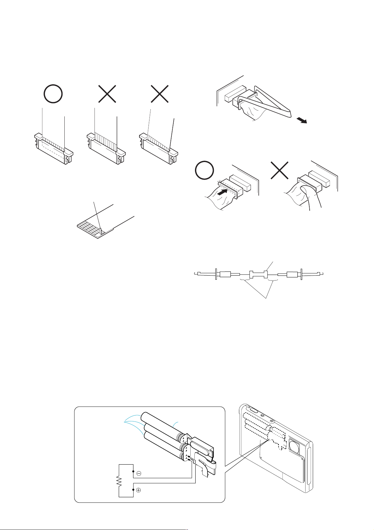
1. SERVICE NOTE
Make sure that the flat cable and flexible board are not cracked of
bent at the terminal.
Do not insert the cable insufficiently nor crookedly.
Cut and remove the part of gilt
which comes off at the point.
(Take care that there are
some pieces of gilt left inside)
When remove a connector, don't pull at wire of connector.
Be in danger of the snapping of a wire.
When installing a connector, don't press down at wire of connector.
Be in danger of the snapping of a wire.
[Discharging of the FLASH unit’s charging capacitor]
The charging capacitor of the FLASH unit is charged up to the
maximum 300 V potential.
There is a danger of electric shock by this high voltage when the
capacitor is handled by hand. The electric shock is caused by the
charged voltage which is kept without discharging when the main
power of the DSC-T7 is simply turned off. Therefore, the remaining
voltage must be discharged as described below.
Preparing the Short Jig
To preparing the short jig. a small clip is attached to each end of a
resistor of 1 kΩ /1 W (1-215-869-11)
Wrap insulating tape fully around the leads of the resistor to prevent
electrical shock.
Discharging the Capacitor
1 Remove the cabinet (front) assembly.
2 Peel off the absorbing sheet.
3 Remove the flexible board.
4 Short circuits between the positive and the negati ve terminals of
charged capacitor with the short jig about 10 seconds.
Capacitor
1 kΩ/1 W
Wrap insulating tape.
Flash unit
DSC-T7
Shorting jig
(1k
Ω
/ 1w)
1-1
Page 6

[Description on Self-diagnosis Display]
Self-diagnosis display
• C: ss: ss
The contents which can be handled
by customer, are displayed.
• E: ss: ss
The contents which can be handled
by engineer, are displayed.
Display Code
C:32:01
C:13:01
E:91:01
E:01:XX
E:61:00 *1
E:61:10 *1
Note : The error code is cleared if the battery is removed, except defective flash unit.
*1: The error display is given in two ways.
Turn off the main power then back on.
Replace the memory stick.
Format the memory stick with the DSC-T7.
Checking of flash unit or replacement of
flash unit.
Checking of lens drive circuit
Countermeasure
Trouble with hardware.
• The type of memory stick that cannot be
used by this machine, is inserted.
• Data is damaged.
• Unformatted memory stick is inserted.
Abnormality when flash is being
charged.
When failed in the focus initialization.
Cause
Caution Display During Error
SYSTEM ERROR
MS ERROR
Flash LED
Flash display
Flashing at 3.2 Hz
—
DSC-T7
1-2E
Page 7
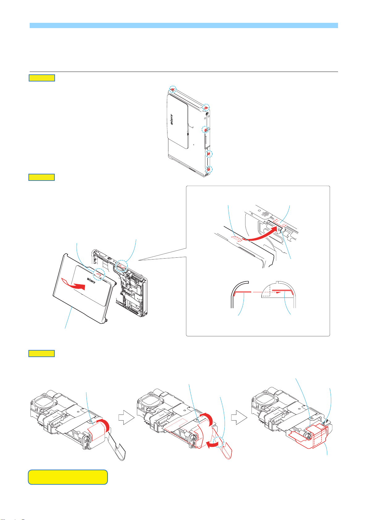
The following flow chart shows the disassembly procedure.
2-1. DISASSEMBLY
2. DISASSEMBLY
Some reassembling steps of the unit require attention.
Be sure to read HELP before reassembling.
4
a
e
5
b
Work while suppressing MC sheet metal
by the finger.
Note:
MC sheet metal.
2
MC sheet metal
3
1
2
3
4
5
1
SW-454 flexible board
Claw
SW-454 flexible board
T wo claws
Claw
SY-115
8
6
Flexible board
(from the Control switch block (RL51710))
7
Flexible board
(from the MS-258 board)
8
SY-115 board, MS guide assembly, etc.
Note:
Be careful not to deform
the Cabinet (front) assembly.
6
b
c
Be careful not to drop the
6
7
5
4
7
f
1
8
1
2
3
4
5
6
counterclockwise to disengage the claw e.
2
Two screws (M1.4x2.5) silver
Screw (M1.4x2.5) silver
Two screws (M1.4x2.5) silver
Twist the strap in the direction of arrow a.
Open the battery lid.
Grab b, c, and d, and apply force so that d turns
SY-115
7
Claw f
8
Cabinet (front) assembly
9
Ornamental plate
HELP 01
HELP 02
9
2
3
3
1
1
Absorbing sheet
2
Flexible board (from the LCD unit)
SY-115
4
1
Control switch block (GP51710)
2
Screw (M1.4x2.5) silver
3
Remove the two claws in the direction
of the arrow.
4
Main frame assembly, LCD unit, etc.
5
Cabinet (rear) assembly,
control switch block (GP51710), etc.
Be sure to discharge the capacitor.
SY-115
HELP 04
(disassembly of the control
switch block (GP51710))
1
2
Capacitors
5
Shorting jig
(1k
Ω
Caution
/ 1w)
Flash unit
4
7
5
1
Flexible board (Flash unit)
2
Pick up the AF guide
3
Two claws
4
Claw
5
T wo claws
6
AF LED
7
AF guide
8
Flash unit
SY-115
3
2
1
1
8
6
UKI sheet
2
Flexible board (from the lens unit)
3
Flexible board
(from the CCD block assembly)
4
Lens section
4
HELP 03
SY-115
1
3
2
DSC-T7
2
5
4
3
SY-115
1
Claw
2
MS guide assembly
3
SY insulating sheet
4
SW-454 flexible board
5
SY-115 board, battery terminal board
HELP 05
2
1
3
2
1
1
MS-258 board
2
Two MS electrostatic sheets
1
2
3
4
1
4
Control switch block (RL51710)
Claw
MC sheet metal
MC-149 board
HELP 06
(disassembly of the control
switch block (RL51710))
HELP 07
(disassembly of the piezo
speaker)
2-1 2-2
Page 8
2-2. SERVICE POSITION
b
4
6
5
2. DISASSEMBLY
2. DISASSEMBLY
a
c
[SERVICE POSITION TO CHECK THE SY-115 BOARD]
Note1: By using an adhesive tape, press the lens cover switch (S701).
7
SY-115
1
2
9
8
2
2
SY-115
1
SY-115
3
2
1
4
3
3
4
1
4
2
1
2
5
3
Note2: When checking the VIDEO AMP (SY-115 board IC350), connect an A/V connecting cable to the A/V jack of the conversion adaptor.
DC-IN
AC power
adaptor
AC IN
S701 Lens cover
switch (Note1)
Conversion
adaptor
CN001
LCD unit
Control switch block
(RL51710)
CN001
Control switch block
(GP51710)
Flash unit
MC-149 board
SY-115
1
CN002
4
7
5
8
6
SY-115
SY-115
1
3
2
SW-454
flexible board
CN706
SY-115 board,
Battery terminal board
1
2
3
SY-115
4
1
5
2
3
6
7
5
SY-115
8
4
CN707
BOARD
CN701
CN703
CN705
CN704
CN702
CD-541 board
MS-258 board
Lens section
Caution
Be sure to discharge the capacitor.
Flash unit
Capacitors
Shorting jig
(1kΩ / 1w)
DSC-T7
2-3 2-4
Page 9

2-3. CIRCUIT BOARDS LOCATION
MC-149
2. DISASSEMBLY
2. DISASSEMBLY
SY-115
NAME FUNCTION
CD-541
MC-149
SY-115
CCD IMAGER
MULTI CONNECTOR
LENS DRIVE, CAMERA A/D CONV., TIMING GENERATOR, CAMERA DSP, LENS CONTROL,
256M SDRAM, AUDIO PROCESS, CONNECTOR, DC/DC CONVERTER
CD-541
DSC-T7
2-5
Page 10
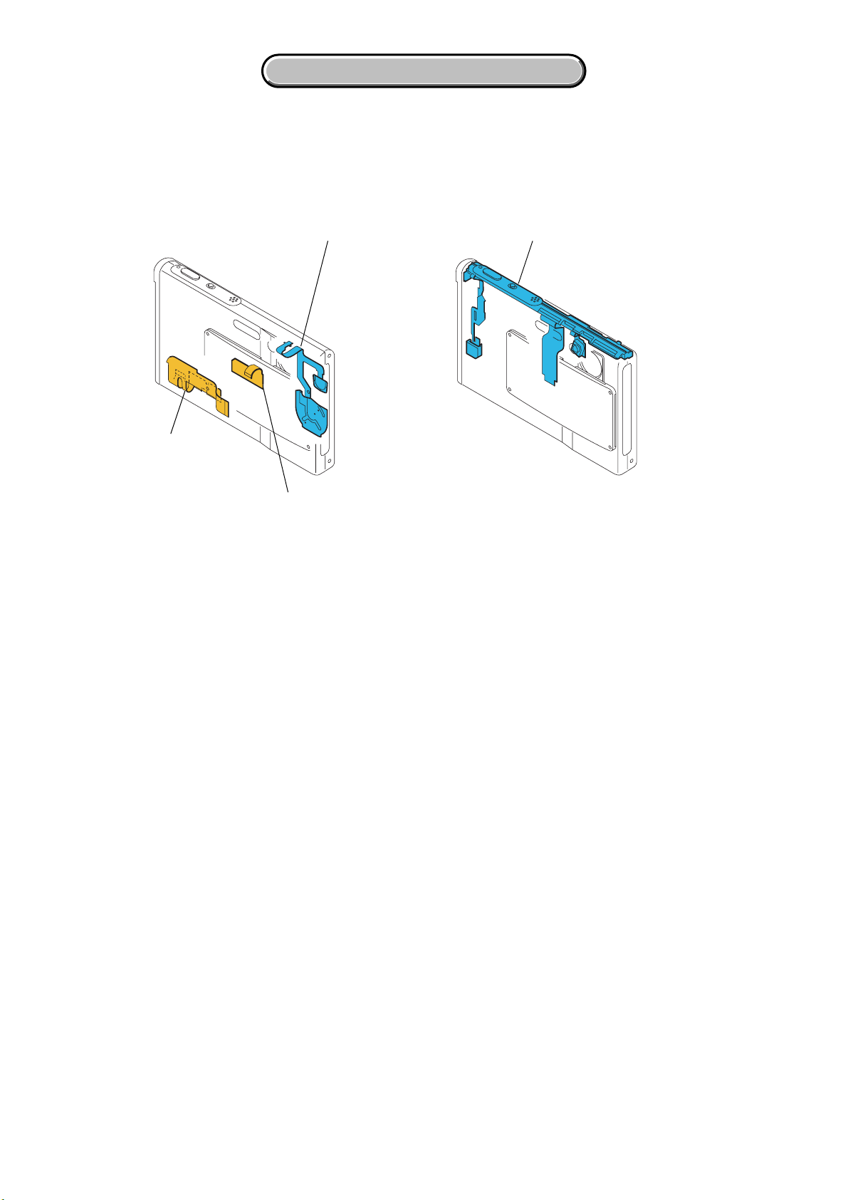
2-4. FLEXIBLE BOARDS LOCATION
The flexible boards contained in the lens block is not shown.
2. DISASSEMBLY
2. DISASSEMBLY
SW-454
CONTROL SWITCH BLOCK
(GP51710)
MS-258
CONTROL SWITCH BLOCK
(RL51710)
DSC-T7
2-6E
Page 11
HELP
Sheet attachment positions and procedures of processing the flexible boards/harnesses are shown.
HELP 01
To prevent the cabinet (front) assembly from
producing a gap, install the screws in the order
as in the figure on the right when reassembling.
HELP 02
When reassembling, insert the claw of the cabinet (front)
assembly under the claw of the cabinet (rear) assembly
at the deep end of the hole "a".
Claw of the Cabinet
Claw
(rear) assembly
1
2
3
4
5
Claw of the Cabinet
(front) assembly
Claw of the Cabinet
(rear) assembly
Cabinet (front) assembly
HELP 03
When reassembling, attach the CCD insulation sheet first, and then
attach the CD radiation sheet, adhesive surface of the CD-541 board.
CD radiation sheet
CCD insulation sheet
1
Claw of the Cabinet
(front) assembly
Adhesive surface of the
CD-541 board
2
Hole a
Claw of the Cabinet
(rear) assembly
CD radiation sheet
CCD insulation
sheet
Note:
Removing it CCD imager as a
single unit requires adjustment.
DSC-T7
3
CD-541 board
HELP
Page 12

HELP 04
(disassembly of the control
switch block (GP51710))
Control switch block (GP51710)
1
Insert a flat-tipped object such as a flat-head
screwdriver or tweezers into the gap on the control
switch block (GP51710). While slightly raising the
control switch block (GP51710), forcefully press the
two portions "a" in the direction of the arrow.
a
2
a
Control switch block (GP51710)
4
3
Insert a flat-tip object such as a flat-head screwdriver
or tweezers in the gap on the control switch block
(GP51710). While slightly raising the control switch
block (GP51710), forcefully press the two portions "b"
in the direction of the arrow.
b
b
DSC-T7
HELP
Page 13

HELP 05
When reassembling, attach MS electrostatic sheets in such a
way that they do not cover the four holes of the MS connector.
At that time, be sure to use new MS electrostatic sheets.
MS connector
Two MS electrostatic
sheets
Four holes
DSC-T7
HELP
Page 14

HELP 06
(disassembly of the control
switch block (RL51710))
3
ST capacitor
guide
2
ST cushion
1
Screw (M1.4x2.5) silver
4
Peel off the
piezo speaker
Piezo speaker
Main frame assembly
SP adhesive sheet
When removing the piezo speaker from the main frame assembly,
a part of the cushion of the piezo speaker is ripped apart, remaining
on the SP adhesive sheet on the main frame assembly.
When reassembling, remove the SP adhesive sheet and the cushion
of the piezo speaker left on the main frame assembly before using
a new SP adhesive sheet.
At this time, replace the piezo speaker also with a new one.
When reassembling, fit the three dowels of the main frame assembly
into the three positioning holes of the control switch block (RL51710).
DSC-T7
6
Control switch block
(RL51710), piezo speaker
5
Flexible board
(Block light guide plate)
Flexible board of the control
switch block (RL51710)
Three
positioning
holes
Main frame assembly
Three
dowels
HELP
Page 15

HELP 07
(disassembly of the
piezo speaker)
1
Remove soldering the two points
2
Control switch block (RL51710)
3
Piezo speaker
Positioning for soldering
Determine the position by aligning line "a" on the flexible board of
the control switch block (RL51710) with line "b" on the vibration
plate of the piezo speaker in parallel, and matching the positioning
hole on each of them.
Flexible board of the control
switch block (RL51710)
Positioning sheet for soldering
the piezo speaker
When soldering, print this sheet and use this as a
workbench for positioning.
cm
0
1
2
3
4
5
6
7
a
Positioning hole
b
Vibration plate
Piezo speaker
DSC-T7
8
9
10
Note: Use this drawing in its actual scale.
If you cannot print this out in its actual scale, the PC
or printer setting is a probable cause.
In such a case, use a photocopier or another tool to
obtain the actual size.
The solders must not run off the flexible board in the control switch
block (RL51710). At this time, the height of the solders must not
exceed 1 mm.
HELP
Page 16

Link
Link
3. BLOCK DIAGRAMS
POWER BLOCK DIAGRAMOVERALL BLOCK DIAGRAM
POWER BLOCK DIAGRAMOVERALL BLOCK DIAGRAM
DSC-T7
Page 17

3-1. O VERALL BLOCK DIAGRAM
3. BLOCK DIAGRAMS
Ver 1.1 2005. 06
( ) : Number in parenthesis ( ) indicates the division number of schematic diagram where the component is located.
LENS UNIT
(LSV-1040A)
BH001
BATTERY
TERMINAL
CN001 (1/2)
14
MULTI
CONNECTOR
13
12
MC-149
BOARD
(1/2)
SW-454
FLEIBLE(1/2)
CN002
CD-541 board is included in the CCD block assy.
CD-541 board is not supplied as an independent service parts.
1
H1A,B
H2A,B
RG
(1/7)
IRIS DRIVE
DRIVE
DRIVE
(7/7)
(7/7)
IC090
-7,5V/15V REG
15
XDD RST OUT
SAN0 SO
SAN0 SI
SAN0 SCK
BATT SENS
XPWR OFF
F5
E5
D3
F1
D5
A6
B6
C5
A2
C3
C4
A1
IC001
C5
C6
B6
G5
A7
B7
A4
BUFFER
EVER 3.1V
EVER 2.9V
D 3.1V
A 3.1V
MS VCC
CAM 2.9V
D 1.8V
M 5V
D 1.2V
BL H
BL L
XAF LED
CAM 15V
CAM -7.5V
IRIS A DIR
IRIS A BRK
IRIS B DIR
IRIS B BRK
FOCUS A DIR
FOCUS B DIR
FOCUS EN
ZOOM A DIR
ZOOM B DIR
ZOOM EN
FC SENS
ZM SENS
ST UNREG
SY-115 BOARD
EXTAL
D0-D31
A0-A12
(3/7)
IC352
42
35
C19,D18,B16
E19,A17,C18
C15,D17,B15
E18,C16,C17
B14,D16
C23
IC301
CAMERA DSP
SYSTEM CONTROL
B23
B17
E20
B18
Y22,U19,AB23,V20,AB22
W21,Y21,W22,AA22,AB21
AC22,AA21,Y20,AA20,V19
W20,J22,H20,K20,H19
L21,J20,K21,J19,K22,K19
M22,L19,L20,M20,L22,M19,
P20,T22,R21,U22
P19,R19,R20,U21
T19,V21,T21,V22,T20
C14
C13
E13
D13
A13
E15
D15
A12
D14
B12
B10
E10
TXD4
W6
AC6
RXD4
AB9
XACV IN
D7
SAN0 SO
D8
SAN0 SI
C5
SAN0 SCK
AA16
BATT SENS
Y10
XDD RST OUT
B7
AC7
XPWR OFF
AC19
V OUT
SAN1 SO, SCK
D3,E2,F3
D2,E3,E1
(3/7)
D21
G19,J23,F19
F20,G21,G22
F22,H22
H21
G20
H23
D11
SAN1 SO, SI, SCK
B11
D12
E9
G5
Y17
W11
AC9
W4
E12
AA13
AB13
Y12
W15
AB14
Y19
AB20
MS D0-MS D3, MS BS, MS CLK
XACCESS LED
F3
SAN1 SO, SCK
E3
D701
(MS ACCESS)
STRB CHG
XSTRB FULL
STRB CHG CONT
STRB ON
KEY AD0
XAE LOCK SW
XSHUTTER SW
KEY AD1
MODE DIAL 0
XPWR LED
XSTRB LED
(5/7)
LCD D0-D7
LCD HD
LCD VD
LCD CK
SAN1 SO, SCK
XSAN RST OUT
LCD ADJ 1
3,2,4,6,1,7
CN704
CN707
ST UNREG
CN705
IC602
SAN_AUIN
AC17
SAN_AUOUT
AC15
A5
USB D+,D-
A4
Q304
C10
AA9
USB VBUS
XAV JACK IN
MIC AMP
E6
C1
SPEAKER AMP
B1
E5
AU OUT AMP
4
IC603
SPEAKER AMP
B6
A5
A2
D1
C2
(5/7)
3
CN703
CN706
(1/2)
97,98,100,101
103,104,105,3
CAMERA
3
15
CCD OUT
60
IC101
37
2
3
5
6
13
CN701
(2/2)
40
44
48
53
11,8
16,12
9,91
5,6
88,102
90, 72
SAN0 SO, SI, SCK
GENERATOR
A/D CONV.
(2/7)
TIMING
89 93
SAN1 SO,SCK
2,4,7,10,14,18
56
77
80
V LINE OUT
CA AD0 - CA AD13
CLK TGO
CA HD
CA FD
(4/7)
IC403
256Mbit
SDRAM
BATT SIG
X302
12MHz
XTAL OSC
IRIS A DIR
IRIS A BRK
IRIS B DIR
IRIS B BRK
FOCUS A DIR
FOCUS B DIR
FOCUS EN
ZOOM A DIR
ZOOM B DIR
ZOOM EN
FC SENS
ZM SENS
Q302
I/F
(3/7)
IC350
VIDEO AMP
MS-258 BOARD
5
21
28
30
31
29
COLOR LCD
33
32
35
15
FLASH UNIT
8
4
6
6
10
5
7
4
8
9
6
3
9
4
2
10
16
S002
11
SHUTTER
4
AE LOCK
6
S005
20
23
PLAY,STILL,MOVIE
3
9
XAF LED
25
VL 3V
1
XPWR ON
14
BL H
18
BL L
19
7
13
12
KEY AD1
21
21
2
2
3
3
5
5
SW-454
FLEXIBLE
(2/2)
7
7
8
8
10
10
CN001
MS D0-MS D3, MS BS, MS CLK
XMS IN
LCD901
2.5 INCH
PANEL
7
T001
Q001
IGBT
IC002
FLASH DRIVE
S003,004
CHG
XFULL
I_PEAK
G_IGBT
F_ON
TELE, WIDE
CONTROL SWITCH
BLOCK(RL51710)
D001 (POWER)
D002 (FLASH)
D003 (AF LED)
S001
POWER
S001,002
DUST, DISPLAY
20
19
17
15
14
12
CN002
4,3,5,7,2,8
LED901
LCD
BACK
LIGHT
BT001
LITHIUM
BATTERY
(SECONDARY)
MIC SIG
SP+
SP-
20
19
17
MC-149
BOARD(2/2)
15
14
12
CN002
6
CN004
CN002
3
4
2
1
6
5
USB D+,D-
USB VBUS
XAV JACK IN
AU LINE OUT
V LINE OUT
CN101
MEMORY
STICK
DUO
CONNECTOR
XENON
TUBE
S004,002,003,001.006
LEFT, RIGHT, UP, DOWN, SET
S005
MENU
CN001
MIC901
MIC
SP901
SPEAKER
10
9
7
6
3
5
CONTROL
SWITCH
BLOCK
(GP51710)
CN001(2/2)
MULTI
CONNECTOR
S701
LENS BARRIER
OPEN
18
21
1
4
5
8
14
11
CN702
32.768KHz
CD-541 BOARD
IC002
CCD IMAGER
1-5
27,26
7-14
20-32
F2
E2
D2
B1
D6
E6
B7
C6
B4
B5
B3
A3
A8
OSC I
A9
OSC O
B8
VL 3V
C7
XPWR ON
C9
USB VBUS
B10
XMS IN
XLENS B OPEN
D7
19-17
CN701(1/2)
IRIS A
IRIS A
IRIS B
IRIS B
FOCUS A
FOCUS A
FOCUS B
FOCUS B
ZOOM A
ZOOM A
ZOOM B
ZOOM B
F001
F002
X001
V1A,B
V2
V3A,B
V4
V5A,B
V6
V7A,B
V8
VHLD
UNREG
IC201
FOCUS MOTOR
ZOOM MOTOR
IC001
DC/DC CONVERTER
REAL TIME CLOCK
IRIS
SHUTER
IRIS
MOTOR
M
FOCUS
MOTOR
M
ZOOM
MOTOR
M
FOCUS RESET
SENSOR
ZOOM RESET
SENSOR
13
16
6
|
6
13
|
16
CN706(2/2)
Q001,002
D004
BATT/XEXT
ACV UNREG
()
BATT UNREG
BATT SIG
C
BATT GND
CN002
16
16
9
9
|
|
6
6
CN001
DSC-T7
3-1 3-2
Page 18

3-2. POWER BLOCK DIAGRAM
Ver 1.1 2005. 06
( ) : Number in parenthesis ( ) indicates the division number of schematic diagram where the component is located.
CONTROL
SWITCH
BLOCK
(GP51710)
D_3.1V
BH001
BATTERY
TERMINAL
CN001
14
MULTI
CONNECTOR
13
12
MC-149 BOARD
SW-454 FLEIBLE
BT001
LITHIUM
BATTERY
(SECONDARY)
CONTROL SWITCH
BLOCK(RL51710)
D001 (POWER)
D002 (FLASH)
1
19
CN004
D003 (AF LED)
S001
POWER
LED901
LCD
BACK
LIGHT
COLOR LCD
CN002
LCD901
2.5 INCH
PANEL
VL 3V
SY-115 BOARD
BATT UNREG
BATT SIG
C
BATT GND
CN002
16
2
1
6
5
9
|
6
16
9
|
6
D 3.1V
M 5V
XAF LED
XPWR ON
BL H
BL L
CN002
CN001
6
13
|
16
13
16
1
3
9
10
17
24
25
14
18
19
17
6
|
BATT/XEXT
ACV UNREG
CN706
CN703
D 3.1V
CN707
Q001,002
D004
BATT SIG
F001
Q302
I/F
STRB CHG
XSTRB FULL
STRB CHG CONT
XACV IN
(3/7)
IC352
4
5
-7.5V ON
D 1.8V
2
D 3.1V
A 3.1V
AU 3.1V
D 1.8V
D 1.2V
F002
W11
AC9
W4
AB9
W6
AC6
AB11
Y19
AB20
R010
TXD4
RXD4
XPWR LED
XSTRB LED
L401
(3/7)
IC301
CAMERA DSP
SYSTEM CONTROL
SDRAM VCC
IC403
D005
EVER 2.9V
EVER 3.1V
XCS DD
SAN0 SO
SAN0 SI
XSAN0 SCK
LENS BARRIER
()
(4/7)
256Mbit
SDRAM
S701
OPEN
FLASH UNIT
D302
D 3.1V
D 3.1V
M 5V
AU 3.1V
T001
IC002
XE DRIVE
(3/7)
IC350
VIDEO AMP
(2/7)
IC101
S/H
A/D CONV.
TIMING GENERATOR
L101
(1/7)
IC201
IRIS DRIVE
FOCUS MOTOR DRIVE
ZOOM MOTOR DRIVE
(5/7)
IC602
MIC AMP
SPEAKER AMP
AU OUT AMP
XENON
D 3.1V
CAM 15V CD
R704
MS-258
BOARD
8
CN704
CD-541 BOARD
17
10
CN701
CD-541 board is included in the CCD block assy.
CD-541 board is not supplied as an independent
service parts.
LENS UNIT
(LSV-1040A)
FC SENS VCC
15
R703
ZM SENS VCC
12
CN702
MS VCC
IC001
IC002
BUFFER
CCD IMAGER
FOCUS
RESET
SENSOR
ZOOM
RESET
SENSOR
CN101
MEMORY
9
STICK
DUO
CONNECTOR
L001
8
ST UNREG
UNREG
(7/7)
A1
2.9V REG
1.8V REG
PWR1-1
PWR1-2
PWR1-3
VO1-1
VO1-2
MS PWR IN
MS PWR
LDO3IN
LDO3
LDO2IN
LDO2
UNREG2
PWR56 OUT
LX5-1
LX5-2
LX5-3
LX5-4
PSG4
B1
C2
F1
F2
H2VFB1
L009
G1
G2
B2
A2
B3
A3
J6
K6
J7
K7
L007
J9
J10
K9
K10
H9VFB5
D10PWR2
C10LX2
D8VFB2
E10LX3
E9VO3
LV3
F9
RS3
F8
G9BG4
F10
TG4
F7VFB4
G8
L002
Q003
SWITCHING
D092
(RECT)
D007
(RECT)
C091
D006
(RECT)
D090,091
(RECT)
L005
L006
Q004
RECT
BL H
BL L
SWITCH
Q005
(7/7)
15V REG
IC090
-7.5V REG
3
1
-7.5V ON
IC001
DC/DC CONVERTER
REAL TIME CLOCK
J1
UNREG1-1,2
K1
LDO1
H1
3.1V REG
VL 3V
B8
RTC BAT
A8
XPWR ON
A9
G5
A7
B7
D3
A6
C5
C6
B6
A4
C7
D7
OSC I
OSC O
UNREGMON
XRESET
XPWR OFF
MS PWR ON
XCS DD
SAN0 SO
SAN0 SI
XSAN0 SCK
XAF LED
XPWRON1
XPWRON2
X001
32.768KHz
BATT SENS
AA16
XDD RST OUT
Y10
B7
XPWR OFF
AC7
MS PWR ON
Y11
Y9
D7
D8
C5
XLENS B OPEN
ST UNREG
STRB CHG
XSTRB FULL
STRB CHG CONT
67
4
(5/7)
IC603
SPEAKER AMP
(5/7)
IC604
A1
C3
3.1V REG
4
|
|
6
6
5
7
4
8
3
9
M_5V
1
11
CN705
D 3.1V
L003
A 3.1V
MS VCC
CAM 2.9V
D 1.8V
CAM 15V
CAM -7.5V CAM -7.5V CD
D 1.2V
M 5V
C1
AU 3.1V
CHG
10
XFULL
9
6
I_PEAK
3
VCC
DSC-T7
-7.5V ON
BL H, BL L
M 5V
D 3.1V
A 3.1V, D 1.8V, D 1.2V, AU 3.1V
3-3 3-4E
Page 19

4-1. FRAME SCHEMATIC DIAGRAM
1
3 18
A
6PCN002
1
BL_H
65432
N.C
N.C
BL_L
BL_L
BL_H
B
C
MEMORY STICK
DUO
CONNECTOR
D
E
F
G
LCD BACK LIGHT
H
2.5INCH LCD PANEL
I
J
K
4
I
G
BATTERY
TERMINAL
CN101
REG_GND
MS_VCC
MS_CLK
DATA3
DATA2
DATA0
DATA1
REG_GND
10P
10
9
8
7
INT
6
5
4
3
2
BS
1
1 BATT_UNREG
2 BATT_SIG
3 BATT_GND
CN707
39
VCOM
38
TFT-COM
37
N.C.
36
VSS
35
XRESET
34
XCS
33
SI
32
SCLK
31
VSYNC
30
HSYNC
29
DCK
28
D7
27
D6
26
D5
25
D4
24
D3
23
D2
22
D1
21
D0
20
N.C.
19
VS
18
COMDC
17
VDD
16
VR
15
VCOMH
14
N.C.
13
VGH
12
VGL
11
C2+
10
C2-
9
C3+
8
C3-
7
COMC
6
VDD2
5
C1+
4
C1-
3
VSS
2
TFT-COM
1
VCOM
6 14 17
MS-258 BOARD
MS I/O CONNECTOR
123456789
MS_D1
MS_D0
MS_BS
39P
4. PRINTED WIRING BOARDS AND SCHEMATIC DIAGRAMS
25
XAF_LED
8
CONTROL SWITCH BLOCK
(RL51710)
BL_L
REG_GND
REG_GND
BL_H
KEY_AD1_L2
D_3.1V
123456789
REG_GND(USB)
M_5V
MODE_DIAL0
92 10
SP-
SP+
KEY_AD0
REG_GND
XPWR_ON
25PCN703
USB_D-
USB_D+
USB_VBUS
BATT/XEXT
REG_GND(USB)
101112131415161718192021222324
D_3.1V
MIC_SIG
MIC_GND
REG_GND
XSTRB_LED
XAE_LOCK_SW
XAV_JACK_IN
KEY_AD1_L3
21PCN706
B TO B
1011121314151617181920
REG_GND
REG_GND
ACV_UNREG
V_LINE_OUT
AU_LINE_OUT
REG_GND(AV)
CN001 21P B TO B
XPWR_LED
XSHUTTER_SW
ACV_UNREG
ACV_UNREG
123456789
VL_3V
REG_GND
REG_GND
ACV_UNREG
REG_GND
REG_GND
11 12
FLASH UNIT
FLASH DRIVE
10
11
REG_GND
REG_GND
REG_GND
REG_GND
21
KEY_AD1
ST_UNREG
ST_UNREG
ST_UNREG
11PCN705
XSTRB_FULL
STB_CHARGE
I_PEAK
STRB_ON
123456789
M_5V
MS_D2
7
10
11
MS_D3
XMS_IN
MS_CLK
MS_VCC
REG_GND
REG_GND
REG_GND
11PCN704
SY-115 BOARD
(1/7) LENS DRIVE
(2/7) CAMERA A/D CONV.TIMING GENERATOR
(3/7) CAMERA DSP,LENS CONTROL
(4/7) 256M SDRAM
(5/7) AUDIO PROCESS
(6/7) CONNECTOR
(7/7) DC/DC CONVERTER
135
REG_GND
1
H1A
2
H2A
3
REG_GND
4
H1B
5
H2B
6
REG_GND
7
CSUB
8
SHT
9
CAM_-7.5V_CD
10
POWER_SAVE
11
REG_GND
12
RG
13
REG_GND
14
15
CCD_OUT
33PCN701
16
REG_GND
17
CAM_15V_CD
18
REG_GND
19
VST
20
V3B
21
V3A
22
V1A
23
V1B
24
V2
25
V7B
26
V8
27
V7A
28
V6
29
VHLD
30
V5B
31
V5A
32
V4
33
REG_GND
1 FOCUS_A
2
FOCUS_B
3 FOCUS_A
4 FOCUS_B
5 ZOOM_B
6 ZOOM_A
ZOOM_B
7
ZOOM_A
8
21P
9 TEMP_GND
10 LENS_TEMP
CN702
11 ZM_SENS
12 ZM_SENS_VCC
13 ZM_SENS_GND
14 FC_SENS
15 FC_SENS_VCC
16 FC_SENS_GND
17 N.C.
IRIS_A
18
19 IRIS_A
IRIS_B
20
21 IRIS_B
15
CN004
6P
6
REG_GND
12345
N.C.
N.C.
D_3.1V
UP(KEYAD1-2)
RIGHT(KEYAD1-1)
CONTROL SWITCH BLOCK
(GP51710)
CD-541 BOARD
CCD IMAGER
16
Ver 1.1 2005. 06
19
CCD IMAGER
LENS UNIT
L
M
N
DSC-T7
SW-454 FLEXIBLE BOARD
SW,SY-MC RELAY
CN002 21P B TO B
AU_LINE_OUT
REG_GND(AV)
REG_GND
V_LINE_OUT
21PCN002
1011121314151617181920
REG_GND
ACV_UNREG
ACV_UNREG
B TO B
ACV_UNREG
ACV_UNREG
BATT/XEXT
14
ACV_UNREG
13
ACV_UNREG
12
11
1
8
MULTI
CONNECTOR
7
14
15 16
16
USB_GND
USB_D+
USB_D-
USB_GND
USB_VBUS
XAV_JACK_IN
V_LINE_OUT
RED_GND
AU_LINE_OUT
ACV_GND
ACV_GND
10
9
14PCN001
8
7
6
5
4
3
2
1
MC-149 BOARD
MULTI CONNECTOR
21
USB_D+
REG_GND(USB)
USB_D-
REG_GND(USB)
USB_VBUS
BATT/XEXT
XAV_JACK_IN
4-1
REG_GND
REG_GND
REG_GND
REG_GND
123456789
REG_GND
4-2
FRAME SCHEMATIC DIAGRAM
Page 20

Link
Link
4-2. SCHEMATIC DIAGRAMS
CD-541 BOARD
CD-541 BOARD
MC-149 BOARD
MC-149 BOARD
MS-258 BOARD
MS-258 BOARD
SW-454 FLEXIBLE BOARD
SW-454 FLEXIBLE BOARD
(SW, SY-MC RELAY)
(SW, SY-MC RELAY)
COMMON NOTE FOR SCHEMATIC DIAGRAMS
COMMON NOTE FOR SCHEMATIC DIAGRAMS
(CCD IMAGER)
(CCD IMAGER)
(MULTI CONNECTOR)
(MULTI CONNECTOR)
(MS I/O CONNECTOR)
(MS I/O CONNECTOR)
CONTROL SWITCH BLOCK
CONTROL SWITCH BLOCK
CONTROL SWITCH BLOCK
CONTROL SWITCH BLOCK
FLASH UNIT
FLASH UNIT
(FLASH DRIVE)
(FLASH DRIVE)
WAVEFORMS
WAVEFORMS
(GP51710)
(GP51710)
(RL51710)
(RL51710)
DSC-T7
Page 21

4-2. SCHEMATIC DIAGRAMS
l
4-2. SCHEMATIC DIAGRAMS
THIS NOTE IS COMMON FOR SCHEMATIC DIAGRAMS
(In addition to this, the necessary note is printed in each block)
Ver 1.1 2005. 06
(For schematic diagrams)
• All capacitors are in µF unless otherwise noted. pF : µ
Link
µF. 50 V or less are not indicated except f or electrolytics
and tantalums.
• Chip resistors are 1/10 W unless otherwise noted.
kΩ=1000 Ω, MΩ=1000 kΩ.
• Caution when replacing chip parts.
New parts must be attached after removal of chip.
Be careful not to heat the minus side of tantalum
capacitor, Because it is damaged by the heat.
• Some chip part will be indicated as follows.
Example C541 L452
22U 10UH
TA A 2520
Kinds of capacitor
Temperature characteristics
External dimensions (mm)
• Constants of resistors, capacitors, ICs and etc with XX
indicate that they are not used.
In such cases, the unused circuits may be indicated.
• Parts with * differ according to the model/destination.
Refer to the mount table for each function.
• All variable and adjustable resistors have characteristic
curve B, unless otherwise noted.
• Signal name
XEDIT→ EDIT PB/XREC → PB/REC
• 2: non flammable resistor
• 5: fusible resistor
• C: panel designation
• A : B+ Line
• B : B– Line
• J : IN/OUT direction of (+,–) B LINE.
• C: adjustment for repair.
• A : VIDEO SIGNAL (ANALOG)
• A : AUDIO SIGNAL (ANALOG)
• A : VIDEO/AUDIO SIGNAL (ANALOG)
• A : VIDEO/AUDIO/SER V O SIGNAL
• A : SERVO SIGNAL
• Circled numbers refer to waveforms.
(Measuring conditions voltage and waveform)
• Voltages and waveforms are measured between the
measurement points and ground when camera shoots
color bar chart of pattern box. They are reference v alues
and reference waveforms.
(VOM of DC 10 MΩ input impedance is used)
• Voltage values change depending upon input
impedance of VOM used.)
1. Connection
Pattern box Color bar chart
Pattern box PTB-450
J-6082-200-A
or
Small pattern box
PTB-1450
J-6082-557-A
Pattern box
Conversion adpter
1-819-219-11: Except US mode
1-819-219-31:US model
About 28 cm (PTB-450)
About 12 cm (PTB-1450)
Front of the lens
Stand assembly
X-2055-343-1
2. Adjust the distance so that the output waveform of
Fig. a and the Fig. b can be obtain.
H
Yellow
Cyan
White
Magenta
Green
AABBA=B
Fig. a (Video output terminal output waveform)
Red
Blue
Electronic beam
scanning frame
CRT picture frame
For PTB-450:
J-6020-250-A
For PTB-1450:
J-6082-559-A
Precautions Upon Replacing CCD imager
• The CD-541 board mounted as a repair part is not equipped
with a CCD imager.
When replacing this board, remove the CCD imager from
the old one and mount it onto the new one.
• If the CCD imager has been replaced, carry out all the
adjustments for the camera section.
• As the CCD imager may be damaged by static electricity
from its structure, handle it carefully like for the MOS IC.
In addition, ensure that the receiver is not covered with
dusts nor exposed to strong light.
DSC-T7
Fig.b (Picture on monitor TV)
When indicating parts by reference number, please
include the board name.
Note :
The components identified by
mark 0 or dotted line with mark
0 are critical for safety.
Replace only with part number
specified.
Note :
Les composants identifiés par
une marque 0 sont critiques
pour la sécurité.
Ne les remplacer que par une
pièce portant le numéro spécifié.
4-3
Page 22

4-2. SCHEMATIC DIAGRAMS
For Schematic Diagram
• Refer to page 4-29 for printed wiring board.
A
B
C
D
E
F
1
CD-541 BOARD
CCD IMAGER
XX MARK:NO MOUNT
TO
SY-115 BOARD(2/7)
CN701
(PAGE 4-15
OF LEVEL3)
NO MARK:REC/PB MODE
R :REC MODE
P :PB MODE
:Voltage measurement of
the CSP IC and
the Transistors with
mark,is not possible.
33P
H1A
H2A
H1B
H2B
SHT
VST
V3B
V3A
V1A
V1B
V7B
V7A
V5B
V5A
RG
1
2
3
4
5
6
7
8
9
10
11
12
13
14
15
16
17
18
19
20
21
22
23
24
V2
25
26
V8
27
28
V6
29
30
31
32
V4
33
REG_GND
REG_GND
REG_GND
CSUB
CAM_-7.5V_CD
POWER_SAVE
REG_GND
REG_GND
CCD_OUT
REG_GND
CAM_15V_CD
REG_GND
VHLD
REG_GND
LND001
LND002
LND003
LND004
LND005
LND006
LND007
LND008
LND009
LND010
LND011
LND012
LND013
LND014
LND015
LND016
LND017
LND018
LND019
LND020
LND021
LND022
LND023
LND024
LND025
LND026
LND027
LND028
LND029
LND030
LND031
LND032
LND033
VST
V3B
V3A
V1A
V1B
V7B
V7A
VHLD
V5B
V5A
CD-541 board is included in the CCD block assy
and it is not supplied as an independent service parts.
H1A
H2A
H1B
H2B
CSUB
SHT
RG
IC001
CXA3691EN-T9
R11.4
P0
1
IN
R15.1/P0
2
R11.4
P0.1
V2
V8
R006
0
1
GND
OUT
IDRV
3
ISF
VCC
6
5
4
IC001
V6
V4
BUFFER
R4.1
P0
C001
0.01u
B
R003
220k
6352
V1A
V1B
V2
V3A
V3B
VST
V4
V5A
V5B
VHLD
V6
11
10
V6
VHLD
XX
C002
V7A
V7B
V8
C003
0.1u
16V
B
RG
H1B
H2B
SHT
CSUB
H1A
H2A
12
13
14
15
16
17
V7A
V7B
V8
CCD-OUT
VH
RG
R2.9
P0
18
R004
1500
1
2
3
Q002
DTC144EMT2L
SWITCH
CSP(CHIP SIZE PACKAGE)IC
H1B19H2B20RSS321GND
R0.1
P0
8
7V48
9
V5A
V5B
IC002
CCD IMAGER
IC002
ICX495CQZ-13
WGND23SUB24CSUB
22
1200
R005
4
5
6
V3A
V3B
VST
VL
25
C005
0.1u
16V
V1B
V1A
H2A
H1A
B
947
V2
3
2
1
27
26
C004
0.1u
B
16V
DSC-T7
16
4-5
4-6
CD-541
Page 23

For Schematic Diagram
• Refer to page 4-29 for printed wiring board.
A
B
C
D
1
MC-149 BOARD
MULTI CONNECTOR
XX MARK:NO MOUNT
TO
SW-454 FLEXIBLE BOARD
CN002
(PAGE 4-8)
16
256
21P
CN002
REG_GND(USB)
REG_GND(USB)
USB_VBUS
BATT/XEXT
XAV_JACK_IN
AU_LINE_OUT
REG_GND(AV)
V_LINE_OUT
REG_GND
REG_GND
ACV_UNREG
ACV_UNREG
ACV_UNREG
ACV_UNREG
REG_GND
REG_GND
REG_GND
REG_GND
REG_GND
USB_D+
USB_D-
21
20
19
18
17
16
15
14
13
12
11
10
9
8
7
6
5
4
3
2
1
LND101
43
CN001
14P
1
ACV_GND
2
ACV_GND
3
AU_LINE_OUT
4
RED_GND
5
V_LINE_OUT
6
XAV_JACK_IN
7
USB_VBUS
8
USB_GND
9
USB_D-
10
USB_D+
11
USB_GND
12
ACV_UNREG
13
ACV_UNREG
14
BATT/XEXT
CN001 and CN002 are included
1516
7
MULTI
CONNECTOR
814
1
A
B
1
SW-454 FLEXIBLE BOARD
SW,SY-MC RELAY
XX MARK:NO MOUNT
TO
SY-115 BOARD(6/7)
CN706
(PAGE 4-23 OF LEVEL3)
in this complete of MC-149 board.
there are not supplied separately.
C
D
3
4
R002
2200
S001
4
CN002
21P
REG_GND(USB)
21
USB_D+
20
USB_D-
19
REG_GND(USB)
18
USB_VBUS
17
BATT/XEXT
16
XAV_JACK_IN
15
AU_LINE_OUT
14
REG_GND(AV)
13
12
11
10
9
8
7
6
5
4
3
2
1
V_LINE_OUT
REG_GND
REG_GND
ACV_UNREG
ACV_UNREG
ACV_UNREG
ACV_UNREG
REG_GND
REG_GND
REG_GND
REG_GND
REG_GND
1
2
S002
3
DISPDUST
LEVEL2LEVEL1
4
TO
MC-149 BOARD
CN002
(PAGE 4-7)
2
CN001
REG_GND(USB)
REG_GND(USB)
XAV_JACK_IN
AU_LINE_OUT
REG_GND(AV)
V_LINE_OUT
ACV_UNREG
ACV_UNREG
ACV_UNREG
ACV_UNREG
35
21P
B TO B B TO B
1
USB_D+
USB_D-
USB_VBUS
BATT/XEXT
REG_GND
REG_GND
REG_GND
REG_GND
REG_GND
REG_GND
KEY_AD1
2
3
4
5
6
7
8
9
10
11
12
13
14
15
16
17
18
19
20
21
1
2
For Schematic Diagram
• Refer to page 4-30 for printed wiring board.
1
2
MS-258 BOARD
MS I/O CONNECTOR
A
B
XX MARK:NO MOUNT
TO
SY-115 BOARD(6/7)
CN704
(PAGE 4-24
OF LEVEL3)
16
MS_BS
MS_D1
MS_D0
MS_D2
XMS_IN
MS_D3
MS_CLK
MS_VCC
REG_GND
REG_GND
REG_GND
11P
16
453
CN101 is included in this complete of MS-258 board.
It is not supplied separately.
10P
CN101
REG_GND
1
1
2
3
4
5
6
7
8
9
10
11
BS
2
DATA1
3
DATA0
4
5
DATA2
6
INT
7
DATA3
MS_CLK
8
MS_VCC
9
REG_GND
10
MEMORY STICK
DUO
CONNECTOR
DSC-T7
4-7 4-8
MC-149/MS-258/SW-454
Page 24

For Schematic Diagram
• Refer to page 4-29 for printed wiring board.
Ver 1.1 2005. 06
A
B
C
D
E
1
TO
SY-115 BOARD(6/7)
CN703
(PAGE 4-23 OF LEVEL3)
28
65
79
1034
CONTROL SWITCH BLOCK
(RL51710)
FUNCTION KEY
XSHUTTER_SW
XAE_LOCK_SW
SP901
SPEAKER
VL_3V
REG_GND
XPWR_LED
REG_GND
KEY_AD1_L3
MIC_SIG
MIC_GND
XSTRB_LED
D_3.1V
XPWR_ON
REG_GND
KEY_AD0
D_3.1V
BL_H
BL_L
KEY_AD1_L2
REG_GND
REG_GND
MODE_DIAL0
M_5V
XAF_LED
SP-
SP+
25P
1
2
3
4
5
6
7
8
9
10
11
12
13
14
15
16
17
18
19
20
21
22
23
24
25
(AUTO FOCUS)
R006
SML-412MWT86
POWER LED(GREEN)
STRB_LED(YELLOW)
D003
S4G49
33
D001
D002
SML-512WWT86
BT001
LITHIUM BATTERY
(SECONDARY)
R002
10k
S004
T
S002
S001
ZOOM
1
2
3
4
5
6
1
2
3
4
5
6
CN002
BL_H
BL_H
N.C.
N.C.
BL_L
BL_L
D_3.1V
N.C.
KEY_AD00
KEY_AD1_L2
N.C.
REG_GND
6P
6PCN004
BACK LIGHT UNIT
LED901
BACK LIGHT
6P
CN001
N.C.
N.C.
1
2
3
4
5
6
D_3.1V
KEY_AD00
KEY_AD1_L2
REG_GND
R006
10k
R001
2200
R002
2200
R003
4700
R005
10k
S003
W
3
4
1
SHUTTER
AE LOCK
2
POWER
F
DSC-T7
16
MIC901
Note :
The components identified by
mark 0 or dotted line with mark
0 are critical for safety.
Replace only with part number
specified.
4-9 4-10
Note :
Les composants identifiés par
une marque 0 sont critiques
pour la sécurité.
Ne les remplacer que par une
pièce portant le numéro spécifié.
R003
2200
R004
2200
R005
2200
S005
PLAY
STILL
MOVIE
S005
MENU DOWN RIGHT UP LEFT SET
S001 S002
S003
S004
CONTROL SWITCH BLOCK
(GP51710)
FUNCTION KEY
CONTROL SWITCH BLOCK (GP51710) is replaced as a block.
So that this PRINTED WIRING BOARD is omitted.
S006
GP51710/RL51710
Page 25

1
283
5
74
1069
A
B
C
D
FLASH UNIT
FLASH DRIVE
XX MARK:NO MOUNT
TO
SY-115 BOARD(6/7)
CN705
(PAGE 4-24 OF LEVEL3)
FLASH UNIT is replaced as a block.
So that this PRINTED WIRING BOARD is omitted.
11P
L001
2.2uH
C002
22u
C
6.3V
17
LND011
1REG_GND
LND010
2REG_GND
LND009
3REG_GND
LND008
4ST_UNREG
LND007
5ST_UNREG
LND006
6ST_UNREG
LND005
7STB_CHARGE
LND004
8XSTB_FULL
LND003
9I_PEAK
LND002
10STRB_ON
LND001
11M_5V
C001
1u
B
1
SW
2
SW
3
VCC
4
F_ON
HGND
TPS65552RGTR
N.C.6I_PEAK7G_IGBT8N.C.
5
T001
2
1
4
3
15
16
N.C.
IC002
FLASH DRIVE
IC002
6
5
14
13
N.C.
N.C.
VBATT
PGND
PGND
XFULL
CHG
12
11
10
9
D001
FT02P80TP
LND012
LND003
MC+
MC-
LND014
LND005
MC+
MC-
LND016
LND007
MC+
MC-
R003
1M
0.047u
C006
LND018
TRIGGER
LND019
TRIGGER_GND
CY25BAJ-BF-T23
LND020
XE_H
LND021
XE_L
Q001
IGBT
TRIGGER
COIL
XENON
TUBE
R001
33
R002
1M
E
16
Note :
The components identified by
mark 0 or dotted line with mark
0 are critical for safety.
Replace only with part number
specified.
Note :
Les composants identifiés par
une marque 0 sont critiques
pour la sécurité.
Ne les remplacer que par une
pièce portant le numéro spécifié.
Schematic diagram of the SY-115 board are not shown.
Pages from 4-13 to 4-26 are not shown.
DSC-T7
4-11 4-12
FLASH UNIT
Page 26

Link
Link
4-3. PRINTED WIRING BOARDS
CD-541 FLEXIBLE BOARD
CD-541 FLEXIBLE BOARD
CONTROL SWITCH BLOCK (RL51710)
CONTROL SWITCH BLOCK (RL51710)
MC-149 BOARD
MC-149 BOARD
CIRCUIT BOARDS LOCATION
CIRCUIT BOARDS LOCATION
NAME FUNCTION
CD-541
MC-149
MS-258
SY-115
SW-454
CCD IMAGER
MULTI CONNECTOR
MS I/O CONNECTOR
LENS DRIVE, CAMERA A/D CONVERTER, TIMING GENERATOR,
ERA DSP, LENS CONTROL, 256M SDRAM, AUDIO PROCESS, CONNECTOR,
DC/DC CONVERTER
SW,SY-MC RELAY
FLEXIBLE BOARDS LOCATION
FLEXIBLE BOARDS LOCATION
MS-258 BOARD
MS-258 BOARD
SW-454 FLEXIBLE BOARD
SW-454 FLEXIBLE BOARD
WAVEFORMSCOMMON NOTE FOR PRINTED WIRING BOARDS
WAVEFORMSCOMMON NOTE FOR PRINTED WIRING BOARDS
DSC-T7
Page 27

4-3. PRINTED WIRING BOARDS
21
3
12
3
21321
3
345
21
123
654
EB
C
31
5
5246
123
54
43
12
5
4
1
3
12
43
312
45
534
12
34
21
12
43
4625
31
12
4
3
64
1
3
4-3. PRINTED WIRING BOARDS
THIS NOTE IS COMMON FOR WIRING BOARDS
(In addition to this, the necessary note is printed in each block)
(For printed wiring boards)
•
•
: Uses unleaded solder.
: P attern from the side which enables seeing.
(The other layers’ patterns are not indicated)
• Through hole is omitted.
• Circled numbers refer to waveforms.
• There are a few cases that the part printed on diagram
isn’t mounted in this model.
• C: panel designation
BOARD INFORMATION
board name
MC-149
MS-258
SY-115
parts location
(shown on page)
–
–
4-39
number of layers
pattern
layers not shown
2
1
8
• Chip parts.
Transistor Diode
–
–
2 to 7
DSC-T7
4-27
Page 28

4-3. PRINTED WIRING BO ARDS
• Refer to page 4-27 for common note for printed wiring board.
CD-541 BOARD
11
141
15
18
4
27
25
IC001
C002
R005
R004
CONTROL SWITCH
BLOCK(RL51710)
• : Uses unleaded solder.
1
C003
6
4
13
3
1
2
Q002
R003
C001
C004
R006
C005
1-866-716-
S001
R006
D001
11
POWER
(POWER)
MC-149 BOARD
1
21
2
CN002
20
14
MS-258 BOARD
111
11
10
1-866-717-
PIMS258
CN101
(MEMORY STICK Duo CONNECTOR)
1
1
1
25
BT001
LITHIUM
BATTERY
(SECONDARY)
(AUTO FOCUS)
CL004
CL003
D003
R003
S002
S004
R002
D002
CL001
CL002
CN002
CN004
S005
S003
SHUTTER
AF LOCK
T
W
(STRB)
1
6
R004
R005
1
6
CN001
16
1-866-715-
15
LND101
11
SW-454 FLEXIBLE BOARD
21 1
R002
CN002
S002
DISP
S001
DUST
CN001
1-865-791-
21
11
1
DSC-T7
CAUTION :
Danger of explosion if battery is incorrectly replaced.
Replace only with the same or equivalent type.
PLAY
STILL
MOVIE
Printed wiring board of the SY-115 board are not
shown.
Pages from 4-31 to 4-34 are not shown.
4-29 4-30
CD-541/MC-149/MS-258/RL51710/SW-454
Page 29

4-4. WA VEFORMS
4-3. PRINTED WIRING BOARDS
4-3. PRINTED WIRING BOARDS
CD-541
BOARD
1 IC001 3 (CAMERA)
125 us
0.8 Vp-p
DSC-T7
Wa veforms of the SY-115 board are not shown.
Page 4-36 is not shown.
4-35E
CD-541
Page 30

NOTE
OVERALL SECTION
OVERALL SECTION
NOTE
5. REPAIR PARTS LIST
NOTE: Characters A to Z of the electrical parts list indicate location of exploded views in which the desired part is shown.
Link
Link
Link
Link
EXPLODED VIEWS
EXPLODED VIEWS
BCA
MAIN SECTION
MAIN SECTION
ELECTRICAL PARTS LIST
ELECTRICAL PARTS LIST
MS-258 BOARDMC-149 BOARD SY-115 BOARD
MS-258 BOARDMC-149 BOARD SY-115 BOARD
BA C
ACCESSORIES
ACCESSORIES
DSC-T7
Page 31

5. REPAIR PARTS LIST
5. REPAIR PARTS LIST
NOTE:
• -XX, -X mean standardized parts, so they may have some differences from
the original one.
• Items marked “*” are not stocked since they are seldom required for routine
service. Some delay should be anticipated when ordering these items.
• The mechanical parts with no reference number in the exploded views are not
supplied.
• Due to standardization, replacements in the parts list may be different from
the parts specified in the diagrams or the components used on the set.
• CAPACITORS:
uF: µF
• COILS
uH: µH
• RESISTORS
All resistors are in ohms.
METAL: metal-film resistor
METAL OXIDE: Metal Oxide-film resistor
F: nonflammable
• SEMICONDUCTORS
In each case, u: µ, for example:
uA...: µA... , uPA... , µPA... ,
uPB... , µPB... , uPC... , µPC... ,
uPD..., µPD...
Ver 1.1 2005. 06
When indicating parts by reference number,
please include the board name.
The components identified by mark 0 or
dotted line with mark 0 are critical for safety.
Replace only with part number specified.
Les composants identifiés par une marque
0 sont critiques pour la sécurité.
Ne les remplacer que par une pièce portant
le numéro spécifié.
• Abbreviation
CND : Canadian model
HK : Hong Kong model
AUS : Australian model
CH : Chinese model
KR : Korea model
BR : Brasilian model
AR : Argentina model
JE : Tourist model
J : Japanese model
Language that can be selected about SY-126 board
Area
Japanese
English
French
German
Spanish
Italian
Portugal
Simplified
Chinese
Traditional
Chinese
GP1 J z
US
CND
GP2
AUS
zz zz z z
Vietnam
AEP
GP3
UK
zzzzzz zzz
E
AR
GP4
BR
zzzzzz
TW
JE
HK
GP5
CH
zzzzz z
KR
Arabic
Dutch
Russian
edish
Sw
Korean
DSC-T7
5-1
Page 32

5-1. EXPLODED VIEWS
5-1-1. OVERALL SECTION
ns : not supplied
5. REPAIR PARTS LIST
5. REPAIR PARTS LIST
13
Main section
(See page 5-4)
(Black)
21
14
22
6
5
4
7
8
23
(Silver)
11
12
15
1
3
10
9
16
17
CD-541 board
(Note 1)
18
2
1
ns
24
20
CCD imager
(Note 2)
19
Note 1: CD-541 board is included in the CCD block assy,
and not supplied as an independent service parts.
Note 2: The CCD imager is included in the CCD block assy .
The CCD imager is not supplied as a single unit since
removing it as a single unit requires adjustment.
Ref. No. Part No. Description Ref. No. Part No. Description
1 3-086-218-01 SCREW (M1.4), LOCK ASE, SPECIAL
2 X-2055-342-1 CABINET (FRONT) ASSY (BLACK)
2 X-2055-502-1 CABINET (FRONT) ASSY (SILVER)
3 1-865-791-11 SW-454 FLEXIBLE BOARD
4 2-593-736-01 SHEET METAL, MC
5 2-593-733-01 SHEET, MC ADHISIVE
6 2-593-734-01 SHEET, MC ELECTROSTATIC
7 A-1110-328-A MC-149 BOARD, COMPLETE
8 2-630-150-01 SHEET, ABSORBING
9 1-479-200-11 SWITCH BLOCK, CONTROL (GP51710)
10 2-593-738-01 BUTTON, FUNCTION (BLACK)
10 2-593-738-11 BUTTON, FUNCTION (SILVER)
11 X-2055-499-1 BUTTON ASSY (SILVER)
12 2-593-739-01 BUTTON, MENU (BLACK)
12 2-593-739-11 BUTTON, MENU (SILVER)
13 2-593-729-01 WINDOW, LCD
14 X-2055-344-1 CABINET (REAR) ASSY (BLACK)
14 X-2055-505-1 CABINET (REAR) ASSY (SILVER)
15 2-593-728-01 PLATE, ORNAMENTAL
16 2-593-740-01 SHEET, CD RADIATION
17 A-1118-808-A LENS ASSY (SERVICE USE) (SERVICE)
18 A-1105-006-B CCD BLOCK ASSY
19 3-086-156-11 SCREW B1.2
20 2-594-091-01 SHEET (CD), PROTECTION
21 2-593-744-01 BUTTON, DUST BOX
22 2-633-908-01 SHEET (B), ADHESIVE
23 2-634-052-01 SHEET, RL
24 3-086-238-01 SHEET, CCD INSUTATION
DSC-T7
5-3
Page 33

5-1-2. MAIN SECTION
ns : not supplied
5. REPAIR PARTS LIST
5. REPAIR PARTS LIST
Ver 1.1 2005. 06
ns
56
57
58
65
64
59
BT001
ns
55
SP901
60
ns
62
61
LCD901
LED901
63
54
BH001
SY-115
53
52
51
Note 1: Refer to the table of page 5-1 about language of SY-115 board.
: BT001 (Lithium battery) Control switch block (RL51710) on the mount position. (See page 4-29)
Ref. No. Part No. Description Ref. No. Part No. Description
51 A-1116-606-A SY-115 BOARD, COMPLETE (SERVICE)(GP1)
51 A-1116-607-A SY-115 BOARD, COMPLETE (SERVICE)(GP2)
51 A-1116-608-A SY-115 BOARD, COMPLETE (SERVICE)(GP3)
51 A-1116-609-A SY-115 BOARD, COMPLETE (SERVICE)(GP4)
51 A-1116-610-A SY-115 BOARD, COMPLETE (SERVICE)(GP5)
52 2-593-737-01 SHEET, SY INSULATING
53 X-2055-345-1 GUIDE ASSY (BLACK), MS (BLACK)
53 X-2055-506-1 GUIDE ASSY (SILVER), MS (SILVER)
54 A-1110-329-A MS-258 BOARD, COMPLETE
55 2-593-732-01 SHEET, MS ELECTROSTATIC
56 2-593-735-01 GUIDE, AF
057 1-479-191-11 FLASH UNIT
58 2-593-741-01 GUIDE, ST CAPACITOR
CAUTION :
Danger of explosion if battery is incorrectly replaced.
Replace only with the same or equivalent type.
59 3-086-251-11 SCREW SPECIAL (Note1)
60 2-593-674-01 SHEET, SP ADHESIVE
61 2-593-681-01 SCREW, TRIPOD
62 4-663-621-11 SCREW, SPECIAL
63 X-2055-341-1 FRAME ASSY, MAIN
0 64 1-479-201-11 SWITCH BLOCK, CONTROL (RL51710) (BLACK)
0 64 1-479-201-21 SWITCH BLOCK, CONTROL (RL51710)
65 2-634-051-01 CUSHION, ST
BH001 1-780-196-11 TERMINAL BOARD, BATTERY
BT001 1-756-566-11 BATTERY, LITHIUM SECONDARY
LCD901 A-1119-021-A LCD BLOCK ASSY (SERVICE USE) (SERVICE)
LED901 1-479-125-11 BLOCK, LIGHT GUIDE PLATE (2.5)
SP901 1-826-066-11 PIEZO SPEAKER
Note :
The components identified by
mark 0 or dotted line with mark
0 are critical for safety.
Replace only with part number
specified.
(SILVER)
Note :
Les composants identifiés par
une marque 0 sont critiques
pour la sécurité.
Ne les remplacer que par une
pièce portant le numéro spécifié.
DSC-T7
5-4
Page 34

5. REPAIR PARTS LIST
5. REPAIR PARTS LIST
Checking supplied accessories.
Make sure that the following accessories are supplied with your camcorder.
Ver 1.1 2005. 06
Battery charger (BC-CS3) (1)
(J model)
0
1-479-140-11
Battery charger (BC-CS3) (1)
(US,CND model)
0
1-479-140-21
Battery charger (BC-CS3) (1)
(EXCEPT US,CND,J model)
0
1-479-140-31
Power cord (Main lead) (1)
(AEP, E, BR model)
0
1-823-946-12
Power cord (Main lead) (1)
(UK,HK model)
0
1-783-374-12
Power cord (Main lead) (1)
(CH model)
0
1-782-476-51
Power cord (Main lead) (1)
(AR model)
0
1-783-952-21
Power cord (Main lead) (1)
(AUS model)
0
Rechargeable battery pack
(NP-FE1) (1)
(not supplied)
1-827-945-12
Power cord (Main lead) (1)
(JE model)
0
1-790-732-12
Power cord (Main lead) (1)
(KR model)
0
1-776-985-11
Battery case (1)
(not supplied)
2-pin conversion adaptor (1)
(E model)
1-569-008-12
2-pin conversion adaptor (1)
(JE model)
1-569-007-12
Other accessories
2-591-809-01 INSTRUCTION (READ THIS FIRST) (JAPANESE)(J)
2-591-809-11 INSTRUCTION (READ THIS FIRST)(ENGLISH)
2-591-809-21 INSTRUCTION (READ THIS FIRST) (FRENCH/ITALIAN)
2-591-809-31 INSTRUCTION (READ THIS FIRST)
(SPANISH/PORTUGUESE) (AEP,E,JE,AR)
2-591-809-41 INSTRUCTION (READ THIS FIRST) (GERMAN/DUTCH)
(AEP,UK,E,AUS,HK,JE)
USB cable (1) (USB 5P)
1-829-579-31
Neck strap (1)
2-593-742-01
Interface Adaptor (1)
(EXCEPT US model)
1-819-219-11
Adaptor (1) (US model)
1-819-219-31
Stand (1)
X-2055-343-1
A/V cable (1)
1-783-738-42
2-591-815-21 INSTRUCTION (USER'S GUIDE)(FRENCH/ITALIAN)
2-591-815-31 INSTRUCTION (USER'S GUIDE)
(AEP)
(AEP)
2-591-815-41 INSTRUCTION (USER'S GUIDE) (GERMAN/DUTCH)(AEP)
2-591-815-51 INSTRUCTION (USER'S GUIDE)
2-591-815-61 INSTRUCTION (USER'S GUIDE) (RUSSIAN/SWEDISH)
CD-ROM (1)
(Cyber-shot application software)
(US, J model)
2-583-852-21
CD-ROM (1)
(Cyber-shot application software)
(EXCEPT US, J model)
2-583-853-01
Memory Stick Duo(32MB) (1)
(not supplied)
Memory Stick Duo Adaptor (1)
(not supplied)
• Abbreviation
CND : Canadian model
HK ; Hong Kong model
AUS : Australian model
CH : Chinese model
KR : Korea model
BR : Brasilian model
AR : Argentina model
JE : Tourist model
J : Japanese model
(CND,AEP)
(SPANISH/PORTUGUESE)(AEP,E,JE,AR)
(SIMPLIEIED CHINESE/TRADITIONAL CHINESE)(E,HK,JE,CH)
(AEP)
2-591-809-51 INSTRUCTION (READ THIS FIRST)
(SIMPLIEIED CHINESE/TRADITIONAL CHINESE)(E,HK,JE,CH)
2-591-809-61 INSTRUCTION (READ THIS FIRST) (RUSSIAN/SWEDISH)
2-591-809-71 INSTRUCTION (READ THIS FIRST) (ARABIC/PERSIAN)(E)
2-591-809-81 INSTRUCTION (READ THIS FIRST) (KOREAN)(KR,JE)
2-591-809-91 INSTRUCTION (READ THIS FIRST) (POLISH/CZECH)
2-591-810-11 INSTRUCTION (READ THIS FIRST)
(HUNGARIAN/SLOVAK)(AEP)
2-591-811-11 INSTRUCTION (READ THIS FIRST) (ENGLISH)(US,CND)
2-591-811-21 INSTRUCTION (READ THIS FIRST) (FRENCH)(CND)
2-591-815-01 INSTRUCTION (USER'S GUIDE) (JAPANESE)(J)
2-591-815-11 INSTRUCTION (USER'S GUIDE) (ENGLISH)
(EXCEPT AEP,KR,CH,J,AR)
DSC-T7
(AEP)
(AEP)
2-591-815-71 INSTRUCTION (USER'S GUIDE) (ARABIC/PERSIAN)(E)
2-591-815-81 INSTRUCTION (USER'S GUIDE) (KOREAN)(KR,JE)
2-591-815-91 INSTRUCTION (USER'S GUIDE) (POLISH/CZECH)(AEP)
2-591-816-11 INSTRUCTION (USER'S GUIDE) (HUNGARIAN/SLOVAK)
Note :
The components identified by
mark 0 or dotted line with mark
0 are critical for safety.
Replace only with part number
specified.
Note :
Les composants identifiés par
une marque 0 sont critiques
pour la sécurité.
Ne les remplacer que par une
pièce portant le numéro spécifié.
5-5
(AEP)
Page 35

5-2. ELECTRICAL PARTS LIST
Ref. No. Part No. Description
A-1110-328-A MC-149 BOARD, COMPLETE
***********************
(CN001 and CN 002 is included in this complete board.)
< CONNECTOR >
CN001 Not supplied MULTI CONNECTOR (SOCKET)
CN002 Not supplied CONNECTOR, FPC (ZIF) 21P
************************************************************
A-1110-329-A MS-258 BOARD, COMPLETE
***********************
(CN101 is included in this complete board.)
< CONNECTOR >
CN101 Not supplied MEMORY STICK DUO CONNECTOR
************************************************************
SY-115 BOARD, COMPLETE
**********************
MC-149 MS-258 SY-115
Electrical parts list of the SY-115 board are
not shown.
Pages from 5-7 to 5-9 are not shown.
DSC-T7
5-6E
 Loading...