

Page 1
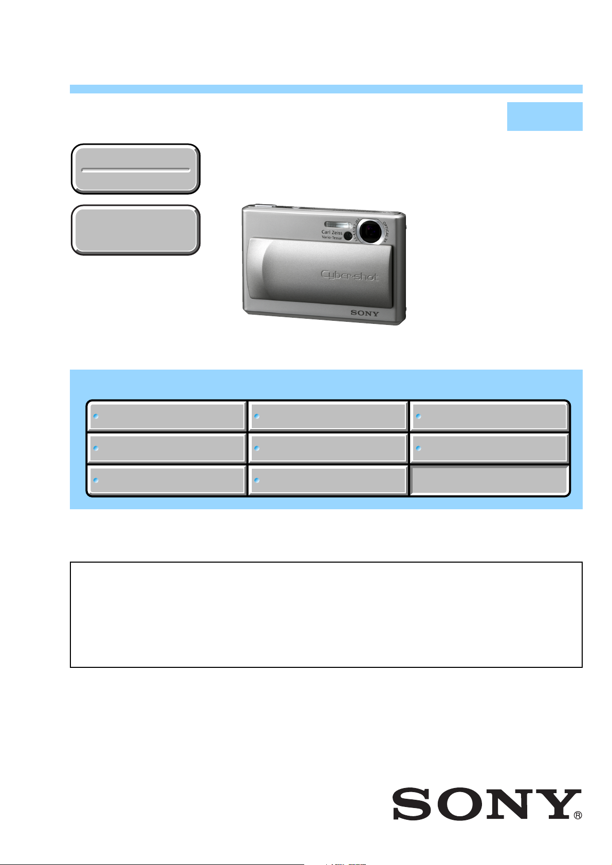
DSC-T1
SERVICE MANUAL
Ver 1.0 2003. 10
Revision History
Revision History
How to use
How to use
Acrobat Reader
Acrobat Reader
Link
Link
SPECIFICATIONS
BLOCK DIAGRAMS
BLOCK DIAGRAMS
LEVEL 2
US Model
Canadian Model
AEP Model
UK Model
E Model
Hong Kong Model
Australian Model
K orea Model
Chinese Model
Tourist Model
Japanese Model
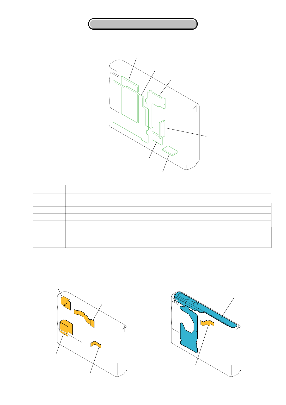
PRINTED WIRING BOARDS
PRINTED WIRING BOARDSSPECIFICATIONS
SERVICE NOTE
SERVICE NOTE
DISASSEMBLY
DISASSEMBLY
• For ADJUSTMENTS (SECTION 6), refer to SERVICE MANUAL, ADJ (987628051.pdf).
• For INSTRUCTION MANUAL, refer to SERVICE MANUAL, LEVEL 1 (987628041.pdf).
• Reference No. search on printed wiring boards is available.
On the LD-140, MS-148 and SY-95 boards
This service manual provides the information that is premised the circuit board replacement service and not intended repair
inside the LD-140, MS-148 and SY-95 boards.
Therefore, schematic diagram, printed wiring board, waveforms, mounted parts location and electrical parts list of the
MS-148 and SY-95 boards
The following pages are not shown.
Schematic diagram .............................Pages 4-15 to 4-36
Printed wiring board............................Pages 4-45 to 4-52
are not shown.
FRAME SCHEMATIC DIAGRAMS
FRAME SCHEMATIC DIAGRAMS
SCHEMATIC DIAGRAMS
SCHEMATIC DIAGRAMS
Mounted parts location .............................
Electrical parts list................................... Pages 5-7 to 5-11
REPAIR PARTS LIST
REPAIR PARTS LIST
Pages 4-54 to 4-55
LD-140,
DIGITAL STILL CAMERA
Page 2

DSC-T1
x Camera
[System]
Image device
Total pixels number of camera
Effective pixels number of camera
Lens Carl Zeiss Vario-Tessar
Exposure control
White balance
File format (DCF compliant)
Recording media
Flash Recommended distance (ISO set to
[Input and Output connectors]
Multi connector
[LCD screen]
LCD panel
Total number of dots
7.66 mm (1/2.4 type) color CCD
Primary color filter
Approx. 5 255 000 pixels
Approx. 5 090 000 pixels
3× zoom lens
f = 6.7 – 20.1 mm (38 – 114 mm when
converted to a 35 mm still camera)
F3.5 – 4.4
Automatic exposure, Scene selection
(8 modes)
Automatic, Daylight, Cloudy,
Fluorescent, Incandescent, Flash
Still images: Exif Ver. 2.2 JPEG
compliant, DPOF compatible
Audio with still image: MPEG1
compliant (Monaural)
Movies: MPEG1 compliant
(Monaural)
“Memory Stick Duo”
Auto):
0.3 m to 1.5 m (11 7/8 inches to
59 1/8 inches) (W)
0.5 m to 1.5 m (19 3/4 inches to
59 1/8 inches) (T)
6.2 cm (2.5 type) TFT drive
211200 (960×220) dots
SPECIFICATIONS
[General]
Used battery pack
Power requirements
Power consumption (during shooting)
Operating temperature
Storage temperature
Dimensions
Mass Approx. 180 g (6.3 oz) (including
Built-in microphone
Built-in speaker
Exif Print Compatible
PRINT Image Matching II Compatible
xUC-TA USB cradle
[Input and Output connectors]
A/V OUT (MONO) jack (Monaural)
USB jack B
USB connection
DC IN jack
Camera connector
NP-FT1
3.6 V
1.6 W
0°C to +40°C (+32°F to +104°F)
–20°C to +60°C (–4°F to +140°F)
91 × 60 × 21 mm
(3 5/8 × 2 3/8 × 2 7/32 inches)
(W/H/D, excluding maximum
protrusions)
battery pack NP-FT1, “Memory Stick
Duo” and wrist strap)
Electret condenser microphone
Piezo-electric speaker
Minijack
Video: 1 Vp-p, 75 Ω, unbalanced,
sync negative
Audio: 327 mV (at a 47 kΩ load)
Output impedance 1 kΩ
High-Speed USB
(USB 2.0 High-Speed compatible)
x AC-LM5 AC Adaptor
Power requirements
Current consumption
Power consumption
Rated output voltage
Operating temperature
Storage temperature
Dimensions
Mass Approx. 170 g (6.0 oz) excluding
100 to 240 V AC, 50/60 Hz
0.2 A
10 W
4.2 V DC, 1.5 A
0°C to +40°C (+32°F to +104°F)
–20°C to +60°C (–4°F to +140°F)
Approx. 47 × 30 × 80mm
(1 7/8 × 1 3/16 × 31/4 inches)
(W/H/D, excluding projecting parts)
power cord (mains lead)
x NP-FT1 battery pack
Used battery
Maximum voltage
Nominal voltage
Capacity 2.4 Wh (680 mAh)
Lithium-ion battery
DC 4.2 V
DC 3.6 V
x Accessories
• AC-LM5 AC Adaptor (1)
• Power cord (mains lead) (1)
• UC-TA USB cradle (1)
• USB cable (1)
• NP-FT1 battery pack (1)
• A/V connecting cable (1)
• Wrist strap (1)
• “Memory Stick Duo” (32 MB) (1)
• Memory Stick Duo Adaptor (1)
• CD-ROM (USB driver SPVD-013) (1)
• Operating instructions (1)
— 2 —
Design and specifications are subject to change
without notice.
Page 3

CAUTION :
Danger of explosion if battery is incorrectly replaced.
Replace only with the same or equivalent type.
DSC-T1
SAFETY-RELATED COMPONENT WARNING!!
COMPONENTS IDENTIFIED BY MARK 0 OR DOTTED LINE WITH
MARK 0 ON THE SCHEMATIC DIAGRAMS AND IN THE PARTS
LIST ARE CRITICAL TO SAFE OPERATION. REPLACE THESE
COMPONENTS WITH SONY PARTS WHOSE PART NUMBERS
APPEAR AS SHOWN IN THIS MANUAL OR IN SUPPLEMENTS
PUBLISHED BY SONY .
SAFETY CHECK-OUT
After correcting the original service problem, perform the following
safety checks before releasing the set to the customer.
1. Check the area of your repair for unsoldered or poorly-soldered
connections. Check the entire board surface for solder splashes
and bridges.
2. Check the interboard wiring to ensure that no wires are
"pinched" or contact high-wattage resistors.
3. Look for unauthorized replacement parts, particularly
transistors, that were installed during a previous repair. Point
them out to the customer and recommend their replacement.
4. Look for parts which, through functioning, show obvious signs
of deterioration. Point them out to the customer and
recommend their replacement.
5. Check the B+ voltage to see it is at the values specified.
6. Flexible Circuit Board Repairing
• Keep the temperature of the soldering iron around 270˚C
during repairing.
• Do not touch the soldering iron on the same conductor of the
circuit board (within 3 times).
• Be careful not to apply force on the conductor when soldering
or unsoldering.
ATTENTION AU COMPOSANT AYANT RAPPORT
À LA SÉCURITÉ!
LES COMPOSANTS IDENTIFÉS P AR UNE MARQUE 0 SUR LES
DIAGRAMMES SCHÉMA TIQUES ET LA LISTE DES PIÈCES SONT
CRITIQUES POUR LA SÉCURITÉ DE FONCTIONNEMENT. NE
REMPLACER CES COMPOSANTS QUE PAR DES PIÈSES SONY
DONT LES NUMÉROS SONT DONNÉS DANS CE MANUEL OU
DANS LES SUPPÉMENTS PUBLIÉS PAR SONY.
Unleaded solder
Boards requiring use of unleaded solder are printed with the leadfree mark (LF) indicating the solder contains no lead.
(Caution: Some printed circuit boards may not come printed with
the lead free mark due to their particular size.)
: LEAD FREE MARK
Unleaded solder has the following characteristics.
• Unleaded solder melts at a temperature about 40°C higher than
ordinary solder.
Ordinary soldering irons can be used but the iron tip has to be
applied to the solder joint for a slightly longer time.
Soldering irons using a temperature regulator should be set to
about 350°C.
Caution: The printed pattern (copper foil) may peel away if the
heated tip is applied for too long, so be careful!
• Strong viscosity
Unleaded solder is more viscous (sticky, less prone to flow) than
ordinary solder so use caution not to let solder bridges occur such
as on IC pins, etc.
• Usable with ordinary solder
It is best to use only unleaded solder but unleaded solder may
also be added to ordinary solder.
— 3 —
Page 4

DSC-T1
TABLE OF CONTENTS
1. SERVICE NOTE ........................................................1-1
2. DISASSEMBLY
2-1. DISASSEMBLY······························································2-1
2-2. SERVICE POSITION ·····················································2-3
2-3. CIRCUIT BOARDS LOCATION···································2-5
2-4. FLEXIBLE BOARDS LOCATION ································2-5
HELP (List of caution points is shown here.)
3. BLOCK DIAGRAMS
3-1. OVERALL BLOCK DIAGRAM (1/2) ··························· 3-1
3-2. OVERALL BLOCK DIAGRAM (2/2) ··························· 3-3
3-3. POWER BLOCK DIAGRAM (1/2) ································3-5
3-4. POWER BLOCK DIAGRAM (2/2) ································3-7
4. PRINTED WIRING BOARDS AND
SCHEMATIC DIAGRAMS
4-1. FRAME SCHEMATIC DIAGRAM (1/2)·······················4-1
FRAME SCHEMATIC DIAGRAM (2/2)·······················4-3
4-2. SCHEMATIC DIAGRAMS
• CD-463 (CCD IMAGER)
SCHEMATIC DIAGRAM ······························4-7
• CN-198 (MULTI CONNECTOR)
SCHEMATIC DIAGRAM ······························4-9
• ST-86 (FLASH)
SCHEMATIC DIAGRAM ····························4-11
• CONTROL SWITCH BLOCK (PW-125)
SCHEMATIC DIAGRAM ····························4-13
5. REPAIR PARTS LIST
5-1. EXPLODED VIEWS ······················································5-1
5-1-1. OVERALL SECTION····················································5-3
5-1-2.BATTERY HOLDER SECTION ····································5-4
5-1-3.CABINET (REAR) SECTION ·······································5-5
5-2. ELECTRICAL PARTS LIST ··········································5-6
Parts list of the SY-95, MS-148 and LD-140 boards
are not shown.
Pages from 5-7 to 5-11 are not shown.
Shematic diagram of the SY-95, MS-148 and LD-140
boards are not shown.
Pages from 4-15 to 4-36 are not shown.
4-3. PRINTED WIRING BOARDS
• CD-463 (CCD IMAGER)
PRINTED WIRING BOARD ·······················4-41
• ST-86 (FLASH)
PRINTED WIRING BOARD ·······················4-42
• CN-198 (MULTI CONNECTOR)
PRINTED WIRING BOARD ·······················4-43
Printed wiring board of the
and FP-694 boards
Pages from 4-45 to 4-52 are not shown.
4-4. MOUNTED PARTS LOCATION ·································4-53
Mounted parts location of the SY-95, MS-148
and FP-695 boards are not shown.
Pages from 4-54 to 4-55 are not shown.
SY-95, MS-148, LD-140
are not shown.
— 4 —
Page 5
• NOTE FOR REPAIR
DSC-T1
SECTION 1
SERVICE NOTE
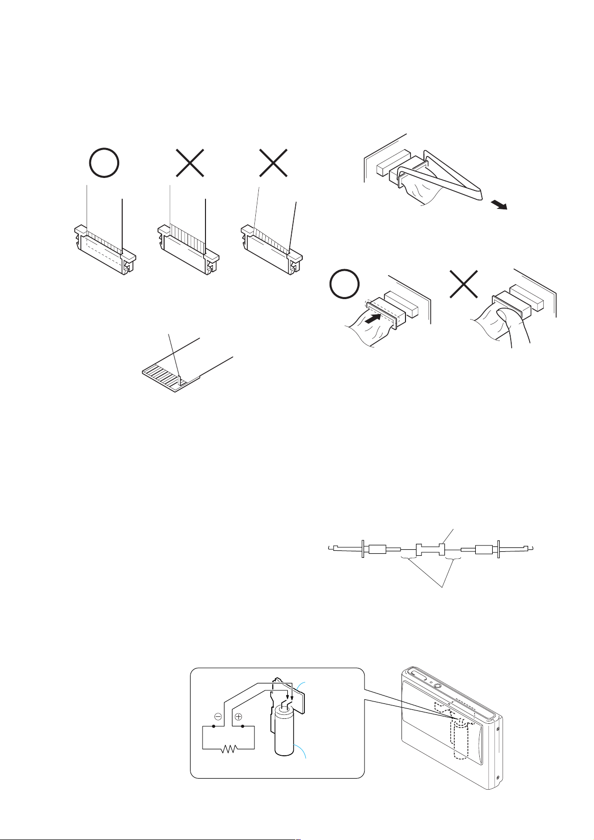
Make sure that the flat cable and flexible board are not cracked of
bent at the terminal.
Do not insert the cable insufficiently nor crookedly.
Cut and remove the part of gilt
which comes off at the point.
(Take care that there are
some pieces of gilt left inside)
When remove a connector, don't pull at wire of connector.
Be in danger of the snapping of a wire.
When installing a connector, don't press down at wire of connector.
Be in danger of the snapping of a wire.
[Discharging of the FLASH unit’s charging capacitor]
The charging capacitor of the FLASH unit is charged up to the
maximum 300 V potential.
There is a danger of electric shock by this high voltage when the
capacitor is handled by hand. The electric shock is caused by the
charged voltage which is kept without discharging when the main
power of the DSC-T1 is simply turned off. Therefore, the remaining
voltage must be discharged as described below.
Preparing the Short Jig
To preparing the short jig. a small clip is attached to each end of a
resistor of 1 kΩ /1 W (1-215-869-11)
Wrap insulating tape fully around the leads of the resistor to prevent
electrical shock.
Discharging the Capacitor
Short circuits between the positive and the negative terminals of
charged capacitor with the short jig about 10 seconds.
1 kΩ/1 W
Wrap insulating tape.
ST-86 B0ARD
Shorting jig
(1kΩ / 1w)
Capacitor
1-1
Page 6

DSC-T1
[Description on Self-diagnosis Display]
Self-diagnosis display
• C: ss: ss
• E: ss: ss
The contents which can be handled
by customer, are displayed.
The contents which can be handled
by engineer, are displayed.
Display Code
C:32:01
C:13:01
E:91:01
E:61:00 *1
E61:10 *1
Note : The error code is cleared if the battery is removed, except defective flash unit.
*1: The error display is given in two ways.
Turn off the main power then back on.
Replace the memory stick.
Format the memory stick with the DSC-T1.
Checking of flash unit or replacement of
flash unit.
Checking of lens drive circuit
Countermeasure
Trouble with hardware.
• The type of memory stick that cannot be
used by this machine, is inserted.
• Data is damaged.
• Unformatted memory stick is inserted.
Abnormality when flash is being
charged.
When failed in the focus initialization.
Cause
Caution Display During Error
SYSTEM ERROR
MS ERROR
Flash LED
Flash display
Flashing at 3.2 Hz
—
1-2E
Page 7

Link
Link
DSC-T1
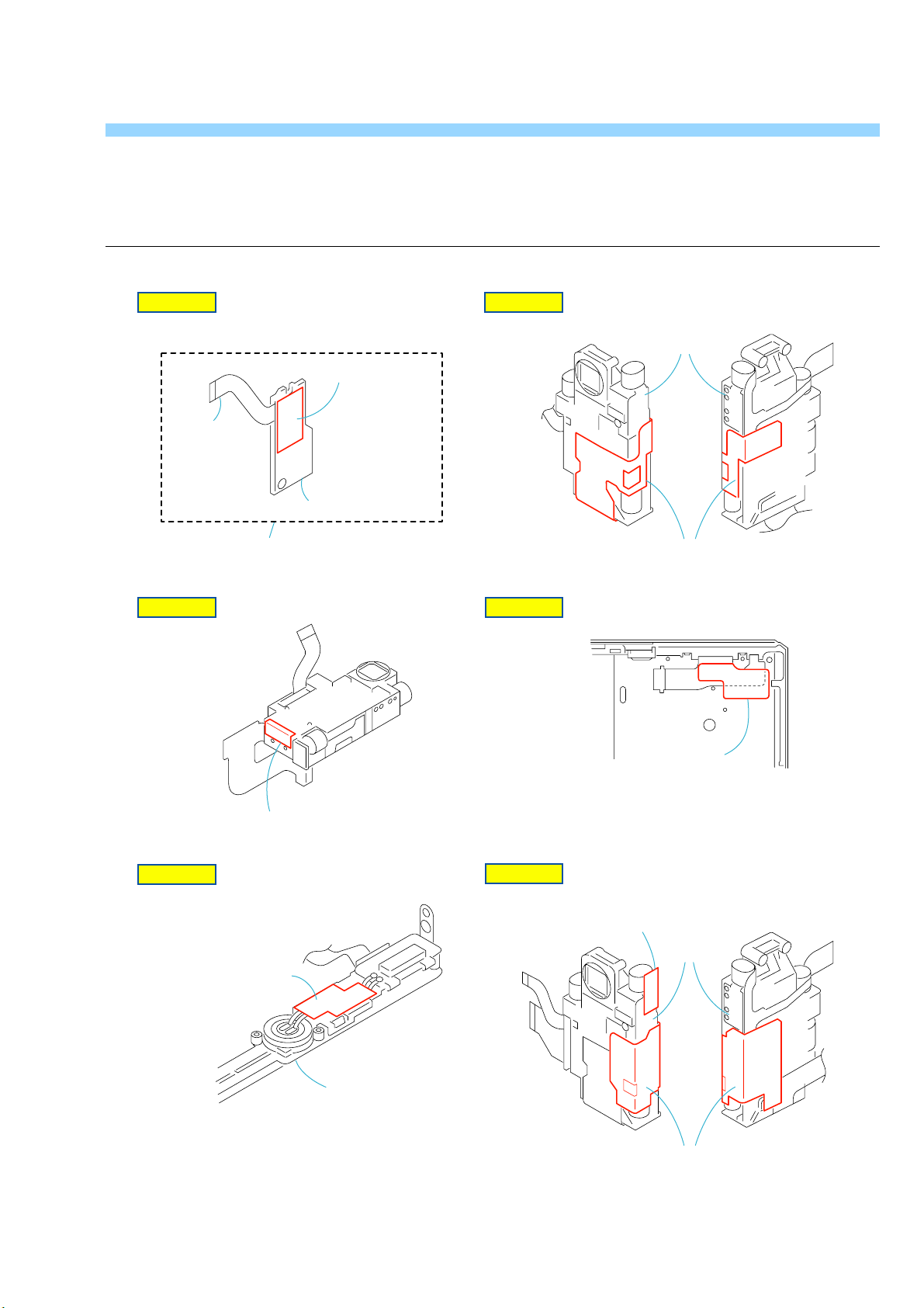
2. DISASSEMBLY
DISASSEMBLY
DISASSEMBLY
SERVICE POSITION FLEXIBLE BOARDS LOCATION
SERVICE POSITION FLEXIBLE BOARDS LOCATION
HELP
HELP
CIRCUIT BOARDS LOCATION
CIRCUIT BOARDS LOCATION
Page 8
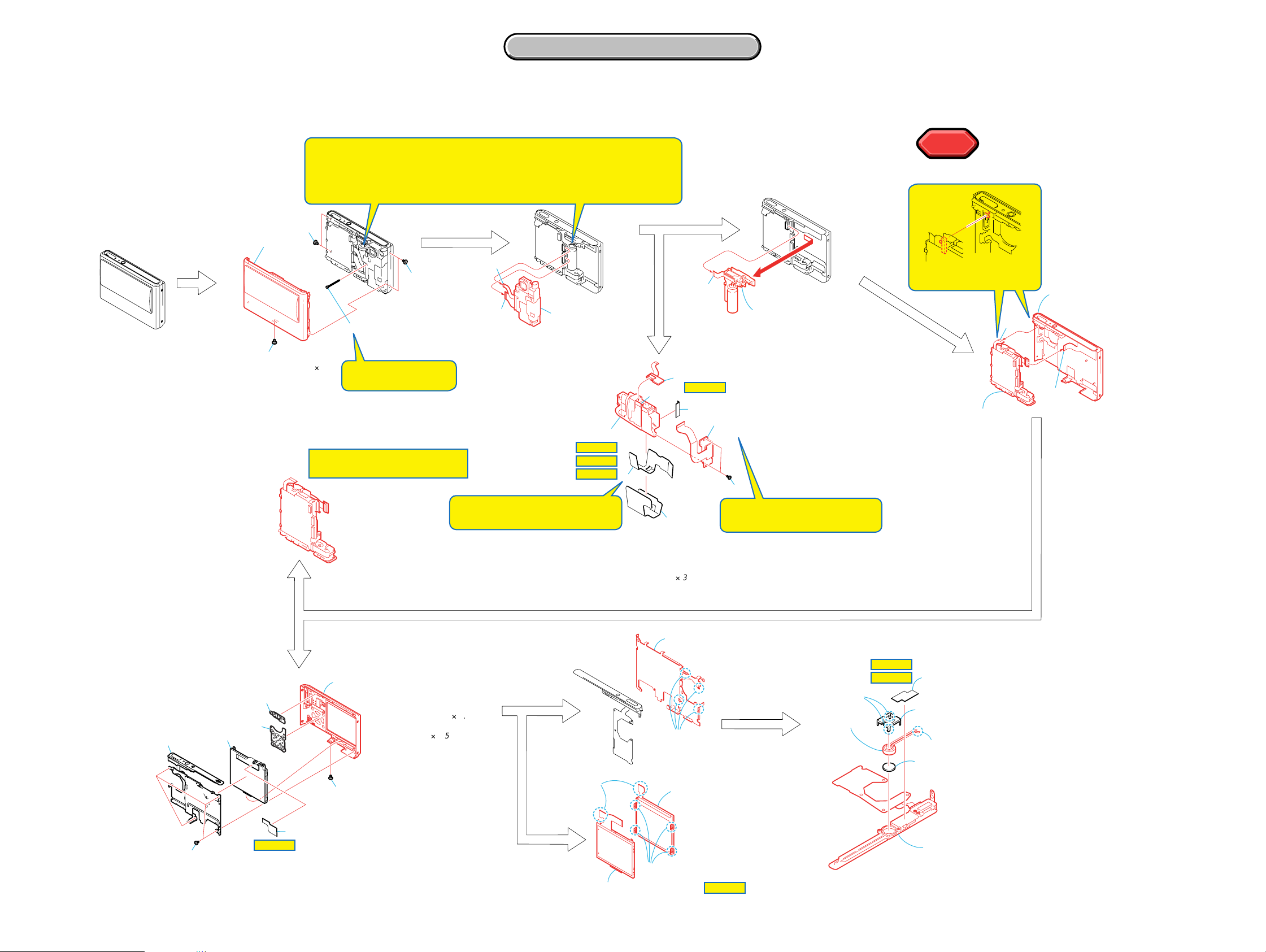
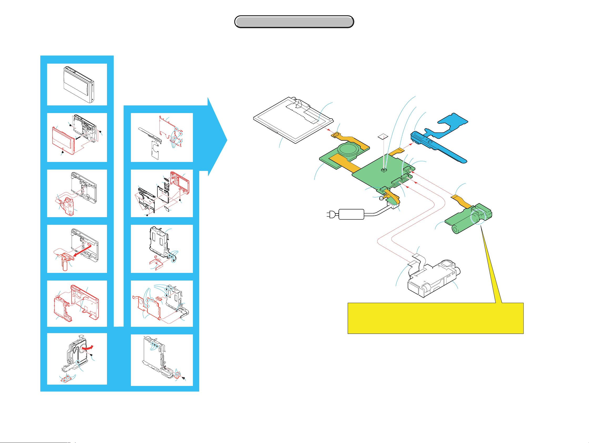
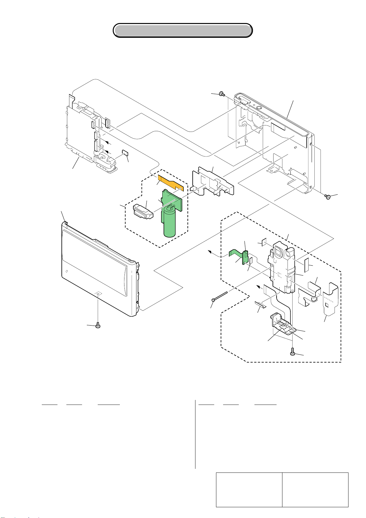
The following flow chart shows the disassembly procedure.
)
2-1. DISASSEMBLY
Note:
1
2
2. DISASSEMBLY
2. DISASSEMBLY
The power capacitor of the flash unit is charged up to 315 V maximum. If you touch
the capacitor terminal that is charged to high voltage, you will receive an electric
shock. This high voltage is not discharged even if you turned off the main power
of this set, and it residues. Discharge the residual voltage referring to the service
note (page 1-1).
HELP
HELP
(Sheet attachment positions and procedures of processing
the flexible boards/harnesses are shown.)
DSC-T1
1
1
Five screws (M1.4 ´ 2.5),
lock ace, p2 (special)
2
Cabinet (front) assembly
3
Lens shaft
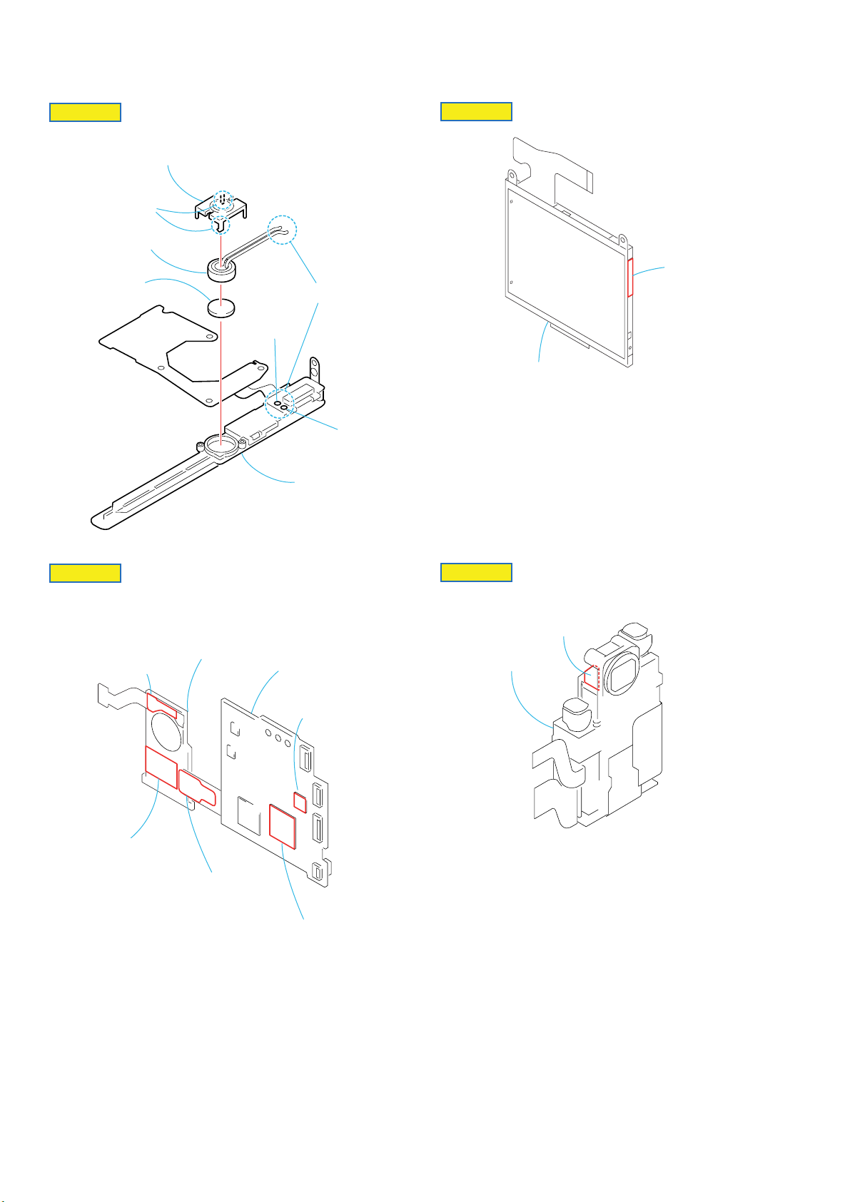
HELP 08
(disassembly of the Battery holder section)
SY-95
1
3
Note:
Be careful not to drop
the lens shaft.
1
2
1
FP-695 board (21P)
2
CCD block
assembly (33P)
Note:
Do not peel off the radiation sheet as
much as possible. If you peel it off, be
careful not to damage the flexible board.
3
Lens section
8
LSV-850A
HELP 02
HELP 03
HELP 06
1
Copper leaf sheet
2
Flexible board (from LSV-850A)(21P)
4
Radiation sheet (CCD)
5
Insulating sheet (CCD)
6
Two tapping screws (B1.2 ´ 3.5)
Note:
When re-assembling,
1
3
FP-695 board (Including the LD-140 board)
2
4
HELP 01
5
7
CCD block
assembly
6
Note:
1
as a single unit since removing it
as a single unit requires adjustment.
1
FP-690 flexible
board (19P)
2
ST-86 board,
ST terminal cover
The CCD imager is not supplied
confirm the switch position.
1
SY-95
3
Battery holder
section
4
Cabinet (rear)
section
2
1
LCD unit
(ACX500EN-J) (25P
2
FP-693 flexible
board (16P)
2
HELP 05
8
Cabinet (rear) assembly
6
7
4
2
5
3
1
HELP 04
1
T ape (LCD)
2
Four screws (M1.4 ´ 2.5),
lock ace, p2 (special)
3
Screw (M1.4 ´ 2.5),
lock ace, p2 (special)
4
Control switch block,
LCD frame, etc.
5
LCD unit (ACX500EN-J)
Block light guide plate
6
Zoom button
7
SW button
1
Four claws
LCD frame
2
1
2
3
LCD unit (ACX500EN-J)
1
4
Block light guide plate
1
Remove the solderings
Four claws
2
HELP 09
5
Microphone
HELP 07
2
1
1
Harness protection sheet
2
T wo claws
3
3
6
Microphone holder
4
T wo solderings
6
Microphone cushion
4
7
Control switch block (PW-125)
2-1 2-2
Page 9
DSC-T1
2-2. SERVICE POSITION
2. DISASSEMBLY
2. DISASSEMBLY
[SERVICE POSITION TO CHECK THE SY-95 BOARD]
Note1: By using an adhesive tape, press the LENS COVER switch (S401).
Note2: When checking the VIDEO AMP (SY-95 board IC302) or the USB circuit, connect the cradle.
(25P)
FP-693 flexible board (16P)
Control switch block (PW-125)
S401 LENS COVER switch (Note1)
1
2
3
1
1
2
CN402
1
LCD unit (ACX500EN-J),
Block light guide plate
CN701
CN703
SY-95 board
CN704
CN705
SY-95
FP-690
flexible board (19P)
CN702
CN-198 board
ST-86 board
6
7
4
1
2
3
5
2
8
MS-148 board
3
1
AC IN
3
AC power
adaptor
FP-695 board (21P)
1
1
3
SY-95
2
1
4
2
2
2
SY-95
3
4
Note :
CCD block
assembly (33P)
Lens section
The power capacitor of the flash unit is charged up to 315 V maximum. If you touch
the capacitor terminal that is charged to high voltage, you will receive an electric
5
1
shock. This high voltage is not discharged even if you turned off the main power
of this set, and it residues. Discharge the residual voltage referring to the service
note (page 1-1).
5
4
3
2
4
2
1
3
1
2-3 2-4
Page 10
2. DISASSEMBLY
NAME FUNCTION
CCD IMAGER
MULTI CONNECTOR
LENS DRIVE
MS I/O, LCD PANEL DRIVE
FLASH
CAMERA A/D CONVERTER, TIMING GENERATOR, CAMERA DSP, LENS CONTROL,
CAMERA SYSTEM CONTROL, HI CONTROL, AUDIO I/O, FLASH DRIVE,
DC/DC CONVERTER, CONNECTOR
CD-463
CN-198
LD-140
MS-148
ST-86
SY-95
MS-148
SY-95
ST-86
LD-140
CN-198
CD-463
FP-694
FP-693
FP-690
FP-691
FP-695
CONTROL SWITCH BLOCK
(PW-125)
2. DISASSEMBLY
2-3. CIRCUIT BOARDS LOCATION
DSC-T1
2-4. FLEXIBLE BOARDS LOCATION
The flexible boards contained in the lens block are not shown.
2-5E
Page 11
2003.10.29
HELP
Sheet attachment positions and procedures of processing the flexible boards/harnesses are shown.
DSC-T1
HELP 01
FP-695
flexible board
HELP 03
FP-695 board
HELP 02
LSV-850A
Adhesive sheet (LD)
LD-140 board
Radiation sheet (CCD)
HELP 04
HELP 05
Insulating sheet (CCD)
Harness
protection sheet
Tape (LCD)
HELP 06
Protection sheet (motor)
LSV-850A
Control switch block
(PW-125)
Copper leaf sheet
HELP
Page 12
DSC-T1
)
HELP 07
Microphone
Microphone
cushion
HELP 09
Microphone holder
Two claws
Sheet (BL
Two solderings
(Black)
LCD unit (ACX500EN-J)
(Red)
Control switch block
(PW-125)
HELP 10
MS protection sheet (S)
MS protection sheet (L)
MS-148 board
SY-95
Radiation sheet (D)
SY-95 board
Sheet
Electrostatic sheet (K)
HELP 11
Light interception
sheet (L)
LSV-850A
HELP
Page 13

HELP 08
s
(disassembly of the Battery holder section)
4
Claw
1
T wo claws
2
Cap (multi)
5
3
Screw
(M1.4
lock ace, p2
(special)
×
2.5),
qa
Three claws
9
Remove the
three solderings
8
SY holder
7
T wo claws
6
Screw
×
(M1.4
lock ace, p2
(special)
2.5),
DSC-T1
qg
Remove the
two solderings
SY-95
qh
MS-148 board
SY-95
qf
SY-95 board,
MS-148 board
qs
Battery
terminal board
ql
CN-198 board
qd
CN-198 board (6P)
q;
CN-198 board (19P)
w;
Battery holder
assembly
qk
Three claw
SY-95
qj
SY-95 board
wa
T wo solderings
ws
Lithium battery
wd
CN-198 board
HELP
Page 14

Link
Link
DSC-T1
3. BLOCK DIAGRAMS
OVERALL BLOCK DIAGRAM (1/2)
OVERALL BLOCK DIAGRAM (1/2)
POWER BLOCK DIAGRAM (1/2)
POWER BLOCK DIAGRAM (1/2)
POWER BLOCK DIAGRAM (2/2)OVERALL BLOCK DIAGRAM (2/2)
POWER BLOCK DIAGRAM (2/2)OVERALL BLOCK DIAGRAM (2/2)
Page 15

DSC-T1
BLOCK DIAGRAMS
3-1. OVERALL BLOCK DIAGRAM (1/2)
LENS UNIT
(LSV-850A)
LCD901
2.5INCH
COLOR LCD
PANEL
ND901
BACK
LIGHT
IRIS
SHUTER
FOCUS RESET
SENSOR
ZOOM RESET
SENSOR
FP-694
FLEXIBLE
8
9
7
10
6
11
12
14
16
21
24
1
3
CN402
IRIS
MOTOR
M
FOCUS
MOTOR
M
ZOOM
MOTOR
M
VR
VG
VB
PS1G
RGT,HCK1,2
REF,HST
WIDE,DWN
EN,VCK,
VST
CD-463 BOARD
IC001
CCD IMAGER
1-5,7-9
11-142021-24
V1A,B
V2
V3A,B
V4
V5A,B
V6
V7A,B
V8
15-11,9-7,5-2
X151
54MHz
XTAL
OSC
LD-140 BOARD
IRIS A
IRIS A
G4
IRIS B
18
21
8
11
12
15
5
2
CN002
IRIS B
FOCUS A
FOCUS A
FOCUS B
FOCUS B
ZOOM A
ZOOM A
ZOOM B
ZOOM B
H4
G5
H6
A6
B5
A4
B4
C1
D2
E1
E2
MS-148 BOARD
(1/3)
D6
C7
C6
Q801,802
A7
BUFFER
G2,F3
E4,F4
F7,E5
A3,B3
C3,A2
CN702
TG CLK
IC001
FOCUS MOTOR
ZOOM MOTOR
IC803
RGB DRIVE
TIMING GENERATOR
Note:
The CCD imager is not supplied
as
as a single unit requires adjustment.
17
H1A,B
H2A,B
RG
(1/8)
IC152
FREQUENCY DEVIDER
IRIS DRIVE
DRIVE
DRIVE
(2/2)
C1
C2
B1
D1
D2
F5
E3
F2
F1
A4
A5
SECTION 3
3. BLOCK DIAGRAMS
3. BLOCK DIAGRAMS
( ) : Number in parenthesis ( ) indicates the division number of schematic diagram where the component is located.
SY-95 BOARD(1/2)
a single unit since removing it
Q004
BUFFER
51
FP-695
FLEXIBLE
G1
G2
H2
G3
C8
C7
B8
B7
B3
A2
B2
A1
FP-691
FLEXIBLE
(1/2)
Q805
LPF
18
20
19
15
17
16
12
14
13
11
8
CCD OUT
30
21
22
24
25
27
CN702
CN701
PANEL R
PANEL G
PANEL B
PANEL V
XSYS RST
HDO
86
37
42
48
51
33
10,13
113,17
20,109
112,115
125,119
118,121
84
CAM SO,SCK
EXT CLK
HR EN3
HR DIR3A
HR DIR3B
HR EN2
HR DIR2A
HR DIR2B
HR EN0
HR DIR0A
HR DIR0B
XFC RST SENS
XIR RST SENS
STRB ON
BL LEV
LED A
LED K
S/H
A/D CONV.
(1/8)
IC151
TIMING
GENERATOR
126-129 123,3
1
134,136,2,4,6
9,12,15,18,21
24,27,30,32
64
55
99
49,105
66,101,120
XCAM RST
TO
OVERALL
BLOCK DIAGRAM
(2/2)
(PAGE 3-3)
CA HD
CA F
CA F
V OUT
STRB ON
PANEL R
PANEL G
PANEL B
HDO
PANEL V
CA AD0
CA AD13
CLP DM
CLP OB
MCK TG
CA HD
CA F
HR DIR3A
HR DIR3B
HR EN0
HR DIR0A
HR DIR0B
HR EN2
HR DIR2A
HR DIR2B
XFC RST SENS
XZM RST SENS
Q302-Q304
(2/8)
IC302
VIDEO AMP
BUFFER
(AA,AB,Y)
(AA,AB,AC,
MC D0-D15
A18
Y18
AC16
(2/8)
IC301
CAMERA
Y17
AB18
N21
L21
P21
K20
L22
J21
M21
M20
N20
F21
F20
AB4
E23
C23
D23
C18
D17
F23
42
XSYS RST
DSP
T20
U,V,W,Y)
(J,K,L,M,
N,P,R,T,U)
D16
T23
AA7
AC12
AC9
MC A1-A25
SYS V
MC CKIO
AU LRCK
AU A IN
AU A OUT
CAM SO,SCK
SYS SO,SI,SCKSYS SO,SI,SCK
XCAM RST
CA F
EXT CLK
(J,M,N,P
R,T,V,M)
(21-24)
(E-H,
J-M)
(21-24)
AA8
A7
H1
C7
C23
AC12
A6
B11
A11
C11
A12
B12
(3/8)
IC501
CAMERA
SYSTEM
CONTROL
AB13
AD19
AC15
AB11
AD14
B16
C15
A15
D15
B15
D16
C22
D13
B13
C13
K2
D14
AB5
L4
F1
H23
V1
W1
AB7
MS SDIO/DATA0-3,MS BS, MS SCLK
XACCESS LED
XMS IN
SYS V
FR SO,SI,SCK
XSYS RST
XAE LOCK ON
XSHTR ON
STRB CHG
XSTRB FULL
XSTRB PWR ON
XUSB JACK IN
Q504
PRELAMP AF CONT
SELF TIMER LED
USBPHY D+,D-
MELODY
MELODY EW
Q501
MOD
AU A IN
AU A OUT
BEEP
2
E1
H4
H5
FP-691
FLEXIBLE
(2/2)
TO
OVERALL
BLOCK DIAGRAM
(2/2)
(PAGE 3-4)
(5/8)
IC601
AUDIO
AMP
MS-148
BOARD(2/3)
4,3,5,7,
2,8
LED DRIVE
D103
Q102
SP+
SP-
(ACCESS)
CN101
MEMORY
STICK
DUO
6
CONNECTOR
SP901
SPEAKER
CN-198
BOARD(1/2)
CN704
9
8
CN001
MIC IN
AU OUT
V OUT
MIC901
MIC
B4
A2
D1
B8
4
2
1
CONTROL SWITCH
BLOCK(PW-125)
(1/2)
AUDIO SIGNAL
VIDEO SIGNAL
VIDEO/AUDIO SIGNAL
10
12
CN001
MULTI
CONNECTOR
16
17
3-1 3-2
Page 16

DSC-T1
3. BLOCK DIAGRAMS
3. BLOCK DIAGRAMS
3-2. OVERALL BLOCK DIAGRAM (2/2)
MS-148 BOARD
(3/3)
S101
MODE SW
FP-691
FLEXIBLE
CN-198 BOARD
CN001
MULTI
CONNECTOR
11
13
14
24
3
2
1
(2/2)
VBUS
XMULTI JACK IN
XAV JACK IN
BATT/XEXT
ACV UNREG
BT901
BATTERY
TERMINAL
BT001
LITHIUM
BATTERY
(SECONDARY)
C
Q002
8 1
5
4
( ) : Number in parenthesis ( ) indicates the division number of schematic diagram where the component is located.
SY-95 BOARD
(2/2)
CN704
VL 3V
11
12
13
14
15
18
17
4
5
6
CN705
F002
F003
F001
D015 D013
D8
D011
A10
B11
D9
OUT8A
E9
OUT8B
D1
D036
E5
D4
E4
USB JACK IN
3V
REG
BATTERY
CHARGER
FET DRIVE
(7/8)
IC001
DC/DC CONVERTER
(7/8)
IC003
ST UNREG
ACV UNREG
BATT UNREG
RESET
BATTERY IN
DETECT
Q406
LENS COVER
()
L8
K8
XRSTX
B7
BACK UP VCC
B9
A11
EVER 3.0V
BATT IN
A7
INIT CHARGE
D2
FAST CHARGE
E3
C7
SYS DD ON
D7
S401
OPEN
BATT SIG
DDCON SO,SCK
A 3.1V
D 1.2V
AU 2.8V
D 2.8V
A 2.8V
CAM 15.0V
CAM -8.0V
M 5V
ST 5V
STRB ON
BL LEV
LED A
LED K
CAM -0.5V
X402
32.768KHz
Q407
I/F
1
J8
B7
J4
J5
C8
C4
A3
A7
G2
G1
J1
H2
E8
C1
D3
D7
A5
H4
A9
TO
OVERALL
BLOCK DIAGRAM
(1/2)
(PAGE 3-1)
MODE DIAL
XLENZ CAP OPN
32KHz IN
32KHz OUT
XUSB JACK IN
XMULTI JACK IN
XAV JACK IN
BATT/XEXT
BATT SI
BATT SO
INIT CHARGE
FAST CHARGE
SYS DD ON
DDCON SO
DDCON SCK
XRSTX
BACK UP VCC
BATT IN
(4/8)
IC491
HI CONTROL
KEY AD0
KEY AD1
KEY AD2
XPOWER ON
XPWR LED ON
XCHARGE/XSTB LED
MS IN
FR SO
FR SI
XFR SCK
XSYS RST
SYS V
J6
H6
G6
B8
B2
B1
XAE LOCK ON
XSHTR ON
XUSB JACK IN
Q404
B6
D2
D1
E1
B3
B9
XMS IN
FR SO,SI,SCK
XSYS RST
SYS V
STRB CHG
XSTRB PWR ON
XSTB FULL
SELF TIMER LED
PRE LAMP AF CONT
STRB CHG
XSTRB PWR ON
XSTRB FULL
ST UNREG
Q651,652
(6/8)
Q653
(2/2)
IC651
STRB ON
SELF TIMER LED
PRE LAMP AF CONT
IGBT DRIVE
Q701
LED DRIVE
Q653
(1/2)
2
24
XAE LOCK ON
XSHTR ON
TO
OVERALL
BLOCK DIAGRAM
(1/2)
(PAGE 3-2)
CN703
FP-693
FLEXIBLE
FP-690
FLEXIBLE
1
6
15
16
17
19
CONTROL SWITCH
BLOCK(PW-125) (2/2)
12
13
14
5
7
8
3
10
9
CN001
S003-011,013
ZOOM,MENU,IMAGE SIZE/DELETE
DISPLAY/LCD BACK LIGHT,
UP,DOWN,RIGHT, LEFT,SET
S001
POWER
S002
SHUTTER
(POWER)
S012
RESET
ST-86 BOARD
Q001,002
T002
HIGH
XE A(H)
VOLTAGE
CHARGER
Q003
XE K(L)
FLASH
DRIVE
D003
(AF LED)
D004
D003
C003
/CHG
XENON
TUBE
(7/8)
IC007
D 1.8V
3-3 3-4
Page 17

3. BLOCK DIAGRAMS
3. BLOCK DIAGRAMS
DSC-T1
3-3. POWER BLOCK DIAGRAM (1/2)
CN-198
BOARD
1
2
3
24
C
ACV UNREG
BATT/XEXT
BT001
LITHIUM
BATTERY
(SECONDRY)
BATT UNREG
BATT SIG
Q407
I/F
CONTROL
SWITCH
BLOCK
(PW-125)
S001
POWER
D004
D003
S012
RESET
(POWER)
/CHG
CN001
FP-693
FLEXIBLE
5
4
3
11
10
9
CN001
MULTI
CONNECTOR
BT901
BATTERY
TERMINAL
( ) : Number in parenthesis ( ) indicates the division number of schematic diagram where the component is located.
SY-95 BOARD(1/2)
BATT UNREG
ACV UNREG
EVER 3.0V
A5
H4
D7XRST X
A9BATT IN
C1
D3
H1
E8SYS DD ON
J1
H2
F8
F001
F002
F003
DDCON SO,SCK,XCS
ST UNREG
ACV UNREG
INIT CHARGE
FAST CHARGE
D013
D015
L002
L001
D011
D1
D4
E5
D2
E4
E3
E9
D9
B11
A11
A10
D8
B9
B7
A7
L8
K8
K7
C7
D7
BATTERY
CHARGER
OUT8A
OUT8B
3V REG
RESET
DIN
CLK
LD
SYS DD ON
FET
DRIVE
(7/8)
IC001
DC/DC CONVERTER
BATTERY IN
DETECT
VCC1A
VCC1B
VCC1C
OUT11A
OUT11B
OUT11C
OUT12A
OUT12B
OUT12C
VCH1A
VCH1B
VCH1C(FB4)
OUT2
VCH2
OUT3A
OUT3B
OUT3C
VCH3A(FB3)
VCH3B
VCH3C(FB6)
G11
G10
G9
H11
L006
H10
J11
L11
K10
J9
L10
K9
L9
F9VCC2
F10
E11
J3
K1
J2
J1
H4
H3
H2VCH3S
H1VCC GD
K6OUT4
J6VCH4
K5VCC5
L5OUT5
J5VCH5
F1OUT6
G1VCH6
G2ICH6
B1REF6
B5CBG
C8VLD04
B8VLD05
L005
L009
D026
(RECT)
L007
D017
(RECT)
D023
(RECT)
D021
(RECT)
D025
(RECT)
L008
L004
PANEL 13.5V
VL 3V
CN705
4
5
FB701
6
17
11
CN704
H8 BATT SENS
G8 ACV SENS
A7
BATT/XEXT
G2 BATT SI
G1
BATT SO
XPWR ON
B8
XPOWER LED ON
B2
B1
XCHARGE/XSTRB LED
(4/8)
IC491
HI CONTROL
BATT UNREG
Q002
8
4
BACK UP VCC
DDCON SO
DDCON SCK
XCS DD CON
INIT CHARGE
FAST CHARGE
DDCON SENS
1
5
LED A
LED K
BL LV
ST UNREG
LED A
LED K
BL LV
PANEL 13.5V
(7/8)
IC007
1.8V REG
L003
L010
32
AV 2.8V
A 2.8V
D 2.8V
D 1.8V
D 1.2V
1
TO
POWER
BLOCK DIAGRAM
(2/2)
(PAGE 3-7)
M 5V
ST 5V
CAM 15.0V
CAM -8.0V
8 4
VCC+
VCC-
3
2
1
(7/8)
SHUNT
REG
Q001
CAM -0.5V
IC003
-0.5V REG
A 3.1V
D 1.2V
3-5 3-6
Page 18

DSC-T1
3. BLOCK DIAGRAMS
3. BLOCK DIAGRAMS
3-4. POWER BLOCK DIAGRAM (2/2)
SY-95 BOARD(2/2)
ST UNREG
LED A
LED K
BL LV
PANEL 13.5V
AV 2.8V
A 2.8V
D 2.8V
D 1.8V
D 1.2V
TO
POWER
1
BLOCK DIAGRAM
(1/2)
(PAGE 3-6)
( ) : Number in parenthesis ( ) indicates the division number of schematic diagram where the component is located.
D 2.8V
MS PWR ON
PANEL 13.5V
D 2.8V
AV 2.8V
(5/8)
BL LEV
IC601
ST 5V
A 3.1V
A 2.8V
AUDIO AMP
(3/8)
IC501
CAMERA
SYSTEM
CONTROL
(2/8)
IC302
VIDEO AMP
AD18
AD51
AB11
AC15
AC20
F22
MS PWR ON
STRB CHG
XSTRB PWR ON
XSTRB FULL
CAM DD ON
AMP OUT ON
Q305,306
Q302-304
PANEL
R,G,B
BUFFER
LED A
LED K
ST UNREG
STRB CHG
XSTRB PWR ON
XSTRB FULL
Q651,652
Q653
Q655,656
MT 5V
CN703
1
6
15
16
18
FLEXIBLE
FP-690
FLEXIBLE
MS-148 BOARDFP-691
Q101
IC803
RGB DRIVE
TIMING GENERATOR
A5
A4
Q001,002,T002
HIGH
VOLTAGE
CHARGER
D003
AF LED
ST-86 BOARD
VCC
C003
XE A(H)
9
CN101
MEMORY
STICK DUO
CONNECTOR
FP-694
FLEXIBLE
XENON
TUBE
CN402
LCD901
2.5INCH
COLOR LCD
20
1
3
UNIT
(ACX500EN-J)
ND901
BACK LIGHT
M 5V
ST 5V
CAM 15V
CAM -8.0V
CAM -0.5V
A 3.1V
D 2.8V
A 2.8V
AU 2.8V
A 2.8V
D 2.8V
D 1.2V
Q151,152
IC301
CAMERA
IC152
FREQUECY
DEVIDER
CAM DD ON
IC151
S/H,A/D CONV.
TIMING
GENERATOR
(2/8)
DSP
(1/8)
(1/8)
XFC RST LED
J22
XZM RST LED
V21
54MHz
XTAL
OSC
X151
CN702
33
17
IC001
CCD
IMAGER
CD-463 BOARD
Note:
The CCD imager is not supplied
as a single unit since removing it
as a single unit requires adjustment.
(6/8)
IC651
IGBT DRIVE
XFC RST LED
XZM RST LED
Q702
Q702
M 5V
D 2.8V
CN701
1
2
3
7
10
FP-695
FLEXIBLE
IC001
IRIS/FOCUS/
ZOOM DRIVE
F RST VCC
Z RST VCC
LD-140 BOARD
CN002
6
3
LENS UNIT
(LSV-850A)
FOCUS
RESET
SENSOR
ZOOM
RESET
SENSOR
3-7 3-8E
Page 19

SECTION 4
PRINTED WIRING BOARDS AND SCHEMATIC DIAGRAMS
4-1. FRAME SCHEMATIC DIAGRAM (1/2)
1
A
FRAME SCHEMATIC DIAGRAM(1/2)
B
C
D
CD-463 BOARD
E
F
4-2. SCHEMATIC DIAGRAMS 4-3. PRINTED WIRING BOARDS
4-2. SCHEMATIC DIAGRAMS 4-3. PRINTED WIRING BOARDS
810 137
11
129
SY-95 BOARD(1/2)
33PCN702
1REG_GND
2V8
3V7B
4V7A
5V6
6VHLD
7V5B
8V5A
9V4
10VST
11V3B
12V3A
13V2
14V1B
15V1A
16REG_GND
17CAM_-8.0V_CD
18VSUB_CONT
19SHT
20REG_GND
21H1A
22H1B
23REG_GND
24H2A
25H2B
26REG_GND
27RG
28REG_GND
29REG_GND
30CCD-OUT
31REG_GND
32POWER_SAVE
33CAM_15V_CD
MS-148 BOARD
DSC-T1
144 1763
25P
CN402
1 LED_A
ND901
2 N.C.
3 LED_K
4 BL_THH
5 BL_THL
6 RGT
7VB
8VR
9VG
10 PSIG
11 HCK1
12 HCK2
13 CREXT
14 REF
15 HST
16 WIDE
17 REG_GND
18 VDDG
19 VSS
20 VDD
21 DWN
22 EN
23 VCK
24 VST
25 COM
FP-694
FLEXIBLE
BACK LIGHT
LCD901
2.5INCH
COLOR
LCD UNIT
(ACX500EN-J)
1825 15 16
19P
CN704
1REG_GND(AU)
CN705
2V_OUT
3REG_GND(AU)
4AU_OUT
5REG_GND(AU)
6REG_GND(USB)
7REG_GND(USB)
8USBPHY_D-
9USBPHY_D+
10REG_GND(USB)
11VL_3V
12VBUS
13VBUS
14VBUS
15XMULTI_IN
16NC
17BATT/XEXT
18XAV_JACK_IN
19NC
6P
1ACV_GND
2ACV_GND
3ACV_GND
4
5
6
FP-691
FLEXIBLE
1
2
3
4
5
6
7
8
9
10
CN101
GND
BS
DATA1
SDIO/DATA0
DATA2
INT
DATA3
SCLK
VCC
GND
10P
MEMORY
STICK
DUO
CONNECTOR
G
26PCN001
1
ACV_UNREG
ACV_UNREG
3
5
XLANC_JACK_IN
7
USB_LED
9
H
I
11
13
15
17
19
21
23
25
USB_HOST
USB_VBUS
XMULTI_IN
EXT_STRB_ON
V_OUT
V_GND
AUX
ACV_GND
ACV_GND
J
272829
MULTI CONNECTOR
2
ACV_UNREG
4
LANC_DC
6
LANC_SIG
XAV_JACK_IN
A_OUT_L
A_OUT_R
A_GND
BATT/XEXT
ACV_GND
8
10
D+
12
D-
AUX
14
16
18
20
22
24
26
CN-198 BOARD
BT001
LITHIUN BATTERY
(SECONDARY)
ACV_UNREG0
ACV_UNREG0
ACV_UNREG0
USB/LANC_GND
30
16
4-1 4-2
FRAME SCHEMATIC DIAGRAM (1/2)
Page 20
DSC-T1
4-2. SCHEMATIC DIAGRAMS 4-3. PRINTED WIRING BOARDS
4-2. SCHEMATIC DIAGRAMS 4-3. PRINTED WIRING BOARDS
FRAME SCHEMATIC DIAGRAM (2/2)
1
A
FRAME SCHEMATIC DIAGRAM(2/2)
25
B
C
D
E
463
ST-86 BOARD FP-690
FLEXIBLE
8107
1MIC_IN
2REG_GND
3XPOWER_LED_ON
4EVER_3.0V
5XPOWER_ON
6REG_GND
16P
CN001
7XAE_LOCK_ON
FP-693
19PCN703
1STB_UNREG
2STB_UNREG
3STB_UNREG
4STB_UNREG
5STB_UNREG
6STB_UNREG
7REG_GND
8REG_GND
9REG_GND
10REG_GND
11REG_GND
12REG_GND
13REG_GND
14REG_GND
15XSTRB_PWR_SAVE
16STB_FULL
17IGBT_ON
18AF_LED_5V
19AF_LED_K
8XSHTR_ON
9XRESET_SW
10XCHARGE/XSTRB_LED
FLEXIBLE
9
11EVER_3.0V
12KEY_AD0
13KEY_AD1
14KEY_AD2
15REG_GND
16NC
CONTROL SWITCH BLOCK
(PW-125)
11
F
G
H
I
LENS UNIT
(LSV-850A)
CN002
FOCUS_B
FOCUS_A
ZOOM_A
ZOOM_B
IRIS_A
IRIS_B
21P
1Z_RST_GND
2Z_RST_SENS
3Z_RST_VCC
4F_RST_GND
5F_RST_SENS
6F_RST_VCC
7N.C
8FOCUS_A
9
10
11FOCUS_B
12
13ZOOM_A
14ZOOM_B
15
16TEMP_OUT
17TEMP_GND
18
19IRIS_A
20
21IRIS_B
FP-695
FLEXIBLE
21PCN701
1M_5V
2M_5V
3D_2.8V
4REG_GND
5REG_GND
6REG_GND
7F_RST_VCC
8XFC_RST_SENS
9LENS_TEMP
10Z_RST_VCC
11XZM_RST_SENS
12HR_EN0
13HR_DIR0B
14HR_DIR0A
15HR_EN2
16HR_DIR2B
17HR_DIR2A
18HR_EN3
19HR_DIR3B
20HI_DIR3A
21XCAM_DR_PS
SY-95 BOARD(2/2)
LD-140 BOARD
J
FRAME SCHEMATIC DIAGRAM (2/2)
16
4-3 4-4
Page 21

Link
Link
DSC-T1
4-2. SCHEMATIC DIAGRAMS
CD-463 BOARD
CD-463 BOARD
CN-198 BOARD
CN-198 BOARD
COMMON NOTE FOR SCHEMATIC DIAGRAMS
COMMON NOTE FOR SCHEMATIC DIAGRAMS
(CCD IMAGER)
(CCD IMAGER)
(MULTI CONNECTOR)
(MULTI CONNECTOR)
ST-86 BOARD
ST-86 BOARD
CONTROL SWITCH BLOCK
CONTROL SWITCH BLOCK
(FLASH)
(FLASH)
(PW-125)
(PW-125)
Page 22
4-2. SCHEMATIC DIAGRAMS
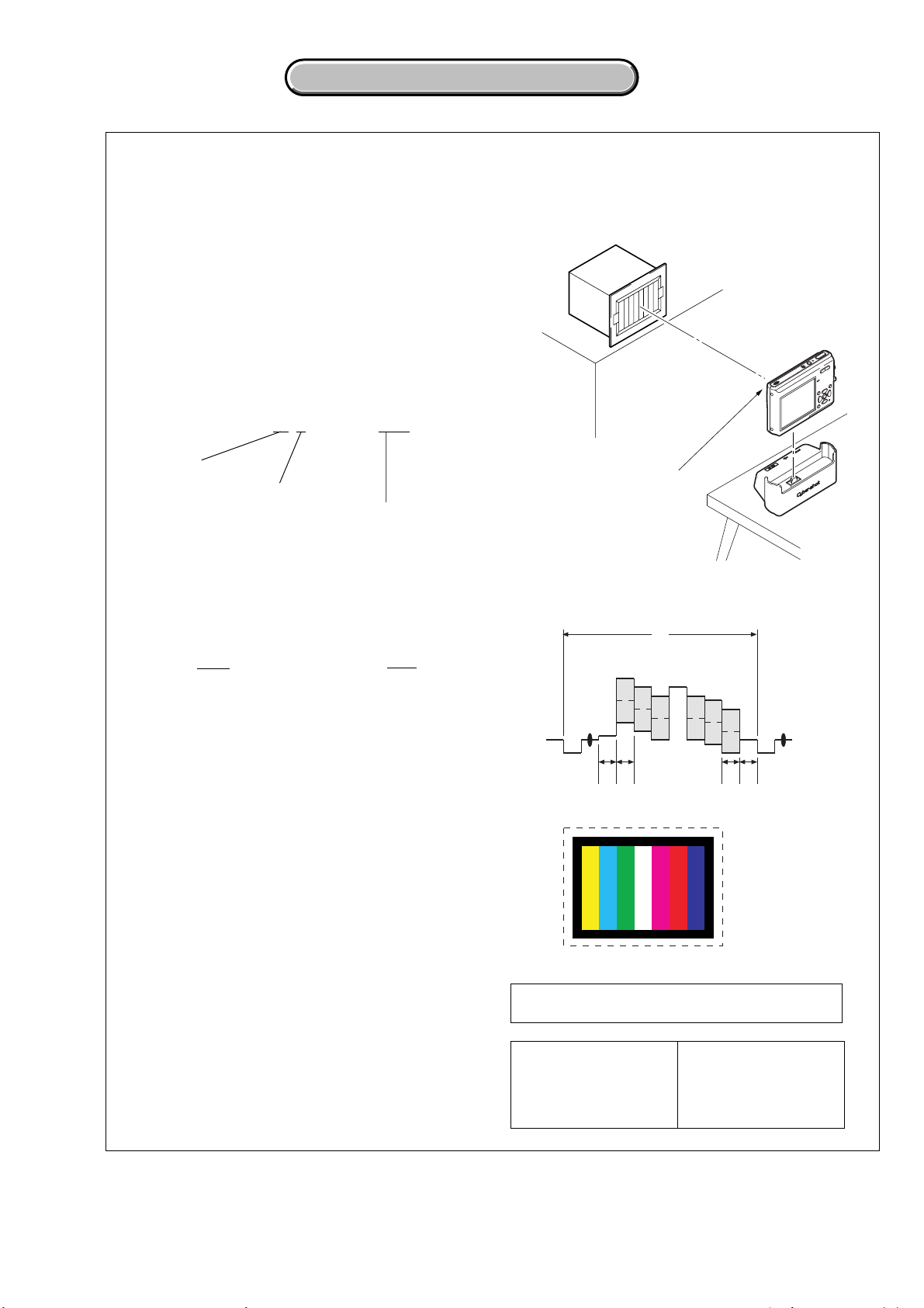
About 30cm
Front of the lens
Pattern box
4-2. SCHEMATIC DIAGRAMS
THIS NOTE IS COMMON FOR SCHEMATIC DIAGRAMS
(In addition to this, the necessary note is printed in each block)
DSC-T1
(For schematic diagrams)
• All capacitors are in µF unless otherwise noted. pF : µ
Link
µF. 50 V or less are not indicated e xcept for electrolytics
and tantalums.
• Chip resistors are 1/10 W unless otherwise noted.
kΩ=1000 Ω, MΩ=1000 kΩ.
• Caution when replacing chip parts.
New parts must be attached after removal of chip.
Be careful not to heat the minus side of tantalum
capacitor, Because it is damaged by the heat.
• Some chip part will be indicated as follows.
Example C541 L452
22U 10UH
TA A 2520
Kinds of capacitor
Temperature characteristics
External dimensions (mm)
• Constants of resistors, capacitors, ICs and etc with XX
indicate that they are not used.
In such cases, the unused circuits may be indicated.
• Parts with * differ according to the model/destination.
Refer to the mount table for each function.
• All variable and adjustable resistors have characteristic
curve B, unless otherwise noted.
• Signal name
XEDIT→ EDIT PB/XREC → PB/REC
• 2: non flammable resistor
• 5: fusible resistor
• C: panel designation
• A: B+ Line
• B: B– Line
• J : IN/OUT direction of (+,–) B LINE.
• C: adjustment for repair.
• A: VIDEO SIGNAL (ANALOG)
• A: AUDIO SIGNAL (ANALOG)
• A: VIDEO/AUDIO SIGNAL (ANALOG)
• A: VIDEO/AUDIO/SER V O SIGNAL
• A: SERVO SIGNAL
• Circled numbers refer to waveforms.
(Measuring conditions voltage and waveform)
• Voltages and waveforms are measured between the
measurement points and ground when camera shoots
color bar chart of pattern box. They are reference values
and reference waveforms.
(VOM of DC 10 MΩ input impedance is used)
• Voltage values change depending upon input
impedance of VOM used.)
1. Connection
2. Adjust the distance so that the output waveform of
Fig. a and the Fig. b can be obtain.
H
Yellow
Cyan
White
Magenta
Green
AABBA=B
Fig. a (Video output terminal output waveform)
Fig.b (Picture on monitor TV)
Red
Blue
When indicating parts by reference number, please
include the board name.
Note :
The components identified by
mark 0 or dotted line with mark
0 are critical for safety.
Replace only with part number
specified.
Note :
Les composants identifiés par
une marque 0 sont critiques
pour la sécurité.
Ne les remplacer que par une
pièce portant le numéro spécifié.
4-5
Page 23

4-2. SCHEMATIC DIAGRAMS CD-463 PRINTED WIRING BOARD
4-2. SCHEMATIC DIAGRAMS CD-463 PRINTED WIRING BOARD
DSC-T1
4-2. SCHEMATIC DIAGRAMS
1
CD-463 BOARD
A
CCD IMAGER
XX MARK:NO MOUNT
NO MARK:REC/PB MODE
B
SIGNAL PATH
C
CHROMA
REC
PB
VIDEO SIGNAL
Y
Y/CHROMA
For Schematic Diagram
• Refer to page 4-41 for printed wiring board.
463
The CCD imager is not supplied
as a single unit since removing it
as a single unit requires adjustment.
IC001
CCD IMAGER
87
6
Vhld
7V48
Vst
V5A9V5B
V3A5V3B
10
11V612
14
V8
V7A13V7B
Rss317CCD-OUT18GND19GND20RG21H2B22H2A23H1B24H1A25GND26SUB27CSUB28VL
15VH16
925
1
3V24
V1A2V1B
ICX473CQZ-13
IC001
D
E
F
G
H
TO
SY-95 BOARD
(1/8)
CN702
(PAGE 4-15
of LEVEL3)
16
CAM_15V_CD
POWER_SAVE
REG_GND
CCD_OUT
REG_GND
REG_GND
REG_GND
REG_GND
REG_GND
VSUB_CONT
CAM_-8.0V_CD
REG_GND
REG_GND
VHLD
H2B
H2A
H1B
H1A
SHT
V1A
V1B
V3A
V3B
VST
V5A
V5B
V7A
V7B
14.9
R002
22k
10.6
0
Q002
DTC144EUA-T106
RG
R006
R003
0
2SC4250(T5LSONY1)
3900
1005
C001
0.1u
Q004
BUFFER
C004
5p
CH
DTC144EUA-T106
B16V
C002
0.1u
16V
B
R001
1500
3.5
0
Q001
SWITCHSWITCH
R005
1200
R004
1800
0
Q003
DTC144EHT2L
SWITCH
C003
0.1u
16V
12
C005
0.1u
16V
B
B
Precautions Upon Replaching CCD imager
•
V2
V4
V6
V8
The CD-463 board mounted as a repair part is not equipped
with a CCD imager.
When replaching this board, remove the CCD imager from the
old one and mount it onto the new one.
•
If the CCD imager has been replaced, carry out all the
adjustments for the camera section.
As the CCD imager may be damaged by static electrictiy from•
its structure, handle it carefully like for the MOS IC.
In addition, ensure that the receiver is not covered with dusts
nor exposed to strog light.
4-7 4-8
CD-463
Page 24

DSC-T1
For Schematic Diagram
• Refer to page 4-43 for printed wiring board.
4-2. SCHEMATIC DIAGRAMS CN-198 PRINTED WIRING BOARD
4-2. SCHEMATIC DIAGRAMS CN-198 PRINTED WIRING BOARD
A
B
C
D
1
CN-198 BOARD
MULTI CONNECTOR
XX MARK:NO MOUNT
TO
SY-95 BOARD
(8/8)
CN704
(PAGE 4-30
of LEVEL3)
XAV_JACK_IN
BATT/XEXT
XMULTI_IN
VL_3V
REG_GND(USB)
USBPHY_D+
USBPHY_D-
REG_GND(USB)
REG_GND(USB)
REG_GND(AU)
AU_OUT
REG_GND(AU)
V_OUT
REG_GND(AU)
VBUS
VBUS
VBUS
463
NC
FB001
2
1
DF3A8.2C(TPL3)
0uH
3
4
D003
1
2
LF001
FB002
0uH
2
1
3
4
LND026
STATIC_GND
D004
DF3A8.2C(TPL3)
D005
DF3A8.2C(TPL3)
FB003
0uH
4
NC
C001
100p
CH
1
2
3
4
3
D001
MA4L11100AS0
R002
R001
47k
4
100k
R003
0
D002
DF3A8.2C(TPL3)
8107
R004
0
1
23
1
23
1
4
ACV_UNREG
3
ACV_UNREG
5
XLANC_JACK_IN
7
USB_LED
9
USB_HOST
USB_VBUS
11
XMULTI_IN
13
EXT_STRB_ON
15
V_OUT
17
V_GND
19
AUX
21
ACV_GND
23
ACV_GND
25
CN001
MULTI
CONNECTOR
26P
11
ACV_UNREG
LANC_DC
LANC_SIG
USB/LANC_GND
XAV_JACK_IN
A_OUT_L
A_OUT_R
A_GND
BATT/XEXT
ACV_GND
AUX
12925
2
4
6
8
D+
10
D-
12
14
16
18
20
22
24
26
E
D008
XX
D009
DF3A8.2C (TPL3)
F
TO
SY-95 BOARD
(8/8)
CN705
(PAGE 4-30
of LEVEL3)
G
16
ACV_GND
ACV_GND
ACV_GND
ACV_UNREG0
ACV_UNREG0
ACV_UNREG0
BT001
LITHIUM
BATTERY
(SECONDARY)
SIGNAL PATH
VIDEO SIGNAL
CHROMA
Note :
The components identified by
mark 0 or dotted line with mark
0 are critical for safety.
Replace only with part number
specified.
AUDIO
Y Y/CHROMA SIGNAL
REC
PB
R005
XX
Note :
Les composants identifiés par
une marque 0 sont critiques
pour la sécurité.
Ne les remplacer que par une
pièce portant le numéro spécifié.
CN-198
4-9 4-10
Page 25

For Schematic Diagram
• Refer to page 4-42 for printed wiring board.
4-2. SCHEMATIC DIAGRAMS ST-86 PRINTED WIRING BOARD
4-2. SCHEMATIC DIAGRAMS ST-86 PRINTED WIRING BOARD
DSC-T1
A
B
C
1
ST-86 BOARD
FLASH
XX MARK:NO MOUNT
NO MARK:REC/PB MODE
TO
FP-690 FLEXIBLE
(PAGE 4-26
of LEVEL3)
STB_UNREG
REG_GND
XSTRB_PWR_ON
STB_FULL
IGBT_ON
AF_LED_5V
AF_LED_K
CL001
Q001
CPH3205-SONY-TL-E
Q001,002
HIGH VOLTAGE
CHARGER
925
C004
47000pF
LND003
LND004
TRIGGER GND
LND002
IGBT
87
TRIGGER_IN
FLASH DRIVE
8
Q003
CY25AAJ-8-T13
6
7
5
R008
1M
463
T002
PFS
4
C002
0.01u
B
R001
4700
0
MCH3405-TL-E
R002
100k
R005
180
R003
120
Q002
00
2.7 268
R004
10k
1
3
2
5
D002
HAU160C030TP
C003
63uF
315V
LND001
XENON
TUBE
XE_A(H)
+
–
XE_K(L)
D
E
F
16
CL002
CL003
CL004
CL005
CL006
CL007
D001
MA111-(K8).S0
D003
S4G49(SONY)
(AF LED)
Note :
The components identified by
mark 0 or dotted line with mark
0 are critical for safety.
Replace only with part number
specified.
Note :
Les composants identifiés par
une marque 0 sont critiques
pour la sécurité.
Ne les remplacer que par une
pièce portant le numéro spécifié.
R006
47
R007
1M
4
0
1
2
3
4-11 4-12
ST-86
Page 26

DSC-T1
4-2. SCHEMATIC DIAGRAMS 4-3. PRINTED WIRING BOARDS
4-2. SCHEMATIC DIAGRAMS 4-3. PRINTED WIRING BOARDS
A
B
C
1
CONTROL SWITCH BLOCK(PW-125)
16P
CN001
1MIC_IN
2REG_GND
3XPOWER_LED_ON
4EVER_3.0V
5XPOWER_ON
TO
SY-95 BOARD
(8/8)
THROUGH
THE FP-693
FLEXIBLE
(PAGE 4-29
of LEVEL3)
6REG_GND
7XAE_LOCK_ON
8XHTR_SW
9XRESET_SW
10XCHARGE/XSTRB_LED
11EVER_3.0V
12KEY_AD0
13KEY_AD1
14KEY_AD2
15REG_GND
16NC
463
(POWER)
D004
S001
POWER
(Shutter)
S002
R001
470
MIC901
(MIC)
SIGNAL PATH
AUDIO
SIGNAL
S006
S010
87
R007
1500
925
D
E
F
S003
W
/CHG
(ZOOM)
R003
1200
D003
S004
R006
3300
S012
RESET
S005
R002
240
R008
1200
T
R004
1200
S007
MENU
S008
S009
(Image Size
/DELETE)
S011
R005
1500
R009
3300
S013
(Display/LCD back light
on/off)
16
CONTROL SWITCH BLOCK
Schematic diagram of the LD-140, MS-148
and SY-95 boards are not shown.
Pages from 4-15 to 4-36 are not shown.
4-13 4-14
Page 27

Link
Link
DSC-T1
4-3. PRINTED WIRING BOARDS
CD-463 BOARD
CD-463 BOARD
ST-86 BOARD
ST-86 BOARD
COMMON NOTE FOR PRINTED WIRING BOARDS
COMMON NOTE FOR PRINTED WIRING BOARDS
MOUNTED PARTS LOCATION
MOUNTED PARTS LOCATION
CIRCUIT BOARDS LOCATION
CIRCUIT BOARDS LOCATION
CN-198 BOARD
CN-198 BOARD
FLEXIBLE BOARDS LOCATION
FLEXIBLE BOARDS LOCATION
Page 28

4-3. PRINTED WIRING BOARDS
4-3. PRINTED WIRING BOARDS
THIS NOTE IS COMMON FOR WIRING BOARDS
(In addition to this, the necessary note is printed in each block)
(For printed wiring boards)
•
: Uses unleaded solder.
• : P attern from the side which enables seeing.
(The other layers’ patterns are not indicated)
• Through hole is omitted.
• Circled numbers refer to waveforms.
• There are a few cases that the part printed on diagram
isn’t mounted in this model.
• C: panel designation
BOARD INFORMATION
board name
CD-463
ST-86
CN-198
FP-694
LD-140
FP-695
MS-148
SY-95
parts location
(shown on page)
4-53
4-53
4-53
–
4-54
–
4-55
4-54
number of layers
pattern
layers not shown
2
4
4
2
4
1
6
8
• Chip parts.
Transistor Diode
C
–
2 and 3
–
–
2 and 3
–
2 to 5
2 to 7
5
5246
EB
31
21
345
IC001, IC151, IC301,
IC491, IC501, IC601
654
123
12
534
CSP IC
–
–
–
–
IC001
–
IC803
DSC-T1
43
12
3
43
12
31
4625
4
3
12
54
45
21321321
123
312
43
12
21
34
4
5
13
4-39
Page 29

DSC-T1
4-3. PRINTED WIRING BOARDS
CD-463 BOARD
28 25 20 15
A
1 5 10 14
B
C
LND001
LND002
LND003
LND004
LND005
LND006
LND007
LND008
LND009
LND010
LND011
LND012
LND013
LND014
LND015
LND016
LND017
LND018
LND019
LND020
LND021
LND022
LND023
LND024
D
16
LND025
LND026
LND027
LND028
LND029
LND030
LND031
LND032
LND033
123
Note:
The CCD imager is not supplied
as a single unit since removing it
as a single unit requires adjustment.
4-2. SCHEMATIC DIAGRAMS 4-3. PRINTED WIRING BOARDS
4-2. SCHEMATIC DIAGRAMS 4-3. PRINTED WIRING BOARDS
• Refer to page 4-39 for common note for printed wiring board.
R001
IC001
Q003
R004
1-860-520-
R005
E
C
B
C005
C003
C004
11
Q001
R006
R003
C001
R002
Q004
C002
Q002
45
• : Uses unleaded solder.
ST-86 BOARD(SIDE A)
A
B
C
Q001
R001
D001
C002
R004
R002
D
1-860-525-
E
16
R005
R003
D
SG
Q002
11
123
C003
MOUNTED PARTS LOCATION
MOUNTED PARTS LOCATION
D003AK
ST-86 BOARD(SIDE B)
LND002
CL001
45
2
T002
13
CL002
A
LND001
CL005CL006
CL007
CL003
CL004
LND003LND004
B
D002
C
R008
C004
85
Q003
14
1-860-525-
123
D
R006R007
11
E
16
4-41 4-42
CD-463/ST-86
Page 30

DSC-T1
• Refer to page 4-39 for common note for printed wiring board.
CN-198 BOARD(SIDE A)
A
B
4-2. SCHEMATIC DIAGRAMS 4-3. PRINTED WIRING BOARDS
4-2. SCHEMATIC DIAGRAMS 4-3. PRINTED WIRING BOARDS
• : Uses unleaded solder.
D005
421
3
4
3
R005
2
1
D004
FB003
FB002
4
1
D001
3
C001
2
21
FB001
LF001
2
3
D003
34
12
1
4
R004
2
3
R003
1
4
R002
D008
D002
R001
3
12
D009
MOUNTED PARTS LOCATION
MOUNTED PARTS LOCATION
211-860-527-
C
16
123
CN-198 BOARD(SIDE B)
2
BT001
LITHIUM BATTERY
CAUTION :
Danger of explosion if battery is incorrectly replaced.
Replace only with the same or equivalent type.
(SECONDARY)
1
456
A
15 15
210 20
CN001
25
26
1-860-527-
21
B
CN-198
MULTI CONNECTOR
C
Printed wiring board of the FP-695, MS-148,
SY-95 and FP-694 boards are not shown.
456
123
16
4-43 4-44
Pages from 4-45 to 4-52 are not shown.
Page 31

4-3. PRINTED WIRING BOARDS
4-3. PRINTED WIRING BOARDS
DSC-T1
4-4. MOUNTED PARTS LOCATION
CD-463 BOARD
C001 A-4
C002 A-5
C003 A-4
C004 A-4
C005 A-4
IC001 A-3
Q001 A-4
Q002 A-5
Q003 A-4
Q004 A-5
R001 A-4
R002 B-5
R003 A-4
R004 A-4
R005 A-4
R006 A-4
ST-86 BOARD
C002 D-1
C003 D-2
* C004 C-1
D001 C-1
* D002 C-1
D003 B-3
Q001 C-1
Q002 D-1
* Q003 D-1
R001 C-1
R002 D-1
R003 D-1
R004 D-1
R005 D-1
* R006 D-1
* R007 D-1
* R008 C-1
* T002 B-2
CN-198 BOARD
BT001 C-2
C001 B-3
* CN001 B-3
D001 B-3
D002 B-3
D003 B-3
D004 B-3
D005 B-3
D008 B-3
D009 B-4
FB001 B-3
FB002 B-3
FB003 B-3
LF001 B-3
R001 B-4
R002 B-4
R003 B-3
R004 B-3
no mark : side A
* mark : side B
Mounted parts location of the LD-140, MS-148,
and SY-95 boards are not shown.
Pages from 4-54 to 4-55 are not shown.
4-53E
CD-463/ST-86/CN-198
Page 32

DSC-T1
CABINET (REAR) SECTION
CABINET (REAR) SECTION
NOTE
NOTE
5. REPAIR PARTS LIST
NOTE: Characters A to Z of the electrical parts list indicate location of exploded views in which the desired part is shown.
Link
Link
OVERALL SECTION
OVERALL SECTION
Link
Link
EXPLODED VIEWS
EXPLODED VIEWS
SY-95
A
BATTERY HOLDER SECTION
BATTERY HOLDER SECTION
ELECTRICAL PARTS LIST
ELECTRICAL PARTS LIST
ST-86 BOARD MS-148 BOARDCD-463 BOARD
ST-86 BOARD MS-148 BOARDCD-463 BOARD
B
LD-140 BOARD SY-95 BOARDCN-198 BOARD
LD-140 BOARD SY-95 BOARDCN-198 BOARD
B
A
A
ACCESSORIES
ACCESSORIES
B
B
Page 33

5. REPAIR PARTS LIST
5. REPAIR PARTS LIST
NOTE:
• -XX, -X mean standardized parts, so they may have some differences from
the original one.
• Items marked “*” are not stocked since they are seldom required for routine
service. Some delay should be anticipated when ordering these items.
• The mechanical parts with no reference number in the exploded views are not
supplied.
• Due to standardization, replacements in the parts list may be different from
the parts specified in the diagrams or the components used on the set.
• CAPACITORS:
uF: µF
• COILS
uH: µH
• RESISTORS
All resistors are in ohms.
METAL: metal-film resistor
METAL OXIDE: Metal Oxide-film resistor
F: nonflammable
• SEMICONDUCTORS
In each case, u: µ, for example:
uA...: µA... , uPA... , µPA... ,
uPB... , µPB... , uPC... , µPC... ,
uPD..., µPD...
DSC-T1
When indicating parts by reference number,
please include the board name.
The components identified by mark 0 or
dotted line with mark 0 are critical for safety.
Replace only with part number specified.
Les composants identifiés par une marque
0 sont critiques pour la sécurité.
Ne les remplacer que par une pièce portant
le numéro spécifié.
5-1
Page 34
5-1. EXPLODED VIEWS
5-1-1. OVERALL SECTION
ns : not supplied
5. REPAIR PARTS LIST
5. REPAIR PARTS LIST
DSC-T1
SY-95
Battery holder section
(See page 5-4)
1
B
A
7
2
6
Cabinet (rear) section
(See page 5-5)
5
4
ns
7
3
LD-140 board
(Note 1)
9
17
B
15
14
A
ns
18
8
13
12
7
CCD imager
(Note 3)
Note 1: LD-140 board is included in the FP-695 complete board .
LD-140 board is not supplied as an independent service parts.
Note 2: CD-463 board is included in the CCD block assy.
CD-463 board is not supplied as an independent service parts.
Ref. No. Part No. Description Ref. No. Part No. Description
1 X-3953-789-1 CABINET (FRONT) ASSY
2 3-087-670-01 GASKET (K)
3 A-7078-867-A ST-86 BOARD, COMPLETE
0 4 1-478-385-11 LUMINOUS UNIT, STROBOSCOPE
5 1-860-515-11 FP-690 FLEXIBLE BOARD
6 3-086-275-01 COVER, ST TERMINAL
7 3-086-218-01 SCREW (M1.4), LOCK ASE, SPECIAL
8 3-086-236-01 SHEET (CCD), RADIATION
9 A-7097-088-A LENS BLOCK ASSY (SERVICE)
Note 3: The CCD imager is included in the CCD block assy .
The CCD imager is not supplied as a single unit since
removing it as a single unit requires adjustment.
10 A-7111-623-A CCD BLOCK ASSY
11 3-086-156-11 SCREW B1.2
12 3-086-238-01 SHEET (CCD), INSULATING
13 3-086-276-01 SHAFT, LENS
14 3-086-237-01 SHEET (LD), ADHESIVE
15 A-7078-877-A FP-695 BOARD, COMPLETE
16 3-088-401-01 SHEET, PROTECTION, COPPER LEAF
17 3-089-986-01 SHEET (L), LIGHT INTERCEPTION
18 3-089-781-01 SHEET (MOTOR), PROTECTION
Note :
The components identified by
mark 0 or dotted line with mark
0 are critical for safety.
Replace only with part number
5-3
specified.
16
10
CD-463 board
(Note 2)
11
(Supplied with CD-463 board)
Note :
Les composants identifiés par
une marque 0 sont critiques
pour la sécurité.
Ne les remplacer que par une
pièce portant le numéro spécifié.
Page 35

DSC-T1
5. REPAIR PARTS LIST
5. REPAIR PARTS LIST
5-1-2. BATTERY HOLDER SECTION
ns : not supplied
51
53
54
ns
52
BT901
ns
58
57
59
ns
MS-148
60
61
SP901
63
64
70
65
SY-95
55
56
SY-95 board
(Note)
68
Note : SY-95 board is included in the SY-MS complete board .
SY-95 board is not supplied as a single board since
removing it as a single board requires adjustment.
: BT001 (Lithium battery) CN-198 board on the mount position. (See page 4-43)
69
71
Ref. No. Part No. Description Ref. No. Part No. Description
51 A-7079-000-A SY-MS BOARD, COMPLETE (SERVICE)
52 1-860-517-11 FP-693 FLEXIBLE BOARD
53 1-860-516-11 FP-691 FLEXIBLE BOARD
54 X-3953-783-1 HOLDER ASSY, BATTERY
55 3-086-216-01 FOOT, RUBBER
63 3-086-221-01 SHEET (SPEAKER), ADHESIVE
64 3-086-218-01 SCREW (M1.4), LOCK ASE, SPECIAL
65 3-086-223-01 SHEET (L), PROTECTION, MS
66 3-086-219-01 HOLDER, SY
67 A-7078-870-A CN-198 BOARD, COMPLETE
BT001
66
67
CAUTION :
Danger of explosion if battery is incorrectly replaced.
Replace only with the same or equivalent type.
64
56 3-086-210-01 LID, BT
57 3-355-424-01 SCREW, TAPPING
58 A-7078-865-A MS-148 BOARD, COMPLETE
59 1-860-518-11 FP-694 FLEXIBLE BOARD
60 3-086-222-01 SHEET (S), PROTECTION, MS
61 3-086-752-01 CUSHION (RING)
68 3-086-217-01 CAP (MULTI)
69 3-089-013-01 SHEET (K), ELECTROTATIC
70 3-089-250-01 SHEET (D), RADIATION
71 3-089-985-01 SHEET
BT901 1-780-061-11 TERMINAL BOARD, BATTERY
SP901 1-825-644-11 BUZZER, PIEZOELECTRIC
5-4
Page 36

5-1-3. CABINET (REAR) SECTION
ND901
101
103
102
106
107
109
114
115
110
111
108
104
116
LCD901
MIC901
ns
105
112
113
ns : not supplied
5. REPAIR PARTS LIST
5. REPAIR PARTS LIST
DSC-T1
Ref. No. Part No. Description Ref. No. Part No. Description
101 3-086-279-01 TAPE (LCD)
102 3-086-218-01 SCREW (M1.4), LOCK ASE, SPECIAL
103 3-086-234-01 FRAME, LCD
104 3-086-232-01 BUTTON, SW
105 3-086-233-01 BUTTON, ZOOM
111 3-086-277-01 CUSHION, MICROPHONE
112 3-086-274-01 HOLDER, MICROPHONE
113 3-086-278-01 SHEET PROTECTION, HARNESS
114 3-086-206-01 SHEET METAL, MODE RETAINER
115 3-086-207-01 SPRING (MODE), CLICK
106 X-3953-782-1 CABINET (REAR) ASSY
107 3-086-199-01 BASE, MODE
108 3-086-198-01 KNOB, MODE
109 3-086-200-01 SLIDER, MODE
110 1-478-171-11 SWITCH BLOCK,CONTROL (PW-125)
116 3-088-260-01 SHEET (BL)
LCD901 8-753-052-81 ACX500EN-J (2.5 INCH COLOR LCD UNIT)
MIC901 1-542-554-11 MICROPHONE
ND901 1-478-250-11 BLOCK LIGHT GUIDE PLATE (2.5)
5-5
Page 37
DSC-T1
CD-463 CN-198
ST-86
5-2. ELECTRICAL PARTS LIST
Ref. No. Part No. Description Ref. No. Part No. Description
A-7111-623-A CCD BLOCK ASSY
***************
not supplied CD-463 BOARD, COMPLETE
**********************
(CD-463 board is included in CCD BLOCK ASSY.)
< CAPACITOR >
C001 1-107-826-11 CERAMIC CHIP 0.1uF 10% 16V
C002 1-107-826-11 CERAMIC CHIP 0.1uF 10% 16V
C003 1-107-826-11 CERAMIC CHIP 0.1uF 10% 16V
C004 1-164-845-11 CERAMIC CHIP 5PF 0.25PF 50V
C005 1-107-826-11 CERAMIC CHIP 0.1uF 10% 16V
< IC >
IC001 not supplied CCD IMAGER (Note)
< TRANSISTOR >
Q001 8-729-029-14 TRANSISTOR DTC144EUA-T106
Q002 8-729-029-14 TRANSISTOR DTC144EUA-T106
Q003 8-729-052-64 TRANSISTOR DTC144EHT2L
Q004 8-729-050-22 TRANSISTOR 2SC4250 (T5LSONY1)
< RESISTOR >
LF001 1-456-583-11 COIL, COMMON MODE CHOKE
R001 1-218-973-11 RES-CHIP 47K 5% 1/16W
R002 1-218-977-11 RES-CHIP 100K 5% 1/16W
R003 1-216-295-91 SHORT CHIP 0
R004 1-216-864-11 SHORT CHIP 0
************************************************************
A-7078-867-A ST-86 BOARD, COMPLETE
C002 1-162-970-11 CERAMIC CHIP 0.01uF 10% 25V
0 C003 1-100-760-11 ELECT 63uF 99% 315V
C004 1-137-723-21 CERAMIC CHIP 0.047uF 10% 250V
D001 8-719-073-01 DIODE MA111-(K8).S0
0 D002 6-500-237-01 DIODE HAU160C030TP
D003 6-500-804-01 DIODE S4G49 (SONY)
< LINE FILTER >
< RESISTOR >
********************
< CAPACITOR >
< DIODE >
R001 1-218-955-11 RES-CHIP 1.5K 5% 1/16W
R002 1-218-969-11 RES-CHIP 22K 5% 1/16W
R003 1-218-960-11 RES-CHIP 3.9K 5% 1/16W
R004 1-218-956-11 RES-CHIP 1.8K 5% 1/16W
R005 1-218-954-11 RES-CHIP 1.2K 5% 1/16W
R006 1-218-990-11 SHORT CHIP 0
************************************************************
A-7078-870-A CN-198 BOARD, COMPLETE
*******************
< BATTERY >
0BT001 1-528-999-51 BATTERY (LITHIUN BATTERY (SECONDRY))
< CAPACITOR >
C001 1-164-874-11 CERAMIC CHIP 100PF 5% 50V
< CONNECTOR >
CN001 1-816-929-11 CONNECTOR, MULTIPLE 26P
< DIODE >
D001 8-719-077-54 DIODE MA4L11100AS0
D002 8-719-077-57 DIODE DF3A8.2C (TPL3)
D003 8-719-077-57 DIODE DF3A8.2C (TPL3)
D004 8-719-077-57 DIODE DF3A8.2C (TPL3)
D005 8-719-077-57 DIODE DF3A8.2C (TPL3)
D009 8-719-077-57 DIODE DF3A8.2C (TPL3)
< FERRITE BEAD >
FB001 1-500-284-21 INDUCTOR, FERRITE BEAD
FB002 1-500-284-21 INDUCTOR, FERRITE BEAD
FB003 1-414-228-11 INDUCTOR, FERRITE BEAD
< TRANSISTOR >
Q001 6-550-308-01 TRANSISTOR CPH3205-SONY-TL-E
Q002 8-729-056-01 TRANSISTOR MCH3405-TL-E
Q003 8-729-053-74 TRANSISTOR CY25AAJ-8-T13
< RESISTOR >
R001 1-218-961-11 RES-CHIP 4.7K 5% 1/16W
R002 1-218-977-11 RES-CHIP 100K 5% 1/16W
R003 1-218-942-11 RES-CHIP 120 5% 1/16W
R004 1-218-965-11 RES-CHIP 10K 5% 1/16W
R005 1-218-944-11 RES-CHIP 180 5% 1/16W
R006 1-216-805-11 METAL CHIP 47 5% 1/10W
R007 1-216-857-11 METAL CHIP 1M 5% 1/10W
R008 1-216-121-11 RES-CHIP 1M 5% 1/10W
< TRANSFORMER >
0 T002 1-437-987-31 TRANSFORMER , CONVERTER
************************************************************
Be sure to read “Precautions upon replacing CCD imager”
on page 4-7 when changing the CCD imager.
Note :
The CCD imager is not supplied as a single unit
since removing it as a single unit requires adjustment.
CAUTION :
Danger of explosion if battery is incorrectly replaced.
Replace only with the same or equivalent type.
5-6
Note :
The components identified by
mark 0 or dotted line with mark
0 are critical for safety.
Replace only with part number
specified.
Note :
Les composants identifiés par
une marque 0 sont critiques
pour la sécurité.
Ne les remplacer que par une
pièce portant le numéro spécifié.
Page 38

LD-140 MS-148 SY-95
Ref. No. Part No. Description Ref. No. Part No. Description
A-7078-877-A FP-695 BOARD, COMPLETE
not supplied LD-140 BOARD, COMPLETE
************************************************************
**********************
**********************
(LD-140 board is included in FP-695 board)
A-7078-865-A MS-148 BOARD, COMPLETE
************************************************************
A-7079-000-A SY-MS BOARD, COMPLETE (SERVICE)
not supplied SY-95 BOARD, COMPLETE
(MS-148 board and SY-95 board are included in SY-MS board.)
************************************************************
***********************
(CN402 is not included in this complete board.)
*******************************
*********************
(IC301 is not included in this complete board.)
Electrical parts list of the LD-140, MS-148
and SY-95 boards are not shown.
Pages from 5-7 to 5-11 are not shown.
Page 39

DSC-T1
Checking supplied accessories.
Make sure that the following accessories are supplied with your camcorder.
Power cord (Main lead) (1)
(AUS model)
0
1-696-819-11
Power cord (Main lead) (1)
(AEP, E model)
0
1-769-608-11
Power cord (Main lead) (1)
(CH model)
0
1-782-476-13
Power cord (Main lead) (1)
(UK, HK model)
0
1-783-374-11
Power cord (Main lead) (1)
(JE model)
0
1-790-732-12
Power cord (Main lead) (1)
(J model)
0
1-791-637-13
Power cord (Main lead) (1)
(KR model)
0
1-776-985-11
Power cord (Main lead) (1)
(US, CND model)
0
1-790-107-22
NP-FT1 battery pack (1)
(not supplied)
AC-LM5 AC Adaptor (1)
(Except US, CND)
0
1-477-488-12
AC-LM5 AC Adaptor (1)
(US, CND)
0
1-477-488-21
CD-ROM
(USB Driver SPVD-013) (1)
(AEP, UK, E, HK, AUS, CH,
JE, KR model)
3-087-330-01
CD-ROM
(USB Driver SPVD-013 (I)) (1)
(US, CND, J model)
3-087-331-01
“Memory stick Duo” (1)
(MSA-M32A)
(not supplied)
UC-TA USB cradle (1)
1-817-742-11
A/V connecting cable (1)
1-824-111-11
2-pin conversion adaptor (1)
(JE model)
1-569-007-12
Memory stick Duo Adaptor(1)
(MSAC-M2)
(not supplied)
USB cable (1)
1-828-073-11
Wrist strap (1)
3-086-283-01
2-pin conversion adaptor (1)
(E model)
1-569-008-12
• Abbreviation
CND : Canadian model
AUS : Australian model
CH : Chinese model
HK : Hong Kong model
KR : Korea model
JE : Tourist model
J : Japanese model
Other accessories
3-085-733-01 MANUAL, INSTRUCTION SET (JAPANESE) (J)
3-085-733-11 MANUAL, INSTRUCTION SET (ENGLISH) (EXCEPT KR, J)
3-085-733-21 MANUAL, INSTRUCTION SET (FRENCH/GERMAN)
(CND, AEP)
3-085-733-31 MANUAL, INSTRUCTION SET (SPANISH/PORTUGUESE)
(AEP, E, JE)
3-085-733-41 MANUAL, INSTRUCTION SET (ITALIAN/DUTCH) (AEP)
3-085-733-51 MANUAL, INSTRUCTION SET (CHINESE) (E, HK, CH, JE)
5-12E
3-085-733-61 MANUAL, INSTRUCTION SET
3-085-733-71 MANUAL, INSTRUCTION SET (ARABIC) (E)
3-085-733-81 MANUAL, INSTRUCTION SET (KOREAN) (JE, KR)
3-085-734-01 MANUAL, INSTRUCTION (for PC)(JAPANESE) (J)
Note :
The components identified by
mark 0 or dotted line with mark
0 are critical for safety.
Replace only with part number
specified.
(RUSSIAN/SWEDISH) (AEP)
Note :
Les composants identifiés par
une marque 0 sont critiques
pour la sécurité.
Ne les remplacer que par une
pièce portant le numéro spécifié.
Page 40

DSC-T1
9-876-280-31
Sony EMCS Co.
— 52 —
2003J1600-1
©2003.10
Published by DI CS Strategy Div.
 Loading...