Page 1
http://servis-manual.com/
Page 2
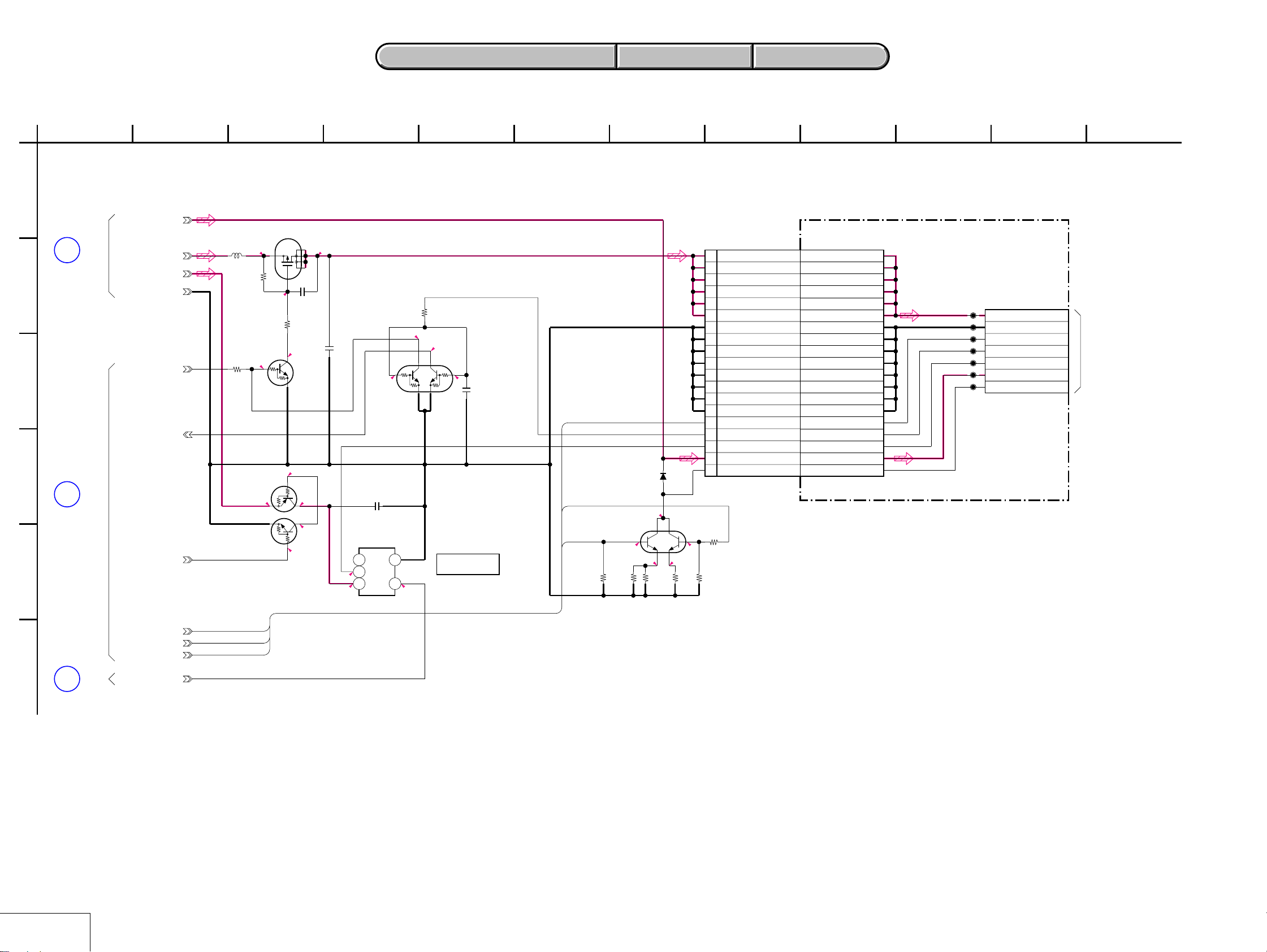
DSC-T1
• NOTE FOR REPAIR
SELF-DIAGNOSIS FUNCTION
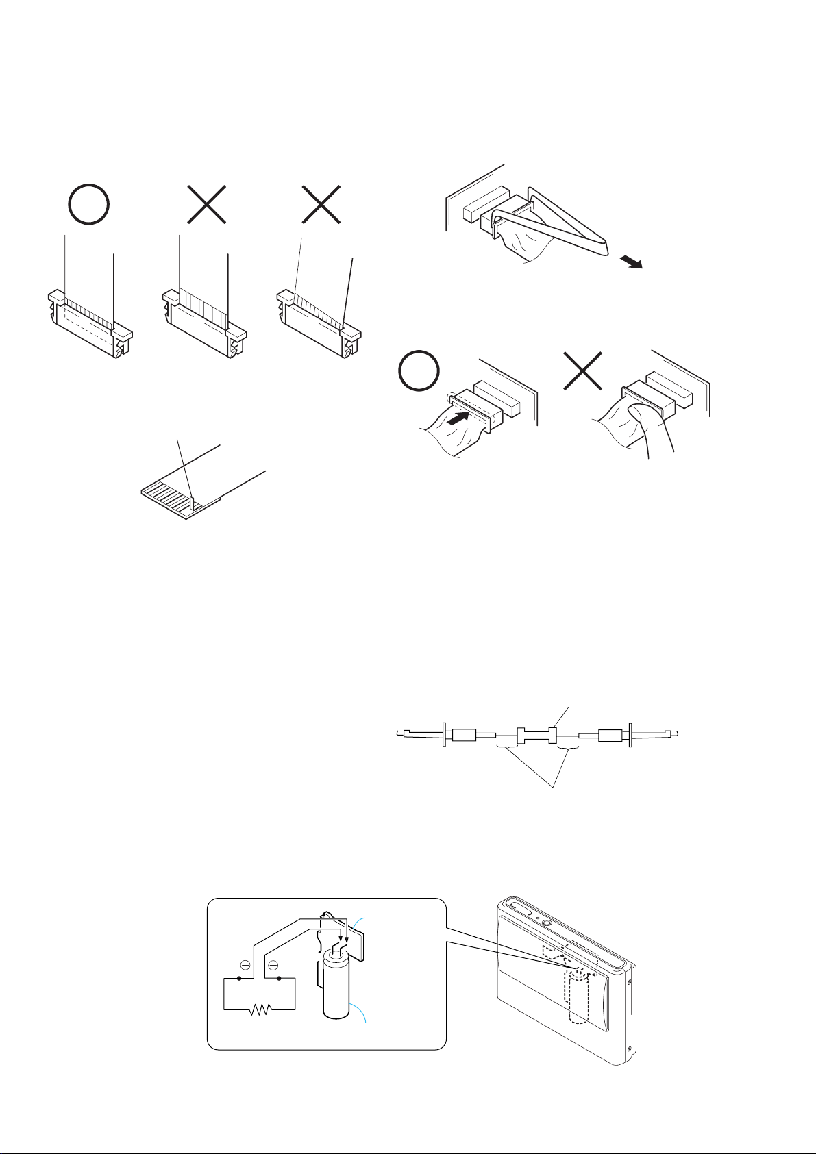
Make sure that the flat cable and flexible board are not cracked of
bent at the terminal.
Do not insert the cable insufficiently nor crookedly.
Cut and remove the part of gilt
which comes off at the point.
(Take care that there are
some pieces of gilt left inside)
When remove a connector, don't pull at wire of connector.
Be in danger of the snapping of a wire.
When installing a connector, don't press down at wire of connector.
Be in danger of the snapping of a wire.
[Discharging of the FLASH unit’s charging capacitor]
The charging capacitor of the FLASH unit is charged up to the
maximum 300 V potential.
There is a danger of electric shock by this high voltage when the
capacitor is handled by hand. The electric shock is caused by the
charged voltage which is kept without discharging when the main
power of the DSC-T1 is simply turned off. Therefore, the remaining
voltage must be discharged as described below.
Preparing the Short Jig
To preparing the short jig. a small clip is attached to each end of a
resistor of 1 kΩ /1 W (1-215-869-11)
Wrap insulating tape fully around the leads of the resistor to prevent
electrical shock.
Discharging the Capacitor
Short circuits between the positive and the negative terminals of
charged capacitor with the short jig about 10 seconds.
1 kΩ/1 W
Wrap insulating tape.
ST-86 B0ARD
Shorting jig
(1kΩ / 1w)
Capacitor
— 4 —
Page 3

[Description on Self-diagnosis Display]
Self-diagnosis display
• C: ss: ss
The contents which can be handled
by customer, are displayed.
• E: ss: ss
The contents which can be handled
by engineer, are displayed.
DSC-T1
Display Code
C:32:01
C:13:01
E:91:01
E:61:00 *1
E61:10 *1
Note : The error code is cleared if the battery is removed, except defective flash unit.
*1: The error display is given in two ways.
Turn off the main power then back on.
Replace the memory stick.
Format the memory stick with the DSC-T1.
Checking of flash unit or replacement of
flash unit.
Checking of lens drive circuit
Countermeasure
Trouble with hardware.
• The type of memory stick that cannot be
used by this machine, is inserted.
• Data is damaged.
• Unformatted memory stick is inserted.
Abnormality when flash is being
charged.
When failed in the focus initialization.
Cause
Caution Display During Error
SYSTEM ERROR
MS ERROR
Flash LED
Flash display
Flashing at 3.2 Hz
—
— 5 —
Page 4
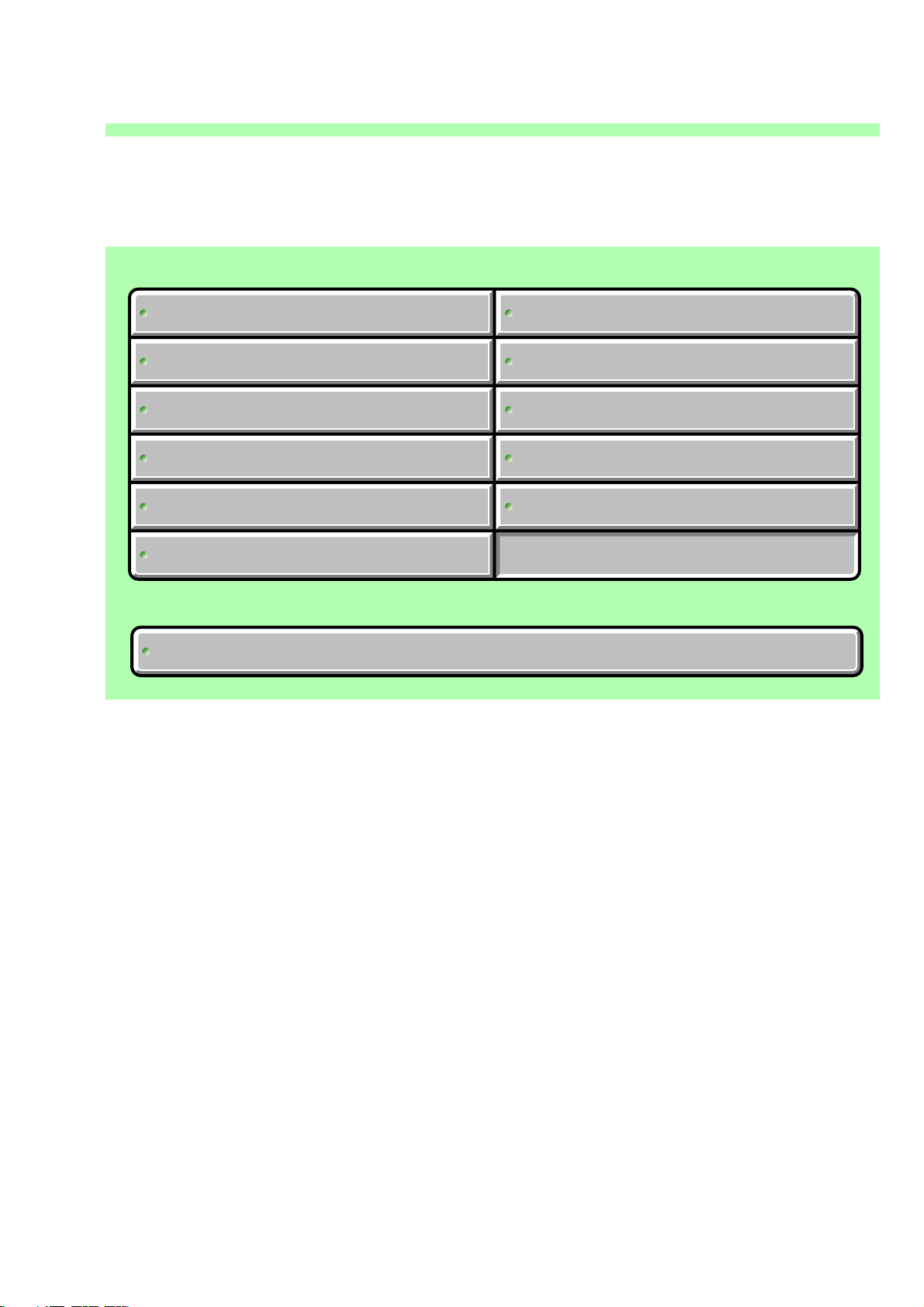
4-2. SCHEMATIC DIAGRAMS
COMMON NOTE FOR SCHEMATIC DIAGRAMS
COMMON NOTE FOR SCHEMATIC DIAGRAMS
Link
Link
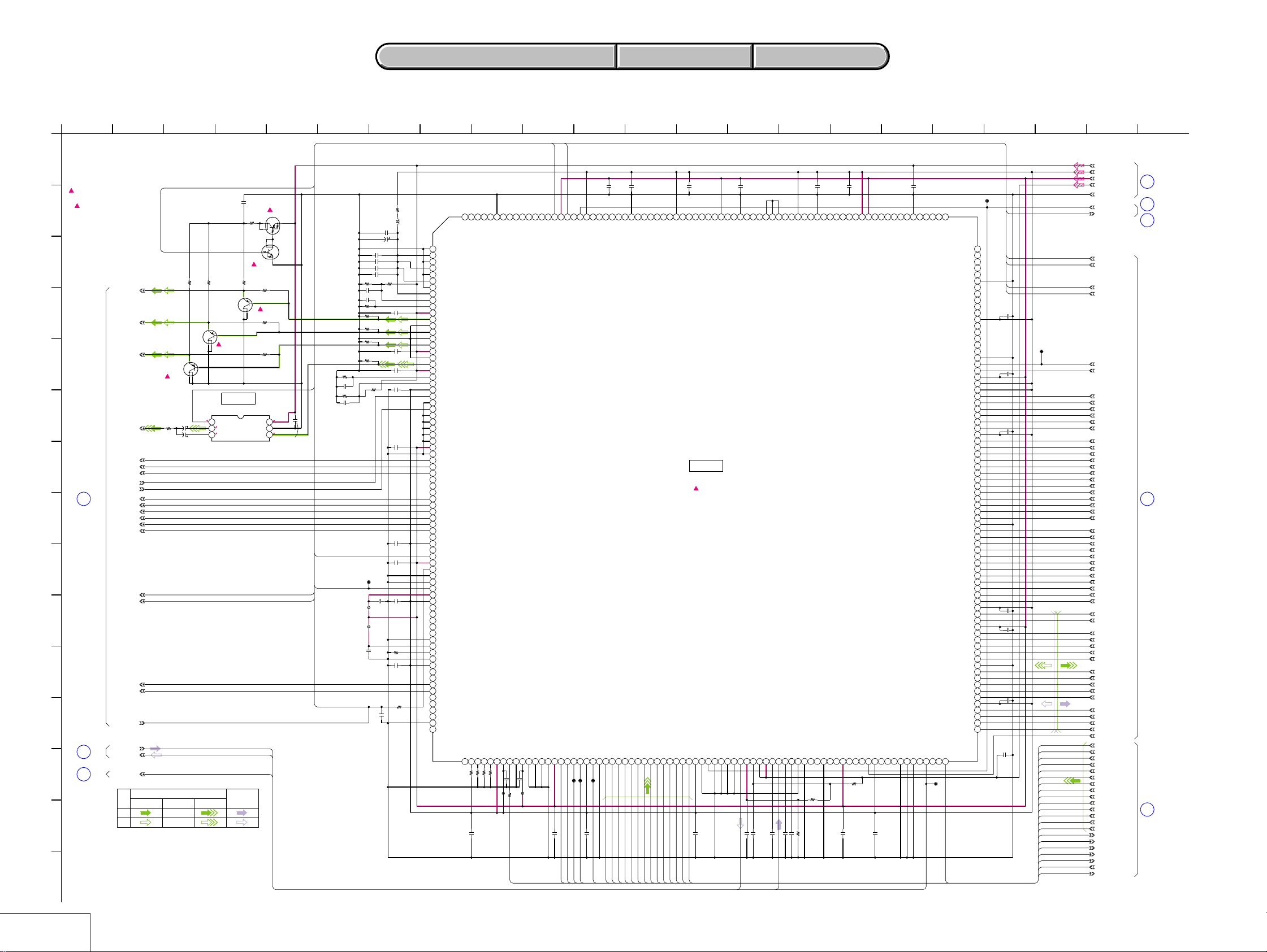
SY-95 BOARD (1/8)
SY-95 BOARD (1/8)
(CAMERA A/D CONVERTER, TIMING GENERATOR)
(CAMERA A/D CONVERTER, TIMING GENERATOR)
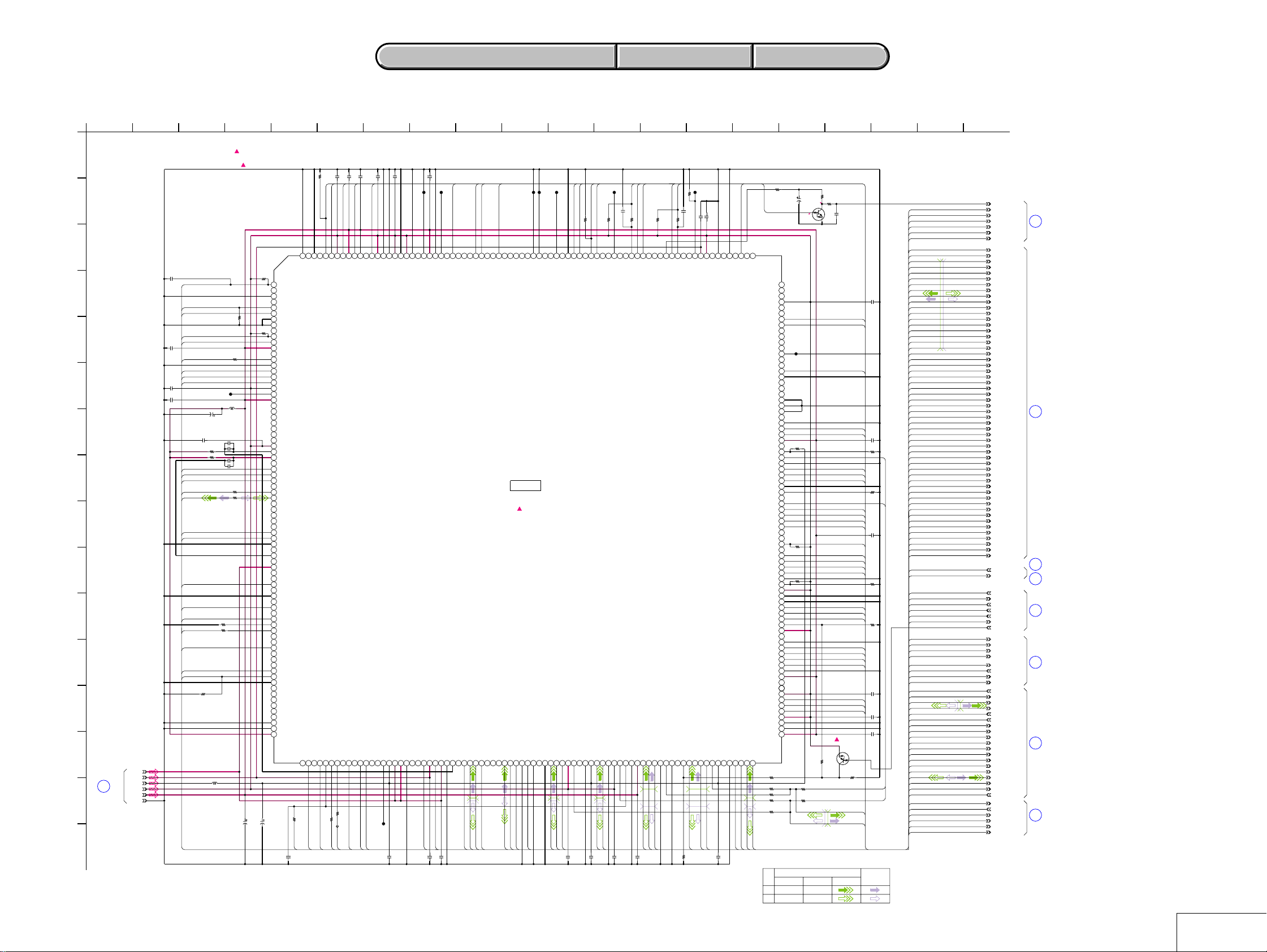
SY-95 BOARD (2/8)
SY-95 BOARD (2/8)
(CAMERA DSP, LENS CONTROL)
(CAMERA DSP, LENS CONTROL)
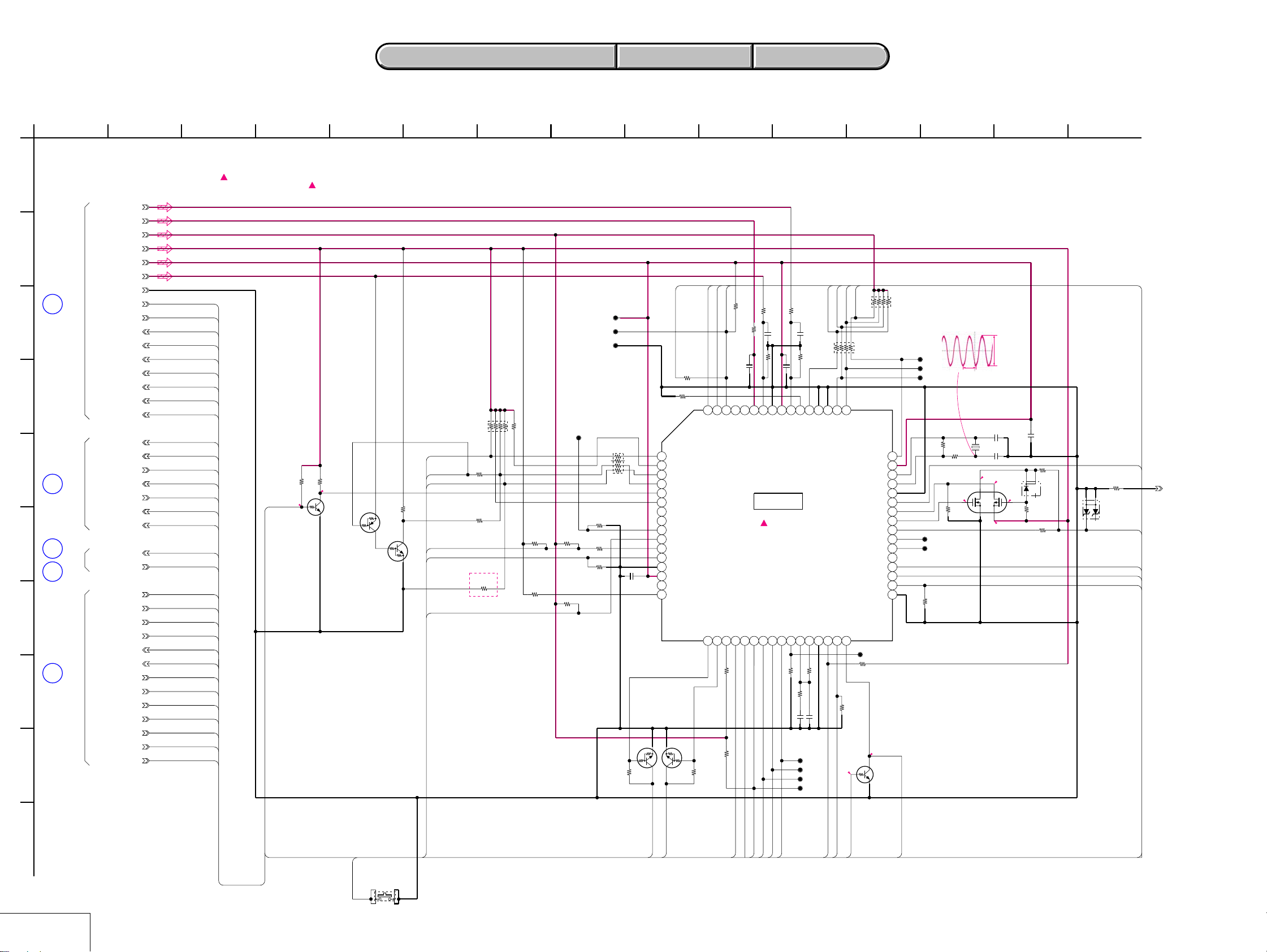
SY-95 BOARD (3/8)
SY-95 BOARD (3/8)
(CAMERA SYSTEM CONTROL)
(CAMERA SYSTEM CONTROL)
SY-95 BOARD (7/8)
SY-95 BOARD (7/8)
SY-95 BOARD (8/8)
SY-95 BOARD (8/8)
MS-148 BOARD (1/2)
MS-148 BOARD (1/2)
(DC/DC CONVERTER)
(DC/DC CONVERTER)
(CONNECTOR)
(CONNECTOR)
(MS I/O)
(MS I/O)
DSC-T1
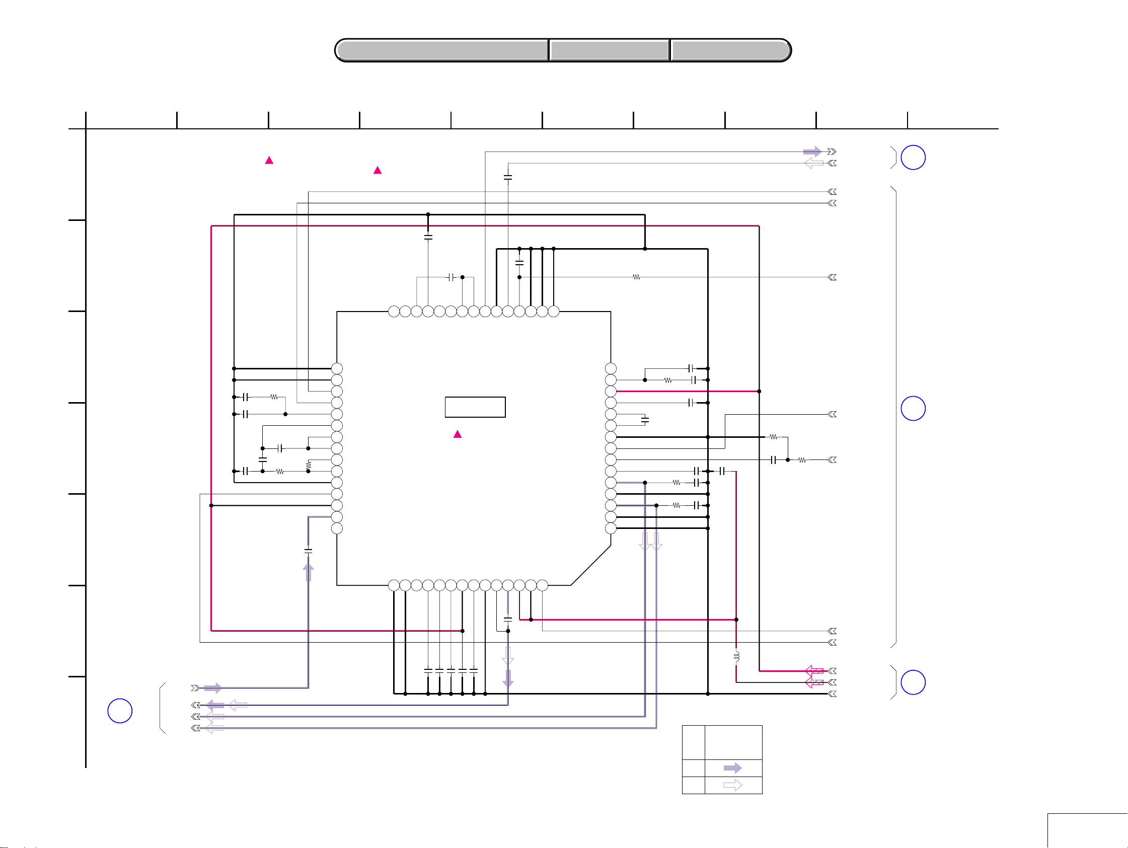
SY-95 BOARD (4/8)
SY-95 BOARD (4/8)
SY-95 BOARD (5/8)
SY-95 BOARD (5/8)
SY-95 BOARD (6/8)
SY-95 BOARD (6/8)
(HI CONTROL)
(HI CONTROL)
(AUDIO I/O)
(AUDIO I/O)
(FLASH DRIVE)
(FLASH DRIVE)
MS-148 BOARD (2/2)
MS-148 BOARD (2/2)
LD-140 BOARD
LD-140 BOARD
(LENS DRIVE)
(LENS DRIVE)
(LCD PANEL DRIVE)
(LCD PANEL DRIVE)
Page 5
DSC-T1
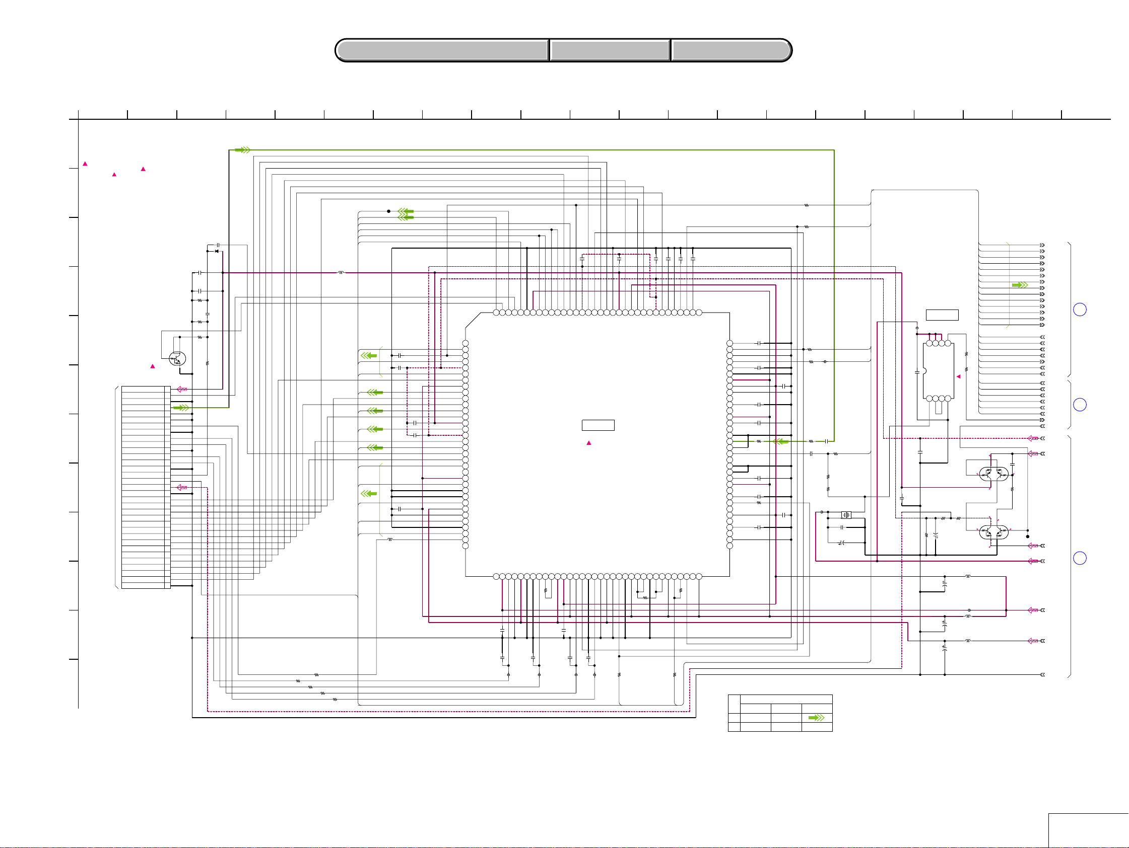
4-2. SCHEMATIC DIAGRAMS
1
SY-95 BOARD(1/8)
CAMERA A/D CONVERTER,TIMING GENERATOR(BLOCK)
A
XX MARK:NO MOUNT
NO MARK:REC/PB MODE
:Voltage measurement of the CSP IC
and the Transistors with mark and
the IC with mark ,is not possible.
B
C151
0.22u
C
D
E
F
G
H
I
J
K
L
TO
CD-463 BOARD
(PAGE 4-7
of LEVEL2)
16
Q153
UNRL21300AS0
SWITCH
1
33PCN702
33CAM_15V_CD
32POWER_SAVE
31REG_GND
30CCD-OUT
29REG_GND
28REG_GND
27RG
26REG_GND
25H2B
24H2A
23REG_GND
22H1B
21H1A
20REG_GND
19SHT
18VSUB_CONT
17CAM_-8.0V_CD
16REG_GND
15V1A
14V1B
13V2
12V3A
11V3B
10VST
9V4
8V5A
7V5B
6VHLD
5V6
4V7A
3V7B
2V8
1REG_GND
D151
MA2S111-(K8).SO
C153
4.7u
C190
4.7u
R152
1M
34
2
B
1
2
R151
100k
C152
0.22u
B
2012
R160
100k
R153
0
4-2. SCHEMATIC DIAGRAMS
4-2. SCHEMATIC DIAGRAMS
For Schematic Diagram
• Refer to page 4-47 for printed wiring board.
CL151
D0
D1
XTG_CS
CAM_SO
XCAM_SCK
XFE_CS
L151
100uH
±10%
D2
C155
0.01u
B
D3
C156
0.1u
B
D4
D5
D6
C157
0.01u
D7
D8
D9
D10
D11
D12
D13
VSUB_CONT
R155
10
R156
10
10
R157
10R158
10
R159
B
C158
0.1u
B
C159
0.1u
B
L155
10nH
SY-95 BOARD SIDE A SY-95 BOARD SIDE B
SY-95 BOARD SIDE A SY-95 BOARD SIDE B
124
125V6126
SEN
TSDATA
CSP(CHIP SIZE PACKAGE)IC
XX
B
11
C160
0.1u
B
118
119
120
121V8122VL123
V7A
SDL
TRESET
IC151
CAMERA A/D CONVERTER,
TIMING GENERATOR
IC151
CXD3433GA-T4
C189
XX
B
FB158
FB159
0uH
0uH
9
127
128
129
130
131
132
133
134D0135
136
D1
ID/EXP
TSEN
WEN/FLD
NC
1
D2
2
3
RST
D3
4
VMM
5
D4
6
Vhld
7
VDD4
8
D5
9
V1A
10
Vst
11
D6
12
V1B
13
VHH
14
D7
15
VLL
16
V3A
17
D8
18
SUB
19
V3B
20
D9
21
DLLSL
22
AVD1
23
D10
24
SNCSL
25
SSGSL
26
D11
27
AVD2
28
TEST1
29
D12
30
VSS1
31
D13
32
RG
33
NC
34
NC36DRVDD37H1A38DRVSS39AVD340DVSS141VSS242H1B43ADCCK44ADCLKT45AVD446DVDD147VDD148H2A49HD50VSS351H2B52VSS53AVD554VSS555CLPOBIt56VSS457AVD658SHPt59XSHPT60VSS661SHDt62XSHDT63VDD264CLPDMIt65CLPDMT66VD67P4968AVD7
35
C177
0.1u
B
C186
C187
XX
B
FB156
0uH
SSI
SCK
VSS9
AVD9
TSCLK
R167
100
C178
0.1u
B
XX
B
C188
FB157
0uH
12
R161
0
R162
220
C161
0.01u
B
116VH117
V7B
AVSS3
R172
C162
0.1u
B
113V2114
115
V5A
V5B
VDDA2
R183
XX
220
C165
C163
C164
0.1u
1u
1u
B
B
B
103NC104CM105HR106
107
108
109V4110VM111NC112
REFP
REFN
TRST
LME
VR
AVSS2
MCKO
LMO
VSS8
AVD8
VDDA1
OSCI
CKO
LP2E
OSCO
VDD3
LP2O
PBLK
VSS7
CCDIN
TEST3
CKI
NC
TEST2
AVSA/B
L
AVDA/B
P38
LP1E
CLPOB
P50
VDDD
P6
LP1O
DLLRST
AVSS1
NC
R184
XX
R173
220
C166
120p
CH
102
101
100
99
98
97
96
95
94
93
92
91
90
89
88
87
86
85
84
83
82
81
80
79
78
77
76
75
74
73
72
71
70
69
CH
120pC167
C169
18p
CH
C170
18p
CH
R165
0
C173
1u
B
C174
0.47u
B
R181
XX
C176
0.47u
B
R163
220
R164
FB151
100
C168
0.1u
B
R166
100
C172
0.01u
B
C175
0.1u
B
FB153
0uH
XCAM_RST
CA_HD
CAM_F
0uH
C171
0.1u
B
MCKG
R185
XX
TG_CLK
R186
0
R187
0
X151
54MHz
3
4
1
2
C192
0.1u
B
C194
22u
6.3V
1825 15 16
IC152
CLOCK GEN.
FB160
0uH
5Q6
7
8
xPR
VCC
xCLR
C193
0.1u
B
GND
1CK2D3xQ4
C191
1u
B
RN2907FE(TPLR3)
C180
4.7u
16V
B
R178
0
C181
R179
22u
100k
16V
TA
B
C183
100u
6.3V
C184
100u
6.3V
C185
100u
6.3V
IC152
TC7WH74FK(TE85R)
Q151
SWITCH
R177
0
Q152
RN1907FE(TPLR3)
SWITCH
L152
10uH
±20%
FB152
0uH
L153
10uH
±20%
L154
10uH
±20%
19144 1763
D0
D1
D2
D3
D4
D5
D6
D7
D8
D9
D10
D11
D12
D13
CA_HD
CAM_F
CL_POB
R190
CLP_DM
0
MCKTG
TG_CLK
R191
220
VSUB_CONT
CAM_F
CAM_SO
XCAM_SCK
XFE_CS
XTG_CS
XCAM_RST
15.0
4
1
3.7
5
3
6
14.9
-7.9
0.1
6
3
5
1
4
-8.0
20810 13 217
CA_AD00
CA_AD01
CA_AD02
CA_AD03
CA_AD04
CA_AD05
CA_AD06
CA_AD07
CA_AD08
CA_AD09
CA_AD10
CA_AD11
CA_AD12
CA_AD13
CA_HD
CAM_F
CLP_OB
CLP_DM
MCKTG
TG_CLK
VSUB_CONT
CAM_F
CAM_SO
XCAM_SCK
XFE_CS
XTG_CS
XCAM_RST
VER_EXT_CLK
CAM_DD_ON
CAM_-0.5V
CAM_15.0V
C179
0.1u
B
2.7
2
R174
82k
2.83.6
2
CL152
CAM_-8.0V
D_2.8V
A_2.8V
A_3.1V
REG_GND
(2/8)
1
(3/8)
2
(7/8)
3
SIGNAL PATH
CLPOB
CLPDM
REC
PB
CHROMA
VIDEO SIGNAL
Y/CHROMAY
4-15 4-16
SY-95 (1/8)
Page 6
DSC-T1
For Schematic Diagram
• Refer to page 4-47 for printed wiring board.
1
SY-95 BOARD(2/8)
CAMERA DSP,LENS CONTROL(KIW BLOCK)
A
XX MARK:NO MOUNT
NO MARK:REC/PB MODE
( ) MARK:WHEN CONNECTED CRADLE and TV MONITOR.
:Voltage measurement of
the CSP IC and
the Transistors with
mark,is not possible.
B
AMP_OUT_ON
C
R310
R311
2200
Q302
EC3101C-PM-TL
R305
68
VIDEO SIGNAL
2200
2
1
4
3
EC3101C-PM-TL
2
1
4
3
0(2.8)
C322
100u
1
4V
C332
22u
6.3V
TA
Power Save
0.3(0.9)
2
Vout
0.3(0.9)
3
Vsag
P
Y/CHROMA
PANEL_G
D
PANEL_B
PANEL_R
E
F
V_OUT
HR_EN0
G
4
H
HR_DIR0A
HR_DIR0B
XZM_RST_SENS1
XFC_RST_SENS
(8/8)
HR_EN2
HR_DIR2A
HR_DIR2B
HR_EN3
HR_DIR3A
HR_DIR3B
I
PANEL_V
HD0
J
K
XZM_RST_LED
XFC_RST_LED
L
5
6
M
XRST_SYS
AU_AOUT
(5/8)
AU_AIN
STRB_ON
(6/8)
REC
N
PB
O
16
Q303
IC302
R312
2200
VIDEO AMP
AUDIO
SIGNALYCHROMA
3
NJM2578KJ1(TE3)IC302
2
C359
XX
R352
0
UNRL21300AS0
R304
Q302-304
BUFFER
1
4
R302
R303
GND
AU_AOUT
STRB_ON
Q305,306
SWITCH
UNRL11400AS0
3
4
4
1
Q305
XX
Q304
EC3101C-PM-TL
XX
XX
VIDEO_AMP_ON
Vcc
Vin
AU_AIN
AMP_OUT_ON
Q306
1
3
2
2.8
6
5
0(0.2)
4
4-2. SCHEMATIC DIAGRAMS
4-2. SCHEMATIC DIAGRAMS
VDDI_8
OPBCLP
HD0
CLP_DM
HD
DUMCLP
CL302
CA_HD
(NC)LCDCK
CCDHD
CL303
CAM_F
NTVDO
CCDFD
VDDE_15
VDDE_5
XXC328
11
(NC)DQ16
CLKTGI
AC16AC15AA17
CL304
MCKTG
9
Note:Resistor is mounted to the location FB306 is printed.
FB306
0
Note
L301
2
C302
C306
C307
R331
±0.5%
C308
0.1u
C360
4700p
10kR332
±0.5%
560R324
±0.5%
±0.5%
R326
560
±0.5%
R315 150
±0.5%
R316
2700
±0.5%
C361
0.022u
R317
±0.5%
C305
0.1u
C304
10u
B
PLLBYPASS
MC_CKIO
PANEL_V
HD0
XRST_SYS
R319 27k
±0.5%
18k
FB302
0uH
FB303
0uH
C315
10u
47uH
C362
4.7u
C357
4V
100u
1u
1uC303
0.1u
1u
18k
R334
27k
±0.5%
C310
XX
560R325
C311
0.1u
C317
0.1u
C318
0.1u
C319
XX
C312
0.1u
XXC313
CL301
C320
C314
10u
XX
R327
0
C316
XX
R318
C309
1k
0.1u
SDRAM_VSS0
A1
SDRAM_VDD0
A2
SDRAM_VSS1
M1
SDRAM_VDD1
N1
SDRAM_VSSQ0
A23
SDRAM_VDDQ0
A22
SDRAM_VSSQ1
M23
SDRAM_VDDQ1
N23
VREF1
B23E22D21C23E20D23F22E23G22E21F23H22G23H23J23F20G20F21H20J22G21H21J20K23K22K20L22J21R23T23U23V23U20R22R21V20T21W23Y23
VR01
VAVD0
G0
VAVS0
B0
VAVS1
R0
VAVD1
VAVS2
Y0
VAVD2
VR02
VREF2
VDDE_0
SENS0
SENS1
SENS2
SENS3
FG0A
FG0B
FG1A
FG1B
VDDI_0
GND_0
EN0
DIROA
DIROB
EN1(NC)
DIR1A(NC)
DIR1B(NC)
EN2
DIR2A
DIR2B
EN3
DIR3A
L21P22 N21T20 N20P23 M20R20 M21N22 L20L23 K21P20 M22P21
DIR3B
IRIS_COM(NC)
VDDE_1
PLLCKOUT(NC)
XRSTMON
VDDI_1
RSTX
GND_1
PLLGND1
CLKI
PLLVDI1
VDDE_2
PIO14(NC)
PIO13(NC)
PIO12(NC)
PIO11(NC)
PIO10(NC)
GND_2
PLLVDI2
CLKTGEXT
AA23AB23AC23
PLLGND2
VDDE_3
PIO09(NC)
U21T22V21U22V22W20W22Y20
PIO08(NC)
PIO07
PIO06
PIO05(NC)
PIO04(NC)
PIO03(NC)
PIO02(NC)
GND_3
AC22
PIO01(NC)
W21
Y22 Y21
C321
0.1u
GND_16
(NC)F_D1
(NC)F_D0
(NC)FCK27
PLLMD2
(NC)VOEN
PLLMD3
VDDE_4
C323
FB304
(NC)F_D2
CLKTGO
PLLGNDTG
PLLVDETG
10u
10u
C324
XX
0uH
R307
TG_CLK
(NC)F_VD
(NC)F_HD
(NC)F_FLD
PLLMD1
PIO00(NC)
PLLMD0
AA22
AB22AA21AB21 AC21AC20AB20 AC19AA20 AA19 Y19 AB19AC18 Y18 AA18 Y17AB18 AC17
0
R3530R3540R3550R356
PANEL_V
LCDVD
(NC)F_D4
(NC)F_D6
(NC)F_D3
(NC)F_D5
(NC)F_D7
MD0
VDDI_2
PLLVDITG
MD2
GND_4
MD1
0uH
FB305
XX
C326
CLP_OB
SY-95 BOARD SIDE A SY-95 BOARD SIDE B
SY-95 BOARD SIDE A SY-95 BOARD SIDE B
C330
0.1u
VDDE_14
(NC)DQ27
(NC)DQ26
CAMERA DSP, LENS CONTROL
CSP(CHIP SIZE PACKAGE)IC
ADIN04
ADIN03
ADIN02
CA_AD01
CA_AD02
CA_AD03
(NC)DQ29
(NC)DQ28
IC301
(KI(5M SA)BOARD)
ADIN00
ADIN01
XX
C331
CA_AD00
13
(NC)DQ30
VDDE_6
(NC)DQ31
IC301
CKADI
(NC)DQM0
NTVDI
(NC)DQM1
PLLGND3
VDDI_7
AUCKEXT
C334
XX
(NC)DQM2
PLLVDI3
(NC)DQM3
AVS_2
AU_AIN
GND_14
AOUT
C343
0.1u
A10B10
C10
D10D11C11A11B11D12A12D13B12C12A13B13C13A14B14C14A15D14B15C15A16B16D15B17C16A17B18A18D16C17C18A19D17B19C19D18A20B20C20D19B21A21C21B22D20C22D22
XCS0
VDDE_13
(NC)XCASVR
(NC)XRAS
(NC)QCLKE
SDRAM_CS0
SDRAM_CS1
AVS_1
AIN
VRL
AVDD_1
VRH
TRST
AC9 AB9 AC8 Y9 AA10 Y8 AA9 AB8 Y7 AA8 AC7 AC6 Y6 AB7 AA7 AC5 AC4 AC3 AA6
±0.5%
±0.5%
0.1u
0.1u
0.1u
10k
C341
C340
C342
R344
AU_AOUT
0.1u
C335
(NC)XCS3
VRN
0.1u
C336
(NC)XCS2
VRP
(CN)XCS1
AVDD_2
12
C327
C329
0.1u
XX
GND_15
(NC)DQ25
(NC)DQ20
ADIN11
CA_AD10
(NC)DQ21
ADIN10
CA_AD09
ADIN09
CA_AD08
(NC)DQ22
ADIN08
CA_AD07
(NC)DQ23
ADIN07
CA_AD06
(NC)DQ24
ADIN06
CA_AD05
ADIN05
CA_AD04
(NC)DQ19
(NC)DQ18
(NC)DQ17
ADIN13
GND_5
ADIN12
AA16AB16 Y16 AA15AA14AB15 Y15 AB14AA13 Y14 AB13 Y13AC14 Y12AA12AB12 Y11AC13 AB11AC12 AC11AC10 Y10AA11 AB10
AB17
CA_AD11
CA_AD12
CA_AD13
R345
5600
(NC)QCLK
TMS(NC)
GND_13
TCK(NC)
(NC)XWE
GND_6
(NC)AQ00
TDI(NC)
C345
0.1u
C346
0.1u
(NC)AQ01
TDO(NC)
(NC)AQ02
VDDI_3
(NC)AQ03
AUCK64(NC)
R346
10k
±0.5%
(NC)AQ04
XPWAD(NC)
VDDE_12
XPWDA(NC)
C348
XX
VDDI_6
AUCK
(NC)AQ05
VDDE_7
(NC)AQ07
(NC)AQ08
(NC)AQ09
(NC)AQ06
SOA(NC)
ADCK(NC)
SIA
SCLK(NC)
Y5 AB6 AB5 AA5 AB4 AB3 AA4 AC2
(NC)AQ10
GND_7
GND_12
APBD
C358
XX
(NC)AQ11
SHUTTER(NC)
STRB_ON
(NC)AQ12
STROBE1
CL305
(NC)BA1
(NC)BA0
STROBE3(NC)
STROBE2(NC)
A3C3B4A4B5A5B6B7C4D4C7D5A6A7C5D6C6D7D8D9A8B8C8A9B9C9
(NC)DQ00
SUBCNTL(NC)
VSUB_CONT
182 225 15 16
(NC)DQ01
(NC)DQ02
(NC)DQ03
(NC)DQ04
(NC)DQ05
(NC)DQ06
(NC)DQ07
(NC)DQ08
(NC)DQ09
(NC)DQ10
VDDE_11
(NC)DQ11
(NC)DQ12
(NC)DQ13
(NC)DQ14
(NC)DQ15
XWAITIN2
XWAITIN1
CSXRAM
RD_XWR
VDDE_10
GND_11
GND_10
VDDI_5
VDDE_9
VDDI_4
VDDE_8
XWAIT
WRHX
WRLX
GND_9
GND_8
XRST_SYS
AMP_OUT_ON
VIDEO_AMP_ON
PLLBYPASS
MC_CKIO
CL311
CA_AD00
CA_AD01
CA_AD02
CA_AD03
CA_AD04
CA_AD05
CA_AD06
CA_AD07
CA_AD08
CA_AD09
CA_AD10
CA_AD11
CA_AD12
CA_AD13
TG_CLK
CLP_OB
CLP_DM
CA_HD
CAM_F
MCKTG
VSUB_CONT
20810
19144 1763
CL310
C349
XX
C350
IRQ
CSX
BSX
A1
A2
A3
A4
A5
A6
A7
A8
A9
A10
A11
A12
A13
A14
A15
A16
A17
A18
A19
A20
A21
A22
A23
A24
A25
D0
D1
D2
D3
D4
D5
D6
D7
D8
D9
D10
D11
D12
D13
D14
D15
XX
C351
1u
C352
1u
C353
XX
Y2 Y4 Y1 W4 W2 V4 W1 V2 V1 V3 U4 U1 U3 U2 T4 T2 R4 T1 T3 R2 R3 R1 P3 P4 P1 N4 P2 N3 N2 M3 M4 M2 L3 K3 L1 L4 L2 J3 K1 K4 J4 K2 H3 J1 J2 H4 G3 H1 H2 G4 G1 G2 F3 F1 F4 F2 E1 E3 E2 E4 D2 D3 D1 C2C1B2B1B3
AA1
W3
C354
0.1u
AB2 AC1 AA3 Y3 AB1 AA2
C337
0.1u
217
A_2.8V
D_2.8V
D_1.2V
AU_2.8V
REG_GND
SYS_V
XRST_SYS
AMP_OUT_ON
VIDEO_AMP_ON
PLLBYPASS
MC_CKIO
MC_XWAIT
IRQ_IMG
MC_XCS_IC301SDRAM
MC_XCS_IC301REG
MC_XBS
MC_XWE1
MC_XWE0
MC_RDXWR
MC_A1
MC_A2
MC_A3
MC_A4
MC_A5
MC_A6
MC_A7
MC_A8
MC_A9
MC_A10
MC_A11
MC_A12
MC_A13
MC_A14
MC_A15
MC_A16
MC_A17
MC_A18
MC_A19
MC_A20
MC_A21
MC_A22
MC_A23
MC_A24
MC_A25
MC_D0
MC_D1
MC_D2
MC_D3
MC_D4
MC_D5
MC_D6
MC_D7
MC_D8
MC_D9
MC_D10
MC_D11
MC_D12
MC_D13
MC_D14
MC_D15
AU_LRCK
CA_AD00
CA_AD01
CA_AD02
CA_AD03
CA_AD04
CA_AD05
CA_AD06
CA_AD07
CA_AD08
CA_AD09
CA_AD10
CA_AD11
CA_AD12
CA_AD13
TG_CLK
CLP_OB
CLP_DM
CA_HD
CAM_F
MCKTG
VSUB_CONT
(7/8)
7
(3/8)
8
(4/8)
8
(3/8)
9
(1/8)
1
SY-95 (2/8)
4-17 4-18
Page 7
DSC-T1
For Schematic Diagram
• Refer to page 4-47 for printed wiring board.
1
L501
C509
22u
4V
R503
100
C503
XX
100R504
C504
XX
R543
R515
22
10uH
NO MARK:REC/PB MODE
:Voltage measurement of
the CSP IC and
the Transistors with
mark,is not possible.
R566
XX
R510
22
CL512
L502
10uH
C512
B
10u
C513
10u
B
22
R512
R513
22
0
C502
22u
4V
SY-95 BOARD(3/8)
CAMERA SYSTEM CONTROL(EVR BLOCK)
A
XX MARK:NO MOUNT
B
C
D
E
F
G
H
I
J
K
L
M
N
A_2.8V
D_1.8V
A_3.1V
(7/8)
10
D_2.8V
D_1.2V
O
REG_GND
P
16
C505
C506
C507
0.1u
B
XX
XX
C510
XX
LENS_TEMP
VER_EXT_CLK
MC_CKIO
SYS_SI
CAM_SO
MC_MSD2
MC_XCS_IC301REG
MC_XCS_FLASH
MC_XWE0
C511
XX
SYS_SO
XCAM_SCK
FR_SI
MC_MSBS
MC_MSDIO
MC_XBS
XAU_HGL_SEL
AU_LRCK
XSYS_SCK
XFR_SCK
MC_MSD1
MC_XCS_IC301SDRAM
XACCESS_LED
XCAM_RST
R518
100k
4-2. SCHEMATIC DIAGRAMS
4-2. SCHEMATIC DIAGRAMS
11
CL504
CL509
XBEEP_MUTE
XAU_SP_MUTE
XAU_POWER_SAVE
47k
MC_JTAG_RTCK
R565
TMS
(NC)
(NC)TRACEPKT3
(NC)TRACEPKT4
AVRB(DA)
D9
H21 H22 H23 H24
MC_D9
MC_D4
RTCK
(NC)PIPESTAT2
D4
D17
SELF_TIMER_LED
C534
XX
VSS
PT[4]
(XAU_POWER_SAVE)
VMH
VDDQ
J1 J2 J3 J4
PT[6]
(NC)RTS5/SCK5
(XBEEP_MUTE)
ADGND(PHY)
ANOUT[3](NC)
PT[0]
(XAU_SP_MUTE)
AVDD1(PHY)_33
J21 J22 J23 J24
C533
TDO
VSS_F
(NC)RxD4
AVSS(DA2)
CAM_DD_ON
PU[6]
AVSS(PLL2)
(NC)PU[2]
D27(NC)
AMP_OUT_ON
(NC)PQ[4]
(NC)SCL(O/D)
D14
D19
MC_D14
XTG_CS
MC_D7
9
PQ[2]
D7
SP_VOL
XSTRB_FULL
TI2B
(SP_VOL)
ANOUT[2]
(NC)TO2
(NC)INT8
DACK3(NC)
ANOUT[1](NC)
CAM_F
INT2
AVSS(PLL3)(NC)
(NC)PIPESTAT1
(NC)TRACEPKT5
(NC)TRACEPKT2
(NC)TRACEPKT7
(NC)TRACEPKT0
IC501
CAMERA SYSTEM CONTROL
IC501
JSCIS001BF00GA-T6
CSP(CHIP SIZE PACKAGE)IC
D23
VSS
D12
D21
CK_F
G21 G22 G23 G24
H1 H2 H3 H4
PLLBYPASS
MC_CKIO
MC_D12
BL_MODE
CL503
7
C521
C519
C518
R507
XX
XX
100k
STRB_CHG
VSS
PU[0]
R508
47k
R511
100k
C501
22u
6.3V
TEST2
(NC)PU[4]
(NC)RTS4/SCK4
AN[5]
A2A3A4A5A6A7A8A9A10A11A12A13A14A15A16A17A18A19A20A21A22A23B1B2B3B4B5B6B7B8B9
AN[1](NC)
AVSS(AD)
XTAL(NC)
EXTAL
CKIO
VSSQ
VSS
TxD3(NC)
RxD2
TxD1
VDD
DREQ0(NC)
MSDATA2
VSSQ
CS5A
CS0
WE0/DQMLL
VDDQ
RD
VDD
D30(NC)
AN[11](NC)
AN[9](NC)
AN[3](NC)
AD/EXT(NC)
TEND(NC)
DREQ3(NC)
VDDQ
AVDD(PLL2)_12
AVDD(PLL1)_12
SCK3(NC)
B10B11B12B13B14
TxD2
SCK1
TxD0
DREQ1(NC)
MSBS
MSDATA0/MSDIO
B16B24 B15B23
CS6(NC)
B17
CS3(NC)
B18
WE2/DQMUL/ICIORD(NC)
B19
RAS(NC)
B20
A0(NC)
B21
BS
B22
D20
(XAU_HGL_SEL)
VSSQ
AN[7](NC)
C1
AVSS(PLL1)
C2
AN[2](NC)
C3
AVDD(AD)_30
C4
AN[0](NC)
C5
DACK2(NC)
C6
TCLK
C7C8C9
DREQ2(NC)
MD1
RxD3(NC)
C10C11C12C13C14C15C16C17C18C19C20C21C22C23C24
SCK2
RxD1(NC)
MSDIR
MSDATA1
CS5B(NC)
CS7/CE1(NC)
CS4
WE3/DQMUU/AH/ICIOWR(NC)
CAS(NC)
D26(NC)
D24
D22
VSSQ
AN[6](NC)
D1D2D3D4D5D6D7D8D9
ADRWCLK(NC)
AN[10](NC)
END(NC)
AN[8](NC)
AN[4](NC)
MD2
MD0
AVDD(PLL3)_12
DACK1(NC)
RxD0
DACK0(NC)
RST
SCS0
D10 D11 D12 D13 D14 D15 D16D17 D18 D19 D20 D21D22 D23 D24
R522
R521
22
1k
FR_SO
XSYS_RST
XCS_MC
C523
0.1u
MS_PWR_ON
SDA(O/D)
MSDATA3
MC_MSD3
VDDQ
MSSCLK
R548
15
FB523
0uH
MC_MSCLK
XPANEL_TG_CS
PQ[0]
CS2(NC)
MC_XWE1
C520
0.1u
MELODY
TO0
VDD
VDD
WE1/DQMLU/ICWE
CKE(NC)
RD/WR
MC_RDXWR
(NC)INT4
D18
VIDEO_AMP_ON
C522
XX
0.1u
FR_INT
INT0
VSSQ
VDDQ
RDY_F
D29(NC)
D31(NC)
E1 E2
CL507
CL502
VSS
ADVDD1(PHY)_33
TCK
VDD
VSSQ
VDDQ
VSSQUTMI
VDDQUTMI_30
(NC)PIPESTAT0
AVRT(DA)_30
C524
0.1u
VCC_F_18
D28(NC)
AVDD(DA2)_30
D25(NC)
AVSS(DA0)
D15
E3 E4 E21 E22 E23E24 F1 F2 F3 F4 F21F22 F23 F24 G1 G2 G3 G4
MC_D15
PRELAMP_AF_CONT
C530
C529
10u
B
0.1u
C527
XX
CL508
TEST1
ANOUT[0]
RxD5
AVDD(DA0)_30
SY-95 BOARD SIDE A SY-95 BOARD SIDE B
SY-95 BOARD SIDE A SY-95 BOARD SIDE B
12
CL510
MC_UPDATE
XXC556
XX
R562
TxD5
PT[2]
(NC)TI3A
(NC)PT[3]
(NC)PQ[6]
VMF
VIO_F_30
D5
VSSQ
D6
K1 K2 K3 K4
MC_D6
MC_D5
C535
0.1u
XX
R558
(NC)CTS4
XRESET_F
XSHTR_ON
1k
INT6
AGND1(PHY)
XCAM_DR_PS
XSTRB_PWR_ON
PU[5]
DVDD1(PHY)_12
K21 K22 K23 K24
MC_D8
C536
0.1u
13
100kR551
CL505
IRQ_IMG
XAE_LOCK_ON
XX
1u
XX
1k
XX
R559
C557
C538
C537
TO1
INT3
INT7
(NC)TO3
(NC)TRACECLK
(NC)TRACEPKT1
VSSIO_F
VBUSOTG0
VBUSCHG(NC)
VPH
DGND1(PHY)
D0
L21 L22 L23 L24 M1 M2 M3 M4 M21M22 M23 M24
L1 L2
L3 L4
MC_D0
R530
0
MC_JTAG_XTRST
TRST
D16(NC)
AB1AB2AB3AB4AB5AB6AB7AB8AB9
MD3
VDDQ
TEST0
MC_D13
(NC)PT[5]
(NC)STATUS0
SUSPENDN(NC) (NC)IOIS16
VSSUSBHS
AVDD31(PHY)_33
D13
A24
VPF
MC_A24
C539
0.1u
VCC_F_18
D1
MC_D1
R561
AB10AB11AB12AB13AB14AB15AB16AB17AB18AB19AB20AB21AB22AB23AB24AC1AC2AC3AC4AC5AC6AC7AC8AC9AC10AC11AC12AC13AC14AC15AC16AC17AC18AC19AC20AC21AC22AC23AC24AD2AD3AD4AD5AD6AD7AD8AD9AD10AD11AD12AD13AD14AD15AD16AD17AD18AD19AD20AD21AD22AD23
PU[1]
(NC)PQ[5]
(NC)PQ[1]
D11
D8
D3
MC_D11
MC_D3
XAU_LINE_MUTE
AA16AA17AA18AA19AA20AA21AA22AA23AA24
PT[1]
(NC)CTS5
AVDD(OTGCH0)_33
A15
D10
MC_A15
MC_D10
(NC)TRACESYNC
(NC)TRACEPKT6
VDDUSBOTG_12
MC_D2
R553
2700
MELODY
(NC)
(NC)TxD4
(NC)PU[7]
(NC)PU[3]
VDDQ
(NC)PQ[7]
INT5
PQ[3]
INT1
(NC)TI3B
(NC)TI2A
(NC)INT9
TDI
(NC)
(NC)
WAIT
MD4
(NC)CE2
(NC)STATUS1
VSSUSBOTG
(NC)CKIO2
VSS_F
A5
A7
VDD
(NC)
RPU
DMOTGCH0
VSSQ
A3
A1
A2
VSS
RREF
(NC)
DPOTGCH0
A21
A19
A6
A18
(NC)
(NC)
XCE_F
USBXTAL
A23
A25
A8
A16
AVSS(OTGCH0)
MD5
ACC_F
USBEXTAL
VSSQ
A9
A4
A14SCK0
VBUSHS
XWP_F
(NC)UCLK
VSSQUSB
A17
A13
A11
A12
HOLD
VDDUSB_12
(NC)VBUSEN
(NC)CIDOTG0
VDDQ
A22
A20
A10
VDDQUSB_30
VSSUSB
VBUSOTG1
VDDUSBHS_12
D2
R527
XX
R525 33
10
R528
33
10
R529
SIGNAL PATH
REC
PB
C552
3.3u
6.3V
P
AA10AA11AA12AA13 AA14AA15
CL506
Y21 Y22 Y23 Y24 AA1 AA2 AA3 AA4 AA5AA6 AA7 AA8 AA9
Y1 Y2 Y3 Y4
W21W22 W23W24
1.5k
±5%
R535
W1 W2 W3 W4
V21 V22 V23 V24
R550
U1 U2 U3 U4 U21U22 U23U24 V1 V2 V3 V4
XX
T21 T22 T23 T24
R557
XX
T1 T2 T3 T4
R21 R22 R23 R24
R1 R2 R3 R4
P21 P22 P23 P24
N1 N2 N3 N4 N21N22 N23N24 P1 P2 P3 P4
±0.5%
R533
±5%R531
XX
±0.5%
R532
XX
±5%
VIDEO SIGNAL
R554
10k
0
0
DTC144EMT2L
R536
0
YCHROMA Y/CHROMA
R555
4700
Q501
MOD.
C553
0.001u
VER_DMOTGCH0
VER_DPOTGCH0
MC_XCS_FLASH
Q502
DTA144EMT2L
VER_DPOTGCH0
VER_DMOTGCH0
B
INV.
USBPHY_D+
MC_XWAIT
R560
100k
USBPHY_D-
XFE_CS
MC_A21
MC_A19
MC_A18
MC_A23
MC_A25
MC_A16
MC_A14
MC_A17
MC_A13
MC_A11
MC_A12
MC_A22
MC_A20
MC_A10
1825 15 16
C540
XX
SYS_V
MC_A5
MC_A7
C543
XX
R552
XX
MC_A3
MC_A1
MC_A2
R538
510
±5%
MC_A6
C545
XX
MC_A8
R549
0
MC_A9
MC_A4
R539
XX
C546
XX
C547
0.1u
B
C548
0.1u
AUDIO
SIGNAL
XBEEP_MUTE
SP_VOL
XAU_HGL_SEL
XAU_POWER_SAVE
XAU_LINE_MUTE
XAU_SP_MUTE
VIDEO_AMP_ON
AMP_OUT_ON
MC_D0
MC_D1
MC_D2
MC_D3
MC_D4
MC_D5
MC_D6
MC_D7
MC_D8
MC_D9
MC_D10
MC_D11
MC_D12
MC_D13
MC_D14
MC_D15
MC_A1
MC_A2
MC_A3
MC_A4
MC_A5
MC_A6
MC_A7
MC_A8
MC_A9
MC_A10
MC_A11
MC_A12
MC_A13
MC_A14
MC_A15
MC_A16
MC_A17
MC_A18
MC_A19
MC_A20
MC_A21
MC_A22
MC_A23
MC_A24
MC_A25
MC_XBS
MC_RDXWR
MC_XWE0
MC_XWE1
MC_XWAIT
MC_XCS_IC301REG
MC_XCS_IC301SDRAM
MC_CKIO
AU_LRCK
IRQ_IMG
PLLBYPASS
XRST_SYS
SYS_V
XFR_SCK
FR_SI
XCS_MC
FR_SO
FR_INT
MC_UPDATE
XFE_CS
XTG_CS
XCAM_SCK
CAM_SO
XCAM_RST
VER_EXT_CLK
CAM_F
CAM_DD_ON
LENS_TEMP
XCAM_DR_PS
USBPHY_D+
USBPHY_D-
XAE_LOCK_ON
XSHTR_ON
BL_MODE
XPANEL_TG_CS
XACCESS_LED
MS_PWR_ON
MC_MSD1
MC_MSD2
MC_MSD3
MC_MSCLK
MC_MSBS
MC_MSDIO
SYS_SO
XSYS_SCK
SYS_SI
STRB_CHG
XSTRB_FULL
CAM_DD_ON
PRELAMP_AF_CONT
SELF_TIMER_LED
XSTRB_PWR_ON
19144 1763
20810
BEEP
XBEEP_MUTE
SP_VOL
XAU_HGL_SEL
XAU_POWER_SAVE
XAU_LINE_MUTE
XAU_SP_MUTE
VIDEO_AMP_ON
AMP_OUT_ON
MC_D0
MC_D1
MC_D2
MC_D3
MC_D4
MC_D5
MC_D6
MC_D7
MC_D8
MC_D9
MC_D10
MC_D11
MC_D12
MC_D13
MC_D14
MC_D15
MC_A1
MC_A2
MC_A3
MC_A4
MC_A5
MC_A6
MC_A7
MC_A8
MC_A9
MC_A10
MC_A11
MC_A12
MC_A13
MC_A14
MC_A15
MC_A16
MC_A17
MC_A18
MC_A19
MC_A20
MC_A21
MC_A22
MC_A23
MC_A24
MC_A25
MC_XBS
MC_RDXWR
MC_XWE0
MC_XWE1
MC_XWAIT
MC_XCS_IC301REG
MC_XCS_IC301SDRAM
MC_CKIO
AU_LRCK
IRQ_IMG
PLLBYPASS
XRST_SYS
SYS_V
XFR_SCK
FR_SI
XCS_MC
FR_SO
FR_INT
MC_UPDATE
VER_XUSB_JACK_IN
XFE_CS
XTG_CS
XCAM_SCK
CAM_SO
XCAM_RST
VER_EXT_CLK
CAM_F
CAM_DD_ON
LENS_TEMP
XCAM_DR_PS
USBPHY_D+
USBPHY_D-
XAE_LOCK_ON
XSHTR_ON
BL_MODE
XPANEL_TG_CS
XACCESS_LED
MS_PWR_ON
MC_MSD1
MC_MSD2
MC_MSD3
MC_MSCLK
MC_MSBS
MC_MSDIO
SYS_SO
XSYS_SCK
SYS_SI
STRB_CHG
XSTRB_FULL
CAM_DD_ON
PRELAMP_AF_CONT
SELF_TIMER_LED
XSTRB_PWR_ON
(5/8)
11
(2/8)
9
(2/8)
8
(4/8)
8
(4/8)
12
(1/8)
2
(8/8)
13
(6/8)
14
4-19 4-20
SY-95 (3/8)
Page 8
DSC-T1
For Schematic Diagram
• Refer to page 4-47 for printed wiring board.
1
25 15
SY-95 BOARD(4/8)
A
B
C
D
E
F
G
H
I
HI CONTROL(FR BLOCK)
XX MARK:NO MOUNT
(7/8)
15
VER_XUSB_JACK_IN
(3/8)
12
(2/8)
8
(3/8)
8
XMULTI_JACK_IN
XPOWER_LED_ON
XCHARGE/XSTRB_LED
(8/8)
16
BATT_UNREG
D_1.2V
D_2.8V
EVER_3.0V
BACK_UP_VCC
ACV_UNREG
REG_GND
BATT_IN
BATT_SIG
SYS_DD_ON
DDCON_SO
DDCON_SCK
XCS_DDCON
FAST_CHARGE
INIT_CHARGE
XRSTX
XCS_MC
MC_UPDATE
FR_INT
FR_SO
XFR_SCK
XSYS_RST
SYS_V
BATT/XEXT
USB_JACK_IN
AV_JACK_IN
KEY_AD0
KEY_AD1
KEY_AD2
MODE_DIAL0
XMS_IN
XPWR_ON
XRESET_SW
SYS_DD_ON
DDCON_SO
DDCON_SCK
XCS_DDCON
FAST_CHARGE
INIT_CHARGE
VER_XUSB_JACK_IN
MC_UPDATE
FR_SI
XMULTI_JACK_IN
USB_JACK_IN
AV_JACK_IN
XPOWER_LED_ON
XCHARGE/XSTRB_LED
MODE_DIAL0
XRESET_SW
NO MARK:REC/PB MODE
( ) MARK:WHEN ATTACHED BATTERY PACK.
:Voltage measurement of the CSP IC
and the Transistors with mark,is
not possible.
BATT_IN
BATT_SIG
XRSTX
XCS_MC
XMS_IN
UNR32A600LS0
R401
1M
0
Q404
INV.
FR_INT
FR_SI
FR_SO
XFR_SCK
XSYS_RST
SYS_V
BATT/XEXT
KEY_AD0
KEY_AD1
KEY_AD2
XMS_IN
XPWR_ON
R403
4-2. SCHEMATIC DIAGRAMS
4-2. SCHEMATIC DIAGRAMS
810 137
1234567
470k
XX
8
RB401
XPWR_ON
R453
BATT/XEXT
XX
2.9
R452
XX
Q409
XX
Q411
XX
XLENZ_CAP_ON
AV_JACK_IN
XSYS_RST
XMULTI_JACK_IN
0
R454
XX
R709
XX
Suffixed -14
R405
R448
R411
XX
XX
R409
470k
CL401
R413
470k
R412
R408
R415
100k
SY-95 BOARD SIDE A SY-95 BOARD SIDE B
SY-95 BOARD SIDE A SY-95 BOARD SIDE B
11
XRSTX
R496
R432
CL412
CL414
CL413
RB402
1kX4
1
2
4
3
6
5
7
8
1M
1k
C401
0.1u
Q405
XX
R406
0
XRESET_SW
XPOWER_ON
B8A8B7A7B6A6C6B5B4C4A3B3A4A5A2A1
XLANC_PWR_ON
BATT/XEXT
MS_IN
UDRIVE_IN
XCS_LCD
USB_CLK_EN
LANC_JACK_IN
XMULTI_IN
AV_JACK_IN
XRST_SYS
GND
BACK_UP_VCC
USB_UNREG_SW
XLANC_IC_ON
FAST_CHARGE
R497
1k
0R499
B2 B1 C2 C1 D3 D1 D2 E1 E2 H3 J3 J2 G4 A9 B9 C8
Q408
XX
R407
0
INIT_CHARGE
INIT_CHARGE
FAST_CHARGE
DDCON_SI XRSTX
XCHARGE/XSTB_LED
XPWR_LED_ON
XX
R410
R450
470k
47k
R420
0
±0.5%
C402
XX
100k
R429
USB_VBUS
USB_HOLD
DD_CON_SENS
IC491
MB89083LGA-G-105-ERE1
CSP(CHIP SIZE PACKGE)IC
MB89083LGA-G-107-ERE1
FR_SI
DDCON_SCK
DDCON_SO
100k
±0.5%
C407
0.1u
AVss
ACV_SENS
HI CONTROL
IC491
FR_SO
FR_SCK
0.1u
C403
AVCC
XCS_MC
0
R492
C492
0.1u
R433
100k
±0.5%
BATT_SENS
MOD0
±0.5%
1800
R495
R430
100k
±0.5%
MODE_DIAL1
VCI
CL402
CL403
C408
0.1u
KEY_AD4
MODE_DIAL0
(SUFFIXED-13)
(SUFFIXED-14)
MOD1
CPO
7.5k
±0.5%
R494
C491
0.01u
CL404
CL405
KEY_AD2
MODE_DIAL0
8
KEY_AD2
KEY_AD3
BATT_IN
SYS_V
KEY_AD1
KEY_AD0
1234567
H6G6J7H7J8J9H8H9G9G8F8F9F7D7J1H2
KEY_AD1
BACK_UP_VCC
32kHz_OUT
XCS_DDCON
USB_PWR_ON
SYS_DD_ON
MC_WAKE_UP
MC_UPDATE
USB_SUSPEND
XUSB_JACK_IN
R437
470k
R438
0
DTC115TMT2L
RB406
1kX4
KEY_AD0
32kHz_INXLENZ_CAP_OPN
BATT_SI
BATT_S0
BATT_SIO
LANC_SO
LANC_SI
CL411
47k
Q406
INV.
129
1234567
VSS
2.8
14463
8
RB408
10kX4
1
CL408
CL409
CL410
R424
10M
R425
330k
Q407
HN1L02FU(TE85R)
BATT SIG I/F
(0.1)
R428
47k
CL407
CL406
C9 D8 D9 E8 E9 F3 F2 F1 G1 G2 H1 H5 J5 J4 H4 J6
R439
470k
30.5 µs
X402
32.768kHz
2
700 mVp-p
C404
10p
CH
C405
10p
(3.1)
(0.1)
3
6
1
4
(2.8)
C406
0.1u
B
XCS_DDCON
R434
0
(2.8)
5
R431
D402
47k
MA4L11100AS0
R446
XX
4
3
1
2
D403
DF3A8.2C(TPL3)
R461
XX
BATT_SIG
SYS_DD_ON
FR_INT
MC_UPDATE
REG_GND
J
16
SY-95 (4/8)
DDCON_SCK
(LENS COVER OPEN)
XLENZ_CAP_ON
S401
XPOWER_LED_ON
XCHARGE/XSTRB_LED
DDCON_SO
FR_SI
FR_SO
XFR_SCK
XCS_MC
BATT_IN
SYS_V
USB_JACK_IN
VER_XUSB_JACK_IN
4-21 4-22
Page 9
DSC-T1
For Schematic Diagram
• Refer to page 4-47 for printed wiring board.
1
SY-95 BOARD(5/8)
AUDIO I/O(AU BLOCK)
A
XX MARK:NO MOUNT
B
C
D
C627
E
4-2. SCHEMATIC DIAGRAMS
4-2. SCHEMATIC DIAGRAMS
463
:Voltage measurement of the CSP IC
and the Transistors with mark,is
not possible.
C606
15000p
B
C611
0.022u
B
H5
J5
H6
J6
H7
J7
H8
J8
D2
NC
LPF2B
AGC_OUT
NC(HK)
J9
NC(HN)
C602
R601
4.7u
B
47k
C601
1u
C604
B
0.015u
C628
0.015u
XX
B
B
B
R610
R602
0
33k
C605
0.1u
B
G7
STBY
H9
LPF_SEL
G8
AGC_DET
G9
WHPF_OUT
F8
WHPF_BIAS
F9
WHPF_IN
E8
GAIN_SET
E9
MIC_OUT
D8
GND
D9
LINE_MUTE
C8
MIC_OFF
C9
MIC_IN
B8
NC
B3
LPF1A
LPF1B
LPF2A
LPF_OUT
REC_AMP_IN
IC601
AUDIO AMP/ADC
IC601
AN12908A-VB
CSP(CHIP SIZE PACKAGE)IC
H4
J4
AGND
REC_OUT
C614
0.47u
B
C616
J3
PB_IN
1u
B
H3
VOL_CTL
SY-95 BOARD SIDE A SY-95 BOARD SIDE B
SY-95 BOARD SIDE A SY-95 BOARD SIDE B
R611
10k
G3
J1
NC(HK)
NC(HN)
SPAGC_SW
SPAGC_DET
XAUDIO_MUTE
SP_LPF_0
BEEP_OUT
BEEP_MIX_IN
XBEEP_MUTE
VREF_SP
SP_OUT-
SP_GND
SP_OUT+
NC(HN)
NC(HK)
AGND
BEEP
NC
C2
J2
H1
H2
G1
G2
F1
F2
E1
E2
D1
C1
A2
C3
A1
R605
C617
0.47u
B
R606
R607
47k
C620
C623
0.001u
0
0
1u
B
C619
4.7u
B
B
1uC618
C621
0.047u
C622
0.047u
C624
10u
6.3V
8107
R613
2700
R614
68k
C629
0.47u
B
B
925
AU_AOUT
AU_AIN
XAU_POWER_SAVE
XAU_HGL_SEL
SP_VOL
XBEEP_MUTE
BEEP
5
11
(2/8)
(3/8)
F
G
16
17
(8/8)
MIC_IN
AU_OUT
SP+
SP-
NC(HK)C7NC(HN)B9MIC_SPYA8MIC_2VB7MIC_REBA7VREFB6VCCA6MUTE_TMGB5GNDA5MUTE_DRVRB4LINE_OUTA4VCC_SPA3VCC_SPB2SP_SAVE
A9
C615
B
10u
C607
B
1u
C608
B
1u
C610
B
0.1u
C603
B
1u
C613
1u
B
L602
10uH
XAU_SP_MUTE
XAU_LINE_MUTE
AU_2.8V
ST_5V
REG_GND
SIGNAL PATH
AUDIO
SIGNAL
REC
PB
4-23 4-24
18
(7/8)
SY-95 (5/8)
Page 10
DSC-T1
For Schematic Diagram
• Refer to page 4-47 for printed wiring board.
1
SY-95 BOARD(6/8)
FLASH DRIVE(ST BLOCK)
A
XX MARK:NO MOUNT
M_5V
(7/8)
19
B
ST_UNREG
ST_5V
REG_GND
STRB_CHG
C
XSTRB_FULL
D
(3/8)
14
CAM_DD_ON
E
NO MARK:REC/PB MODE
L651
3.6
2.2uH
R651
4700
DTA114EMT2L
DTC144EMT2L
R652
100k
Q651
DTC144EMT2L
SWITCH
0
Q656
SWITCH
4.9
Q655
SWITCH
R653
10k
4
3.6
UPA650TT-E1-A
6
5
2
1
3
C651
0.1u
B
3.5
0.1
4.8
0.1
2.8
Q652
SWITCH
0
C652
22u
C
TND721MH5-S-TL-E
0
4.8
4-2. SCHEMATIC DIAGRAMS
4-2. SCHEMATIC DIAGRAMS
463
R654
4700
0
2.9
6
1
45
0
3
5
4
IC651
IGBT DRIVE
2
22
C654
0.1u
B
IC651
123
Q653
RN1902FE(TPLR3)
FLASH CHARGE
DET
C655
1u
B
XSTRB_PWR_ON
SELF_TIMER_LED
PRELAMP_AF_CONT
R708
100k
SY-95 BOARD SIDE A SY-95 BOARD SIDE B
SY-95 BOARD SIDE A SY-95 BOARD SIDE B
8107
FP-690
XSTRB_PWR_ON
FP-690 FLEXIBLE is replaced as a block.
So that this PRINTED WIRING BOARD is omitted.
D701
MA2SD32008S0
2
0
R701
47
3.4
6
3
1
4
00
R703
R702
1k
47
1 STB_UNREG
2 STB_UNREG
3 STB_UNREG
4 STB_UNREG
5 STB_UNREG
6 STB_UNREG
7 REG_GND
8 REG_GND
9 REG_GND
10 REG_GND
11 REG_GND
12 REG_GND
13 REG_GND
14 REG_GND
15 XSTRB_PWR_ON
16 STB_FULL
17 IGBT_ON
18 AF_LED_5V
19 AF_LED_K
R705
10k
5
0
R704
10k
19PCN703
Q701
XP4501
LED DRIVE
STB_UNREG
STB_UNREG
STB_UNREG
STB_UNREG
STB_UNREG
STB_UNREG
REG_GND
REG_GND
REG_GND
REG_GND
REG_GND
REG_GND
REG_GND
REG_GND
STB_FULL
IGBT_ON
AF_LED_5V
AF_LED_K
FLEXIBLE
CL001
CL002
CL003
CL004
CL005
CL006
CL007
STB_UNREG
REG_GND
XSTRB_PWR_ON
STB_FULL
IGBT_ON
AF_LED_5V
AF_LED_K
11
TO
ST-86 BOARD
(PAGE 4-11
of LEVEL2)
12925
F
6
16
SY-95 (6/8)
(2/8)
XSTRB_PWR_ON
SELF_TIMER_LED
PRELAMP_AF_CONT
STRB_ON
XSTRB_PWR_ON
SELF_TIMER_LED
PRELAMP_AF_CONT
4-25 4-26
Page 11
DSC-T1
For Schematic Diagram
• Refer to page 4-47 for printed wiring board.
1
SY-95 BOARD(7/8)
DC/DC CONVERTER(DD BLOCK)
A
XX MARK:NO MOUNT
NO MARK:REC/PB MODE
:Voltage measurement of
the CSP IC and
the Transistors with
mark,is not possible.
B
BT901
BATTERY
TERMINAL
BATT_UNREG
BATT_SIG
C
BATT_GND
C
D
E
VL_3V
F
SYS_DD_ON
XRSTX
BATT_IN
G
H
I
BL_LEV
J
BATT_SIG
BL_THH
INIT_CHARGE
K
16
CL016
4-2. SCHEMATIC DIAGRAMS
4-2. SCHEMATIC DIAGRAMS
810 137
F002
2A/32V
F003
2A/32V
D015
L001
C029
10u
C10
VCH8A
C031
10u
D10
C11
D11
VCH8B
GND8A
0.01uC033
MA2SD32008S0
L002
C036
10uH
10u
6.3V
B
F11
E10
E11
E9
VCH2
BOOT2
OUT8BD9OUT8A
GND8B
IC001
DC/DC CONVERTER
IC001
CXA8133GF
CSP(CHIP SIZE PACKAGE)IC
±0.5%
22
R052
1uC034
GND2
L005
10uH
C035
0.01u
6.3V
C037
1u
G11
F10
F9
VCC2
OUT2
4.7uH
L004
C040
0.1u
G9
G10
VCC1B
VCC1A
D025
MA2SD32008S0
VCC1C
C042
1u
C041
0.01u
H10
H11
OUT11AG8BOOT11
10R053
C076
4.7u
D013
MA2S111-(K8).S0
4V
100u
4.7uC009
10u
A10
ODP_SW
VLDO3
A11
0.001u
C028
VLDO1
10uH
C001
B11
B10
VCC8
VODP
C016
C9
B9
VLDO2
GND_REGE5MARKD4BATTD3CSKPD2ICHGD1VDCINE4CHG_SWE3FCHGE2ROSCE1CSCPF4GND_LOGF3GND6F2GND6G4FB6G3FB6G2ICH6F1OUT6G1VCH6H1VCC_GDH2VCH3SH3VCH3C(FB6)H4VCH3BJ1VCH3A(FB3)J2OUT3CK1OUT3BJ3OUT3AL1GND3CK2GND3B
C1
DRAIN1
SOURCE1
SOURCE1
GATE1
C018
C019
C021
C020
C008
C013
C010
R010
R012
±0.5%
R087
47k
±0.5%
D035
D036
FDW2508P/NQ002
SOURCE2
SOURCE2
F001
2A/32V
4.7u
33
4.7u
0.1u
0.01u
0.01uC017
0.01u
0.01u
0.01u
0.01u
0.1u
0.022uC012
0.022u
0.01uC022
1u
0.1u
47k
XX
0.01u
R095
8200
DRAIN2
GATE2
MA2SD32008S0
R030
470
C026
0.01u
0.1uC014
3.6
8
3.6
7
6
-2.3
5
D011
GND_LDOA
A9
LDO5SS
F8
CPSW
E8
VBCK
D8
VLDO4
C8
VLDO5
B8
BGR
A8
USB_PWR_ON
D7
SYSDDON
C7
XRESET
B7
CS
A7
ERR8
D6
ERR8
C6
ERR2
B6
ERR1
A6
ERR4
D5
SS_SYNC
C5
CBG
B5
GND_ANA
A5
ERR7
C4
SS5
B4
ERR5
A4
MODE7
B3
ERR3
B2
SS3
A2
ERR6
A1
REF6
B1
SS6
C3
SS2
C2
R045
150k
±0.5%
3.6
1
3.6
2
D009
RD12SB2
-2.3
4700p
C006
10u
6.3V
C067
4700p
C007
6.3V
3
4
C015
C027
C011
C023
C024
C005
C025
MA2SD32008S0
MA2SD32008S0
R009
470k
SY-95 BOARD SIDE A SY-95 BOARD SIDE B
SY-95 BOARD SIDE A SY-95 BOARD SIDE B
11
IC007
+1.8V REG
DDCON_SO
DDCON_SCK
XCS_DDCON
D023
MA2SD32008S0
C049
10u
33uHL009
C051
1u
C077
4.7u
C053
10u
L006
10uH
J11
OUT11B
L11
OUT12A
OUT11C
D017
RB161M-20TR
C043
9
C044
0.01u
K10
H8
BOOT12J9OUT12C
OUT12B
10u
10V
GND1A
GND1B
GND1C
VCH1A
VCH1B
VCH1C(FB4)
ROMWR
ROMWR
GND_GD
VOS72
VOS73
VOS71
GND3A
L007
10uH
MA2SD32008S0
DIN
DOUT
CLK
LD
TEST
TEST
TLD
GND4
OUT4
VCH4
OUT5
VCC5
VCH5
VCH7
VCC7
D026
H9
J10
K11
L10
C048
22u
K9
L9
L8
CL001
L7
K8
K7
J8
H7
J7
H5
H6
L6
L008
4.7uH
K6
J6
L5
K5
J5
L4
K4
D021
MA2SD32008S0
L3
K3
J4
A3
L2
C045
10u
B
12
IC007
2.9
12
LE
GND
XCS_DDCON
DDCON_SO
DDCON_SCK
R097
33k
±0.5%
IC003
R096
0.1
±0.5%
56k
1234
0
-8.0
Note :
The components identified by
mark 0 or dotted line with mark
0 are critical for safety.
Replace only with part number
specified.
OUT1
IN1-
IN1+
VCC-
IC003
CAM_-0.5V REG
TL082CPWR
R1114Q181D-TR-FA
VOUT
VCC+
OUT2
IN2-
5678
IN2+
,Q001
144 1763
L003
10uH
CL021 CL033
R028
47k
C080
4.7u
C002
10u
C030
L010
22u
10uH
4V
P
2.9
VDD
1.8
34
CL032
2.9
0-0.5
Q001
MCH3406-TL-E
Note :
Les composants identifiés par
une marque 0 sont critiques
pour la sécurité.
Ne les remplacer que par une
pièce portant le numéro spécifié.
C003
10u
ACV_UNREG0
ST_UNREG
ACV_UNREG
FAST_CHARGE
BATT_UNREG
PANEL_13.5V
BACK_UP_VCC
EVER_3.0V
A_3.1V
D_1.2V
D_1.8V
AU_2.8V
D_2.8V
INIT_CHARGE
SYS_DD_ON
BATT_IN
BL_LEV
XCS_DDCON
DDCON_SO
DDCON_SCK
CAM_-0.5V
A_2.8V
CAM_15.0V
CAM_-8.0V
BATT_SIG
BL_THH
VL_3V
XRSTX
M_5V
ST_5V
LED_A
LED_K
A_3.1V
A_2.8V
D_2.8V
CAM_15.0V
CAM_-8.0V
CAM_-0.5V
A_2.8V
D_2.8V
D_1.2V
AU_2.8V
A_3.1V
A_2.8V
D_2.8V
D_1.8V
D_1.2V
D_2.8V
D_1.2V
EVER_3.0V
ACV_UNREG
BATT_UNREG
BACK_UP_VCC
BATT_IN
BATT_SIG
SYS_DD_ON
DDCON_SO
DDCON_SCK
XCS_DDCON
FAST_CHARGE
INIT_CHARGE
XRSTX
AU_2.8V
ST_5V
M_5V
ST_5V
ST_UNREG
D_2.8V
PANEL_13.5V
M_5V
VL_3V
EVER_3.0V
ACV_UNREG0
BL_THH
BL_LEV
LED_K
LED_A
A_3.1V
A_2.8V
D_2.8V
CAM_15.0V
CAM_-8.0V
CAM_-0.5V
REG_GND
A_2.8V
D_2.8V
D_1.2V
AU_2.8V
REG_GND
A_3.1V
A_2.8V
D_2.8V
D_1.8V
D_1.2V
REG_GND
D_2.8V
D_1.2V
EVER_3.0V
ACV_UNREG
BATT_UNREG
BACK_UP_VCC
BATT_IN
BATT_SIG
SYS_DD_ON
DDCON_SO
DDCON_SCK
XCS_DDCON
FAST_CHARGE
INIT_CHARGE
XRSTX
REG_GND
AU_2.8V
ST_5V
REG_GND
M_5V
ST_5V
ST_UNREG
REG_GND
D_2.8V
PANEL_13.5V
M_5V
VL_3V
EVER_3.0V
ACV_UNREG0
BL_THH
BL_LEV
LED_K
LED_A
REG_GND
1825 15 16
(1/8)
3
(2/8)
7
(3/8)
10
(4/8)
15
(5/8)
18
(6/8)
19
(8/8)
20
4-27 4-28
SY-95 (7/8)
Page 12
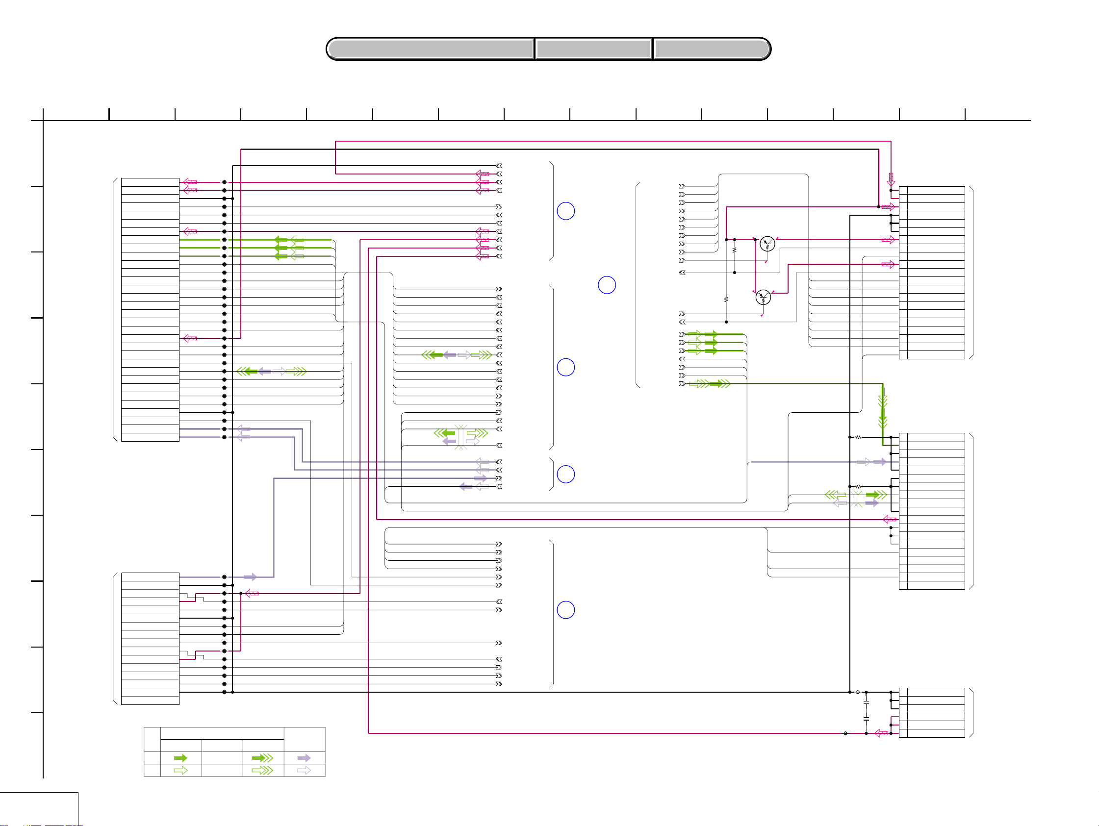
DSC-T1
For Schematic Diagram
• Refer to page 4-47 for printed wiring board.
1
25 15
SY-95 BOARD(8/8)
CONNECTOR(CN,FP BLOCK)
A
XX MARK:NO MOUNT
NO MARK:REC/PB MODE
PANEL_13.5V
PANEL_2.8V
REG_GND
BL_LEV
B
C
THROUGH THE
FP-691 FLEXIBLE
()
(PAGE 4-32)
D
E
TO
MS-148 BOARD
BL_THH
LED_K
LED_A
PANEL_B
PANEL_G
PANEL_R
XRST_SYS
SYS_SI
XPANEL_TG_CS
XSYS_SCK
SYS_SO
BL_MODE
PANEL_V
HD0
XACCESS_LED
D_2.8V
MS_PWR_ON
MSCLK
MS_IN
MS_DIO
MSDS
MSD3
MSD2
MSB1
MS_REG_GND
MODE_DIAL
SP+
SP-
F
G
MIC_IN
REG_GND
XPOWER_LED_ON
EVER_3.0V
TO
H
CONTROL SWITCH BLOCK
(PW-125)
CN001
THROUGH THE
FP-693 FLEXIBLE
()
(PAGE 4-13
of LEVEL2)
I
XPOWER_ON
REG_GND
XAE_LOCK_ON
XHTR_SW
XRESET_SW
XCHARGE/XSTRB_LED
EVER_3.0V
KEY_AD0
KEY_AD1
KEY_AD2
REG_GND
NC
SIGNAL PATH
J
16
CHROMA SIGNALY/CHROMAY
REC
PB
CL901
CL902
CL903
CL904
CL905
CL906
CL907
CL908
CL909
CL910
CL911
CL912
CL913
CL914
CL915
CL916
CL917
CL918
CL919
CL920
CL921
CL922
CL923
CL924
CL928
CL927
CL926
CL925
CL929
CL931
CL934
CL935
CL961
CL962
CL957
CL955
CL960
CL956
CL954
CL952
CL951
CL968
CL969
CL953
CL949
CL950
CL970
VIDEO SIGNAL
XPANEL_TG_CS
XACCESS_LED
MS_PWR_ON
AUDIO
PANEL_B
PANEL_G
PANEL_R
XRST_SYS
SYS_SI
XSYS_SCK
SYS_SO
BL_MODE
PANEL_V
HD0
MC_MSCLK
MC_MSDI0
MC_MSDS
MC_MSD3
MC_MSD2
MC_MSB1
XAE_LOCK_ON
XSHTR_ON
4-2. SCHEMATIC DIAGRAMS
4-2. SCHEMATIC DIAGRAMS
SYS_SI
XPANEL_TG_CS
XSYS_SCK
SYS_SO
BL_MODE
XACCESS_LED
MS_PWR_ON
MC_MSCLK
MC_MSDIO
MC_MSD1
MC_MSD2
MC_MSD3
MC_MSBS
XSHTR_ON
XAE_LOCK_ON
LENS_TEMP
XCAM_DR_PS
USBPHY_D-
USBPHY_D+
AU_OUT
USB_JACK_IN
XMULTI_JACK_IN
BATT/XEXT
AV_JACK_IN
810 137
REG_GND
M_5V
PANEL_13.5V
D_2.8V
BL_LEV
BL_THH
LED_K
LED_A
EVER_3.0V
ACV_UNREG
VL_3V
SYS_SI
XPANEL_TG_CS
XSYS_SCK
SYS_SO
BL_MODE
XACCESS_LED
MS_PWR_ON
MC_MSCLK
MC_MSDIO
MC_MSD1
MC_MSD2
MC_MSD3
MC_MSBS
XSHTR_ON
XAE_LOCK_ON
LENS_TEMP
XCAM_DR_PS
USBPHY_D-
USBPHY_D+
SP+
SP-
MIC_IN
AU_OUT
USB_JACK_IN
XMULTI_JACK_IN
BATT/XEXT
AV_JACK_IN
XMS_IN
MODE_DIAL0
XPOWER_LED_ON
XPWR_ON
XRESET_SW
XCHARGE/XSTRB_LED
KEY_AD0
KEY_AD1
KEY_AD2
SY-95 BOARD SIDE A SY-95 BOARD SIDE B
SY-95 BOARD SIDE A SY-95 BOARD SIDE B
11
HR_EN0
HR_DIR0B
HR_DIR0A
HR_EN2
HR_DIR2B
HR_DIR2A
HR_EN3
HR_DIR3B
HR_DIR3A
PANEL_B
PANEL_G
PANEL_R
XRST_SYS
PANEL_V
HD0
2.8 0
R706
68k
R707
68k
HD0
DTA143TMT2L
2.9
AU_OUT
20
13
17
16
(7/8)
(3/8)
(5/8)
(4/8)
HR_EN0
HR_DIR0B
HR_DIR0A
HR_EN2
HR_DIR2B
HR_DIR2A
HR_EN3
HR_DIR3B
HR_DIR3A
XFC_RST_LED
XFC_RST_SENS
(2/8)
4
XZM_RST_LED
XZM_RST_SENS1
PANEL_B
PANEL_G
PANEL_R
XRST_SYS
PANEL_V
V_OUT
Q702
SWITCH
2.9
Q703
DTA143TMT2L
SWITCH
USB_JACK_IN
XMULTI_JACK_IN
BATT/XEXT
AV_JACK_IN
129
LENS_TEMP
HR_EN0
USBPHY_D-
USBPHY_D+
HR_DIR0B
HR_DIR0A
HR_EN2
HR_DIR2B
HR_DIR2A
HR_EN3
HR_DIR3B
HR_DIR3A
XCAM_DR_PS
FB704
0
Note
FB703
0
Note
Note:Resestor is mounted to the location
FB703 and FB704 are printed.
FB702
0uH
C702
0.1u
C701
FB701
0uH
0.1u
02.8
14463
21PCN701
1 M_5V
2 M_5V
3 D_2.8V
4 REG_GND
5 REG_GND
6 REG_GND
7 F_RST_VCC
8 XFC_RST_SENS
9 LENS_TEMP
10 Z_RST_VCC
11 XZM_RST_SENS
12 HR_EN0
13 HR_DIR0B
14 HR_DIR0A
15 HR_EN2
16 HR_DIR2B
17 HR_DIR2A
18 HR_EN3
19 HR_DIR3B
20 HI_DIR3A
21 XCAM_DR_PS
19PCN704
1 REG_GND(AU)
2 V_OUT
3 REG_GND(AU)
4 AU_OUT
5 REG_GND(AU)
6 REG_GND(USB)
7 REG_GND(USB)
8 USBPHY_D-
9 USBPHY_D+
10 REG_GND(USB)
11 VL_3V
12 VBUS
13 VBUS
14 VBUS
15 XMULTI_IN
16 NC
17 BATT/XEXT
18 XAV_JACK_IN
19 NC
6P
CN705
1 ACV_GND
2 ACV_GND
3 ACV_GND
ACV_UNREG0
4
ACV_UNREG0
5
ACV_UNREG0
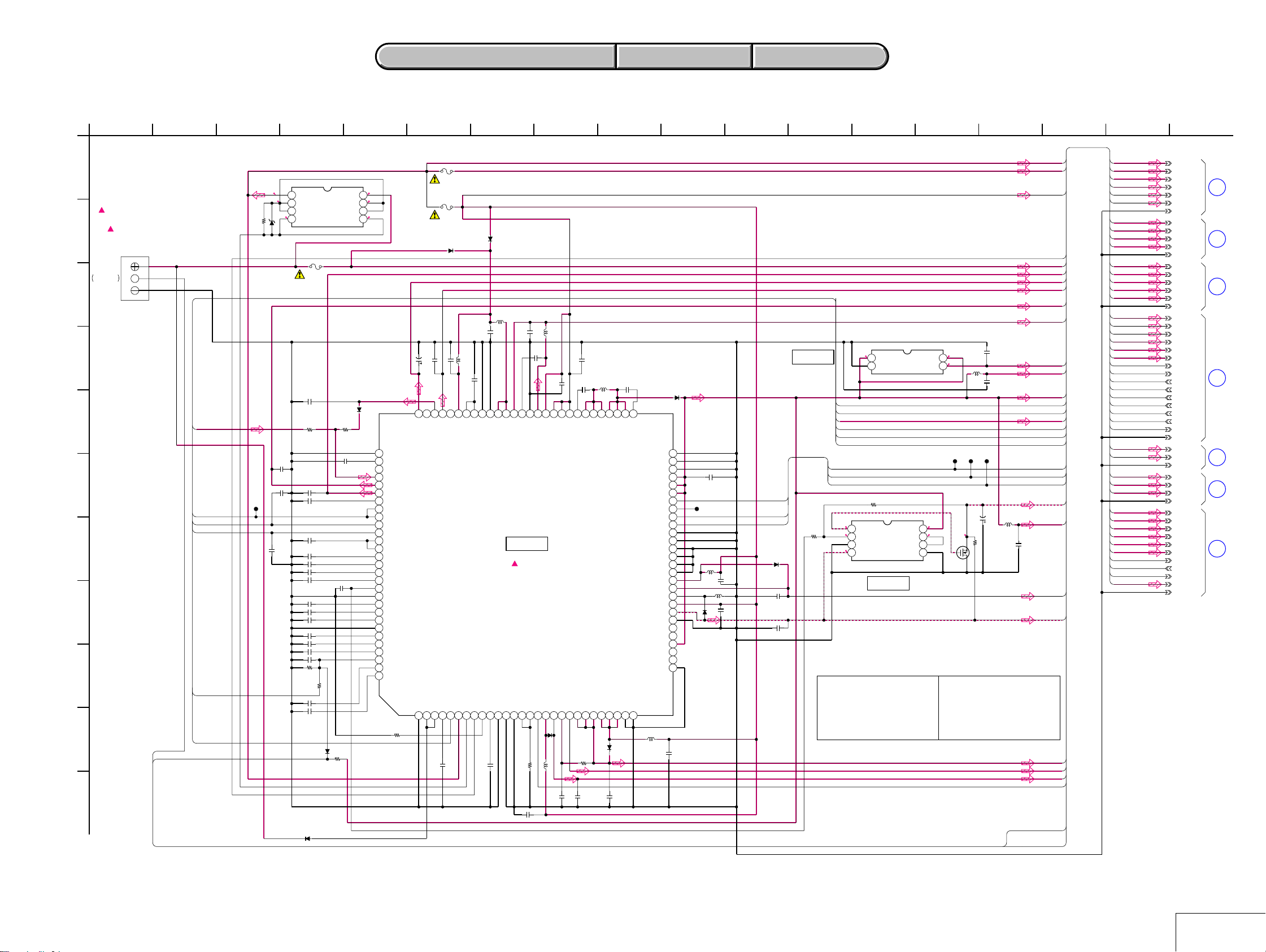
6
TO
LD-140 BOARD
THROUGH THE
FP-695 FLEXIBLE
(PAGE 4-36)
TO
CN-198 BOARD
(PAGE 4-9
of LEVEL2)
TO
CN-198 BOARD
(PAGE 4-9
of LEVEL2)
)(
SY-95 (8/8)
4-29 4-30
Page 13
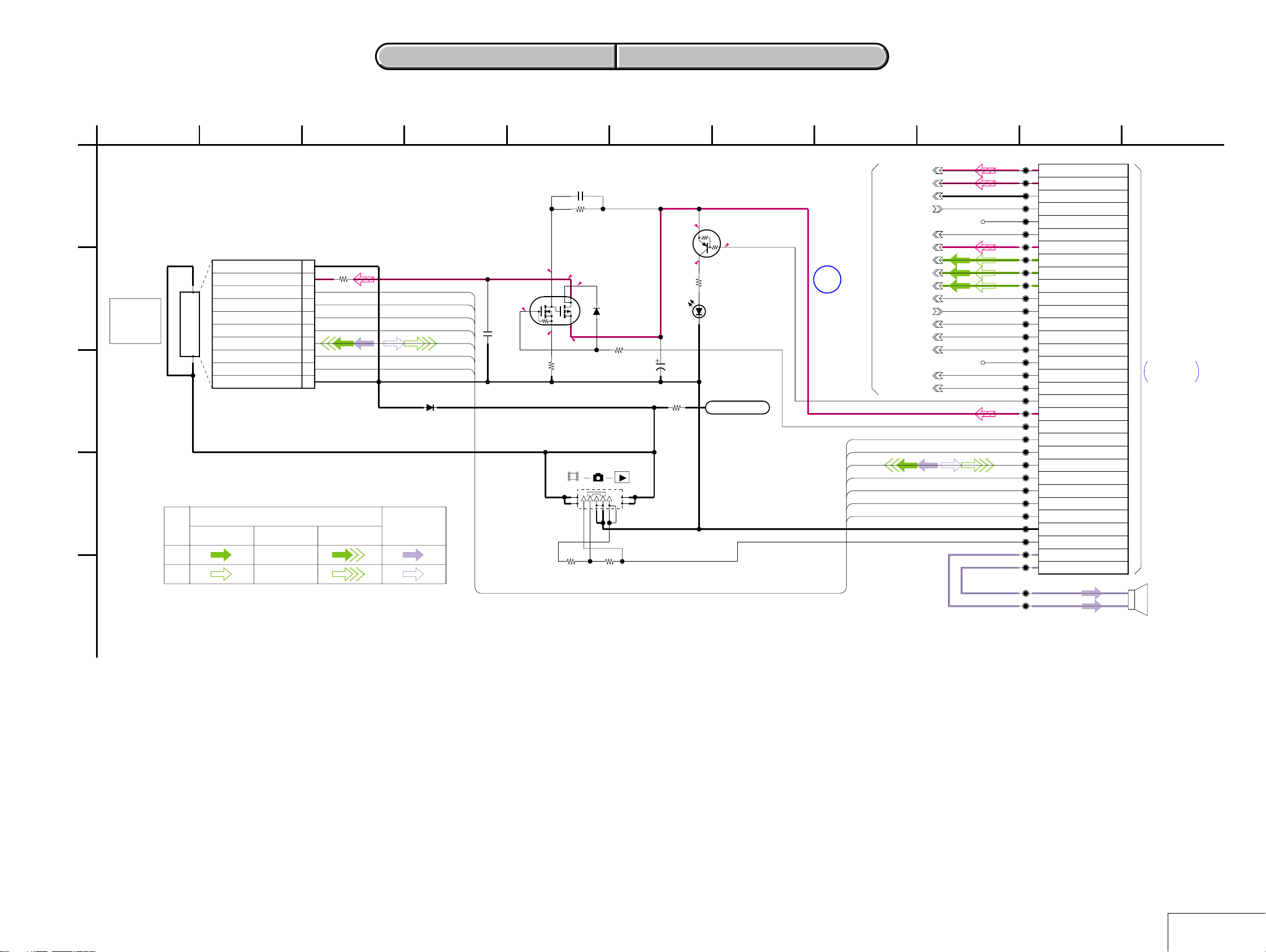
For Schematic Diagram
• Refer to page 4-51 for printed wiring board.
4-2. SCHEMATIC DIAGRAMS MS-148 PRINTED WIRING BOARD
4-2. SCHEMATIC DIAGRAMS MS-148 PRINTED WIRING BOARD
DSC-T1
1
MS-148 BOARD(1/2)
MS I/O(CN BLOCK)
A
XX MARK:NO MOUNT
NO MARK:REC/PB MODE
B
MEMORY
STICK
DUO
CONNECTOR
C
D
REC
E
SDIO/DATA0
SIGNAL PATH
VIDEO SIGNAL
CHROMA
PB
CN101
SCLK
DATA3
DATA2
DATA1
GND
VCC
GND
Y
(2/2)
MSCLK
MS_IN
MS_DIO
MSBS
MSD3
MSD2
MSD1
8107
PANEL_13.5V
PANEL_2.8V
REG_GND
BL_LEV
LED_K
LED_A
PANEL_B
PANEL_G
PANEL_R
XRST_SYS
SYS_SI
XPANEL_TG_CS
XSYS_SCK
SYS_SO
PANEL_V
HDO
925
CL101
CL102
CL103
CL104
CL105
CL106
CL107
CL108
CL109
CL110
CL111
CL112
CL113
CL114
CL115
CL116
CL117
CL118
CL119
CL120
CL121
CL122
CL123
CL124
CL125
CL143
CL144
CL145
CL126
CL128
CL131
CL132
CL158
CL157
PANES_13.5V
PANEL_2.8V
REG_GND
BL_LEV
BL_THH
LED_K
LED_A
PANEL_B
PANEL_G
PANEL_R
XRST_SYS
SYS_SI
XPANEL_TG_CS
XSYS_SCK
SYS_S0
BL_MODE
PANEL_V
HD0
XACCESS_LED
D_2.8V
MS_PWR_ON
MSCLK
MS_IN
MS_DI0
MSBS
MSD3
MSD2
MSD1
MS_REG_GND
MODE_DIAL
SP+
SP-
11
TO
SY-95 BOARD
(8/8)
THROUGH
THE FP-691
FLEXIBLE
(PAGE 4-29)
SP901
(SPEAKER)
463
C103
0.1u
B
R104
220k
10P
10
R107
9
8
7
INT
6
5
4
3
2
BS
1
0
D101
XX
MSCLK
MSD3
MS_IN
MSD2
MS_DIO
MSD1
MSBS
SSM6E01TU
SWITCH
C101
XX
B
Q101
2.9
2.9
2
2.9
2.9
1
4
5
D102
MA2SD32008S0
3
6
0
R101
3300
2.9
S101
(MODE SW)
R106
2200
C102
22u
6.3V
R108
2.9
0
R105
820
SML-310LTT86
A
LND101
XX
AUDIO
Y/CHROMA SIGNAL
R102
1500
R103
1200
DTA144EMT2L
LED DRIVE
2.9
D103
(ACCESS)
STATIC_GND
Q102
1
16
4-31 4-32
MS-148 (1/2)
Page 14
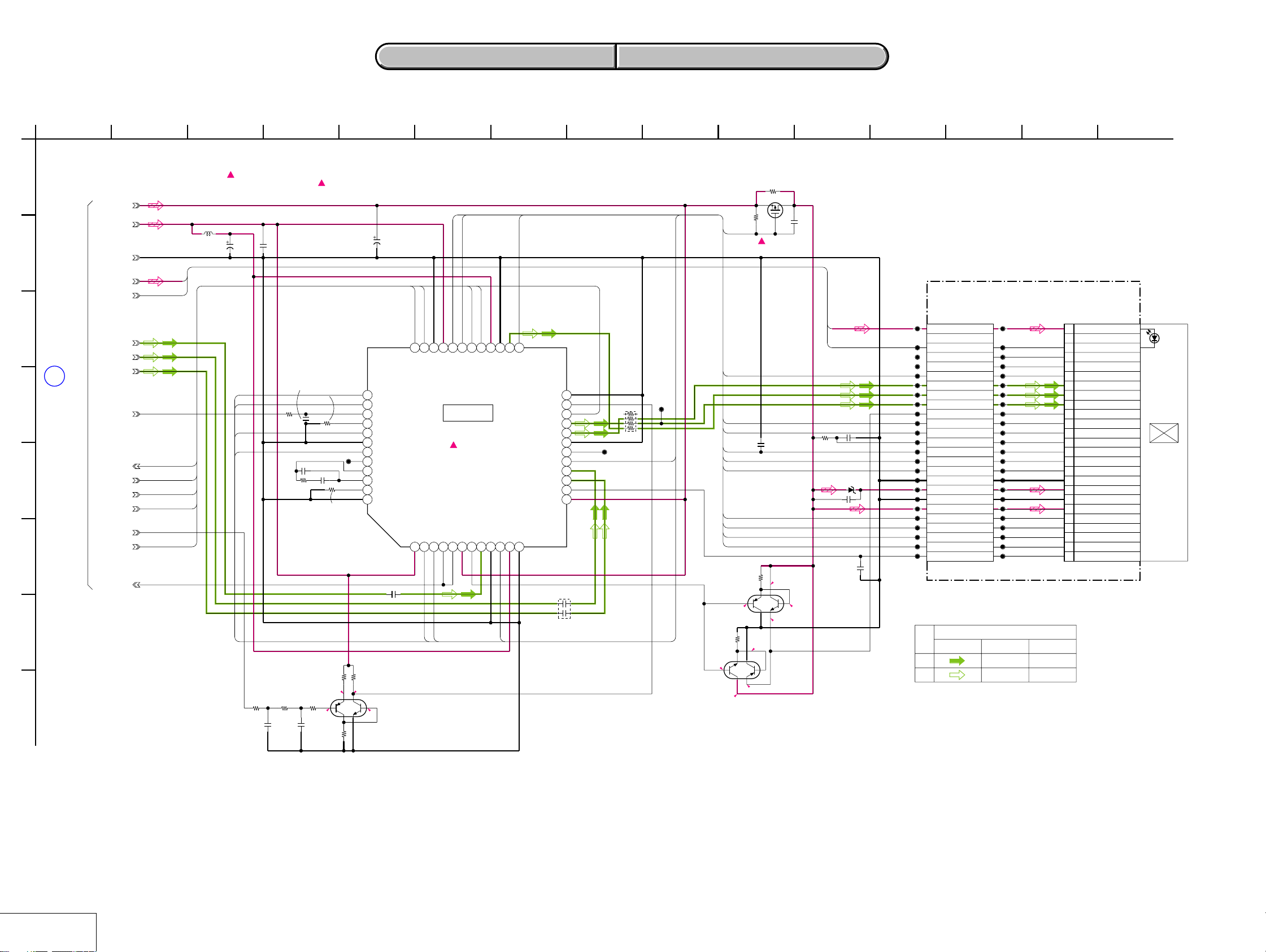
DSC-T1
For Schematic Diagram
• Refer to page 4-51 for printed wiring board.
4-2. SCHEMATIC DIAGRAMS MS-148 PRINTED WIRING BOARD
4-2. SCHEMATIC DIAGRAMS MS-148 PRINTED WIRING BOARD
1
MS-148 BOARD(2/2)
LCD PANEL DRIVE(PD BLOCK)
A
XX MARK:NO MOUNT
PANEL_13.5V
PANEL_2.8V
B
C
(1/2)
1
D
E
XPANEL_TG_CS
F
G
H
16
REG_GND
LED_A
LED_K
PANEL_B
PANEL_G
PANEL_R
XRST_SYS
SYS_SI
XSYS_SCK
SYS_SO
PANEL_V
BL_LEV
810 137
11
12925 15
14463
NO MARK:REC/PB MODE
:Voltage measurement of the CSP IC
and the Transistors with mark,is
not possible.
Q801
BUFFER
XPOFF
RGT
HCK1
HCK2
REF
HST
WIDE
DWN
EN
VCK
VST
Q802
UP04601008S0
BUFFER
R815
10k
7.0
2
13.5
6
WIDE
HCK2
SYS_SO
E3SIE4
E5
E6
E7
SCK
VDD
WIDE
HCK2
GND1
IC803
RGB DRIVE,
TIMING GENERATOR
IC803
CXA3622GG
CSP(CHIP SIZE PACKAGE)IC
DWN
XPANEL_TG_CS
E1
E2
XCS
VCC1
XPOFF
D6VRD7
D5
GND2
XPOFF
TEST
D3
XVD
D2
HDO
HD
D1
VG
C7
VB
C6
N.C
C5
PWM
VCK
Gin
Rin
COM
VCC2
C819
EN
0.01u
CL801
C4
C3
C2
C1
B7
B6
RB801
10X4
CL802
VCK
UP04601008S0
R831
22k
2.8
1
C810
2.2u
25V
HCK1
F3
REF
F4
XCLR
F5
Filter1
F6
HST
F7
CLK/XWRT
G1
RGT
G2
HDO
G3
OP_OUT
G4
OP_IN
G5
Filter2
G6
VSS
G7
C805
2
02.8
Q805
UP04601008S0
LPF
TA
A
SYS_SI
XSYS_SCK
F1
F2
SO
VDDA2VSTA3DWNA4F_BACKA5EXTDAA6VCC3A7VPB1BinB2VSSB3ENB4BLDETB5XLED
A1
B
0.01u
VST
C820
C808
0.1u
B
47u
6.3V
R809
10k
C822
HCK1
REF
HST
RGT
R826
82k
±0.5%
C823
150p
CH
C812
R827
82k
±0.5%
560p
R821
C824
220p
CH
CH
±0.5%
XX
1/16W
0
CL803
0.1u
C811
R808
68k
R810
100k
±0.5%
1/16W
R830
10k
2.8
R828
46
4700
±0.5%
5
3
R829
10k
L802
47uH
LED_A
LED_K
SYS_SI
XPANEL_TG_CS
XSYS_SCK
SYS_SO
HDO
HDO
R820
100k
5
7.0
1
R832
SSM3J09FU(TE85L)
C814
0.1u
R818
10k
4
3
6.4
3
5
4
7.0
XX
C821
0.01u
Q803
REG,
LED_A
LED_K
BL_THH
BL_THL
CREXT
REG_GND
VDDG
REG_GND
N.C.
RGT
PSIG
HCK1
HCK2
REF
HST
WIDE
VDD
DWN
VCK
VST
COM
VB
VR
VG
EN
FLEXIBLE
CL401
CL402
CL403
CL404
CL405
CL406
CL407
CL408
CL409
CL410
CL411
CL412
CL413
CL414
CL415
CL416
CL417
CL418
CL419
CL420
CL421
CL422
CL423
CL424
CN402
25P
LED_A1
N.C.2
LED_K3
BL_THH4
BL_THL5
RGT6
VB7
VR8
VG9
PSIG10
HCK111
HCK212
CREXT13
REF14
HST15
WIDE16
REG_GND17
VDDG18
VSS19
VDD20
DWN21
EN22
VCK23
VST24
COM25
ND901
BACK
LIGHT
LCD901
2.5INCH
COLOR LCD
UNIT
(ACX500EN-J)
FP-694
LED_A
LED_K
R819
B
13.5
6
2
1
7.0
150k
7.6
C817
MA8036-TX
C816
C813
4.7u
D801
B
0.1u
1u B
B
CL804
CL805
CL806
CL807
CL808
CL809
CL810
CL811
CL812
CL813
CL814
CL815
CL816
CL817
CL818
CL819
CL820
CL821
CL822
CL823
CL824
CL825
CL826
CL827
SIGNAL PATH
VIDEO SIGNAL
CHROMA Y/CHROMAY
REC
PB
MS-148 (2/2)
4-33 4-34
Page 15
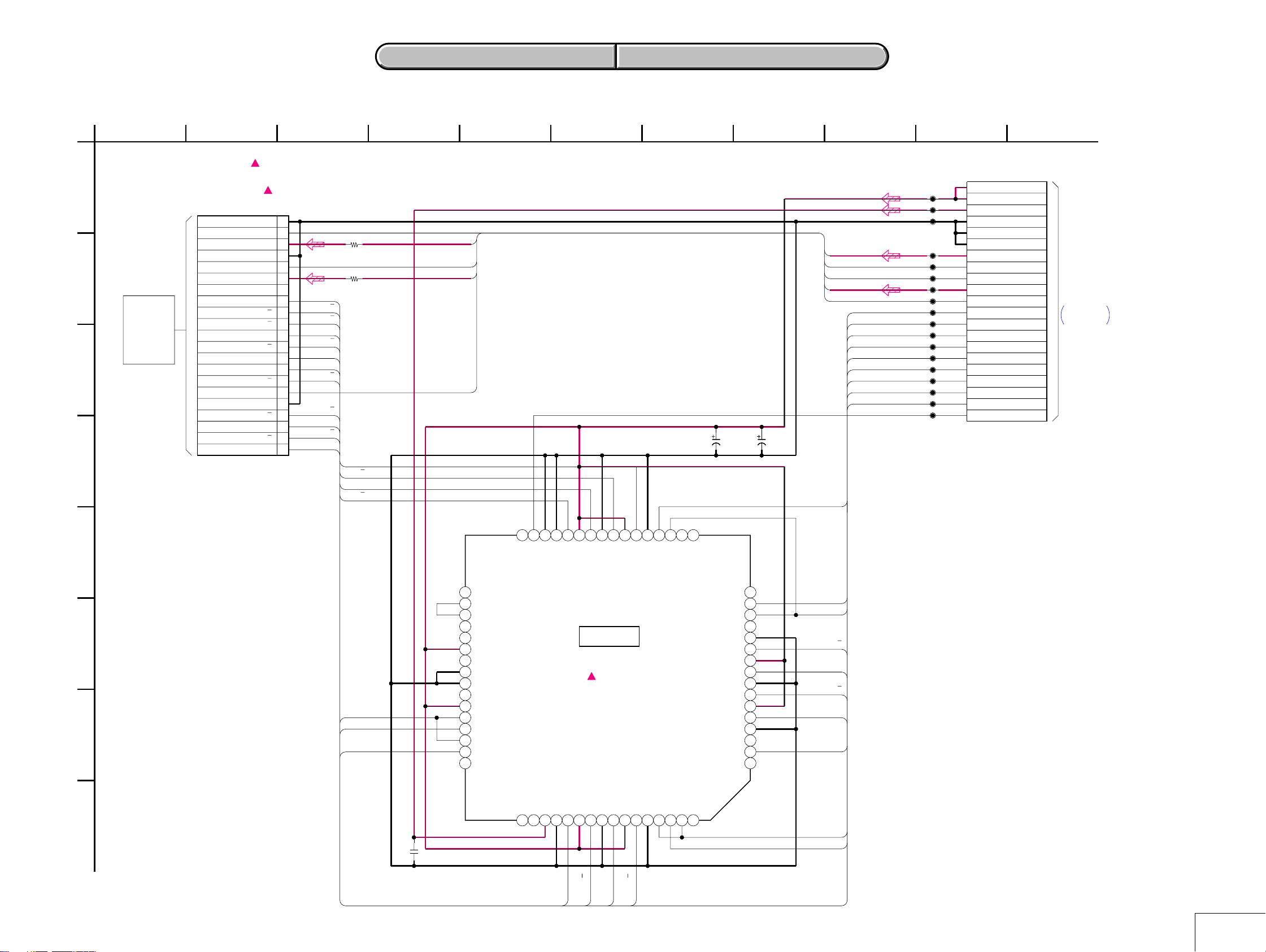
For Schematic Diagram
• Refer to page 4-45 for printed wiring board.
4-2. SCHEMATIC DIAGRAMS LD-140 PRINTED WIRING BOARD
4-2. SCHEMATIC DIAGRAMS LD-140 PRINTED WIRING BOARD
DSC-T1
1
LD-140 BOARD
A
LENS DRIVE
XX MARK:NO MOUNT
B
LENS
UNIT
(LSV-850A)
C
D
LENS UNIT is replaced as a block.
So that there PRINTED WIRING BOARD and
SCHEMATIC DIAGRAM are omitted.
:Voltage measurement of
the CSP IC and
the Transistors with
mark,is not possible.
CN002
21P
1Z_RST_GND
2Z_RST_SENS
3Z_RST_VCC
4F_RST_GND
5F_RST_SENS
6F_RST_VCC
7N.C
FOCUS_A
8FOCUS_A
FOCUS_B
9FOCUS_B
FOCUS_A
10FOCUS_A
FOCUS_B
11FOCUS_B
ZOOM_A
12ZOOM_A
ZOOM_A
13ZOOM_A
ZOOM_B
14ZOOM_B
ZOOM_B
15ZOOM_B
16TEMP_OUT
17TEMP_GND
18IRIS_A
19IRIS_A
20IRIS_B
21IRIS_B
IRIS_A
IRIS_A
IRIS_B
IRIS_B
R002
IRIS_A
IRIS_A
IRIS_B
IRIS_B
8107463 11925
CL001
CL002
XZM_RST_SENS
220
220R001
Z_RST_VCC
XFC_RST_SENS
F_RST_VCC
LENS_TEMP
C009
F_RST_VCC
XFC_RST_SENS
LENS_TEMP
Z_RST_VCC
XZM_RST_SENS
HR_EN0
HR_DIR0B
HR_DIR0A
HR_EN2
HR_DIR2B
HR_DIR2A
HR_EN3
HR_DIR3B
HR_DIR3A
C008
XX
22u
10V
HR_DIR3B
CL003
CL004
CL005
CL006
CL007
CL008
CL009
CL010
CL011
CL012
CL013
CL014
CL015
CL016
CL017
CL018
M_5V
M_5V
D_2.8V
REG_GND
REG_GND
REG_GND
F_RST_VCC
XFC_RST_SENS
LENS_TEMP
Z_RST_VCC
XZM_RST_SENS
HR_EN0
HR_DIROB
HR_DIR0A
HR_EN2
HR_DIR2B
HR_DIR2A
HR_EN3
HR_DIR3B
HR_DIR3A
XCAM_DR_PS
TO
SY-95 BOARD
(8/8)
CN701
THROUGH
THE FP-695
FLEXIBLE
(PAGE 4-30)
E4H1H2G3H3G4F4H4H5G5F5H6G6H7G7F6
PS
E
NC
E5H8G8F7F8E6E7E8D8D7D6C8C7B8B7C6
VLIM
VREF
EN7
F
HR_EN2HR_EN2
HR_DIR2A
G
HR_DIR2B
IN7
VM4
OUT7A
RNFS
RNF
OUT7B
VM4
EN3
IN3
EN4
IN4
NC
NC
NC
NC
D5 A8 A7 B6 A6 C5 B5 A5 A4 C4 B4 A3 B3 A2 B2 C3
VM1
DGND
OUT2B
OUT2A
PGND1
IC001
FOCUS/ZOOM MOTOR DRIVE,
IRIS DRIVE
M50237WG-DF0T
CSP(CHIP SIZE PACKAGE)IC
VM2
OUT3A
VCC
PGND2
OUT3B
IC001
PGND2
PGND1
OUT1B
OUT4A
VM2
VM1
OUT1A
OUT4B
PGND1
PGND2
IN2
EN5
H
C001
16
0.1u
EN2
IN5
NC
EN6
NC
NC
IN1
EN1
BR6
PGND3
OUT6B
VM3
OUT6A
PGND3
OUT5B
VM3
OUT5A
PGND3
BR5
IN6
NC
D4 A1 B1 C2 C1 D3 D2 D1 E1 E3 E2 F1 F2 G1 G2 F3
NC
HR_DIR3A
HR_EN3
ZOOM_B
ZOOM_B
ZOOM_A
ZOOM_A
HR_DIR0B
HR_EN0
HR_DIR0A
FOCUS_A
FOCUS_A
FOCUS_B
FOCUS_B
4-35 4-36
LD-140
Page 16

1. Before starting adjustment
EVR Data Re-writing Procedure When Replacing Board
The data that is stored in the repair board, is not necessarily correct.
Perform either procedure 1 or procedure 2 or procedure 3 when replacing board.
Procedure 1
Save the EVR data of the machine in which a board is going to be replaced. Do wnload the saved data after a board
is replaced.
(Machine before starting repair)
SECTION 6
ADJUSTMENTS
PC PC
DSC-T1
(Machine after a board is replaced)
Save the EVR data
to a personal computer.
Download the saved
data to a machine.
Procedure 2
Remove the EEPR OM from the board of the machine that is going to be repaired. Install the removed EEPR OM
to the replaced board.
Remove the EEPROM and install it.
(Former board)
(New board)
Procedure 3
When the data cannot be saved due to defective EEPROM, or when the EEPROM cannot be removed or
installed, save the data from the same model of the same destination, and do wnload it.
(Machine to be repaired) (Machine to be repaired)
PC
Save the data.
(The same model of the same destination)
After the EVR data is saved and downloaded, check the
respective items of the EVR data.
(Refer to page 6-2 for the items to be checked.)
Download the data.
6-1
Page 17
DSC-T1
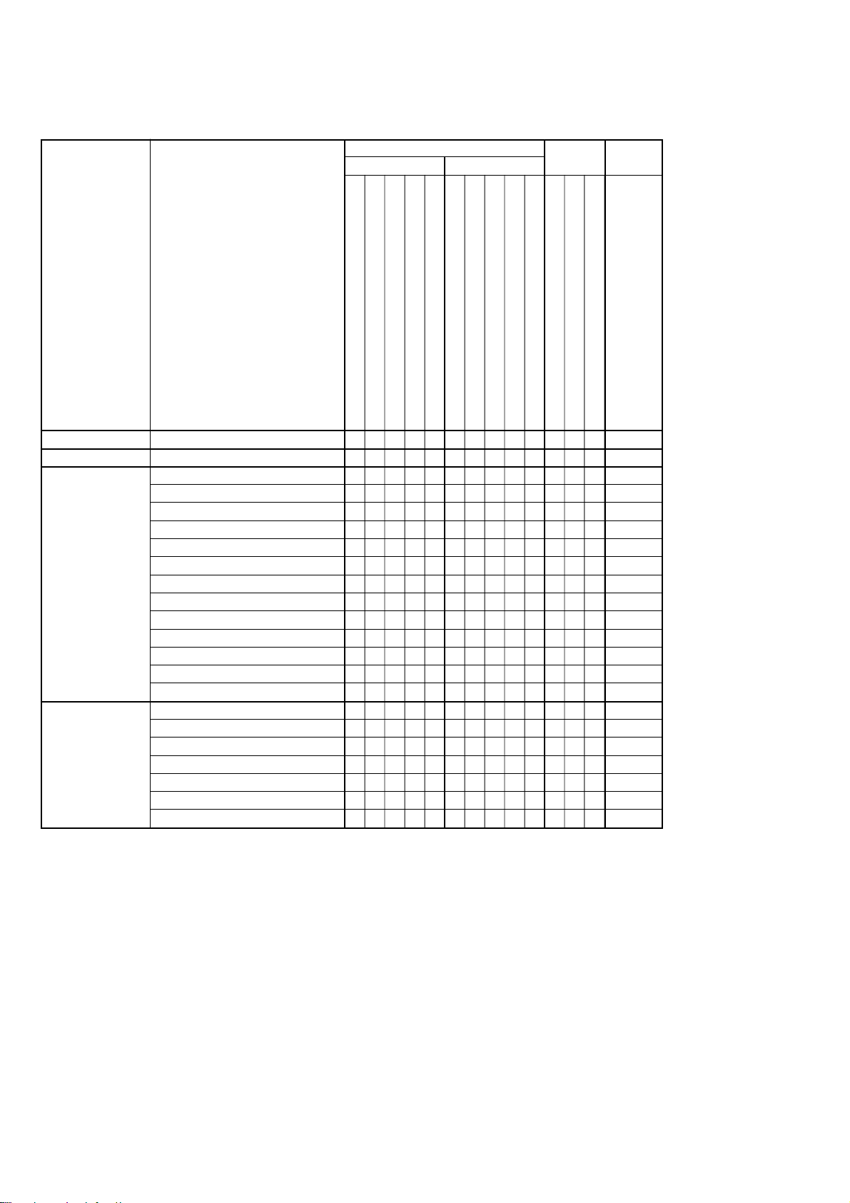
1-1. Adjusting items when replacing main parts and boards.
When replacing main parts and boards, adjust the items indicated by z in the following table.
Replaced parts Board
Block replacement
Parts replacement
replacement
EEPROM
replacement
Adjustment
Section
Initialization of data
Video
Camera
LCD
Adjustment
Initialization of data
Video output level adj.
Wide limit Adj.
Flange back adj.
F No. compensation
Mechanical shutter adj.
Light value adj.
AWB 3200K standard data input
AWB 5800K standard data input
CCD linearity check
Color reproduction adj.
CCD white defect compensation check
CCD black defect compensation check
Strobe adj.
Auto focus illumination check
LCD initial data input
VCO adj.
Bright adj.
Contrast adj.
V COM adj.
White balance adj. (1)
White balance adj. (2)
Table. 6-1-1.
IC803 (RGB drive, Timing.gen.) (LCD)
IC151 (Timing gen. S/H, AGC A/D con v.)
CCD block
Lens device
Xenon tube
LCD block LCD unit (LCD901)
LCD block Back light unit
MS-148 board
ST-86 board D003 (AF Illumination LED)
SY-95 board
SY-95 board IC301 (Camera DSP)
SY-95 board IC302 (Video amp.)
MS-148 board (COMPLETE)
ST-86 board (COMPLETE)
SY-95 board (COMPLETE)
SY-95 board IC501 (Camera system control)
(With built-in flash memory)
zz
zz z z
zzz
zz z z
zz z z z
zz z z z
zz z z z
zz z z z
zz z z z
zz z z z
zz z z z
zz z z z
zz z z z
zzz z z z
zzzzzz
zz
zzzz
zzzz
zzzzz
zz zzz
zzz z z z
zzz z z z
6-2
Page 18
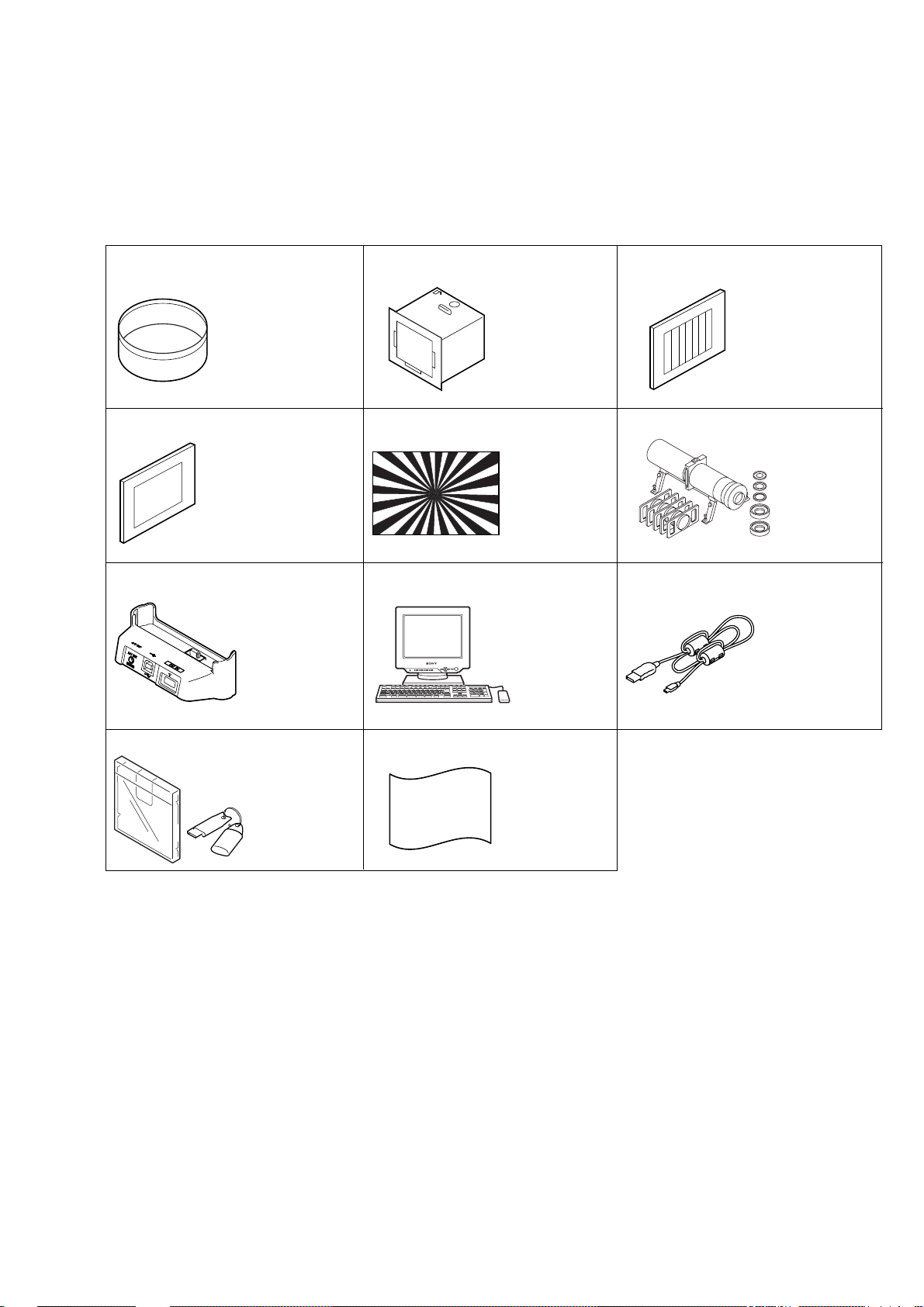
6-1. ADJUSTMENT
1-1. PREPARATIONS BEFORE ADJUSTMENT
1-1-1. List of Service Tools
• Oscilloscope • Color monitor • Vectorscope • AC power adapter
• Calculator which can hexadecimal calculation.
DSC-T1
J-1 J-2 J-3
Filter for color
temperature correction
(C14)
J-6080-058-A
J-4
J-7 J-8
Clear chart for
pattern box
For PTB-450:
J-6080-621-A
For PTB-1450:
J-6020-560-A
Cradle
1-817-742-11
J-5
Pattern box PTB-450
J-6082-200-A
or
Pattern box PTB-1450
J-6082-557-A
J-6
Siemens star chart
J-6080-875-A
J-9
Personal computer
with Windows98/
98SE/ME/2000/XP
installed and with
two USB ports
Clear chart for
pattern box
For PTB-450:
J-6020-250-A
For PTB-1450:
J-6020-559-A
Mini pattern box
J-6082-353-B
USB cable
1-823-073-11
J-10
Application for
adjustment (SEUS)
and HASP key
(Note)
Note : Contact our service headquarter of each area how to get the application for adjustment (SEUS) and HASP key.
J-11
Backgorund
paper
J-2501-130-A
Fig. 6-1-1.
6-3
Page 19
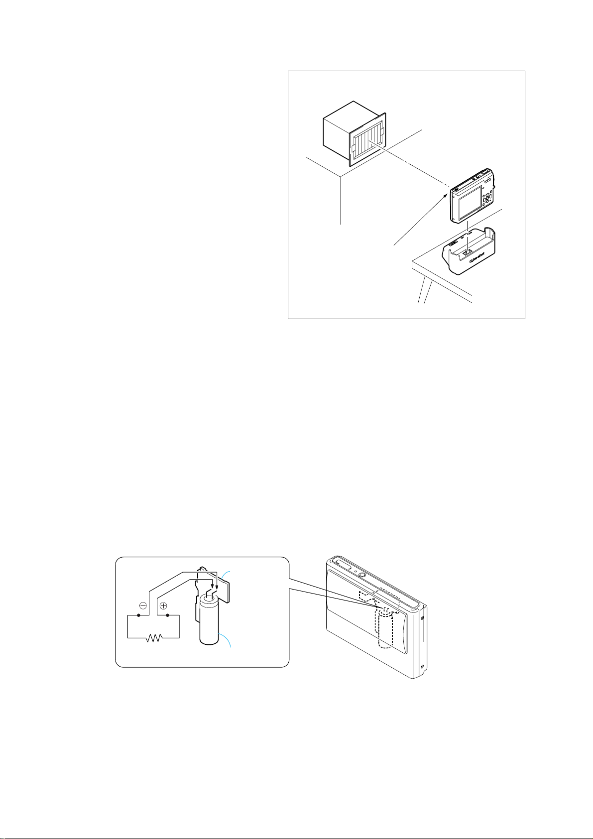
DSC-T1
1-1-2. Preparations
1) Connect the equipment for adjustments according to Fig. 6-1-4.
2) Start up the application for adjustment (SEUS).
Note1: Setting the “Forced Power ON Mode (Forced STILL Mode)”
1) Select page: 00, address: 01, and set data: 01.
2) Select page: 2F, address: 23, and write data: 01.
3) Save the data.
4) Wait for 3 sec.
The above procedure will enable the power (STILL mode) to
be turned on with POWER switch (Control switch block)
disconnected. After completing adjustments, be sure to exit the
“Forced Power ON Mode”.
Note2: Setting the “Forced Power ON Mode (Forced PLAY Mode)”
1) Select page: 00, address: 01, and set data: 01.
2) Select page: 2F, address: 23, and write data: 02.
3) Save the data.
4) Wait for 3 sec.
The above procedure will enable the power (PALY mode) to be
turned on with POWER switch (Control switch block)
disconnected. After completing adjustments, be sure to exit the
“Forced Power ON Mode”.
Note3: Exiting the “Forced Power ON Mode”
1) Select page: 00, address: 01, and set data: 01.
2) Select page: 2F, address: 23, and write data: 80.
3) Save the data.
4) Wait for 3 sec.
5) Select page: 00, address: 01, and set data: 00.
1-1-3. Discharging of the flashlight power supply
The capacitor which is used as power supply of flashlight is charged
with 200V to 300V voltage. When disassembling the unit, dischar ge
this voltage in order to protect service engineers from electric shock.
Pattern box
About 12cm (PTB-1450)
About 30cm (PTB-450)
Front of the lens
Fig. 6-1-2.
Discharge procedure
1. Remove the power supply (AC power adaptor or battery).
2. Fabricate the discharging jig as sho wn in Fig. 6-1-3 locall y by
yourself. Connect the discharging jig to the positive (+) and
negative (-) terminal of the flash v oltage charge capacitor . Allo w
ten seconds to discharge the voltage.
ST-86 BOARD
Shorting jig
(1kΩ / 1w)
Capacitor
Fig. 6-1-3.
6-4
Page 20
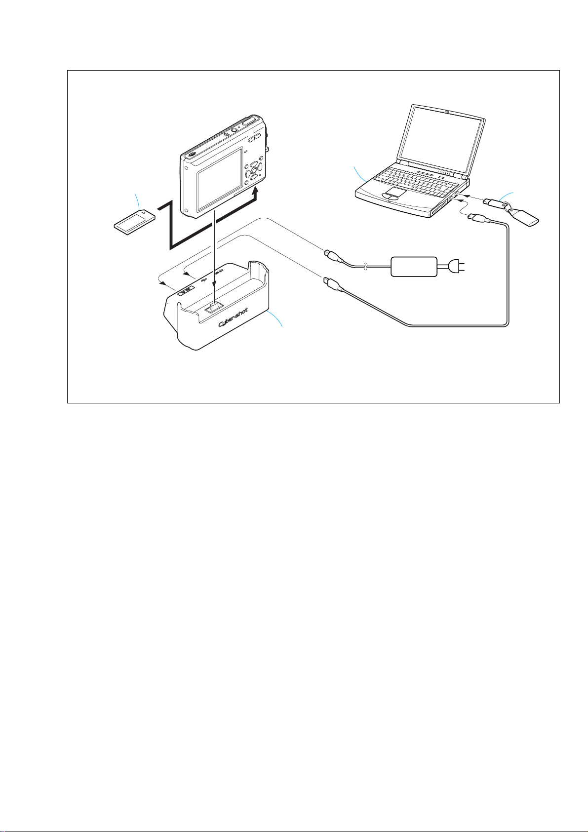
Memory stick DUO
Cradle
Personal computer
(with two USB ports)
AC IN
DC IN
USB
USB1
USB2
HASP key
AC power
adaptor
[CONNECTION OF EQUIPMENT]
DSC-T1
Note: When performing “Flange Back Adjustment”, connect the cables after
disassembling the cradle. Unless the cradle is disassembled, the USB
cable and the power cable will interfere with the flange back adjustment
jig or mini pattern box, and thus the subject cannot be set correctly.
Fig. 6-1-4
6-5
Page 21
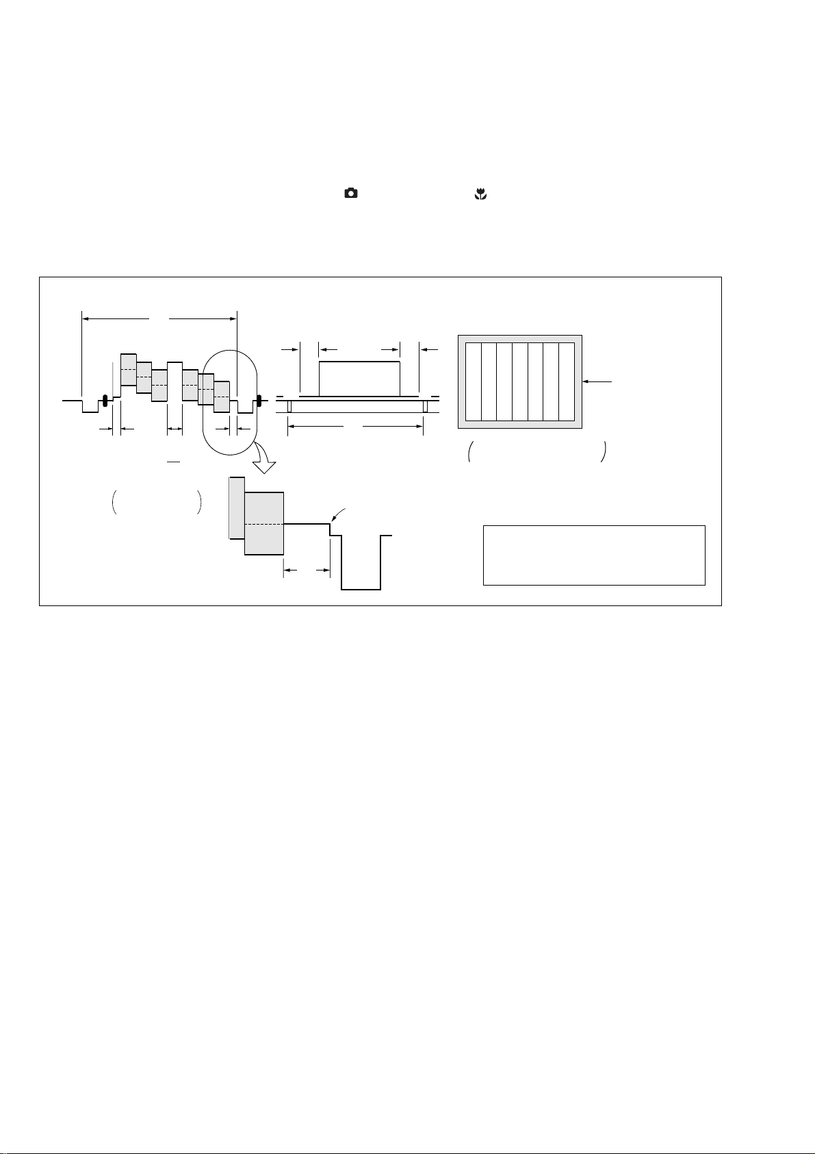
DSC-T1
e
1-1-4. Precaution
1. Setting the Switch
Unless otherwise specified, set the switches as follows and perform
adjustments.
Switch settings
1. Mode switch....................................................... STILL (
2. Lens cover...................................................................... Open
3. ZOOM.................................................................... WIDE end
2. Order of Adjustments
Basically carry out adjustments in the order given.
Color bar chart (Standard picture frame)
H
)
3. MACRO (
) .................................................................. ON
4. SCENE (Menu)............................................................... Auto
5. VIDEO OUT (SET UP of Menu) .................................NTSC
Yellow
Cyan
Green
AAB
B
A=
2
Fig. a
Video terminal
output waveform
White
Magenta
Red
Blue
CD
Enlargement
A
3. Subjects
1) Color bar chart (Standard picture frame)
When performing adjustments using the color bar chart, adjust
the picture frame as shown in Fig. 6-1-5. (Standard picture
frame)
2) Clear chart (Color reproduction adjustment frame)
Remove the color bar chart from the pattern box and insert a
clear chart in its place. (Do not perform zoom operations during
this time.)
C=D
V
Difference in level
Fig.6-1-5.
Cyan
White
Green
Yellow
LCD screen or under scan
Fig. b
monitor TV picture
Adjust the camera position and direction to
obtain the output wavef orm shown in Fig. a
and the LCD screen or the monitor TV
display shown in Fig. b.
Red
Blue
Magenta
Picture fram
6-6
Page 22
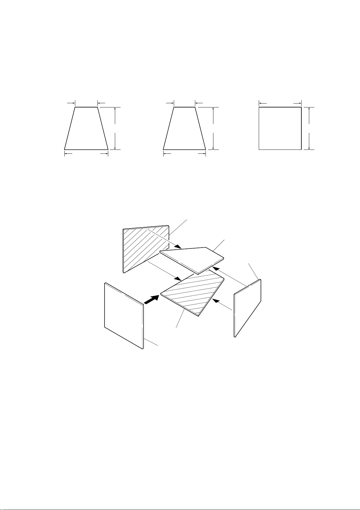
4. Preparing the Flash Adjustment Box
m
A
A dark room is required to provide an accurate strobe adjustment.
If it is not available, prepare the flash adjustment box as gi ven below;
1) Provide woody board A, B and C of 15 mm thickness.
DSC-T1
woody board A (2 sheets)
400 mm
513 mm 513 mm 700 m
woody board B (2 sheets)
370 mm
700 mm730 mm
Fig. 6-1-6.
2) Apply black mat paint to one side of woody board A and B.
3) Attach background paper (J-2501-130-A) to woody board C.
4) Assemble so that the black sides and the background paper side
of woody board A, B and C are internal. (Fig. 6-1-7.)
woody board C (1 sheet)
700 mm
woody board A
woody board B
woody board
woody board B
woody board C
Fig. 6-1-7.
6-7
Page 23
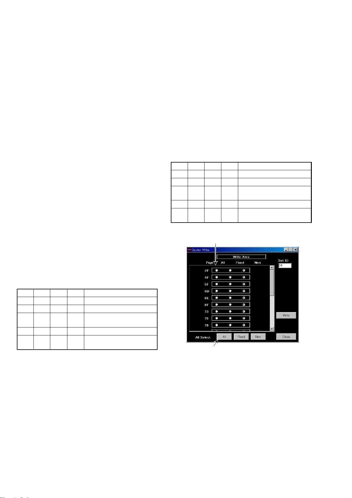
DSC-T1
1-2. INITIALIZATION OF DATA
1-2-1. INITIALIZATION OF DATA
1. Initializing All Pages Data
By performing the following procedure, data of all the pages will
be initialized.
Initializing Method:
1) Select page: 00, address: 01, and set data: 01.
2) Click [Sector Write] on the SEUS screen to display the SEUS
SECTOR WRITE screen.
3) Check that the SET ID is “04”.
4) Click [All] of the ALL SELECT buttons to select all pages.
(Fig. 6-1-8. A)
5) Click [Write] to write the initializing data to the EEPROM of
the camera.
6) Wait for 3 sec.
7) Click [Close] to close the SEUS PAGE EDIT screen.
Modification of 4F, 8E Page Data
If all page data have been initialized, change the data of the “Fixed
data-2” address shown in the following tables by manual input.
1) Select page: 00, address: 01, and set data: 01.
2) Click [Page] on the SEUS screen, and input “4F” or “8E”.
3) Click [Address], and input the “Fixed data-2” address.
4) Click [Set], and input the new data.
Note: New data for changing are not shown in the table because they
are different in destination. When changing the data, copy the
data built in the same model. If copy the data built in the different
model, the camera may not operate.
5) Repeat steps 2 to 4 until all data of the “Fixed data-2” addresses
are changed.
6) Click [Save] to write the changed data to the EEPROM of the
camera.
7) Wait for 3 sec.
2. Initializing Single Page Data
By performing the following procedure, data of the page that you
want to initialize will be initialized.
Initializing Method:
1) Select page: 00, address: 01, and set data: 01.
2) Click [Sector Write] on the SEUS screen to display the SEUS
SECTOR WRITE screen.
3) Check that the SET ID is “04”.
4)
Click [All] of the option buttons of the target page. (Fig. 6-1-8. B)
5) Click [Write] to write the initializing data to the EEPROM of
the camera.
6) Wait for 3 sec.
7) Click [Close] to close the SEUS PAGE EDIT screen.
Note: When 4F page or 8E page is initialized, perform “Modification of
4F, 8E Page Data”. (Refer to “1. Initializing All Pages Data”.)
Processing after Completing Initializing of data
Order Page
Address
Data Procedure
1 20 00 29 Set the data.
2 20 01 29 Set the data.
3 Check “Receive Paket Error” is
displayed on the SEUS screen.
4 Turn on the po wer of the camera.
5 Click [Connect] on the SEUS
screen.
B
Processing after Completing Initializing of data
Order Page
Address
Data Procedure
1 20 00 29 Set the data.
2 20 01 29 Set the data.
3 Check “Receive Paket Error” is
displayed on the SEUS screen.
4 Turn on the po wer of the camera.
5 Click [Connect] on the SEUS
screen.
A
Fig. 6-1-8.
6-8
Page 24

DSC-T1
3. 2F Page Adjustment Address
Address Remark
Initial value
23 80 Test mode
Table. 6-1-2.
4. 4F Page Adjustment Address
Address Remark
46
47
88
94
95
96
97
A1
Initial value
00
00
00
00
Fixed data-2
Fixed data-2
Fixed data-2
Recording counter
(Refer to “Record of Use check” of
“SERVICE MODE”.)
Fixed data-2
Table. 6-1-3.
5. 6E Page Adjustment Address
Address Remark
00
01
02
03
04
05
06
07
08
09
0A
0B
0C
0D
0E
0F
10
11
12
13
14
15
16
17
18
19
1A
1B
1C
1D
1E
1F
20
21
Initial value
00
00
00
00
21
00
0C
00
20
00
0D
00
21
00
0C
00
20
00
0D
00
21
00
0C
00
20
00
0D
00
00
00
00
00
00
00
AWB 5800K standard data input
AWB 3200K standard data input
Address Remark
2A
2D
3A
3D
24
25
26
27
28
29
2B
2C
2E
2F
30
31
32
33
34
35
36
37
38
39
3B
3C
3E
3F
40
41
60
61
62
63
64
65
66
67
72
73
74
75
Initial value
13
00
13
00
13
00
15
00
13
00
13
00
13
00
15
00
13
00
13
00
13
00
15
00
00
00
00
00
00
00
F1
FB
5E
65
F8
06
69
5C
12
00
18
00
AWB 5800K standard data input
Color reproduction adj.
Strobe adj.
Table. 6-1-4.
6-9
Page 25

DSC-T1
6. 6F Page Adjustment Address
Address Remark
10
11
12
13
14
15
16
17
18
19
1A
1B
1C
1D
1E
1F
20
21
22
23
24
25
26
27
28
29
2A
2B
2C
2D
2E
2F
30
31
32
33
34
35
36
37
38
39
3A
3B
3C
3D
3E
3F
40
41
42
43
44
45
46
Initial value
FF
FF
FF
FF
FF
FF
FF
FF
1C
E8
20
A8
1D
88
00
00
00
00
00
00
20
20
80
46
0A
00
00
00
00
00
00
00
00
00
00
00
00
00
00
00
00
00
00
00
00
00
FF
FF
00
00
00
00
00
00
00
AF illumination check
Wide limit adj./Flange back adj.
Flange back adj.
Wide limit adj/
Flange back adj
Flange back adj.
Address Remark
47
48
49
4A
4B
4C
4D
4E
4F
50
51
52
53
60
61
62
63
64
65
66
67
6B
6C
6D
B8
B9
BA
BB
BC
BD
BE
BF
C0
C1
C2
C3
C4
C5
C6
C7
C8
C9
CA
CB
CC
CD
CE
CF
D0
D1
D2
D3
D4
D5
D6
D7
Initial value
00
00
00
00
00
00
00
00
00
00
00
00
00
00
00
00
00
00
30
FE
6D
FF
00
00
10
6B
0F
F6
0F
F7
0F
F2
0F
F7
00
00
00
00
00
30
1B
12
0D
08
80
88
98
90
88
00
00
00
00
00
00
14
Flange back adj.
F No. standard data input
Light value adj.
F No. standard data input/
Mechanical shutter adj.
Mechanical shutter adj.
6-10
Page 26

6F page
Address Remark
DA
DB
DC
DD
DE
DF
EA
EB
EC
ED
D8
D9
E0
E1
E2
E3
E4
E5
E6
E7
E8
E9
EE
EF
Initial value
FF
FF
FF
00
00
00
00
00
00
00
00
00
00
00
00
00
00
00
00
00
00
00
00
00
Strobe adj.
7. 8E Page Adjustment Address
Address Remark
C8 Fixed data-2
Table. 6-1-6.
8. 8F Page Adjustment Address
Address Remark
2A
D0
23
24
25
28
29
2B
2C
Initial value
80
A2
91
80
80
80
80
45
80
VCO adj. (LCD)
V COM adj. (LCD)
Bright adj. (LCD)
White balance adj.(1) (LCD)
White balance adj.(2) (LCD)
White balance adj.(1) (LCD)
White balance adj.(2) (LCD)
Contrast adj. (LCD)
Video output level adj.
Table. 6-1-7.
DSC-T1
Table. 6-1-5.
6-11
Page 27
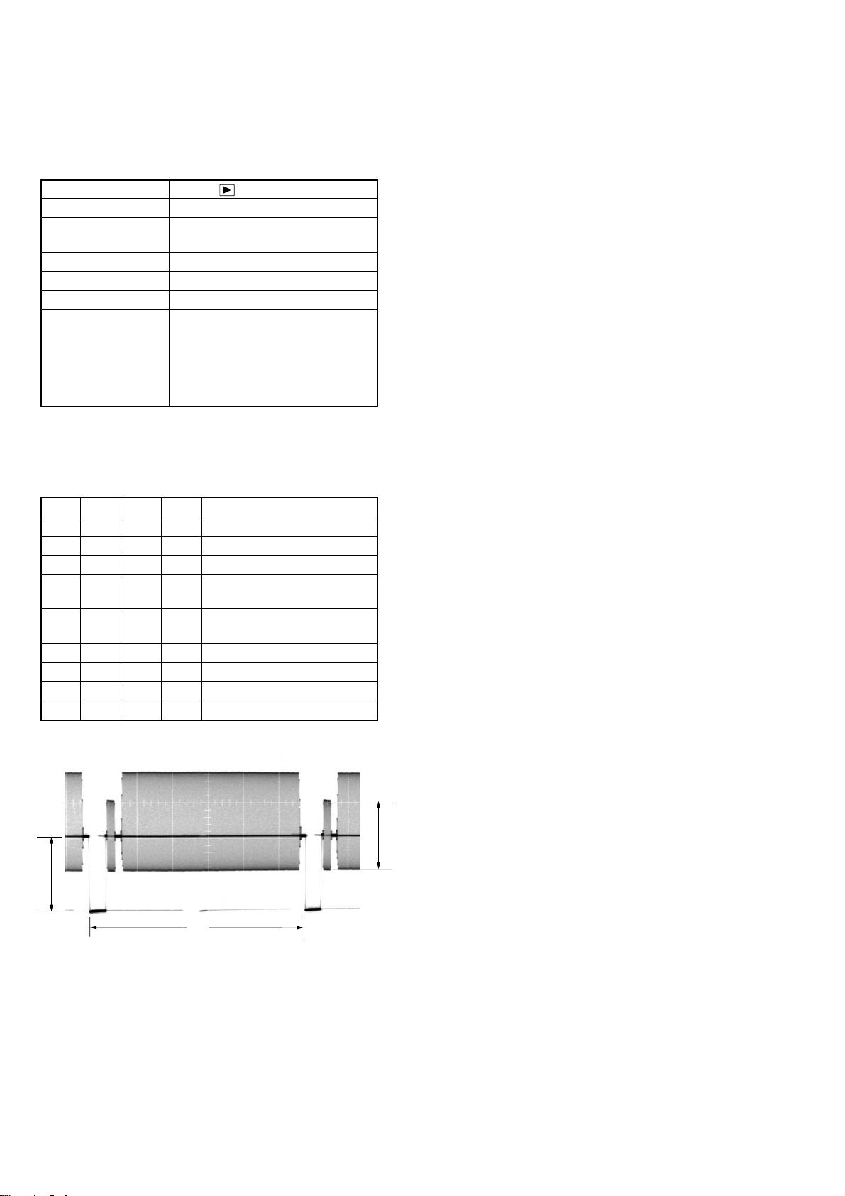
DSC-T1
1-3. VIDEO SYSTEM ADJUSTMENTS
1. Video Output Level Adjustment (SY-95 board)
Adjust the sync level of the composite video signal output.
Mode PLAY ( )
Signal No signal
Measurement Point Video terminal of AV OUT jack
of the cradle (75Ω terminated)
Measuring Instrument Oscilloscope
Adjustment Page 8F
Adjustment Address D0
Specified Value Sync level:
A=286 ± 5mV (NTSC mode)
A=300 ± 5mV (PAL mode)
Burst level:
B=286 ± 30mV (NTSC mode)
B=300 ± 30mV (PAL mode)
Switch setting:
VIDEO OUT (SETUP 2)......................................... (NTSC mode)
............................................ (PAL mode)
Adjusting method:
Order Page
1 00 01 01 Set the data.
260C1
3 80 70 01 Set the data.
4 8F D0 Change the data and set the sync
5 Check that the burst level (B)
6 80 70 00 Write the data.
7 Save the data.
8 Wait for 3 sec.
9 00 01 00 Set the data.
A
Address
Data Procedure
Read the data, and check it is “01”.
level (A) to the specified value.
satisfies the specified value.
B
H
Fig. 6-1-8.
6-12
Page 28

1-4. CAMERA SYSTEM ADJUSTMENTS
Before perform the camera system adjustments, check that the
specified values of “VIDEO SYSTEM ADJUSTMENT” are
satisfied.
1. Data Setting during Camera System Adjustments
Perform the following data setting before the camera system
adjustments.
Note: When the power is turned off, some data settings will be released.
So perform this data setting again when the power is turned off.
Order Page
1 00 01 01 Set the data.
2 4F B7 01 Set the data.
3 2F 23 01 Set the data.
4 60 C1 Read the data, and check it is “02”.
5 80 70 01 Set the data.
6 60 6C 01 Set the data.
7 60 2C 01 Set the data.
Address
Data Procedure
DSC-T1
After completing the camera system adjustments, release the
data setting.
Order Page
1 00 01 01 Set the data.
2 4F B7 00 Set the data.
3 2F 23 80 Set the data.
4 Save the data.
5 Wait for 3 sec.
6 00 01 00 Set the data.
Address
Data Procedure
6-13
Page 29

DSC-T1
2. Wide Limit Adjustment
Adjusted the dispersion of the wide-end of the inner focus lens.
Adjustment Page 6F
Adjustment Address 18, 19
2-1. Adjusting method when the lens device is replaced:
Adjusting method:
Order Page
Address
Data Procedure
1 00 01 01 Set the data.
2 6F 18 Set the data. (Note)
3 6F 19 Set the data. (Note)
4 7C 16 00 Set the data.
5 Save the data.
6 Wait for 3 sec.
7 Perform “Flange Back
Adjustment”.
Note: The data of the addresses 18 and 19, which must be set at Steps 2
and 3, are written on the lens device for service replacement. Four
digits hexadecimal number is written on the lens. Please set the upper
2 digits of the number to the address 18, and set the lower 2 digits to
the address 19.
2-2. Adjusting method when it is not necessary to
replace the lens device and when the SY-95 board
is replaced:
When the data of page: 6F, address: 18 and 19 can be
read from the defective board before replacing it. And
when both of the data are not “00”.
Processing after Completing Adjustments:
Order Page
Address
Data Procedure
1 00 01 01 Set the data.
2 6F 18 Set the read data.
3 6F 19 Set the read data.
4 7C 16 00 Set the data.
5 Save the data.
6 Wait for 3 sec.
7 Perform “Flange Back
Adjustment”.
When the data of page: 6F, address: 18 and 19 can be
read from the defective board before replacing it. And
when both of the data are “00”.
1) Replace the lens device and perform “2-1. Adjusting method when
the lens device is replaced.”
When the data of page: 6F, address: 18 and 19 cannot be
read from the defective board.
1) Replace the lens device and perform “2-1. Adjusting method
when the lens device is replaced.”
Fig.6-1-10.
Note: The data of address 16 of page 7C, set at Step 4 of the adjustment
method of 2-1 and 2-2, is “01” in the state of shipment of the factory.
However, it is “00” when it is adjusted according to the service
manual.
6-14
Page 30

DSC-T1
3. Flange Back Adjustment
The inner focus lens flange back adjustment is carried out
automatically. In whiche v er case, the focus will be de viated during
auto focusing/manual focusing.
Mode STILL ( )
Subject Flange back adjustment jig or
minipattern box (Siemens star chart
with ND filter (Note1))
Measurement Point Data of page: 6F, address: 24, 3E, 3F
Measuring Instrument
Adjustment Page 6F
Adjustment Address 18 to 53
Specified value1 00
Specified value2 0A to 40
Note1: Dark siemens star chart.
Note2: If the data of page: 60, address: 02 is “01”, select page: 60, address:
01, and set data: 00.
Note3: When performing “Flange Back Adjustment”, connect the cables
after disassembling the cradle. Unless the cradle is disassembled,
the USB cable and the power cable will interfere with the flange
back adjustment jig or mini pattern box, and thus the subject cannot
be set correctly.
Preparations for the minipattern box:
1) The minipattern box is installed as shown in the following
figure.
Note: The attachment lenses are not used.
2) Install the minipattern box so that the distance between it and
the front of the lens of the camera is less than 3cm.
3) Make the height of the minipattern box and the camera equal.
4) Check that the output voltage of the regulated power supply is
the specified voltage.
5) Check that at both the zoom lens TELE end and WIDE end,
the center of the siemens star chart and center of the exposure
screen coincide.
Specified voltage:
The specified voltage varies according to the minipattern box, so
adjust the power supply output voltage to the specified voltage
written on the sheet which is supplied with the minipattern box.
Below 3 cm
Minipattern box
Camera
Regulated power supply
Output voltage : Specified voltage ±0.01Vdc
Output current : more than 3.5A
Preparations for the flange back adjustment jig:
1) Install the flange back adjustment jig so that the distance
between it and the front of the lens of the camera is less than
3cm.
2) Adjust the illumination intensity to the chart of the flange back
adjustment jig. (300 to 400 lux)
Data setting when the lens device is replaced:
Note4: Perform this data setting only when the lens device is replaced.
Order Page
Address
Data Procedure
1 00 01 01 Set the data.
2 6F 3E FF Set the data.
Adjusting method:
Order Page
Address
Data Procedure
1 Check that “1. Data Setting
during Camera System
Adjustments” is performed.
2 60 01 13 Set the data.
3 Wait for 1sec.
When the flange back
adjustment jig is used, check
that optimum image is obtained.
4 60 01 27 Set the data.
5 Wait until the movement of the
lens stops.
6 60 02 Read the data, and check it is “01”.
(Note5)
7 6F 3E Read the data, and check it
satisfies the specified value 1.
8 6F 3F Read the data, and check it
satisfies the specified value 1.
9 6F 24 Read the data, and check it
satisfies the specified value 2.
Note5: The adjustment data will be automatically input to page: 6F,
address: 18 to 53
Processing after Completing Adjustments:
Order Page
Address
Data Procedure
1 60 01 00 Set the data.
2 Turn off the power and turn on
again.
3 Perform “Flange Back Check”.
4 If finish the camera system
adjustments, release the data
setting.
(See “1. Data Setting during
Camera System Adjustments”.)
Red (+)
Black (–)
Yellow (SENS +)
White (SENS –)
Black (GND)
Need not connected
Fig.6-1-11.
6-15
Page 31

DSC-T1
4. Flange Back Check
Mode STILL ( )
Subject Siemens star
(1.0 m from the front of the lens)
(Luminance : 200 to 400 lux)
Measurement Point Check operation on TV monitor
(under scan mode)
Measuring Instrument
Specified Value The lens is focused.
Switch setting:
ZOOM ........................................................................... TELE end
MACRO ( ).........................................................................OFF
Checking method:
Order Page
1 Turn off the power and turn on
2 Place the siemens star 1.0 m from
3 Shoot the siemens star with the
4 60 8C 30 Set the data.
5 Observe the TV monitor and
6 60 2C 01 Set the data.
7 Press the ZOOM WIDE button
8 Shoot the Siemens star with the
9 Observe the TV monitor and
Address
Data Procedure
again
the front of the lens.
zoom TELE end.
check that the lens is focused.
and check that zoom operation is
normal.
zoom WIDE end.
check that the lens is focused.
Processing after Completing Adjustments:
Order Page
1 60 8C 00 Set the data.
Address
Data Procedure
6-16
Page 32

5. Picture Frame Setting
E=F
V
EF
Color bar chart picture frame
Effective picture frame
ABC
Mode STILL ( )
Subject Color bar chart and clear chart
(Standard picture frame)
About 30cm (PTB-450) or 12cm
(PTB-1450) from the front of the lens
Measurement Point Video terminal of A/V OUT jack of
the cradle
Measuring Instrument Oscilloscope and TV monitor
Specified Value A=C=B/2, E=F
Switch setting:
ZOOM ........................................................................... WIDE end
MACRO ( ).......................................................................... ON
SCENE (Menu setting)........................................................ AUTO
Setting method:
Order Page
Address
Data Procedure
1 Turn off the power and turn on
again
2 Shoot the color bar chart with
the zoom WIDE end.
3 Adjust the direction and distance
between the pattern box and
camera, and set the picture frame
to the specified position.
4 Perform “1. Data Setting during
Camera System Adjustments”.
5 Remove the color bar chart and
set the clear chart.
6 Check that the whole of the screen
is white. If not, adjust the direction
and distance slightly.
7 10 44 Read the data, and this data named
YH.
8 10 45 Read the data, and this data named
YL.
9 Perform the following
adjustments.
How to reset the zoom and focus when they deviated:
If the zoom and focus deviated due to some reason reset them in the
following method.
Order Page
Address
Data Procedure
1 60 90 00 Set the data.
2 60 91 00 Set the data.
3 60 92 YL Set the data. Note
4 60 93 YH Set the data. Note
5 60 01 79 Set the data.
6 Wait until the movement of the
lens stops.
7 60 07 Read the data, and check it is “01”.
8 60 01 00 Set the data.
Check on an oscilloscope
1. Horizontal period
A
A = C =
B
2
B
C
Fig. 6-1-12.
2. V ertical period
Fig. 6-1-13.
Check on the monitor TV (Underscanned mode)
DSC-T1
Note: YH and YL are the data read in the “Setting method”.
Fig. 6-1-14.
6-17
Page 33

DSC-T1
6. F No. Compensation
Adjusted the dispersion of the iris to every to every F number, and
compensate the exposure.
Mode STILL ( )
Subject Clear chart (Standard picture frame)
Measurement Point Data of page: 6F, address: 6B
Measuring Instrument
Adjustment Page 6F
Adjustment Address 60 to 64, 6B to 6D
Specified value 00
Note1:If the data of page: 60, address: 02 is “01”, select page: 60, address:
01, and set data: 00.
Switch setting:
ZOOM ........................................................................... WIDE end
Adjusting method:
Order Page
Address
Data Procedure
1 Check that “1. Data Setting during
Camera System Adjustments” is
performed.
2 Check the picture frame. If
deviated, perform “5. Picture
Frame Setting”.
3 60 01 BB Set the data.
4 Wait for 15 sec.
5 60 02 Read the data, and check it is “01”.
(Note2)
6 6F 6B Read the data, and check it
satisfies the specified value.
Note2: The adjustment data will be automatically input to page: 6F,
address: 60 to 64, 6B to 6D.
Processing after Completing Adjustments:
Order Page
Address
Data Procedure
1 60 01 00 Set the data.
2 If finish the camera system
adjustments, release the data
setting.
(See “1. Data Setting during
Camera System Adjustments”.)
7. Mechanical Shutter Adjustment
Adjust the dispersion of the opening/closing time and the closing
loss rate of the mechanical shutter. and compensate the exposure.
Mode STILL ( )
Subject Clear chart (Standard picture frame)
Measurement Point Data of page: 6F, address: 6B
Measuring Instrument
Adjustment Page 6F
Adjustment Address 6B to 6D, B8 to D7
Specified value 00
Note1: If the data of page: 60, address: 02 is “01”, select page: 60, address:
01, and set data: 00.
Switch setting:
ZOOM ........................................................................... WIDE end
Adjusting method:
Order Page
Address
Data Procedure
1 Check that “1. Data Setting during
Camera System Adjustments” is
performed.
2 Check the picture frame. If
deviated, perform “5. Picture
Frame Setting”.
3 60 01 AD Set the data.
4 Wait until the movement of the
shutter stops.
5 60 02 Read the data, and check it is “01”.
(Note2)
6 6F 6B Read the data, and check it
satisfies the specified value.
Note2: The adjustment data will be automatically input to page: 6F,
address: 6B to 6D, B8 to D7.
Processing after Completing Adjustments:
Order Page
Address
Data Procedure
1 60 01 00 Set the data.
2 If finish the camera system
adjustments, release the data
setting.
(See “1. Data Setting during
Camera System Adjustments”.)
6-18
Page 34

DSC-T1
8. Light Value Adjustment
Adjust the standard LV value.
Mode STILL ( )
Subject Clear chart (Standard picture frame)
Measurement Point Data of page: 10, address: 0C, 0D
Measuring Instrument Data of page: 6F, address: 65
Adjustment Page 6F
Adjustment Address 65 to 67
Specified value1 0FE0 to 1020
Specified value2 30 to 60
Specified value3 00 to 26
Note1: If the data of page: 60, address: 02 is “01”, select page: 60, address:
Switch setting:
ZOOM ........................................................................... WIDE end
Adjusting method:
01, and set data: 00.
Order Page
1 Check that “1. Data Setting during
2 Check the picture frame. If
3 60 01 0D Set the data.
4 Wait for 2 sec.
5 60 02 Read the data, and check it is “01”.
6 10 0C Read the data, and this data is
7 10 0D Read the data, and this data is
8 Calculate DLV using the
9 Check that DLV satisfies the
10 6F 65 Read the data, and check it
11 60 01 00 Set the data.
12 Wait for 1 sec.
13 60 12 A2 Set the data.
14 60 13 A8 Set the data.
15 60 14 8A Set the data.
16 Wait for 1 sec.
17 10 0C Read the data, and this data is
18 10 0D Read the data, and this data is
19 Calculate DAE using the
20 77 5E 00 Set the data.
21 Wait for 1 sec.
22 10 0C Read the data, and this data is
Address
Data Procedure
Camera System Adjustments” is
performed.
deviated, perform “5. Picture
Frame Setting”.
(Note2)
named D0C.
named D0D.
following equation
(Hexadecimal calculation)
DLV = D0C × 100 + D0D
specified value1.
satisfies the specified value2.
named D0C.
named D0D.
following equation
(Hexadecimal calculation)
DAE = D0C × 100 + D0D
named D0C.
Order Page
23 10 0D Read the data, and this data is
24 Calculate DAE100 using the
25 Check that the difference of DAE
Note2: The adjustment data will be automatically input to page: 6F,
Processing after Completing Adjustments:
Order Page
1 60 01 00 Set the data.
2 60 12 00 Set the data.
3 60 13 00 Set the data.
4 60 14 00 Set the data.
5 77 5E 1E Set the data.
6 Save the data.
7 Wait for 3 sec.
8 Perform next adjustment. If finish
Address
address: 65 to 67.
Address
Data Procedure
named D0D.
following equation
(Hexadecimal calculation)
DAE100 = D0C × 100 + D0D
and DAE100 satisfies the specified
value3. (Hexadecimal).
Data Procedure
the camera system adjustments,
release the data setting. (See “1.
Data Setting during Camera
System Adjustments”.)
6-19
Page 35

DSC-T1
9. Auto White Balance 3200K Standard Data Input
Adjust the white balance standard data at 3200K.
Mode STILL ( )
Subject Clear chart (Standard picture frame)
Measurement Point Data of page: 6E, address: 4F
Measuring Instrument
Adjustment Page 6E
Adjustment Address 04 to 21
Specified value 00
Note1: If the data of page: 60, address: 02 is “01”, select page: 60, address:
01, and set data: 00.
Switch setting:
ZOOM ........................................................................... WIDE end
Adjusting method:
Order Page
Address
Data Procedure
1 Check that “1. Data Setting
during Camera System
Adjustments” is performed.
2 Check the picture frame. If
deviated, perform “5. Picture
Frame Setting”.
3 6E 4F FF Set the data.
4 60 36 01 Set the data.
5 60 01 0B Set the data.
6 Wait for 5 sec.
7 60 02 Read the data, and check it is “01”.
(Note2)
8 6E 4F Read the data, and check it
satisfies the specified value.
Note2: The adjustment data will be automatically input to page: 6E,
address: 04 to 21.
Processing after Completing Adjustments:
Order Page
Address
Data Procedure
1 60 01 00 Set the data.
2 60 36 00 Set the data.
3 Wait for 1 sec.
4 60 37 Read the data, and check it is “00”.
5 Perform “Auto White Balance
5800K Standard Data Input”.
If finish the camera system
adjustments, release the data
setting. (See “1. Data Setting
during Camera System
Adjustments”.)
10.Auto White Balance 5800K Standard Data Input
Adjust the white balance standard data at 5800K.
Mode STILL ( )
Subject Clear chart (Standard picture frame)
Filter Filter C14 for color temperature
correction
Measurement Point Data of page: 6E, address: 4F
Measuring Instrument
Adjustment Page 6E
Adjustment Address 00 to 03, 24 to 41
Specified value 00
Note1: Before perform this adjustment, perform “Auto White Balance
Note2: If the data of page: 60, address: 02 is “01”, select page: 60, address:
3200K Standard Data Input”.
01, and set data: 00.
Switch setting:
ZOOM ........................................................................... WIDE end
Adjusting method:
Order Page
Address
Data Procedure
1 Place the C14 filter for color
temperature correction on the lens.
2 Check that “1. Data Setting during
Camera System Adjustments” is
performed.
3 Check the picture frame. If
deviated, perform “5. Picture
Frame Setting”.
4 6E 00 00 Set the data.
5 6E 01 00 Set the data.
6 6E 02 00 Set the data.
7 6E 03 00 Set the data.
8 6E 4F FF Set the data.
9 60 36 02 Set the data.
10 60 01 A5 Set the data.
11 Wait for 5 sec.
12 60 02 Read the data, and check it is
“01”. (Note3)
13 6E 4F Read the data, and check it
satisfies the specified value.
Note3: The adjustment data will be automatically input to page: 6E,
address: 24 to 41.
Processing after Completing Adjustments:
Order Page
Address
Data Procedure
1 60 01 00 Set the data.
2 60 36 00 Set the data.
3 Wait for 1 sec.
4 60 37 Read the data, and check it is “00”.
5 Perform “Auto White Balance
5800K Check”.
If finish the camera system
adjustments, release the data
setting.
(See “1. Data Setting during
Camera System Adjustments”.)
6-20
Page 36

DSC-T1
11.Auto White Balance 5800K Check
Check that the white balance standard data at 5800K are inputted
properly.
Mode STILL ( )
Subject Clear chart (Standard picture frame)
Filter Filter C14 for color temperature
correction
Measurement Point Data of page: 6E, address: 4F
Measuring Instrument
Specified value 00
Note1: Before perform this adjustment, perform “Auto White Balance
Note2: If the data of page: 60, address: 02 is “01”, select page: 60, address:
5800K Standard Data Input”.
01, and set data: 00.
Switch setting:
ZOOM ........................................................................... WIDE end
Adjusting method:
Order Page
Address
Data Procedure
1 Place the C14 filter for color
temperature correction on the lens.
2 Check that “1. Data Setting during
Camera System Adjustments” is
performed.
3 Check the picture frame. If
deviated, perform “5. Picture
Frame Setting”.
4 6E 4F FF Set the data.
5 60 36 04 Set the data.
6 60 01 3F Set the data.
7 Wait for 10 sec.
8 60 02 Read the data, and check it is “01”.
9 6E 4F Read the data, and check it
satisfies the specified value.
Processing after Completing Adjustments:
Order Page
Address
Data Procedure
1 60 01 00 Set the data.
2 60 36 00 Set the data.
3 Wait for 1 sec.
4 60 37 Read the data, and check it is “00”.
5 Remove the C14 filter.
6 Perform next adjustments.
If finish the camera system
adjustments, release the data
setting.
(See “1. Data Setting during
Camera System Adjustments”.)
12.Auto White Balance 3200K Check
Check that the white balance standard data at 3200K are inputted
properly.
Mode STILL ( )
Subject Clear chart (Standard picture frame)
Measurement Point Data of page: 6E, address: 4F
Measuring Instrument
Specified value 00
Note1: Before perform this adjustment, perform “Auto White Balance
Note2: If the data of page: 60, address: 02 is “01”, select page: 60, address:
3200K Standard Data Input”.
01, and set data: 00.
Switch setting:
ZOOM ........................................................................... WIDE end
Adjusting method:
Order Page
Address
Data Procedure
1 Check that “1. Data Setting during
Camera System Adjustments” is
performed.
2 Check the picture frame. If
deviated, perform “5. Picture
Frame Setting”.
3 6E 4F FF Set the data.
4 60 36 03 Set the data.
5 60 01 0F Set the data.
6 Wait for 10 sec.
7 60 02 Read the data, and check it is “01”.
8 6E 4F Read the data, and check it
satisfies the specified value.
Processing after Completing Adjustments:
Order Page
Address
Data Procedure
1 60 01 00 Set the data.
2 60 36 00 Set the data.
3 Wait for 1 sec.
4 60 37 Check the data, and check it is
“00”.
5 Perform next adjustments.
If finish the camera system
adjustments, release the data
setting.
(See “1. Data Setting during
Camera System Adjustments”.)
6-21
Page 37

DSC-T1
13.CCD Linearity Check
Data picking is done to keep output linearity of the CCD imager,
even if the input level of CCD imager changes.
Mode STILL ( )
Subject Clear chart (Standard picture frame)
Measurement Point
Measuring Instrument
Specified value1 97 to 103 (Note1)
Specified value2 94 to 106 (Note1)
Specified value3 92 to 108 (Note1)
Note1: Decimal number.
Note2: If the data of page: 60, address: 02 is “01”, select page: 60, address:
Note3: For the bit values, refer to “6-2. SERVICE MODE”, “2-2. 2. Bit
Switch setting:
ZOOM ........................................................................... WIDE end
Preparation:
01, and set data: 00.
value discrimination”.
Order Page
1 Check that “1. Data Setting during
2 Check the picture frame. If
3 75 09 Read the data, and memorize it.
4 75 09 04 Set the data.
5 77 F6 Read the data, and memorize it.
6 77 F6 Set Bit2 of the data to “0”. (Note3)
7 77 F7 Read the data, and memorize it.
8 77 F7 Set Bit6 of the data to “1”. (Note3)
9 77 F2 Read the data, and memorize it.
10 77 F2 Set Bit6 of the data to “0”. (Note3)
11 77 F2 Set Bit0 of the data to “0”. (Note3)
12 77 72 Read the data, and memorize it.
13 60 14 90 Set the data.
14 60 12 9F Set the data.
15 60 05 16 Set the data.
16 75 17 Read the data, and memorize it.
17 75 17 50 Set the data.
18 75 18 Read the data, and memorize it.
19 75 18 00 Set the data.
20 75 19 Read the data, and memorize it.
21 75 19 EC Set the data.
22 75 1A Read the data, and memorize it.
23 75 1A 27 Set the data.
24 75 1B Read the data, and memorize it.
25 75 1B 53 Set the data.
26 Wait for 2 sec.
Address
Data of page: 10, address: 80, 81, 82, 83
Data Procedure
Camera System Adjustments” is
performed.
deviated, perform “5. Picture
Frame Setting”.
Checking method:
Order Page
1 Perform “Preparation” before this
2 60 01 F9 Set the data.
3 Wait for 3 sec.
4 60 E1 Read the data, and check it is “08”.
5 10 80 Read the data, and this data is
6 10 81 Read the data, and this data is
7 Calculate DRG0 using the
8 10 82 Read the data, and this data is
9 10 83 Read the data, and this data is
10 Calculate DBG0 using the
11 60 01 00 Set the data.
12 60 E1 00 Set the data.
13 77 72 54 Set the data.
14 Wait for 2 sec.
15 60 01 F9 Set the data.
16 Wait for 3 sec.
17 60 E1 Read the data, and check it is “08”.
18 10 80 Read the data, and this data is
19 10 81 Read the data, and this data is
20 Calculate DRG1 using the
21 10 82 Read the data, and this data is
22 10 83 Read the data, and this data is
23 Calculate DBG1 using the
24 60 01 00 Set the data.
25 60 E1 00 Set the data.
26 77 72 0A Set the data.
27 60 12 A2 Set the data.
28 Wait for 2 sec.
29 60 01 F9 Set the data.
30 Wait for 3 sec.
31 60 E1 Read the data, and check it is “08”.
32 10 80 Read the data, and this data is
33 10 81 Read the data, and this data is
Address
Data Procedure
adjustment.
named D80.
named D81.
following equation
(Hexadecimal calculation)
DRG0 = D80 × 100 + D81
named D82.
named D83.
following equation
(Hexadecimal calculation)
DBG0 = D82 × 100 + D83
named D80.
named D81.
following equation
(Hexadecimal calculation)
DRG1 = D80 × 100 + D81
named D82.
named D83.
following equation
(Hexadecimal calculation)
DBG1 = D82 × 100 + D83
named D80.
named D81.
6-22
Page 38

DSC-T1
Order Page
34 Calculate DRG2 using the
35 10 82 Read the data, and this data is
36 10 83 Read the data, and this data is
37 Calculate DBG2 using the
38 60 01 00 Set the data.
39 60 E1 00 Set the data.
40 77 72 0A Set the data.
41 Wait for 2 sec.
42 60 01 F9 Set the data.
43 Wait for 3 sec.
44 60 E1 Read the data, and check it is “08”.
45 10 80 Read the data, and this data is
46 10 81 Read the data, and this data is
47 Calculate DRG3 using the
48 10 82 Read the data, and this data is
49 10 83 Read the data, and this data is
50 Calculate DBG3 using the
51 Convert DRG0, DBG0, DRG1, DBG1,
52
53 Check that R/G ratio (1) satisfies
54 Check that B/G ratio (1) satisfies
Address
Data Procedure
following equation
(Hexadecimal calculation)
DRG2 = D80 × 100 + D81
named D82.
named D83.
following equation
(Hexadecimal calculation)
DBG2 = D82 × 100 + D83
named D80.
named D81.
following equation
(Hexadecimal calculation)
DRG3 = D80 × 100 + D81
named D82.
named D83.
following equation
(Hexadecimal calculation)
DBG3 = D82 × 100 + D83
DRG2, DBG2, DRG3 and DBG3 to
decimal number, and obtain
DRG0’, DBG0’, DRG1’, DBG1’, DRG2’,
DBG2’, DRG3’ and DBG3’.
Calculate R/G ratio (1), B/G ratio
(1),
R/G ratio (2), B/G ratio (2),
R/G ratio (3) and B/G ratio (3),
using the following equations
(Decimal calculation)
R/G ratio (1) = (DRG1’ / DRG0’) × 100
B/G ratio (1) = (DBG1’ / DBG0’) × 100
R/G ratio (2) = (DRG2’ / DRG0’) × 100
B/G ratio (2) = (DBG2’ / DBG0’) × 100
R/G ratio (3) = (DRG3’ / DRG0’) × 100
B/G ratio (3) = (DBG3’ / DBG0’) × 100
the specified value 1.
(Decimal number)
the specified value 1.
(Decimal number)
Order Page
55 Check that R/G ratio (2) satisfies
56 Check that B/G ratio (2) satisfies
57 Check that R/G ratio (3) satisfies
58 Check that B/G ratio (3) satisfies
Processing after Completing Adjustments:
Order Page
1 60 01 00 Set the data.
2 60 E1 00 Set the data.
3 60 12 00 Set the data.
4 60 14 00 Set the data.
5 75 09 Set the data memorized at
6 77 F6 Set the data memorized at
7 77 F7 Set the data memorized at
8 77 F2 Set the data memorized at
9 77 72 Set the data memorized at
10 60 05 00 Set the data.
11 75 17 Set the data memorized at
12 75 18 Set the data memorized at
13 75 19 Set the data memorized at
14 75 1A Set the data memorized at
15 75 1B Set the data memorized at
16 Save the data.
17 Wait for 3 sec.
18 Perform next adjustments.
Address
Address
Data Procedure
Linearity check of low
luminance
the specified value 2.
(Decimal number)
the specified value 2.
(Decimal number)
Linearity check of very low
luminance
the specified value 3.
(Decimal number)
the specified value 3.
(Decimal number)
Data Procedure
“Preparation”.
“Preparation”.
“Preparation”.
“Preparation”.
“Preparation”.
“Preparation”.
“Preparation”.
“Preparation”.
“Preparation”.
“Preparation”.
If finish the camera system
adjustments, release the data
setting.
(See “1. Data Setting during
Camera System Adjustments”.)
6-23
Page 39

DSC-T1
14.Color Reproduction Adjustment
Adjust the color reproduction of yellow, red, blue and cyan so that
proper color reproduction is produced.
Mode STILL ( )
Subject Color bar chart
(Standard picture frame)
Measurement Point Video terminal of A/V OUT jack of
the cradle
Measuring Instrument NTSC vectorscope
Adjustment Page 6E
Adjustment Address 60 to 67
Specified value 1 Data of page: 6E, address: 4F is “00”
Specified value 2 Each center of all color luminance
points should settle within each color
reproduction frame.
Note1: If the data of page: 60, address: 02 is “01”, select page: 60, address:
Switch setting:
Adjusting method:
01, and set data: 00.
ZOOM....................................................................WIDE end
VIDEO OUT (SET UP of Menu) ................................. NTSC
Order Page
1 Install the color bar chart.
2 Check that “1. Data Setting during
3 Check the picture frame. If
4 7A 00 Read the data, and this data is
5 7A 00 00 Set the data.
6 6E 4F FF Set the data.
7 60 01 AB Set the data.
8 Wait for 1 sec.
9 60 01 A9 Set the data.
10 Wait until the color of the screen
11 60 02 Read the data, and check it is “01”.
12 6E 4F Read the data, and check it
13 Adjust the GAIN and PHASE of
14 Check that each center of all color
Address
Data Procedure
Camera System Adjustments” is
performed.
deviated, perform “5. Picture
Frame Setting”.
named D00.
stops changing.
(Note2)
satisfies the specified value 1.
the vectorscope so that the burst
luminance point is set at the
specified position.
luminance points is set in each
color reproduction frame.
Processing after Completing Adjustments:
Order Page
1 60 01 00 Set the data.
2 7A 00 Set the data memorized at
3 Save the data.
4 Wait for 3 sec.
5 Perform “Color Reproduction
Burst position
Address
Data Procedure
“Adjusting method”.
Check”. If finish the camera
system adjustments, release the
data setting.
(See “1. Data Setting during
Camera System Adjustments”.)
Fig. 6-1-15.
Note2: The adjustment data will be automatically input to page: 6E,
address: 60 to 67.
6-24
Page 40

DSC-T1
15.CCD White Defect Compensation Check
The positions of the white defective pixel are detected, and check
that the pixels can be corrected.
Mode STILL ( )
Subject Clear chart (Standard picture frame)
Measurement Point Data of page: 60, address: 55
Measuring Instrument
Specified value 1 00 to 40
Specified value 2 00
Note: If the data of page: 60, address: 02 is “01”, select page: 60, address:
01, and set data: 00.
Switch setting:
ZOOM ........................................................................... WIDE end
Adjusting method:
Order Page
1 Install the clear chart.
2 Check that “1. Data Setting during
3 Check the picture frame. If
4 7D 64 Read the data, and memorize the
5 7D 64 1E Set the data.
6 7D 69 Read the data, and memorize the
7 7D 69 28 Set the data.
8 60 01 8B Set the data.
9 Wait for 30sec.
10 60 02 Read the data, and check it is “01”.
11 60 55 Read the data, and check it
12 60 01 00 Set the data.
13 Wait for 1sec.
14 7D 64 0F Set the data.
15 7D 69 C0 Set the data.
16 60 01 87 Set the data.
17 Wait for 30sec.
18 60 02 Read the data, and check it is “01”.
19 60 55 Read the data, and check it
Address
Data Procedure
Camera System Adjustments” is
performed.
deviated, perform “5. Picture
Frame Setting”.
data.
data.
satisfies the specified value 1.
satisfies the specified value 2.
Processing after Completing Adjustments:
Order Page
1 60 01 00 Set the data.
2 7D 64 Set the data memorized at
3 7D 69 Set the data memorized at
4 Save the data.
5 Wait for 3 sec.
6 Perform next adjustments.
Address
Data Procedure
“Adjusting method”.
“Adjusting method”.
If finish the camera system
adjustments, release the data
setting.
(See “1. Data Setting during
Camera System Adjustments”.)
6-25
Page 41

DSC-T1
16.CCD Black Defect Compensation Check
The positions of the black defective pixel are detected, and check
that the pixels can be corrected. And conf irms that there is no trash
in the surface of the CCD imager, the optical f ilter and the inside of
the lens.
Mode STILL ( )
Subject Clear chart (Standard picture frame)
Measurement Point Data of page: 60, address: 55
Measuring Instrument
Specified value 1 00 to 30
Specified value 2 00
Note1: Check that there are no dust, no dirt and no reflection on the clear
Note2: If the data of page: 60, address: 02 is “01”, select page: 60, address:
Adjusting method:
chart.
01, and set data: 00.
Order Page
1 Check that “1. Data Setting during
2 Check the picture frame. If
3 7D 65 Read the data, and memorize the
4 7D 65 0A Set the data.
5 60 90 00 Set the data.
6 60 91 03 Set the data.
7 60 92 00 Set the data.
8 60 93 00 Set the data.
9 60 01 79 Set the data.
10 60 30 08 Set the data.
11 60 07 Read the data, and check it is “01”.
12 Check that the whole of the screen
13 60 01 8D Set the data.
14 Wait for 30 sec.
15 60 02 Read the data, and check it is “01”.
16 60 55 Read the data, and check it
17 60 01 00 Set the data.
18 Wait for 1 sec.
19 7D 65 0E Set the data.
20 60 01 89 Set the data.
21 Wait for 30 sec.
22 60 02 Read the data, and check it is “01”.
23 60 55 Read the data, and check it
Address
Data Procedure
Camera System Adjustments” is
performed.
deviated, perform “5. Picture
Frame Setting”.
data.
is white.
satisfies the specified value 1.
If the data is “00”, proceed to
“Processing after Completing
Adjustments”
satisfies the specified value 2.
Processing after Completing Adjustments:
Order Page
1 60 01 00 Set the data.
2 Wait for 1 sec.
3 60 2C 00 Set the data.
4 60 30 00 Set the data.
5 60 91 00 Set the data.
6 7D 65 Set the data memorized at
7 Save the data.
8 Wait for 3 sec.
9 Perform next adjustments.
Address
Data Procedure
“Adjusting method”.
If finish the camera system
adjustments, release the data
setting.
(See “1. Data Setting during
Camera System Adjustments”.)
6-26
Page 42
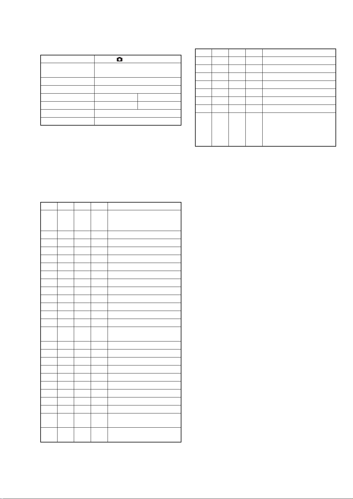
DSC-T1
17.Strobe Adjustment
Adjust the light level and white balance when the strobe light flashes.
Mode STILL ( )
Subject Background paper (J-2501-130-A)
(50cm from the front of the lens)
Measurement Point
Data of page 6F, address: DC
Measuring Instrument Data of page 6E, address: 4F
Adjustment Page 6F 6E
Adjustment Address D8 to EF 72 to 75
Specified Value1 03 to 09
Specified Value2 00
Note1: Perform this adjustment in the dark room or use the flash
Note2: Any light other than the strobe light should not light up the plate.
Note3: After the power is turned on, this adjustment can be done only
Note4: If the data of page: 60, address: 02 is “01”, select page: 60, address:
adjustment box.
once.
01, and set data: 00.
Switch setting:
ZOOM ........................................................................... WIDE end
Adjusting method:
Order Page
Address
Data Procedure
1 Check that “1. Data Setting
during Camera System
Adjustments” is performed.
2 60 2C 01 Set the data.
3 60 90 00 Set the data.
4 60 91 00 Set the data.
5 60 92 FF Set the data.
6 60 93 FF Set the data.
7 60 6C 01 Set the data.
8 60 01 79 Set the data.
9 Wait for 5 sec.
10 60 07 Read the data, and check it is “01”.
11 6E 4F FF Set the data.
12 60 01 B9 Set the data.
13 Check the flashing.
14 60 02 Read the data, and check it is “01”.
(Note5)
15 6F D8 Read the data, and check it is “00”.
16 60 01 00 Set the data.
17 Wait for 5 sec.
18 60 ED Read the data, and check it is “02”.
19 Wait for 1 sec.
20 60 01 E7 Set the data.
21 Check the flashing.
22 60 02 Read the data, and check it is “01”.
23 6F D8 Read the data, and check it is “00”.
24 6F DC Read the data, and check it
satisfies the specified value 1.
25 6E 4F Read the data, and check it
satisfies the specified value 2.
Processing after Completing Adjustments:
Order Page
Address
Data Procedure
1 60 01 00 Set the data.
2 60 2C 00 Set the data.
3 60 6C 00 Set the data.
4 60 90 00 Set the data.
5 60 91 00 Set the data.
6 60 92 00 Set the data.
7 60 93 00 Set the data.
8 If finish the camera system
adjustments, release the data
setting.
(See “1. Data Setting during
Camera System Adjustments”.)
Note5: The adjustment data will be automatically input to page: 6F,
address: D8 to EF and to page: 6E, address: 72 to 75.
6-27
Page 43

DSC-T1
18.Auto Focus Illumination Check
Check the auto focus illumination optical axis.
Mode STILL ( )
Subject Background paper (J-2501-130-A).
(50cm from the front of the lens)
Measurement Point Monitor TV (under scan mode)
Measuring Instrument
Adjustment Page 6F
Adjustment Address 10 to 17
Specified Value 1 Center of luminance point should
settle within the specified frame.
Specified Value 2 Data of page: 6F, address: 10 is “00”.
Note1: Perform this adjustment in the dark room or use the flash
Note2: Any light other than the strobe light should not light up the plate.
Note3: If the data of page: 60, address: 02 is “01”, select page: 60, address:
adjustment box.
01, and write data: 00.
Switch setting:
SCENE (Menu) ................................................................... AUTO
Preparations:
1) Take a copy of the AF illumination axis frame with a clear
sheet. (Enlarge the frame in same size as the effective picture
frame of the monitor TV.)
Adjusting method:
Order Page
Address
Data Procedure
1 Turn off the power and turn on
again
2 00 01 01 Set the data.
3 AF 90 Read the data, and memorize it.
4 AF 90 Decrease the data from “5F”, and
stop it when the black frame just
appears on the monitor TV screen.
5 Attach the copied AF illumination
axis frame (transparent) on the
monitor TV screen. (The frame of
the AF illumination axis frame
and the gray frame of the monitor
TV screen must be agree.)
6 7B A9 06 Set the data.
7 60 01 EF Set the data.
8 Check that the AF illumination is
lit.
9 60 02 Read the data, and check it is “01”.
(Note4)
10 Check that center of the luminance
spot is set in the specified frame
of the AF illumination axis frame.
11 6F 10 Read the data, and check it
satisfies the specified value 2.
Fig. 6-1-16.
Processing after Completing Adjustments:
Order Page
Address
Data Procedure
1 60 01 00 Set the data.
2 AF 90 Set the data memorized at
“Adjusting method”.
3 Save the data.
4 Wait for 3 sec.
5 If finish the camera system
adjustments, release the data
setting.
(See “1. Data Setting during
Camera System Adjustments”.)
Note4: The adjustment data will be automatically input to page: 6F,
address: 10 to 17.
6-28
Page 44
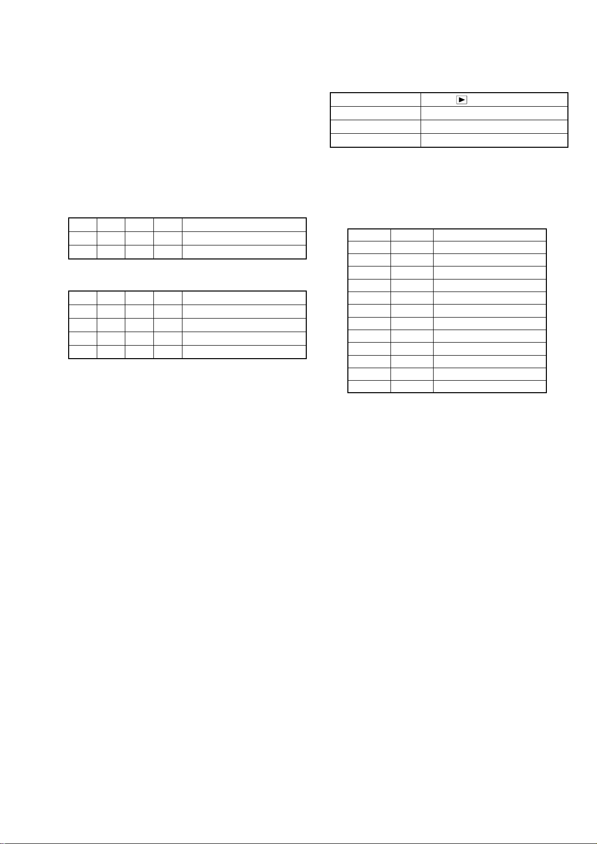
DSC-T1
1-5. LCD SYSTEM ADJUSTMENT
Note: When replacing the LCD unit, be careful to prev ent damages caused
by static electricity.
Switch setting:
LCD ON/OFF ........................................................................... ON
1. Data Setting during LCD System Adjustments
Perform the following data setting before the LCD system
adjustments.
Note: When the power is turned off, some data settings will be released.
So perform this data setting again when the power is turned off.
Order Page
1 00 01 01 Set the data.
2 80 70 01 Set the data.
After completing the LCD system adjustments, release the data
setting.
Order Page
1 80 70 00 Set the data.
2 Save the data.
3 Wait for 3 sec.
4 00 01 00 Set the data.
Address
Address
Data Procedure
Data Procedure
2. LCD Initial Data Input (1)
Mode PLAY ( )
Signal Arbitrary
Adjustment Page 8F
Adjustment Address 20, 21, 23 to 2C
Adjusting method:
1) Select page: 00, address: 01, and set data: 01.
2) Select page: 8F, and set the data in the following table.
3) Save the data.
4) Wait for 3 sec.
5) Select page: 00, address: 01, and set data: 00.
Address
20
21
23
24
25
26
27
28
29
2A
2B
2C
Data
89
B8
B0
A2
91
3F
41
80
95
80
95
60
Remark
Fixed data
Fixed data
VCO adj.
Fixed data
Bright adj.
Fixed data
Fixed data
White balance adj. (1)
White balance adj. (2)
White balance adj. (1)
White balance adj. (2)
Contrast adj.
6-29
Page 45

DSC-T1
3. VCO Adjustment (SY-95 board)
Set the VCO free-run frequency. If deviated, the LCD screen will
be blurred.
Mode PLAY ( )
Subject Arbitrary
Measurement Point Data of page: 80, address: 02
Measuring Instrument
Adjustment Page 8F
Adjustment Address 23
Specified Value 01
Note1: A memory stick DUO must be inserted.
Adjusting method:
Order Page
Address
Data Procedure
1 Check that “1. Data Setting during
LCD System Adjustments” is
performed.
2 8F 34 32 Set the data.
3 80 00 00 Set the data.
4 80 01 00 Set the data.
5 80 00 01 Set the data.
6 Wait for 1 sec.
7 80 02 Read the data, and check it is “01”.
(Note2)
8 Wait for 1 sec.
9 If finish the LCD system
adjustments, release the data
setting.
(See “1. Data Setting during
LCD System Adjustments”.)
Note2: If the data is other than “01”, adjustment has errors. See the
following table.
Data of page: 80, Contents of adjustment error
address: 02
01 Normally finished
10 Reached an upper limit
20 Reached a lower limit
30 Time out
40 Out of adjustment range
50 Adjustment is impossible
4. Bright Adjustment (SY-95 board)
Set the level of the VIDEO signal for driving the LCD to the specified
value. If deviated, the screen image will be blackish or saturated
(whitish).
Mode PLAY ( )
Subject Arbitrary
Measurement Point Data of page: 80, address: 02
Measuring Instrument
Adjustment Page 8F
Adjustment Address 25
Specified Value 01
Note1: A memory stick DUO must be inserted.
Adjusting method:
Order Page
Address
Data Procedure
1 Check that “1. Data Setting during
LCD System Adjustments” is
performed.
2 8F 38 A8 Set the data.
3 80 00 00 Set the data.
4 80 01 00 Set the data.
5 80 00 03 Set the data.
6 Wait for 1 sec.
7 80 02 Read the data, and check it is “01”.
(Note2)
8 Wait for 1 sec.
9 If finish the LCD system
adjustments, release the data
setting.
(See “1. Data Setting during
LCD System Adjustments”.)
Note2: If the data is other than “01”, adjustment has errors. See the
following table.
Data of page: 80, Contents of adjustment error
address: 02
01 Normally finished
10 Reached an upper limit
20 Reached a lower limit
30 Time out
40 Out of adjustment range
50 Adjustment is impossible
6-30
Page 46
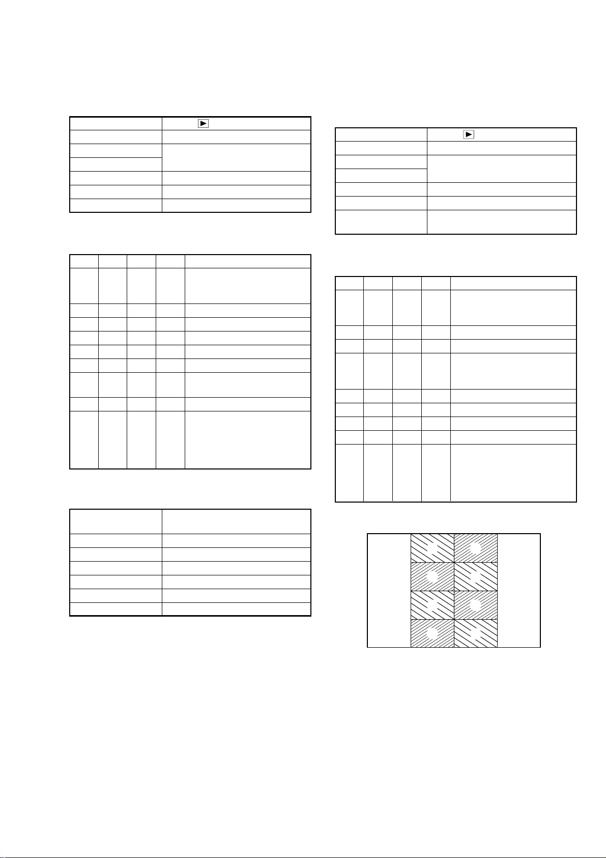
DSC-T1
5. Contrast Adjustment (SY-95 board)
Set the level of the VIDEO signal for driving the LCD to the specified
value. If deviated, the screen image will be blackish or saturated
(whitish).
Mode PLAY ( )
Subject Arbitrary
Measurement Point Data of page: 80, address: 02
Measuring Instrument
Adjustment Page 8F
Adjustment Address 2C
Specified Value 01
Note1: A memory stick DUO must be inserted.
Adjusting method:
Order Page
Address
Data Procedure
1 Check that “1. Data Setting during
LCD System Adjustments” is
performed.
2 8F 39 28 Set the data.
3 80 00 00 Set the data.
4 80 01 00 Set the data.
5 80 00 05 Set the data.
6 Wait for 1 sec.
7 80 02 Read the data, and check it is “01”.
(Note2)
8 Wait for 1 sec.
9 If finish the LCD system
adjustments, release the data
setting.
(See “1. Data Setting during
LCD System Adjustments”.)
Note2: If the data is other than “01”, adjustment has errors. See the
following table.
6. V COM Adjustment (SY-95 board)
Set the DC bias of the common electrode drive signal of LCD to the
specified value.
If deviated, the LCD display will move, producing flicker and
conspicuous vertical lines.
Mode PLAY ( )
Subject Arbitrary
Measurement Point Check on LCD display
Measuring Instrument
Adjustment Page 8F
Adjustment Address 24
Specified Value The brightness difference between the
section A and section B is minimum.
Note: A memory stick DUO must be inserted.
Adjusting method:
Order Page
Address
Data Procedure
1 Check that “1. Data Setting during
LCD System Adjustments” is
performed.
2 80 71 76 Set the data.
3 8F 41 23 Set the data.
4 8F 24 Change the data so that the
brightness of the section A and
that of the section B is equal.
5 80 71 FF Set the data.
6 8F 41 21 Set the data.
7 Save the data.
8 Wait for 3 sec.
9 If finish the LCD system
adjustments, release the data
setting.
(See “1. Data Setting during
LCD System Adjustments”.)
Data of page: 80, Contents of adjustment error
address: 02
01 Normally finished
10 Reached an upper limit
20 Reached a lower limit
30 Time out
40 Out of adjustment range
50 Adjustment is impossible
B
A
B
A
Fig. 6-1-17.
A
B
A
B
6-31
Page 47

DSC-T1
7. White Balance Adjustment (1) (SY-95 board)
Correct the white balance of the transmissive mode.
If deviated, the LCD screen color cannot be reproduced.
Mode PLAY ( )
Subject Arbitrary
Measurement Point Check on LCD display
Measuring Instrument
Adjustment Page 8F
Adjustment Address 28, 2A
Specified Value The LCD screen should not be colored.
Note1: A memory stick DUO must be inserted.
Note2: Check the white balance only when replacing the following parts.
If necessary, adjust them.
1. LCD panel
2. Light induction plate
3. IC803 of MS-148 board.
Adjusting method:
Order Page
Address
Data Procedure
1 Check that “1. Data Setting during
LCD System Adjustments” is
performed.
2 80 71 52 Set the data.
3 80 84 02 Set the data.
4 8F 28 80 Set the data.
5 8F 2A 80 Set the data.
6 8F 28 Check that the LCD screen is not
colored. If not colored, proceed to
step 10.
7 8F 28 Change the data so that the LCD
screen is not colored.
8 8F 2A Change the data so that the LCD
screen is not colored.
9 8F 2A If the LCD screen is colored,
repeat steps 7 to 9.
10 80 71 FF Set the data.
11 Save the data.
12 Wait for 3 sec.
13 If finish the LCD system
adjustments, release the data
setting.
(See “1. Data Setting during
LCD System Adjustments”.)
8. White Balance Adjustment (2) (SY-95 board)
Correct the white balance of the reflective mode.
If deviated, the LCD screen color cannot be reproduced.
Mode PLAY ( )
Subject Arbitrary
Measurement Point Data of page: 80, address: 02
Measuring Instrument
Adjustment Page 8F
Adjustment Address 29, 2B
Specified Value 01
Note1: A memory stick DUO must be inserted.
Adjusting method:
Order Page
Address
Data Procedure
1 Check that “1. Data Setting during
LCD System Adjustments” is
performed.
2 80 83 00 Set the data.
3 80 71 43 Set the data.
4 8F 3A 6C Set the data.
5 80 00 00 Set the data.
6 80 01 00 Set the data.
7 80 00 09 Set the data.
8 Wait for 1 sec.
9 80 02 Read the data, and check it is “01”.
(Note2)
10 Wait for 1 sec.
11 8F 3B 71 Set the data.
12 80 00 00 Set the data.
13 80 01 01 Set the data.
14 80 00 09 Set the data.
15 Wait for 1 sec.
16 80 02 Read the data, and check it is “01”.
(Note2)
17 Wait for 1 sec.
18 80 83 01 Set the data.
19 80 71 FF Set the data.
20 If finish the LCD system
adjustments, release the data
setting.
(See “1. Data Setting during
LCD System Adjustments”.)
Note2: If the data is other than “01”, adjustment has errors. See the
following table.
Data of page: 80, Contents of adjustment error
address: 02
01 Normally finished
10 Reached an upper limit
20 Reached a lower limit
30 Time out
40 Out of adjustment range
50 Adjustment is impossible
6-32
Page 48

DSC-T1
6-2. SERVICE MODE
2-1. APPLICATION FOR ADJUSTMENT (SEUS)
The application for adjustment (SEUS) is used for changing the
calculation coefficient in signal processing, EVR data, etc. The SEUS
performs bi-directional communication between the personal
computer (PC) and the unit using the USB signal. The resultant
data of this bi-directional communication is written in the nonvolatile memory.
2-1-1. Using Method of SEUS
1. Connection
1) Connect the HASP key to the USB port of the PC.
2) Connect the camera to another USB port of the PC.
3) Insert a memory stick DUO to the camera.
4) Confirm that the camera starts in the USB mode.
5) Start the SEUS on the PC.
6) Click [Connect] on the SEUS screen. If the connection is
normal, the SEUS screen will be as shown in Fig. 6-2-1,
indicating the “connected” state.
Note: The SEUS will go in “disconnect” state, if the camera is turned
off (for instance, by resetting the unit). In such a case, click
[Connect] on the SEUS screen to restore the “connected” state.
2. Operation
• Page change
To change the page, click [Page] on the SEUS screen and enter
the page to be changed. The page is displayed in hexadecimal
notation.
• Address change
T o change the address, click [Address] on the SEUS screen and
enter the address to be changed. Or click [ B ] to increase the
address, click [ b ] to decrease the address. The address is
displayed in hexadecimal notation.
• Data change
T o change the data, click [Set] on the SEUS screen and enter the
data. Or click [ v ] to increase the data, click [ V ] to decrease
the data. The data is displayed in hexadecimal notation.
This operation does not write the data to the nonvolatile memory .
If you want to write the changed data, click [Save] to write it.
• Data saving
T o write the all changed data to the nonvolatile memory ,
click [Save] on the SEUS screen and wait for 3 sec.
• Data reading
The data displayed on the SEUS screen are the data values at the
time when the pages and addresses were set, and they are not
updated automatically. To check the data change, click [Read]
on the SEUS screen and update the displayed data.
Fig. 6-2-1.
2-1-2. Precaution on Use of SEUS
Mishandling of the SEUS may erase the correct adjustment data at
times. To prevent this, it is recommended that all adjustment data
be saved before beginning adjustments.
1) Click [Page Edit] on the SEUS screen.
2) Click [Page], and enter the page number to be saved.
3) Click [Read] to read the data to be saved from the camera.
4) Click [File] and save the data to the PC.
6-33
Page 49

DSC-T1
2-2. SERVICE MODE
1. Setting the Test Mode
Page 2F Address 23
Data Function
80 Normal
01 Forced STILL mode power ON
02 Forced PLAY mode power ON
00 Forced MOVIE mode power ON
• Before setting the data, select page: 00, address: 01, and set data:
01.
• For page 2F, the data set is recorded in the non-volatile memory
by saving data. In this case, take note that the test mode will not
be exited even when the main power is turned off.
• After completing adjustments/repairs, release the data setting .
1) Select page: 00, address: 01, and set data: 01.
2) Select page: 2F, address: 23, and set data: 80.
3) Save the data.
4) Wait for 3 sec.
5) Select page: 00, address: 01, and set data: 00.
2. Bit value discrimination
Bit values must be discriminated using the hexadecimal data for
following items. Use the table below to discriminate if the bit v alue
is “1” or “0”.
Hexadecimal data
bit3 to bit0 discrimination
bit7 to bit4 discrimination
Display on the
adjustment
remote
commander
A
A (A)
B (b)
C (c)
D (d)
B
E (E)
F (F)
bit3
or
bit7
0
1
2
3
4
5
6
7
8
9
0
0
0
0
0
0
0
0
1
1
1
1
1
1
1
1
Bit values
bit2
or
bit6
0
0
0
0
1
1
1
1
0
0
0
0
1
1
1
1
bit1
or
bit5
0
0
1
1
0
0
1
1
0
0
1
1
0
0
1
1
bit0
or
bit4
0
1
0
1
0
1
0
1
0
1
0
1
0
1
0
1
Examples: If the hexadecimal data is “8E”, the bit values for bit7 to bit4
are shown in the A column, and the bit values for bit3 to bit0
are shown in the B column.
6-34
Page 50

3. Switch check (1)
Page 20 Address 80
DSC-T1
Bit
POWER switch (XPWER ON)
0
(Control switch block S001)
Lens cover open switch (XLENS CAP ON)
2
(SY-95 board S401)
Function
When bit value=1
OFF
Closed
When bit value=0
ON
Open
Using method:
1) Select page: 20, address: 80.
2) Read the data. By discriminating the bit value of the data, the state of the switches can be discriminated.
4. Switch check (2)
Page 20 Address 90 to 92, 95
Using method:
1) Select page: 20, address: 90 to 92, 95.
2) Read the data. By discriminating the data, the pressed key can be discriminated.
Address
90
(MODE AD0)
(IC491 J6 )
91
(KEY AD1)
(IC491
H6
)
92
(KEY AD2)
(IC491
G6
)
95
(MODE DIAL0)
(IC491
J8
)
00 to 0B
MENU
(Control switch block)
(S007)
Control button UP
(Control switch block)
(S006)
WIDE
(Control switch block)
(S003)
Mode switch MOVIE
(MS-148 board)
(S101)
0C to 26
Control button LEFT
(Control switch block)
(S005)
IMAGE SIZE/DELETE
(Control switch block)
(S009)
TELE
(Control switch block)
(S004)
Mode switch STILL
(MS-148 board)
(S101)
Data
27 to 47
DISPLAY/LCD BACK LIGHT
(Control switch block)
(S013)
Control button RIGHT
(Control switch block)
(S010)
Mode switch PLAY
(MS-148 board)
(S101)
48 to 72
Control button DOWN
(Control switch block)
(S011)
Control button SET
(Control switch block)
(S008)
73 to FF
No key input
No key input
No key input
5. Switch check (3)
Page 80 Address 13
Function
Shutter button (XAE LOCK SW)
When data = 00
Off
When data = 01
On
When data = 02
On
(Control switch block S002)
Shutter button (XSHTR ON SW)
Off
Off
On
(Control switch block S002)
Using method:
1) Select page: 80, address: 13.
2) Read the data. By discriminating the data, the state of the switches can be discriminated.
6-35
Page 51

DSC-T1
6. LED check
Page 20 Address 04
Page 80 Address 12
Page 8E Address FE
Using method:
1) Select page: 00, address: 01, set data: 01.
2) Select page: 8E, address: FE, set data: 20.
3) Select page: 80, address: 12, set data: 01.
4) Select page: 20, address: 04, set data: 02.
5) Check that all LED (Power, Flash/Charge, MS access, AF illmination) are lit.
6) Select page: 20, address: 04, set data: 00.
7) Select page: 80, address: 12, set data: 00.
8) Select page: 8E, address: FE, set data: 00.
9) Select page: 00, address: 01, set data: 00.
7. Record of Use check
Page 4F Address 94 to 97
Address
94
95
96
97
Using method:
1) The recording counter data is displayed at page: 4F, addresses: 94 to 97. These data are named D94, D95, D96 and D97 respectively.
2) Calculate the recording counter (N) using following equation. (Hexadecimal calculation)
N = D97 + D96 × 100 + D95 × 10000 + D94 × 1000000
8. Self Diagnostics Log check
Page 20 Address B0 to B8
Address
B0
B1
B2
B3
B4
B5
B6
B7
B8
Function
Recording counter
(Hexadecimal)
Initial value
00
00
00
00
00
00
00
00
00
“Repaired by” code (Occurred 1st time) *1
“Block function” code (Occurred 1st time)
“Detailed” code (Occurred 1st time)
“Repaired by” code (Occurred 2nd time) *1
“Block function” code (Occurred 2nd time)
“Detailed” code (Occurred 2nd time)
“Repaired by” code (Occurred 3rd time) *1
“Block function” code (Occurred 3rd time)
“Detailed” code (Occurred 3rd time)
Remarks
1000000-digit and 1000000-digit
1000000-digit and 10000-digit
1000-digit and 100-digit
10-digit and 1-digit
Function
*1: “C” t “01”, “E” t “03”
Using method:
1) The self diagnostics log is displayed at page: 20, addresses: B0 to B5.
Note: These data will be erased when the lithium battery (CN-198 board) is removed.
6-36
Page 52

DSC-T1
〈FOR CAMERA COLOR REPRODUCTION ADJUSTMENT〉
〈AF ILLUMINATION FRAME〉
T ake a copy of CAMERA COLOR
REPRODUCTION FRAME with
a clear sheet for use.
✂
6-38E
✂
Page 53

1. Before starting adjustment
EVR Data Re-writing Procedure When Replacing Board
The data that is stored in the repair board, is not necessarily correct.
Perform either procedure 1 or procedure 2 or procedure 3 when replacing board.
Procedure 1
Save the EVR data of the machine in which a board is going to be replaced. Download the saved data after a
board is replaced.
(Machine before starting repair)
SECTION 6
ADJUSTMENTS
PC PC
DSC-T1
(Machine after a board is replaced)
Save the EVR data
to a personal computer.
Download the saved
data to a machine.
Procedure 2
Remove the flash memory from the board of the machine that is going to be repaired. Install the removed
flash memory to the replaced board.
Remove the flash memory and install it.
(Former board)
(New board)
Procedure 3
When the data cannot be saved due to defectiv e flash memory , or when the flash memory cannot be r emoved
or installed, save the data from the same model of the same destination, and download it.
(Machine to be repaired) (Machine to be repaired)
PC
Save the data.
(The same model of the same destination)
After the EVR data is saved and downloaded, check the
respective items of the EVR data.
(Refer to page 6-2 for the items to be checked.)
Download the data.
6-1
Page 54

DSC-T1
1-1. Adjusting items when replacing main parts and boards
When replacing main parts and boards, adjust the items indicated by z in the following table.
Note: The automatic Adjustment Program does not support the “Initialization of data” and “Wide Limit Adjustment”. Perform them
manually.
Replaced parts
Block Mounted parts Board
replacement replacement replacement
Flash memory
replacement
Adjusting item Adjustment
(Note) Initialization of data
VIDEO adjustment Video output level adj.
(Note) Wide limit adj.
CAMERA adjustment 1 Flange back adj.
CAMERA adjustment 2 Flange back check
F No. compensation
Mechanical shutter adj.
Light value adj.
AWB 3200K standard data input
AWB 5800K standard data input
CAMERA adjustment 3
CAMERA adjustment 4
LCD adjustment
AWB 5800K check
AWB 3200K check
CCD linearity check
Color reproduction adj.
CCD white defect compensation check
CCD black defect compensation check
Strobe adj.
Auto focus illumination check
LCD initial data input
VCO adj.
Bright adj.
Contrast adj.
V-COM adj.
White Balance adj. (1)
White Balance adj. (2)
LCD unit
(RGB drive, Timing gen.) (LCD)
(AF illmination LED)
(Timing gen., S/H, AGC, A/D conv.)
(Camera DSP)
CCD block
Lens device
LCD901
Xenon tube
LCD block
Back light unit
IC803
D003
LCD block
MS-148 board
ST-86 board
(Video amp.)
IC151
IC301
IC302
SY-95 board
SY-95 board
SY-95 board
(COMPLETE)
(COMPLETE)
MS-148 board
ST-86 board
(Camera system control)
(With built-in flash memory)
(COMPLETE)
SY-95 board
IC501
SY-95 board
zz
zz z z
zzz
zz z z
zz z z
zz
zzz
zzz z zz zz
zzz zzz z
Table 6-1-1
6-2
Page 55

6-1. ADJUSTMENT
Personal computer
OS: Windows98/98SE/
Me/2000/
XP Home/XP Pro
USB connector × 2
J-1
J-9
J-10
J-8
J-7
HASP key and application
for adjustment (SEUS)
Contact our service headquater of each area
how to get the application for adjustment
(SEUS) and HASP key.
J-2
USB cable
1-828-073-11
J-3
Pattern box PTB-450
J-6082-200-A
or
Small pattern box
PTB-1450
J-6082-557-A
J-4
Color bar chart
For PTB-450:
J-6020-250-A
For PTB-1450:
J-6082-559-A
J-5
Clear chart
For PTB-450:
J-6080-621-A
For PTB-1450:
J-6082-560-A
J-6
Minipattern box
J-6082-353-B
Siemens star chart
J-6080-875-A
Filter for color
temperature correction
(C14)
J-6080-058-A
Back ground paper
J-2501-130-A
Cradle
1-817-742-11
J-11
1-1. PREPARATIONS BEFORE ADJUSTMENT
1-1-1. List of Service Tools
• Oscilloscope • Color monitor • Vectorscope • AC power adapter
• Calculator which can hexadecimal calculation.
DSC-T1
Fig. 6-1-1
6-3
Page 56

DSC-T1
1-1-2. Preparations
1) Connect the equipment for adjustments according to Fig. 6-1-3.
2) Start up the application for adjustment (SEUS).
[CONNECTION OF EQUIPMENT]
Pattern box
About 30cm (PTB-450)
About 13cm (PTB-1450)
Front of the lens
Fig. 6-1-2
Personal computer
(with two USB ports)
Memory stick DUO
AC power
adaptor
USB
DC IN
Cradle (Note)
USB2
USB1
AC IN
Note: When performing “CAMERA Adjustment 1”, connect the cables after disassembling the cradle.
Unless the cradle is disassembled, the USB cable and the power cable will interfere with the mini pattern box, and thus the
subject cannot be set correctly.
Fig. 6-1-3
HASP key
6-4
Page 57

e
1-1-3. Precaution
1. Setting the Switch
Unless otherwise specified, set the switches as follows and perform adjustments.
Switch settings
1. Mode switch....................................................... STILL (
2. Lens cover...................................................................... Open
3. ZOOM.................................................................... WIDE end
Color bar chart (Standard picture frame)
H
)
3. MACRO (
) .................................................................. ON
4. SCENE (Menu)............................................................... Auto
5. VIDEO OUT (SET UP of Menu) .................................NTSC
DSC-T1
Yellow
AAB
Video terminal
output waveform
Cyan
A=
Fig. a
White
Green
B
2
Magenta
Red
Blue
CD
Enlargement
A
2. Subjects
1) Color bar chart (Standard picture frame)
When performing adjustments using the color bar chart, adjust
the picture frame as shown in Fig. 6-1-4. (Standard picture
frame)
2) Clear chart (Color reproduction adjustment frame)
Remove the color bar chart from the pattern box and insert a
clear chart in its place. (Do not perform zoom operations during
this time.)
C=D
V
Difference in level
Fig.6-1-4
Cyan
White
Green
Yellow
LCD screen or under scan
Fig. b
monitor TV picture
Adjust the camera position and direction
to obtain the output waveform shown in
Fig. a and the LCD screen or the monitor
TV display shown in Fig. b.
Red
Blue
Magenta
Picture fram
6-5
Page 58

DSC-T1
m
A
3. Preparing the Flash Adjustment Box
A dark room is required to provide an accurate strobe adjustment.
If it is not available, prepare the flash adjustment box as given
below;
1) Provide woody board A, B and C of 15 mm thickness.
woody board A (2 sheets)
400 mm
513 mm 513 mm 700 m
woody board B (2 sheets)
370 mm
700 mm730 mm
Fig. 6-1-5
2) Apply black mat paint to one side of woody board A and B.
3) Attach background paper (J-2501-130-A) to woody board C.
4) Assemble so that the black sides and the background paper
side of woody board A, B and C are internal. (Fig. 6-1-6)
woody board C (1 sheet)
700 mm
woody board A
woody board B
woody board
woody board B
woody board C
Fig. 6-1-6
6-6
Page 59
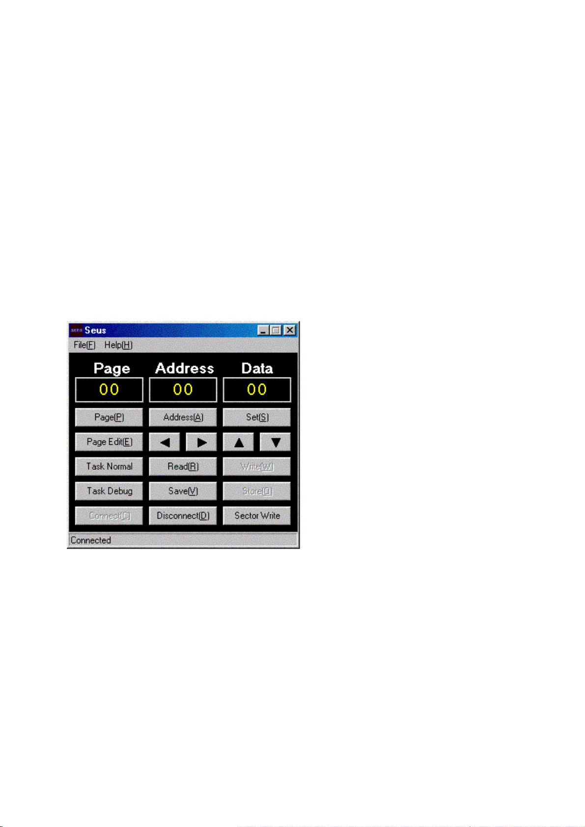
DSC-T1
1-1-4. Using Method of SEUS
The application for adjustment (SEUS) is used to change the coefficient for calculating the signal processing or EVR data. The SEUS
performs two-way communication between PC and set through
the USB terminal. The two-way communication result data can be
written to the nonvolatile memory.
1. Connection
1) Connect the HASP key to the USB terminal of the PC.
2) Connect the PC and set with the USB cable.
3) Confirm that the set starts in the USB mode.
4) Start the SEUS on the PC.
5) Click [Connect] on the SEUS screen. If the connection is normal, the SEUS screen will be as shown in Fig. 6-1-7, indicating the
“connected” state.
Note: The SEUS will go in
turned off (for instance, by resetting the set). In such a
case, click [Connect] on the SEUS screen to restore
the
“connected” state.
“disconnect" state, if the set is
2. Operation
• Page change
To change the page, click [Page] on the SEUS screen and enter
the page to be changed. The page is displayed in hexadecimal
notation.
• Address change
To change the address, click [Address] on the SEUS screen and
enter the address to be changed. The address is displayed in
hexadecimal notation.
• Data change
To change the data, click [Set] on the SEUS screen and enter
the data. The data is displayed in hexadecimal notation.
This operation does not write the data to the nonvolatile memory .
• Data saving
To write the all changed data to the nonvolatile memory, click
[Save] on the SEUS screen and wait for 3 sec.
• Data reading
The data displayed on the SEUS screen are the data values at
the time when the pages and addresses were set, and they are
not updated automatically. To check the data change, click
[Read] on the SEUS screen and update the displayed data.
1-1-5. Precaution on Use of SEUS
Wrong SEUS operation could clear correct adjustment data. To
prevent the data clear by mistake, it is recommended to save all
adjustment data by clicking [Page Edit] on the SEUS screen before starting the adjustment.
Fig. 6-1-7
Saving Method:
1) Click [Page Edit] on the SEUS screen to display the SEUS
PAGE EDIT screen.
2) Click [Page], and enter the page number to be saved.
3) Click [Page] to read the data to be saved from the camera.
4) Click [File] and save the data to PC.
Loading Method:
1) Select page: 00, address: 01 and set data: 01.
2) Click [Page Edit] on the SEUS screen to display the SEUS
PAGE EDIT screen.
3) Click [File] and load the data from PC.
4) Click [Write] on the SEUS PAGE EDIT screen.
5) Click [Close] to close the SEUS PAGE EDIT screen.
6) Click [Save] on the SEUS screen.
7) Wait for 3 sec.
8) Select page: 00, address: 01 and set data: 00.
6-7
Page 60

DSC-T1
1-2. AUTOMATIC ADJUSTMENT
The DSC-T1 is adjusted with the Automatic Adjustment Program.
The Automatic Adjustment Program controls automatically the adjustment operations that conventionally were entered manually on
the operation screen (however , partially some adjustments will require manual operation on the SEUS operation screen).
1-2-1. Precautions When Using Automatic Adjust-
ment Program
1) The Automatic Adjustment Program writes the adjustment results such as EVR data to the set through two-way communication with the camera via the SEUS. Accordingly, the Automatic Adjustment Program must be used in the environment
where the SEUS operates.
2) The program run time may vary depending on the environment of the personal computer used.
3) Even if the Automatic Adjustment Program is used without
starting the SEUS, the SEUS will start automatically when the
adjustment is executed. Howe ver, it may tak e time for the SEUS
to start, and therefore the Automatic Adjustment Program
should be used with the SEUS started in order to reduce the
program run time.
1-2-2. Start of Automatic Adjustment Program
Double-click the application file (DSC-T1 Auto-Adj
Ver_1.[]r
Note:[] (numeric value) of the file name var ies depending on the
[][]
.exe), and the Automatic Adjustment Program will start.
version of Automatic Adjustment Prog ram.
1-2-3. Function of Each Button on Main Menu Screen
When the Automatic Adjustment Program started, the Main Menu
screen in Fig. 6-1-8 will appear. On this screen, select each adjustment section.
1
2
3
4
Fig. 6-1-8
1 [VIDEO SYSTEM ADJUSTMENT] button
The “VIDEO SYSTEM ADJUSTMENT” screen appears.
2 [CAMERA SYSTEM ADJUSTMENT] button
The “CAMERA SYSTEM ADJUSTMENT” screen appears.
3 [LCD SYSTEM ADJUSTMENT] button
The “LCD SYSTEM ADJUSTMENT” screen appears.
4 [END] button
The Automatic Adjustment Program finishes.
6-8
Page 61
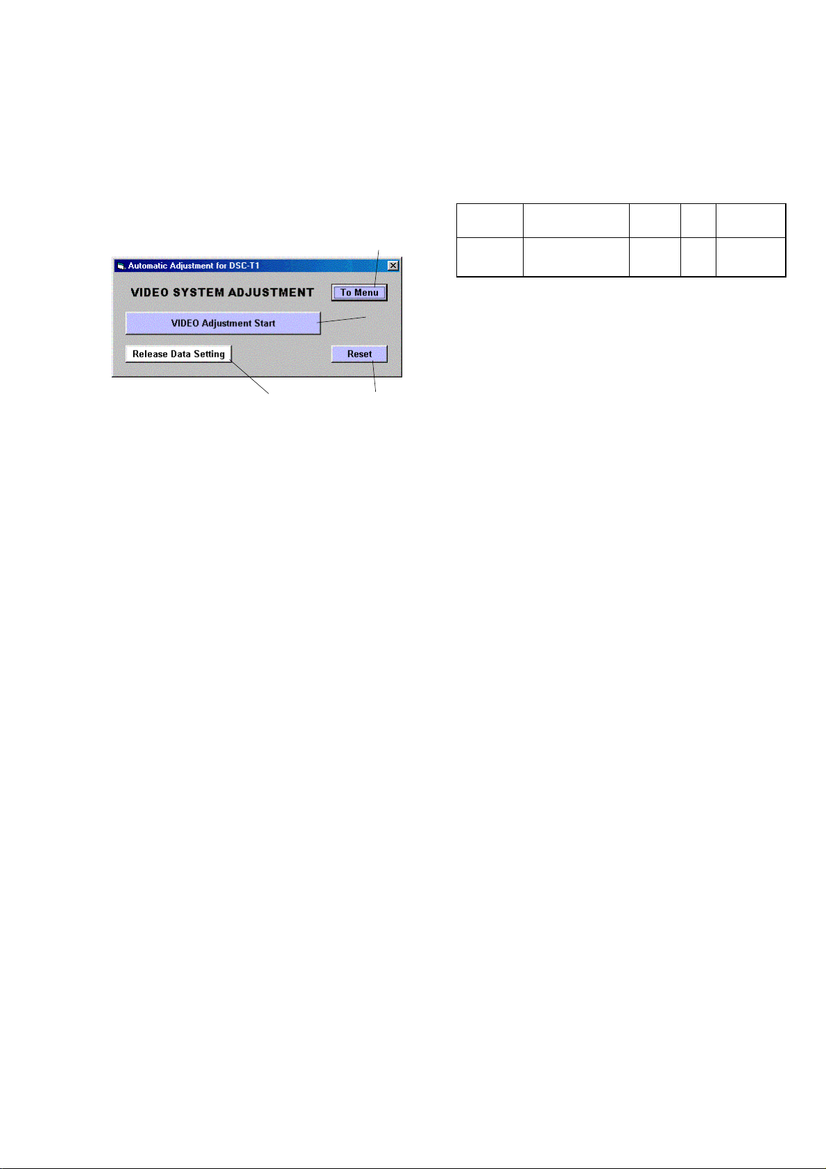
DSC-T1
1-3. VIDEO SYSTEM ADJUSTMENTS
1-3-1. Function of Each Button on Video System
Adjustment Screen
Click the
Menu screen, and the “VIDEO SYSTEM ADJUSTMENT” screen
in Fig. 6-1-9 will appear.
1 [To Menu] button
2 [VIDEO Adjustment Start] button
[VIDEO SYSTEM ADJUSTMENT] button on the Main
1
2
43
Fig. 6-1-9
The Main Menu screen comes back.
“Video Adjustment” starts.
1-3-2. Adjustment Items of VIDEO System
Adjustment
The adjustment items of video system adjustment are as listed in
Table 6-1-2. The Automatic Adjustment Program ex ecutes the adjustment items if the VIDEO Adjustment Start button is clicked.
Button
Name
VIDEO VIDEO Output
Adjustment Level Adj.
Adjustment Signal Page Address
Arbitrary 8F D0
Table 6-1-2
3 [Reset] button
This button functions same as the Reset button of the camera.
4 [Release Data Setting] button
The data setting at the adjustment is cancelled.
During the data setting, the button color changes from “white”
to “red”. When the data setting is cancelled, the button color
returns to “white”.
(Use this button when an error occurred in the video adjustment. If the adjustment completed successfully, the data setting is automatically cancelled and the button color returns to
“white”.)
6-9
Page 62

DSC-T1
1-3-3. Adjusting Method
[Automatic Adjustment Program execution items and
sequence]
1. Data Setting during Video Adj.
2. Video Output Level Adj.
3. Release of Data Setting during Video Adj.
[Specified value of video output level adj.]
Measurement Point Video terminal of AV OUT jack of
the cradle (75Ω terminated)
Measuring Instrument Oscilloscope
Specified Value Sync level:
A = 286 ± 5 mV (NTSC mode)
A = 300 ± 5 mV (PAL mode)
Burst level:
B = 286 ± 30 mV (NTSC mode)
B = 300 ± 30 mV (PAL mode)
[Adjusting method]
1) Click the [VIDEO Adjustment Start] button.
2) The Automatic Adjustment Program e xecutes the “1. Data Setting during Video Adj.”.
3) If “1. Data Setting during V ideo Adj.” completed successfully,
the next message is displayed during the execution of “2. V ideo
Output Level Adj.”. Using the UP/DOWN key on the SEUS
Operation screen, adjust so that the sync level of the video
signals satisfies the specified value. After the adjustment, check
that the burst level of the video signals satisfies the specified
value, and click the [OK] button in the message.
SEUS operation screen
UP/DOWN key
Fig. 6-1-12
Check on the osilloscope
B
A
Fig. 6-1-10
4) If the [OK] button button is clicked, “3. Release of Data Setting during Video Adj.” will be executed.
5) Upon successful completion of all items of the VIDEO adjustment, the following message is displayed. Click the [OK] but-
ton.
Fig. 6-1-11
H
Fig. 6-1-13
6-10
Page 63

1-4. CAMERA SYSTEM ADJUSTMENTS
1-4-1. Function of Each Button on Camera System
Adjustment Screen
Click the [CAMERA SYSTEM ADJUSTMENT] button on the Main
Menu screen, and the “CAMERA SYSTEM ADJUSTMENT”
screen in Fig. 6-1-14 will appear.
1
2
4
DSC-T1
Fig. 6-1-14
1 [To Menu] button
The Main Menu screen comes back.
2 Adjustment start buttons
• [CAMERA Adjustment 1 Start] button
“Camera Adjustment 1” starts.
• [CAMERA Adjustment 2 Start] button
“Camera Adjustment 2” starts.
• [CAMERA Adjustment 3 Start] button
“Camera Adjustment 3” starts.
• [CAMERA Adjustment 4 Start] button
“Camera Adjustment 4” starts.
3 [Reset] button
This button functions same as the Reset button of the camera.
4 [Release Data Setting] button
The data setting at the adjustment is cancelled.
During the data setting, the button color changes from “white”
to “red”. When the data setting is cancelled, the button color
returns to “white”.
(Use this button when an error occurred in the camera adjustment 1-4. If the adjustment completed successfully, the data
setting is automatically cancelled and the button color returns
to “white”.)
3
6-11
Page 64

DSC-T1
1-4-2. Adjustment Items of Camera System Adjust-
ment
The adjustment items of camera system adjustment are as listed in
Table 6-1-3. The Automatic Adjustment Program divides the adjustment items into four, camera adjustment 1-4. Clicking either
CAMERA Adjustment Start button allows the adjustment item
which corresponds to that button to be executed.
The adjustment conditions of the subject and filter vary depending on which item is adjusted. The Adjustment Program displays
an instruction for the subject and filter as a message during the
adjustment.
Button Name Adjustment Subject
(Note 1) Wide Limit Adj. Not required 6F 18, 19
CAMERA Adjustment 1 Flange Back Adj.
CAMERA Adjustment 2 Flange Back Check. (1.0m from front the lens)
F No. Compensation 6F 60 to 64, 6B to 6D
Mechanical Shutter Adj.
Light Value Adj. 6F 65 to 67
AWB 3200K Data Input 6E 04 to 21
AWB 5800K Data Input
CAMERA Adjustment 3
CAMERA Adjustment 4 Flash adjustment box 6F D8 to EF
Note 1: The Automatic Adjustment Program does not support
“Wide Limit Adjustment”.
Note 2: Dark Siemens star chart.
AWB 5800K Check
AWB 3200K Check
CCD Linearity Check
Color Reproduction Adj.
CCD White Defect
Compensation Check
CCD Black Defect
Compensation Check
Strobe Adj.
Auto Focus Illumination Check 6F 10 to 17
Siemens star chart with ND filter
for minipattern box (Note 2)
Siemens star chart with ND filter
(Luminance: 200 to 400 lux)
Clear chart (Standard picture frame)
Clear chart (Standard picture frame)
Filter C14 for color temperature
correction
Clear chart (Standard picture frame)
Color ber chart
(Standard picture frame)
Clear chart (Standard picture frame)
Adjustment Adjustment
Page Address
6F 18 to 53
6F 6B to 6D, B8 to D7
6E 00 to 03, 24 to 41
6E 60 to 67
6E 72 to 75
Table 6-1-3
6-12
Page 65

1-4-3. Adjusting Method
1. Wide Limit Adjustment
Adjustment to remove variations at the wide end of the inner focus lens.
Adjustment Page 6F
Adjustment Address 18, 19
DSC-T1
1-1.Adjusting method when the lens is replaced:
Adjusting method:
Order Page
1 00 01 01 Set the data.
2 6F 18 Set the data. (Note)
3 6F 19 Set the data. (Note)
4 7C 16 01 t 00 Change the data.
5 Save the data.
6 Wait for 2 sec.
7 Perform “Flange Back
Note: The data of page: 6F , address: 18 and 19, that are set in the
Orders 2 and 3 as described above, are shown on the data
sheet supplied with the replacement lens for repair.
Set the upper single byte of the 2-byte data shown on the
sheet to address: 18, and the lower byte of the data to the
address: 19.
Address
Data Procedure
(The data is OK if it is “00”.)
Adjustment”.
1-2.Adjusting method when replacement of lens
is not required and the SY-95 board is replaced:
When the data of page: 6F, address: 18 and 19 can be
read from the defective SY-95 board before replacement, and both of the data are not “00”:
Adjusting method:
Order Page
1 00 01 01 Set the data.
2 6F 18 Set the previous data
3 6F 19 Set the previous data
4 7C 16 01 t 00 Change the data.
5 Save the data.
6 Wait for 2 sec.
7 Perform “Flange Back
When the data of the page: 6F, address: 18 and 19 can
be read out from the defective SY-95 board before
replacing it, and both of the data are “00”:
1) Replace the lens with the replacement lens and perform “1-1.
Adjusting method when the lens is replaced”.
Address
Data Procedure
(The data is OK if it is “00”.)
Adjustment”.
Data for
Page: 6F,
Address: 18
Fig. 6-1-15
When the data of page: 6F, address: 18 and 19 cannot
be read from the defective SY-95 board:
1) Replace the lens with the replacement lens and perform “1-1.
Adjusting method when the lens is replaced”.
Note: The data of page: 7C, address: 16, that is set in the Order 4
of the adjusting method of 1-1 or 1-2, is “01” when shipped
from the factory. Let the data remain “00” after comple-
tion of the service adjustment.
Data for
Page: 6F,
Address: 19
6-13
Page 66

DSC-T1
2. CAMERA Adjustment 1
Note: When performing “CAMERA Adjustment 1”, connect the
cables after disassembling the cradle.
Unless the cradle is disassembled, the USB cable and the
power cable will interfere with the mini pattern box, and
thus the subject cannot be set correctly.
[Automatic Adjustment Program execution items and
sequence]
1. Data Setting during Camera Adj.
2. Flange Back Adj.
3. Release of Data Setting during Camera Adj.
[Adjusting method]
1) If the [CAMERA Adjustment 1 Start] button is clicked, the
following message is displayed.
If “Wide Limit Adjustment” is necessary, click the [Cancel]
button to interrupt the Adjustment Program, and perform “1.
Wide Limit Adjustment”.
Fig. 6-1-16
Preparation of Flange Back Adj.
1) The minipattern box is installed as shown in the following figure.
Note: The attachment lenses are not used.
2) Install the minipattern box so that the distance between it and
the front of lens of camera is less than 3 cm.
3) Make the height of minipattern box and the camera equal.
4) Check the output voltage of the regulated power supply is the
specified voltage ± 0.01 Vdc.
5) Check that the center of Siemens star chart meets the center of
shot image screen with the zoom lens at TELE end and WIDE
end respectively.
Specified voltage:The specified voltage varies according to the
minipattern box, so adjustment the power supply output voltage to the specified voltage written on the sheet which is supplied with the minipattern box.
Below 3 cm
Minipattern box
Camera
Regulated power supply
Output voltage : Specified voltage ± 0.01 Vdc
Output current : more than 3.5 A
2) If the [OK] button is clicked, the Automatic Adjustment Program executes “1. Data Setting during Camera Adj.”.
3) Upon successful completion of the “1. Data Setting during
Camera Adj.”, the follo wing message is displayed. Set the subject by referring to “Preparation of Flange Back Adj.”.
Fig. 6-1-17
4) If the [OK] button is clicked, “2. Flange Back Adj.” and “3.
Release of Data Setting during Camera Adj. ” will be ex ecuted.
5) Upon successful completion of all items of the CAMERA
Adjustment 1, the following message is displayed. Click the
[OK] button.
Red (+)
Black (–)
Yellow (SENS +)
White (SENS –)
Black (GND)
Need not connected
Fig. 6-1-19
Fig. 6-1-18
6-14
Page 67

DSC-T1
3. CAMERA Adjustment 2
[Automatic Adjustment Program execution items and
sequence]
1. Data Setting during Camera Adj.
2. Flange Back Check
3. Release of Data Setting during Camera Adj.
[Adjusting method]
1) Click the [CAMERA Adjustment 2 Start] button.
2) The Automatic Adjustment Pr ogram executes “1. Data Setting
during Camera Adj.”.
3) Upon successful completion of the “1. Data Setting during
Camera Adj. ”, the following message is displayed. Set the subject in accordance with the message.
Fig. 6-1-20
4) Click the [OK] button is clicked, “2. Flange Back Check” is
executed. The follo wing messages are displayed, and then operate the cameral to make a check in accordance with the messages.
6) Upon successful completion of all items of the CAMERA
Adjustment 2, the following message is displayed. Click the
[OK] button.
Fig. 6-1-22
Fig. 6-1-21
5) Upon completion of “2. Flange Back Check”, “3. Release of
Data Setting during Camera Adj.” is executed.
6-15
Page 68

DSC-T1
B
A
C
A = C =
B
2
E = F
V
EF
4. CAMERA Adjustment 3
[Automatic Adjustment Program execution items and
sequence]
1. Data Setting during Camera Adj.
2. Picture Frame Setting
3. F No. Compensation
4. Mechanical Shutter Adj.
5. Light Value Adj.
6. AWB 3200K Standard Data Input
7. AWB 5800K Standard Data Input
8. AWB 5800K Check
9. AWB 3200K Check
10. CCD Linearity Check
11. Color Reproduction Adj.
12. CCD White Defect Compensation Check
13. CCD Black Defect Compensation Check
14. Release of Data Setting during Camera Adj.
[Adjusting method]
1) Click the [CAMERA Adjustment 3 Start] button.
2) The Automatic Adjustment Program e xecutes the “1. Data Setting during Camera Adj.”.
3) Upon successful completion of “1. Data Setting during Camera Adj.”, “2. Picture Frame Setting” is executed. The follow-
ing message is displayed, and then referring to Fig. 6-1-25 to
Fig. 6-1-27, set the subject and click the [OK] button.
Check on the oscilloscope
Measurement Point:Video terminal of A/V OUT jack
(75Ω terminated)
1. Horizontal period
Fig. 6-1-23
After that, the next message is displayed. Then, change the chart
in accordance with the message.
Fig. 6-1-24
4) Click the [OK] button, and the items from “3. F No. Compensation” to “6. AWB 3200K Standard Data Input” will be executed.
Fig. 6-1-25
2. Vertical period
Fig. 6-1-26
Check on the monitor TV
A = C =
ABC
B
2
E
E = F
F
Color bar chart picture frame
Effective picture frame
Fig. 6-1-27
6-16
Page 69

DSC-T1
Burst position
5) Upon successful completion of the “AWB 3200K Check”, the
following message is displayed. Set the filter in accordance
with the message.
Fig. 6-1-28
6) Click the [OK] button, and the “7. AWB 5800K Standard Data
Input” and “8. AWB 5800K Check” will be executed.
7) Upon successful completion of the “AWB 5800K Check”, the
following message is displayed. Set the filter in accordance
with the message.
Fig. 6-1-29
8) Click the [OK] button, and the “9. AWB 3200K Check” and
“10. CCD Linearity Check” will be executed.
9) Upon successful completion of “10. CCD Linearity Check”,
the following message is displayed. Change the chart in accordance with the message.
11) Upon successful completion of “11. Color Reproduction Adj. ”,
the following message is displayed. Change the chart in accordance with the message.
Fig. 6-1-32
12) Click the [OK] button, and the “12. CCD White Defect Compensation Check”, “13. CCD Black Defect Compensation
Check” and “14. Release of Data Setting during Camera Adj.”
will be executed.
13) Upon successful completion of all items of the CAMERA
Adjustment 3, the following message is displayed. Click the
[OK] button.
Fig. 6-1-33
Fig. 6-1-30
10) Click the [OK] button, and “11. Color Reproduction Adj. ” will
be executed. The following messages are displayed in order,
and then operate the vectorscope to make a check with the
color reproduction frame in accordance with the message.
Fig. 6-1-31
Check on the vectorscope
Fig 6-1-34
6-17
Page 70

DSC-T1
5. CAMERA Adjustment 4
Note: “CAMERA Adjustment 4” is available only once after the
power is turned on. If the adjustment is retried, turn off the
power and turn on again.
[Automatic Adjustment Program execution items and
sequence]
1. Data Setting during Camera Adj.
2. Strobe Adj.
3. Auto Focus Illumination Check
4. Release of Data Setting during Camera Adj.
[Adjusting method]
1) Click the [CAMERA Adjustment 4 Start] button.
2) The Automatic Adjustment Program executes the “1. Data
Setting during Camera Adj.”.
3) Upon successful completion of the “1. Data Setting during
Camera Adj.”, the follo wing message is displayed. Set the subject in accordance with the message.
(For the Flash adjustment box, refer to “3. Preparing the Flash
Adjustment Box” (see page 6-6).)
6) Upon successful completion of “2. Strobe Adj.”, “3. Auto Fo-
cus Illumination Check” is executed. The following messages
are displayed, and then attach the AF illumination axis frame
to the monitor TV screen to make a check in accordance with
the messages.
Fig. 6-1-35
4) Press the [OK] button, and the “2. Strobe Adj.” will be ex-
ecuted.
5) During execution of “2. Strobe Adj.”, the following message
is displayed. After checking the flashing of strobe light, click
the [OK] button. (This message is displayed 2 times during
execution of adjustment.)
Fig. 6-1-36
Fig. 6-1-37
7) Upon successful completion of the “3. Auto Focus Illumination Check”, the “4. Release of Data Setting during Camera
Adj.” will be executed successively.
8) Upon successful completion of all items of the CAMERA
Adjustment 4, the following message is displayed. Click the
[OK] button.
Fig. 6-1-38
Check on the monitor TV
6-18
Fig. 6-1-39
Page 71

DSC-T1
1-5. LCD SYSTEM ADJUSTMENTS
1-5-1. Function of Each Button on LCD System
Adjustment Screen
Click the [LCD SYSTEM ADJUSTMENT] button on the Main
Menu screen, and the “LCD SYSTEM ADJUSTMENT” screen in
Fig. 6-1-40 will appear.
1
2
43
Fig. 6-1-40
1 [To Menu] button
The Main Menu screen comes back.
2 [LCD Adjustment Start] button
“LCD Adjustment” starts.
1-5-2. Adjustment Items of LCD System Adjustment
The adjustment items of LCD system adjustment are as listed in
Table 6-1-4. The Automatic Adjustment Program ex ecutes the adjustment items if the LCD Adjustment Start button is clicked.
Button
Name
LCD
Adjustment
Adjustment Signal Page Address
LCD Initial Data
Input 23 to 2C
VCO adj. 8F 23
Bright adj. 8F 25
Contrast adj. Arbitrary 8F 2C
V-COM adj. 8F 24
White Balance adj.
(1)
White Balance adj.
(2)
20, 21,
8F
8F 28, 2A
8F 29, 2B
Table 6-1-4
3 [Reset] button
This button functions same as the Reset button of the camera.
4 [Release Data Setting] button
The data setting at the adjustment is cancelled.
During the data setting, the button color changes from “white”
to “red”. When the data setting is cancelled, the button color
returns to “white”.
(Use this button when an error occurred in the LCD adjustment. If the adjustment completed successfully, the data setting is automatically cancelled and the button color returns to
“white”.)
6-19
Page 72

DSC-T1
1-5-3. Adjusting Method
[Automatic Adjustment Program execution items and
sequence]
1. LCD Initial Data Input
2. Data Setting during LCD Adj.
3. VCO Adj.
4. Bright Adj.
5. Contrast Adj.
6. V -COM Adj.
7. White Balance Adj. (1)
8. White Balance Adj. (2)
9. Release of Data Setting during LCD Adj.
[Adjusting method]
1) Click the [LCD Adjustment Start] button.
2) The Automatic Adjustment Program executes the items from
“1. LCD Initial Data Input” to “5. Contrast Adj.”.
3) Upon successful completion of the “5. Contrast Adj. ”, the following message is displayed during execution in “6. V-COM
Adj.”. On the SEUS screen, operate the UP/DOWN key so
that the brightness of portions A and B on the LCD panel is
equal. After the adjustment, click the [OK] button.
SEUS operation screen
UP/DOWN key
Fig. 6-1-44
Check on the LCD screen (V-COM Adj.)
A
B
Fig. 6-1-41
4) Upon completion of “6. V-COM Adj. ”, “7. White Balance Adj.
(1)” is executed. The following message is displayed, and then
check that LCD screen is not colored.
If colored, change the data of page: 8F, address: 28 and 2A on
the SEUS Operation screen to adjust so that the LCD screen is
not colored.
Fig. 6-1-42
5) If the [OK] button is clicked, “8. White Balance Adj. (2)” and
“9. Release of Data Setting during LCD Adj. ” will be ex ecuted.
A
B
B
A
A
B
Fig. 6-1-45
Fig. 6-1-43
6-20
Page 73

DSC-T1
This part indicates
the adjustment
item in which
an error occurred.
This part indicates
the adjustment
item in which
an error occurred.
1-6. ERROR
In case of an error during the execution of adjustment, the Automatic Adjustment Program interrupts the processing at that point,
and displays an error message, and then terminates the program
execution there.
1-6-1. Error Message
When an error message is displayed, perform the remedy given
below , and then retry adjustment. If the error message is displayed
though the remedy was performed, the circuits will be faulty.
1. Connect Error
Fig. 6-1-46
Symptom USB communication with the set is abnormal.
Cause • USB cable is not inserted tightly.
• Power supply is not installed correctly.
• Communication with SEUS is abnormal.
Remedy • Disconnect the USB cable once, and then re-
connect it tightly and check that the set is in
“USB Mode”.
• Install the power supply correctly.
• Start the SEUS and click the
check that the connection state is established.
2. RESET the CAMERA and Try Again
[Connect] to
3. Adjustment Time Out
Fig. 6-1-48
Symptom Adjustment does not finish within the specified
time.
Cause • Adjustment conditions are wrong.
• Data error exists in the camera.
Remedy • Check that the conditions such as a subject
are correct.
• Reset the camera.
4. Adjustment NG
Fig. 6-1-49
Symptom The adjusted data does not become the speci-
fied value.
Cause • Adjustment conditions are wrong.
• Data error exists in the camera.
Remedy • Check that the conditions such as a subject
are correct.
• Reset the camera.
Fig. 6-1-47
Symptom The camera is not ready for adjustment.
Cause • Data error exists in the camera.
Remedy • Reset the camera.
6-21
Page 74

DSC-T1
5. Data Save Error
How to cancel the
data setting during
adjustment is
display here.
Fig. 6-1-50
Symptom data cannot be saved normally. (The data set-
ting during adjustment cannot be cancelled)
Cause • Data writing to the flash memory failed.
• Connection is faulty.
• Power supply is not installed correctly.
Remedy • On the SEUS Operation screen,
to the pages and addresses displayed in the
message, and [Save] them. (Cancel manually the data setting during adjustment.)
• Check the connection.
• Install the power supply correctly.
[Set] the data
1-6-2. Precautions When an Error Occurred
The Automatic Adjustment Program sets the data for adjustment
before the adjustment starts. Accordingly, if the adjustment terminates by an error, the data during the adjustment may be left in the
camera.
Note 1: With this data left in the camera, the camera will not
operate normally.
In this case, the
“red” on the screen as shown in Fig. 6-1-51, 52 and 53. Click the
[Release Data Setting] button is displayed in
[Release Data Setting] button to cancel the data setting. When
the data setting is cancelled, the button color becomes “white”.
Note 2: When “Data Save Error” occurred, the [Release Data
Setting] button is displayed in “white”.
To cancel the data setting, perform it on the SEUS Operation screen. How to cancel the data setting is displayed
in the error message.
Video System Adjustment screen
Fig. 6-1-51
Camera System Adjustment screen
Fig. 6-1-52
LCD System Adjustment screen
6-22
Fig. 6-1-53
Page 75

DSC-T1
1-7. INITIALIZATION OF DATA
1-7-1. INITIALIZATION OF DATA
1. Initializing All Pages Data
By performing the following procedure, data of all the pages will
be initialized.
Initializing Method:
1) Select page: 00, address: 01, and set data: 01.
2) Click [Sector Write] on the SEUS screen to display the SEUS
SECTOR WRITE screen.
3) Check that the SET ID is “04”.
4) Click [All] of the ALL SELECT buttons to select all pages.
(Fig. 6-1-54. A)
5) Click [Write] to write the initializing data to the flash memory
of the camera.
6) Wait for 3 sec.
7) Click [Close] to close the SEUS PAGE EDIT screen.
Processing after Completing Initializing of data
Order Page
1 20 00 29 Set the data.
2 20 01 29 Set the data.
3 Check “Receive Paket Error” is
4 Turn on the power of the camera.
5 Click [Connect] on the SEUS
Address
Data Procedure
displayed on the SEUS screen.
screen.
2. Initializing Single Page Data
By performing the following procedure, data of the page that you
want to initialize will be initialized.
Initializing Method:
1) Select page: 00, address: 01, and set data: 01.
2) Click
3) Check that the SET ID is “04”.
4) Click “All” of the option buttons of the target page. (F ig. 6-1-54. B)
5) Click [Write] to write the initializing data to the flash memory
6) Wait for 3 sec.
7) Click [Close] to close the SEUS PAGE EDIT screen.
Processing after Completing Initializing of data
Order Page
[Sector Write] on the SEUS screen to display the SEUS
SECTOR WRITE screen.
of the camera.
Address
1 20 00 29 Set the data.
2 20 01 29 Set the data.
3 Check “Receive Paket Error” is
4 Turn on the po wer of the camera.
5 Click [Connect] on the SEUS
Data Procedure
displayed on the SEUS screen.
screen.
B
6-23
A
Fig. 6-1-54
Page 76

DSC-T1
6-2. SERVICE MODE
1. Setting the Test Mode
Page 2F Address 23
Data Function
80 Normal
01 Forced STILL mode power ON
02 Forced PLAY mode power ON
00 Forced MOVIE mode power ON
• Before setting the data, select page: 00, address: 01, and set data:
01.
• For page 2F, the data set is recorded in the non-v olatile memory
by saving data. In this case, take note that the test mode will not
be exited even when the main power is turned off.
• After completing adjustments/repairs, release the data setting .
1) Select page: 00, address: 01, and set data: 01.
2) Select page: 2F, address: 23, and set data: 80.
3) Save the data.
4) Wait for 3 sec.
5) Select page: 00, address: 01, and set data: 00.
2. Bit value discrimination
Bit values must be discriminated using the hexadecimal data for
following items. Use the table below to discriminate if the bit v alue
is “1” or “0”.
Hexadecimal data
bit3 to bit0 discrimination
bit7 to bit4 discrimination
Display on the
adjustment
remote
commander
0
1
2
3
4
5
6
7
A
B
8
9
A (A)
B (b)
C (c)
D (d)
E (E)
F (F)
bit3
or
bit7
0
0
0
0
0
0
0
0
1
1
1
1
1
1
1
1
Bit values
bit2
or
bit6
0
0
0
0
1
1
1
1
0
0
0
0
1
1
1
1
bit1
or
bit5
0
0
1
1
0
0
1
1
0
0
1
1
0
0
1
1
bit0
or
bit4
0
1
0
1
0
1
0
1
0
1
0
1
0
1
0
1
Examples: If the hexadecimal data is “8E”, the bit values for bit7 to bit4
are shown in the A column, and the bit values for bit3 to bit0
are shown in the B column.
6-24
Page 77

3. Switch check (1)
Page 20 Address 80
DSC-T1
Bit
POWER switch (XPWER ON)
0
(Control switch block S001)
Lens cover open switch (XLENS CAP ON)
2
(SY-95 board S401)
Function
When bit value=1
OFF
Closed
When bit value=0
ON
Open
Using method:
1) Select page: 20, address: 80.
2) Read the data. By discriminating the bit value of the data, the state of the switches can be discriminated.
4. Switch check (2)
Page 20 Address 90 to 92, 95
Using method:
1) Select page: 20, address: 90 to 92, 95.
2) Read the data. By discriminating the data, the pressed key can be discriminated.
Address
90
(MODE AD0)
(IC491
J6
)
91
(KEY AD1)
(IC491
H6
)
92
(KEY AD2)
(IC491
G6
)
94
(MODE DIAL0)
(IC491
J8
)
00 to 0B
MENU
(Control switch block)
(S007)
Control button UP
(Control switch block)
(S006)
WIDE
(Control switch block)
(S003)
Mode switch MOVIE
(MS-148 board)
(S101)
0C to 26
Control button LEFT
(Control switch block)
(S005)
IMAGE SIZE/DELETE
(Control switch block)
(S009)
TELE
(Control switch block)
(S004)
Mode switch STILL
(MS-148 board)
(S101)
Data
27 to 47
DISPLAY/LCD BACK LIGHT
(Control switch block)
(S013)
Control button RIGHT
(Control switch block)
(S010)
Mode switch PLAY
(MS-148 board)
(S101)
48 to 72
Control button DOWN
(Control switch block)
(S011)
Control button SET
(Control switch block)
(S008)
73 to FF
No key input
No key input
No key input
5. Switch check (3)
Page 80 Address 13
Function
Shutter button (XAE LOCK SW)
When data = 00
Off
When data = 01
On
When data = 02
On
(Control switch block S002)
Shutter button (XSHTR ON SW)
Off
Off
On
(Control switch block S002)
Using method:
1) Select page: 80, address: 13.
2) Read the data. By discriminating the data, the state of the switches can be discriminated.
6-25
Page 78

DSC-T1
6. LED check
Page 20 Address 04
Page 80 Address 12
Page 8E Address FE
Using method:
1) Select page: 00, address: 01, set data: 01.
2) Select page: 8E, address: FE, set data: 20.
3) Select page: 80, address: 12, set data: 01.
4) Select page: 20, address: 04, set data: 02.
5) Check that all LED (Power, Flash/Charge, MS access, AF illmination) are lit.
6) Select page: 20, address: 04, set data: 00.
7) Select page: 80, address: 12, set data: 00.
8) Select page: 8E, address: FE, set data: 00.
9) Select page: 00, address: 01, set data: 00.
7. Record of Use check
Page 4F Address 94 to 97
Address
94
95
96
97
Using method:
1) The recording counter data is displayed at page: 4F, addresses: 94 to 97. These data are named D94, D95, D96 and D97 respectively.
2) Calculate the recording counter (N) using following equation. (Hexadecimal calculation)
N = D97 + D96 × 100 + D95 × 10000 + D94 × 1000000
8. Self Diagnostics Log check
Page 20 Address B0 to B8
Address
B0
B1
B2
B3
B4
B5
B6
B7
B8
Function
Recording counter
(Hexadecimal)
Initial value
00
00
00
00
00
00
00
00
00
“Repaired by” code (Occurred 1st time) *1
“Block function” code (Occurred 1st time)
“Detailed” code (Occurred 1st time)
“Repaired by” code (Occurred 2nd time) *1
“Block function” code (Occurred 2nd time)
“Detailed” code (Occurred 2nd time)
“Repaired by” code (Occurred 3rd time) *1
“Block function” code (Occurred 3rd time)
“Detailed” code (Occurred 3rd time)
Remarks
1000000-digit and 1000000-digit
1000000-digit and 10000-digit
1000-digit and 100-digit
10-digit and 1-digit
Function
*1: “C” t “01”, “E” t “03”
Using method:
1) The self diagnostics log is displayed at page: 20, addresses: B0 to B5.
Note: These data will be erased when the lithium battery (CN-198 board) is removed.
6-26
Page 79

〈FOR CAMERA COLOR REPRODUCTION ADJUSTMENT〉
DSC-T1
Take a copy of CAMERA COLOR
REPRODUCTION FRAME with a
clear sheet for use.
✂
〈AF ILLUMINATION FRAME〉
✂
6-27E
6-27
Page 80

[Description of main button functions on toolbar of the Adobe Acrobat Reader Ver5.0 (for Windows)]
Toolbar
Printing a text
1. Click the Print button .
2. Specify a printer, print range, number of copies, and other options, and then click [OK].
Application of printing:
To set a range to be printed within a page, select the graphic
selection tool
be printed, and then click the Print button.
and drag on the page to enclose a range to
Finding a text
1. Click the Find button .
2. Enter a character string to be found into a text box, and click
the [Find]. (Specify the find options as necessary)
Application to the Service Manual:
To execute “find” from current page toward the previous pages,
select the check box “Find Backward” and then click the
“Find”.
3. Open the find dialog box again, and click the [Find Again] and
you can find the matched character strings displayed next.
(Character strings entered previously are displayed as they are
in the text box.)
Reversing the screens displayed once
•To reverse the previous screens (operation) one by one, click
.
the
•To advance the reversed screens (operation) one by one, click
.
the
Application to the Service Manual:
This function allows you to go and back between circuit diagram and printed circuit board diagram, and accordingly it
will be convenient for the voltage check.
Moving with link
1. Select either palm tool , zoom tool , text selection tool
, or graphic selection tool .
2. Place the pointer in the position in a text where the link exists
(such as a button on cover and the table of contents page, or
blue characters on the removal flowchart page or drawing
page), and the pointer will change to the forefinger form .
3. Then, click the link. (You will go to the link destination.)
Moving with bookmark:
Click an item (text) on the bookmark pallet, and you can move
to the link destination. Also, clicking can display the
hidden items.
(To go back to original state, click )
Application to the Service Manual:
The parts on the drawing pages (block diagrams, circuit diagrams, printed circuit boards) and parts list pages in a text
can be found using this find function. For example, find a
Ref. No. of IC on the block diagram, and click the [Find Again]
continuously, so that you can move to the Ref. No. of IC on
the circuit diagram or printed circuit board diagram successively.
Note: The find function may not be applied to the Service
Manual depending on the date of issue.
Switching a page
•To move to the first page, click the .
•To move to the last page, click the
•To move to the previous page, click the
•To move to the next page, click the
.
.
.
Zooming or rotating the screen display
“Zoom in/out”
• Click the triangle button in the zoom control box to select the
display magnification. Or, you may click
ing in or out.
“Rotate”
• Click rotate tool , and the page then rotates 90 degrees each.
or for zoom-
Application to the Service Manual:
The printed circuit board diagram you see now can be changed
to the same direction as the set.
 Loading...