

Sony DSCP-92 Service manual

DSC-P92
SERVICE MANUAL
Ver 1.0 2003. 04
Revision History
Revision History
Link
Link
SPECIFICATIONS
BLOCK DIAGRAMS
BLOCK DIAGRAMS
LEVEL 2
US Model
Canadian Model
AEP Model
UK Model
E Model
Australian Model
Hong Kong Model
Korea Model
Chinese Model
Tourist Model
Brazilian Model
Japanese Model
PRINTED WIRING BOARDS
PRINTED WIRING BOARDSSPECIFICATIONS
SERVICE NOTE
SERVICE NOTE
DISASSEMBLY
DISASSEMBLY
• For INSTRUCTION MANUAL, refer to SERVICE MANUAL, LEVEL 1 (987624941.pdf).
• Reference No. search on printed wiring boards is available.
On the SY-93 board
This service manual provides the information that is premised the circuit board replacement service and not intended repair
inside the SY-93 board.
Therefore, schematic diagram, printed wiring board, waveforms, mounted parts location and electrical parts list of the SY-93
board are not shown.
The following pages are not shown.
Schematic diagram .............................Pages 4-7 to 4-26
Printed wiring board ............................Pages 4-39 to 4-42
Waveforms ...........................................
FRAME SCHEMATIC DIAGRAMS
FRAME SCHEMATIC DIAGRAMS
SCHEMATIC DIAGRAMS
SCHEMATIC DIAGRAMS
Mounted parts location .............................
Electrical parts list ................................... Pages 5-6 to 5-11
Pages 4-45 to 4-46
REPAIR PARTS LIST
REPAIR PARTS LIST
Page 4-48
DIGITAL STILL CAMERA

DSC-P92
COVER
COVER
x Camera
[System]
Image device 9.04 mm (1/1.8 type) color
Total pixels number of camera
Effective pixels number of camer a
Lens 3× zoom lens
Exposure control
White balance
File format (DCF compliant)
Recording media
Flash Recommended distance
[Output connectors]
A/V OUT (MONO) jack (Monaural)
USB jack mini-B
CCD
Primary color filter
Approx. 5 255 000 pixels
Approx. 5 090 000 pixels
f=8.0 to 24.0 mm
(35 mm camera conversion: 39 to
117mm (1
F2.8-5.6
Automatic, Program, Twilight,
Twilight portrait, Landscape, Snow,
Beach
Automatic, Daylight, Cloudy,
Fluorescent, Incandescent
Still images: Exif Ver. 2.2, JPEG
compliant, GIF (for Clip Motion),
DPOF compatible
Audio with still image: MPEG1
compliant (Monaural)
Movies: MPEG1 compliant
(Monaural)
“Memory Stick”
0.5 to 3.8 m (19
12 feet 5
0.6 to 2.5 m (23
8 feet 2
(when ISO sensitivity is set to Auto)
Minijack
Video: 1 Vp-p, 75 Ω, unbalanced,
sync negative
Audio: 327 mV (at a 47 kΩ load)
Output impedance 2.2 kΩ
9
/16 to 4 5/8 inches))
3
/4 inches to
19
/32 inches) (W)/
5
/8 inches to
7
/16 inches) (T)
SPECIFICATIONS
[LCD screen]
LCD panel used
Total number of dots
[Power, general]
Power AA nickel hydride batteries (2)
Power consumption (when recording)
Operating temperature range
Storage temperature range
Dimensions 119.5 × 57.7 × 36.8 mm
Mass Approx. 260.5 g (9.2 oz) (two
Microphone Electret condenser microphone
Speaker Dynamic speaker
Exif Print Compatible
PRINT Image Matching II
x BC-CS2A/CS2B Ni-MH battery
charger
Power requirements
Output voltage
Operating temperature range
Storage temperature range
Dimensions 71 × 30 × 91 mm
Mass Approx. 90 g (3 oz)
3.8 cm (1.5 type) TFT drive
123 200 (560×220) dots
2.4 V
AC-LS5 AC Adaptor
(not supplied), 4.2 V
1.9 W
0° to +40°C (32° to +104°F)
−20° to +60°C (−4° to +140°F)
3
(4
/4 × 2 3/8 × 1 1/2 inches)
(W/H/D, protruding portions not
included)
batteries, “Memory Stick” and wrist
strap included)
Compatible
AC 100 to 240V 50/60Hz
3 W
AA : DC 1.4 V 400 mA
AAA : DC 1.4 V 160 mA
0° to +40°C (32° to +104°F)
−20° to +60°C (−4° to +140°F)
7
/8 × 1 3/16 × 3 5/8 inches) (W/H/
(2
D)
× 2
× 2
x AC-LS5 AC Adaptor (not supplied)
Power requirements
Rated output voltage
Operating temperature range
Storage temperature range
Maximum dimensions
Mass Approx. 130 g (5 oz)
AC 100 to 240 V, 50/60 Hz
11 W 0.16 to 0.09 A
DC 4.2 V, 1.5 A
0° to +40°C (32° to +104°F)
−20° to +60°C (−4° to +140°F)
Approx. 48
1
× 29 × 81 mm (1
3
/16 × 3 1/4 inches) (W/H/D)
15
/16 ×
Accessories
HR6 (size AA) Ni-MH batteries (2)
Battery case
BC-CS2A/CS2B Ni-MH Battery charger (1)
Power cord (mains lead) (1)
USB cable (1)
A/V connecting cable (1)
Wrist strap (1)
“Memory St ick” (16MB ) (1)
CD-ROM (USB driver: SPVD-010) (1)
Operating Instructions (1)
Design and specifications are subject to change
without notice.
CAUTION :
Danger of explosion if battery is incorrectly replaced.
Replace only with the same or equivalent type.
SAFETY-RELATED COMPONENT WARNING!!
COMPONENTS IDENTIFIED BY MARK 0 OR DOTTED LINE WITH
MARK 0 ON THE SCHEMATIC DIAGRAMS AND IN THE PARTS
LIST ARE CRITICAL TO SAFE OPERATION. REPLACE THESE
COMPONENTS WITH SONY PARTS WHOSE PART NUMBERS
APPEAR AS SHOWN IN THIS MANUAL OR IN SUPPLEMENTS
PUBLISHED BY SONY.
ATTENTION AU COMPOSANT AYANT RAPPORT
À LA SÉCURITÉ!
LES COMPOSANTS IDENTIFÉS PAR UNE MARQUE 0 SUR LES
DIAGRAMMES SCHÉMATIQUES ET LA LISTE DES PIÈCES SONT
CRITIQUES POUR LA SÉCURITÉ DE FONCTIONNEMENT. NE
REMPLACER CES COMPOSANTS QUE PAR DES PIÈSES SONY
DONT LES NUMÉROS SONT DONNÉS DANS CE MANUEL OU
DANS LES SUPPÉMENTS PUBLIÉS PAR SONY.
— 2 —

SAFETY CHECK-OUT
After correcting the original service problem, perform the following
safety checks before releasing the set to the customer.
DSC-P92
1. Check the area of your repair for unsoldered or poorly-soldered
connections. Check the entire board surface for solder splashes
and bridges.
2. Check the interboard wiring to ensure that no wires are
"pinched" or contact high-wattage resistors.
3. Look for unauthorized replacement parts, particularly
transistors, that were installed during a previous repair. Point
them out to the customer and recommend their replacement.
4. Look for parts which, through functioning, show obvious signs
of deterioration. Point them out to the customer and
recommend their replacement.
5. Check the B+ voltage to see it is at the values specified.
6. Flexible Circuit Board Repairing
• Keep the temperature of the soldering iron around 270˚C
during repairing.
• Do not touch the soldering iron on the same conductor of the
circuit board (within 3 times).
• Be careful not to apply force on the conductor when soldering
or unsoldering.
Unleaded solder
Boards requiring use of unleaded solder are printed with the leadfree mark (LF) indicating the solder contains no lead.
(Caution: Some printed circuit boards may not come printed with
the lead free mark due to their particular size.)
: LEAD FREE MARK
Unleaded solder has the following characteristics.
• Unleaded solder melts at a temperature about 40°C higher than
ordinary solder.
Ordinary soldering irons can be used but the iron tip has to be
applied to the solder joint for a slightly longer time.
Soldering irons using a temperature regulator should be set to
about 350°C.
Caution: The printed pattern (copper foil) may peel away if the
heated tip is applied for too long, so be careful!
• Strong viscosity
Unleaded solder is more viscous (sticky, less prone to flow) than
ordinary solder so use caution not to let solder bridges occur such
as on IC pins, etc.
• Usable with ordinary solder
It is best to use only unleaded solder but unleaded solder may
also be added to ordinary solder.
— 3 —
DSC-P92
TABLE OF CONTENTS
1. SERVICE NOTE ........................................................1-1
2. DISASSEMBLY
2-1. CABINET (REAR) BLOCK ASSEMBLY ·····················2-2
2-2. BLOCK LIGHT GUIDE PLATE, LCD MODULE
(ACX309AKB-2), CONTROL SWITCH BLOCK
(SW-391), LITHIUM BATTERY ····································2-3
2-3. MAIN BLOCK ASSEMBLY ··········································2-4
2-4. UNIT PARTS (UA-002) ··················································2-4
2-5. ZOOM LENS (CE01B), CCD BLOCK ASSEMBLY ····2-5
2-6. MEMORY STICK CONNECTOR,
JK BLOCK (JK-252)·······················································2-6
2-7. CONTROL SWITCH BLOCK (RL-059),
ST-82 BOARD ································································2-6
2-8. SY-93 BOARD ································································2-7
2-9. FLASH UNIT··································································2-9
2-10. CIRCUIT BOARDS LOCATION ·································2-10
2-11. FLEXIBLE BOARDS LOCATION ······························2-11
3. BLOCK DIAGRAMS
3-1. OVERALL BLOCK DIAGRAM (1/2) ···························3-1
3-2. OVERALL BLOCK DIAGRAM (2/2) ···························3-3
3-3. POWER BLOCK DIAGRAM (1/2) ································3-5
3-4. POWER BLOCK DIAGRAM (2/2) ································3-7
5. REPAIR PARTS LIST
5-1. EXPLODED VIEWS ······················································ 5-1
5-1-1.CABINET (FRONT) SECTION ·····································5-3
5-1-2.MAIN BLOCK SECTION ·············································· 5-4
5-1-3.CABINET (REAR) BLOCK SECTION ·························5-5
5-2. ELECTRICAL PARTS LIST ········································5-12
Parts list of the SY-93 board are not shown.
Pages from 5-6 to 5-11 are not shown.
4. PRINTED WIRING BOARDS AND
SCHEMATIC DIAGRAMS
4-1. FRAME SCHEMATIC DIAGRAM (1/2) ·······················4-1
FRAME SCHEMATIC DIAGRAM (2/2) ·······················4-3
4-2. SCHEMATIC DIAGRAMS
Shematic diagram of the SY-93 board are not shown.
Pages from 4-7 to 4-25 are not shown.
• ST-82 (FLASH DRIVE)/FP-643 FLEXIBLE
SCHEMATIC DIAGRAM ····························4-27
• JK BLOCK (JK-252) (JACK)
SCHEMATIC DIAGRAM ····························4-29
• CONTROL SWITCH BLOCK (SW-391)
(LCD CONTROL)
SCHEMATIC DIAGRAM ····························4-31
• RL-059 (POWER/SHUTTER SWITCH)
SCHEMATIC DIAGRAM ····························4-33
• UA-002 (MIC, AF LED)
SCHEMATIC DIAGRAM ····························4-33
4-3. PRINTED WIRING BOARDS
• ST-82 (FLASH DRIVE)
PRINTED WIRING BOARD ·······················4-37
Printed wiring board of the SY-93 board are not shown.
Pages from 4-39 to 4-42 are not shown.
• JK BLOCK (JK-252) (JACK)
FLEXIBLE BOARD·····································4-43
4-4. WAVEFORMS ······························································4-45
Waveforms of the SY-93 board are not shown.
Pages 4-45 to 4-46 are not shown.
4-5. MOUNTED PARTS LOCATION ·································4-47
Mounted parts location of the SY-93 board is not shown.
Page 4-48 is not shown.
— 4 —

DSC-P92
COVER
COVER
SECTION 1
SERVICE NOTE
• NOTE FOR REPAIR
Make sure that the flat cable and flexible board are not cracked of
bent at the terminal.
Do not insert the cable insufficiently nor crookedly.
Cut and remove the part of gilt
which comes off at the point.
(Take care that there are
some pieces of gilt left inside)
When remove a connector, don't pull at wire of connector.
Be in danger of the snapping of a wire.
When installing a connector, don't press down at wire of connector.
Be in danger of the snapping of a wire.
[Discharging of the FLASH unit’s charging capacitor]
The charging capacitor of the FLASH unit is charged up to the
maximum 300 V potential.
There is a danger of electric shock by this high voltage when the
capacitor is handled by hand. The electric shock is caused by the
charged voltage which is kept without discharging when the main
power of the DSC-P92 is simply turned off. Therefore, the remaining
voltage must be discharged as described below.
Preparing the Short Jig
To preparing the short jig. a small clip is attached to each end of a
resistor of 1 kΩ /1 W (1-215-869-11)
Wrap insulating tape fully around the leads of the resistor to prevent
electrical shock.
Discharging the Capacitor
Short circuits between the positive and the negative terminals of
charged capacitor with the short jig about 10 seconds.
Capacitor
1 kΩ/1 W
Wrap insulating tape.
Shorting jig
(1k
Ω
/ 1w)
ST-82 BOARD
1-1
DSC-P92
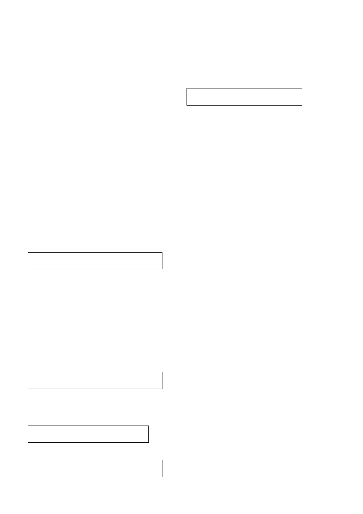
[Description on Self-diagnosis Display]
Self-diagnosis display
• C: ss: ss
• E: ss: ss
The contents which can be handled
by customer, are displayed.
The contents which can be handled
by engineer, are displayed.
Display Code
C:32:01
C:13:01
E:91:01
E:61:00 *1
E61:10 *1
Note : The error code is cleared if the battery is removed, except defective flash unit.
*1: The error display is given in two ways.
Turn off the main power then back on.
Replace the memory stick.
Format the memory stick with the DSC-P92.
Checking of flash unit or replacement of
flash unit.
Checking of lens drive circuit
Countermeasure
Trouble with hardware.
• The type of memory stick that cannot be
used by this machine, is inserted.
• Data is damaged.
• Unformatted memory stick is inserted.
Abnormality when flash is being
charged.
When failed in the focus initialization.
Cause
Caution Display During Error
SYSTEM ERROR
MS ERROR
Flash LED
Flash display
Flashing at 3.2 Hz
—
1-2E

DSC-P92
COVER
COVER
SECTION 2
DISASSEMBLY
The following flow chart shows the disassembly procedure.
DISASSEMBLY
DISASSEMBLY
HELP
SY-93 board
service position
HELP
HELP
DISASSEMBLY
HELP
Discharging the Capacitor
DISASSEMBLY
DISASSEMBLY
DISASSEMBLY
DISASSEMBLY
DISASSEMBLY
HELP
PROCEDURE OF REMOVING THE SY-93 BOARD (SERVICE POSITION)
1 2-1. CABINET (REAR) BLOCK ASSEMBLY ...................................................
2 2-2. BLOCK LIGHT GUIDE PLATE, LCD MODULE (ACX309AKB-2), ...........
CONTROL SWITCH BLOCK (SW-391), LITHIUM BATTERY
3 2-3. MAIN BLOCK ASSEMBLY .......................................................................
4 2-4. UNIT PARTS (UA-002) ............................................................................
5 2-5. ZOOM LENS (CE01B), CCD BLOCK ASSEMBLY ..................................
6 2-6. MEMORY STICK CONNECTOR, JK BLOCK (JK-252) ...........................
7 2-7. CONTROL SWITCH BLOCK (RL-059), ST-82 BOARD ...........................
8 2-8. SY-93 BOARD .........................................................................................
(page 2-2)
(page 2-3)
(page 2-4)
(page 2-4)
(page 2-5)
(page 2-6)
(page 2-6)
(page 2-7)
2-1
DSC-P92
NOTE: Follow the disassembly procedure in the numerical order given.
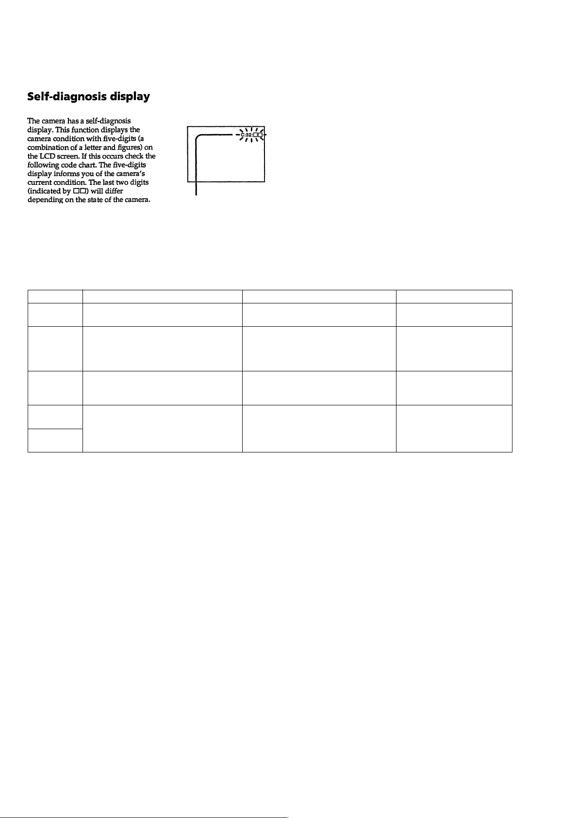
2-1. CABINET (REAR) BLOCK ASSEMBLY
Attach the Tape (Y) as shown in the illustration.
6
Claw
Caution
8
Claw
4
Open the
MS lid.
7
Claw
5
lock ace, p2
3
Screw (M2 × 4),
lock ace, p2
Screw (M2 × 4),
2
Screw (M2 × 4),
lock ace, p2
qa
Tape (Y)
Tape (Y)SY-93 board
qs
Control switch block (SW-391)(39P)
q;
Claw
9
Claw
qd
Cabinet (rear) block assembly
1
Screw (M2 × 4),
lock ace, p2
2-2
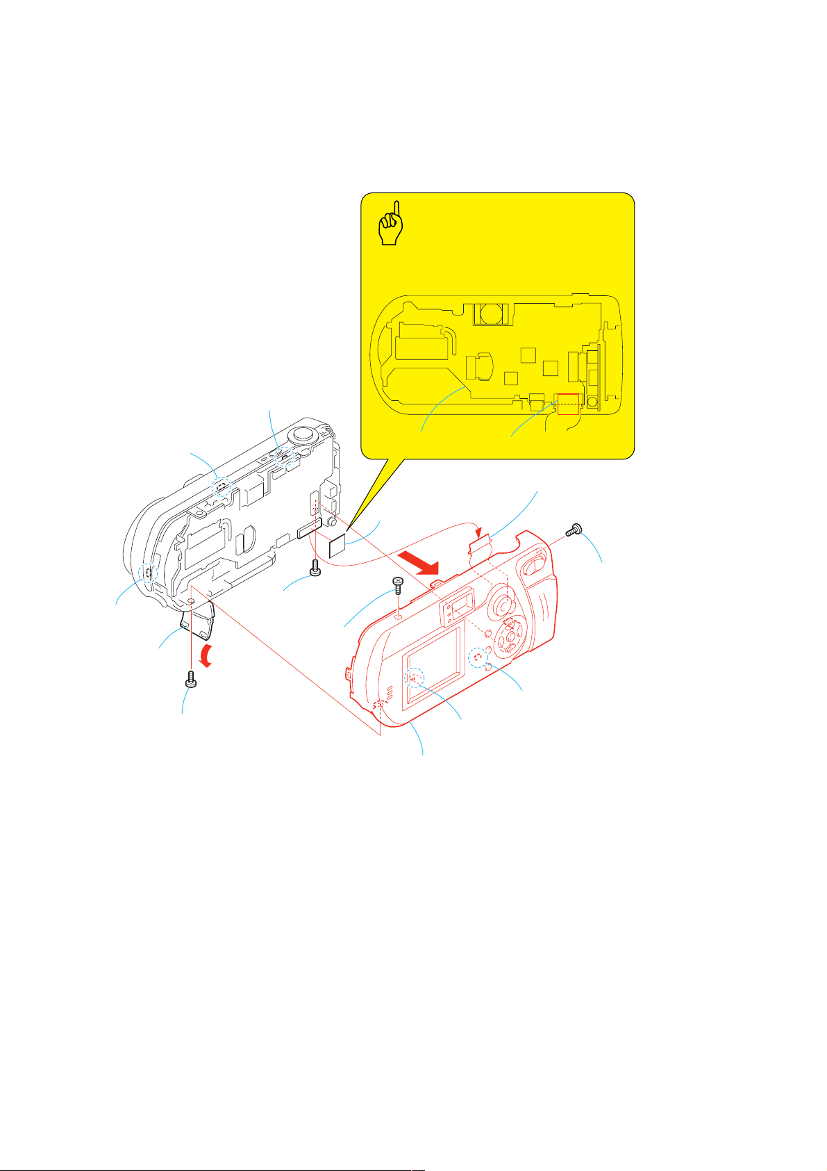
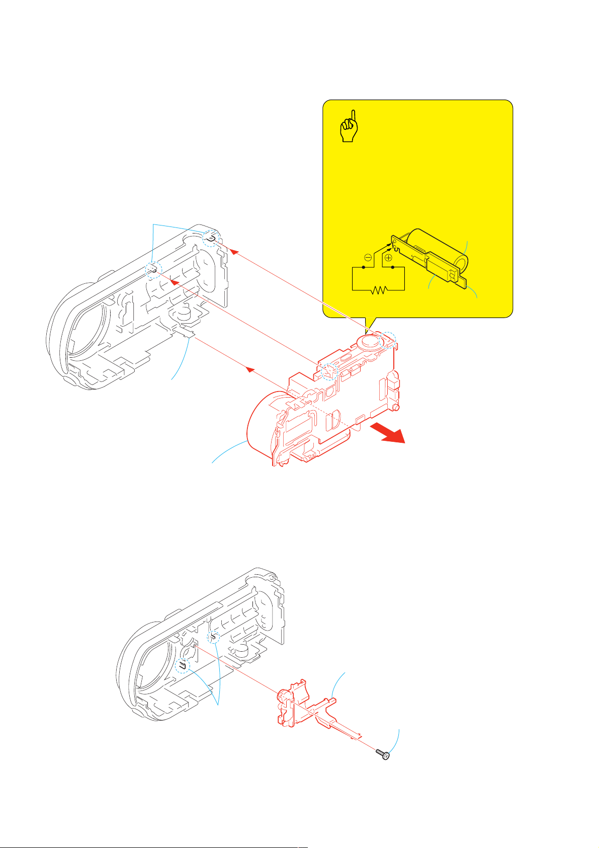
2-2. BLOCK LIGHT GUIDE PLATE, LCD MODULE (ACX309AKB-2),
Danger of explosion if batteryis incorrectly replaced.
Replace only with the same or equivalent type.
5
Control switch block (SW-391)
Control switch block (SW-391)
When installing it,
align the switch position
as shown.
1
Four tapping screws
(M1.7
×
4)
2
Two tapping screws
(M1.7
×
4)
4
LCD module
(ACX309AKB-2) (24P)
3
Block light guide plate
(6P)
Caution
6
Remove soldering
from the two points.
7
Lithium battery
Lithium battery
Caution
CONTROL SWITCH BLOCK (SW-391), LITHIUM BATTERY
DSC-P92
2-3
DSC-P92
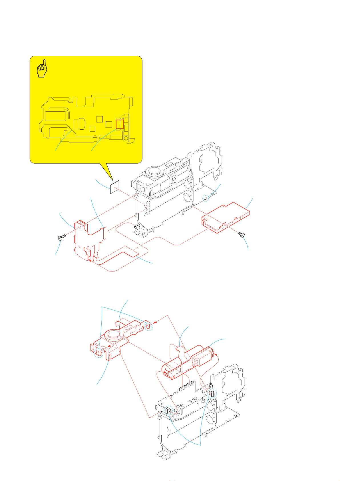
2-3. MAIN BLOCK ASSEMBLY
2
Two claws
Caution
The power supply capacitor of the Flash unit is
charged to the voltage as high as 300 V at a
maximum. The high voltage is not discharged
even after the main power of the machine is
simply turned off and the charged potential still
remains.
Discharge the residual voltage by referring to
Service Note (page 1-1).
Capacitor
1
Unit parts (UA-002)
(10P)
3
2-4. UNIT PARTS (UA-002)
Main block assembly
Shorting jig
Ω
/ 1w)
(1k
Flash unit
ST-82 board
2
Two cl
aws
2-4
3
Unit parts (UA-002)
1
Tapping screws, p2
(1.7 × 5)

2-5. ZOOM LENS (CE01B), CCD BLOCK ASSEMBLY
2
Zoom lens (CE01B) (27P)
7
Optical filter block
6
Light interception plate
q;
CCD block assembly
DSC-P92
Caution
Attach the Tape (Y) as shown in the illustration.
Tape (Y)
8
Seal rubber (K)
9
Remove the solderings.
5
Three screws
(1.7
×
4)
1
Tape (Y)
4
Plate cooling CCD
3
Two tapping screw, p2
×
(1.7
5)
2-5
DSC-P92
r
d
2-6. MEMORY STICK CONNECTOR, JK BLOCK (JK-252)
Caution
Attach the Tape (Y) as shown in the illustration.
Tape (Y)SY-93 board
6
Tape (Y)
2
Claw
7
JK BLOCK (JK-252) (39P)
8
JK BLOCK (JK-252)
5
Tapping screw, p2
(1.7
×
5)
3
JK BLOCK (JK-252) (10P)
2-7. CONTROL SWITCH BLOCK (RL-059), ST-82 BOARD
2
Control switch block (RL-059)(10P)
1
Two claws
5
FP-643 flexible board
(12P)
4
Memory stick connecto
1
Tapping screw
(1.7
×
4)
6
ST-82 boar
3
Control switch block (RL-059)
2-6
4
Two claws
2-8. SY-93 BOARD
)
DSC-P92
Caution
When removing the harness,
be sure to pull the harness up at the
right angle with the board while pressing
down the connector on the circuit board.
Connector
2
Battery holder
(with terminal)
(4P)
3
SY-93 board
1
Four screws(M2 × 3
2-7

DSC-P92
[SERVICE POSITION (SY-93 BOARD)]
Cabinet (rear) block assembly
(39P)
Memory stick connector
(10P)
JK BLOCK
(JK-252)
AC power
adaptor
AC IN
CN706
CN201
(10P)
Unit parts(UA-002)
Zoom lens (CE01B)
“ Never remove the lens unless removal
is required at the event of checking the
CCD imager and others.’’
(27P)
SY-93 board
PROCEDURE OF REMOVING THE SY-93 BOARD (SERVICE POSITION)
1 2-1. CABINET (REAR) BLOCK ASSEMBLY ...................................................
2 2-2. BLOCK LIGHT GUIDE PLATE, LCD MODULE (ACX309AKB-2), ...........
CONTROL SWITCH BLOCK (SW-391), LITHIUM BATTERY
3 2-3. MAIN BLOCK ASSEMBLY .......................................................................
4 2-4. UNIT PARTS (UA-002) ............................................................................
5 2-5. ZOOM LENS (CE01B), CCD BLOCK ASSEMBLY ..................................
6 2-6. MEMORY STICK CONNECTOR, JK BLOCK (JK-252) ...........................
7 2-7. CONTROL SWITCH BLOCK (RL-059), ST-82 BOARD ...........................
8 2-8. SY-93 BOARD .........................................................................................
CN702
CN705
(10P)
Control switch block (RL-059)
(39P)
CN701
CN704
(12P)
(page 2-2)
(page 2-3)
(page 2-4)
(page 2-4)
(page 2-5)
(page 2-6)
(page 2-6)
(page 2-7)
DC jack
ST-82 board
2-8
 Loading...