

Page 1
DSC-M1
SERVICE MANUAL
Ver 1.1 2005. 04
Revision History
Revision History
How to use
How to use
Acrobat Reader
Acrobat Reader
Link
Link
SPECIFICATIONS
SPECIFICATIONS
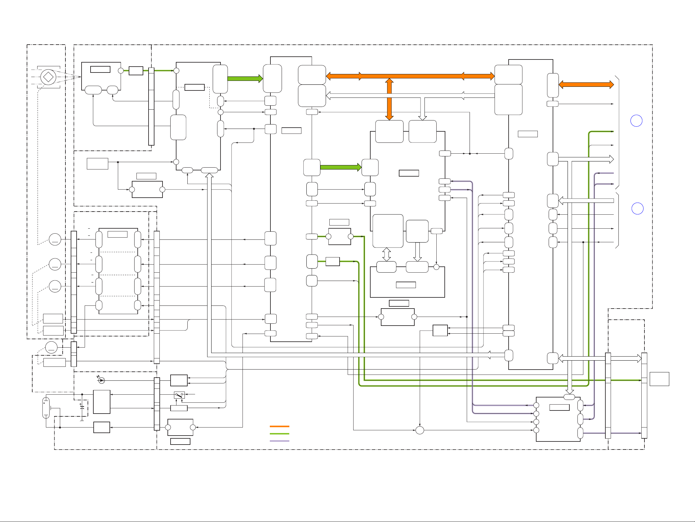
BLOCK DIAGRAMS
BLOCK DIAGRAMS
LEVEL 2
DSC-M1
US Model
Canadian Model
Australian Model
Chinese Model
E Model
Tourist Model
Hong Kong Model
Korea Model
Japanese Model
PRINTED WIRING BOARDS
PRINTED WIRING BOARDS
SERVICE NOTE
SERVICE NOTE
DISASSEMBLY
DISASSEMBLY
• For ADJUSTMENTS (SECTION 6), refer to SERVICE MANUAL, ADJ (9-876-778-51).
• For INSTRUCTION MANUAL, refer to SERVICE MANUAL, LEVEL 1 (9-876-778-41).
• Reference number search on printed wiring boards is available.
On the FP-035 FLEXIBLE, LD-175 and SY-114 board
This service manual provides the information that is premised the circuit board replacement service and not intended repair
inside the FP-035 FLEXIBLE, LD-175 and SY-114 board.
Therefore, schematic diagram, printed wiring board, waveforms, mounted parts location and electrical parts list of the
FLEXIBLE, LD-175 and SY-114 board
The following pages are not shown.
Schematic diagram .............................Pages 4-25 to 4-46
Printed wiring board ............................Pages 4-55 to 4-60
Waveforms ...........................................
are not shown.
FRAME SCHEMATIC DIAGRAMS
FRAME SCHEMATIC DIAGRAMS
SCHEMATIC DIAGRAMS
SCHEMATIC DIAGRAMS
Mounted parts location .............................
Electrical parts list ................................... Pages 5-12 to 5-16
Page 4-62
REPAIR PARTS LIST
REPAIR PARTS LIST
Page 4-64
FP-035
DIGITAL STILL CAMERA
DSC-M1
9-876-778-31
Sony EMCS Co.
2005D1600-1
©2005.04
Published by DI Technical Support Section
Page 2

SPECIFICATIONS
x Camera
[System]
Image device
Total pixels number of camera
Effective pixels number of camera
Lens Carl Zeiss Vario-Tessar
Exposure control
White balance
File format (DCF compliant)
Recording media
Flash Recommended distance (ISO set to
7.66 mm (1/2.4 type) color CCD
Primary color filter
Approx. 5 255 000 pixels
Approx. 5 090 000 pixels
3 zoom lens
f = 6.7 – 20.1 mm (38 – 114 mm
converted to a 35 mm still camera)
F3.5 – 4.4
Automatic exposure, Scene
(9 modes)
Automatic, Daylight, Cloudy,
Fluorescent, Incandescent, Flash
Still images: Exif Ver. 2.2 JPEG
compliant, DPOF compatible
Movies: MPEG4 compli
“Memory Stick Duo”
Auto):
0.3 m to 1.8 m (11 7/8 inches to
70 7/8 inches) (W)
0.5 m to 1.7 m (19 3/4 inches to
67 inches) (T)
when
selection
ant (Stereo)
[Input and Output connectors]
Multi connector
USB communication
Hi-Speed USB (USB 2.0 compli
[LCD screen]
LCD panel
Total number of dots
6.2 cm (2.5 type) TFT drive
123 200 (560×220) dots
[Power, general]
Used battery pack
Power requirements
NP-FT1
3.6 V
ant)
Power consumption (during normal
shooting)
Operating temperature
Storage temperature
Dimensions
Mass Approx. 220 g (8 oz) (including
Microphone
Speaker Piezoelectric speaker
Exif Print Compatible
PRINT Image Matching II
PictBridge
1.4 W
0°C to +40°C (+32°F to +104°F)
–20°C to +60°C (–4°F to +140°F)
51.0×114.0×27.8 mm
(2 1/8×45/8×1 1/8 inches)
(W/H/D, excluding maximum
protrusions)
battery pack NP-FT1, “Memory St ick
Duo” and wrist strap)
Electret condenser microphone
Compatible
Compatible
x UC-MA Cyber-shot Station
[Input and Output connectors]
A/V OUT (STEREO) jack (Stereo)
USB jack B
USB connection
DC IN jack
Camera connector
Minijack
Video: 1 Vp-p, 75 Ω, unbalanced,
sync negative
Audio: 327 mV (at a 47 kΩ load)
Output impedance 1 kΩ
High-Speed USB
(USB 2.0 High-Speed compatible)
x AC-LM5/LM5A AC Adaptor
Input rating
100 V to 240 V AC,
50/60 Hz
AC-LM5
10 W
AC-LM5A
11 W
Output rating
Operating temperature
Storage temperature
Dimensions
Mass AC-LM5
4.2 V DC, 1.5 A
0°C to +40°C (+32°F to +104°F)
–20°C to +60°C (–4°F to +140°F)
AC-LM5
Approx. 47×30×80 mm
(1 7/8×1 3/16×3 1/4 inches)
AC-LM5A
Approx. 48×29×81 mm
(1 15/16×1 3/16×3 1/4 inches)
(W/H/D, excluding projecting parts)
Approx. 170 g (6.0 oz)
AC-LM5A
Approx. 160 g (5.6 oz)
excluding power cord (mains lead)
x NP-FT1 battery pack
Used battery
Maximum voltage
Nominal voltage
Capacity 2.4 Wh (680 mAh)
Lithium-ion battery
DC 4.2 V
DC 3.6 V
x Accessories
AC-LM5/LM5A AC Adaptor (1)
Power cord (mains lead) (1)
Cyber-shot Station UC-MA (1)
NP-FT1 battery pack (1)
Battery case (1)
USB cable (1)
A/V connecting cable (1)
Wrist strap (1)
“Memory Stick Duo” (32 MB) (1)
Memory Stick Duo Adaptor (1)
CD-ROM (USB driver SPVD-012) (1)
Operating instructions (1)
Design and specifications are subject to change
without notice.
DSC-M1
— 2 —
Page 3

SAFETY CHECK-OUT
After correcting the original service problem, perform the following
safety checks before releasing the set to the customer.
1. Check the area of your repair for unsoldered or poorly-soldered
connections. Check the entire board surface for solder splashes
and bridges.
2. Check the interboard wiring to ensure that no wires are
"pinched" or contact high-wattage resistors.
3. Look for unauthorized replacement parts, particularly
transistors, that were installed during a previous repair . Point
them out to the customer and recommend their replacement.
4. Look for parts which, through functioning, show obvious signs
of deterioration. Point them out to the customer and
recommend their replacement.
5. Check the B+ voltage to see it is at the values specified.
6. Flexible Circuit Board Repairing
• Keep the temperature of the soldering iron around 270˚C
during repairing.
• Do not touch the soldering iron on the same conductor of the
circuit board (within 3 times).
• Be careful not to apply force on the conductor when soldering
or unsoldering.
SAFETY-RELATED COMPONENT WARNING!!
COMPONENTS IDENTIFIED BY MARK 0 OR DOTTED LINE WITH
MARK 0 ON THE SCHEMATIC DIAGRAMS AND IN THE PARTS
LIST ARE CRITICAL TO SAFE OPERATION. REPLACE THESE
COMPONENTS WITH SONY PARTS WHOSE PART NUMBERS
APPEAR AS SHOWN IN THIS MANUAL OR IN SUPPLEMENTS
PUBLISHED BY SONY.
Unleaded solder
Boards requiring use of unleaded solder are printed with the leadfree mark (LF) indicating the solder contains no lead.
(Caution: Some printed circuit boards may not come printed with
the lead free mark due to their particular size.)
: LEAD FREE MARK
Unleaded solder has the following characteristics.
• Unleaded solder melts at a temperature about 40°C higher than
ordinary solder.
Ordinary soldering irons can be used but the iron tip has to be
applied to the solder joint for a slightly longer time.
Soldering irons using a temperature regulator should be set to
about 350°C.
Caution: The printed pattern (copper foil) may peel away if the
heated tip is applied for too long, so be careful!
• Strong viscosity
Unleaded solder is more viscous (sticky, less prone to flow) than
ordinary solder so use caution not to let solder bridges occur such
as on IC pins, etc.
• Usable with ordinary solder
It is best to use only unleaded solder but unleaded solder may
also be added to ordinary solder.
ATTENTION AU COMPOSANT AYANT RAPPORT
À LA SÉCURITÉ!
LES COMPOSANTS IDENTIFÉS PAR UNE MARQUE 0 SUR LES
DIAGRAMMES SCHÉMATIQUES ET LA LISTE DES PIÈCES SONT
CRITIQUES POUR LA SÉCURITÉ DE FONCTIONNEMENT. NE
REMPLACER CES COMPOSANTS QUE PAR DES PIÈSES SONY
DONT LES NUMÉROS SONT DONNÉS DANS CE MANUEL OU
DANS LES SUPPÉMENTS PUBLIÉS PAR SONY.
CAUTION :
Danger of explosion if battery is incorrectly replaced.
Replace only with the same or equivalent type.
DSC-M1
— 3 —
Page 4

TABLE OF CONTENTS
1. SERVICE NOTE ........................................................1-1
2. DISASSEMBLY
2-1. DISASSEMBLY ······························································2-1
2-2. SERVICE POSITION ·····················································2-7
2-3. CIRCUIT BOARDS LOCATION ·································2-10
2-4. FLEXIBLE BOARDS LOCATION ······························2-11
HELP (List of caution points is shown here.)
3. BLOCK DIAGRAMS
3-1. OVERALL BLOCK DIAGRAM (1/2) ···························3-1
3-2. OVERALL BLOCK DIAGRAM (2/2) ···························3-3
3-3. POWER BLOCK DIAGRAM (1/2)································3-5
3-4. POWER BLOCK DIAGRAM (2/2)································3-7
4. PRINTED WIRING BOARDS AND
SCHEMATIC DIAGRAMS
4-1. FRAME SCHEMATIC DIAGRAM································4-1
4-2. SCHEMATIC DIAGRAMS
• FLASH UNIT (FL80000) (FLASH)
SCHEMATIC DIAGRAM ······························4-5
• FP-036 FLEXIBLE (MULTI CONNECTOR)
SCHEMATIC DIAGRAM ······························4-7
• FP-037 FLEXIBLE (CCD IMAGER)
SCHEMATIC DIAGRAM ······························4-9
• FP-039 FLEXIBLE (BATTERY)
SCHEMATIC DIAGRAM ····························4-11
• FP-040 FLEXIBLE (LITHIUM BATTERY)
SCHEMATIC DIAGRAM ····························4-12
• MS-252 (MS I/O, CONNECTOR)
SCHEMATIC DIAGRAM ····························4-13
• FP-038 FLEXIBLE (RELAY)
SCHEMATIC DIAGRAM ····························4-13
• FP-041 FLEXIBLE (LCD O/T SWITCH)
SCHEMATIC DIAGRAM ····························4-13
• CONTROL SWITCH BLOCK (PB80000)
SCHEMATIC DIAGRAM ····························4-15
• MOTOR UNIT (PI (SENSOR) BOARD) (PI SENSOR)
SCHEMATIC DIAGRAM ····························4-16
• PM-045 (1/2) (LCD PANEL DRIVE)
SCHEMATIC DIAGRAM ····························4-17
• PM-045 (2/2) (MIC AMP)
SCHEMATIC DIAGRAM ····························4-19
• CONTROL SWITCH BLOCK (PW80000) (1/2)
(FUNCTION KEY)
SCHEMATIC DIAGRAM ····························4-21
• CONTROL SWITCH BLOCK (PW80000) (2/2)
(CONNECTOR)
SCHEMATIC DIAGRAM ····························4-23
4-3. PRINTED WIRING BOARDS
• FP-036 FLEXIBLE (MULTI CONNECTOR)
PRINTED WIRING BOARD ·······················4-49
• FP-037 FLEXIBLE (CCD IMAGER)
PRINTED WIRING BOARD ·······················4-49
• FP-038 FLEXIBLE (RELAY)
PRINTED WIRING BOARD ·······················4-50
• FP-041 FLEXIBLE (LCD O/T SWITCH)
PRINTED WIRING BOARD ·······················4-50
• MS-252 (MS I/O, CONNECTOR)
PRINTED WIRING BOARD ·······················4-51
• FP-040 FLEXIBLE (LITHIUM BATTERY)
PRINTED WIRING BOARD ·······················4-51
• PM-045 (LCD PANEL DRIVE, MIC AMP)
RINTED WIRING BOARD ·························4-53
Printed wiring board of the FP-035, LD-175 and
SY-114 board are not shown.
Pages from 4-55 to 4-60 are not shown.
4-4. WAVEFORMS ······························································4-61
Waveforms of the SY-114 board are not shown.
Page 4-62 is not shown.
4-5. MOUNTED PARTS LOCATION ·································4-63
Mounted parts location of the SY-114 board is not
shown.
Page 4-64 is not shown.
5. REPAIR PARTS LIST
5-1. EXPLODED VIEWS ······················································ 5-1
5-1-1.OVERALL SECTION·····················································5-3
5-1-2.BATTERY HOLDER SECTION ····································5-4
5-1-3.LCD SECTION-1 ····························································5-5
5-1-4.LCD SECTION-2 ····························································5-6
5-1-5.LENS SECTION ·····························································5-7
5-2. ELECTRICAL PARTS LIST ··········································5-9
Electrical parts list of the FP-035, LD-175 and SY-114
board are not shown.
Pages from 12 to 5-16 are not shown.
DSC-M1
Shematic diagram of the FP-035, LD-175 and SY-114
board are not shown.
Pages from 4-25 to 4-46 are not shown.
— 4 —
Page 5
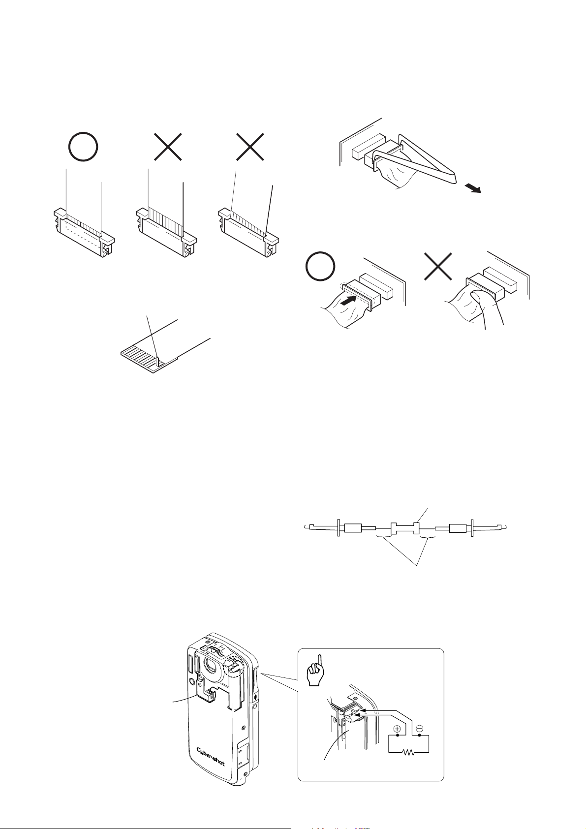
• NOTE FOR REPAIR
1. SERVICE NOTE
Make sure that the flat cable and flexible board are not cracked of
bent at the terminal.
Do not insert the cable insufficiently nor crookedly.
Cut and remove the part of gilt
which comes off at the point.
(Take care that there are
some pieces of gilt left inside)
When remove a connector, don't pull at wire of connector.
Be in danger of the snapping of a wire.
When installing a connector, don't press down at wire of connector.
Be in danger of the snapping of a wire.
[Discharging of the FLASH unit’s charging capacitor]
The charging capacitor of the FLASH unit is charged up to the
maximum 300 V potential.
There is a danger of electric shock by this high voltage when the
capacitor is handled by hand. The electric shock is caused by the
charged voltage which is kept without discharging when the main
power of the DSC-M1 is simply turned off. Therefore, the remaining
voltage must be discharged as described below.
Preparing the Short Jig
To preparing the short jig. a small clip is attached to each end of a
resistor of 1 kΩ /1 W (1-215-869-11)
Wrap insulating tape fully around the leads of the resistor to prevent
electrical shock.
Discharging the Capacitor
Short circuits between the positive and the negative terminals of
charged capacitor with the short jig about 10 seconds.
1 kΩ/1 W
Wrap insulating tape.
Caution
DSC-M1
Flash unit
1-1
Capacitor
Shorting jig
(1k
Ω
/ 1w)
Page 6
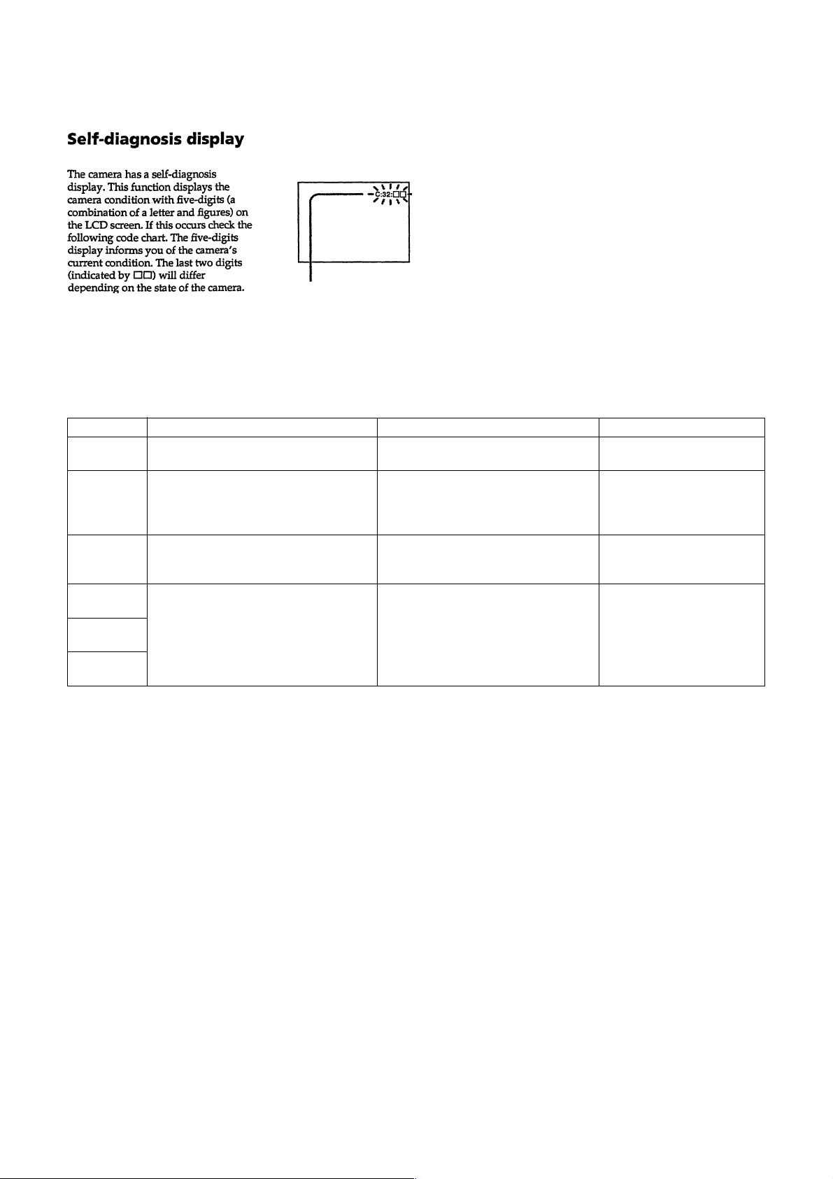
[Description on Self-diagnosis Display]
Self-diagnosis display
• C: ss: ss
The contents which can be handled
by customer, are displayed.
• E: ss: ss
The contents which can be handled
by engineer, are displayed.
Display Code
C:32:01
C:13:01
E:91:01
E:01:XX
E:61:00 *1
E:61:10 *1
Note : The error code is cleared if the battery is removed, except defective flash unit.
*1: The error display is given in two ways.
Turn off the main power then back on.
Replace the memory stick.
Format the memory stick with the DSC-M1.
Checking of flash unit or replacement of
flash unit.
Checking of lens drive circuit
Countermeasure
Trouble with hardware.
• The type of memory stick that cannot be
used by this machine, is inserted.
• Data is damaged.
• Unformatted memory stick is inserted.
Abnormality when flash is being
charged.
When failed in the focus initialization.
Cause
Caution Display During Error
SYSTEM ERROR
MS ERROR
Flash LED
Flash display
Flashing at 3.2 Hz
—
DSC-M1
1-2E
Page 7
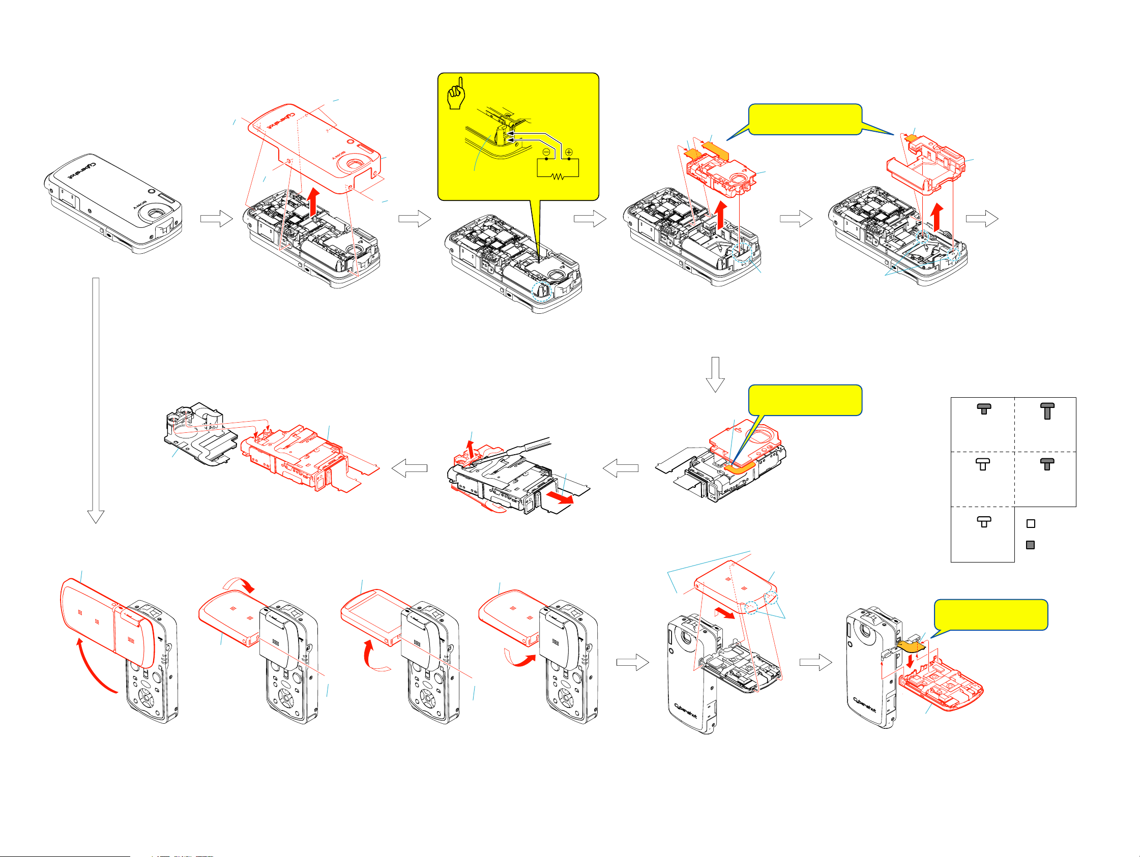
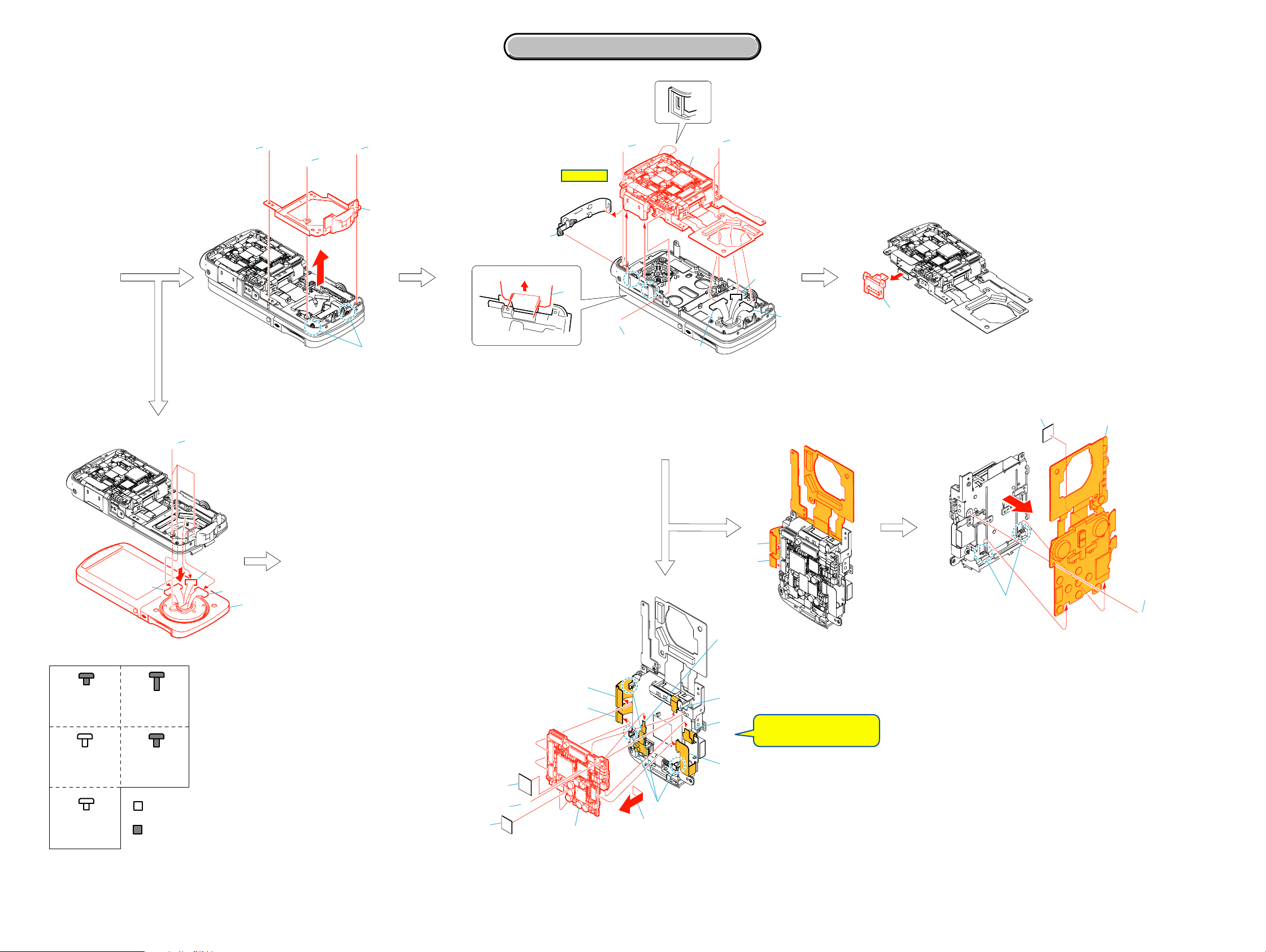
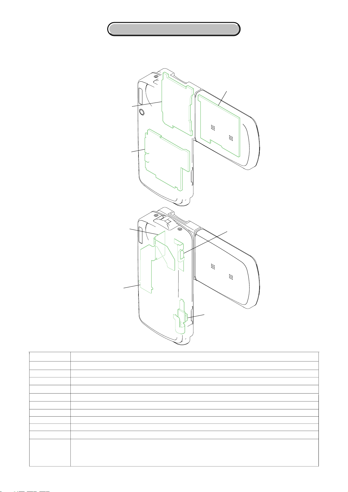
The following flow chart shows the disassembly procedure.
2-1. DISASSEMBLY
2. DISASSEMBLY
B
3
A
2
1
Two screws (M1.7x3) black
2
Screw (M1.7x3) black
3
Screw (M1.7x5) black
4
A
A
4
Two screws (M1.7x3) black
5
Cabinet (Front) assembly
Caution
Note: Be very careful not to
1
2
5
Capacitor
1
Discharging the capacitor
1
Shorting jig
Ω
/ 1W)
(1k
1
FP-035 flexble board (25P)
2
FP-037 flexble board (33P)
(From the CCD block assembly)
damage the flexible board.
4
3
3
Two claws
4
Lens section
1
1
2
3
2
3
Battery holder section,
(See page 2-3, 2-4)
Two claws
Flash unit (FL80000) (16P)
Flash unit (FL80000), ST frame (Upper), ST frame (Lower)
Note: Be very careful not to
damage the flexible board.
1
1
Motor unit (11P)
1
1
Motor unit, Lens barrier holder
2
Lens section
2
1
Push this portion with a driver
in the direction of the arrow a.
1
a
2
b
2
Remove the lens section
in the direction of the arrow b.
A
1
b
4
6
1
3
A
Screw
M1.7x3
2-515-483-21
C
Screw
M2x4
2-080-204-01
E
Screw
M1.7x3
2-515-488-21
B
Screw
M1.7x5
2-515-483-41
D
Tapping screw
M1.7x3.5
2-080-204-01
Silver
Black
A
a
a
2
A
c
d
A
2
Note: Be very careful not to
damage the flexible board.
4
f
DSC-M1
1
Turn over the LCD section in the direction of the arrow a.
2
Turn over the LCD section in the direction of the arrow b.
3
Screw (M1.7x3) black
3
4
Turn over the LCD section in the direction of the arrow c.
5
Screw (M1.7x3) black
6
Turn over the LCD section in the direction of the arrow d.
5
1
Two screws (M1.7x3) black
2
Two claws
3
Remove the P cabinet (C) assembly
in the direction of the arrow a.
2-1 2-2
5
4
FP-038 flexible board (29P)
5
Remove the P cabinet (M) assembly,
LCD, etc. in the direction of the arrow f.
Page 8
2. DISASSEMBLY
2. DISASSEMBLY
C
E
1
C
3
D
2
HELP 01
5
8
7
E
6
9
E
5
4
1
Screw (M1.7x3) silver
2
Tapping screw (M1.7x3.5) black
3
Screw (M2x4) silver
4
4
Two claws
5
Lens frame assembly
1
Harness (PD-130) (20P)
2
Harness (MA-154) (10P)
3
Harness (MS-121) (12P)
4
Two tapping screws (M1.7x3.5) black
5
Screw (M1.7x3) silver
6
Screw (M1.7x3) silver
1
4
D
2
3
Remove the multi holder assembly
7
in the direction of the arrow.
8
BT cover, BT arm
9
Battery holder section,
Multi holder assembly
1
Multi holder assembly
1
3
4
A
Screw
M1.7x3
2-515-483-21
C
Screw
M2x4
2-080-204-01
E
Screw
M1.7x3
2-515-488-21
1
B
Screw
M1.7x5
2-515-483-41
D
Tapping screw
M1.7x3.5
2-080-204-01
Silver
Black
1
Harness (PD-130) (20P)
2
Harness (MA-154) (10P)
3
Harness (MS-121) (12P)
4
Three screws (M2x4) silver
5
LCD section
1
2
3
5
Lens section (See page 2-5, 2-6)
1
FP-039 flexible board (11P)
2
Control switch block (PW80000) (39P)
3
Control switch block (PW80000) (19P)
4
FP-036 flexible board (19P)
5
Screw (M1.7x3) silver
6
Three claws
7
Remove the SY board
in the direction of the arrow.
8
FP-040 flexible board (6P)
9
FP-036 flexible board (6P)
0
SY radiation sheet
qa
Radiation sheet
qs
SY board
0
A
5
qa
2
3
qs
6
7
2
2
1
E
8
1
9
4
1
Control switch block (PW80000) (39P)
2
Control switch block (PW80000) (19P)
Note: Be very careful not to
damage the flexible board.
1
Screw (M1.7x3) silver
2
Two claws
3
Radiation sheet
4
Control switch block (PW80000)
DSC-M1
2-3 2-4
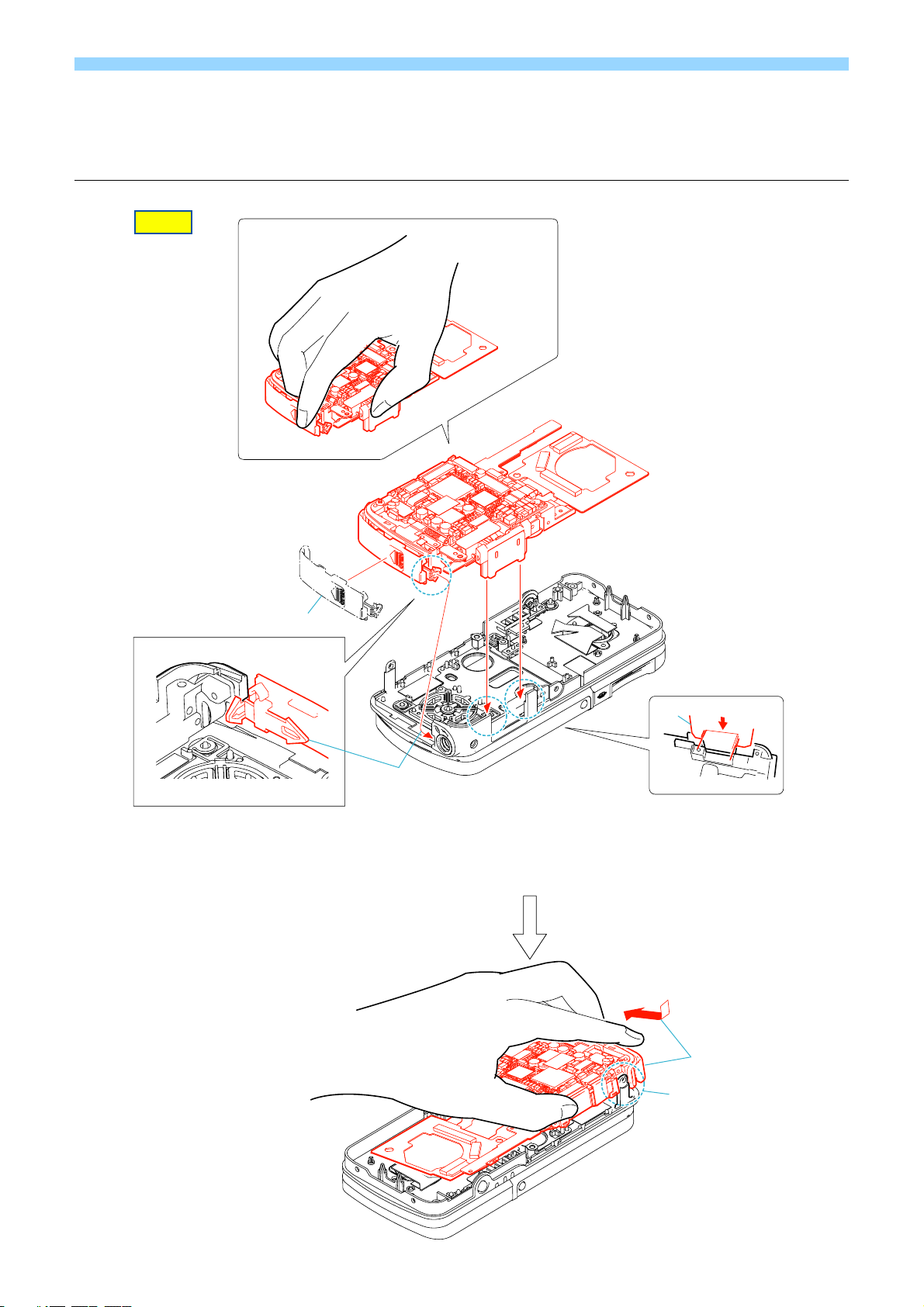
Page 9
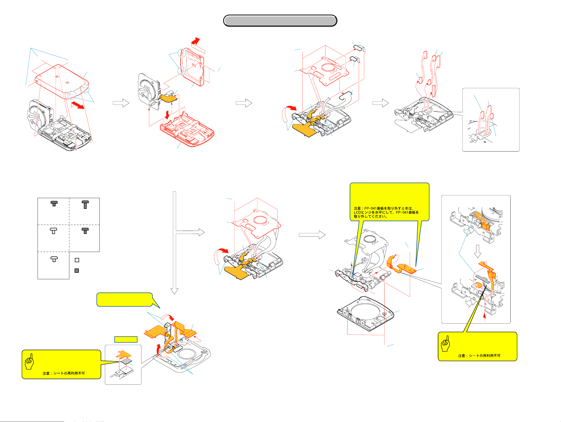
2. DISASSEMBLY
2. DISASSEMBLY
1
A
A
1
Four screws (M1.7x3) black
2
Two claws
3
Remove the P cabinet (C) assembly
in the direction of the arrow.
A
b
E
4
3
1
5
2
1
FP-038 flexible board (29P)
2
Remove the P cabinet (M) assembly,
LCD, etc. in the direction of the arrow a.
3
Two screws (M1.7x3) black
a
2
3
A
4
Two claws
5
Remove the hinge cover,
MS holder assembly, etc. in the
direction of the arrow b.
2
8
4
1
1
Turn over the LCD hinge assembly
in the direction of the arrow.
2
Three screws (M1.7x3) silver
3
FP-038 flexible board (31P)
4
FP-041 flexible board (6P)
3
7
6
5
5
Harness (PD-130) (20P)
6
Harness (MA-154) (10P)
7
Harness (MS-121) (12P)
8
MS-252 board, Piezoelectric buzzer, etc.
2
1
1
Harness (PD-130) (20P)
2
Harness (MA-154) (10P)
3
3
Harness (MS-121) (12P)
Harness (MS-121)
Harness (PD-130)
Harness (MA-154)
A
Screw
M1.7x3
2-515-483-21
C
Screw
M2x4
2-080-204-01
E
Screw
M1.7x3
2-515-488-21
B
Screw
M1.7x5
2-515-483-41
D
Tapping screw
M1.7x3.5
2-080-204-01
Silver
Black
Note: Be very careful not to
damage the flexible board.
3
Note: To remove this FP-041 flexible board,
be sure to turn the LCD hinge to level, and then
2
E
5
4
remove this FP-041 flexible board.
(Japanese)
3
Bottom side
E
4
5
1
1
Turn over the LCD hinge assembly
in the direction of the arrow.
2
Three screws (M1.7x3) silver
a
2
3
3
FP-038 flexible board (31P)
4
FP-041 flexible board (6P)
5
MS-252 board,
Piezoelectric buzzer, etc.
2
DSC-M1
Caution
Note : The sheet cannot be reused.
(Japanese)
HELP 02
1
1
b
1
4
Peel off the hinge adhesive sheet (Upper).
2
FP-038 flexible board (31P)
3
Turn over the LCD hinge assembly
in the direction of the arrow a.
4
Remove the FP-038 flexible board
in the direction of the arrow b.
1
Two screws (M1.7x3) black
2
Hinge cabinet
3
Screw (M1.7x3) silver
4
Peel off the hinge adhesive sheet (Lower).
5
FP-041 flexible board
A
2-5 2-6
Caution
Note : The sheet cannot be reused.
(Japanese)
Page 10
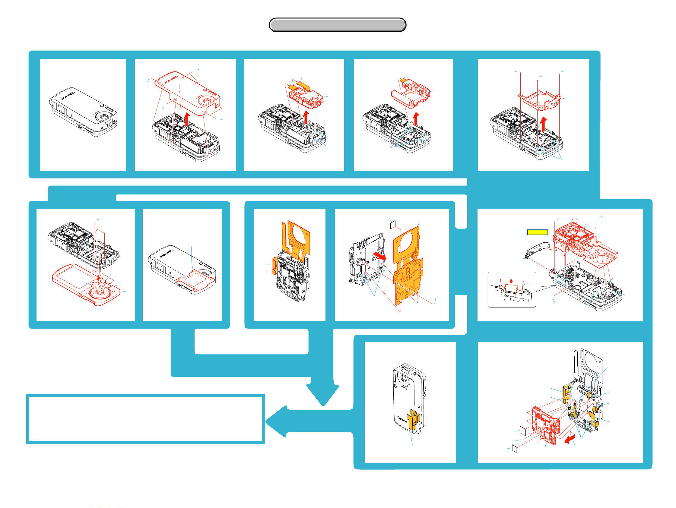
2-2. SERVICE POSITION
2. DISASSEMBLY
2. DISASSEMBLY
C
4
A
B
3
5
1
2
4
2
3
E
1
C
3
D
2
5
A
2
1
A
3
4
MS-252 board
1
4
3
4
HELP 01
E
6
4
D
9
2
1
3
5
[SERVICE POSITION TO CHECK THE VTR SECTION]
Connection to Check the VTR Section (page 2-9)
1
2
2
1
E
FP-036 flexible board
8
2
7
E
5
2
3
0
A
5
qa
qs
1
6
7
3
8
1
9
4
DSC-M1
2-7 2-8
Page 11
2. DISASSEMBLY
2. DISASSEMBLY
[SERVICE POSITION TO CHECK THE SY-114 BOARD]
Harness
(MA-154) (10P)
LCD section
Harness
(PD-130) (20P)
MS-252 board
Control switch block
(PW80000)
CN003
CN001
FP-035 flexible board
(25P)
PW80000 (39P)
CN702
PW80000 (19P)
SY-114 board
CN751
CN752
CN703
CN707
CN701
CN704
FP-036 flexible board
(19P)
FP-036 flexible board
AC IN
AC power
adaptor
DC-IN
Note1: When checking the VIDEO AMP (SY-114 board IC302)
or the USB circuit, connect the Syber-shot station (UC-MA).
CN002
Harness
(MS-121) (12P)
FP-037 flexible board
(33P)
FP-036 flexible board
(6P)
Flash unit
(FL80000)
(16P)
Caution
Lens section
Flash unit
Discharging the capacitor
DSC-M1
Syber-shot station
UC-MA (1-818-873-11)
DC IN jack
To DC IN jack
A/V OUT jack
USB connector
USB connector
(1-827-754-21)
AC power
adaptor
AC IN
2-9
Capacitor
Shorting jig
(1k
Ω
/ 1W)
Page 12
2. DISASSEMBLY
2. DISASSEMBLY
2-3. CIRCUIT BOARDS LOCATION
The flexible boards contained in the lens block are not shown.
MS-252
SY-114
PM-045
NAME
FP-035
FP-036
FP-037
FP-038
FP-039
FP-040
FP-041
LD-175
MS-252
PM-045
SY-114
LD-175
FP-035
FP-036
FUNCTION
LENS DRIVE/BARRIER IF, LED DRIVE
MULTI CONNECTOR
CCD IMAGER
RELAY
BATTERY
LITHIUM BATTERY
LCD O/T SWITCH
LENS DRIVE
MS I/O, CONNECTOR
LCD PANEL DRIVE, MIC AMP
CAMERA A/D CONV., TIMING GENERATOR, CAMERA DSP, LENS CONTROL,
CAMERA SYSTEM CONTROL, DIGITAL SIGNAL PROCESS, HI CONTROL, AUDIO I/O,
DC/DC CONVERTER, CONNECTOR, FLASH DRIVE, CONNECTOR
FP-041
DSC-M1
2-10
Page 13
2. DISASSEMBLY
2. DISASSEMBLY
2-4. FLEXIBLE BOARDS LOCATION
The flexible boards contained in the lens block are not shown.
CONTROL SWITCH BLOCK
(PW80000)
CONTROL SWITCH BLOCK
(PB80000)
NAME
FP-035
FP-036
FP-037
FP-038
FP-039
FP-040
FP-041
LD-175
MS-252
PM-045
SY-114
FP-038
FP-037
FP-039
FP-040
FUNCTION
LENS DRIVE/BARRIER IF, LED DRIVE
MULTI CONNECTOR
CCD IMAGER
RELAY
BATTERY
LITHIUM BATTERY
LCD O/T SWITCH
LENS DRIVE
MS I/O, CONNECTOR
LCD PANEL DRIVE, MIC AMP
CAMERA A/D CONV., TIMING GENERATOR, CAMERA DSP, LENS CONTROL,
CAMERA SYSTEM CONTROL, DIGITAL SIGNAL PROCESS, HI CONTROL, AUDIO I/O,
DC/DC CONVERTER, CONNECTOR, FLASH DRIVE, CONNECTOR
DSC-M1
2-11E
Page 14
HELP 01
1
BT cover, BT arm
2
Multi holder assembly
3
BT arm
4
Claw
5
Aaaemble or install the Battery holder section, etc.
in the direction of the arrow.
1
4
3
2
5
HELP
Sheet attachment positions and procedures of processing the flexible boards/harnesses are shown.
DSC-M1
HELP
Page 15
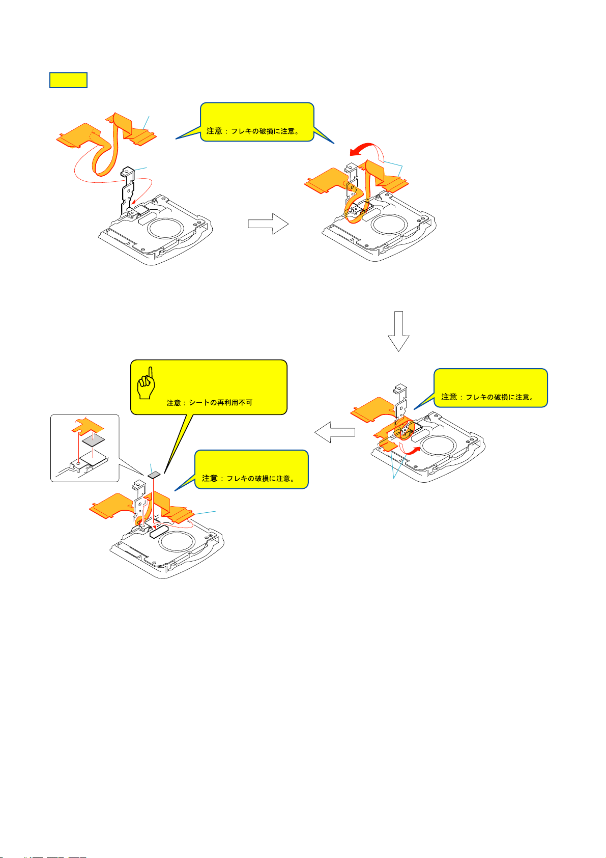
HELP 02
2
1
LCD hinge assembly
1
2
FP-038 flexible board
Note: Be very careful not to
damage the flexible board.
Caution
Note : The sheet cannot be reused.
3
3
Twist the FP-038 flexible board.
Note: Be very careful not to
damage the flexible board.
5
5
Hinge adhesive sheet (upper)
6
FP-038 flexible board (31P)
Note: Be very careful not to
damage the flexible board.
4
4
6
Twist the FP-038 flexible board.
DSC-M1
HELP
Page 16

Link
Link
3. BLOCK DIAGRAMS
OVERALL BLOCK DIAGRAM (1/2)
OVERALL BLOCK DIAGRAM (1/2)
OVERALL BLOCK DIAGRAM (2/2) POWER BLOCK DIAGRAM (2/2)
POWER BLOCK DIAGRAM (1/2)
POWER BLOCK DIAGRAM (1/2)
POWER BLOCK DIAGRAM (2/2)OVERALL BLOCK DIAGRAM (2/2)
DSC-M1
Page 17
3. BLOCK DIAGRAMS
3-1. OVERALL BLOCK DIAGRAM (1/2)
LENS UNIT
IRIS
SHUTTER
ZOOM RESET
SENSOR
FOCUS RESET
SENSOR
LENS
BARRIER
MOTOR
LENS BARRIER
OPEN SENSOR
LENS UNIT
PI (SENSOR)
BOARD
XENON
TUBE
IRIS
MOTOR
M
ZOOM
MOTOR
M
FOCUS
MOTOR
M
M
PH001
FLASH UNIT (FL80000)
CCD BLOCK ASS'Y
FP-037 (FLEXIBLE BOARD)
IC001
CCD IMAGER
1-5,7,8,9
11-14
54MHz
XTAL OSC
V1A,V1B
V2
V3A,V3B
V4
V5A,V5B
V6
V7A,V7B
V8
X151
24-20
LD-175 BOARD
CN002
IRIS A
IRIS A
IRIS B
19
18
21
20
13
12
14
15
8
10
11
9
2
5
4
|
1
5
6
C901
MAIN
CAPACITOR
XE K(L)
CN501
XE A(H)
G4
H4
G5
IRIS MOTOR
H6
DRIVE
C1
ZOOM MOTOR
D2
DRIVE
E1
E2
A6
FOCUS MOTOR
B5
DRIVE
A4
B4
LENS BARRIER
E7
MOTOR DRIVE
D7
IC001
IRIS B
ZOOM A
ZOOM A
ZOOM B
ZOOM B
FOCUS A
FOCUS A
FOCUS B
FOCUS B
LENSV OUTA
LENSV OUTB
FP-035
(FLEXIBLE BOARD)
LENSV OPEN SENS
D003
(AF LED)
Q001, T002
HIGH
VOLTAGE
CHARGER
Q004
FLASH
DRIVE
17
Q004
BUFFER
H1A,H1B
H2A,H2B
RG
AF LED K
STB UNREG
STB FULL
IGBT ON
4
13
12
10
9
7
19
|
23
25
26
27
29
|
32
CK
(1/9)
IC152
FREQUENCY
DEVIDER
G1
H2
G2
G3
B3
B2
A2
A1
C8
B8
C7
B7
F7
F8
CN701
9
7
8
15
13
14
12
10
11
5
4
16
19
1
1
16
|
12
4
3
CCD OUT
( ) : Number in parenthesis ( ) indicates the division number of schematic diagram where the component is located.
SY-114 BOARD (1/2)
HR EN3
HR DIR3A
HR DIR3B
HR EN0
HR DIR0A
HR DIR0B
HR EN2
HR DIR2A
HR DIR2B
STRB ON
Y13, AB13
Y14, AA13
AB14, Y15
AB15, AA14
AA15, Y16
AB16, AA16
AB17, AA17
AA18
Y18
AC16
Y17
AB18
N21
L21
P21
K20
L22
J21
M21
M20
N20
F20
F21
AB4
CAM SO, SCK
U4, V3, V2, W1
V4, W2, W4, Y4
Y2, AA1, W3, AA2
Y3, AA3, AC1, AB2
J3, L2, L4, L1, K3
L3, M2, M4, M3, N2
N3, P2, N4, P4, P3
R1, R3, R2, T3, T1
R4, T2, T4, U2, U3
T23
(2/9)
IC301
CAMERA
DSP
B21, D19
C20, B20
A20, D18
C19, B19
D22
C22
D20
B22
F23
E23
C23
D23
C18
D17
AC3
AC12
T20
VIDEO/AUDIO SIGNAL
VIDEO SIGNAL
AUDIO SIGNAL
MC D0 - MC D15
MC A1 - MC A25 MC A1 - MC A25
MC CKIO
(4/9)
IC101
CODEC
IC102
C3, A2, D4, B3, A3
D5, D6, C5, B5, A5
H8, C6, B6, D7, A7
G8, D8, B8, C8, G9
B9
MC A1 - MC A21
A0 - A11,
A13,A14
U19, T18, V20
U18, W20, Y21
N14, P15, AA21
Y20, W19, AA20
Y19, AA19
26-28,63-69
25,22,24,23
A0 - A11,
BA1,BA0
(4/9)
YO
RO
GO
BO
HD0
PANEL V
YC0 - YC7
HD
VD
FLD
FCK27
IC302
4
Q302-304
BUFFER
(2/9)
VIDEO
AMP
PANEL R
PANEL G
PANEL B
H9, D10, C10, G10
H10, A11, C11, C12
D12, H11, B12, A13
C13, D13, B13, G12
MC D0 - MC D15
AA3, W4
Y3, AA2
P9, R8
AA1, Y2
P11
V10
W10
AA9
DQ0 - DQ31
U20, U18, U21, U19
K20, U14, K18, K19
K15, K14, L21, L19
M19, M18, L14, M20
V OUT
2
N21, N19, N18, N20
M15, P19, P20, R21
R20, R19, R18, T20
T19, U21, N15, U20
3-14,77-88
32-43,48-59
DQ0 - DQ31
SDRAM
(2/9)
IC303
ADCK
AOUT
XSYS RST
FREQUENCY
1
DEVIDER
ADA ADCK
5
BEEP
+
51
HR EN3
HR DIR3A
HR DIR3B
HR EN0
HR DIR0A
HR DIR0B
HR EN2
HR DIR2A
HR DIR2B
LENSV ENB
LENSV DIR
XZM RST SENS
XFC RST SENS
CN702
CN707
Q653
2 4
86
37
42
48
51
33
10, 13
113, 17
20, 109
112, 115
125, 119
118, 121
84
Q703
LED
DRIVE
Q651,652
SW
IGBT
DRIVE
IC651
S/H
(1/9)
IC151
TIMING
GENERATOR
123,3
(8/9)
134,136
126-129
XCAM RST
PRELAMP AF CONT
SELF TIMER LED
ST UNREG
STRB CHRG
XSTRB FULL
STRB ON
2, 4
6, 9
12, 15
18, 21
24, 27
30, 32
64
55
99
49
66
101
120
EXT CLK
CA AD0 - CA AD13
CLP DM
CLP OB
MCK TG
CA HD
CAM F
CAM F
XZM RST SENS1
XFC RST SENS
SDR CLK
G21
71
CLK
Q501
MOD
W14
L21, L23, M24,K23
MC D0 - MC D15
H22, J21, J22, F24
K21, H21, M23, K22
G21, L24, F23, E23
V22, V21, V23, R22
W22, J22, W21, T22
R23, N21, P22, P21
P23, R21, M22, T21
P24, J21, J23, N22
J24, N23, T24, M21
T23
(3/9)
IC501
CAMERA
AD19
AC15
H23
C23
AC12
AB7
AD14
SYSTEM
A7
CONTROL
H1
G3
B6
B1
F21
F1
A6
MC CKIO
ADA SOA
C2
ADA SIA
H7
ADA ADCK
D2
STRB CHRG
XSTRB FULL
LENSV ENB
LENSV DIR
LENSV OPENSENS
PRELAMP AF CONT
SELF TIMER LED
XCAM RST
CAM F
EXT CLK
MELODY ENV
MELODY
B16
C15
A15
D15
B15
D16
C22
B11
A11
C11
D13
B13
C13
AB5
AB13
AB22
B23
D14
K2
MC MSDIO,D1-D3
MC MSBS
MC MSCLK
SYS SO, SI, SCK
FR SO, SI, SCK
XACCESS LED
PANEL R
PANEL G
PANEL B
HD0
PANEL V
MIC L
MIC R
SP+
SP-
XAE LOCK ON
XSHTR ON
PB MODE LED
REC MODE LED
XSYS RST
1
TO
OVERALL
BLOCK DIAGRAM
(2/2)
(PAGE 3-3)
TO
OVERALL
BLOCK DIAGRAM
(2/2)
(PAGE 3-3)
FP-036
(FLEXIBLE
2
BOARD)
(1/2)
CAM SO, SCK
A12
B12
ADA SOA
ADA SIA
ADA ADCK
BEEP IN
L1, M1
J1, K1
27
26
31
14
(6/9)
IC801
AUDIO
AMP
USBPHY D+, D-
SYS SO,SCK
38,35
MIC L
MIC R
71
77
SP+
SP-
17
16
2
4
CN703
16
14
2
6
4
VIDEO OUT
AUDIO L OUT
AUDIO R OUT
10
12
17
16
18
CN001
MULTH
CONNECTOR
(CRADLE)
DSC-M1
3-1 3-2
Page 18

3-2. OVERALL BLOCK DIAGRAM (2/2)
( ) : Number in parenthesis ( ) indicates the division number of schematic diagram where the component is located.
CN001
MULTH
CONNECTOR
(CRADLE)
14
11
13
24
3
1
BATTERY
TERMINAL
FP-036
(FLEXIBLE
BOARD)
(2/2)
AV JACK IN
USB JACK IN
XMULTI JACK IN
BATT/XEXT
ACV UNREG
|
FP-040
(FLEXIBLE
BOARD)
BT001
LITHIUM
BATTERY
(SECONDARY)
FP-039
(FLEXIBLE
BOARD)
S
SY-114 BOARD (2/2)
CN703
11
19
10
9
4
|
6
CN704
CN706
1
VL 3V
|
3
CN705BT901
11
BATT UNREG
|
7
BATT SIG
6
5
REG GND
|
1
Q002
TO
OVERALL
BLOCK DIAGRAM
(1/2)
(PAGE 3-2)
D013
2
F002
F003
D015
F004
D036
VL 3V
D011
D8
A10
B11
D9
E9
D1
E5
D4
E4
Q409,411
ST UNREG
ACV UNREG
BATT UNREG
3V
REG
OUT8A
OUT8B
BATTERY
CHARGER
IC001
IC002
IC003
XAE LOCK ON
XSHTR ON
REC MODE LED
PB MODE LED
XSYS RST
FR SO, SI, SCK
BATT SIG
BATTERY IN
DETECT
FET DRIVE
(7/9)
DC/DC
CONVERTER
RESET
(7/9)
(7/9)
A11
L8
K8
B7
B9
B7
D2
E3
C7
D7
EVER 3.0V
X402
32.768KHz
Q407
I/F
DDCON SO, SCK
D 1.5V
D 2.8V
A 2.8V
AU 2.8V
A 3.1V
M 5V
ST 5V
CAM 3.1V
CAM 15.0V
CAM -8.0V
PANEL 5V
PANEL 8.5V
BL LEV
BL H
BL L
D 1.2V
CAM -0.5V
Q406
FR SO
D2
FR SI
D1
XFR SCK
E1
J4
32KHz IN
32KHz OUT
J5
A3
AV JACK IN
C8
XUSB JACK IN
XMULTI JACK IN
C4
A7
BATT/XEXT
BATT SI
G2
G1
BATT SO
C1
DDCON SO
D3
DDCON SCK
XRSTX
D7
A5
BACK UP VCC
H4
A9
BATT IN
INIT CHARGE
J1
H2
FAST CHARGE
E8
SYS DD ON
XCHARGE/XSTRB LED
KEY AD2
KEY AD1
KEY AD3
KEY AD0
XPWR ON
(5/9)
IC491
HI CONTROL
XSYS RST
MS IN
XLCD OPEN SW
Q753
LED
DRIVE
Q754
LED
DRIVE
XRESET SW
CN752
CN751
16
15
4
5
7
8
9
17
10
18
3
2
29
6
4
3
5
7
2
8
9
25
26
27
CN002
XMS IN
CN003
S213
RESET
9
10
8
6
11
5
7
4
15
14
13
9
10
8
6
11
5
7
4
15
14
13
CN004
CN005
XAE LOCK ON
XSHTR ON
REC MODE LED
PB MODE LED
B1
G6
H6
J7
J6
B8
B3
B6
Q404
MC MSDIO,D1-D3
MC MSBS
MC MSCLK
XACCESS LED
PANEL R
PANEL G
PANEL B
1
TO
OVERALL
BLOCK DIAGRAM
(1/2)
(PAGE 3-2)
B7
HD0
PANEL V
SYS SO, SI, SCK
MIC L
MIC R
SP+
SP-
BL LEV
BL H
BL L
CN752
33
34
20
23
21
39
36
37
16
18
11
12
14
XLCD OPEN SW
CN001
7
6
20
17
19
11
1
4
3
3
1
10
9
7
8
7
20
17
19
11
1
4
3
3
1
10
9
7
8
6
CN003
S204
SHUTTER
D201 (REC MODE)
D203 (PB MODE)
D202 (FLASH/CHARGE)
S212
START/STOP
S210
ZOOM
S214
POWER
S215
MODE
MS-252 BOARD
Q002
LED
DRIVE
CN002
24
23
22
15
13
31
28
30
19
11
9
8
1
3
FP-038
(FLEXIBLE
BOARD)
6
5
6
1
CN006
CONTROL SWITCH
BLOCK (PW80000)
S206-209,211,216
RIGHT,SET,DOWN,LEFT
UP,X1SHOTM
S201-203,205
DISPLAY,DUST,MENU
STILL/XMIP
4,3,5,7,
2,8
6
D004(ACCESS)
7
8
9
15
Q205
LPF
17
1
4
2
11
19
21
22
29
27
24
25
CN204
(LCD TURN)
(LCD OPEN)
CN001
MEMORY
STICK
DUO
SP901
SPEAKER
PM-045 BOARD
(1/2)
34
33
IC201
32
RGB
DRIVE
48
1
45
TIMING
42
GENERATOR
44
3
31
(2/2)
14
IC301
22
MIC AMP
CN203
2
3
4
S412
S411
20
21
22
26
24
VST,VCK,EN,DWN
28
XSTBY,PCG,HST,REF
24
WIDE,HCK2,HCK1,RGT
|
20
17
|
5
35
1
S001-003
PLAY/,
PHOTO/,
MOVIE
VIDEO/AUDIO SIGNAL
VIDEO SIGNAL
AUDIO SIGNAL
BL H
BL L
COM
PSIG
R
G
B
CN201
CN202
CN302
CN301
4
5
3
24
23
6
22
|
19
14
|
11
9
|
7
BACK LIGHT
2
1
3
1
1
LCD901
COLOR
LCD UNIT
MIC
L
MIC
R
CONTROL SWITCH
BLOCK (PB80000)
FP-041
(FLEXIBLE BOARD)
LED901
MIC901
MIC902
DSC-M1
3-3 3-4
Page 19

3-3. POWER BLOCK DIAGRAM (1/2)
SY-114 BOARD (1/2)
FP-036
(FLEXIBLE
BOARD)
CN703
9
CN704
4
6
CN705
11
BATT UNREG
7
BATT SIG
6
REG GND
5
1
CB701
CN001
MULTH
CONNECTOR
(CRADLE)
TERMINAL
BT901
BATTERY
BATT/XEXT
24
3
ACV UNRG
1
S
FP-039
(FLEXIBLE
BOARD)
FP-040
(FLEXIBLE
BOARD)
BT001
LITHIUM
BATTERY
(SECONDARY)
D202
(FLASH/CHARGE)
S214
POWER
S213
RESET
CN706
1
3
CN752
3
7
8
6
VL 3V
Q409,411
Q407
I/F
XRESET SW
EVER 3.0V
CONTROL
SWITCH
BLOCK
(PW80000)
(1/2)
( ) : Number in parenthesis ( ) indicates the division number of schematic diagram where the component is located.
Q002
H8
G8
A7
G2
G1
B8
B1
BATT SENS
ACV SENS
BATT/XEXT
BATT SI
BATT SO
X PWR ON
XCHARGE/
XSTRB LED
F002
F003
D036
D015
D013
IC491
HI CONTROL
BACK UP VCC
DDCON SO
DDCON SCK
XCS DDCON
SYS DD ON
INIT CHARGE
FAST CHARGE
DD CON SENS
XSYS RST
XRSTX
BATT IN
F004
(5/9)
A5
H4
D7
A9
C1
D3
H1
E8
J1
H2
F8
B3
D 1.5V
INIT CHARGE
FAST CHARGE
L002
L001
EVER 3.0V
D011
D1
E5
D4
D2
E4
E3
D9
E9
B11
A11
A10
D8
B9
B7
A7
L8
K8
K7
C7
D7
BATTERY
CHARGER
FET
DRIVE
OUT8A
OUT8B
3V
REG
RESET
DIN
CLK
LD
SYS DD ON
IC001
DC/DC
CONVERTER
BATTERY IN
DETECT
(7/9)
VCC1A
VCC1B
VCC1C
OUT11A
OUT11B
OUT11C
OUT12A
OUT12B
OUT12C
VCH1A
VCH1B
VCH1C(FB4)
VCH7
VCC2
OUT2
VCH2
OUT3A
OUT3B
OUT3C
VCH3A(FB3)
VCH3B
VCH3C(FB6)
VCH3S
VCC GD
OUT4
VCH4
VCC5
OUT5
VCH5
OUT6
VCH6
ICH6
REF6
CBG
VLDO4
VLDO5
G11
G10
G9
H11
H10
J11
L11
K10
L10
F10
E11
J9
K9
L9
K3
F9
J3
K1
J2
J1
H4
H3
H2
H1
K6
J6
K5
L5
J5
F1
G1
G2
B1
B5
C8
B8
ST UNREG
ACV UNREG
L006
L005
D017
(RECT)
D023(RECT)
L009
D025
(RECT)
D026
(RECT)
L007
L008
D021
(RECT)
L004
BL H
BL L
BL LEV
Q003,004
EMERGENCY
DET
2
VSS
3
4
IC003
-0.5V REG
1
3
4
VDD
5
IC002
1.2V
REG
1
(7/9)
SHUNT
REG
Q001
(7/9)
5
Q005
L003
L010
AU 2.8V
PANEL 5V
ST 5V
PANEL 8.5V
PANEL 8.5V
AU 2.8V
PANEL 5.0V
BL LEV
BL H
BL L
ST UNREG
ST 5V
AU 2.8V
A 2.8V
D 2.8V
D 1.2V
D 1.5V
M 5V
1
TO
POWER
BLOCK DIAGRAM
(2/2)
(PAGE 3-7)
CAM 15V
CAM -8.0V
CAM -0.5V
CAM 3.1V
A 3.1V
XSYS RST
DSC-M1
3-5 3-6
Page 20

3-4. POWER BLOCK DIAGRAM (2/2)
( ) : Number in parenthesis ( ) indicates the division number of schematic diagram where the component is located.
SY-114 BOARD (2/2)
PANEL 8.5V
AU 2.8V
PANEL 5.0V
BL LEV
BL H
BL L
1
TO
POWER
BLOCK DIAGRAM
(1/2)
(PAGE 3-6)
ST UNREG
ST 5V
AU 2.8V
A 2.8V
D 2.8V
D 1.2V
D 1.5V
M 5V
CAM 15V
CAM -8.0V
CAM -0.5V
CAM 3.1V
A 3.1V
XSYS RST
D 2.8V
AU 2.8V
D 2.8V
D 1.2V
3
4
(3/9)
IC502
1.8V REG
Q803
REG
1
SP VCC
D 1.8V
(2/9)
IC301
CAMERA
DSP
IC302
VIDEO
AMP
IC303
FREQUENCY
DEVIDER
(4/9)
IC101
CODEC
IC102
SDRAM
(6/9)
IC801
AUDIO
AMP
(3/9)
IC501
CAMERA
SYSTEM
CONTROL
(2/9)
(2/9)
(4/9)
V21
J22
T20
AD18
AD19
AC15
AC20
D14
K2
XZM RST LED
XFC RST LED
XSYS RST
MS PWR ON
STRB CHRG
XSTRB FULL
CAM DD ON
XSYS RST
PANEL 8.5V
AU 2.8V
PANEL 5.0V
XSYS RST
BL LEV
BL H
BL L
AU 2.8V
A 3.1V
MS PWR ON
CN751
32
PANEL 2.8V
30
31
29
39
36
37
14
CONTROL SWITCH
BLOCK
(PW80000)(2/2)
11
10
CN003
CN001
CN002
ST UNREG
STRB CHRG
XSTRB FULL
M 5V
ST 5V
XSYS RST
XZM RST LED
8
10
9
11
1
4
3
6 6
2
3
XFC RST LED
D 2.8V
M 5V
CAM 15.0V
CAM -8.0V
CAM DD ON
CAM 3.1V
CAM -0.5V
A 2.8V
D 2.8V
MS-252 BOARD
8
10
9
11
1
4
3
CN005
CN003
Q001
2
3
CN004
Q651,652
Q653
Q655,656
Q701
Q151,152
X151
54MHz
XTAL
OSC
CN002
VCC
9
IC651
IGBT
DRIVE
Q702
(1/9)
IC151
TIMING
GENERATOR
(1/9)
IC152
FREQUENCY
DEVIDER
FP-038
(FLEXIBLE BOARD)
14
17
18
16
19
11
9
8
MIC 2.8V
12
CN001
MEMORY
STICK
DUO
CN707
16
STB UNREG
|
12
STB FULL
4
2
FLASH UNIT (FL80000)
FP-035
(FLEXIBLE
BOARD)
CN702
17
20
23
24
25
CN701
1
17
CCD BLOCK ASS'Y
FP-037
(FLEXIBLE BOARD)
PM-045 BOARD
16
13
12
14
11
19
21
22
18
Q001, T002
HIGH
VOLTAGE
CHARGER
D003
AF LED
3
31
CN204
XE A(H)
LD-175 BOARD
Z RST VCC
F RST VCC
IC001
IRIS/ZOOM/FOCUS
MOTOR DRIVE,
LENS BARRIER
MOTOR DRIVE
IC001
CCD
IMAGER
IC201
RGB DRIVE,
TIMING
GENERATOR
IC301
MIC
AMP
EVEN
CN002
CN501
LCD901
CN201
18
COLOR
LCD UNIT
BACK LIGHT
BL H
BL L
CN202
C901
MAIN
CAPACITOR
1
3
XENON
TUBE
LENS UNIT
3
6
ZOOM RESET
SENSOR
FOCUS RESET
SENSOR
LENS UNIT
PI (SENSOR)BOARD
PH001
11
LENS BARRIER
OPEN SENSOR
LED901
DSC-M1
3-7 3-8E
Page 21

4-1. FRAME SCHEMATIC DIAGRAM
1
4. PRINTED WIRING BOARDS AND SCHEMATIC DIAGRAMS
7 17
83 2010
11
122 915
13 19
16
18
22144
236 215
A
B
C
D
E
F
G
H
I
J
K
L
M
N
O
P
FP-041
FLEXIBLE BOARD
LCD O/T SWTICH
16
COLOR LCD UNIT
BACK LIGHT
CN001 10P
10
GND
9
VCC
8
SCLK
DATA3
7
INT
6
DATA2
5
SDIO/DATA0
4
3
DATA1
2
BS
1
GND
KEY_AD2_2M
6
N.C
5
REG_GND
4
REG_GND
3
N.C
2
XLCD_OPEN_SW
1
XSYS_SCK
SYS_SI
XPANEL_TG_CS
SYS_SO
SYS_SI
SYS_SO
XSYS_SCK
XPANEL_TG_CS
DIRECT SOLDER LAND
1
TEST2
2
RGT
3
B
4
R
5
G
6
PSIG
7
HCK1
8
HCK2
9
WIDE
10
TEST1
11
REF
12
HST
PCG
13
XSTBY
14
15
VSSG
N.C.
16
VSS
17
18
VDD
DWN
19
EN
20
VCK
21
VST
22
CS
23
COM
24
6PCN202
1
BL_H BL_REG
2
N.C.
3
BL_L IN2-
4
BL_THL
5
N.C.
6
BL_THH
CN006
CN005
20P
REG_GND
REG_GND
PANEL_R
XSYS_RST
PANEL_G
PANEL_B
PD-130 HARNESS
PANEL_B
PANEL_G
PANEL_R
REG_GND
REG_GND
XSYS_RST
20PCN003
6P
PANEL_2.8V
1011121314151617181920
1011121314151617181920
PANEL_2.8V
24PCN201
MIC_L
29
FP-038 FLEXIBLE BOARD
RELAY
123456789
MIC_L
BL_H
PANEL_V
PANEL_8.5V
PANEL_5V
BL_MODE
HDO
HDO
BL_H
PANEL_V
BL_MODE
PANEL_5V
PANEL_8.5V
1
MIC SIG(L)
PM-045 BOARD
(1/2)LCD PANEL DRIVE
(2/2)MIC AMP
KEY_AD2_2
MIC_R
XLCD_TURN_SW
AU_GND
AU_GND
KEY_AD2_2
AU_GND
MIC_R
AU_GND
KEY_AD2_2M
MS-252 BOARD
MS I/O,CONNECTOR
BL_THH
BL_LEV
BL_L
123456789
123456789
BL_L
BL_LEV
BL_THH
MIC_RMIC_L
2
2
MIC GND
2PCN302
29PCN204
MIC_2.8V
BL_LEV
PANEL_V
BL_L
BL_THH
BL_H
BL_MODE
101112131415161718192021222324252627282930
BL_H
PANEL_V
BL_L
BL_MODE
MIC_2.8V
BL_THH
BL_LEV
31PCN002
10PCN003
SP-
XLCD_OPEN_SW
AU_REG_GND
MIC_2.8V
SP+
KEY_AD2_2
10
MA-154
HARNESS
10
SP-
SP+
MIC_2.8V
KEY_AD2_2
AU_REG_GND
XLCD_OPEN_SW
10PCN001
1
MIC SIG(R)
CN301
PANEL_2.8V
PANEL_5.0V
PANEL_8.5V
PANEL_2.8V
XSYS_RST
HDO
PANEL_2.8V
PANEL_8.5V
PANEL_5.0V
XSYS_RST
HDO
PANEL_2.8V
MIC_L
AU_REG_GND
AU_REG_GND
MIC_R
123456789
123456789
MIC_L
MIC_R
AU_REG_GND
AU_REG_GND
CONTROL SWITCH BLOCK
(PW80000)
MIC GND
2P
CN203
6P
PANEL_B
PANEL_G
REG_GND
10111213141516171819202122232425262728
PANEL_B
REG_GND
REG_GND
MSD1
MS_REG_GND
MSBS
101112
MS-121 HARNESS
101112
MSD1
MSBS
MS_REG_GND
REG_GND
XPB_SW
XS/S/t_SW
XPHOTO/T_SW
N.C.
REG_GND
PANEL_R
REG_GND
PANEL_R
PANEL_G
MSD2
MS_DIO
MSD2
MS_DIO
CN002
REG_GND
REG_GND
XMS_IN
XMS_IN
SYS_SI
REG_GND
12PCN004
KSD3
KSD3
12P
XPANEL_TG_CS
XSYS_SCK
SYS_SI
REG_GND
XACCESS_LED
MSCLK
MSCLK
XACCESS_LED
1
2
3
4
5
6
SYS_SO
123456789
XSYS_SCK
XPANEL_TG_CS
MS_POWER_ON
A_3.1V
A_3.1V
MS_POWER_ON
31
SYS_SO
MS_REG_GND
123456789
123456789
MS_REG_GND
CONTROL SWITCH
BLOCK(PB80000)
FLASH UNIT(FL80000)
10111213141516
REG_GND
REG_GND
REG_GND
STB_UNREG
STB_UNREG
REG_GND
16PCN707
CN751
CN752
BT001
LITHIUM
BATTERY
(SECONDARY)
STB_UNREG
STB_UNREG
1
REG_GND
2
MC_MSBS
3
MC_MSD1
4
MC_MSDIO
5
MC_MSD2
6
XMS_IN
7
MC_MSD3
8
MC_MSCLK
9
XACCESS_LED
10
MS_PWR_ON
11
A_3.1V
12
MS_REG_GND
13
MS_REG_GND
14
MIC_2.8V
15
AU_GND
16
MIC_L
17
AU_GND
18
MIC_R
19
AU_GND
20
SYS_SO
21
XSYS_SCK
22
XPANEL_TG_CS
23
SYS_SI
24
PANEL_GND
25
PANEL_R
26
PANEL_G
27
PANEL_B
28
PANEL_GND
29
XSYS_RST
30
PANEL_2.8V
31
PANEL_5.0V
32
PANEL_8.5V
33
HDO
34
PANEL_V
35
BL_MODE
36
BL_H
37
BL_L
38
BL_THH
39
BL_LEV
1
REG_GND
2
XMODE_SW
3
XPWR_ON
4
XREC_MODE_LED_ON
5
XPB_MODE_LED_ON
6
EVER_3.0V
7
XCHARGE/XSTRB_LED
8
XRESET_SW
9
XS/S_SW
10
KEY_AD3
11
SP+
12
SP-
13
REG_GND
14
XLCD_OPEN_SW
15
XSHTR_ON
16
XAE_LOCK_ON
17
KEY_AD1
18
KEY_AD0
19
REG_GND
STB_UNREG
7N.C
8 REG_GND
9 REG_GND
10 LENSV_RST_LED
11 M_5V
CN501
FP-035 FLEXIBLE BOARD
LENS DRIVE/BARRIER IF,
LED DRIVE
3456789
2
1
25
M_5V
M_5V
REG_GND
REG_GND
XSTRB_PWR_ON
STB_FULL
IGBT_ON
AF_LED_5V
AF_LED_K
D_2.8V
REG_GND
REG_GND
F_RST_VCC
XFC_RST_SENS
SY-114 BOARD
(1/9) CAMERA A/D CONV. TIMING GENERATOR
(2/9) CAMERA DSP,LENS CONTROL
(3/9) CAMERA SYSTEM CONTROL
(4/9) DIGITAL SIGNAL PROCESS
39P
(5/9) HI CONTROL
(6/9) AUDIO I/O
(7/9) DC/DC CONVERTER
(8/9) CONNECTOR,FLASH DRIVE
(9/9) CONNECTOR
19P
CN706
VL_3V
12345
FP-040
FLEXIBLE BOARD
LITHIUM BATTERY
LENSV_OPENSENSE
LENSV_OPENSENSE
4 LENSV_OUTA
5
6
11P
Z_RST_VCC
LENS_TEMP
6P
VL_3V
REG_GND
VL_3V
2 LENSV_OUTB
3 LENSV_OUTA
HR_EN0
HR_DIR0B
XZM_RST_SENS
REG_GND
REG_GND
6
1 LENSV_OUTB
HR_DIR0A
25PCN702
HR_EN2
CN703
HR_DIR2B
101112131415161718192021222324
HR_DIR2A
19P
HR_EN3
HR_DIR3B
HR_DIR3A
LENSV_OUTB
LENSV_OUTA
LENSV_DIR
LENSV_ENB
XCAM_DR_PS
HR_DIR3A
HR_DIR3B
HR_DIR2A
HR_DIR2B
HR_DIR0A
HR_DIR0B
XZM_RST_SENS
Z_RST_VCC
LENS_TEMP
XFC_RST_SENS
F_RST_VCC
LENSV_ENB
XCAM_DR_PS
USB_VBUS
USB_GND
USB_GND
USB_GND
USB_GND
AV_JACK_IN
XMULTI_IN
BATT/XEXT
AU_OUT_L
AU_OUT_R
MOTOR UNIT
(PI (SENSOR)BOARD)
REG_GND
HR_EN3
HR_EN2
HR_EN0
THERMAL GLUING
REG_GND
REG_GND
D_2.8V
M_5V
M_5V
123456789
REG_GND
LENSV_DIR
LENSV_RST_LED
LENSV_OPENSENS
19
18
17
16
D+
15
N.C.
14
D-
FP-036
13
12
FLEXIBLE BOARD
11
MULTI CONNECTOR
10
9
8
A_GND
7
A_GND
6
5
A_GND
4
A_GND
3
V_OUT
2
A_GND
1
CN002
LD-175 BOARD
(LENS DRIVE)
33
V8
V7A
V7B
REG_GND
21P
1Z_RST_GND
2Z_RST_SENS
3Z_RST_VCC
4F_RST_GND
5F_RST_SENS
6F_RST_VCC
7N.C
8FOCUS_A
FOCUS_B
9
10FOCUS_A
11FOCUS_B
ZOOM_A
12
13ZOOM_A
14ZOOM_B
ZOOM_B
15
16TEMP_OUT
17TEMP_GND
IRIS_A
18
19IRIS_A
IRIS_B
20
21IRIS_B
FP-037 FLEXIBLE BOARD
CCD IMAGER
V6
V4
V2
V3B
V5B
VST
V3A
V5A
VHLD
6P
CN704
ACV_UNREG05ACV_UNREG06ACV_UNREG0
1 ACV_GND
2 ACV_GND
3 ACV_GND
4
2
4
LANC_DC
ACV_UNREG
26PCN001
ACV_UNREG3ACV_UNREG5XLANC_JACK_IN7USB_LED9USB_HOST11USB_VBUS13XMULTI_IN15EXT_STRB_ON
1
LENS-UNIT
V1A
V1B
REG_GND
10D+12
6
8
LANC_SIG
USB/LANC_GND
VSUB_CONT
CAM_-8.0V_CD
33PCN701
14
D-
AV_JACK_IN
H1A
SHT
REG_GND
18
20
22
16
A_GND
A_OUT_L
A_OUT_R
V_OUT19V_GND21AUX23ACV_GND25ACV_GND
17
LENS-BARRIER
IC001
CCD
IMAGER
1011121314151617181920212223242526272829303132
H1B
H2A
H2B
REG_GND
REG_GND
24
26
AUX
ACV_GND
BATT/XEXT
FP-039
FLEXIBLE BOARD
BATTERY
BATT_SIG
11PCN705
REG_GND
REG_GND
REG_GND
REG_GND
123456789
REG_GND
123456789
10
POWERSAVE
CAM_15V_CD
11
BATT_UNREG
BATT_UNREG
BATT_UNREG
BATT_UNREG
BATT_UNREG
RG
CCD_OUT
REG_GND
REG_GND
REG_GND
DSC-M1
4-1
4-2
FRAME SCHEMATIC DIAGRAM
Page 22

Link
Link
4-2. SCHEMATIC DIAGRAMS
FLASH UNIT (FL80000)
FLASH UNIT (FL80000)
FP-036 FLEXIBLE BOARD
FP-036 FLEXIBLE BOARD
FP-037 FLEXIBLE BOARD
FP-037 FLEXIBLE BOARD
FP-038 FLEXIBLE BOARD
FP-038 FLEXIBLE BOARD
FP-039 FLEXIBLE BOARD
FP-039 FLEXIBLE BOARD
FP-040 FLEXIBLE BOARD
FP-040 FLEXIBLE BOARD
FP-041 FLEXIBLE BOARD
FP-041 FLEXIBLE BOARD
(FLASH)
(FLASH)
(MULTI CONNECTOR)
(MULTI CONNECTOR)
(CCD IMAGER)
(CCD IMAGER)
(RELAY)
(RELAY)
(BATTERY)
(BATTERY)
(LITHIUM BATTERY)
(LITHIUM BATTERY)
(LCD O/T SWITCH)
(LCD O/T SWITCH)
MS-252 BOARD
MS-252 BOARD
CONTROL SWITCH BLOCK
CONTROL SWITCH BLOCK
MOTOR UNIT (PI (SENSOR) BOARD
MOTOR UNIT (PI (SENSOR) BOARD
(
PI SENSOR
(
PI SENSOR
PM-045 BOARD (1/2)
PM-045 BOARD (1/2)
PM-045 BOARD (2/2)
PM-045 BOARD (2/2)
CONTROL SWITCH BLOCK
CONTROL SWITCH BLOCK
(FUNCTION KEY)
(FUNCTION KEY)
CONTROL SWITCH BLOCK
CONTROL SWITCH BLOCK
(CONNECTOR)
(CONNECTOR)
(MS I/O, CONNECTOR)
(MS I/O, CONNECTOR)
)
)
(LCD PANEL DRIVE)
(LCD PANEL DRIVE)
(MIC AMP)
(MIC AMP)
WAVEFORMSCOMMON NOTE FOR SCHEMATIC DIAGRAMS
WAVEFORMSCOMMON NOTE FOR SCHEMATIC DIAGRAMS
(PB80000)
(PB80000)
(PW80000) (1/2)
(PW80000) (1/2)
(PW80000) (2/2)
(PW80000) (2/2)
)
)
DSC-M1
Page 23

4-2. SCHEMATIC DIAGRAMS
4-2. SCHEMATIC DIAGRAMS
THIS NOTE IS COMMON FOR SCHEMATIC DIAGRAMS
(In addition to this, the necessary note is printed in each block)
(For schematic diagrams)
• All capacitors are in µF unless otherwise noted. pF : µ
Link
µF. 50 V or less are not indicated except for electrolytics
and tantalums.
• Chip resistors are 1/10 W unless otherwise noted.
kΩ=1000 Ω, MΩ=1000 kΩ.
• Caution when replacing chip parts.
New parts must be attached after removal of chip.
Be careful not to heat the minus side of tantalum
capacitor, Because it is damaged by the heat.
• Some chip part will be indicated as follows.
Example C541 L452
22U 10UH
TA A 2520
Kinds of capacitor
Temperature characteristics
External dimensions (mm)
• Constants of resistors, capacitors, ICs and etc with XX
indicate that they are not used.
In such cases, the unused circuits may be indicated.
• Parts with * differ according to the model/destination.
Refer to the mount table for each function.
• All variable and adjustable resistors have characteristic
curve B, unless otherwise noted.
• Signal name
XEDIT → EDIT PB/XREC → PB/REC
• 2: non flammable resistor
• 5: fusible resistor
• C : panel designation
• A : B+ Line
• B : B– Line
• J : IN/OUT direction of (+,–) B LINE.
• C : adjustment for repair.
• A : VIDEO SIGNAL (ANALOG)
• A : AUDIO SIGNAL (ANALOG)
• A : VIDEO/AUDIO SIGNAL (ANALOG)
• A : VIDEO/AUDIO/SERVO SIGNAL
• A : SERVO SIGNAL
• Circled numbers refer to waveforms.
(Measuring conditions voltage and waveform)
• Voltages and waveforms are measured between the
measurement points and ground when camera shoots
color bar chart of pattern box. They are reference values
and reference waveforms.
(VOM of DC 10 MΩ input impedance is used)
• Voltage values change depending upon input
impedance of VOM used.)
1. Connection
Pattern box Color bar chart
Pattern box PTB-450
J-6082-200-A
or
Small pattern box
PTB-1450
J-6082-557-A
Pattern box
About 28cm (PTB-450)
About 12cm (PTB-1450)
Front of the lens
Cyber-shot station (UC-MA)
1-818-873-11
For PTB-450:
J-6020-250-A
For PTB-1450:
J-6082-559-A
2. Adjust the distance so that the output waveform of
Fig. a and the Fig. b can be obtain.
H
Yellow
Cyan
White
Magenta
Green
AABBA=B
Fig. a (Video output terminal output waveform)
Red
Blue
Electronic beam
scanning frame
CRT picture frame
Precautions Upon Replacing CCD imager
• The FP-037 flexible board mounted as a repair part is not
equipped with a CCD imager.
When replacing this board, remove the CCD imager from
the old one and mount it onto the new one.
• If the CCD imager has been replaced, carry out all the
adjustments for the camera section.
• As the CCD imager may be damaged by static electricity
from its structure, handle it carefully like for the MOS IC.
In addition, ensure that the receiver is not covered with
dusts nor exposed to strong light.
DSC-M1
Fig.b (Picture on monitor TV)
When indicating parts by reference number, please
include the board name.
Note :
The components identified by
mark 0 or dotted line with mark
0 are critical for safety.
Replace only with part number
specified.
Note :
Les composants identifiés par
une marque 0 sont critiques
pour la sécurité.
Ne les remplacer que par une
pièce portant le numéro spécifié.
4-3
Page 24

4-2. SCHEMATIC DIAGRAMS
A
B
C
1
FLASH UNIT(FL80000)
FLASH
XX MARK:NO MOUNT
TO
SY-114 BOARD(8/9)
CN707
(PAGE 4-44
OF LEVEL 3)
XSTRB_PWR_ON
STB_UNREG
STB_UNREG
STB_UNREG
STB_UNREG
STB_UNREG
REG_GND
REG_GND
REG_GND
REG_GND
REG_GND
REG_GND
STB_FULL
IGBT_ON
AF_LED_5V
AF_LED_K
16P
5
7436
82 9
NO MARK:REC/PB MODE
FLASH UNIT(FL80000) is replaced as a block.
So that this PRINTED WIRING BOARD is omitted.
LND116
16
LND115
15
LND114
14
LND113
13
LND112
12
LND111
11
LND110
10
LND109
9
LND108
8
LND107
7
LND106
6
LND105
5
LND104
4
LND103
3
LND102
2
LND101
1
Q001
CPH3205-SONY-TL-E
CHARGER
290
1
3
2
0
D001
MA111-(K8).S0
R001
4700
R002
XX
R003
Q002
3
0
XX
2
R004
XX
C002
0.01u B
R005
1
270
T002
DC/DC CONVERTER
TRANSFORMER
PFS
2
1
3
4
D002
HAU160C030TP
C901
85u
315V
2
1
3
LND001
XE_A(H)
270
R008
1M
2
1
C004
0.1uF
350V
+
LND003
XENON
TUBE
+
–
–
XE_K(L)
Q004
TIG014TS-TL-E
FLASH DRIVE
LND002
TRIGGER_IN
LND004
TRIGGER GND
4
3
5
D
E
16
R007
1M
8
0
R006
47
1
2
3
4
5
6
D003
DOR5152
(AF LED)
Note :
The components identified by
mark 0 or dotted line with mark
0 are critical for safety.
Replace only with part number
specified.
5
6
7
Note :
Les composants identifiés par
une marque 0 sont critiques
pour la sécurité.
Ne les remplacer que par une
pièce portant le numéro spécifié.
DSC-M1
4-5
4-6
FL80000
Page 25

For Schematic Diagram
• Refer to page 4-49 for printed wiring board. • Ref. No.; 1,000 Series.
A
B
C
D
E
1
FP-036 FLEXIBLE BOARD
MULTI CONNECTOR
XX MARK:NO MOUNT
TO
SY-114 BOARD(9/9)
CN703
(PAGE 4-46
OF LEVEL 3)
TO
SY-114 BOARD(9/9)
CN704
(PAGE 4-45
OF LEVEL 3)
AV_JACK_IN
A_GND
V_OUT
A_GND
AU_OUT_R
A_GND
AU_OUT_L
A_GND
A_GND
BATT/XEXT
XMULTI_IN
USB_GND
USB_GND
USB_GND
USB_GND
USB_VBUS
N.C.
1087
47k
D003
594
2
1
R002
4
3
MAZR082H0AS0
100k
2
1
D004
LF001
4
3
1
2
1
2
3
4
D005
MAZR082H0AS0
26P
1
ACV_UNREG
3
ACV_UNREG
5
XLANC_JACK_IN
7
USB_LED
9
USB_HOST
USB_VBUS
11
XMULTI_IN
13
EXT_STRB_ON
15
V_OUT
17
V_GND
19
AUX
21
ACV_GND
23
ACV_GND
25
CN001
MULTI
CONNECTOR
27
28
29
AUX
2
4
6
8
D+
10
D-
12
14
16
18
20
22
24
26
ACV_UNREG
LANC_DC
LANC_SIG
USB/LANC_GND
AV_JACK_IN
A_OUT_L
A_OUT_R
A_GND
BATT/XEXT
ACV_GND
30
362
19P
LND001
1
LND002
2
LND003
3
LND004
4
LND005
5
LND006
6
LND007
7
LND008
8
LND009
9
LND010
10
LND011
11
LND012
12
LND013
13
LND014
D-
14
15
LND016
D+
16
LND017
17
LND018
18
LND019
19
6P
LND101
1ACV_GND
LND102
2ACV_GND
LND103
3ACV_GND
LND104
4ACV_UNREG0
LND105
5ACV_UNREG0
LND106
6ACV_UNREG0
MAZR082H0AS0
D001
1
2
3
4
3
4
D002
MAZR082H0AS0
2
1
3
4
MAZR082H0AS0
R001
11
F
DSC-M1
16
4-7 4-8
FP-036
Page 26

For Schematic Diagram
• Refer to page 4-49 for printed wiring board. • Ref. No.; 2,000 Series.
1
58
642 93
7
10
A
FP-037 FLEXIBLE BOARD
(Note)
CCD IMAGER
B
C
XX MARK:NO MOUNT
NO MARK:REC/PB MODE
R:REC MODE
P:PB MODE
Because the pin terminals that are shown by
the black boxes, are protected by shielding,
measurements of voltage and waveform are
not possible.
5
6
7V48
9
10
11V612
13
14
V8
V7A
V7B
Rss317CCD-OUT18GND19GND20RG21H2B22H2A23H1B24H1A25GND26SUB27CSUB28VL
15VH16
V5B
Vhld
ICX473CQZ-13
V5A
IC001
Note
Vst
V3B
V3A
1
3V24
V1A2V1B
IC001
CCD IMAGER
D
E
F
G
H
DSC-M1
TO
SY-114 BOARD(1/9)
CN701
(PAGE 4-29
OF LEVEL 3)
16
33P
R14.8
P0
1
R10.4
P0
R006
3
R003
3900
0
LND033
1CAM_15V_CD
LND032
2POWERSAVE
LND031
3REG_GND
LND030
4CCD_OUT
LND029
5REG_GND
LND028
6REG_GND
LND027
7RG
LND026
8REG_GND
LND025
9H2B
LND024
10H2A
11REG_GND
LND023
12H1B
LND021
13H1A
LND020
14REG_GND
LND019
15SHT
LND018
16VSUB_CONT
LND017
17CAM_-8.0V_CD
LND016
18REG_GND
LND015
19V1A
LND014
20V1B
LND013
21V2
LND012
22V3A
LND011
23V3B
LND010
24VST
LND009
25V4
LND008
26V5A
LND007
27V5B
LND006
28VHLD
LND005
29V6
LND004
30V7A
LND003
31V7B
LND002
32V8
33REG_GND
Q002
DTC144EUA-T106
SWITCH SWITCH
R002
22k
1
2
0
3
Q004
2SC4250(T5LSONY1)
BUFFER
R11.2
P0
2
R10.4
P0
DTC144EUA-T106
C001
0.1u
16V
B
C002
0.1u
16V
B
R001
1500
C004
XX
0
Q001
Note:IC001(CCD IMAGER) and Flexible board FP-037 are supplied as a pair because
they need adjustment after they are combined together.
Therefore,they are not supplied as an independent part.
They are supplied as the CCD BLOCK ASSY(A-1082-392-A).
R3.4
P0
1
2
3
R005
1200
4-9 4-10
Q003
DTC144EHT2L
SWITCH
0
0.1u
2
C003
16V
R004
1800
R12.1
P0
1
C005
0.1u
16V
B
3
B
FP-037
Page 27

For Schematic Diagram
• Ref. No.; 1,000 Series.
For Schematic Diagram
• Refer to page 4-51 for printed wiring board. • Ref. No.; 2,000 Series.
A
B
C
1
24
FP-039 FLEXIBLE BOARD
BATTERY
XX MARK:NO MOUNT
SY-114 BOARD(9/9)
(PAGE 4-45
OF LEVEL 3)
TO
CN705
3
FP-039 FLEXIBLE BOARD is replaced as a block.
So that this PRINTED WIRING BOARD is omitted.
11P
LND011
11BATT_UNREG
LND010
10BATT_UNREG
LND009
9BATT_UNREG
LND008
8BATT_UNREG
LND007
7BATT_UNREG
LND006
6BATT_SIG
LND005
5REG_GND
LND004
4REG_GND
LND003
3REG_GND
LND002
2REG_GND
LND001
1REG_GND
S
BT901
BATTERY
TERMINAL
A
B
1
FP-040 FLEXIBLE BOARD
LITHIUM BATTERY
XX MARK:NO MOUNT
TO
SY-114 BOARD(9/9)
CN706
(PAGE 4-45
OF LEVEL 3)
16
23
6P
LND001
1VL_3V
LND002
2VL_3V
LND003
3VL_3V
LND004
4REG_GND
LND005
5REG_GND
LND006
6REG_GND
Note :
The components identified by
mark 0 or dotted line with mark
0 are critical for safety.
Replace only with part number
specified.
Note :
Les composants identifiés par
une marque 0 sont critiques
pour la sécurité.
Ne les remplacer que par une
pièce portant le numéro spécifié.
4
BT001
LITHIUM
BATTERY
(SECONDARY)
16
DSC-M1
4-11 4-12
FP-039/FP-040
Page 28

For Schematic Diagram
• Refer to page 4-51 for printed wiring board of MS-252. • Ref. No.; 3,000 Series.
• Refer to page 4-50 for printed wiring board of FP-041. • Ref. No.; 1,000 Series.
• Refer to page 4-50 for printed wiring board of FP-038.
1
2
MS-252 BOARD
A
MS I/O,CONNECTOR
36
NO MARK:REC/PB MODE
XX MARK:NO MOUNT
CN001
10P
10
GND
9
VCC
8
SCLK
DATA3
DATA2
DATA1
GND
7
INT
6
FB003
5
4
FB002
3
2
BS
1
MOMORY
STICK
B
DUO
CONNECTOR
SDIO/DATA0
C
0uHFB004
0uH
0uHFB001
0uH
MSCLK
MSD3
XMS_IN
MSD2
MS_DIO
MSD1
MSBS
D001
XX
FB005
0uH
C001
0.01u
12PCN004
MS_REG_GND
MSBS
MSD1
MS_DIO
MSD2
XMS_IN
KSD3
MSCLK
XACCESS_LED
MS_POWER_ON
A_3.1V
MS_REG_GND
1045
TO
CONTROL SWITCH BLOCK
(PW80000)(2/2)
CN002
THROUGH THE
MS-121
HARNESS
(PAGE 4-24)
SP901
SPEAKER
7
C002
0.1u
B
3.1
R003
3.1
1
6
R002
3300
220k
3.1
4
5
D002
MA2SD32008S0
3
3.1
R004
2200
R006
XX
0
Q001
SSM6E01TU
SWITCH
2.9
2
0
B
0.1
C003
22u
6.3V
A
R007XXR008
XX
3
1
R005
820
2.9
2
Q002
DTA144EMT2L
LED DRIVE
D004
SML-A12UTT86
(ACCESS)
R009
XX
XACCESS_LED
MS_POWER_ON
STATIC_GND2
STATIC_GND
8
MSBS
MSD1
MS_DIO
MSD2
XMS_IN
MSD3
MSCLK
XACCESS_LED
MS_POWER_ON
LND002
LND001
9
12
11
10
9
8
7
6
5
4
3
2
1
CL002
CL001
FP-041 FLEXIBLE BOARD
LCD O/T SWITCH
S411
D
E
FP-038
(LCD OPEN)
S412
(LCD TURN)
LND416
LND414
LND413
LND411
XLCD_OPEN_SW
N.C
REG_GND
REG_GND
N.C
KEY_AD2_2M
XLCD_OPEN_SW
REG_GND
REG_GND
KEY_AD2_2M
6PCN006
1
2
N.C
3
4
5
N.C
6
KEY_AD2_2
MIC_L
AU_REG_GND
MIC_R
SP+
10
SP-
9
8
XLCD_OPEN_SW
7
KEY_AD2_2
MIC_2.8V
6
AU_REG_GND
5
4
AU_REG_GND
3
MIC_L
2
AU_REG_GND
1
MIC_R
10PCN003
TO
CONTROL SWITCH BLOCK
(PW80000)(2/2)
CN001
THROUGH THE
MA-154
HARNESS
(PAGE 4-24)
FLEXIBLE BOARD
RELAY
31P
MIC_L
AU_GND
MIC_R
F
G
TO
PM-045 BOARD(1/2)
CN204
(PAGE 4-17)
H
I
AU_GND
XLCD_TURN_SW
KEY_AD2_2
BL_MODE
BL_L
BL_H
BL_THH
BL_LEV
MIC_2.8V
PANEL_V
PANEL_8.5V
HDO
PANEL_5.0V
PANEL_2.8V
PANEL_2.8V
XSYS_RST
REG_GND
PANEL_B
PANEL_G
PANEL_R
REG_GND
REG_GND
SYS_SI
XPANEL_TG_CS
XSYS_SCK
SYS_SO
LND029
29
LND028
28
LND027
27
LND026
26
LND025
25
LND024
24
LND023
23
LND022
22
LND021
21
LND020
20
LND019
19
LND018
18
LND017
17
LND016
16
LND015
15
LND014
14
LND013
13
LND012
12
LND011
11
LND010
LND010
10
LND009
9
LND008
8
LND007
7
LND006
6
LND005
5
LND004
4
LND003
3
LND002
2
LND001
1
16
LND101
LND102
LND103
LND104
LND105
LND106
LND107
LND108
LND109
LND110
LND111
LND112
LND113
LND114
LND115
LND116
LND117
LND118
LND119
LND120
LND121
LND122
LND123
LND124
LND125
LND126
LND127
LND128
LND129
LND130
LND131
MIC_L
1
AU_GND
2
MIC_R
3
4
AU_GND
KEY_AD2_2M
5
KEY_AD2_2
6
BL_MODE
7
BL_L
8
BL_H
9
BL_THH
10
BL_LEV
11
MIC_2.8V
12
PANEL_V
13
PANEL_8.5V
14
HDO
15
PANEL_5.0V
16
PANEL_2.8V
17
PANEL_2.8V
18
XSYS_RST
19
REG_GND
20
21
REG_GND
PANEL_B
22
PANEL_G
23
PANEL_R
24
REG_GND
25
REG_GND
26
REG_GND
27
SYS_SI
28
XPANEL_TG_CS
29
XSYS_SCK
30
SYS_SO
31
CN002
MIC_L
AU_GND
MIC_R
AU_GND
KEY_AD2_2M
KEY_AD2_2
BL_MODE
BL_THH
BL_LEV
MIC_2.8V
PANEL_V
PANEL_8.5V
PANEL_5.0V
PANEL_2.8V
PANEL_2.8V
XSYS_RST
REG_GND
REG_GND
PANEL_B
PANEL_G
PANEL_R
REG_GND
REG_GND
REG_GND
SYS_SI
XPANEL_TG_CS
XSYS_SCK
SYS_SO
BL_L
BL_H
HDO
1
2
3
4
5
6
7
8
9
10
11
12
13
14
15
16
17
18
19
20
21
22
23
24
25
26
27
28
29
30
31
MIC_L
MIC_R
AU_REG_GND
KEY_AD2_2
BL_MODE
BL_L
BL_H
BL_THH
BL_LEV
PANEL_V
PANEL_8.5V
HD0
PANEL_5V
PANEL_2.8V
XSYS_RST
PANEL_B
PANEL_G
PANEL_R
PANEL_REG_GND
SYS_SI
XPANEL_TG_CS
XSYS_SCK
SYS_SO
SYS_SO
XSYS_SCK
XPANEL_TG_CS
SYS_SI
PANEL_R
PANEL_G
PANEL_B
PANEL_REG_GND
XSYS_RST
PANEL_2.8V
PANEL_5V
PANEL_8.5V
HD0
PANEL_V
BL_MODE
BL_H
BL_L
BL_THH
BL_LEV
SYS_SO
20
XSYS_SCK
19
XPANEL_TG_CS
18
SYS_SI
17
REG_GND
16
PANEL_R
15
PANEL_G
14
PANEL_B
13
REG_GND
12
XSYS_RST
11
PANEL_2.8V
10
PANEL_5V
9
PANEL_8.5V
8
HDO
7
PANEL_V
6
BL_MODE
5
BL_H
4
BL_L
3
BL_THH
2
BL_LEV
1
20PCN005
TO
CONTROL SWITCH BLOCK
(PW80000)(2/2)
CN003
THROUGH THE
PD-130
HARNESS
(PAGE 4-24)
DSC-M1
4-13 4-14
MS-252/FP-038/FP-041
Page 29

1
24
3
1
2
3
4
A
B
C
CONTROL SWITCH BLOCK(PB80000)
XX MARK:NO MOUNT
CONTROL SWITCH BLOCK(PB80000) is replaced as a block.
So that this PRINTED WIRING BOARD is omitted.
6P
LND006
TO
PM-045 BOARD(1/2)
CN203
(PAGE 4-17)
REG_GND
XPHOTO/T _SW
XS/S/t_SW
XPB_SW
REG_GND
N.C.
6
5
LND004
4
LND003
3
LND002
2
LND001
1
MOTOR UNIT
PI(SENSOR) BOARD is replaced as a block.
So that this PRINTED WIRING BOARD is omitted.
(PI(SENSOR) BOARD)
A
11P
LENSV_OUTB
2
4
2
4
2
4
S001
1
PHOTO
3
1
S002
B
3
1
S003
MOVIE
3
TO
FP-035 FLEXIBLE BOARD
CN501
(PAGE 4-26
OF LEVEL 3)
LENS
BARRIER
DRIVE
C
LENSV_OUTB
LENSV_OUTA
LENSV_OUTA
LENSV_OPENSENS
LENSV_OPENSENS
N.C.
REG_GND
REG_GND
LENSV_RST_LED
M_5V
LENSV_OUTA
LENSV_OUTB
LND001
1
LND002
2
LND003
3
LND004
4
LND005
5
LND006
6
7
LND008
8
LND009
9
LND010
10
LND011
11
CL001
CL002
(LENS BARRIER SENSOR)
1
4
PH001
GP1S93
2
3
16
16
DSC-M1
4-15 4-16
PB80000/PI (SENSOR)
Page 30

For Schematic Diagram
• Refer to page 4-53 for printed wiring board. • Ref. No.; 4,000 Series.
A
B
C
D
E
F
G
H
I
1
PM-045 BOARD(1/2)
LCD PANEL DRIVE
XX MARK:NO MOUNT
TO
FP-038
FLEXIBLE BOARD
(PAGE 4-13)
TO
CONTROL SWITCH BLOCK
(PB80000)
(PAGE 4-15)
(2/2)
@01
MIC_L
MIC_R
MIC_2.8V
MIC_REG_GND
CN204
MIC_L
AU_GND
MIC_R
AU_GND
XLCD_TURN_SW
KEY_AD2_2
BL_MODE
BL_H
BL_THH
BL_LEV
MIC_2.8V
PANEL_V
PANEL_8.5V
PANEL_5.0V
PANEL_2.8V
PANEL_2.8V
XSYS_RST
REG_GND
PANEL_B
PANEL_G
PANEL_R
REG_GND
REG_GND
SYS_SI
XPANEL_TG_CS
XSYS_SCK
SYS_SO
REG_GND
XPHOTO/T_SW
XS/S/t_SW
XPB_SW
REG_GND
BL_L
HDO
CN203
3
56
7
8
11
13 144
151292 1610
NO MARK:REC/PB MODE
29P
29
28
27
26
25
24
23
22
21
20
19
18
17
16
15
14
13
12
11
10
9
8
7
6
5
4
3
2
1
6P
6
N.C.
5
4
3
2
1
MIC_REG_GND
XSYS_RST
SYS_SI
XPANEL_TG_CS
XSYS_SCK
SYS_SO
R215
1500
R216
3300
R217
6800
R218
22k
MIC_REG_GND
MIC_L
MIC_R
BL_MODE
BL_THH
MIC_2.8V
HDO
MIC_L
MIC_R
MIC_2.8V
BL_H
BL_L
R226
±0.5%
68k
C226
150p
CH
L202
47uH
TA
C202
47u
6.3V
BB
SYS_SI
XPANEL_TG_CS
XSYS_SCK
SYS_SO
HDO
XSYS_RST
R232
XX
R227
56k
±0.5%
C227
220p
CH
C203
L204
10uH
C215
FILTER2
GND1
OPOUT
OPIN
FVCC
SO
XCS
XSCK
SI
VDD
SCAN
HD
4.7u
C
REF
XX
R206
±0.5%
10k
1.2
2.8
1.7
1.7
1.7
32
33
35
36
BIN
GIN34RIN
VCC1
FILTER1
7
8
6
R208
2.1
2.8
29
30
31
XLED
BLDET
EXTDA
IC201
RGB DRIVE,
TIMING GENERATOR
IC201
CXM3006R-T4
9
1
XVD2XWRT/CLKIN3XCLR4VSS5RGT6HCK17HCK28HST9PCG10XSTBY11DWN12EN
1
2.8
2.9
2.8
1.4
1.400.2
R207
0
C201
XX
4.7u B
10u
R211
10k
C217
C218
1.4
4.2
2.1
2.3
25
26
27
28
REF
R209
R210
2.8
COMREF
5
2.8
0
0
COMOUT
COMDA
2.5
VP
24
4.9
VCC2
23
2.5
VB
4
2
2.5
22
2.5
VG
21
3
GND2
PWM
WIDE
2.5
VR
20
19
18
0
17
0
VST
16
2.8
VDD
15
1.4
VCK
14
VSS
13
R212
R214
R213
C224
0.1u
B
10
10
10
VST_PANEL
CL201
CL202
CL203
CL204
XSTBY
WIDE
DWN
HCK2
HCK1
C225
1u
B
VP
R225
120k
VP
VG
VR
VB
BL_H
BL_L
BL_THH
BL_MODE
2
0
Q204
2SA2029T2LQ/R
SWITCH
2
2.9
VB
VG
VR
VCK
EN
PCG
HST
RGT
VST_PANEL
VCK
EN
DWN
R224
C223
1u
1M
B
D202
MAZS056008S0
-5.6
1
3
R223
0
DTC144EMT2L
XSTBY
PCG
HST
REF
WIDE
HCK2
HCK1
RGT
0
Q203
SWITCH
C221
0.1u
B
3
1
24
23
22
21
20
19
18
17
16
15
14
13
12
11
10
9
8
7
6
5
4
3
2
1
1
2
3
4
5
6
24PCN201
COM
CS
VST
VCK
EN
DWN
VDD
VSS
N.C.
VSSG
XSTBY
PCG
HST
REF
TEST1
WIDE
HCK2
HCK1
PSIG
G
R
B
RGT
TEST2
6PCN202
BL_H BL_REG
N.C.
BL_L IN2-
BL_THL
N.C.
BL_THH
LCD901
2.5INCH
COLOR LCD
UNIT
BACK LIGHT
UNIT
BACK LIGHT
THERMISTOR
LED901
L213
47uH
C207
C209
C211
C212
C213
C208
0.1u
B
R203
68k
R230
22k
2.82.8
1
UP04601008S0
22u
0.1u
10V
B
A
TA
0.01u
0.01u
0.01u
R205
91k
±0.5%
1.2
37
C210
560p
CH
R204
470
2
Q205
LPF
38
1.2
39
1.4
40
41
2.8
42
2.8
43
2.9
44
0
45
2.8
46
47
2.7
48
0.1u
B
FB201
0uH
C206
1u
B
R229
10k
R228
4700
±0.5%
46
5
2.8
3
0
R231
10k
J
DSC-M1
16
4-17 4-18
PM-045 (1/2)
Page 31

For Schematic Diagram
• Refer to page 4-53 for printed wiring board. • Ref. No.; 4,000 Series.
A
B
C
D
E
F
1
PM-045 BOARD(2/2)
MIC AMP
XX MARK:NO MOUNT
NO MARK:REC/PB MODE
MIC901
MIC(L)
MIC902
MIC(R)
26
CN302
2P
MIC SIG(L)
MIC GND
MIC SIG(R)
MIC GND
CN301
1
2
2P
1
2
C323
XX
C305
10u
3
C302
0.022u
C303
10u
R320
C301
0.022u
R301
2200
R302
P
6.3V
XX
2200
B
6.3V
B
P
C304
0.001u
B
C306
XX
1.3
1.4
4795
C316
R309
0.01u
C311
0.047u
B
R305
9100
R303
1800
2.5
REG_2.5VEXT_IN_R
C312
0.1u
EXT_IN_L
MODE_CTL_2
IC301
BH7870AKV-E2
AMP_OUT_R
MODE_CTL_1
2.8
1.4
C310
0.1u
B
B
1.4
1.4
AMP_OUT_L
MIC AMP
IC301
SG_IN_R
1.4
1.4
SG_IN_L
INVT_OUT_R
C307
0.001u
C_REG
373839404142
GND
NC
ZOOM_AMP_OUT
ZOOM_AMP_IN
NC
4344
MIX_OUT
45
GND HPF_ON/OFF
464748
C_1/2VCC
SUB_IN_R
C308
XX
C309
XX
B
1.4
INT_IN_L
SUB_IN_L
REG_2.5V
INT_IN_R
123456789101112
2.5
1.4
12k
R310
R306
9100
1.4
1.4
1.4
INVT_OUT_L
SUB_SIG_OUT_L
MTX_AMP_IN_R
SUB_SIG_OUT_R
1.4
1.4
1.4
C317
3300p
0
R313
15k
C315
0.022u
B
1.4
252627282930313233343536
HPF_OUT_L
MTX_AMP_IN_L
HPF_AMP_IN_L
MTX_AMP_OUT_L
ZOOM_POSI
HPF_AMP_IN_R
MTX_AMP_OUT_R
HPF_OUT_R
B
B
L_OUT
MIC_MONO
ZOOM_BAL
EXT_MIC
R_OUT
VCC
R319
C320
0.1u
B
R316
1200
R315
33k
0
C324
1u
B
R318
C321
47u
C322
0.22u
F
4V
L301
100uH
R317
XX
33k
C325
1u
B
NC
NC
2.8
1.4
0.1
1.4
2.8
0
2.2
1.4
2.8
13 14 15 16 17 18 19 20 21 22 23 24
MIC_2.8V
MIC_R
MIC_L
MIC_REG_GND
@01
108
(1/2)
G
DSC-M1
16
C314
R311
R312
12k
0
0.022u
B
R314
15k
C318
3300p
B
C319
0.01u
B
R304
1800
C313
0.047u
R308
9100
R307
9100
B
4-19 4-20
PM-045 (2/2)
Page 32

A
B
C
D
E
1
LND299
SEIDEN LAND
2
3
CONTROL SWITCH BLOCK(PW80000)(1/2)
FUNCTION KEY
XX MARK:NO MOUNT
1
4
213
4
5
S205
STL/XMIP
S201
MENU UP
S202
S203
DISP
S204
SHUTTER
NO
6
7
R202
1500
R203
1200
CONTROL SWITCH BLOCK(PW80000) is replaced as a block.
So that this PRINTED WIRING BOARD is omitted.
S210
ZOOM
3
2
R201
3300
S206
R204
6800
R206
3300
T
W
9
10
6
5
4
3
2
1
7
8
S207
S208
SET
S209
DOWN
R207
1200
S211
RIGHTLEFTDUST
R208
22k
R209
1200
R205
1500
4
4
5
S212
S/S
213
S216
X1SHOTM
57 1089
6
7
D210
XX
D209
XX
6
D208
XX
R211
220
R210
100
R212
100
D207
XX
S213
RESET
D202
SML-512WWT86
D201
SML-412MWT86
D203
SML-412MWT86
D206
XX
STROBO/CHARGE
(YELLOW)
REC_MODE
(GREEN)
PB_MODE
(GREEN)
D205
XX
D204
XX
S214
POWER
S215
MODE
LND201
LND202
LND203
LND204
LND205
LND206
LND207
LND208
LND209
LND210
LND211
LND212
LND213
LND214
LND215
LND216
LND217
LND218
LND219
LND301
LND302
LND303
LND304
19P
REG_GND
1
2
XMODE_SW
3
XPWR_ON
4
XREC_MODE_LED_ON
5
XPB_MODE_LED_ON
6
EVER_3.0V
7
XCHARGE/XSTRB_LED
8
XRESET_SW
9
XS/S_SW
10
KEY_AD3
11
SP+
12
SP-
13
REG_GND
14
XLCD_OPEN_SW
15
XSHTR_ON
16
XAE_LOCK_ON
17
KEY_AD1
18
KEY_AD0
19
REG_GND
4P
1
SP+
2
SP-
3
XLCD_OPEN_SW
4
KEY_AD2_2
TO
SY-114 BOARD(8/9)
CN752
(PAGE 4-44
OF LEVEL 3)
TO (2/2)
(PAGE 4-23)
F
DSC-M1
16
4-21 4-22
DIRECT SOLDER LAND
PW80000 (1/2)
Page 33

1
3762
4
5
A
B
C
D
E
F
G
CONTROL SWITCH BLOCK
(PW80000)(2/2)
CONNECTOR
XX MARK:NO MOUNT
CONTROL SWITCH BLOCK(PW80000) is replaced as a block.
So that this PRINTED WIRING BOARD is omitted.
TO
SY-114 BOARD(8/9)
CN751
(PAGE 4-43
OF LEVEL 3)
REG_GND
MC_MSBS
MC_MSD1
MC_MSDIO
MC_MSD2
XMS_IN
MC_MSD3
MC_MSCLK
XACCESS_LED
MS_PWR_ON
A_3.1V
MS_REG_GND
MS_REG_GND
MIC_2.8V
AU_GND
MIC_L
AU_GND
MIC_R
AU_GND
SYS_SO
XSYS_SCK
XPANEL_TG_CS
SYS_SI
PANEL_GND
PANEL_R
PANEL_G
PANEL_B
PANEL_GND
XSYS_RST
PANEL_2.8V
PANEL_5.0V
PANEL_8.5V
PANEL_V
BL_MODE
BL_H
BL_L
BL_THH
BL_LEV
HDO
TO (1/2)
(PAGE 4-22)
39P
LND001
1
LND002
2
LND003
3
LND004
4
LND005
5
LND006
6
LND007
7
LND008
8
LND009
9
LND010
10
LND011
11
LND012
12
LND013
13
LND014
14
LND015
15
LND016
16
LND017
17
LND018
18
LND019
19
LND020
20
LND021
21
LND022
22
LND023
23
LND024
24
LND025
25
LND026
26
LND027
27
LND028
28
LND029
29
LND030
30
LND031
31
LND032
32
LND033
33
LND034
34
LND035
35
LND036
36
LND037
37
LND038
38
LND039
39
DIRECT SOLDER LAND
SP+
SP-
XLCD_OPEN_SW
KEY_AD2_2
1
2
3
4
MS_REG_GND
12
MSBS
11
MSD1
10
MS_DIO
9
MSD2
8
XMS_IN
7
KSD3
6
MSCLK
5
XACCESS_LED
4
MS_POWER_ON
3
MS_D_2.8V
2
MS_REG_GND
1
SP+
10
SP-
9
XLCD_OPEN_SW
8
KEY_AD2_2
7
MIC_2.8V
6
AU_REG_GND
5
AU_REG_GND
4
MIC_L
3
AU_REG_GND
2
MIC_R
1
SYS_SO
20
XSYS_SCK
19
XPANEL_TG_CS
18
SYS_SI
17
REG_GND
16
PANEL_R
15
PANEL_G
14
PANEL_B
13
REG_GND
12
XSYS_RST
11
PANEL_2.8V
10
PANEL_5V
9
PANEL_8.5V
8
HDO
7
PANEL_V
6
BL_MODE
5
BL_H
4
BL_L
3
BL_THH
2
BL_LEV
1
12PCN002
TO
MS-252 BOARD
CN004
THROUGH THE
MS-121
HARNESS
(PAGE 4-14)
10PCN001
TO
MS-252 BOARD
CN003
THROUGH THE
MA-154
HARNESS
(PAGE 4-14)
20PCN003
TO
MS-252 BOARD
CN005
THROUGH THE
PD-130
HARNESS
(PAGE 4-14)
DSC-M1
16
Schematic diagram of the FP-035, LD-175 and SY-114
board are not shown.
Pages from 4-25 to 4-46 are not shown.
4-23 4-24
PW80000 (2/2)
Page 34

Link
Link
4-3. PRINTED WIRING BOARDS
FP-036 FLEXIBLE BOARD
FP-036 FLEXIBLE BOARD
FP-037 FLEXIBLE BOARD MS-252 BOARD (SIDE A)
FP-037 FLEXIBLE BOARD MS-252 BOARD (SIDE A)
FP-038 FLEXIBLE BOARD
FP-038 FLEXIBLE BOARD
FP-040 FLEXIBLE BOARD
FP-040 FLEXIBLE BOARD
MOUNTED PARTS LOCATION
MOUNTED PARTS LOCATION
NAME
FP-035
FP-036
FP-037
FP-038
FP-039
FP-040
FP-041
LD-175
MS-252
PM-045
SY-114
LENS DRIVE/BARRIER IF, LED DRIVE
MULTI CONNECTOR
CCD IMAGER
RELAY
BATTERY
LITHIUM BATTERY
LCD O/T SWITCH
LENS DRIVE
MS I/O, CONNECTOR
LCD PANEL DRIVE, MIC AMP
CAMERA A/D CONV., TIMING GENERATOR, CAMERA DSP, LENS CONTROL,
CAMERA SYSTEM CONTROL, DIGITAL SIGNAL PROCESS, HI CONTROL, AUDIO I/O,
DC/DC CONVERTER, CONNECTOR, FLASH DRIVE, CONNECTOR
CIRCUIT BOARDS LOCATION
CIRCUIT BOARDS LOCATION
FP-041 FLEXIBLE BOARD
FP-041 FLEXIBLE BOARD
MS-252 BOARD (SIDE B)
MS-252 BOARD (SIDE B)
PM-045 BOARD
PM-045 BOARD
FUNCTION
WAVEFORMSCOMMON NOTE FOR PRINTED WIRING BOARDS
WAVEFORMSCOMMON NOTE FOR PRINTED WIRING BOARDS
FLEXIBLE BOARDS LOCATION
FLEXIBLE BOARDS LOCATION
DSC-M1
Page 35

4-3. PRINTED WIRING BOARDS
21
3
12
3
21321
3
345
21
123
654
EB
C
31
5
5246
123
54
43
12
5
4
1
3
12
43
312
45
534
12
34
21
12
43
4625
31
12
4
3
64
1
3
4-3. PRINTED WIRING BOARDS
THIS NOTE IS COMMON FOR WIRING BOARDS
(In addition to this, the necessary note is printed in each block)
(For printed wiring boards)
•
•
: Uses unleaded solder.
: Pattern from the side which enables seeing.
(The other layers’ patterns are not indicated)
• Through hole is omitted.
• Circled numbers refer to waveforms.
• There are a few cases that the part printed on diagram
isn’t mounted in this model.
• C: panel designation
BOARD INFORMATION
board name
FP-035
FP-036
FP-037
FP-038
FP-040
FP-041
LD-175
MS-252
PM-045
SY-114
waveforms
(shown on page)
–
–
–
–
–
–
–
–
4-61
4-62
parts location
(shown on page)
4-63
4-63
4-64
number of layers
–
–
–
–
–
–
–
• Chip parts.
Transistor Diode
1
2
2
1
1
1
4
2
4
8
pattern
layers not shown
–
–
–
–
–
–
2 to 3
–
2 to 3
2 to 7
DSC-M1
4-47
Page 36

4-3. PRINTED WIRING BOARDS
• Refer to page 4-47 for common note for printed wiring board.
FP-036 FLEXIBLE BOARD
6
1
• : Uses unleaded solder.
• Ref. No.; 1,000 Series.
1
27
2
CN001
29
19
MULTI
CONNECTOR
25
26
30
218
1
3
4
2
1
28
D004
LF001
4
2
3
1
2
R001
3
R002
1-864-624-
4
1
D003
1
4
D001
3
2
2
3
D005
29
FP-038 FLEXIBLE BOARD
1
D002
421
1
4
3
1-864-626-
11
!d
FP-041
1-864-629-
11
FP-041 FLEXIBLE BOARD
1
• Ref. No.; 1,000 Series.
31
FP-037 FLEXIBLE BOARD
Note:IC001(CCD IMAGER) and Flexible board FP-037 are supplied as a pair because
they need adjustment after they are combined together.
Therefore,they are not supplied as an independent part.
They are supplied as the CCD BLOCK ASSY(A-1082-392-A).
33
32
2
1
DSC-M1
• Ref. No.; 2,000 Series.
1
28
IC001
14
R004
1
15
Q003
2
3
C005
R006
R002
C003
C001
R003
3
1
2
C002
Q002
1-864-625-
R005
C004
Q004
3
Q001
3
1
R001
1
2
S412
(LCD TURN)
2
1
LND416
LND415
LND414
LND413
LND412
11
LND411
6
4-49 4-50
PI
!c
S411
(LCD OPEN)
1-864-629-
11
FP-036/FP-037/FP-038/FP-041
Page 37

• Refer to page 4-47 for common note for printed wiring board. • Ref. No.; 3,000 Series.
• : Uses unleaded solder.
A
B
MS-252 BOARD(SIDE A)
CN003
D001
FB001 FB00 2FB003FB004
10
C001
1
10
R003
R004
C002
1
CN005
20
D002
R002
6
1
Q001
3
4
FB005
+
A
C003
1
CN001
MEMORY STICK
Duo
CONNECTOR
MS-252 BOARD(SIDE B)
CN004
12
1
11
12
LND001
1
CN006
AK
D004
R006
6
2
CN002
1
30
31
R005
CL001
CL002
1
23
Q002
R009
R008
R007
A
LND00
B
C
16
1234
FP-040 FLEXIBLE BOARD
• Ref. No.; 2,000 Series.
16
1-864-622-
11
1-864-622-
1234
C
11
16
DSC-M1
BT001
LITHIUM
BATTERY
(SECONDARY)
11
1-864-628-
4-51 4-52
MS-252/FP-040
Page 38

• Refer to page 4-47 for common note for printed wiring board.
PM-045 BOARD
• : Uses unleaded solder.
• Ref. No.; 4,000 Series.
A
B
C206
C203
L202
+
B
C217
C209
FB201
A
C202
C207
2
1
28
29
C215
C322
R226 R227
R232
C226 C227
6
R230
13
Q205
C321
A
+
4
R228
R231
L301
R229
R218
R215R216R217
C316
C317
R313
C315
25
R319
C324
24
R316
R318
C320
R317
6
1
R315
C325
13
12
CN203
R314
C318
C319
23
Q203
1
C225
1
Q204
23
R225
R224
R223
C223
6
CN202
1
D202
L204
L213
+
CN204
C
16
C213
C210
R204
C212
R205
C211
R206
37
C208
R203
36
8
7
6
R208
IC201
R211
3
4
25
5
C224
R212
24
R213
R214
2
C218
R310
R309
C311
R301
12
CN302
R305
R306
R303
C312
C302
C309
C307
P
C303
+
36
C306
37
IC301
R320
48
C305
C314
R308
1
C308
C310
+
P
R302
C323
C301
C304
CN301
R311
R307
R304
C313
12
C221
R312
CL201
CL203
CL204
CL202
CN201
124
9
48
1
1
R207
C201
12
13
R209
R210
1-864-621-
11
12345
Printed wiring board of the FP-035, LD-175 and SY-114
board are not shown.
Pages from 4-55 to 4-60 are not shown.
DSC-M1
4-53 4-54
PM-045
Page 39

4-4. WAVEFORMS
4-3. PRINTED WIRING BOARDS
4-3. PRINTED WIRING BOARDS
PM-045
1
IC201 1
V
2
IC201 w;
H
3
IC201 wa
BOARD
2.9 Vp-p
3.2 Vp-p
6
7
8
IC201 es
380 mVp-p
H
IC201 ed
420mVp-p
H
IC201 ef
4
5
H
IC201 ws
H
IC201 wh
H
3.2 Vp-p
3.2 Vp-p
4.2 Vp-p
9
H
IC201 rk
H
500 mVp-p
2.9 Vp-p
DSC-M1
Waveforms of the SY-114 board are not shown.
Page 4-62 is not shown.
4-61
PM-045
Page 40

4-3. PRINTED WIRING BOARDS
4-3. PRINTED WIRING BOARDS
4-5. MOUNTED PARTS LOCATION
MS-252 BOARD
C001 C-2
C002 B-1
C003 C-1
* CL001 A-2
* CL002 B-2
CN001 B-2
* CN002 C-2
CN003 A-2
CN004 A-3
CN005 A-1
* CN006 B-3
D001 C-1
D002 B-1
* D004 A-3
FB001 B-2
FB002 B-2
FB003 B-2
FB004 B-2
FB005 B-1
* LND00 A-1
* LND001 A-4
Q001 B-1
* Q002 A-1
R002 B-1
R003 B-1
R004 B-1
* R005 A-2
* R006 A-3
* R007 A-1
* R008 A-1
* R009 A-1
PM-045 BOARD
C201 C-1
C202 B-1
C203 A-1
C206 A-1
C207 A-1
C208 C-1
C209 A-1
C210 C-1
C211 C-1
C212 C-1
C213 C-1
C215 A-2
C217 B-1
C218 C-2
C221 C-4
C223 A-4
C224 C-2
C225 A-4
C226 B-2
C227 B-2
C301 C-4
C302 C-2
C303 C-3
C304 C-4
C305 C-3
C306 C-3
C307 C-3
C308 C-4
C309 C-3
C310 C-4
C311 C-2
C312 C-3
C313 C-4
C314 C-4
C315 B-3
C316 B-3
C317 B-3
C318 B-4
C319 B-4
C320 B-3
C321 A-2
C322 A-2
C323 C-3
C324 B-3
C325 B-3
CL201 C-4
CL202 C-4
CL203 C-4
CL204 C-4
CN201 C-5
CN202 A-5
CN203 B-3
CN204 A-2
CN301 C-4
CN302 C-2
D202 A-4
FB201 A-1
IC201 C-1
IC301 C-3
L202 A-1
L213 A-1
L301 A-3
Q203 A-4
Q204 A-4
Q205 B-2
R203 C-1
R204 C-1
R205 C-1
R206 C-1
R207 C-1
R208 C-2
R209 C-2
R210 C-2
R211 C-2
R212 C-2
R213 C-2
R214 C-2
R215 A-3
R216 A-3
R217 B-3
R218 A-3
R223 A-4
R224 A-4
R225 A-4
R226 A-2
R227 A-2
R228 B-2
R229 B-2
R230 B-2
R231 B-2
R232 B-2
R301 C-2
R302 C-3
R303 C-3
R304 C-4
R305 C-2
R306 C-3
R307 C-4
R308 C-4
R309 C-2
R310 C-2
R311 C-4
R312 C-4
R313 B-3
R314 B-4
R315 B-3
R316 B-3
R317 B-3
R318 B-3
R319 B-3
R320 C-3
no mark : side A
* mark : side B
DSC-M1
Mounted parts location of the SY-114 board is not
shown.
Page 4-64 is not shown.
4-63E
MS-252/PM-045
Page 41

NOTE
OVERALL SECTION
OVERALL SECTION
LENS SECTION
LENS SECTION
NOTE
5. REPAIR PARTS LIST
NOTE: Characters A to Z of the electrical parts list indicate location of exploded views in which the desired part is shown.
Link
Link
Link
Link
EXPLODED VIEWS
EXPLODED VIEWS
BATTERY HOLDER SECTION
BATTERY HOLDER SECTION
E
ELECTRICAL PARTS LIST
ELECTRICAL PARTS LIST
BACD
LCD SECTION-1
LCD SECTION-1
LCD SECTION-2
LCD SECTION-2
ACCESSORIES
ACCESSORIES
FP-036 BOARD
FP-036 BOARD
FP-037 BOARD
FP-037 BOARD
FP-041 BOARD
FP-041 BOARD
B
E
D
MS-252 BOARD
MS-252 BOARD
PM-045 BOARD
PM-045 BOARD
FP-035 BOARD
FP-035 BOARD
D
C
E
LD-175 BOARD
LD-175 BOARD
SY-114 BOARD
SY-114 BOARD
E
B
DSC-M1
Page 42

5. REPAIR PARTS LIST
5. REPAIR PARTS LIST
NOTE:
• -XX, -X mean standardized parts, so they may have some differences from
the original one.
• Items marked “*” are not stocked since they are seldom required for routine
service. Some delay should be anticipated when ordering these items.
• The mechanical parts with no reference number in the exploded views are not
supplied.
• Due to standardization, replacements in the parts list may be different from
the parts specified in the diagrams or the components used on the set.
• CAPACITORS:
uF: µF
• COILS
uH: µH
• RESISTORS
All resistors are in ohms.
METAL: metal-film resistor
METAL OXIDE: Metal Oxide-film resistor
F: nonflammable
• SEMICONDUCTORS
In each case, u: µ, for example:
uA...: µA... , uPA... , µPA... ,
uPB... , µPB... , uPC... , µPC... ,
uPD..., µPD...
When indicating parts by reference number,
please include the board name.
The components identified by mark 0 or
dotted line with mark 0 are critical for safety.
Replace only with part number specified.
Les composants identifiés par une marque
0 sont critiques pour la sécurité.
Ne les remplacer que par une pièce portant
le numéro spécifié.
• Abbreviation
J : Japanese model
DSC-M1
5-1
Page 43

5-1. EXPLODED VIEWS
)
5-1-1. OVERALL SECTION
ns : not supplied
5. REPAIR PARTS LIST
5. REPAIR PARTS LIST
18
7
9
6
11
C
12
B
Lens section
(See page 5-7)
5
10
2
8
4
LCD section
(See page 5-5, 5-6
10
3
B
Battery holder section
(See page 5-4)
11
2
A
2
1
18
A
C
15
ns
13
13
19
14
11
17
Ref. No. Part No. Description Ref. No. Part No. Description
1 X-2024-378-1 CABINET (FRONT) ASSY
2 2-515-483-21 SCREW (M1.7), LOCK ACE, P2
3 X-2024-383-1 RING ASSY, LENS
4 X-2024-382-1 CABINET (FRONT) ASSY, INNER
5 2-320-827-01 FRAME (UPPER), ST
0 6 1-479-040-11 FLASH UNIT (FL80000)
7 2-320-828-01 FRAME (LOWER), ST
8 2-320-826-01 WINDOW, AF
9 X-2024-381-1 FRAME ASSY, LENS
10 2-515-487-01 SCREW (M2), LOCK ACE, P2
DSC-M1
11 2-515-488-21 SCREW (M1.7), LOCK ACE, P2
12 X-2024-377-1 CABINET (REAR) ASSY
13 2-515-483-41 SCREW (M1.7), LOCK ACE, P2
14 X-2024-374-1 HOLDER ASSY, MULTI
15 2-320-889-01 SCREW, TRIPOD
16 2-320-836-01 ARM, BT
17 2-320-835-01 COVER, BT
18 3-080-204-01 SCREW, TAPPING, P2
19 2-546-143-01 SHEET METAL (SERVICE EXCLUSIVE)
Note :
The components identified by
mark 0 or dotted line with mark
0 are critical for safety.
Replace only with part number
specified.
5-3
16
Note :
Les composants identifiés par
une marque 0 sont critiques
pour la sécurité.
Ne les remplacer que par une
pièce portant le numéro spécifié.
Page 44

5-1-2. BATTERY HOLDER SECTION
Position of attaching "54"Be sure not to protrude it from the IC.
Note1:
Position of attaching "52"
Note 2:
X direction: Align the edge of "52" with the bottom
of the IC as shown in the left figure.
Y direction: Align the edge of "52" with the left end of the coil.
Attach 52 in such a manner that the coil
(A) and (B) are covered with 52.
Note 1:
54
SY-114
A
B
X
Y
52
Note 2:
56
5. REPAIR PARTS LIST
5. REPAIR PARTS LIST
BT901
59
55
Ver 1.1 2005. 04
52
56
PW80000
51
56
58
53
SY114
57
54
52
60
BT001
BT001 (Lithium battery) FP-040 flexlbe board on the mount position (See page 4-51)
Ref. No. Part No. Description Ref. No. Part No. Description
51 1-479-041-11 SWITCH BLOCK, CONTROL (PW80000)
52 2-320-830-01 SHEET, RADIATION
53 A-1088-359-A SY-114 BOARD, COMPLETE (SERVICE)(J)
53 A-1104-976-A SY-114 BOARD, COMPLETE (SERVICE)
(EXCEPT J)
54 2-320-837-01 SHEET (SY), RADIATION
55 2-320-838-01 GUARD, BT TERMINAL
56 2-515-488-21 SCREW (M1.7), LOCK ACE, P2
57 X-2024-373-1 HOLDER ASSY, BT
58 A-1081-827-A FP-036 FLEXBLE BOARD
59 1-864-627-11 FP-039 FLEXIBLE BOARD
60 1-864-628-11 FP-040 FLEXIBLE BOARD
0 BT001 1-528-999-51 BATTERY, LITHIUM SECONDARY
BT901 1-780-061-11 BATTERY TERMINAL BOARD
DSC-M1
5-4
CAUTION :
Danger of explosion if battery is incorrectly replaced.
Replace only with the same or equivalent type.
Note :
The components identified by
mark 0 or dotted line with mark
0 are critical for safety.
Replace only with part number
specified.
Note :
Les composants identifiés par
une marque 0 sont critiques
pour la sécurité.
Ne les remplacer que par une
pièce portant le numéro spécifié.
Page 45

5-1-3. LCD SECTION-1
ns : not supplied
5. REPAIR PARTS LIST
5. REPAIR PARTS LIST
103
B
A
106
105
104
107
P
ns
M
106
108
-145
109
MIC902
MIC901
LED901
LCD901
A
LCD section-2
(See page 5-6)
B
101
Ref. No. Part No. Description Ref. No. Part No. Description
102
101 1-479-042-11 SWITCH BLOCK, CONTROL (PB80000)
102 X-2024-375-1 CABINET (M) ASSY, P
103 X-2024-380-1 CABINET (C) ASSY, P
104 A-1081-824-A PM-045 BOARD, COMPLETE
105 3-080-204-01 SCREW, TAPPING, P2
106 2-515-483-21 SCREW (M1.7), LOCK ACE, P2
107 2-514-841-01 CUSHION (A), PANEL
108 2-514-843-01 CUSHION (C), PANEL
109 2-320-824-01 RETAINER, MICROPHONE
LCD901 8-753-210-98 ACX528AK-J
LED901 1-478-462-11 BLOCK, LIGHT GUIDE PLATE (2.5)
MIC901 1-418-351-01 MICROPHONE UNIT (MIC L)
MIC902 1-418-351-01 MICROPHONE UNIT (MIC R)
DSC-M1
5-5
Page 46

5-1-4. LCD SECTION-2
ns : not supplied
5. REPAIR PARTS LIST
5. REPAIR PARTS LIST
162
161
164
151
Note:
167
SP901
158
166
153
MS-252
159
165
157
163
154
162
160
156
155
Note:
ns
168
Note : For how to use the sheet, refer to
DISASSEMBLY on page 2-6.
152
151
Ref. No. Part No. Description Ref. No. Part No. Description
151 2-515-483-21 SCREW (M1.7), LOCK ACE, P2
152 2-320-823-01 CABINET, HINGE
153 2-320-833-01 SHEET (SPEAKER), ADHESIVE
154 2-320-832-01 SHEET (SP), INSULATING
155 X-2024-376-1 HINGE ASSY, LCD
156 1-963-309-11 HARNESS (MS-121)
157 1-963-308-11 HARNESS (MA-154)
158 1-963-310-11 HARNESS (PD-130)
159 2-320-831-01 SHEET (MS)
160 A-1081-825-A MS-252 BOARD, COMPLETE
161 A-1081-826-A FP-041 FLEXBLE BOARD
162 2-515-488-21 SCREW (M1.7), LOCK ACE, P2
163 X-2024-379-1 HOLDER ASSY, MS
164 1-864-626-11 FP-038 FLEXBLE BOARD
165 2-320-822-01 COVER, HINGE
166 2-320-834-01 CUSHION, RING
167 2-320-871-01 SHEET (UPPER), HINGE ADHESIVE
168 2-320-872-01 SHEET (LOWER), HINGE ADHESIVE
SP901 1-825-644-11 BUZZER, PIEZOELECTRIC (SPEAKER)
DSC-M1
5-6
Page 47

5-1-5. LENS SECTION
203
LD-175 board
Note 1 :
5. REPAIR PARTS LIST
5. REPAIR PARTS LIST
204
Ver 1.1 2005. 04
202
ns
206
201
205
CCD imager
Note 2 :
207
FP-037 flexible board
Note 2 :
(English)
Note 1: LD-175 board is included in the FP-035 flexible board .
Note 2: IC001 (CCD imager) and the FP-037 flexible board are supplied as a pair because the need adjustment after they are combined
together. Therefore, they are not supplied as an independent part. They are supplied as the CCD block assembly (A-1082-392-A).
(Japanese)
209
208
Be sure to read “Precautions upon replacing CCD imager”
on page 4-3 when changing the CCD imager.
Ref. No. Part No. Description Ref. No. Part No. Description
201 1-787-259-11 MOTOR UNIT
202 2-320-829-01 HOLDER, LENS BARRIER
203 A-1081-832-A FP-035 FLEXBLE BOARD
204 3-086-237-01 SHEET (LD), ADHESIVE
205 A-1082-228-A LENS ASSY (SERVICE USE)
206 3-089-781-01 SHEET (MOTOR), PROTECTION
207 2-186-593-01 SHEET, COPPER LEAF PROTECTION
208 A-1082-392-A CCD BLOCK ASSY (SERVICE) (CCD IMAGER)
209 3-086-156-11 SCREW B1.2
DSC-M1
5-7
Page 48

5. REPAIR PARTS LIST
5. REPAIR PARTS LIST
Checking supplied accessories.
Make sure that the following accessories are supplied with your camcorder.
Power cord (Main lead) (1)
(E model)
0
1-769-608-11
Power cord (Main lead) (1)
(CH model)
0
1-782-476-13
Power cord (Main lead) (1)
(HK model)
0
1-783-374-11
Power cord (Main lead) (1)
(US/CND model)
0
1-790-107-22
Power cord (Main lead) (1)
(JE model)
0
1-790-732-12
Power cord (Main lead) (1)
(J model)
0
1-791-637-13
Power cord (Main lead) (1)
(KR model)
0
1-823-947-11
Power cord (Main lead) (1)
(AUS model)
0
1-827-945-11
AC-LM5/LM5A AC Adaptor (1)
0
1-477-730-61
CD-ROM
(USB Driver SPVD-012.1) (1)
2-187-885-01
Cyber-shot station (UC-MA) (1)
1-818-873-11
A/V connecting cable (1)
1-765-080-62
USB cable (1)
1-827-754-21
Wrist strap (1)
2-320-915-01
2-pin conversion adaptor (1)
(JE model)
1-569-007-12
2-pin conversion adaptor (1)
(E model)
1-569-008-12
“Memory Stick Duo” (32MB)(1)
(not supplied)
Memory Stick Duo adaptor(1)
(not supplied)
Rechargeable battery pack
(NP-FT1)(1)
(not supplied)
Battery case (1)
(not supplied)
• Abbreviation
CND : Canadian model
AUS : Australian model
CH : Chinese model
HK : Hong Kong model
KR : Korea model
JE : Tourist model
J : Japanese model
Other accessories
2-320-916-01 MANUAL, INSTRUCTION (JAPANESE)(J)
2-320-916-11 MANUAL, INSTRUCTION (ENGLISH)
(US/CND/E/HK/AUS/JE/CH)
2-320-916-21 MANUAL, INSTRUCTION (FRENCH)(CND)
2-320-916-31 MANUAL, INSTRUCTION (CHINESE)(E/HK/JE/CH)
2-320-916-41 MANUAL, INSTRUCTION (KOREAN)(KR/JE)
2-320-917-01 MANUAL, INSTRUCTION (JAPANESE)((J)
Note :
The components identified by
mark 0 or dotted line with mark
0 are critical for safety.
Replace only with part number
specified.
Note :
Les composants identifiés par
une marque 0 sont critiques
pour la sécurité.
Ne les remplacer que par une
pièce portant le numéro spécifié.
DSC-M1
5-8
Page 49

FP-036 FP-037
5-2. ELECTRICAL PARTS LIST
Ref. No. Part No. Description Ref. No. Part No. Description
A-1081-827-A FP-036 FLEXIBLE BOARD, COMPLETE
******************************
(Ref. No.; 1,000 Series)
A-1081-826-A FP-041 FLEXIBLE BOARD, COMPLETE
******************************
FP-041 MS-252
(Ref. No.; 1,000 Series)
< CONNECTOR >
CN001 1-816-929-22 CONNECTOR, MULTIPLE 26P
< DIODE >
D001 8-719-077-57 DIODE DF3A8.2C (TPL3)
D002 8-719-077-57 DIODE DF3A8.2C (TPL3)
D003 8-719-077-57 DIODE DF3A8.2C (TPL3)
D004 8-719-077-57 DIODE DF3A8.2C (TPL3)
D005 8-719-077-57 DIODE DF3A8.2C (TPL3)
< LINE FILTER >
LF001 1-456-583-11 COMMON MODE CHOKE COIL
< RESISTOR >
R001 1-218-973-11 RES-CHIP 47K 5% 1/16W
R002 1-218-977-11 RES-CHIP 100K 5% 1/16W
************************************************************
A-1082-392-A CCD BLOCK ASSY (SERVICE)
************************
not supplied FP-037 FLEXIBLE BOARD, COMPLETE
******************************
(FP-037 flexible board is included in CCD BLOCK ASSY.)
(Ref. No.; 2,000 Series)
< CAPACITOR >
< SWITCH >
S411 1-786-179-31 SWITCH, PUSH (1KEY) (LCD OPEN)
S412 1-786-180-31 SWITCH, PUSH (1KEY) (LCD TURN)
************************************************************
A-1081-825-A MS-252 BOARD, COMPLETE
***********************
(Ref. No.; 3,000 Series)
< CAPACITOR >
C001 1-162-970-11 CERAMIC CHIP 0.01uF 10% 25V
C002 1-107-826-11 CERAMIC CHIP 0.1uF 10% 16V
C003 1-119-750-11 TANTAL. CHIP 22uF 20% 6.3V
< CONNECTOR >
CN001 1-817-827-11 MEMORY STICK DUO CONNECTOR
CN002 1-817-391-11 CONNECTOR, FPC (ZIF) 31P
CN003 1-816-463-11 PIN, CONNECTOR (PC BOARD) 10P
CN004 1-817-872-11 PIN, CONNECTOR 12P
CN005 1-794-997-11 PIN, CONNECTOR 20P
CN006 1-817-548-11 CONNECTOR, FPC 6P
< DIODE >
D002 6-500-813-01 DIODE MA2SD32008S0
D004 6-500-851-01 DIODE SML-A12UTT86
C001 1-107-826-11 CERAMIC CHIP 0.1uF 10% 16V
C002 1-107-826-11 CERAMIC CHIP 0.1uF 10% 16V
C003 1-107-826-11 CERAMIC CHIP 0.1uF 10% 16V
C005 1-107-826-11 CERAMIC CHIP 0.1uF 10% 16V
< IC >
IC001 Not supplied CCD IMAGER (Note)
< TRANSISTOR >
Q001 8-729-029-14 TRANSISTOR DTC144EUA-T106
Q002 8-729-029-14 TRANSISTOR DTC144EUA-T106
Q003 8-729-052-64 TRANSISTOR DTC144EHT2L
Q004 8-729-050-22 TRANSISTOR 2SC4250 (T5LSONY1)
< RESISTOR >
R001 1-218-955-11 RES-CHIP 1.5K 5% 1/16W
R002 1-218-969-11 RES-CHIP 22K 5% 1/16W
R003 1-218-960-11 RES-CHIP 3.9K 5% 1/16W
R004 1-218-956-11 RES-CHIP 1.8K 5% 1/16W
R005 1-218-954-11 RES-CHIP 1.2K 5% 1/16W
R006 1-218-990-11 SHORT CHIP 0
Be sure to read “Precautions upon replacing CCD imager”
on page 4-3 when changing the CCD imager.
< FERRITE BEAD >
FB001 1-469-581-21 INDUCTOR, FERRITE BEAD (1005)
FB002 1-469-581-21 INDUCTOR, FERRITE BEAD (1005)
FB003 1-469-581-21 INDUCTOR, FERRITE BEAD (1005)
FB004 1-469-581-21 INDUCTOR, FERRITE BEAD (1005)
FB005 1-469-580-11 INDUCTOR, FERRITE BEAD (1005)
< TRANSISTOR >
Q001 6-550-576-01 TRANSISTOR SSM6E01TU
Q002 6-550-239-01 TRANSISTOR DTA144EMT2L
< RESISTOR >
R002 1-218-959-11 RES-CHIP 3.3K 5% 1/16W
R003 1-218-981-11 RES-CHIP 220K 5% 1/16W
R004 1-218-957-11 RES-CHIP 2.2K 5% 1/16W
R005 1-218-952-11 RES-CHIP 820 5% 1/16W
************************************************************
Note :
The CCD imager is not supplied as a single unit
since removing it as a single unit requires adjustment.
DSC-M1
5-9
Page 50

Ref. No. Part No. Description Ref. No. Part No. Description
A-1081-824-A PM-045 BOARD, COMPLETE
***********************
(Ref. No.; 4,000 Series)
FB201 1-414-760-21 BEAD, FERRITE (CHIP) (1608)
< FERRITE BEAD >
PM-045
< CAPACITOR >
C202 1-125-839-91 TANTAL. CHIP 47uF 20% 6.3V
C203 1-125-777-11 CERAMIC CHIP 0.1uF 10% 10V
C206 1-125-837-91 CERAMIC CHIP 1uF 10% 6.3V
C207 1-165-897-11 TANTAL. CHIP 22uF 20% 10V
C208 1-125-777-11 CERAMIC CHIP 0.1uF 10% 10V
C209 1-125-777-11 CERAMIC CHIP 0.1uF 10% 10V
C210 1-164-739-11 CERAMIC CHIP 560PF 5% 50V
C211 1-164-943-11 CERAMIC CHIP 0.01uF 10% 16V
C212 1-164-943-11 CERAMIC CHIP 0.01uF 10% 16V
C213 1-164-943-11 CERAMIC CHIP 0.01uF 10% 16V
C215 1-100-671-11 CERAMIC CHIP 4.7uF 20% 25V
C217 1-127-760-11 CERAMIC CHIP 4.7uF 10% 6.3V
C218 1-137-710-11 CERAMIC CHIP 10uF 20% 6.3V
C221 1-107-826-11 CERAMIC CHIP 0.1uF 10% 16V
C223 1-165-908-11 CERAMIC CHIP 1uF 10% 10V
C224 1-125-777-11 CERAMIC CHIP 0.1uF 10% 10V
C225 1-165-908-11 CERAMIC CHIP 1uF 10% 10V
C226 1-164-878-11 CERAMIC CHIP 150PF 5% 50V
C227 1-164-882-11 CERAMIC CHIP 220PF 5% 16V
C301 1-164-227-11 CERAMIC CHIP 0.022uF 10% 25V
C302 1-164-227-11 CERAMIC CHIP 0.022uF 10% 25V
C303 1-117-919-11 TANTAL. CHIP 10uF 20% 6.3V
C304 1-162-964-11 CERAMIC CHIP 0.001uF 10% 50V
C305 1-117-919-11 TANTAL. CHIP 10uF 20% 6.3V
C307 1-162-964-11 CERAMIC CHIP 0.001uF 10% 50V
< IC >
IC201 8-752-109-72 IC CXM3006R
IC301 8-759-679-11 IC BH7870AKV-E2
< COIL >
L202 1-469-846-11 INDUCTOR 47uH
L204 1-469-570-11 INDUCTOR 10uH
L213 1-469-846-11 INDUCTOR 47uH
L301 1-469-528-91 INDUCTOR 100uH
< TRANSISTOR >
Q203 6-550-119-01 TRANSISTOR DTC144EMT2L
Q204 6-550-232-01 TRANSISTOR 2SA2029T2LQ/R
Q205 8-759-054-48 TRANSISTOR UP04601008SO
< RESISTOR >
R203 1-218-975-11 RES-CHIP 68K 5% 1/16W
R204 1-218-949-11 RES-CHIP 470 5% 1/16W
R205 1-208-934-11 METAL CHIP 91K 0.5% 1/16W
R206 1-208-911-11 METAL CHIP 10K 0.5% 1/16W
R207 1-218-990-11 SHORT CHIP 0
R209 1-218-990-11 SHORT CHIP 0
R210 1-218-990-11 SHORT CHIP 0
R211 1-218-965-11 RES-CHIP 10K 5% 1/16W
R212 1-218-929-11 RES-CHIP 10 5% 1/16W
R213 1-218-929-11 RES-CHIP 10 5% 1/16W
C310 1-100-566-91 CERAMIC CHIP 0.1uF 10% 25V
C311 1-165-176-11 CERAMIC CHIP 0.047uF 10% 16V
C312 1-100-566-91 CERAMIC CHIP 0.1uF 10% 25V
C313 1-165-176-11 CERAMIC CHIP 0.047uF 10% 16V
C314 1-164-227-11 CERAMIC CHIP 0.022uF 10% 25V
C315 1-164-227-11 CERAMIC CHIP 0.022uF 10% 25V
C316 1-162-970-11 CERAMIC CHIP 0.01uF 10% 25V
C317 1-162-967-11 CERAMIC CHIP 0.0033uF 10% 50V
C318 1-162-967-11 CERAMIC CHIP 0.0033uF 10% 50V
C319 1-162-970-11 CERAMIC CHIP 0.01uF 10% 25V
C320 1-100-566-91 CERAMIC CHIP 0.1uF 10% 25V
C321 1-131-862-91 TANTAL. CHIP 47uF 20% 4V
C322 1-165-128-11 CERAMIC CHIP 0.22uF 16V
C324 1-125-837-91 CERAMIC CHIP 1uF 10% 6.3V
C325 1-125-837-91 CERAMIC CHIP 1uF 10% 6.3V
< CONNECTOR >
CN201 1-691-362-11 CONNECTOR, FFC/FPC (ZIF) 24P
CN202 1-691-344-11 CONNECTOR, FFC/FPC (ZIF) 6P
CN203 1-691-370-11 CONNECTOR, FFC/FPC 6P
CN204 1-816-688-31 CONNECTOR, FPC (ZIF) 29P
CN301 1-794-375-21 PIN, CONNECTOR 2P
CN302 1-794-375-21 PIN, CONNECTOR 2P
< DIODE >
R214 1-218-929-11 RES-CHIP 10 5% 1/16W
R215 1-218-955-11 RES-CHIP 1.5K 5% 1/16W
R216 1-218-959-11 RES-CHIP 3.3K 5% 1/16W
R217 1-218-963-11 RES-CHIP 6.8K 5% 1/16W
R218 1-218-969-11 RES-CHIP 22K 5% 1/16W
R223 1-218-990-11 SHORT CHIP 0
R224 1-218-989-11 RES-CHIP 1M 5% 1/16W
R225 1-218-978-11 RES-CHIP 120K 5% 1/16W
R226 1-208-931-11 METAL CHIP 68K 0.5% 1/16W
R227 1-208-929-11 METAL CHIP 56K 0.5% 1/16W
R228 1-208-699-11 METAL CHIP 4.7K 0.5% 1/16W
R229 1-218-965-11 RES-CHIP 10K 5% 1/16W
R230 1-218-969-11 RES-CHIP 22K 5% 1/16W
R231 1-218-965-11 RES-CHIP 10K 5% 1/16W
R301 1-216-825-11 METAL CHIP 2.2K 5% 1/10W
R302 1-216-825-11 METAL CHIP 2.2K 5% 1/10W
R303 1-216-824-11 METAL CHIP 1.8K 5% 1/10W
R304 1-216-824-11 METAL CHIP 1.8K 5% 1/10W
R305 1-218-870-11 METAL CHIP 9.1K 0.5% 1/10W
R306 1-218-870-11 METAL CHIP 9.1K 0.5% 1/10W
R307 1-218-870-11 METAL CHIP 9.1K 0.5% 1/10W
R308 1-218-870-11 METAL CHIP 9.1K 0.5% 1/10W
R309 1-216-834-11 METAL CHIP 12K 5% 1/10W
R310 1-216-864-11 SHORT CHIP 0
R311 1-216-864-11 SHORT CHIP 0
D202 6-500-941-01 DIODE MAZS056008S0
DSC-M1
5-10
Page 51

Ref. No. Part No. Description
R312 1-216-834-11 METAL CHIP 12K 5% 1/10W
R313 1-216-835-11 METAL CHIP 15K 5% 1/10W
R314 1-216-835-11 METAL CHIP 15K 5% 1/10W
R315 1-216-839-11 METAL CHIP 33K 5% 1/10W
R316 1-216-822-11 METAL CHIP 1.2K 5% 1/10W
R318 1-216-839-11 METAL CHIP 33K 5% 1/10W
R319 1-218-990-11 SHORT CHIP 0
************************************************************
FP-035 FLEXIBLE BOARD, COMPLETE
******************************
LD-175 BOARD, COMPLETE
**********************
************************************************************
SY-114 BOARD, COMPLETE (SERVICE)
*******************************
************************************************************
Electrical parts list of the FP-035, LD-175 and
SY-114 board are not shown.
Pages from 5-12 to 5-16 are not shown.
PM-045
FP-035 LD-175 SY-114
DSC-M1
5-11E
Page 52

ENGLISH JAPANESE
ENGLISH JAPANESE
[Description of main button functions on toolbar of the Adobe Acrobat Reader Ver5.0 (for Windows)]
Toolbar
Printing a text
1. Click the Print button .
2. Specify a printer, print range, number of copies, and other options, and then click [OK].
Application of printing:
To set a range to be printed within a page, select the graphic
selection tool
be printed, and then click the Print button.
and drag on the page to enclose a range to
Finding a text
1. Click the Find button .
2. Enter a character string to be found into a text box, and click
the [Find]. (Specify the find options as necessary)
Application to the Service Manual:
T o execute “f ind” from current page toward the previous pages,
select the check box “Find Backward” and then click the
“Find”.
3. Open the find dialog box again, and click the [Find Again] and
you can find the matched character strings displayed next.
(Character strings entered previously are displayed as they are
in the text box.)
Reversing the screens displayed once
• To reverse the previous screens (operation) one by one, click
.
the
• To advance the reversed screens (operation) one by one, click
.
the
Application to the Service Manual:
This function allows you to go and back between circuit diagram and printed circuit board diagram, and accordingly it
will be convenient for the voltage check.
Moving with link
1. Select either palm tool , zoom tool , text selection tool
, or graphic selection tool .
2. Place the pointer in the position in a text where the link exists
(such as a button on cover and the table of contents page, or
blue characters on the removal flowchart page or drawing
page), and the pointer will change to the forefinger form .
3. Then, click the link. (You will go to the link destination.)
Moving with bookmark:
Click an item (text) on the bookmark pallet, and you can move
to the link destination. Also, clicking can display the
hidden items.
(To go back to original state, click )
Application to the Service Manual:
The parts on the drawing pages (block diagrams, circuit diagrams, printed circuit boards) and parts list pages in a text
can be found using this find function. For example, find a
Ref. No. of IC on the block diagram, and click the [Find Again]
continuously, so that you can move to the Ref. No. of IC on
the circuit diagram or printed circuit board diagram successively.
Note: The find function may not be applied to the Service
Manual depending on the date of issue.
Switching a page
• To move to the first page, click the .
• To move to the last page, click the
• To move to the previous page, click the
• To move to the next page, click the
.
.
.
Zooming or rotating the screen display
“Zoom in/out”
• Click the triangle button in the zoom control box to select the
display magnification. Or, you may click
ing in or out.
“Rotate”
• Click rotate tool , and the page then rotates 90 degrees each.
or for zoom-
Application to the Service Manual:
The printed circuit board diagram you see now can be changed
to the same direction as the set.
Page 53

ENGLISH JAPANESE
ENGLISH JAPANESE
Page 54

Reverse
987677832.pdf
Revision History
Ver.
1.0
1.1
Date
2004.11
2005.04
History
Official Release
Correction-1
Contents
—
Correction of repair parts list
S.M. Correction: Page 5-4, 5-7
S.M. Rev.
issued
—
Yes
DSC-M1
 Loading...