

Page 1
DP-RF6000
SERVICE MANUAL
Canadian Model
Ver. 1.0 2006. 02
Korea Model
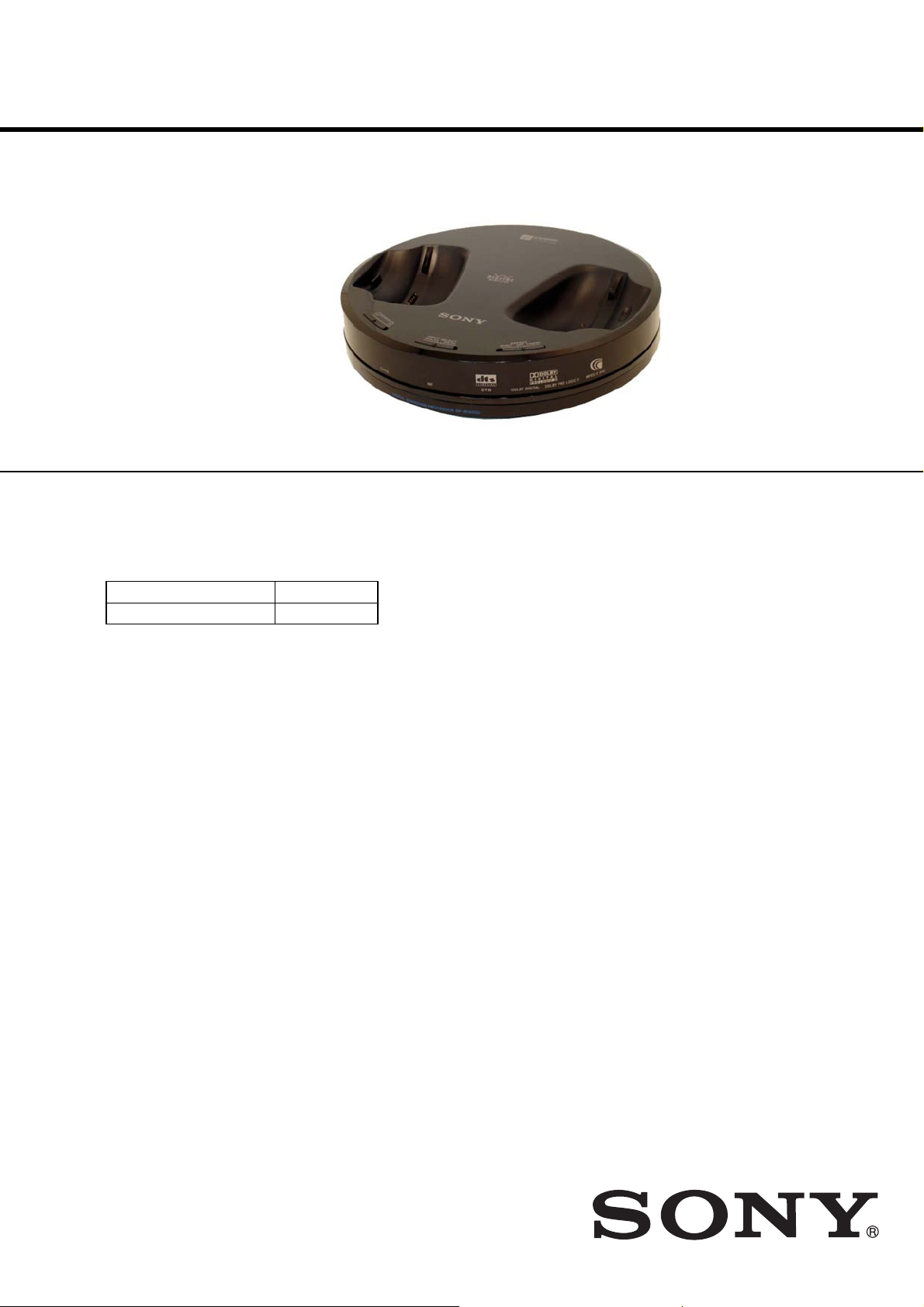
• The DP-RF6000 is the digital surround
processor that comprises the MDR-DS6000.
* The digital surround processor for this system incorporates the Dolby Digital decoder, the Dolby Pro Logic II
decoder, the DTS decoder and the MPEG-2 AAC decoder.
Manufactured under licence from Dolby Laboratories and Digital Theater Systems, Inc.
“Dolby,” “Pro Logic,” the “AAC” logo and the double-D symbol are trademarks of Dolby Laboratories.
“DTS” and “DTS VIRTUAL ” are trademarks of Digital Theater Systems, Inc.
• MDR-DS6000 consists of the following models respectively.
Cordless stereo headphone MDR-RF6000
Digital surround processor DP-RF6000
SPECIFICATIONS
Decoder functions Dolby Digital
Dolby Pro Logic II
DTS
MPEG-2 AAC
Virtual surround function OFF
CINEMA
MUSIC
Compression function OFF
ON
Modulation System DSSS
Carrier wave frequency 2.412 ~ 2.462 GHz (US, Canadian)
2.412 ~ 2.472 GHz (AEP)
2.417 ~ 2.467 GHz (Korea)
Transmission distance Approx. 30 m (100 ft) of longest
Frequency response 12 – 22,000 Hz
(digital input, sampling frequency 48 kHz)
Distortion rate 1% or less (1 kHz)
Audio inputs Optical digital input
(rectangular-type) × 1
Analog input (pin jack left/right) × 1
Audio output Optical digital output
(rectangular-type) × 1
Power requirements DC 9 V
(from the supplied AC power adaptor)
Dimensions Approx. 182 × 38 × 182 mm
(7 1/4 × 1 1/2 × 7 1/4 in) (w/h/d)
Mass Approx. 345 g
(12.17 oz)
US Model
AEP Model
9-887-076-01
2006B02-1
© 2006.02
Design and specifications are subject to change without notice.
DIGITAL SURROUND PROCESSOR
Sony Corporation
Personal Audio Division
Published by Sony Techno Create Corporation
Page 2

DP-RF6000
Notes on chip component replacement
• Never reuse a disconnected chip component.
• Notice that the minus side of a tantalum capacitor may be
damaged by heat.
Unleaded solder
Boards requiring use of unleaded solder are printed with the lead
free mark (LF) indicating the solder contains no lead.
(Caution: Some printed circuit boards may not come printed with
the lead free mark due to their particular size.)
: LEAD FREE MARK
Unleaded solder has the following characteristics.
•Unleaded solder melts at a temperature about 40°C higher than
ordinary solder.
Ordinary soldering irons can be used but the iron tip has to be
applied to the solder joint for a slightly longer time.
Soldering irons using a temperature regulator should be set to
about 350°C.
Caution: The printed pattern (copper foil) may peel away if
the heated tip is applied for too long, so be careful!
• Strong viscosity
Unleaded solder is more viscous (sticky, less prone to flow)
than ordinary solder so use caution not to let solder bridges
occur such as on IC pins, etc.
• Usable with ordinary solder
It is best to use only unleaded solder but unleaded solder may
also be added to ordinary solder.
TABLE OF CONTENTS
Specifications ............................................................................ 1
1. GENERAL ................................................................... 3
2. DIAGRAMS ................................................................. 4
2-1. Block Diagrams ............................................................... 5
2-2. Printed Wiring Board – TX Board Section (Side A) – .... 6
2-3. Printed Wiring Board – TX Board Section (Side B) – .... 7
2-4. Printed Wiring Board
– FUNCTION, CHARGE Boards Section – ................... 8
2-5. Schematic Diagram – TX Board Section (1/4) – ............ 9
2-6. Schematic Diagram – TX Board Section (2/4) – ............ 10
2-7. Schematic Diagram – TX Board Section (3/4) – ............ 11
2-8. Schematic Diagram – TX Board Section (3/4) – ............ 12
2-9. Schematic Diagram
– TX (4/4), FUNCTION, CHARGE Boards Section – ... 13
2-10. IC Pin Function Descriptions .......................................... 15
3. EXPLODED VIEWS
3-1. Processor Section ............................................................ 20
4. ELECTRICAL PARTS LIST .................................. 21
• Repaier DP-RF6000 with MDR-RF6000.
2
Page 3
DP-RF6000
LOCATING THE CONTROLS
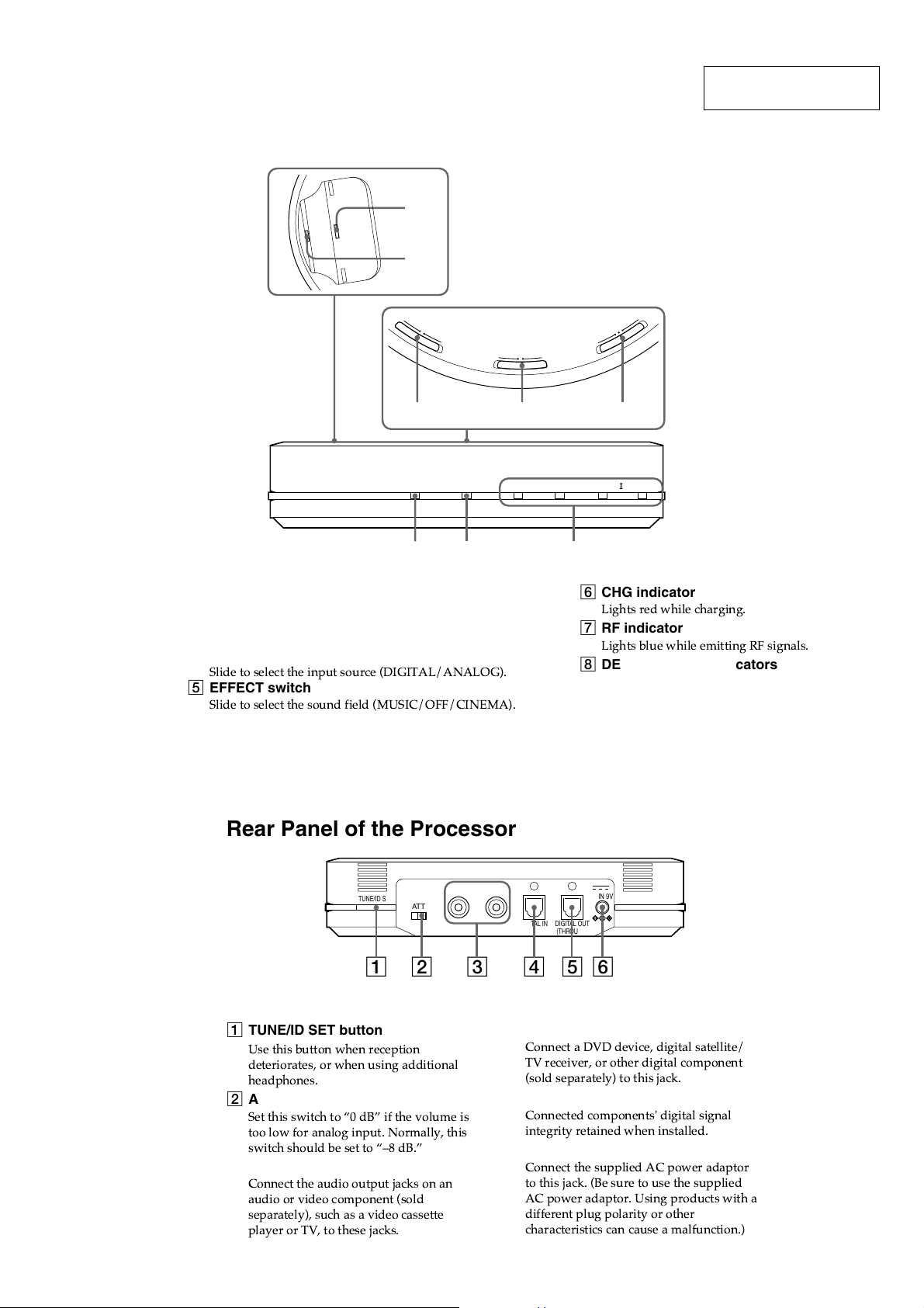
Front Panel of the Processor
SECTION 1
GENERAL
1
2
C
O
O
M
F
P
F
R
E
S
S
I
O
N
O
N
3
CHG RF DTS
I
N
P
A
N
A
A
M
T
E
C
N
E
I
F
C
F
E
F
F
O
C
I
S
U
T
C
U
E
L
T
E
S
L
A
T
I
L
G
O
I
G
D
M
45
DOLBY DIGITAL DOLBY PRO LOGIC MPEG-2 AAC
This section is extracted
from instruction manual.
6
7 8
1 Contact pin
2 Charging lever
3 COMPRESSION switch
4 INPUT SELECT switch
5 EFFECT switch
Rear Panel of the Processor
TUNE/ID SET
0dB -8dB
12 3 456
R
ATT
LLINE IN
DIGITAL IN DIGITAL OUT
6 CHG indicator
! " #!!
7 RF indicator
! $ " %! & !#
8 DECODE MODE indicators
DC IN 9V
(THROUGH)
1 TUNE/ID SET button
Use this button when reception
deteriorates, or when using additional
headphones.
2 ATT (attenuator) switch
Set this switch to Ò0 dBÓ if the volume is
too low for analog input. Normally, this
switch should be set to ÒÐ8 dB.Ó
3 LINE IN jacks
Connect the audio output jacks on an
audio or video component (sold
separately), such as a video cassette
player or TV, to these jacks.
4 DIGITAL IN jack
Connect a DVD device, digital satellite/
TV receiver, or other digital component
(sold separately) to this jack.
5 DIGITAL OUT jack
Connected components' digital signal
integrity retained when installed.
6 DC IN 9V jack
Connect the supplied AC power adaptor
to this jack. (Be sure to use the supplied
AC power adaptor. Using products with a
different plug polarity or other
characteristics can cause a malfunction.)
3
Page 4
DP-RF6000
SECTION 2
DIAGRAMS
NOTE FOR PRINTED WIRING BOARDS AND SCHEMATIC DIAGRAMS.
For schematic diagrams.
Note:
• All capacitors are in µF unless otherwise noted. (p: pF) 50 WV or
less are not indicated except for electrolytics and tantalums.
• All resistors are in Ω and 1/4 W or less unless otherwise specified.
•%: indicates tolerance.
• f : internal component.
• C : panel designation.
• A : B+ Line.
• Power voltage is dc 9 V and fed with regulated dc power supply
from external power voltage jack.
•Voltages and waveforms are dc with respect to ground under nosignal conditions.
•Voltages are taken with a VOM (Input impedance 10 MΩ).
Voltage variations may be noted due to normal production tolerances.
•Waveforms are taken with a oscilloscope.
Voltage variations may be noted due to normal production tolerances.
• Circled numbers refer to waveforms.
• Signal path.
F : ANALOG
J : DIGITAL
For printed wiring boards.
Note:
• X : parts extracted from the component side.
• f : internal component.
• : Pattern from the side which enables seeing.
Caution:
Pattern face side: Parts on the pattern face side seen from
(Side B) the pattern face are indicated.
Parts face side: Parts on the parts face side seen from
(Side A) the parts face are indicated.
• Indication of transistor.
C
Q
B
E
These are omitted.
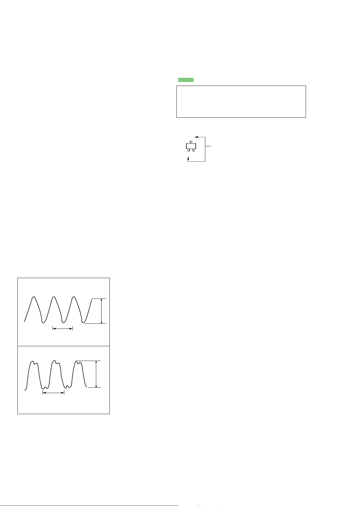
• Waveforms
– TX BOARD –
IC201
1
0.5V/DIV, 0.1 µsec/DIV
2
1V/DIV, 20 nsec/DIV
i;
203 ns
IC4001 A
2
83.2 ns
XO
1.5Vp-p
3.8Vp-p
4
Page 5
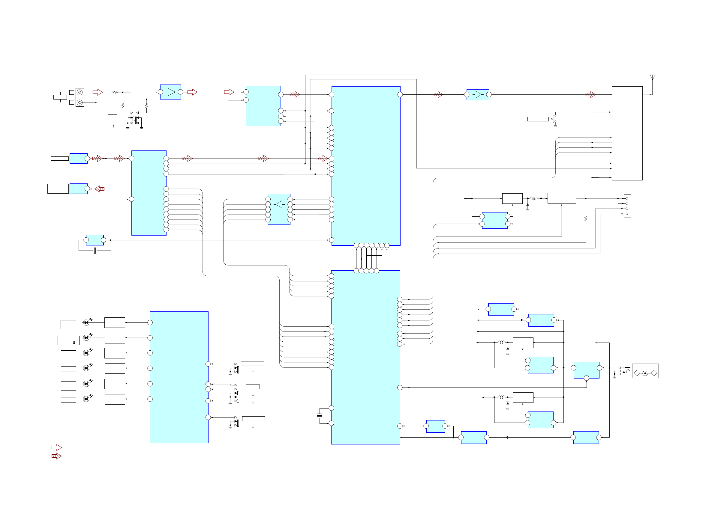
2-1. BLOCK DIAGRAM
DP-RF6000
J051
L
LINE IN
DIGITAL IN
DIGITAL OUT
(THROUGH)
DOLBY PRO
R
IC001
OPTICAL
RECEIVER
IC004
OPTICAL
TRANSMITTER
D522
DOLBY
DIGITAL
D523
LOGIC
D524
DTS
D521
CHG
D525
MPEG-2
AAC
D526
RF
VOUT
VIN
1
3
IC4001
CLOCK OSC
2
OUT
IN
X4000
12.288MHz
R-CH
4
S051
ATT
-8dB
0dB
Q202
LED DRIVER
Q203
LED DRIVER
Q204
LED DRIVER
Q205
LED DRIVER
Q206
LED DRIVER
Q207
LED DRIVER
• R-ch is omitted due to same as L-ch.
• SIGNAL PATH
: ANALOG
: DIGITAL
ANT4000
ANT
3
CHARGE
4
TERMINAL
5
(TO MDR-RF6000)
2
J301
DC IN 9V
+-
IC052
LINE AMP
5 7
R-CH
IC002
DIR
22
DATAO
RXIN
12
XIN
24
100
99
98
97
96
95
BCK
LRCK
CKOUT
ERROR
PD
DO
E/INT
AUDIO
UGPI
P20
P17
P16
P21
P15
P14
CE
CL
DI
20
21
19
2
3
5
6
7
8
9
10
11
DIR_ERR
DIR_XRST
DIR_XCS
DIR_EMP
DIR_NAUD
DIR_XST
IC201(2/2)
SYSTEM
CONTROLLER
SCK2
SDO2
SDI2
P34
P35
P37
P36
P33
R-CH
DIRDATA
BCK
LRCK
MCKDIR
DSP_NOSG
DEC_INTREQ
SDI1
DSP_XINTREQ
DSP_HINBSY
MCK
12
13
15
14
11
AUDIO A/D
CONVERTER
8 LIN
7RIN
S502
INPUT SELECT
DIGITAL
ANALOG
S501
EFFECT
MUSIC
OFF
CINEMA
S503
COMPRSSION
ON
OFF
IC003
SDATO
BCK
ADCLRC
MCLK
IC1202(1/2)
LEVEL SHIFT
18
16
14
12
9
2
3
12
13
DIR_ERR
DIR_XRST
DIR_XCS
SCK2
SDO2
SDI2
DIR_EMP
DIR_NAUD
DIR_XST
2
4
6
8
11
DSP_NOSG
DEC_INTREQ
SDI1
DSP_XINTREQ
DSP_HINBSY
x201
131
FSDATAN1
111
FSCLKN2
134
FSCLKN1,STCCLK2
119
FLRCLKN1
117
FLRCLKN2
98
SCLK1
87
LRCLK1
FSDATAN2
118
SCLK0
104
LRCLK0
108
MCLK
99
GPIO15
31
XFINTREQ
16
FHS2,FSCDOUT
7
XINTREQ
3
HINBSY
141
CLKIN
127
P73
28
P74
29
16
SIN2
30
P75
31
P76
P56
74
P57
76
P54
73
SCK1
58
SDO1
57
56
SIN1
72
P54
PA3
67
PA2
66
x0
80
x1
81
IC1201
DECODER,DSP
XRESET
SCCLK
144
142 136 135
P62
SCK2
IC201(1/2)
SYSTEM
CONTROLLER
SCDIN
SOT2
SCCS
15 4
3217 3938 18
P63
AFCS
P77
FSCDIN
FSCCLK
6
XRST
DTO
P13
P12
P10
P11
P07
P02
AN1
AN0
P01
P00
IC1202(2/2)
LEVEL SHIFT
110
UNREG_9V
5V ON
CHG_ON
VBATT2
BATT_TEMP
BATT_DET
BATT_TEMP
MAPOW
INRST
ID STATE
CH_SYNC
TXON
5V ON
CHG_ON
VBATT2
BATT_DET
IC202
RESET
1
INOUT
2
94
93
91
92
90
85
37
36
84
83
75
VCC
17
+5V REGULATOR
3
4
REG3.3V
REG_5V
REG_9V
REG2.5V
VDD3.8V
IC4006
+3.3V REGULATOR
5
VIN
VOUT
3
SWITCHING
IC4002
ID4000
VINCEEXT
VOUT
IC304
+3.3V REGULATOR
3
D302
D4000
D205
1
Q4001
1
7
INOUT
D4001
2
Q301
SWITCHING
Q4000
SWITCHING
S504
TUNE/ID SET
IC302
+5V REGULATOR
1
+2.5V REGULATOR
1
5
+3.8V REGULATOR
1
5
EXT
VOUT
IC4004
EXT
VOUT
INOUT
IC305
VDD
VDD
INRST
ID STATE
CH_SYNC
TXON
Q4002,4003
CHARGE SWITCH
3
2
MAPOW
2
CH/ID SYNC_BUTTON
VDD3.8V
UNREG_9V
+9V REGULATOR
2
+5V REGULATOR
1
DSPOUT
ID STATE
RXON (CH_SYNC)
IC301
INOUT
1
CE
4
IC303
INOUT
3
INRST
TXON
BCK
LRCK
VDD3.8
BATT_TEMP
BATT_DET
BATT2
TX-RF
BLOCK
CN601
DP-RF6000
55
Page 6
DP-RF6000
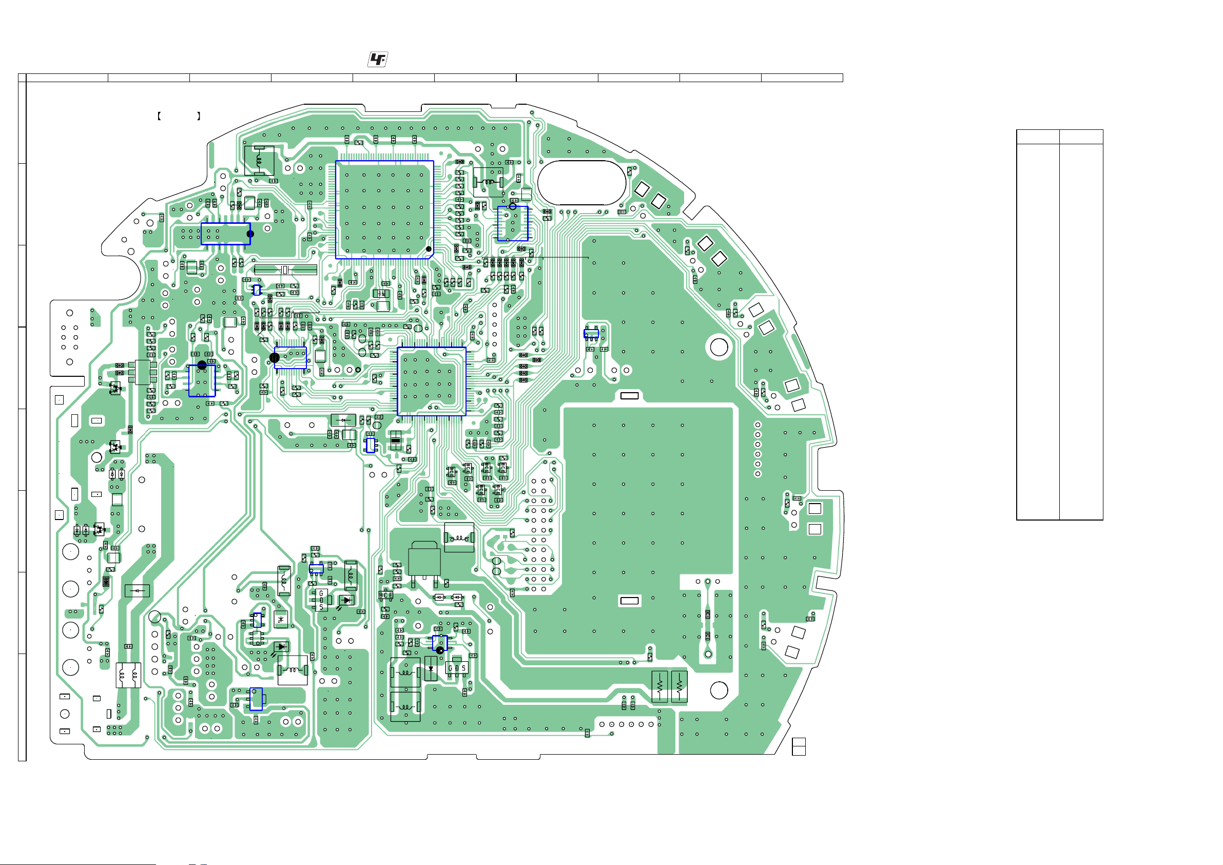
2-2. PRINTED WIRING BOARD – TX BOARD SECTION (SIDE A) –
1
A
2
TX BOARD (SIDE A)
B
C517
L052
R062
R301
R063
C310
C301
C305
C074
C060
C308
R059
C077
1
IC052
4
C
R055
R053
R051
C052
D
E
F
D053
G
L055
L054
D052
D057
D055
054
D
C001
L001
R001
C003
LF301
R002
D051
L062
C014
L002
C303
D056
R052
C051
R054
R056
L053
D301
LF051
1
H
34567
L1204
73
C1222
L051
R068
C072
R057
C068
7
8
C070
R058
C078
C057
8
5
R065
C069
IC003
IC4001
C080
C056
L056
C066
C059
R060
R069
C315
C311
R067
L063
1
14
C4011
C064
R061
IC305
1
3
4
6
1
3
R066
1
3
R024
L008
L005
R013
R009
C002
C316
Q301
IC304
C312
C075
X4000
C4009
5
4
R4002
L4005
R020
24
1
IC002
R010
L303
C318
5
4
3
D302
1
L006
R4009
L301
L007
R4001
C4010
R021
R017
13
12
R004
R005
R4000
C1210
C1208
R4003
R023
R022
C009
C008
C005
R014
5
1
IC4004
Q4000
C4007
C015
C4004
R4008
108
C222
4
C4001
3
R1202
L009
L003
109
L1202
D205
C217
72
C206
C4002
D4000
C1217
C229
SL201
L202
C216
L4001
R1249
C1201
R228
C4000
: Uses unleaded solder.
C1216
C1215
C1214
IC1201
C1205
C1202
C1207
R1214
C1206
SL202
R236
R271
SL203
4
5
IC202
Q4002
R221
R223
R206
C223
C226
3
1
R4020
C4023
R4010
C4021
C4018
C4016
R4007
L4002
L4003
L1201
C224
R222
51
75
C212
X201
R286
R4017
R4006
C1204
R1215
R220
50
76
R4011
C1203
SL204
R273
C210
C228
R289
B
R4019
R4005
IC201
R288
C
Q4003
C4017
D4001
37
144
L1210
R1255
Q207
5
C4015
8
36
R1254
R1245
R1244
R1243
C1211
R1240
R1238
R1236
R1235
R1233
L1207
1
R1252
R1227
C1220
E
D4003
C1209
L1206
R1216
C227
R4015
C4013
L1209
R1217
100
Q206
D4002
R4004
4
IC4002
1
26
Q204
R1219
C207
R269
C225
R4028
L1203
R1228
R1220
C209
25
1
C201
Q202
C220
C4027
Q4001
L1208
R224
R270
C218
L4007
C4014
R1253
C211
C202
C1221
1
10
R210
SL205
SL206
C1218
R229
R276
C205
R275
C204
R274
C203
Q203
C219
C1224
L1213
Q205
C221
R4024
L1205
20
11
C208
L551
C4042
L4004
R4027
IC1202
R1258
R4030
R4031
L552
L553
L554
L555
R1251
L1211
R1256
L1212
R1257
C4032
R1261
L1214
R1259
R1262
IC4006
C4038
5
1
L1215
R1260
8
910
• Semiconductor Location
Ref. No. Location
D051 E-2
D052 D-2
R501
C515
R503
C513
C512
R4033
R504
C514
R517
C511
1-868-111-
R502
C518
R519
C516
31
(31)
4
3
C4033
R4032
R287
R4013
C4039
R4014
C4040
D053 F-1
D054 F-1
D055 F-1
D056 E-2
D057 E-1
D205 E-4
D301 G-2
D302 G-4
D4000 G-4
D4001 H-5
D4002 G-6
D4003 G-6
IC002 D-4
IC003 B-3
IC052 D-3
IC201 D-5
IC202 E-5
IC304 H-4
IC305 G-3
IC1201 B-5
IC1202 B-7
IC4001 C-3
IC4002 G-6
IC4004 F-4
IC4006 D-7
Q202 E-6
Q203 E-6
Q204 F-6
Q205 E-6
Q206 E-6
Q207 E-6
Q301 G-3
Q4000 G-4
Q4001 H-6
Q4002 G-5
Q4003 F-5
DP-RF6000
66
Page 7
DP-RF6000
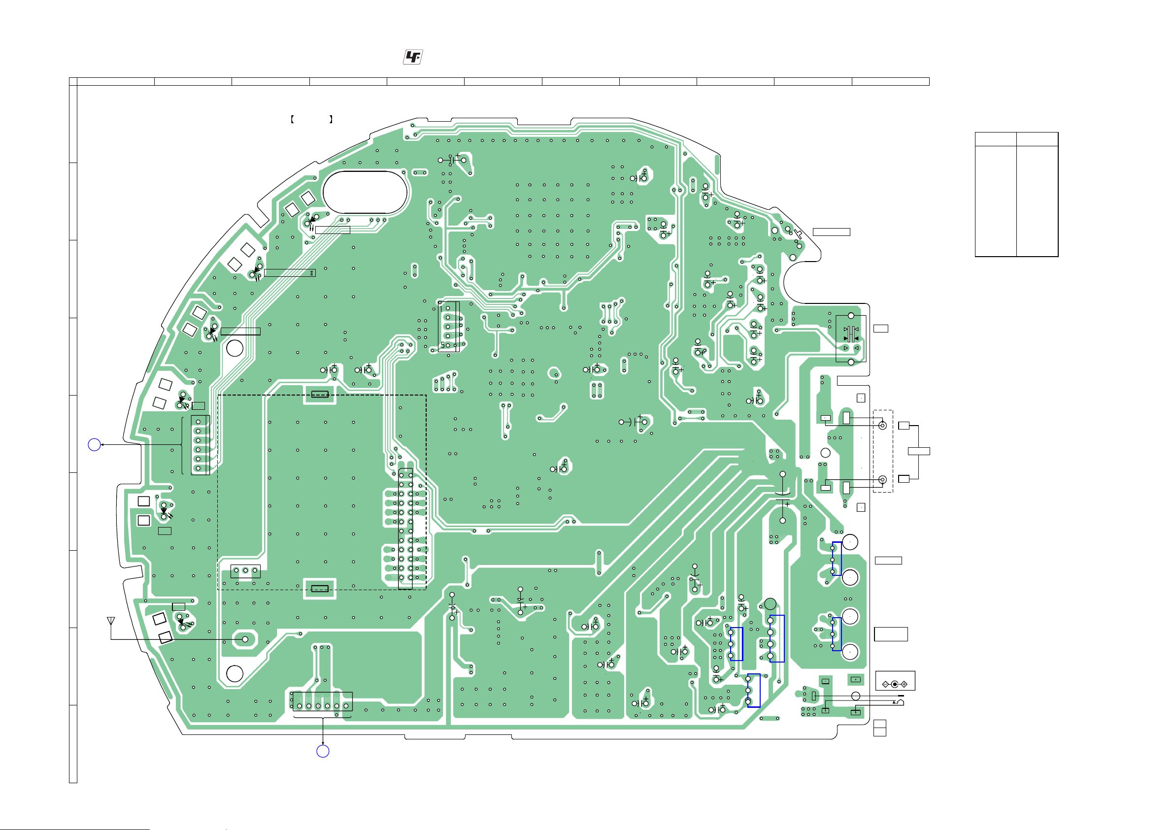
2-3. PRINTED WIRING BOARD – TX BOARD SECTION (SIDE B) –
1
2
A
B
C
D522
DOLBY DIGITAL
D
3 4 5 6 7
TX BOARD (SIDE B)
D525
MPEG-2 AAC
D523
DOLBY PRO LOGIC
C4031
C4034
: Uses unleaded solder.
C1212
CN202
C010
C1213
C073
8
C058
C065
C076
C071
9 10 11
S504
TUNE / ID SET
C055
C067
C063
C062
C053
C054
S051
ATT
0dB
t
-8dB
• Semiconductor Location
Ref. No. Location
D521 G-2
D522 D-2
D523 C-3
D524 E-2
D525 B-4
D526 F-2
IC001 G-10
IC004 H-10
IC301 H-10
IC302 H-9
IC303 H-9
E
F
G
H
A
FUNCTION
BOARD
(Page 8)
ANT4000
D526
RF
D521
CHG
D524
DTS
1
6
CNP201
CNP4002
TX-RF BLOCK
CNP4001
2
1
23
24
C4012
C4020
C213
C4003
C4008
C214
C314
C317
C309
C307
IC303
1
3
C061
C302
IC302
3
C304
IC301
4
1
J051
R
LINE IN
L
3
IC001
1
3
IC004
1
DIGITAL IN
DIGITAL OUT
(THROUGH)
J301
DC IN 9V
DP-RF6000
6
I
1
C313
CN203
CHARGE
BOARD
B
(Page 8)
C306
1
1-868-111-
31
(31)
77
Page 8
DP-RF6000
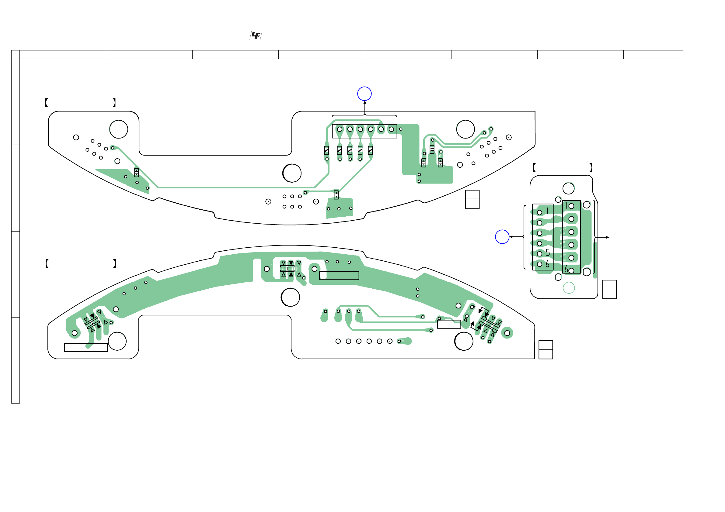
2-4. PRINTED WIRING BOARD – FUNCTION, CHARGE BOARDS SECTION –
2
C555
A
1
FUNCTION BOARD (SIDE A)
B
: Uses unleaded solder.
3 4 5 6 7
TX
A
BOARD
(Page 7)
CN501
6
R555
R551
C554
R553
R552
R554
1
1-868-112-
C551
C553
C552
31
CHRGE BOARD
CNP601
CN601
(31)
8
C
D
FUNCTION BOARD (SIDE B)
t
OFF ON
S503
COMPRESSION
ANALOG DIGITAL
t
S502
INPUT SELECT
S501
EFFECT
BOARD
(Page 7)
MUSIC
TX
B
t
OFF CINEMA
1-868-112-
t
31
(31)
1-868-110-
CHARGE
TERMINAL
(TO MDR-RF6000)
31
(31)
DP-RF6000
88
Page 9

DP-RF6000
2-5. SCHEMATIC DIAGRAM – TX BOARD SECTION (1/4) –
D051
D052
L053
0uH
L054
0uH
L055
0uH
D054
1SS355TE-17
MA3130WA-TX
J051
MA3130WA-TX
MA3130WA-TX
D053
1SS355TE-17
• See page 13, 14 for IC Block Diagrams.
C051
R052
100p
680k
D055
LF051
COM MODE
R053
47k
R051
680k
D056
1SS355TE-17
R054
C052
100p
47k
C053
10
16V
R055
9.1k
R056
9.1k
1SS355TE-17
D057
C054
C078
100p
S051
10
16V
R059
22k
R057
47k
uPC4552G2
C055
100
6.3V
IC052
R058
22k
L062
10uH
C077
100p
C056
0.1
R069
C061
10
16V
VCC
R062
22k
C065
100
16V
C062
C064
0.1
22
16V
R067
1k
IC003
WM8738GED/R
C063
22
16V
R065
1k
C066
0.1
C067
10
16V
C069
C068
0.1
0.1
R063
22k
C060
180p
VEE
C059
180p
R061
22k
R060
22k
C058
10
16V
L056
15uH
C057
0.1
1k
LRCK
C076
10
16V
BCK
C070
0.1
MCKDIR
R066
100
L063
0uH
R068
470
ADDATA
C071
16V
L052
C072
C074
15uH
0.1
C073
C075
10
0.1
16V
L051
15uH
0.1
10
J301
DC IN 9V
LF301
D301
RB051L-40TE25
C303
C080
0.001
Q4000
XP162A11C0PR
SWITCHING
C4007
C4008
C318
6.3V
100
16V
L303
47uH
C317
2200
6.3V
C316
33
0.1
Q301
RTQ035P02TR
IC301
PQ09RD11J00H
+9V REG
C301
0.1
0.1
C304
10000
25V
R301
_3.9V
MAPOW
UNSW
10k
C302
100
16V
REG_3.3V
IC302
KIA78S05P-TP
+5V REG
C305
C306
0.1
100
6.3V
C311
0.1
REG_3.3V
C307
100
6.3V
REG_2.5V
KIA78S05P-TP
+5V REG
C308
0.1
IC303
C309
100
16V
VDD3.8V
UNREG_9V
C310
0.1
IC304
XC6206P332PR
+3.3V REG
C312
0.1
C313
6.3V
100
SWITCHING
D302
RB161M-20FTR
C314
100
16V
C315
0.1
L301
22uH
IC305
XC6365A253MR
+2.5V REG
0.1
R4000
10
C4002
0.1
D4000
RB160M-30TR
XC6365A253MR
+3.8V REG
IC4004
L4001
47uH
R4008
C4001
0.1
330k
C4004
R4009
120k
C4000
0.1
47p
C4003
100
16V
S 1
GND
BU
DP-RF6000
TX
BOARD
(2/4)
(Page 10)
TX
BOARD
(3/4)
(Page 11)
TX
BOARD
(4/4)
(Page 12)
TX
BOARD
(3/4)
TX
BOARD
(4/4)
(Page 12)
TX
BOARD
(2/4)
(Page 10)
(Page 11)
99
Page 10

DP-RF6000
2-6. SCHEMATIC DIAGRAM – TX BOARD SECTION (2/4) –
OPTICAL
L003
15uH
C015
0.1
DSP_NOSG_L
DSPOUT
DEC_XINTREQ_L
SDI1_L
DSP_XINTREQ_L
DSP_HINBSY
OPTICAL RECEIVER
T
S
X
_
IR
D
L009
0uH
R1256
C001
0.47
L001
0uH
T
S
R
X
_
IR
D
C010
R
R
E
_
IR
D
47
10V
L002
10uH
R010
R014
R013
C4011
SN74LVC244APWR
C014
0.1
10k
10k
R009
C002
10k
0.1
C1224
0.1
IC1202
LEVEL SHIFT
10k
0.01
LC89052T-TLM-E
C003
0.47
R002
R001
100
100
2
2
P
D
U
M
A
E
_
N
_
IR
IR
D
D
8
0
0
C
6
0
.0
0
R017
150
C009
0.047
R4027
330
S
I2
K
O
C
D
C
X
D
S
S
_
S
IR
D
k
k
1
1
4
5
0
0
0
0
R
R
8
C005
0.1
0uH
L4004
330
L1211
0uH
BOARD
(1/4)
(Page 9)
(Page 11)
TX
BOARD
(1/4)
(Page 9)
TX
BOARD
(3/4)
(Page 11)
TX
BOARD
(4/4)
(Page 12)
TX
TX
BOARD
(3/4)
IC001
TORX147L
IC004
TOTX147L
(RED)
TRANSMITTER
MAPOW
UNSW_3.9V
REG_3.3V
REG_3.3V
GND
BUS 1
• See page 14 for IC Block Diagrams. • See page 4 for Waveforms. • See page 15 for IC Pin Function Discription.
IC002
L1205
10uH
L1213
L1212
C4010
C4009
L1214
27p
R4001
27p
L1215
0uH
0uH
X4000
12.288MHz
1M
L005
L006
L007
L008
1SR154-400TE25
C222
0.1
0uH
R1261
0uH
0uH
0uH
0uH
0uH
D205
0
R1257
SN74AHC1GU04DCKR
R020
R021
R022
R023
R024
C214
C217
1000
0.1
6.3V
R1259
R1258
330
330
R4002
IC4001
CLOCK OSC
100
330
330
470
330
L202
15uH
C1218
0.1
R1260
R1262
330
T
P
S
R
S
C
R
M
R
X
E
E
_
_
X
_
IR
IR
IR
D
D
R206
1k
SL203
0.1
C212
DIR_XRST
X201
5MHz
R273
2.2k
330
L4005
0uH
R4003
100
MCK
DIRDATA
LRCK
BCK
MCKDIR
C216
C213
100
0.1
6.3V
330
0
DSP_NOSG
DSPOUT_L
DEC_XINTREQ
DSP_XINTREQ
DSP_HINBSY_L
SDI1
C210
BATT_DET
CHG_ON
R286
10k
0.1
5V ON
CH_SYNC
TXON
ID STATE
INRST
RF_LED
LED_AAC
LED_DTS
LED_PL2
LED_DD
CHG_LED
R271
C226
0.033
4.7k
T
S
R
X
NC
CT
IC202
BD5228G
RESET
GND
VDD
VOUT
D
T
D
S
U
X
A
_
N
_
IR
D
IR
D
IC201
MB90488BPFV
-G-150E1
SYSTEM CONTROLLER
H
H
H
u
uH
u
u
0
0
0
0
5
3
4
2
5
5
5
5
55
5
L
L
L5
L
T
P
C
M
U
M
F_
F_
P
O
F
F
E
E
IN
C
_
_
_
_
W
W
W
W
S
S
S
S
uH
0
1
55
L
FF
O
F_
F
E
_
W
S
T
C
U
N
O
R274
V
S
IN
S
E
V
V
C
C4031
100
16V
R220
10k
R275
10k
10k
R276
C4033
4
2
2
C
4
0
2
1
.0
0
L
S
R224
10k
10k
C4034
0.1
100
16V
R289
C228
1
1M
R288
R221
10k
SL201
R222
10k
9
2
2
C
1
.0
0
k
10
8
2
2
R
R229
10k
1M
R223
10k
2
0
2
3
22
C
L
S
1
.0
0
C207
0.001
C208
0.001
0.1
C201
0.1
C202
0.1
C203
0.1
C204
0.1
C205
BATT_TEMP
DSP_XCS
DSP_XRST
VBATT2
DEC_XCS
DSP_HINBSY
DSP_XINTREQ
DEC_XINTREQ
DSP_NOSG
R287
22k
C206
0.1
C209
0.1
IC4006
XC6219B332MR
R269
10k
+3.3V REG
C4032
0.1
R270
10k
2
2
I2
K
O
D
C
D
S
S
S
R236
10k
1
1
O
I1
K
C
D
D
S
S
S
C211
0.1
DP-RF6000
1010
Page 11

DP-RF6000
2-7. SCHEMATIC DIAGRAM – TX BOARD SECTION (3/4) –
T
S
R
X
_
P
S
D
R1215
10k
C1209
R1219
3.3k
DSP_XINTREQ_L
SDO1
SCK1
SDI1_L
R1252
C1211
0.1
H
u
0
330
R1251
L1206
L1207
330
H
u
0
R1227
0.1
10k
R1217
3.3k
R1220
3.3k
R1228
3.3k
C1220
0.1
R1216
3.3k
• See page 17 for IC Pin Function Discription.
L
1
_
K
Y
C
S
S
B
IN
H
_
P
S
D
R1255
330
L1210
0uH
1
S
O
C
X
D
_
S
P
S
D
A
K
T
C
A
B
D
D
A
C1203
K
C
M
C1204
0.1
0.1
C1205
C1201
C1206
0.0012
68p
R1214
3k
4.7
L1201
C1207
2.2
10V
15uH
A
K
K
T
C
C
A
R
R
D
L
L
IR
D
C1202
0.1
L
K
_
C
T
B
U
O
P
S
D
R1202
1k
L1202
10uH
K
K
IR
C
C
D
B
R
K
L
C
M
BUS 1
TX
BOARD
(1/4)
(Page 9)
TX
GND
BOARD
(2/4)
(Page 10)
TX
BOARD
(4/4)
(Page 12)
R1236
10k
C1213
100
4V
DEC_XCS
DEC_XINTREQ_L
DSP_NOSG_L
R1253
R1235
3.3k
L1208
330
R1254
R1233
3.3k
R1238
3.3k
0uH
330
L1209
0uH
R1240
3.3k
R1243
R1244
R1245
3.3k
IC1201
CS494003-CQZ
DECODER,DSP
3.3k
3.3k
R1249
C1214
10k
C1215
0.1
0.1
C1216
0.1
C1217
0.1
L1204
10uH
C1222
0.1
C1208
C1212
C1210
L1203
10uH
C1221
0.1
470
6.3V
0.1
REG_2.5V
REG_3.3V
REG_3.3V
0.1
TX
BOARD
(1/4)
(Page 9)
TX
BOARD
(2/4)
(Page 10)
DP-RF6000
1111
Page 12

DP-RF6000
2-8. SCHEMATIC DIAGRAM – TX (4/4), FUNCTION, CHARGE BOARDS SECTION –
CN501
6P
R4007
680k
C4020
470
0.1
10V
R4020
R4010
R4028
47k
22k
1M
TX
BOARD
(1/4)
(Page 9)
VDD3.8V
UNREG_9V
Q4001
XP162A11C0PR
SWITCHING
S501
C552
0.001
C551
C553
0.001
S503
0.001
S502
D4001
RB051L-40TE25
IC4002
XC9201D09AKR
+5V REG
R552
R551
R553
C555
0.001
R555
1k
1k
1k
1k
C554
0.001
R4006
S
S
V
T
X
E
R554
1k
L4003
47uH
L4002
47uH
C4017
470p
150k
T
U
O
V
N
E
IS
C4016
C4015
33p
220p
R4005
10k
C4018
K
IN
L
A
C
/G
C
C
S
/S
E
IN
C
V
D4002
1SS355TE-17
D4003
1SS355TE-17
R4011
390
Q4002
2SC2712L-TE85L
CHARGE
SWITCH
CNP201
6P
C4039
0.1
R4013
R4017
100k
1.5
1W
Q4003
2SB1412-TLQ
CHARGE
SWITCH
C4023
0.1
R4019
120k
• See page 13 for IC Block Diagrams.
R4033
R4032
0
0
SW_COMP
SW_INPUT
R4014
1.5
1W
R4015
10k
SW_EFF_M
SW_EFF_C
SW_EFF_OFF
CHG_ON
VBATT2
SYNC_BUTT
TXON
BCK
LRCK
DSPOUT
CH_SYNC
INRST
ID STATE
SYNC_BUTT
L4007
47uH
C517
ANT4000
3P
CNP4002
100
R4030
R4031
100
1k
R4024
C4042
0.001
SL205
SL206
S504
0.1
CNP4001
25P
TX
BOARD
(1/4)
(Page 9)
TX
BOARD
(2/4)
(Page 10)
TX
BOARD
(3/4)
(Page 11)
BUS 1
C4021
R4004
SLR342VC3F
C513
0.001
Q202-207
LED DRIVER
0.001
D524
C220
C4027
R502
680
2
L
P
_
D
E
L
0.22
DTS
Q204
DTC123YUA
C514
0.001
C4013
0.1
C4012
220
16V
DOLBY
0.001
C511
D522
SLR342VC3F
D
E
L
_
G
H
C
C218
0.001
R210
4.7k
R504
680
DIGITAL
Q202
DTC123YUA
CHG
R517
680
D521
SLR342VC3F
C516
0.001
C221
GND
0.001
Q205
DTC123YUA
C512
0.001
D523
SLR342VC3F
C219
0.001
C4014
DOLBY PRO
R503
680
D
D
_
D
E
L
1
16V
LOGIC
Q203
DTC123YUA
10k
D525
SLR342VC3F
S
T
D
_
D
E
L
C225
0.001
R501
680
0.1
MPEG-2
AAC
Q206
DTC123YUA
SLR343BBT3FXG
C515
0.001
5V ON
RF
R519
3.3k
D526
C518
0.001
C
A
A
_
D
E
L
C227
0.001
DTC123YUA
Q207
D
E
L
F_
R
BATT_DET
BATT_TEMP
C4040
0.1
C4038
0.1
CN203
6P
CN601
6P
CNP601
6P
CHARGE
TERMINAL
(TO MDR-RF6000)
DP-RF6000
1212
Page 13

• IC BLOCK DIAGRAMS
IC305 XC6365A253MR
5
DP-RF6000
V OUT
1
EXT/
VDD
2
3
GND
IC4002 XC9201D09AKR
1
EXT
BUFFER,
DRIVER
PWM
COMPARATOR
RAMP WAVE
GENERATOR
OSC
EXT TIMMING
CONTROL
LOGIC
COMPENSATION
+
-
CONTROLLER
PHASE
PWM/PFM
CURRENT
LIMIT
PROTECTION
ERROR AMP.
+
-
VREF WITH
SOFT START,
CE
4
CE
8
V SS
7
V OUT
R1
ISEN
V IN
CE/SS
2
3
4
LIMITTER COMP.
INTERNAL
VOLTAGE
REGULATOR
CHIP ENABLE,
SOFT START UP,
U.V.L.O.
PWM
2.0V
TO INTERNAL
CIRCUIT
CE,UVLO
TO INTERNAL
CIRCUIT
MIX
SAMPLING
VREF GENERATOR
LERR
0.9V
VERR
RAMP WAVE,
INTERNAL CLK
GENERATOR
R2
6
CC/GAIN
5
CLK
13
Page 14

DP-RF6000
IC4004 XC6365B103MR
EXT/
VDD
GND
IC4006 XC6219B332MR
VSS
PWM
COMPENSATION
COMPARATOR
+
BUFFER,
1
PHASE
DRIVER
2
3
1VIN
2
RAMP WAVE
GENERATOR
VOLTAGE
REFERENCE
OSC
-
PWM/PFM
CONTROLLER
-
+
ERROR AMP.
CURRENT
LIMIT
+
-
VREF WITH
SOFT START,
CE
R1
5
FB
4
CE
5
VOUT
R2
3
CE
ON/OFF
CONTROL
EACH
CIRCUIT
4NC
14
Page 15

2-9. IC Pin Function Descriptions
• IC201 MB90488BPFV-G-150E1 SYSTEM CONTROL (TX BOPARD)
Pin No. Pin Name I/O Description
1 to 8 P22 to P27, P30, P31 — Not used (Open)
9 VSS — Ground
10 P32 — Not used (Open)
11 P33 I COMPRESSION switch signal input (L : ON,H:OFF)
12 P34 I INPUT SELECT switch signal input (L : DIGITAL,H:ANALOG)
13 P35 I EFFECT switch signal input (L : MUSIC)
14 P36 I EFFECT switch signal input (L : CINEMA)
15 P37 I EFFECT switch signal input (L : EFFECT OFF)
16 SIN2 I Serial data input from CS494003-CQZ
17 SOT2 O Serial data output to CS494003-CQZ
18 SCK2 O Serial clock output to CS494003-CQZ
19, 20 P43, P44 — Not used (Open)
21 VCC5 — Power supply (+3.3V)
22 to 24 P45 to P47 — Not used (Open)
25 SIN0 I Serial data input for flash (Open)
26 SOT0 O Serial data output for flash (Open)
27 SCK0 O Serial clock signal output for flash (Open)
28 P73 I DSP_NOSG signal input from CS494003-CQZ
29 P74 I DEC Interrupt request signal input from CS494003-CQZ
30 P75 I DSP Interrupt request signal input from CS494003-CQZ
31 P76 I DSP HINBSY signal input from CS494003-CQZ
32 P77 O DEC chip select signal output to CS494003-CQZ
33 AVCC — Power supply terminal (+3.3V)
34 AVRH I A/D converter external reference power supply input
35 AVSS — Ground
36 AN0 I Battery temperature detection signal input
37 AN1 I Battery voltage level detection signal input
38 P62 O DSP reset signal output to CS494003-CQZ
39 P63 O DSP Chip select signal output to CS494003-CQZ
40 VSS — Ground
41 to 44 P64 to P67 — Not used (Open)
45 P80 — Not used(Pull up)
46 P81 — Not Used(Pull down)
47 MD0 I Mode setting input terminal
48 MD1 I Mode setting input terminal
49 MD2 I Mode setting input terminal
50 to 55 P82 to P87 — Not used (Open)
56 SIN1 I Serial data input from LC89052T-TLM-E
57 SOT1 O Serial data output to LC89052T-TLM-E
58 SCK1 O Serial clock output to LC89052T-TLM-E
59 P93 — Not used (Pull down)
60 to 65 P94 to P97, PA0, PA1 — Not used (Open)
66 PA2 I Function setting signal input from LC89052T-TLM-E
67 PA3 I PCM detection signal input from LC89052T-TLM-E
68 to 71 P50 to P53 — Not used (Open)
72 p54 I Emphasis signal input from LC89052T-TLM-E
73 P55 O Chip select signal output to LC89052T-TLM-E
74 P56 I Error signal input from LC89052T-TLM-E
DP-RF6000
15
Page 16

DP-RF6000
Pin No. Pin Name I/O Description
75 XRST I System reset signal input
76 P57 O Reset signal output to LC89052T-TLM-E
77 X1A — Not used (Open)
78 X0A — Not used (Connect to Ground)
79 VSS — Ground
80 X0 O Clock output (4MHz)
81 X1 I Clock input (4MHz)
82 VCC3 — Power supply (+3.3V)
83 P00 O REG+9V Main Power supply ON/OFF signal output
84 P01 I Battery detection signal input
85 P02 O Battery charge ON/OFF signal output
86 to 89 P03 to P06 — Not used (Open)
90 P07 O 5V DC-DC converter ON/OFF signal output
91 P10 I Channel SYNC signal input from TX-RF block
92 P11 O RF output enable signal output to TX-RF block
93 P12 I ID state signal input from TX-RF block
94 P13 O IA8 Reset signal output to TX-RF block
95 P14 O RF LED drive signal output
96 P15 O AAC LED drive signal output
97 P16 O DTS LED drive signal output
98 P17 O DOLBY PRO LOGIC II LED drive signal output
99 P20 O DOLBY DIGITAL LED drive signal output
100 P21 O CHARGE LED drive signal output
16
Page 17

• IC1201 CS494003-CQZ DECODER/DSP (TX BOARD)
Pin No. Pin Name I/O Description
1 UHS0 I Mode select signal input
2 UHS1 I Mode select signal input
3 XINTREQ O DSP Interrupt request signal output to MB90488BPFV-G-150E1
4 FSCDIN I Serial data input from MB90488BPFV-G-150E1
5 GPIO20 — Not used (Open)
6 FSCCLK I Serial clock signal input from MB90488BPFV-G-150E1
7 FHS2, FSCDOUT O Serial data output to MB90488BPFV-G-150E1
8 GPIO21 — Not used (Open)
9 FDAT7 — Not used (Open)
10 VDD6 — Power supply (+2.5V)
11 VSS6 — Ground
12 FHS0 I Mode select signal (Pull up)
13 FHS1 I Mode select signal (Pull down)
14 FDAT6 — Not used (Open)
15 XFCS I DEC Chip select signal input from MB90488BPFV-G-150E1
16 XFINTREQ O DEC Interrupt request signal output to MB90488BPFV-G-150E1
17 FDBCK — Not used (Pull up)
18 FDAT5 — Not used (Open)
19 FDAT4 — Not used (Open)
20 VDD7 — Power supply (+2.5V)
21 VSS7 — Ground
22 FDAT3 — Not used (Open)
23 FDBDA I Not used (Pull up)
24 FDAT2 — Not used (Open)
25 DBDA I Not used (Pull up)
26 DBCK I Not used (Pull up)
27 FDAT1 — Not used (Open)
28 TEST I Test terminal (Connect to Ground)
29 FDAT0 — Not used (Open)
30 GPIO16 — Not used (Open)
31 GPIO15 O DSP_NOSG signal output to MB90488BPFV-G-150E1
32 GPIO14 — Not used (Open)
33 WE — Not used (Open)
34 to 38 D0 to D4 — Not used (Open)
39 DQM0 — Not used (Open)
40 D5 — Not used (Open)
41 VSSSD4 — Ground
42 VDDSD4 — Power supply (+3.3V)
43,44 D6, D7 — Not used (Open)
45 DQM1 — Not used (Open)
46,47 A18, A17 — Not used (Open)
48 NC5 — Not used (Connect to Ground)
49 A16 — Not used (Open)
50 VSSSD3 — Ground
51 VDDSD3 — Power supply (+3.3V)
52 to 56 A15 to A11 — Not used (Open)
57 VSSSD2 — Ground
58 VDDSD2 — Power supply (+3.3V)
DP-RF6000
17
Page 18

DP-RF6000
Pin No. Pin Name I/O Description
59 CLKOUT — Not used (Open)
60 A9 — Not used (Open)
61 CLKIN I Not used (Pull up)
62,63 A8, A7 — Not used (Open)
64 CLKEN — Not used (Open)
65 to 67 A6 to A4 — Not used (Open)
68 SD_CS — Not used (Open)
69 VSSSD1 — Ground
70 VDDSD1 — Power supplyl (+3.3V)
71 to 76 A19 to A10, A0 to A3 — Not used (Open)
77 RAS — Not used (Open)
78 CAS — Not used (Open)
79 to 82 GPIO27 to GPIO24 — Not used (Open)
83,84 NC4, NC3 — Not used (Connect to Groundl)
85,86 GPIO23, GPIO22 — Not used (Open)
87 LRCLK1 I Sample rate clock signal input from LC98052T-TLM-E
88,89 NC2, NC1 — Not used (Connect to Ground)
90 VDD1 — Power supply (+2.5V)
91 VSS1 — Ground
92 to 94 GPIO31 to GPIO29 — Not used (Open)
95 to 97 GPIO7 to GPIO5 — Not used (Open)
98 SCLK1 I Serial clock signal input from LC98052T-TLM-E
99 MCLK I Master clock signal input from LC98052T-TLM-E
100 VDD2 — Power supply (+2.5V)
101 VSS2 — Ground
102 GPIO28 — Not used (Open)
103 GPIO4 — Not used (Open)
104 SCLK0 I Serial clock signal input from LC98052T-TLM-E
105 GPIO3 — Not used (Open)
106 XMT958A — Not used (Open)
107 DT2 — Not used (Open)
108 LRCK0 I Sample rate clock signal input from LC98052T-TLM-E
109 DT1 — Not used (Open)
110 DT0 — Digital data output to TX-RF block
111 FSCLKN2 I Serial clock signal input from LC98052T-TLM-E
112 GPIO2 — Not used (Open)
113 VSS3 — Ground
114 VDD3 — Power supply (+2.5V)
115,116 GPIO1, GPIO0 — Not used (Open)
117 FLRCLKN2 I Sample rate clock signal input from LC98052T-TLM-E
118 FSDATAN2 I Digital data inpu from LC98052T-TLM-Et
119 FLRCLKN1 I Sample rate clock signal input from LC98052T-TLM-E
120,121 GPIO10, GPIO11 — Not used (Open)
122 PLLVSS — Ground
123 FILT2 — PLL filter externally connecting terminal
124 FILT1 — PLL filter externally connecting terminal
125 PLLVDD — Power supply (+2.5V)
126 XTALO — Not used (Open)
127 CLKIN I Master clock signal input from LC98052T-TLM-E
128 CLKSEL I DSP clock select (Connect to Ground)
18
Page 19

Pin No. Pin Name I/O Description
129 GPIO9 — Not used (Open)
130 GPIO13 — Not used (Open)
131 FSDATAN1 I Serial A/D data input from WM8738GED/R
132 VDD4 — Power supply (+2.5V)
133 VSS4 — Ground
134 FSCLKN1, STCCLK2 I Serial clock signal input from LC98052T-TLM-E
135 XSCS I DSP chip select signal input from MB90488BPFV-G-150E1
136 SCDIN I Serial data input from MB90488BPFV-G-150E1
137 VSS5 — Ground
138 VDD5 — Power supply (+2.5V)
139 GPIO12 — Not used (Open)
140 SCDOUT O Serial data output to MB90488BPFV-G-150E1
141 HINBSY O DSP HINBSY signal output to MB90488BPFV-G-150E1
142 SCCLK I Serial clock signal input from MB90488BPFV-G-150E1
143 UHS2 I Mode select signal (Pull up)
144 XRESET I DSP Reset signal input from MB90488BPFV-G-150E1
DP-RF6000
19
Page 20

DP-RF6000
NOTE:
• -XX, -X mean standardized parts, so they may
have some differences from the original one.
• Items marked “*” are not stocked since they
are seldom required for routine service. Some
delay should be anticipated when ordering these
items.
3-1. PROCESSOR SECTION
SECTION 3
EXPLODED VIEWS
• The mechanical parts with no reference number
in the exploded views are not supplied.
• Accessories are given in the last of this parts
list.
17
15
14
• Abbreviation
CND : Canadian model
KR : Korea model
16
8
9
10
13
7
7
not
supplied
11
5
1
12
4
6
3
1
2
2
Ref. No. Part No. Description Remarks
1 3-254-151-01 SCREW (B2.6), (+) P TAPPING
2 4-984-729-11 FOOT, RUBBER
3 2-637-231-01 CABINET, LOWER
4 2-637-229-01 BUTTON
5 2-637-227-01 JOG
6 2-637-228-01 ACTUATOR
7 2-637-700-01 SPRING
8 3-254-058-11 SCREW
9 A-1179-107-A CHARGE BOARD, COMPLETE (US, CND)
9 A-1182-488-A CHARGE BOARD, COMPLETE (AEP, KR)
10 1-819-735-11 CONNECTOR, CHARGE
11 A-1176-713-A TX-RF BLOCK (US, CND)
20
1
Ref. No. Part No. Description Remarks
11 A-1182-505-A TX-RF BLOCK (AEP)
11 A-1188-955-A TX-RF BLOCK (KR)
12 A-1176-716-A TX BOARD, COMPLETE (US, CND)
12 A-1182-486-A TX BOARD, COMPLETE (AEP)
12 A-1188-957-A TX BOARD, COMPLETE (KR)
13 2-637-223-01 PLATE, LIGHT GUIDE
14 3-253-143-01 SCREW (B2.6), (+) P TAPPING
15 A-1179-109-A FUNCTION BOARD, COMPLETE (US, CND)
15 A-1182-490-A FUNCTION BOARD, COMPLETE (AEP, KR)
16 2-636-164-01 CABINET, UPPER
17 2-637-225-01 KNOB
Page 21

DP-RF6000
CHARGE FUNCTION
TX
SECTION 4
ELECTRICAL PARTS LIST
NOTE:
• Due to standardization, replacements in the
parts list may be different from the parts
specified in the diagrams or the components
used on the set.
• -XX, -X mean standardized parts, so they
may have some difference from the original
one.
• Items marked “*” are not stocked since they
are seldom required for routine service.
Some delay should be anticipated when
ordering these items.
• CAPACITORS:
uF: µF
Ref. No. Part No. Description Remarks Ref. No. Part No. Description Remarks
A-1179-107-A CHARGE BOARD, COMPLETE (US, CND)
A-1182-488-A CHARGE BOARD, COMPLETE (AEP, KR)
************************
3-254-058-11 SCREW
************************************************************
A-1179-109-A FUNCTION BOARD, COMPLETE (US, CND)
A-1182-490-A FUNCTION BOARD, COMPLETE (AEP, KR)
*************************
< CAPACITOR >
C551 1-162-964-11 CERAMIC CHIP 0.001uF 10% 50V
C552 1-162-964-11 CERAMIC CHIP 0.001uF 10% 50V
C553 1-162-964-11 CERAMIC CHIP 0.001uF 10% 50V
C554 1-162-964-11 CERAMIC CHIP 0.001uF 10% 50V
C555 1-162-964-11 CERAMIC CHIP 0.001uF 10% 50V
< CONNECTOR >
CN501 1-568-955-11 PIN, CONNECTOR 6P
< RESISTOR >
R551 1-216-821-11 METAL CHIP 1K 5% 1/10W
R552 1-216-821-11 METAL CHIP 1K 5% 1/10W
R553 1-216-821-11 METAL CHIP 1K 5% 1/10W
R554 1-216-821-11 METAL CHIP 1K 5% 1/10W
R555 1-216-821-11 METAL CHIP 1K 5% 1/10W
< SWITCH >
S501 1-692-591-21 SWITCH, SLIDE (EFFECT)
S502 1-771-350-21 SWITCH, SLIDE (INPUT SELECT)
S503 1-771-350-21 SWITCH, SLIDE (COMPRESSION)
************************************************************
A-1176-716-A TX BOARD, COMPLETE (US, CND)
A-1182-486-A TX BOARD, COMPLETE (AEP)
A-1188-957-A TX BOARD, COMPLETE (KR)
*******************
A-1176-713-A TX-RF BLOCK (US, CND)
A-1182-505-A TX-RF BLOCK (AEP)
A-1188-955-A TX-RF BLOCK (KR)
1-819-735-11 CONNECTOR, CHARGE
< CAPACITOR >
C001 1-125-891-11 CERAMIC CHIP 0.47uF 10% 10V
C002 1-162-970-11 CERAMIC CHIP 0.01uF 10% 25V
• RESISTORS
All resistors are in ohms.
METAL: metal-film resistor
METAL OXIDE: Metal Oxide-film resistor
F: nonflammable
• COILS
uH: µH
•SEMICONDUCTORS
In each case, u: µ, for example:
uA...: µA... , uPA... , µPA... ,
uPB... , µPB... , uPC... , µPC... ,
uPD..., µPD...
C003 1-125-891-11 CERAMIC CHIP 0.47uF 10% 10V
C005 1-107-826-11 CERAMIC CHIP 0.1uF 10% 16V
C008 1-162-969-11 CERAMIC CHIP 0.0068uF 10% 25V
C009 1-165-176-11 CERAMIC CHIP 0.047uF 10% 16V
C010 1-124-589-11 ELECT 47uF 20% 16V
C014 1-107-826-11 CERAMIC CHIP 0.1uF 10% 16V
C015 1-107-826-11 CERAMIC CHIP 0.1uF 10% 16V
C051 1-162-953-11 CERAMIC CHIP 100PF 5% 50V
C052 1-162-953-11 CERAMIC CHIP 100PF 5% 50V
C053 1-124-233-11 ELECT 10uF 20% 16V
C054 1-124-233-11 ELECT 10uF 20% 16V
C055 1-124-584-00 ELECT 100uF 20% 6.3V
C056 1-107-826-11 CERAMIC CHIP 0.1uF 10% 16V
C057 1-107-826-11 CERAMIC CHIP 0.1uF 10% 16V
C058 1-124-233-11 ELECT 10uF 20% 16V
C059 1-164-218-11 CERAMIC CHIP 180PF 5% 50V
C060 1-164-218-11 CERAMIC CHIP 180PF 5% 50V
C061 1-124-233-11 ELECT 10uF 20% 16V
C062 1-124-234-00 ELECT 22uF 20% 16V
C063 1-124-234-00 ELECT 22uF 20% 16V
C064 1-107-826-11 CERAMIC CHIP 0.1uF 10% 16V
C065 1-125-972-61 ELECT 100uF 20% 16V
C066 1-107-826-11 CERAMIC CHIP 0.1uF 10% 16V
C067 1-124-233-11 ELECT 10uF 20% 16V
C068 1-107-826-11 CERAMIC CHIP 0.1uF 10% 16V
C069 1-107-826-11 CERAMIC CHIP 0.1uF 10% 16V
C070 1-107-826-11 CERAMIC CHIP 0.1uF 10% 16V
C071 1-124-233-11 ELECT 10uF 20% 16V
C072 1-107-826-11 CERAMIC CHIP 0.1uF 10% 16V
C073 1-124-233-11 ELECT 10uF 20% 16V
C074 1-107-826-11 CERAMIC CHIP 0.1uF 10% 16V
C075 1-107-826-11 CERAMIC CHIP 0.1uF 10% 16V
C076 1-124-233-11 ELECT 10uF 20% 16V
C077 1-162-953-11 CERAMIC CHIP 100PF 5% 50V
C078 1-162-953-11 CERAMIC CHIP 100PF 5% 50V
C080 1-162-964-11 CERAMIC CHIP 0.001uF 10% 50V
C201 1-107-826-11 CERAMIC CHIP 0.1uF 10% 16V
C202 1-107-826-11 CERAMIC CHIP 0.1uF 10% 16V
C203 1-107-826-11 CERAMIC CHIP 0.1uF 10% 16V
C204 1-107-826-11 CERAMIC CHIP 0.1uF 10% 16V
C205 1-107-826-11 CERAMIC CHIP 0.1uF 10% 16V
C206 1-107-826-11 CERAMIC CHIP 0.1uF 10% 16V
C207 1-162-964-11 CERAMIC CHIP 0.001uF 10% 50V
• Abbreviation
CND : Canadian model
KR : Korea model
When indicating parts by reference
number, please include the board.
21
Page 22

DP-RF6000
TX
Ref. No. Part No. Description Remarks Ref. No. Part No. Description Remarks
C208 1-162-964-11 CERAMIC CHIP 0.001uF 10% 50V
C209 1-107-826-11 CERAMIC CHIP 0.1uF 10% 16V
C210 1-107-826-11 CERAMIC CHIP 0.1uF 10% 16V
C211 1-107-826-11 CERAMIC CHIP 0.1uF 10% 16V
C212 1-107-826-11 CERAMIC CHIP 0.1uF 10% 16V
C213 1-124-584-00 ELECT 100uF 20% 6.3V
C214 1-126-916-11 ELECT 1000uF 20% 6.3V
C216 1-107-826-11 CERAMIC CHIP 0.1uF 10% 16V
C217 1-107-826-11 CERAMIC CHIP 0.1uF 10% 16V
C218 1-162-964-11 CERAMIC CHIP 0.001uF 10% 50V
C219 1-162-964-11 CERAMIC CHIP 0.001uF 10% 50V
C220 1-162-964-11 CERAMIC CHIP 0.001uF 10% 50V
C221 1-162-964-11 CERAMIC CHIP 0.001uF 10% 50V
C222 1-107-826-11 CERAMIC CHIP 0.1uF 10% 16V
C223 1-162-970-11 CERAMIC CHIP 0.01uF 10% 25V
C224 1-162-970-11 CERAMIC CHIP 0.01uF 10% 25V
C225 1-162-964-11 CERAMIC CHIP 0.001uF 10% 50V
C226 1-164-677-11 CERAMIC CHIP 0.033uF 10% 16V
C227 1-162-964-11 CERAMIC CHIP 0.001uF 10% 50V
C228 1-125-837-91 CERAMIC CHIP 1uF 10% 6.3V
C229 1-162-970-11 CERAMIC CHIP 0.01uF 10% 25V
C301 1-107-826-11 CERAMIC CHIP 0.1uF 10% 16V
C302 1-125-972-61 ELECT 100uF 20% 16V
C303 1-107-826-11 CERAMIC CHIP 0.1uF 10% 16V
C304 1-111-235-95 ELECT 10000uF 20% 25V
C305 1-107-826-11 CERAMIC CHIP 0.1uF 10% 16V
C306 1-124-584-00 ELECT 100uF 20% 6.3V
C307 1-124-584-00 ELECT 100uF 20% 6.3V
C308 1-107-826-11 CERAMIC CHIP 0.1uF 10% 16V
C309 1-125-972-61 ELECT 100uF 20% 16V
C310 1-107-826-11 CERAMIC CHIP 0.1uF 10% 16V
C311 1-107-826-11 CERAMIC CHIP 0.1uF 10% 16V
C312 1-107-826-11 CERAMIC CHIP 0.1uF 10% 16V
C313 1-124-584-00 ELECT 100uF 20% 6.3V
C314 1-125-972-61 ELECT 100uF 20% 16V
C315 1-107-826-11 CERAMIC CHIP 0.1uF 10% 16V
C316 1-107-826-11 CERAMIC CHIP 0.1uF 10% 16V
C317 1-104-656-11 ELECT 2200uF 20% 6.3V
C318 1-119-661-11 TANTAL. CHIP 33uF 20% 6.3V
C511 1-162-964-11 CERAMIC CHIP 0.001uF 10% 50V
C512 1-162-964-11 CERAMIC CHIP 0.001uF 10% 50V
C513 1-162-964-11 CERAMIC CHIP 0.001uF 10% 50V
C514 1-162-964-11 CERAMIC CHIP 0.001uF 10% 50V
C515 1-162-964-11 CERAMIC CHIP 0.001uF 10% 50V
C516 1-162-964-11 CERAMIC CHIP 0.001uF 10% 50V
C517 1-107-826-11 CERAMIC CHIP 0.1uF 10% 16V
C518 1-162-964-11 CERAMIC CHIP 0.001uF 10% 50V
C1201 1-164-730-11 CERAMIC CHIP 0.0012uF 10% 50V
C1202 1-107-826-11 CERAMIC CHIP 0.1uF 10% 16V
C1203 1-107-826-11 CERAMIC CHIP 0.1uF 10% 16V
C1204 1-107-826-11 CERAMIC CHIP 0.1uF 10% 16V
C1205 1-100-507-91 CERAMIC CHIP 4.7uF 20% 6.3V
C1206 1-162-925-11 CERAMIC CHIP 68PF 5% 50V
C1207 1-135-149-21 TANTAL. CHIP 2.2uF 20% 10V
C1208 1-107-826-11 CERAMIC CHIP 0.1uF 10% 16V
C1209 1-107-826-11 CERAMIC CHIP 0.1uF 10% 16V
C1210 1-107-826-11 CERAMIC CHIP 0.1uF 10% 16V
C1211 1-107-826-11 CERAMIC CHIP 0.1uF 10% 16V
C1212 1-104-655-91 ELECT 470uF 20% 6.3V
C1213 1-124-584-00 ELECT 100uF 20% 4V
C1214 1-107-826-11 CERAMIC CHIP 0.1uF 10% 16V
C1215 1-107-826-11 CERAMIC CHIP 0.1uF 10% 16V
C1216 1-107-826-11 CERAMIC CHIP 0.1uF 10% 16V
C1217 1-107-826-11 CERAMIC CHIP 0.1uF 10% 16V
C1218 1-107-826-11 CERAMIC CHIP 0.1uF 10% 16V
C1220 1-107-826-11 CERAMIC CHIP 0.1uF 10% 16V
C1221 1-107-826-11 CERAMIC CHIP 0.1uF 10% 16V
C1222 1-107-826-11 CERAMIC CHIP 0.1uF 10% 16V
C1224 1-107-826-11 CERAMIC CHIP 0.1uF 10% 16V
C4000 1-107-826-11 CERAMIC CHIP 0.1uF 10% 16V
C4001 1-107-826-11 CERAMIC CHIP 0.1uF 10% 16V
C4002 1-107-826-11 CERAMIC CHIP 0.1uF 10% 16V
C4003 1-125-972-61 ELECT 100uF 20% 16V
C4004 1-162-923-11 CERAMIC CHIP 47PF 5% 50V
C4007 1-107-826-11 CERAMIC CHIP 0.1uF 10% 16V
C4008 1-125-972-61 ELECT 100uF 20% 16V
C4009 1-162-920-11 CERAMIC CHIP 27PF 5% 50V
C4010 1-162-920-11 CERAMIC CHIP 27PF 5% 50V
C4011 1-107-826-11 CERAMIC CHIP 0.1uF 10% 16V
C4012 1-126-934-11 ELECT 220uF 20% 16V
C4013 1-107-826-11 CERAMIC CHIP 0.1uF 10% 16V
C4014 1-100-352-91 CERAMIC CHIP 1uF 20% 16V
C4015 1-162-960-11 CERAMIC CHIP 220PF 10% 50V
C4016 1-162-921-11 CERAMIC CHIP 33PF 5% 50V
C4017 1-162-962-11 CERAMIC CHIP 470PF 10% 50V
C4018 1-107-826-11 CERAMIC CHIP 0.1uF 10% 16V
C4020 1-126-925-91 ELECT 470uF 20% 10V
C4021 1-107-826-11 CERAMIC CHIP 0.1uF 10% 16V
C4023 1-107-826-11 CERAMIC CHIP 0.1uF 10% 16V
C4027 1-127-715-91 CERAMIC CHIP 0.22uF 10% 16V
C4031 1-125-972-61 ELECT 100uF 20% 16V
C4032 1-107-826-11 CERAMIC CHIP 0.1uF 10% 16V
C4033 1-107-826-11 CERAMIC CHIP 0.1uF 10% 16V
C4034 1-125-972-61 ELECT 100uF 20% 16V
C4038 1-107-826-11 CERAMIC CHIP 0.1uF 10% 16V
C4039 1-107-826-11 CERAMIC CHIP 0.1uF 10% 16V
C4040 1-107-826-11 CERAMIC CHIP 0.1uF 10% 16V
C4042 1-162-964-11 CERAMIC CHIP 0.001uF 10% 50V
< CONNECTOR >
* CN203 1-568-944-11 PIN, CONNECTOR 6P
< DIODE >
D051 8-719-421-59 DIODE MA3130WA-TX
D052 8-719-421-59 DIODE MA3130WA-TX
D053 8-719-988-61 DIODE 1SS355TE-17
D054 8-719-988-61 DIODE 1SS355TE-17
D055 8-719-421-59 DIODE MA3130WA-TX
D056 8-719-988-61 DIODE 1SS355TE-17
D057 8-719-988-61 DIODE 1SS355TE-17
D205 8-719-053-18 DIODE 1SR154-400TE-25
D301 8-719-066-98 DIODE RB051L-40TE25
D302 6-500-220-11 DIODE RB161M-20FTR
D521 8-719-059-98 DIODE SLR-342VC3F (CHG)
D522 8-719-059-98 DIODE SLR-342VC3F (DOLBY DIGITAL)
22
Page 23

DP-RF6000
TX
Ref. No. Part No. Description Remarks Ref. No. Part No. Description Remarks
D523 8-719-059-98 DIODE SLR-342VC3F (DOLBY PRO LOGIC II)
D524 8-719-059-98 DIODE SLR-342VC3F (DTS)
D525 8-719-059-98 DIODE SLR-342VC3F (MPEG-2 AAC)
D526 6-500-620-01 DIODE SLR343BBT3FXG(RF)
D4000 8-719-081-34 DIODE RB160M-30TR
D4001 8-719-066-98 DIODE RB051L-40TE25
D4002 8-719-988-61 DIODE 1SS355TE-17
D4003 8-719-988-61 DIODE 1SS355TE-17
< IC >
IC001 6-600-466-01 IC TORX147L (DIGITAL IN)
IC002 6-703-373-01 IC LC89052T-TLM-E
IC003 6-707-195-01 IC WM8738GED/R
IC004 6-600-461-11 IC TOTX147L (RED) (DIGITAL OUT (THROUGH))
IC052 8-759-100-96 IC uPC4558G2
IC201 6-805-898-01 IC MB90488BPFV-G-150E1
IC202 6-705-507-01 IC BD5228G
IC301 6-703-479-01 IC PQ09RD1SJ00H
IC302 8-759-537-90 IC KIA78S05P-TP
IC303 8-759-537-90 IC KIA78S05P-TP
IC304 6-704-529-01 IC XC6206P332PR
IC305 6-705-016-01 IC XC6365A253MR
IC1201 6-705-015-01 IC CS494003-CQZ
IC1202 8-759-679-53 IC SN74LVC244APWR
IC4001 8-759-649-50 IC SN74AHC1GU04DCKR
IC4002 6-708-657-01 IC XC9201D09AKR
IC4004 6-708-695-01 IC XC6365B103MR
IC4006 6-707-585-01 IC XC6219B332MR
< JACK >
J051 1-580-441-61 JACK, PIN 2P (LINE IN)
J301 1-785-066-11 JACK, DC (POLARITY UNIFIED TYPE) (DC IN 9V)
L1201 1-412-953-11 INDUCTOR 15uH
L1202 1-414-760-21 INDUCTOR, FERRITE BEAD
L1203 1-419-353-21 INDUCTOR 10uH
L1204 1-419-353-21 INDUCTOR 10uH
L1205 1-414-078-11 INDUCTOR 10uH
L1206 1-414-760-21 INDUCTOR, FERRITE BEAD
L1207 1-414-760-21 INDUCTOR, FERRITE BEAD
L1208 1-414-760-21 INDUCTOR, FERRITE BEAD
L1209 1-414-760-21 INDUCTOR, FERRITE BEAD
L1210 1-414-760-21 INDUCTOR, FERRITE BEAD
L1211 1-414-760-21 INDUCTOR, FERRITE BEAD
L1212 1-414-760-21 INDUCTOR, FERRITE BEAD
L1213 1-414-760-21 INDUCTOR, FERRITE BEAD
L1214 1-414-760-21 INDUCTOR, FERRITE BEAD
L1215 1-414-760-21 INDUCTOR, FERRITE BEAD
L4001 1-419-881-11 INDUCTOR 47uH
L4002 1-419-881-11 INDUCTOR 47uH
L4003 1-419-881-11 INDUCTOR 47uH
L4004 1-414-760-21 INDUCTOR, FERRITE BEAD
L4005 1-414-760-21 INDUCTOR, FERRITE BEAD
L4007 1-419-881-11 INDUCTOR 47uH
< LINE FILTER >
LF051 1-403-601-21 FILTER, COMMON MODE
LF301 1-416-846-21 COIL, LINE FILTER
< TRANSISTOR >
Q202 8-729-924-65 TRANSISTOR DTC123YU
Q203 8-729-924-65 TRANSISTOR DTC123YU
Q204 8-729-924-65 TRANSISTOR DTC123YU
Q205 8-729-924-65 TRANSISTOR DTC123YU
Q206 8-729-924-65 TRANSISTOR DTC123YU
< COIL >
L001 1-414-234-22 INDUCTOR, FERRITE BEAD
L002 1-414-078-11 INDUCTOR 10uH
L003 1-412-953-11 INDUCTOR 15uH
L005 1-414-760-21 INDUCTOR, FERRITE BEAD
L006 1-414-760-21 INDUCTOR, FERRITE BEAD
L007 1-414-760-21 INDUCTOR, FERRITE BEAD
L008 1-414-760-21 INDUCTOR, FERRITE BEAD
L009 1-414-760-21 INDUCTOR, FERRITE BEAD
L051 1-412-953-11 INDUCTOR 15uH
L052 1-412-953-11 INDUCTOR 15uH
L053 1-414-760-21 INDUCTOR, FERRITE BEAD
L054 1-414-760-21 INDUCTOR, FERRITE BEAD
L055 1-414-760-21 INDUCTOR, FERRITE BEAD
L056 1-412-953-11 INDUCTOR 15uH
L062 1-414-078-11 INDUCTOR 10uH
L063 1-414-760-21 INDUCTOR, FERRITE BEAD
L202 1-412-953-11 INDUCTOR 15uH
L301 1-416-669-11 INDUCTOR 22uH
L303 1-419-881-11 INDUCTOR 47uH
L551 1-414-760-21 INDUCTOR, FERRITE BEAD
L552 1-414-760-21 INDUCTOR, FERRITE BEAD
L553 1-414-760-21 INDUCTOR, FERRITE BEAD
L554 1-414-760-21 INDUCTOR, FERRITE BEAD
L555 1-414-760-21 INDUCTOR, FERRITE BEAD
Q207 8-729-924-65 TRANSISTOR DTC123YU
Q301 6-550-354-01 TRANSISTOR RTQ035P02TR
Q4000 8-729-047-90 TRANSISTOR XP162A11C0PR
Q4001 8-729-047-90 TRANSISTOR XP162A11C0PR
Q4002 8-729-200-72 TRANSISTOR 2SC2712L-TE85L
Q4003 8-729-923-11 TRANSISTOR 2SB1412-TLQ
< RESISTOR >
R001 1-216-809-11 METAL CHIP 100 5% 1/10W
R002 1-216-809-11 METAL CHIP 100 5% 1/10W
R004 1-216-821-11 METAL CHIP 1K 5% 1/10W
R005 1-216-821-11 METAL CHIP 1K 5% 1/10W
R009 1-216-833-11 METAL CHIP 10K 5% 1/10W
R010 1-216-833-11 METAL CHIP 10K 5% 1/10W
R013 1-216-833-11 METAL CHIP 10K 5% 1/10W
R014 1-216-833-11 METAL CHIP 10K 5% 1/10W
R017 1-216-811-11 METAL CHIP 150 5% 1/10W
R020 1-216-809-11 METAL CHIP 100 5% 1/10W
R021 1-216-815-11 METAL CHIP 330 5% 1/10W
R022 1-216-815-11 METAL CHIP 330 5% 1/10W
R023 1-216-817-11 METAL CHIP 470 5% 1/10W
R024 1-216-815-11 METAL CHIP 330 5% 1/10W
R051 1-216-855-11 METAL CHIP 680K 5% 1/10W
R052 1-216-855-11 METAL CHIP 680K 5% 1/10W
R053 1-216-841-11 METAL CHIP 47K 5% 1/10W
23
Page 24

DP-RF6000
TX
Ref. No. Part No. Description Remarks Ref. No. Part No. Description Remarks
R054 1-216-841-11 METAL CHIP 47K 5% 1/10W
R055 1-218-345-11 METAL CHIP 9.1K 5% 1/10W
R056 1-218-345-11 METAL CHIP 9.1K 5% 1/10W
R057 1-216-841-11 METAL CHIP 47K 5% 1/10W
R058 1-216-837-11 METAL CHIP 22K 5% 1/10W
R059 1-216-837-11 METAL CHIP 22K 5% 1/10W
R060 1-216-837-11 METAL CHIP 22K 5% 1/10W
R061 1-216-837-11 METAL CHIP 22K 5% 1/10W
R062 1-216-837-11 METAL CHIP 22K 5% 1/10W
R063 1-216-837-11 METAL CHIP 22K 5% 1/10W
R065 1-216-821-11 METAL CHIP 1K 5% 1/10W
R066 1-216-809-11 METAL CHIP 100 5% 1/10W
R067 1-216-821-11 METAL CHIP 1K 5% 1/10W
R068 1-216-817-11 METAL CHIP 470 5% 1/10W
R069 1-216-821-11 METAL CHIP 1K 5% 1/10W
R206 1-216-821-11 METAL CHIP 1K 5% 1/10W
R210 1-216-829-11 METAL CHIP 4.7K 5% 1/10W
R220 1-216-833-11 METAL CHIP 10K 5% 1/10W
R221 1-216-833-11 METAL CHIP 10K 5% 1/10W
R222 1-216-833-11 METAL CHIP 10K 5% 1/10W
R223 1-216-833-11 METAL CHIP 10K 5% 1/10W
R224 1-216-833-11 METAL CHIP 10K 5% 1/10W
R228 1-216-833-11 METAL CHIP 10K 5% 1/10W
R229 1-216-833-11 METAL CHIP 10K 5% 1/10W
R236 1-216-833-11 METAL CHIP 10K 5% 1/10W
R269 1-216-833-11 METAL CHIP 10K 5% 1/10W
R270 1-216-833-11 METAL CHIP 10K 5% 1/10W
R271 1-216-829-11 METAL CHIP 4.7K 5% 1/10W
R273 1-216-825-11 METAL CHIP 2.2K 5% 1/10W
R274 1-216-833-11 METAL CHIP 10K 5% 1/10W
R275 1-216-833-11 METAL CHIP 10K 5% 1/10W
R276 1-216-833-11 METAL CHIP 10K 5% 1/10W
R286 1-216-833-11 METAL CHIP 10K 5% 1/10W
R287 1-216-837-11 METAL CHIP 22K 5% 1/10W
R288 1-216-857-11 METAL CHIP 1M 5% 1/10W
R289 1-216-857-11 METAL CHIP 1M 5% 1/10W
R301 1-216-833-11 METAL CHIP 10K 5% 1/10W
R501 1-216-819-11 METAL CHIP 680 5% 1/10W
R502 1-216-819-11 METAL CHIP 680 5% 1/10W
R503 1-216-819-11 METAL CHIP 680 5% 1/10W
R504 1-216-819-11 METAL CHIP 680 5% 1/10W
R517 1-216-819-11 METAL CHIP 680 5% 1/10W
R519 1-216-827-11 METAL CHIP 3.3K 5% 1/10W
R1202 1-216-821-11 METAL CHIP 1K 5% 1/10W
R1214 1-216-865-11 METAL CHIP 3K 5% 1/10W
R1215 1-216-833-11 METAL CHIP 10K 5% 1/10W
R1216 1-216-827-11 METAL CHIP 3.3K 5% 1/10W
R1217 1-216-827-11 METAL CHIP 3.3K 5% 1/10W
R1219 1-216-827-11 METAL CHIP 3.3K 5% 1/10W
R1220 1-216-827-11 METAL CHIP 3.3K 5% 1/10W
R1227 1-216-833-11 METAL CHIP 10K 5% 1/10W
R1228 1-216-827-11 METAL CHIP 3.3K 5% 1/10W
R1233 1-216-827-11 METAL CHIP 3.3K 5% 1/10W
R1235 1-216-827-11 METAL CHIP 3.3K 5% 1/10W
R1236 1-216-833-11 METAL CHIP 10K 5% 1/10W
R1238 1-216-827-11 METAL CHIP 3.3K 5% 1/10W
R1240 1-216-827-11 METAL CHIP 3.3K 5% 1/10W
R1243 1-216-827-11 METAL CHIP 3.3K 5% 1/10W
R1244 1-216-827-11 METAL CHIP 3.3K 5% 1/10W
R1245 1-216-827-11 METAL CHIP 3.3K 5% 1/10W
R1249 1-216-833-11 METAL CHIP 10K 5% 1/10W
R1251 1-216-815-11 METAL CHIP 330 5% 1/10W
R1252 1-216-815-11 METAL CHIP 330 5% 1/10W
R1253 1-216-815-11 METAL CHIP 330 5% 1/10W
R1254 1-216-815-11 METAL CHIP 330 5% 1/10W
R1255 1-216-815-11 METAL CHIP 330 5% 1/10W
R1256 1-216-815-11 METAL CHIP 330 5% 1/10W
R1257 1-216-815-11 METAL CHIP 330 5% 1/10W
R1258 1-216-815-11 METAL CHIP 330 5% 1/10W
R1259 1-216-815-11 METAL CHIP 330 5% 1/10W
R1260 1-216-815-11 METAL CHIP 330 5% 1/10W
R1261 1-216-864-11 SHORT CHIP 0
R1262 1-216-864-11 SHORT CHIP 0
R4000 1-216-797-11 METAL CHIP 10 5% 1/10W
R4001 1-216-857-11 METAL CHIP 1M 5% 1/10W
R4002 1-216-815-11 METAL CHIP 330 5% 1/10W
R4003 1-216-809-11 METAL CHIP 100 5% 1/10W
R4004 1-216-833-11 METAL CHIP 10K 5% 1/10W
R4005 1-216-833-11 METAL CHIP 10K 5% 1/10W
R4006 1-218-899-11 METAL CHIP 150K 0.5% 1/16W
R4007 1-218-915-11 METAL CHIP 680K 0.5% 1/10W
R4008 1-216-851-11 METAL CHIP 330K 5% 1/10W
R4009 1-216-846-11 METAL CHIP 120K 5% 1/10W
R4010 1-216-857-11 METAL CHIP 1M 5% 1/10W
R4011 1-216-816-11 METAL CHIP 390 5% 1/10W
R4013 1-245-698-21 RES-CHIP 1.5 1% 1W
R4014 1-245-698-21 RES-CHIP 1.5 1% 1W
R4015 1-216-833-11 METAL CHIP 10K 5% 1/10W
R4017 1-216-845-11 METAL CHIP 100K 5% 1/10W
R4019 1-216-846-11 METAL CHIP 120K 5% 1/10W
R4020 1-216-837-11 METAL CHIP 22K 5% 1/10W
R4024 1-216-821-11 METAL CHIP 1K 5% 1/10W
R4027 1-216-815-11 METAL CHIP 330 5% 1/10W
R4028 1-216-841-11 METAL CHIP 47K 5% 1/10W
R4030 1-216-809-11 METAL CHIP 100 5% 1/10W
R4031 1-216-809-11 METAL CHIP 100 5% 1/10W
R4032 1-216-864-11 SHORT CHIP 0
R4033 1-216-864-11 SHORT CHIP 0
< SWITCH >
S051 1-571-478-11 SWITCH, SLIDE (ATT)
S504 1-554-088-00 SWITCH, KEY BOARD (TUNE/ID SET)
< VIBRATOR >
X201 1-795-121-21 VIBRATOR, CERAMIC (5 MHz)
X4000 1-767-878-11 VIBRATOR, CRYSTAL (12.288 MHz)
************************************************************
MISCELLANEOUS
**************
10 1-819-735-11 CONNECTOR, CHARGE
11 A-1176-713-A TX-RF BLOCK (US, CND)
11 A-1182-505-A TX-RF BLOCK (AEP)
11 A-1188-955-A TX-RF BLOCK (KR)
24
Page 25

MEMO
DP-RF6000
25
Page 26

DP-RF6000
REVISION HISTORY
Clicking the version allows you to jump to the revised page.
Also, clicking the version at the upper right on the revised page allows you to jump to the next revised
page.
Ver. Date Description of Revision
1.0 2006.02 New
 Loading...