

DP-IF8000
SERVICE MANUAL
Ver 1.0 2002.02
• Manufactured under license from Dolby Laboratories and Digital
Theater Systems,Inc.
“Dolby ”,“AC-3 ”,“Pro Logic ”,the “AAC ” logo and the double-D
symbol ; are trademarks of Dolby Laboratories.
“DTS ” and “DTS VIRTUAL ” are trademarks of Digital Theater
Systems, Inc.
• DP-IF8000 is the component model block one in
MDR-DS8000.
COMPONENT MODEL NAME FOR MDR-DS8000
DIGITAL SURROUND PROCESSOR DP-IF8000
CORDLESS STEREO HEADPHONES MDR-IF8000
US Model
Canadian Model
AEP Model
SPECIFICATIONS
Decoder functions Dolby Digital
Dolby Pro Logic II
DTS
DTS-ES 6.1ch
MPEG-2 AAC
Virtual sound function OFF
Virtual front
Virtual surround 5.1 & 6.1
Modulation System DQPSK
Secondary carrier wave frequency
4.5 MHz
Transmission distance Approx. 10 m to the front
Transmission range 12 – 24,000 Hz
Distortion rate 1% or less (1 kHz)
Audio inputs Optical input
(rectangular-type) × 2
Analogue input
(pin jack left/right) × 1
Power requirements DC 9 V (from the supplied AC
power adaptor)
Dimensions (w/h/d) Approx. 85 × 190 × 200mm (3 3 /8×
7 1 /2 × 7 1 /8 inch)
Mass Approx.1.0 kg(2 lb 30 oz)
9-873-528-01
2002B0200-1
© 2002. 02
Design and specifications are subject to change without notice.
DIGITAL SURROUND PROCESSOR
Sony Corporation
Parsonal Audio Company
Published by Sony Engineering Corporation
DP-IF8000
Notes on chip component replacement
• Never reuse a disconnected chip component.
• Notice that the minus side of a tantalum capacitor may be
damaged by heat.
Flexible Circuit Board Repairing
• Keep the temperature of soldering iron around 270˚C during
repairing.
• Do not touch the soldering iron on the same conductor of the
circuit board (within 3 times).
• Be careful not to apply force on the conductor when soldering
or unsoldering.
Flexible Circuit Board Repairing
SAFETY-RELATED COMPONENT WARNING!!
COMPONENTS IDENTIFIED BY MARK 0 OR DOTTED LINE WITH
MARK 0 ON THE SCHEMATIC DIAGRAMS AND IN THE PARTS
LIST ARE CRITICAL TO SAFE OPERATION. REPLACE THESE
COMPONENTS WITH SONY P ARTS WHOSE P AR T NUMBERS APPEAR AS SHOWN IN THIS MANUAL OR IN SUPPLEMENTS PUBLISHED BY SONY.
ATTENTION AU COMPOSANT AYANT RAPPORT
À LA SÉCURITÉ!
LES COMPOSANTS IDENTIFÉS P AR UNE MARQUE 0 SUR LES
DIAGRAMMES SCHÉMA TIQUES ET LA LISTE DES PIÈCES SONT
CRITIQUES POUR LA SÉCURITÉ DE FONCTIONNEMENT. NE
REMPLACER CES COMPOSANTS QUE PAR DES PIÈSES SONY
DONT LES NUMÉROS SONT DONNÉS DANS CE MANUEL OU
DANS LES SUPPÉMENTS PUBLIÉS PAR SONY.
TABLE OF CONTENTS
1. GENERAL .......................................................................... 2
2. SERVICING NOTES ........................................................ 3
3. DISASSEMBLY
3-1. Cover...................................................................................9
3-2. Chassis (processor), "Panel ASSY, Front" .......................... 9
3-3. TX Board .......................................................................... 10
3-4. LED Board, AMP Board ................................................... 10
4. TEST MODE ......................................................................11
5. ELCT ORICAL AJUSTMENT.........................................12
6. DIAGRAMS
6-1. Explanation of IC Terminal ............................................... 13
6-2. Block Diagram (1/2) – ....................................................... 18
6-3. Block Diagram (2/2) – ....................................................... 19
6-4. Printing Wirning Board – LED Section –.......................... 20
6-5. Schematic Diagram – LED Section – ................................ 21
6-6. Printed Wiring Board – TX Section – ................................ 22
6-7. Schematic Diagram – TX Section (1/4) –.......................... 23
6-8. Schematic Diagram – TX Section (2/4) –.......................... 24
6-9. Schematic Diagram – TX Section (3/4) –.......................... 25
6-10. Schematic Diagram – TX Section (4/4) – ......................... 26
7. EXPLODED VIEWS........................................................29
8. ELECTRICAL PARTS LIST ........................................30
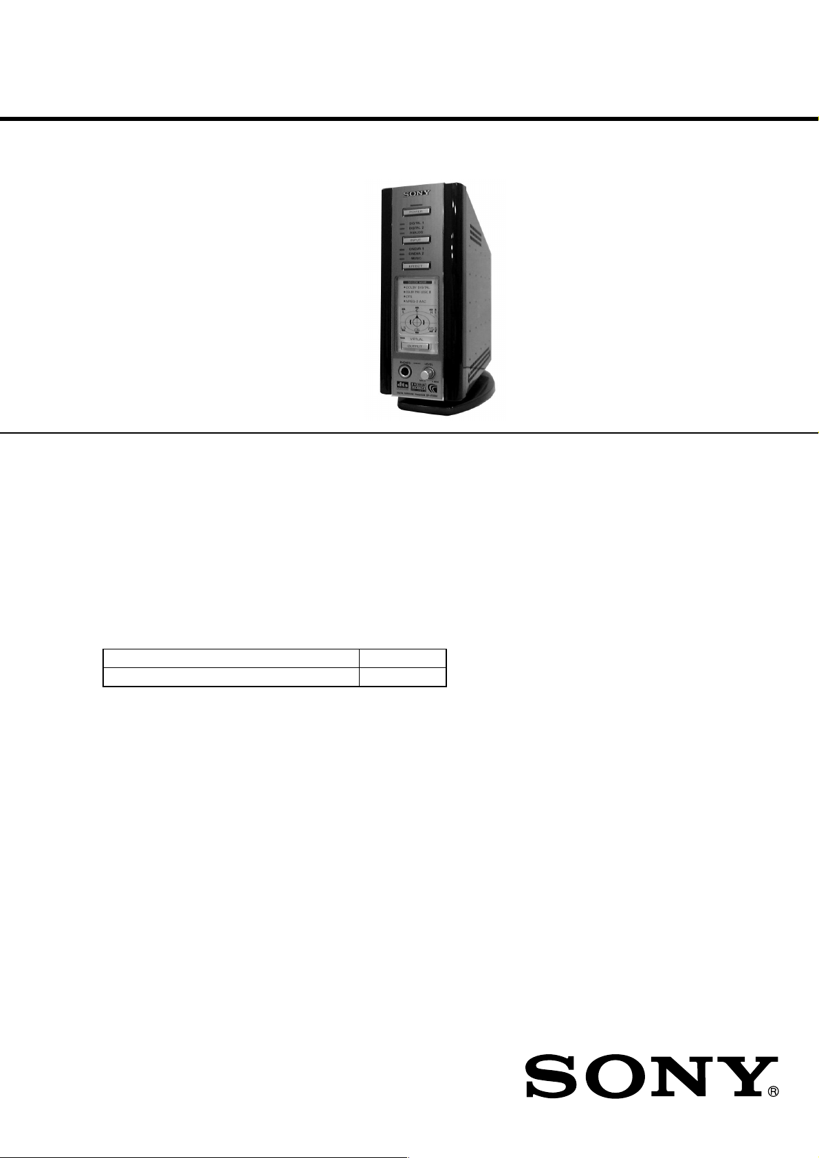
LOCA TING THE CONTROLS
Front Panel of the
Processor
123
POWER
DIGITAL 1
DIGITAL 2
ANALOG
INPUT
CINEMA 1
CINEMA 2
MUSIC
EFFECT
DECODE MODE
DOLBY DIGITAL
DOLBY PRO LOGIC II
DTS
MPEG-2 AAC
C
R
L
LS RS
CS
VIRTUAL
OUTPUT
PHONES LEVEL
MIN MAX
1
5
8
6
7
SECTION 1
GENERAL
1 DIGITAL 1,2 input indicator
ANALOG input indicator
INPUT button
Press to select the input source (DIGITAL
1/DIGITAL 2/ANALOG).
2 POWER indicator
This indicator lights green when you
turn on the processor.
POWER switch
Press to turn on and off the processor.
3 CINEMA 1,2 indicator
MUSIC indicator
EFFECT button (see page 20
details)
Press to select the sound field (CINEMA
1/CINEMA 2/MUSIC).
4 Decode mode indicator (see page
19 for details)
5 PHONES jack (see page 20, 24 for
details)
Connect your headphones to this jack.
Connect the MDR-F1 headphone (sold
separately) for optimum surround effect.
6 PHONES — LEVEL control
Turn to adjust the volume of the
headphones (sold separately) connected
to the PHONES jack.
7 OUTPUT button
Press to select the output mode (OFF/
VIRTUAL FRONT/VIRTUAL
SURROUND).
8 Infrared emitter
Set the emitter in a position so that there
is a straight, unobstructed path to the
sensor.
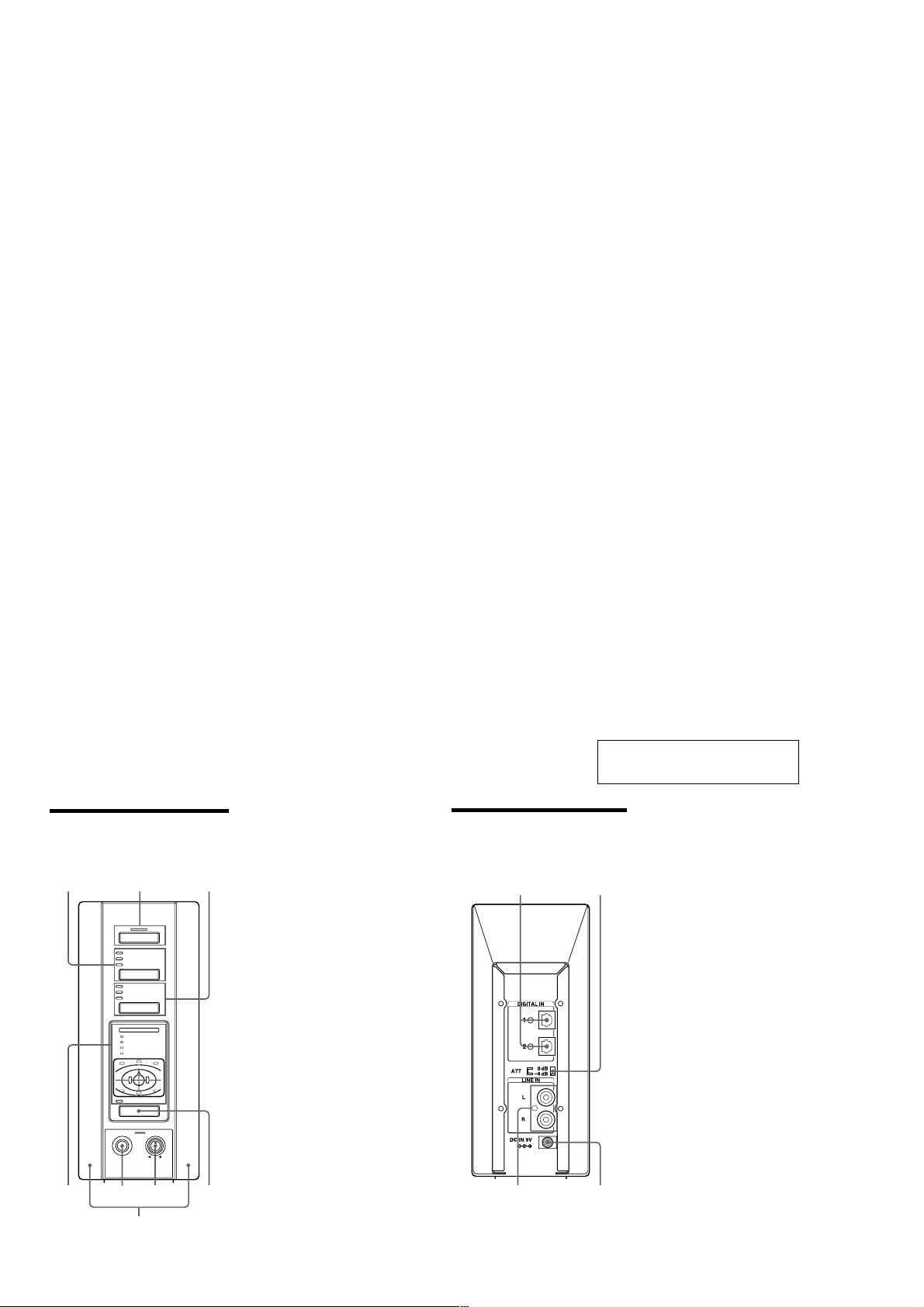
for
Rear Panel of the
Processor
12
34
This section is extracted from
instruction manual.
1 DIGITAL IN 1,2 jack (see page 13 for
details)
Connect a DVD player, Digital TV,
Digital Broadcasting Satellite Receiver,
LD player, or other digital component
(sold separately) to this jack.
2 ATT (attenuator) switch
Set this switch to 0dB when the volume is
too low at analogue input. Normally, this
switch should be set to –8dB.
3 LINE IN jack (see page 14 for details)
Connect the audio output jack on audio/
video equipment (sold separately), such
as a video cassette player or TV, to this
jack.
4 DC IN jack
Connect the supplied AC power adaptor
to this jack. (Be sure to use the supplied
AC power adaptor. Using products with
different plug polarity or other
characteristics can cause a malfunction.)
2
DP-IF8000
L
2
3
46
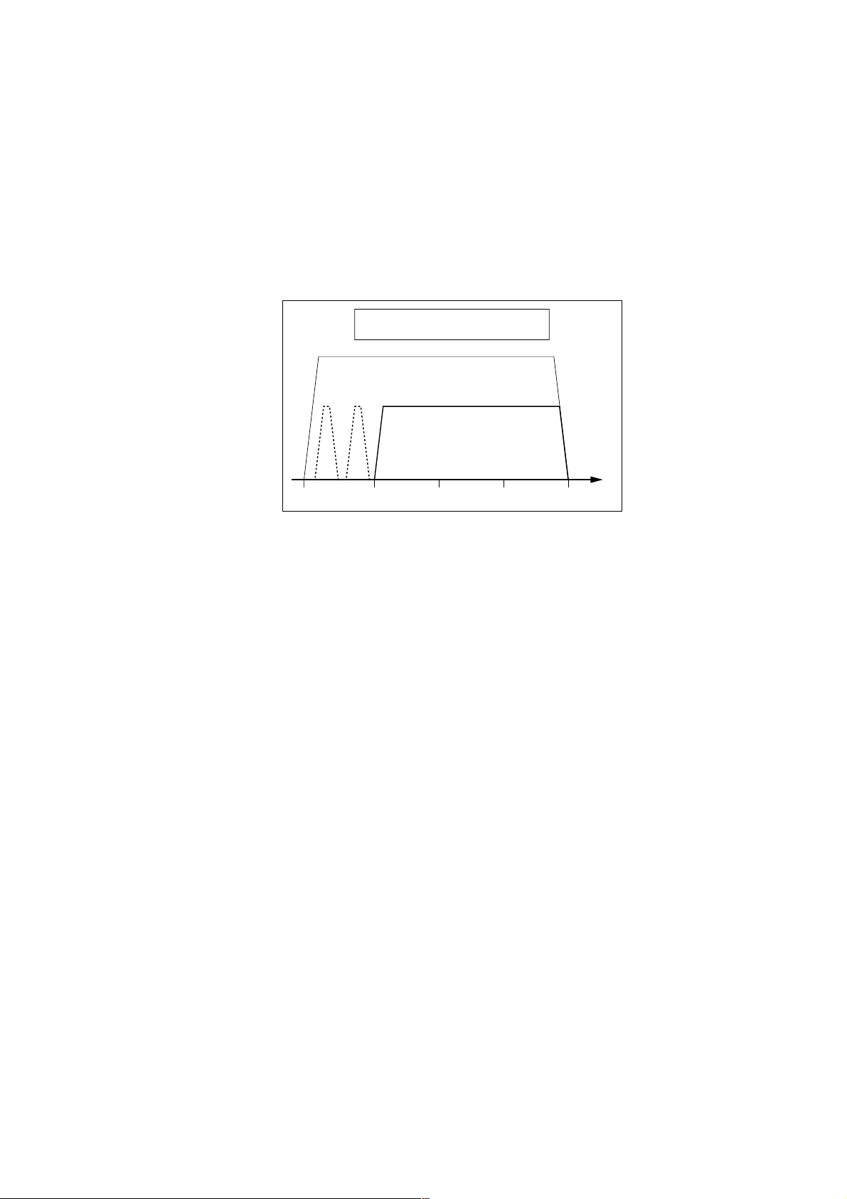
Hi-Fi audio data transmission bandwidth
(2 to 6 MHz)
Analog transmission
Digital transmission (DIAT)
[MHz]
R
5
SECTION 2
SERVICING NOTES
DIAT
(DIGITAL INFRARED AUDIO TRANSMISSION)
High quality media such as DVD and digital broadcasts are currently going through a phase of explosive expansion. To convey these kinds
of high quality media to listeners with no loss in sound nuance or quality, a new technology called DIAT has been developed using the MDRDS8000 to transmit these digital audio signals by infrared without harmful data compression.
DIAT technology allows transmitting digital audio signals without data compression on a portion of the sub-carrier frequency bandwidth
allotted to distributing high-fidelity audio by the IEC (International Electrotechnical Commission) and JEIT A (Japan Electronic Information
Technical Association). The transmission quality is equal to or better than that on compact discs (CD). (Fig. 2-6)
Fig. 2-6 Signal spectrum for digital infrared transmission
[Reference Data]
Sub-carrier frequency : 4.5 MHz
Occupied bandwidth : 2.5 MHz (approx.)
Data rate : 3 Mbps (approx.)
Modulation method : DQPSK
(differential quadrature phase shift keying)
Transmit error correction : Reed Solomon coding
DIGITAL INFRARED AUDIO TRANSMISSION
Along with developing a custom IC, the number of light-emitter elements were doubled (to 16) and light-receiver elements increased 6-fold
(to 24) to achieve a carrier-to-noise signal ratio well capable of transmitting wide-band digital signals. Using digital transmission eliminates
the transmission hiss noise heard in conventional analog broadcasts and allows listeners to enjoy hearing even small sounds.
3
DP-IF8000
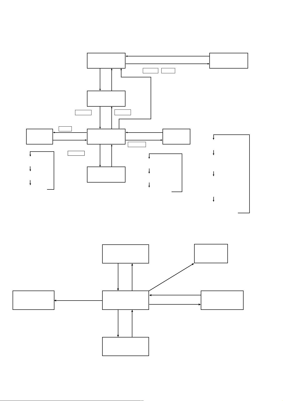
1. STATUS TRANSITION DRAWING
1.1 Processor
ALL POWER OFF
(LEDs all off)
Unplug the AC adapter
Connect AC adapter while simultaneously
pressing POWER & INPUT
TEST
MODE
INPUT
CHANGE
Digital input 1 enabled
(L-DIGITAL 1 lights up)
Digital input 2 enabled
(L-DIGITAL 2 lights up)
Analog input enabled
(L-ANALOG lights up)
Connect the AC adapter
INPUT key
After operation change
Press EFFECT key
while in Virtual output
mode
Unplug the AC
adapter
POWER OFF
(LEDs all light up)
POWER keyPOWER key
POWER ON
(operation LED lights up)
After operation
change
EFFECT
CHANGE
Unplug the AC adapter
After operation change
OUTPUT key
CINEMA1 sound effect
(L-CINEMA1 lights up)
CINEMA2 sound effect
(L-CINEMA2 lights up)
MUSIC sound effect
(L-MUSIC lights up)
OUTPUT
CHANGE
OFF out put
(L-HLch, L-HRch lights up)
Virtual front output
(L-FLch, L-FRch, L-VIRTUAL
lights up)
5.1ch virtual output
(L-FLch, L-FCch, L-FRch
L-SLch, L-SRch, L-VIRTUAL
lights up)
6.1ch virtual output
(L-FLch, L-FCch, L-FRch
L-SLch, L-SCch, L-SRch,
L-VIRTUAL lights up)
1.2 Headphones
LOW BATTERY
operation
When virtual output (processor output)
is changed or S-HT changed while S-HT
is enabled.
Place headphones on head.
When LOW BATTERY
is detected
• Virtual output (head trcking on)
• Virtual output (head trcking off)
POWER OFF
(L-POWER off)
Remove headphones
POWER ON
(L-POWER lights up)
After operation change
EFFECT
CHANGE
Processor infrared ray output to
OFF at transmit limit or cutoff.
After operation change
When switched to stereo-thru
output (processor output)
Receive error
operation
EFFECT
CHANGE
Through output
(head tracking off)
4
DP-IF8000
2. WAVEFORMS & TIMING OF MAIN SIGNAL LINES
2.1 Processor
2.1.1 Audio system
Note: Switch to Digital Input mode by connecting the optical cable
to DIGITAL IN 1 or 2, and pressing the INPUT key.
Switch to Analog Input mode by connecting the audio cable
to LINE IN, and pressing the INPUT key.
• Master clock
MCK (IC12-104pin) : 12.288 MHz (fixed)
MCKADDA (IC5-6pin) : 12.288 MHz (fixed) when in analog
input mode;
When in Digital Input mode, 12.288 MHz for an input source
sampling frequency of 48 kHz.
11.298 MHz for an input sampling frequency of 44.1 kHz; 8.192
MHz for an input sampling frequency of 32 kHz
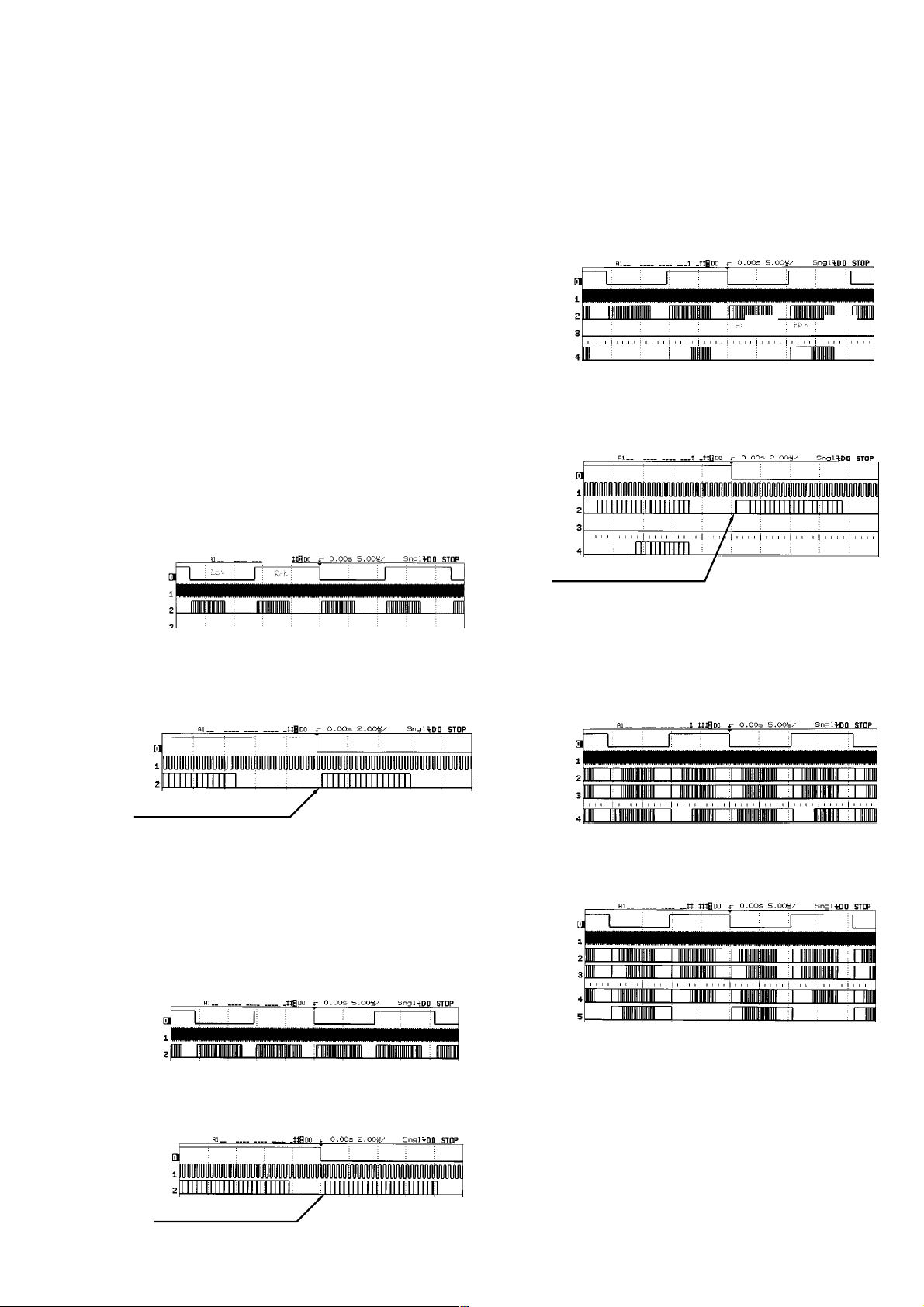
• DIR-DECODER period
Check LRCK (IC11-12pin), BCK (IC 11-14pin), INDATA (IC1110pin).
At power-ON, and in Digital Input mode, any playback source is
okay.
Monitor view is shown in Fig. 1 and detailed timing is shown in
Fig. 2.
LRCK
BCK
INDATA
Note 1: Example shows 44.1 kHz for LRCK; 48 kHz and
32 kHz are also used.
Lch Rch
Fig1
• DECODER-MAIN DSP period
Check LRCK (IC11-12pin), BCK (IC 1 1-14pin), FLRSG (IC11-4pin),
SLRSG (IC11-5pin), CLFSG (IC11-6pin), OTHSG (IC11-7pin).
The playback source at power-ON, and Digital Input mode is Dolby
Digital or DTS, or a 5.1ch source for MPEG-AAC.
The view on the monitor when OFF or VIRTUAL FRONT is selected with the OUTPUT key is shown in Fig. 5. The detailed timing
is shown in Fig. 6.
LRCK
BCK
FLRSG
SLRSG
FLch FRch
CLFSG
Note 3: Example shows 48 kHz for LRCK, but 44.1 kHz and
LFE
32 kHz may also be used.
Fig 5
LRCK
BCK
FLRSG
SLRSG
CLFSG
1 bit offset (I2S format)
Fig 6
Fig. 7 shows the monitor view when VIRTUAL 5.1 is selected with
the OUTPUT key. (Detailed timing is the same as in Fig. 6.)
Fig. 8 shows the monitor view when VIRTUAL 6.1 is selected with
the OUTPUT key. (Detailed timing is the same as in Fig. 6.)
LRCK
BCK
INDATA
1 bit offset (I2S format)
16 bit
Fig 2
• ACD-DECODER period
Check LRCK (IC11-12pin), BCK(IC 11-14pin), INDATA (IC1110pin).
At power-ON, and in Digital Input mode, any playback source is
okay.
Monitor view is shown in Fig. 3 and detailed timing is shown in
Fig. 4.
LRCK
Lch
Rch
BCK
INDATA
Note 2: LRCK is fixed at 48 kHz.
Fig 3
LRCK
BCK
INDATA
1 bit offset (I2S format)
24 bit
Fig 4
LRCK
BCK
FLRSG
SLRSG
CLFSG
FL FR
SL
C
SR
LFE
Note 3: Example shows 48 kHz for LRCK, 44.1 kHz and
32 kHz are also used.
Fig 7
LRCK
BCK
FLRSG
SLRSG
CLFSG
OTHSG
FL FR
SL
C
CS
SR
LFE
Note 3: Example shows 48 kHz for LRCK, 44.1 kHz and
32 kHz are also used.
Fig 8
• MAIN DSP-DAC period
Check LRCK (IC5-5pin), BCK (IC5-4pin), VPOUT2 (IC15-3pin).
At power-ON, and Digital Input mode or Analog Input mode, any
playback source is okay.
A monitor view is shown in Fig. 9 and the detailed timing is shown
in Fig. 10.
5
DP-IF8000
LRCK
BCK
LPOUT2
Note 3: Example shows 48 kHz for LRCK, 44.1 kHz and
32 kHz are also used.
Lch Rch
Fig 9
2.1.2 System Control
Note: Input a signal of some kind to DIGITAL IN 1 and LINE IN.
• MICON-DIR period
Check the DIR_XCS (IC4-37pin), SCK2 (IC4-38pin), and SDO2
(IC4-36pin).
Figure 14 shows the view on the monitor after power is turned on,
at the instant of switching with the INPUT key.
LRCK
BCK
VPOUT2
Fig 10
• MAIN DSP-DIAT period
Check RCS (IC12-109pin), BCK (IC12-106), VPOUT1 (IC1296pin), RINFO (IC12-107pin).
Turn the power on, set in Digital Input mode, and select VIRTUAL
FRONT, or VIRTUAL 5.1 or VIRTUAL 6.1 with the OUTPUT
switch.
The view on the monitor when the input source sampling frequency
is 48 kHz is shown in Fig. 11.
The view on the monitor when the input source sampling frequency
is 44.1 kHz is shown in Fig. 12.
The view on the monitor when the input source sampling frequency
is 32 kHz is shown in Fig. 13.
RCS
BCK
VPOU1
RINFO
Note 4: fs=48kHz
0001000 t fs=48k
Fig 11
RCS
BCK
VPOU1
RINFO
Note 5: fs=44.1kHz
0000000 t fs=44.1k
Fig 12
RCS
BCK
VPOU1
RINFO
Note 6: fs=32kHz
0011000 t fs=32k
Fig 13
DIR_XCS
SCK
(500KHZ)
SDO2
Address
8 bit
data
8 bit + 8 bit
00010111
Fig 14
• MICON-DAC period
Check the DAC_XCS (IC5-10pin), SCKO (IC5-8pin), and SDO02
(IC5-9pin).
Figure 15 shows the view on the monitor after power is turned on,
at the instant of switching with the INPUT key.
DAC_XCS
SCK 0
(500KHZ)
SDO 0
Address
8 bit
data
8 bit + 8 bit
00100000
Fig 15
• MICON-LED DRIVER period
Check the LED_XLAT (CN102-3pin), SCKO(CN102-6pin), and
SDO(CN102-7pin).
Figure 16 shows the view on the monitor after power is turned on,
at the instant of switching with each key.
LED_XLAT
SCK 0
(500KHZ)
SDO 0
after data transfer
8 bit + 8 bit
Fig 16
LAT
• MICON-DIAT period
Check the DIAT_LAT (IC12-152pin), SCKO (IC12-151pin), SDO
(IC12-153pin).
Figure 17 shows the view on the monitor after power is turned on,
at the instant of switching with the INPUT key . The timing is shown
in detail in FIG. 18.
When OFF is selected with the OUTPUT key, check the DILRCK
(IC12-98pin), BCK (IC12-106pin), VPOUT1 (IC12-96pin), and the
view on the monitor should be the same as the MAIN DSP-DAC
period.
6
DIAT_LAT
SCK 0
SDO 0
DIAT_LAT
SCK 0
(500KHZ)
SDO 0
Fig 17
after 24bit data transfer LAT
Fig 18
• MICON-DECODER period
Fig 22
LRCK/RCS
BCK
DIAT_OUT
RINFO
0001000 t fs=48kNote 7: fs=48kHz
Fig 26
LRCK/RCS
BCK
DIAT_OUT
RINFO
Check the DEC_XCS (IC11-2pin), SCK1 (IC1 1-1pin), SDO1 (IC11143pin), SDI1 (IC11-144pin).
Figure 19 shows the view on the monitor after power is turned on,
at the instant of switching with the OUTPUT key. The timing is
shown in detail in FIG. 20.
DEC_XCS
SCK 1
SDO 1
SDI 1
Sending the
24 bit data
Receiving the
24 bit data (example)
Fig 19
DEC_XCS
SCK 1
(1MHz)
SDO 1
SDI 1
Fig 20
• MICON-MAIN DSP period
Check the DSP_XCS (IC19-2pin), SCK1 (IC19-1pin), SDO1 (IC19143pin), and the DSP_XHREQ (IC19-3pin).
Figure 21 shows the view on the monitor after power is turned on,
at the instant of switching with the OUTPUT key. (The detailed
timing is the shown as shown in FIG. 20.
DSP_XCS
SCK 1
(1MHz)
SDO 1
DSP_XHREQ
Start of 24 bit data transfer, at 2nd bit, HREQ t 1
After transfer of 24 bit data, HREQ t 0
DP-IF8000
LRCK/RCS
BCK
DIAT_OUT
RINFO
Note 8: fs=44.1kHz
Fig 23
LRCK/RCS
BCK
DIAT_OUT
RINFO
Note 9: fs=32kHz
Fig 24
LRCK/RCS
BCK
DIAT_OUT
RINFO
Note 10: Only LRCK, BCK and DATA are enabled. RINFO
is disabled.
Fig 25
0000000 t fs=44.1k
0011000 t fs=32k
Lch Rch
Fig 21
2.2 Headphones
2.2.1 Audio System
Note: Switch to Digital Input mode by connecting the optical cable
to DIGITAL IN 1 or 2, and pressing the INPUT key.
• Master clock
DSP_MCK(IC501-34pin) : 12.288 MHz (fixed)
DAC_MCK (IC102-2pin) : 12.288 MHz when the input source sampling frequency to the processor is 48 kHz.
11.289 MHz when the sampling frequency is 44.1 kHz
8.192 MHz when the sampling frequency is 32 kHz
• DIAT-DSP period
Check the LRCK/RCS (IC501-94pin), BCK (IC501-6pin),
DIAT_OUT (IC501-20pin), RINFO (IC501-19pin).
Turn the power on, set in Digital Input mode, and select VIRTUAL
FRONT, or VIRTUAL 5.1 or VIRTUAL 6.1 with the OUTPUT
key.
Turn the headphone power on.
The view on the monitor when the input source sampling frequency
to the processor is 48 kHz is shown in Fig. 22.
The view on the monitor when the input source sampling frequency
to the processor is 44.1 kHz is shown in Fig. 23.
The view on the monitor when the input source sampling frequency
to the processor is 32 kHz is shown in Fig. 24.
The view on the monitor when OFF is selected with the OUTPUT
key is shown in Fig. 25. The detailed timing is shown in Fig. 26.
• DSP-DAC period
Check the LRCK (IC102-16pin), BCK (IC102-14pin), and
DSP_OUT (IC102-15pin).
Turn on the processor and set to Digital Input mode. Turn on the
headphone power, and apply an input source signal (any kind is
okay) to the processor.
The view on the monitor is shown in Fig. 27, and the detailed timing is shown in Fig. 28.
LRCK
Lch Rch
BCK
DSP_OUT
Fig 27
LRCK
BCK
DSP_OUT
1 bit offset (I2S format)
Fig 28
7
DP-IF8000
2.2.2 System Control
• MICON-DSP period
Check the DSP_XCS (IC501-23pin), SCK (IC501-26pin), SDO
(IC501-24pin), and XHREQ (IC501-27pin).
The view after turning on the headphone power is shown in Fig. 29,
and the detailed timing is shown in Fig. 30.
DSP_XCS
SCK
SDO
XHREQ
Fig 29
DSP_XCS
SCK
(625kHz)
SDO
XHREQ
Start of 24 bit data transfer, at 2nd bit, HREQ t 1
After transfer of 24 bit data, HREQ t 0
Fig 30
• DIAT-MICON-DSP period
Check the DTQ (IC901-28pin), DSP_DTQ (IC501-28pin), ARDET
(IC901-27pin), DIAT_DTSEL (IC101-16pin).
Turn on the processor and set to Digital Input mode. Turn on the
headphone power, and apply an input source signal (any kind is
okay) to the processor.
The instant when switching from OFF to VIR TUAL FRONT using
the processor OUTPUT key is shown in Fig. 31.
The monitor view at the instant when switching from VIRTUAL
FRONT to VIRTUAL 5.1 or from VIRTUAL 5.1 to VIRTUAL 6.1
with the processor OUTPUT key is shown in Fig. 32.
The monitor view at the instant when switching from VIRTUAL
5.1 or VIRTUAL 6.1 to OFF with the processor OUTPUT key is
shown in Fig. 33.
DTQ
DSP_DTQ
ARDET
DIAT_DTSEL
*1 Pulse output when set to DIAT receive mode.
*2 ARDET = 1 t VIRTUAL mode
ARDET = 0 t OFF mode
*3 Approximately 25 msec from lock report to DSP until DIAT
receive mode is set.
DTSEL t VIRTUAL mode
DTSEL = 0 t OFF mode
Infrared unlock
(receive NG)
Infrared lock (receive OK)
Report lock to DPS
DSP identifies processor
transmit mode *2
Fig 31
*1
Set DIAT receive
mode *3
DTQ
DSP_DTQ
ARDET
DIAT_DTSEL
DTQ
DSP_DTQ
ARDET
DIAT_DTSEL
8
Fig 32
Fig 33
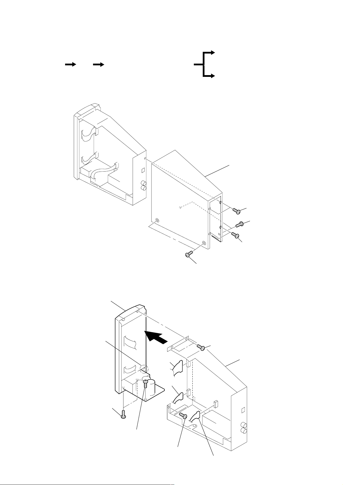
• This set can be disassembled in the order shown below.
)
DP-IF8000
SECTION 3
DISASSEMBLY
TX board
Set
Note: Follow the disassembly procedure in the numerical order given.
Cover
Chassis (processor), “Panel ASSY, front”
3-1. COVER
LED board, AMP board
5
Cover
3
Two screws (+BVTT 2.6X5)
2
Two screws (+BVTT 2.6X5)
3-2. CHASSIS (PROCESSOR), “PANEL ASSY, FRONT”
Panel ASSY, front
3
CN102
9
2
CN002
8
Claw
5
T wo screws(+P)
4
1
Two screws (+BVTT 2.6X5)
4
Two screws (+P 3X8)
Chassis (processor
Two screws (+BVTT 2.6X5)
6
Screw (+BTT)
7
Screw (+P 3X8)
1
CN001
9
DP-IF8000
d
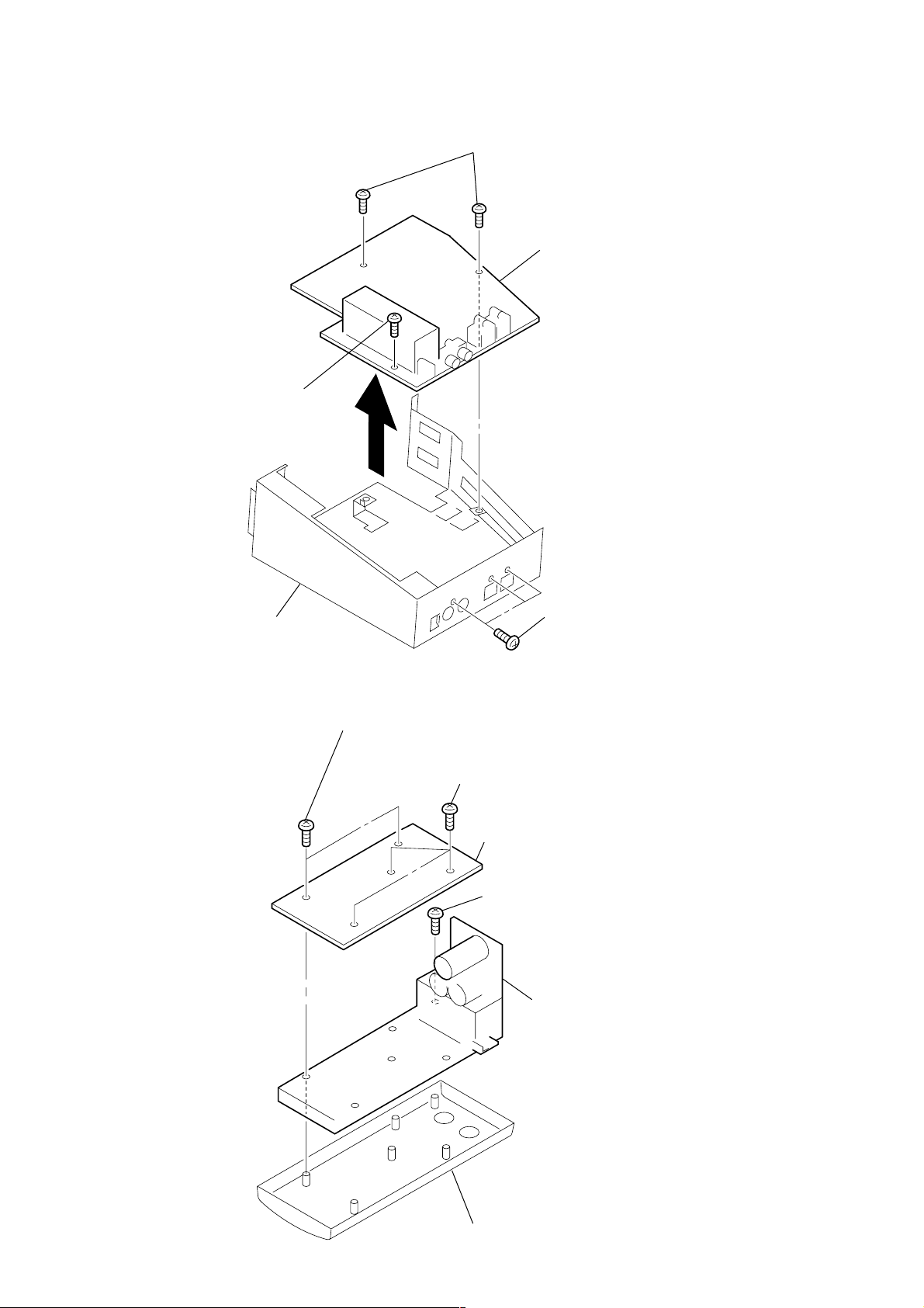
3-3. TX BOARD
2
Screw
3
Two screws (+BTT)
TX board
Chassis (processor)
3-4. LED BOARD, AMP BOARD
1
Two screws (+P 2X8)
1
Three screws (+P 3X8)
2
Three screws (+P 2X8)
3
LED board
4
Screw (+P 2X8)
5
AMP boar
10
Panel ASSY, front
SECTION 4
TEST MODE
DP-IF8000
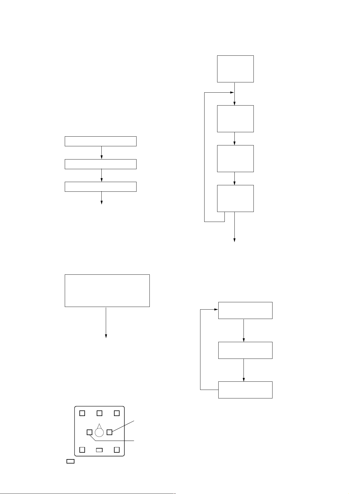
1. OVERVIEW
The internal microprocessor in this device has a test mode that can
perform all checks. Items that must be checked during repairs are
stored in this microprocessor.
2. SETTING THE TEST MODE
To call up test mode, turn on the power while holding down the
POWER and INPUT keys. (Connect the AC adapter.)
3. CANCEL THE TEST MODE
Remove the AC adapter.
4. TEST MODE
4-1. LED check
LEDs light up in sequence *1)
EFFECT key
All LEDs light up *2)
EFFECT key
All LEDs turn off *3)
Power key
To Key check
5. TEST TONE OUTPUT
DIGITAL1
L, R, HL, HR
LED lights up
INPUT key
DIGITAL2
L, R, HL, HR
LED lights up
INPUT key
ANALOG
L, R, HL, HR
C LED lights up
EFFECT key
CINEMA1
L, R, HL, HR
R LED lights up
POWER key
1kHz, 0dBv L&R ch
*6)
1kHz, –10dBv L&R ch
*6)
100Hz, –10dBv L&R ch
*6)
10kHz, –10dBv L&R ch
*6)
*1) Test mode setup status
*2) Infrared LEDs shall light up
*3) Infrared LEDs shall turn off
4-2. Key Check
Pressing the INPUT, EFFECT or
OUTPUT key lights up the matching
LED *4)
To test tone output
*4) Matching LED
POWER key : POWER LED, WINDOW LED
INPUT key : DIGITAL1, DIGITAL2,
ANAGOG LED
EFFECT key : CINEMA1, CINEMA2,
MUSIC LED
OUTPUT key : DECODE MODE LED
*5) Decode mode LED
POWER key
INPUT key
Shift to normal power-on operation
*6) Pressing the OUTPUT key in each test mode changes
the output channels as shown below.
(e.g.) During L&R channel output at 1 kHz and 0dBv.
End test mode
DIGITAL1
L, R, HR LED lights up
DIGITAL1
L, R LED lights up
DIGITAL1
HL, HR LED lights up
L&R ch output
L ch ouput
(R ch MUTE)
R ch output
(L ch MUTE)
L
LS
VIRTUAL
CS
C
R
RS
HR LED
HL LED
11
DP-IF8000
0
SECTION 5
ELECTRICAL ADJUSTMENT
1. CAUTION
1. Perform adjustment in sequence as listed.
2. Apply a 9 volt DC supply voltage.
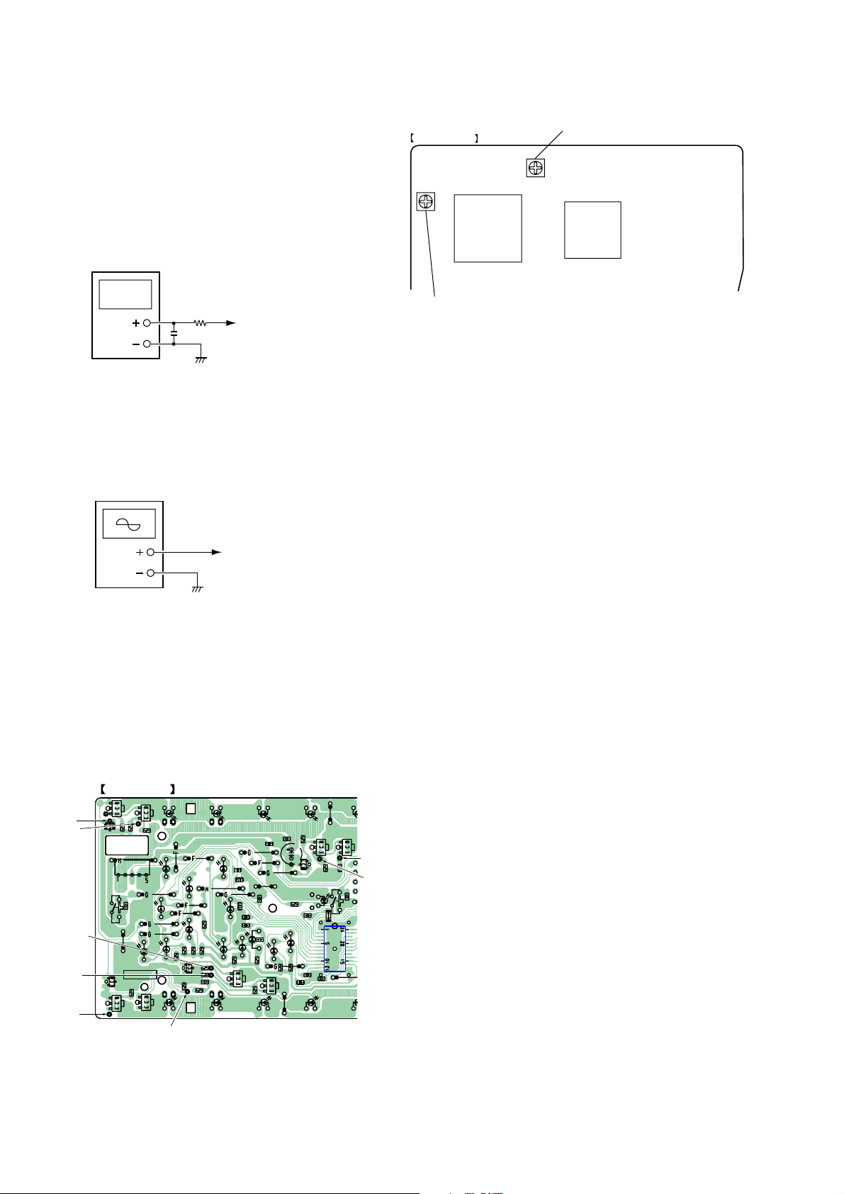
2. DC BIAS ADJUSTMENT
Connect a digital voltmeter to test points TP119, 121, 125, 127,
130, 131, 133, 134 on the LED board. Adjust RV101 on the TX
board to obtain an output voltage of 480 ± 5mV on the TX board.
digital voltmeter
10k
Ω
TP119,121,125,127,
130,131,133,134
0.1
µ
ceramic
3. RF level alignment
Connect an oscilloscope to test points TP119, 121, 125, 127,
130, 131, 133, 134 on the LED board. Adjust RV201 on the TX
board to obtain an output waveform of 960±5mVp-p.
oscilloscope
• Adjustment location:
TX BOARD (SIDE A)
IC12
RV101: DC BIAS alignment
RV201: RF LEVEL alignment
IC19
TP119,121,125,127,
130,131,133,134
Note: Use an oscilloscope with a bandwidth of at lest 200 MHz.
4. RECHECK
The DC bias adjustment made above in 2. may sometime change
(deviate) after the RF level adjustment is made above in 3. So
recheck that the DC bias is at the correct level after making the
RF level alignment. If the DC bias has deviated, realign by repeating the adjustment in 2. and 3. above.
• Connection points :
TP121
TP119
TP134
TP133
TP131
LED BOARD
1
5
3
Q
TP121
4
5
3
Q
7
5
8
8
R
R
JW214
CN903
7
4
0
2
W
C
S
D221
VERTUAL
6
5
3
3
Q
5
3
Q
0
1
1
R
TP131
TP119
7
5
3
Q
9
8
R
5
1
2
D
JW
215
6
1
2
D
JW216
JW
217
1
7
3
2
1
1
2
2
2
D
D
R
9
5
3
Q
TP130
(pattern)
5
6
D
D
JW222
3
1
2
JW
8
1
2
D
JW
224
JW
223
7
1
9
2
1
R
2
D
6
4
1
1
2
2
R
R
2
1
2
R
R112
2
6
TP134
3
Q
TP133
R111
7
2
4
2
C
0
1
TP130
R
4
1
3
1
1
R
D
9
7
D
C301
2
1
2
D
JW
225
4
1
2
D
3
1
2
1
D
1
2
R
4
1
D
C241
JW
218
JW211
C225
JW
212
C224
JW
227
JW
226
3
2
2
C
6
2
2
C
C227
9
0
C228
2
D
C229
0
1
1
8
9
1
2
0
0
0
2
D
1
2
2
D
2
R
R
R
JW
209
0
6
3
3
Q
1
1
1
6
3
R
Q
0
2
2
5
1
D
JW
4
8
0
D
2
D
JW
2
2
0
8
5
1
5
3
3
R
Q
0
3
2
C
TP127
C210
TP125
1
0
1
R
0
2
2
D
7
1
1
JC
IC206
9
3
2
C
Q
0
0
1
3
R
W
S
6
0
2
C
0
9
2
C
JW221
7
1
D
1
5
3
C
5
5
3
Q
R215
8
0
2
D
C231
6
1
D
TP125
TP127
12
 Loading...