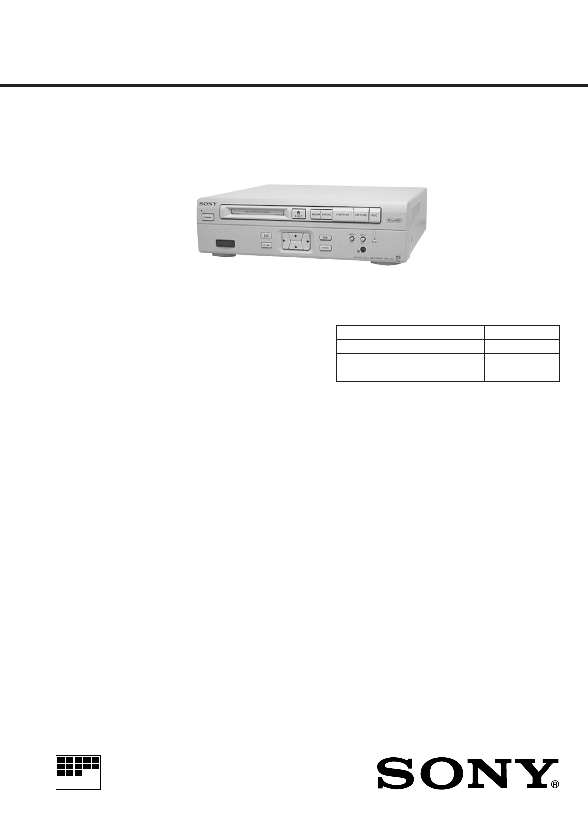
DPA-300
MICROFILM
SERVICE MANUAL
U.S and foreign patents licensed from Dolby Laboratories
Licensing Corporation.
SPECIFICATIONS
US Model
Canadian Model
Model Name Using Similar Mechanism NEW
MD Mechanism Type MDM-2BR
Base Unit Name MBU-2
Optical Pick-up Name KMS-210A/J-N
System
Recording format Picture MD recording system
Data compression/saving system
JPEG
FINE mode : 128kB
(the maximum 1,000 images)
STANDARD mode : 64kB
(the maximum 2,000 images)
Revolutions 400 rpm to 900 rpm (CLV)
Error correction Advanced Cross Interleave Reed
Solomon Code (ACIRC)
Laser Semiconductor laser ( λ = 780 nm)
Emission duration : continuous
Laser output Max 44.6 µW
* This output is the value measured at a
distance of 200 mm from the objective lens
surface on the Optical Pick-up Block with
7 mm aperture.
Sampling frequency 44.1 kHz
Coding Adaptive TRansform Acoustic Coding
(A TRAC)
Modulation system EFM (Eight to Fourteen Modulation)
Number of channels 2 stereo channels
Input VIDEO INPUT
Input signal : 1Vp-p
(75 Ω unbalanced)
Y/C INPUT, Mini DIN 4-pin
Luminance signal : 1Vp-p
(75 Ω unbalanced)
Chrominance signal : 0.286 Vp-p
(75 Ω unbalanced)
AUDIO IN (L/R)
Input level : 2 Vrms (full bit)
Input impedance : more than 47 kΩ
FS1/FS2 (RED/WHITE) connectors
Output VIDEO OUTPUT
Output signal : 1 Vp-p
(75 Ω unbalanced)
Y/C OUTPUT, Mini DIN 4-pin
Luminance signal : 1 Vp-p
(75 Ω unbalanced)
Chrominance signal : 0.286 Vp-p
(75 Ω unbalanced)
AUDIO OUT (L/R)
Output level : 2 Vrms (full bit)
Output impedance : more than 47 kΩ
— Continued on next page —
DIGITAL STILL RECORDER
SAFETY CHECK-OUT
General
Power requirements Sony AC Power Adaptor AC-DA300
(supplied) connected at the DC IN 12 V
Power consumption 20 W
Operating temperature 5 °C to 35 °C (41°F to 95°F)
Operating humidity 30% to 85%
Dimensions Approx. 280 × 80 × 290 mm
Mass Approx. 2.5 kg (5 lb. 8 oz)
Supplied accessories AC power adaptor AC-DA300
Design and specifications are subject to change without notice.
jack : 120V AC, 60Hz (US model)
1
(11
/8 × 31/4 × 111/2 inches)
(w/h/d, including projecting parts and
controls)
Remote commander RMT-DA300 (1)
Size AA (R6) batteries (2)
CAUTION
Use of controls or adjustments or performance of procedures
other than those specified herein may result in hazardous
radiation exposure.
Notes on chip component replacement
• Never reuse a disconnected chip component.
• Notice that the minus side of a tantalum capacitor may be
damaged by heat.
After correcting the original service problem, perform the following
safety checks before releasing the set to the customer:
Check the antenna terminals, metal trim, “metallized” knobs, screws,
and all other exposed metal parts for AC leakage. Check leakage as
described below.
LEAKAGE
The AC leakage from any exposed metal part to earth ground and
from all exposed metal parts to any exposed metal part having a
return to chassis, must not exceed 0.5 mA (500 microamperes).
Leakage current can be measured by any one of three methods.
1. A commercial leakage tester, such as the Simpson 229 or RCA
WT -540A. Follow the manufacturers’ instructions to use these
instruments.
2. A battery-operated AC milliammeter. The Data Precision 245
digital multimeter is suitable for this job.
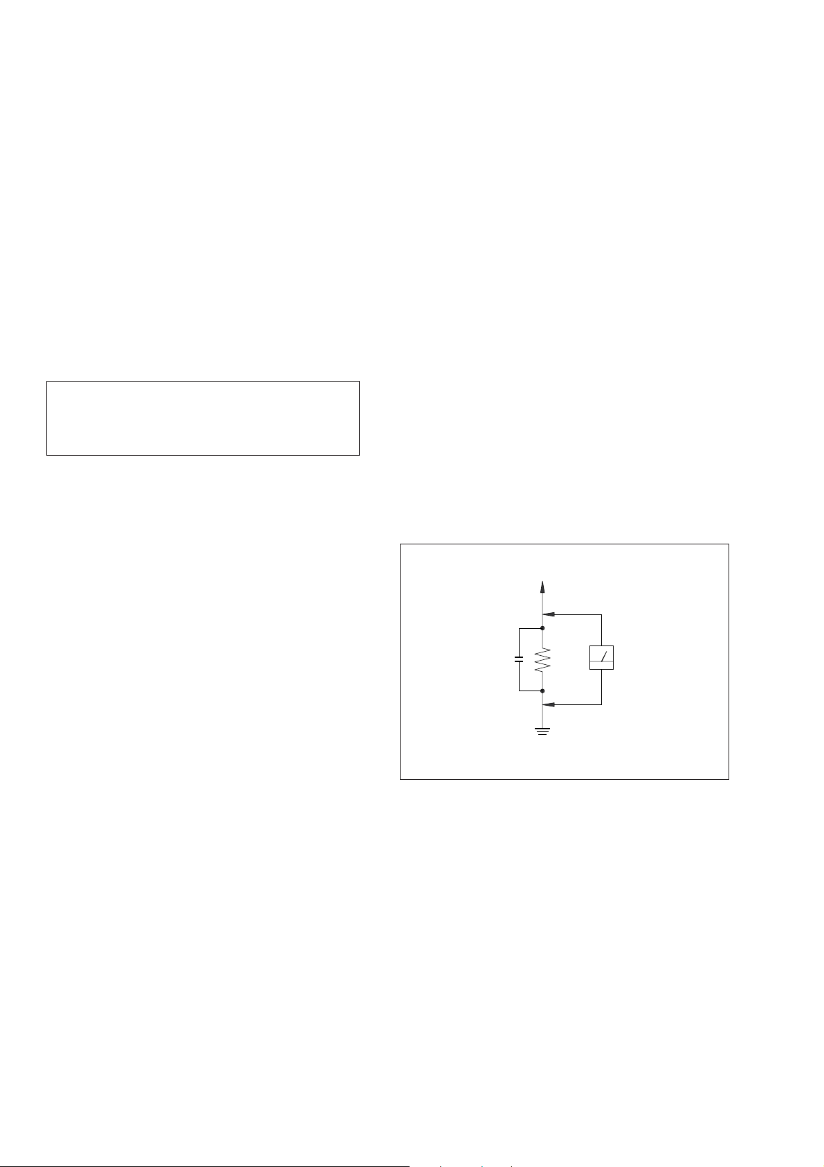
3. Measuring the voltage drop across a resistor by means of a
VOM or battery-operated AC voltmeter . The “limit” indication
is 0.75 V, so analog meters must have an accurate low-voltage
scale. The Simpson 250 and Sanwa SH-63Trd are examples of
a passive VOM that is suitable. Nearly all battery operated
digital multimeters that have a 2V AC range are suitable. (See
Fig. A)
Flexible Circuit Board Repairing
• Keep the temperature of soldering iron around 270˚C
during repairing.
• Do not touch the soldering iron on the same conductor of the
circuit board (within 3 times).
• Be careful not to apply force on the conductor when soldering
or unsoldering.
CAUTION
Danger of explosion if battery is incorrectly replaced.
Replace only with the same or equivalent type recommended by
the manufacturer.
Discard used batteries according to the manufacturer’s instructions.
To Exposed Metal
Parts on Set
AC
µ
F 1.5k
0.15
Ω
voltmeter
(0.75V)
Earth Ground
Fig. A. Using an AC voltmeter to check A C leakage.
SAFETY-RELATED COMPONENT WARNING!!
COMPONENTS IDENTIFIED BY MARK ! OR DO TTED LINE WITH
MARK ! ON THE SCHEMATIC DIAGRAMS AND IN THE PARTS
LIST ARE CRITICAL TO SAFE OPERATION. REPLACE THESE
COMPONENTS WITH SONY PARTS WHOSE PART NUMBERS
APPEAR AS SHOWN IN THIS MANUAL OR IN SUPPLEMENTS
PUBLISHED BY SONY.
— 2 —
ATTENTION AU COMPOSANT AYANT RAPPORT
À LA SÉCURITÉ!
LES COMPOSANTS IDENTIFÉS PAR UNE MARQUE ! SUR LES
DIAGRAMMES SCHÉMATIQUES ET LA LISTE DES PIÈCES SONT
CRITIQUES POUR LA SÉCURITÉ DE FONCTIONNEMENT. NE
REMPLACER CES COMPOSANTS QUE PAR DES PIÈSES SONY
DONT LES NUMÉROS SONT DONNÉS DANS CE MANUEL OU
DANS LES SUPPÉMENTS PUBLIÉS PAR SONY.

TABLE OF CONTENTS
1. SERVICING NOTE ··························································4
2. GENERAL ·········································································· 7
3. DISASSEMBLY
3-1. Upper Case ································································· 11
3-2. Front Panel, Panel Board and Video In Board ··········· 11
3-3. Picture Board, Power Board and Mechanism Deck
····················································································12
3-4. MD Mechanism Deck ················································ 13
3-5. Slider (MD Mechanism) ············································13
3-6. MD Base Unit (MBU-2) and Loading Motor Assy ··· 14
3-7. How to Attach the Slider (MD Mechanism) ·············· 14
4. TEST MODE ···································································· 15
5. ELECTRICAL ADJUSTMENTS ······························· 18
6. DIAGRAMS
6-1. Circuit Board Location··············································· 28
6-2. Block Diagram — BD Section —······························ 29
6-3. Block Diagram — MD Control Section — ··············· 31
6-4. Block Diagram — Video Control Section — ············33
6-5. Block Diagram — Video Process Section — ············35
6-6. Block Diagram — IR Section — ······························· 37
6-7. Block Diagram — Video Out Section — ··················· 39
6-8. Block Diagram — Video In Section — ····················· 41
6-9. Block Diagram — Audio Section — ························· 43
6-10. Block Diagram — Power Section — ························· 45
6-11. Printed Wiring Board — Picture Section — ·············· 47
6-12. Schematic Diagram — Picture Section (1/3) — ········ 51
6-13. Schematic Diagram — Picture Section (2/3) — ········ 55
6-14. Schematic Diagram — Picture Section (3/3) — ········ 59
6-15. Printed Wiring Board — BD Section —···················· 62
6-16. Schematic Diagram — BD Section — ······················ 65
6-17. Schematic Diagram — Video In Section — ·············· 69
6-18. Printed Wiring Board — Video In Section — ··········· 73
6-19. Printed Wirimg Board — MD Section —·················· 77
6-20. Schematic Diagram — MD Section (1/2) — ············· 81
6-21. Schematic Diagram — MD Section (2/2) — ············· 85
6-22. Printed Wiring Board — Power Section — ··············· 89
6-23. Schematic Diagram — Power Section — ·················· 91
6-24. Printed Wiring Board — Panel Section — ················ 94
6-25. Schematic Diagram — Panel Section — ··················· 97
6-26. IC Block Diagrams····················································· 99
6-27. IC Pin Function ························································ 111
7. EXPLODED VIEWS
7-1. Upper Case Section ·················································· 144
7-2. Front Panel Section ·················································· 145
7-3. Bottom Cabinet Section ··········································· 146
7-4. Mechanism Section (MDM-2BR)···························· 147
7-5. Base Unit Section (MBU-2)····································· 148
8. ELECTRICAL PARTS LIST ································· 149
— 3 —
SECTION 1
SERVICING NOTE
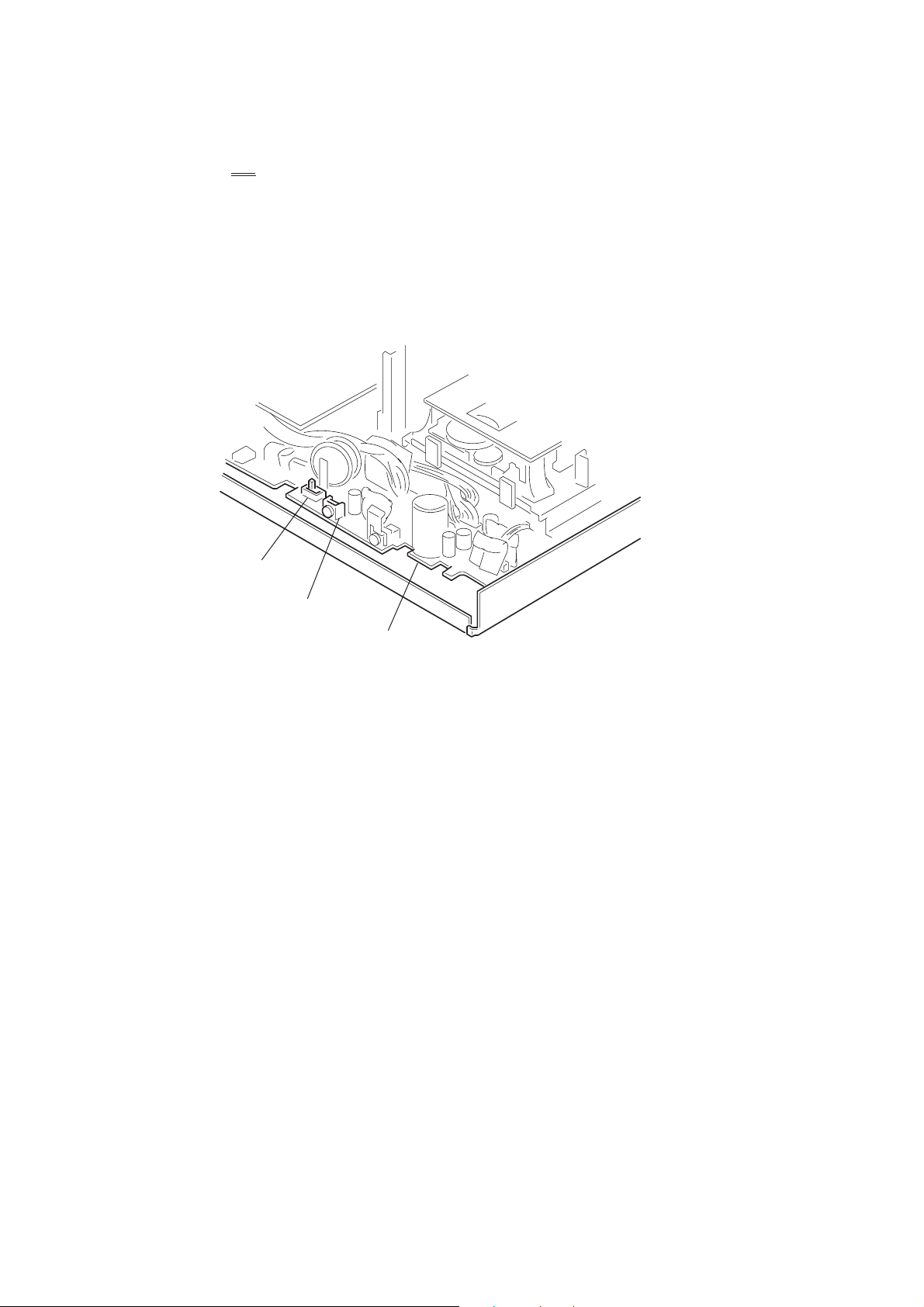
[About Switches on POWER Board]
• Backup Power ON/OFF Switch (S1351 B. UP ON)
Be sure to turn this switch to OFF when removing and inserting connectors to and from the circuit boards.
This switch protects semiconductors from breakdown due to static electricity.
Set this switch to ON during normal operation. The DPA-300 does not work unless this switch is set to ON.
• Reset Switch (S1352 RESET)
This switch resets forcibly system of DPA-300. Press the reset switch when microprocessor runs away, or when DPA-300 does not
operate normally, or when the main power is desired to turn ON, OFF and back ON momentarily during test mode, etc.
Rear Side
S1351
(B.UP ON)
S1352
(RESET)
POWER board
— 4 —
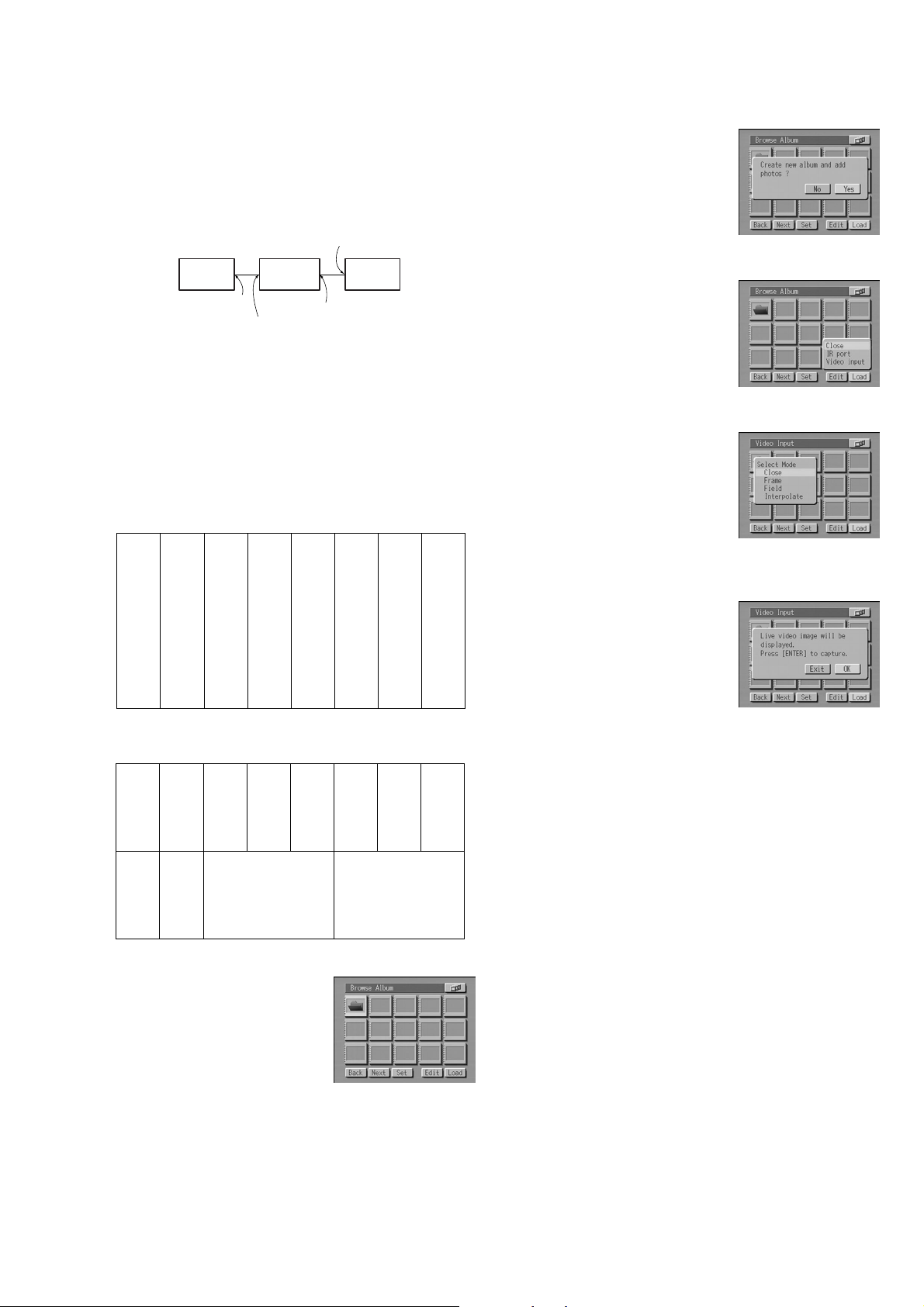
[How to Set the Mode Displaying the Through Picture]
Input the color bar signal and enter this mode as follows to check
the DPA-300 for voltages, waveforms and to implement a part of
adjustments.
Connection:
Color bar generator
DPA-300
Output
Video Input or
S-Video Input
Input
monitor
Video Output
When the equipment connection is completed, set up this mode by
following the procedures in the order given below.
4. Select “Load” using the f F g G button and press the ENTER
button.
The message “Create new album
and add photos?” appears.
5. Select “Yes” using the f F g G button and press the ENTER
button.
The new album to load the pictures
are created. When an album is
created, the loading menu appears.
1. Turn the main power ON. (Turn on the main power of color
bar generator, DPA-300 and monitor.)
2. Connect the color bar signal to video input.
Color bar signal specifications to be input
Color bar signal for voltage and waveform measurement
RED
RED
BLUE
BLUE
BLACK
BLACK
BLACK
CYAN
YELLOW
WHITE (75%)
Color bar signal for adjustment
CYAN
YELLOW
WHITE (75%)
Q
I
WHITE (100%)
GREEN
GREEN
MAGENTA
MAGENTA
6. Select “Video input” using the g G button and press the ENTER
button.
The display from which the modes
can be selected, appears
7. Select “Frame” using the g G button and press the ENTER
button.
Mode differs depending on the type
of input signal supplied from the
video equipment connected.
8. Select “OK” using the f F g G button and press the ENTER
button.
9. Color bars supplied to the Video Input connector, appear on
monitor when the ENTER button is pressed.
Note :When the ENTER button is pressed in the state of step 9, the
picture is loaded and the DPA-300 exits the Through mode.
When the ENTER button is pressed incorrectly, follow the
instruction shown on the monitor screen and return to the
state of step 9.
3. Insert the MD data disc.
List of album appears.
When the MD data disc has not been formatted, format it.
— 5 —
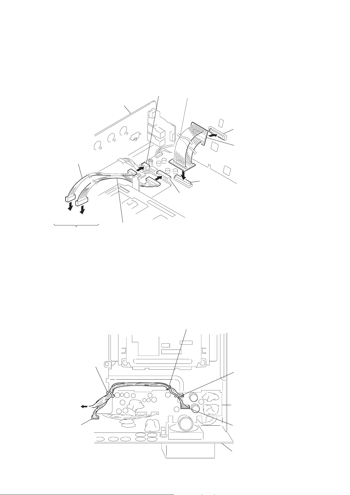
[About Extension Cable]
d
To check the MD board, connect the PICTURE board and the POWER board using the extension cables as shown before starting to check.
CN2007
Extension cable 5p
J-2501-120-A
to CN1004
to CN1001
POWER board
Rear panel
PICTURE board
CN4002
Extension cable 40p
J-2501-122-A
CN2003
CN2006
MD board
Extension cable 10p
J-2501-121-A
[How to Route the Cables]
Be sure to route the cables which connect the POWER board CN1002, CN1006, CN1007 and PICTURE board CN1001 as shown.
Lead pin (LP1003)
Lead pin
(LP1004)
CN1002
to CN1001
on PICTURE board
CN1007
Rear Side
POWER boar
CN1006
Rear panel
— 6 —
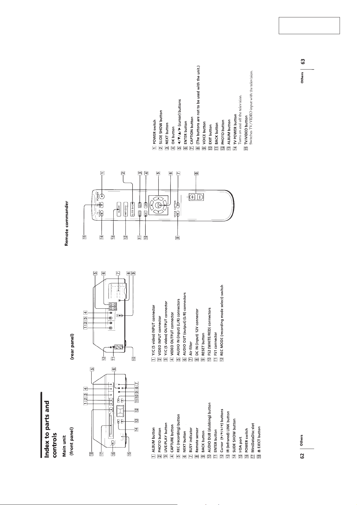
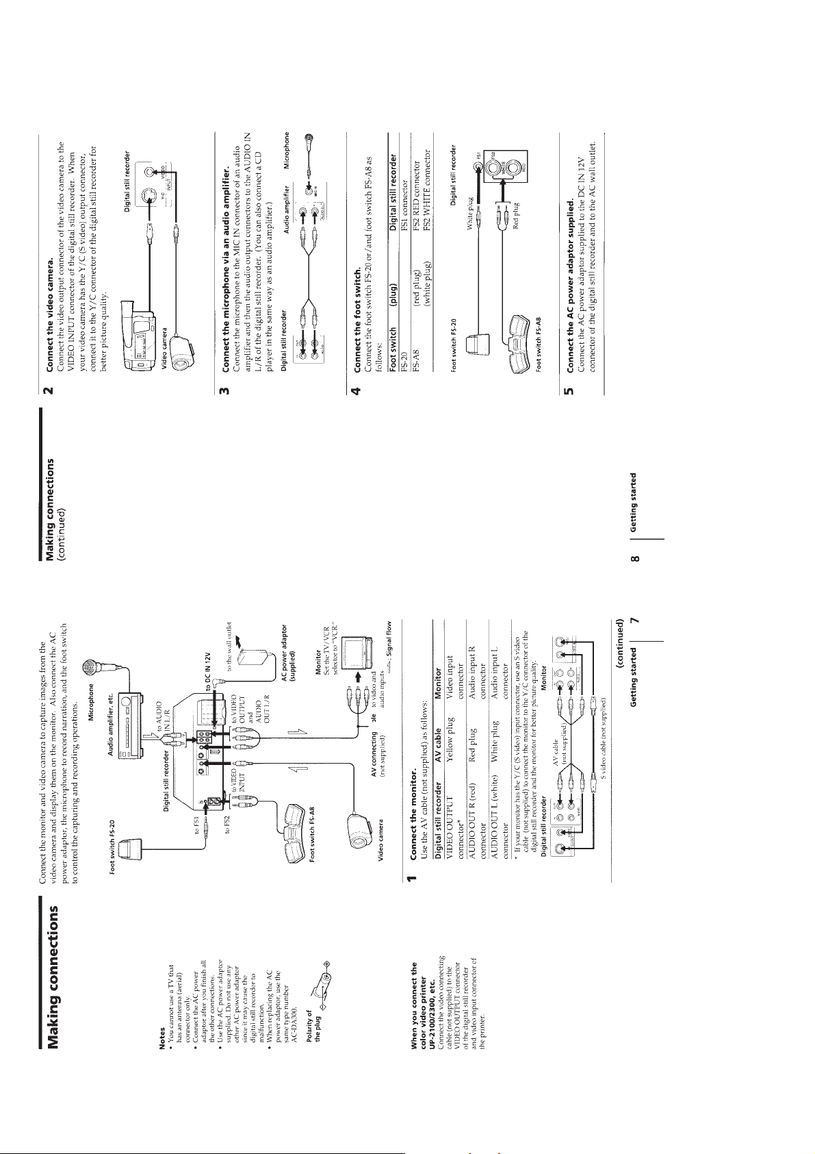
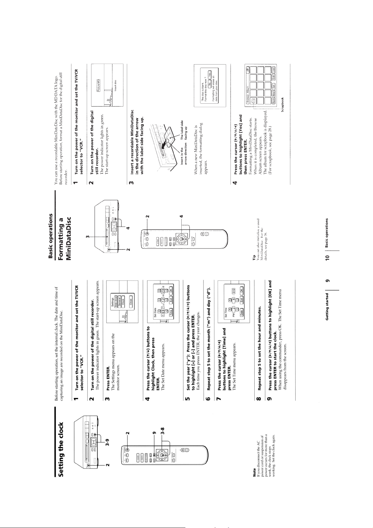
SECTION 2
GENERAL
This section is extracted
from instruction manual.
— 7 —
— 8 —
— 9 —
— 10 —
SECTION 3
)
DISASSEMBLY
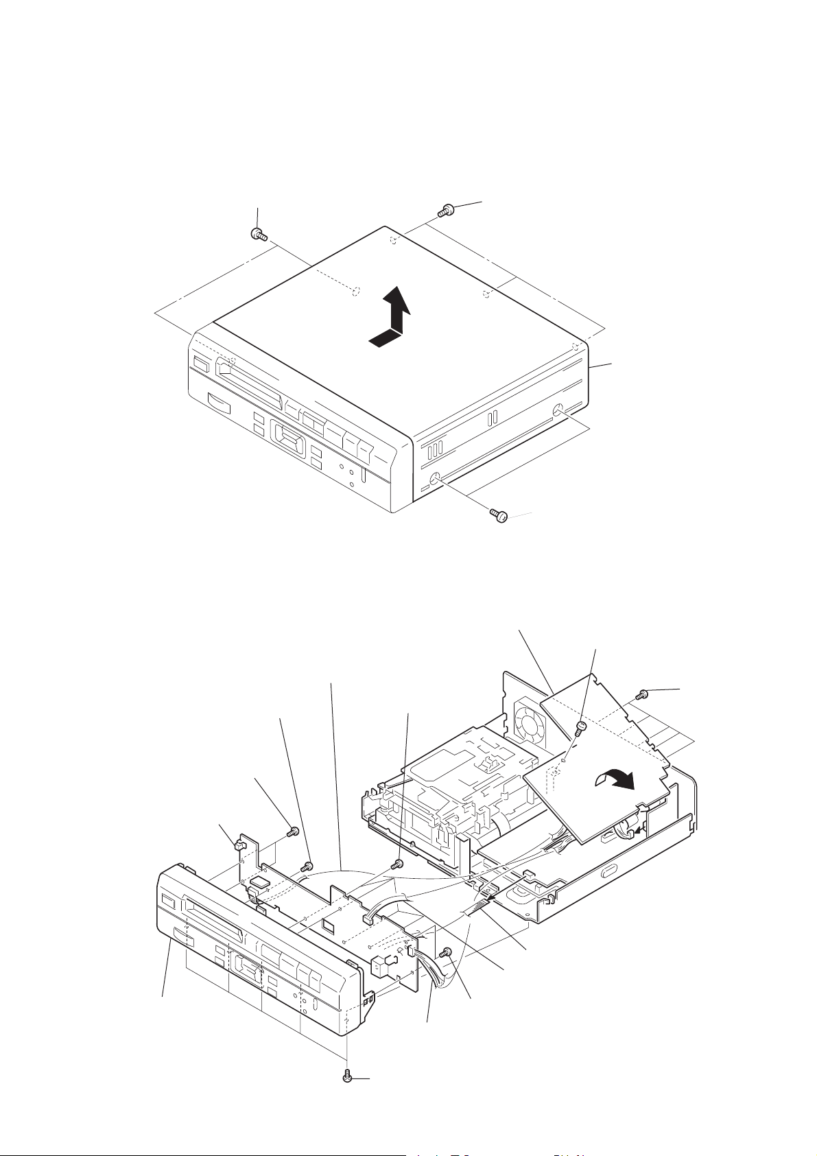
Note : Follow the disassembly procedure in the numerical order given.
3-1. UPPER CASE
1
Two screws (M3 × 8)
A
3
Two screws (BV/RING)
4
Remove the upper
case by pilling it in
the directions shown
by the arrow
A
.
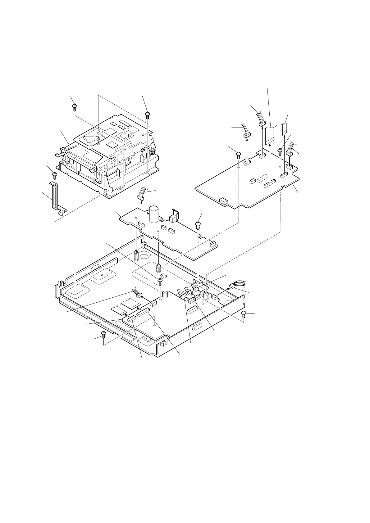
3-2. FRONT PANEL , PANEL BOARD AND VIDEO IN BOARD
4
8
Connector
(CN106 : VIDEO IN board)
!™
!¡
Screw (BVTP 2.6 × 8)
!º
Two screws
(BVTP 2.6
!¢
PANEL board
×
8)
Screw (BVTP 2.6 × 8)
2
Two screws (M3 × 8)
VIDEO IN board
3
Screw (BVTP 3 × 6)
2
Five screws
(BVTP 3
×
12
9
FRONT PANEL assy
7
Connector
(CN8201 : JACK board)
1
Five screws
(BVTP 3
×
8)
— 11 —
5
Connector (CN5003 : PICTURE board)
6
Connector (CN5002 : PICTURE board)
!£
Two screws (BVTP 2.6 × 8)
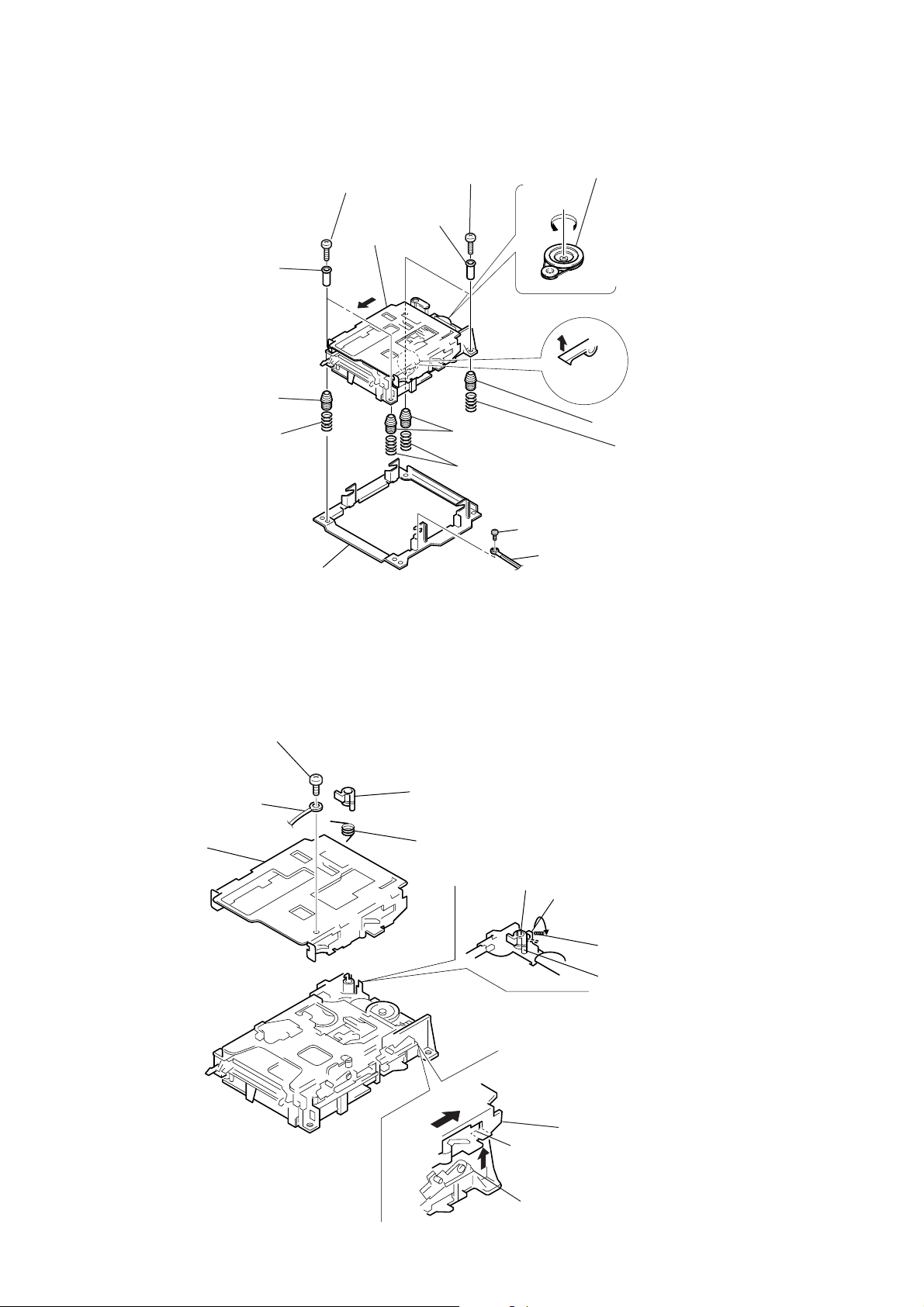
3-3. PICTURE BOARD, POWER BOARD AND MECHANISM DECK
)
@™
@£
Mechanism deck
(MDM-2BR)
!ª
Screw
(BVTP 3
@º
Stay plate
Two screws
(BVTP 3
×
6)
× 6)
!∞
@¡
Two screws (BVTP 3 × 6)
POWER board
!£
Connector
(CN1002)
5
(CN1002)
6
Screw
(BVTT 2.6
!¢
Nylon rivet
Connector
×
5)
1
(CN5001)
4
Connector
(CN1001)
Connector
2
(CN3002)
Connector
7
Screw
(BVTT 2.6
3
(CN3001)
8
PICTURE board
×
Connector
5
!§
Connector
(CN2005)
@¶
MD board
@∞
Screw (BVTP 3 × 6)
@¢
Screw
(BVTP 3
×
6)
!•
Connector (CN2001)
!º
!¡
Connector (CN2006)
!¶
Connector (CN2002)
9
Connector (CN2007)
!™
Connector (CN2501)
@§
Connector (CN2008)
Screw (BVTP 3 × 6)
— 12 —
3-4. MD MECHANISM DECK
1
(B2.6
2
Two collars
(damper)
Two screws
×
18)
Slider
B
4
(B2.6
5
Two collars
(damper)
Two screws
×
18)
Pulley (BD)
A
3
Turn the pulley (BD) in the direction
of arrow
in the direction of the arrow
(Because the slider is caught by
the stopper in the middle,
move the stopper slightly up to
make the slider free as shown in
illustration
(BD) in the direction of the arrow
A further.)
A
, and move the slider
A
. Then turn the pulley
B
.
!™
Insulator (MD)
!£
Compression coil spring
Mounting bracket (MD)
3-5. SLIDER (MD MECHANISM)
3
Screw (PTT 2 × 4)
4
Ground terminal
8
Two insulators
(MD)
9
Lever (SLM)
Illustration
Two compression coil springs
6
Screw (BVTT 2.6 × 4)
7
Ground terminal
A
!º
Insulator (MD)
!¡
Compression coil spring
Slider
Torsion coil spring
Craw B
A
B
— 13 —
Craw C
Craw D
Craw A
1
Remove the torsion coil spring
from the claw A.
2
While removing the claw B,
lift up the lever (SLM) and remove it.
5
Move the claw C of the slider
in the direction of the arrow
while taking care not to be caught
by the craw D. Lift up the claw C
of the slider.
Remove the torsion coil spring
from the claw B.
A
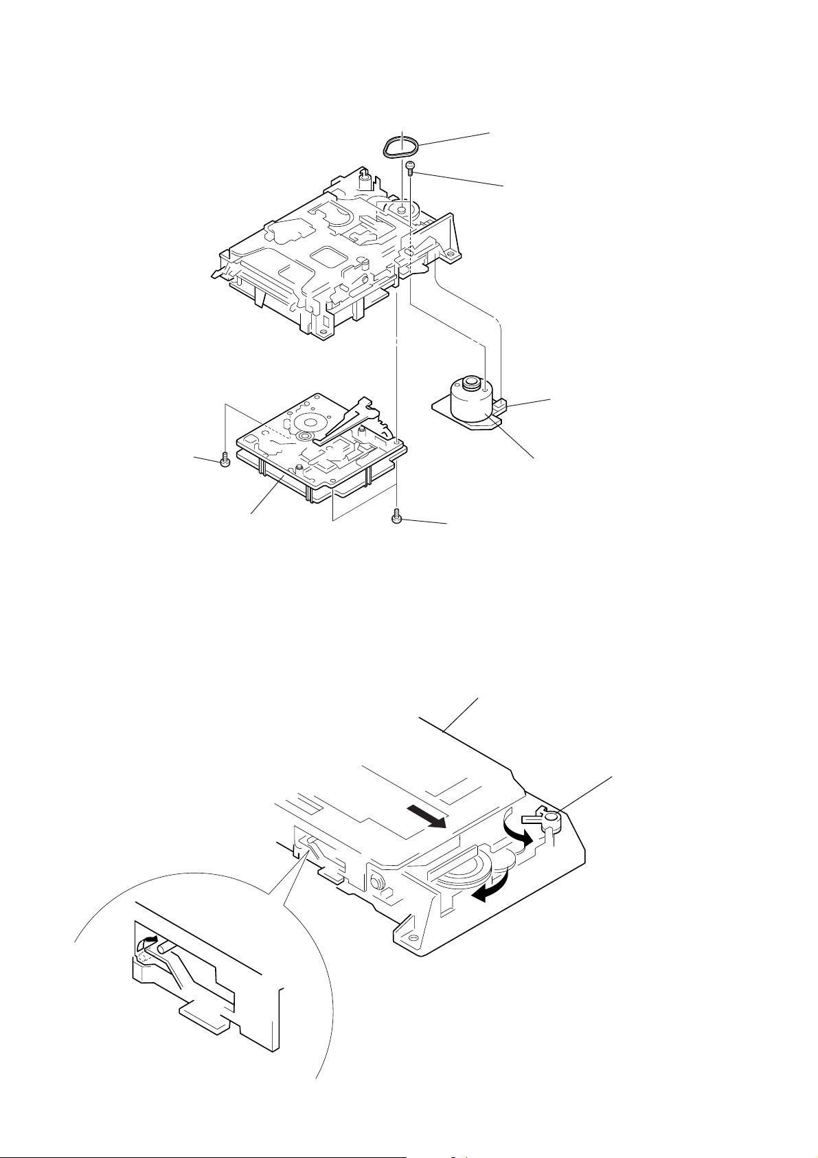
3-6. MD BASE UNIT (MBU-2) AND LOADING MOTOR ASSY
1
Screw (BVTP3 × 6)
4
Belt (BD)
5
Two screws (B2.6 × 5)
6
Connector (CN192)
7
Loading motor assy
3
MD base unit (MBU-2)
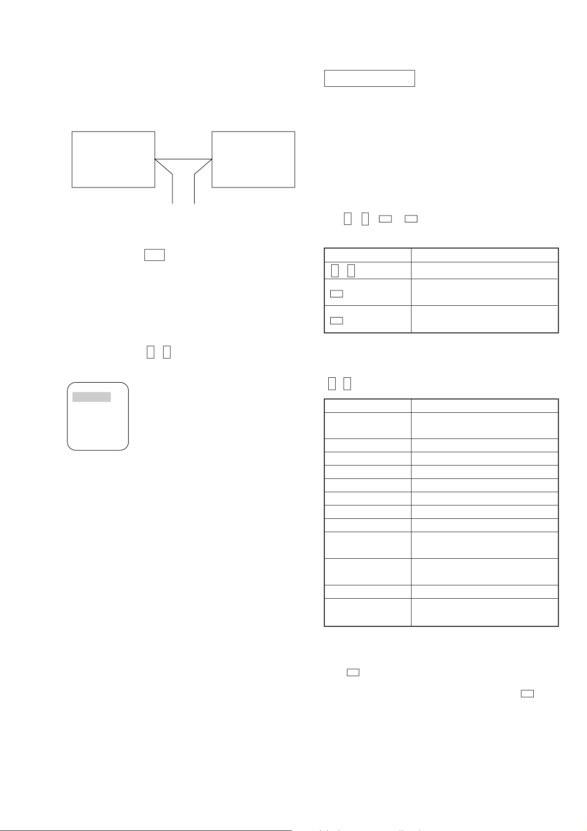
3-7. HOW TO ATTACH THE SLIDER (MD MECHANISM)
2
Two screws (BVTP3 × 6)
3
Turn the pulley (BD) in the direction
of the arrow
in the direction of the arrow
and lock it with the lever (SLM).
B
C
to move the slider
2
Turn the lever (SLM) fully
in the direction of the arrow
A
C
B
,
A
.
1
Set the four projections of the lever
in the right and the left to the position
as shown.
— 14 —
SECTION 4
TEST MODE
[PREPARATION FOR USE OF TEST MODE]
Connect the equipment as shown below before starting the test mode.
Connection:
DPA-300 Monitor
VIDEO OUTPUT connector VIDEO INPUT connector
• How to Enter the Test Mode
While pressing the + button, press the RESET button.
• How to Exit the Test Mode
Remove the AC adapter from wall outlet.
There are two test modes. One is the audio test mode and the other
is the video test mode. When the DPA-300 enters the test mode,
main menu appears allowing operator to select either audio test mode
or video test mode. Select the desired test mode by pressing the
cross marked button ( , ), and press the ENTER button.
• Main menu
Close
Audio Test
Video Test
Capture Mode
Audio Test
Refer to the respective items for more details.
Audio Test Mode → Page 15
Video Test Mode → Page 17
n
N
AUDIO SECTION
[INTRODUCTION]
Enter the test mode referring to [PREPARATION FOR USE OF
TEST MODE] in the left column of this page.
All of the messages described as “displayed” in section
“ 5. ELECTRICAL ADJUSTMENT ” appears on monitor screen
during adjustment.
1. BASIC OPERATIONS OF THE TEST MODE
All operations are performed using the cross marked button
( , , n , N ), and press the ENTER button. The
n
N
respective buttons have the following functions.
Function Name Function
, button Changes parameters and modes
n
N
n button
N button
Proceeds onto the next steps.
Confirms the entry.
Returns to the previous step.
Stop operations.
2. SELECTING THE TEST MODE
Select the desired test mode from the ten test modes by pressing the
, buttons.
n
N
Display Contents
TEMP ADJUST
LDPWR ADJUST Laser power adjustment
EFBAL ADJUST Traverse adjustment
FBIAS ADJUST Focus bias adjustment
FBIAS CHECK Focus bias check
CPLAY MODE Continuous playback mode
CREC MODE Continuous recording mode
EEP MODE Non-volatile memory mode (*1)
Vol MODE
Ver. xx.xx
Virgin mode TOC all clear mode (*1)
Total Time
Temperature compensation offset
adjustment
The mode corresponding to the
electronic volume control mode (*1)
Displays version No. of MD
microprocessor
WR = x: xx (Laser total write hours)
SP = x: xx (Spindle rotation hours)
• For detailed description of each adjustment mode, refer to the
• If a different adjustment mode has been selected by mistake, press
*1: The EEP MODE, Vol MODE, Ver.xx.xx and Virgin mode are
— 15 —
“ 5. ELECTRICAL ADJUSTMENTS ”.
the N button to exit from it.
not used in servicing. If set accidentally , press the N button
immediately to exit it.
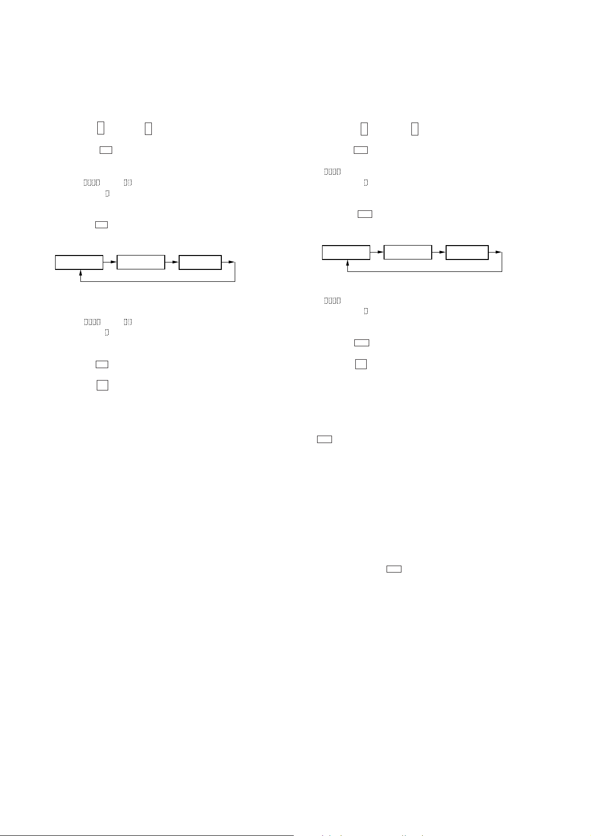
2-1. OPERA TING THE CONTINUOUS PLA YB ACK MODE
1. Entering the Continuous Playback Mode
1 Set the MO or CD disc in the unit. (Whichever recordable
discs or discs for playback only are available.)
2 Press the button or button and display “CPLAY
MODE”.
n
N
3 Press the n button to change the display to “CPLAY
IN”.
4 When access completes, the display changes to
“C1=
Note: The numbers “
”.
AD=
” displayed are undefinite numbers.
2. Changing the Parts to be Played-back
1 Press the n button during continuous playback to change
the display as below.
2-2. OPERATING THE CONTINUOUS RECORDING
MODE
1. Entering the Continuous Recording Mode
1 Set the MO disc in the unit.
2 Press the button or button and display “CREC
MODE”.
n
N
3 Press the n button to change the display to “CREC IN”.
4 When access completes, the display changes to “CREC
(
)” .
Note: The numbers “ ” displayed are undefinite numbers.
2. Changing the Parts to be Recorded
1 When the n button is pressed access is completed, the
display changes as below.
CPLAY MID
CPLAY OUT CPLAY IN
2 When access completes, the display changes to
“C1=
Note: The numbers “
AD= ”.
” displayed are undefinite numbers.
3. Exitting the Continuous Playback Mode
1 Press the N button. The display will change to “CPLA Y
MODE”.
2 Press the 6 button and remove the disc.
Notes:
1. The playback start address for IN, MID, and OUT are as follows.
IN : 40h cluster
MID : 300h cluster
OUT: 700h cluster
CREC MID
CREC OUT CREC IN
2 When access completes, the display changes to “CREC
)” .
(
Note: The numbers “
” displayed sare undefinite numbers.
3. Ending the Continuous Recording Mode
1 Press the N button. The display will change to “CREC
MODE”.
2 Press the 6 button and remove the disc.
Notes:
1. The recording start address for IN, MID, and OUT are as follows.
IN : 40h cluster
MID : 300h cluster
OUT : 700h cluster
2. The N button can be used to stop recording anytime.
3. During the test mode, the erasing-protection tab will not be
detected. Therefore be careful not to set the continuous recording
mode when a disc not to be erased is set in the unit.
4. Do not perform continuous recording for long periods of time
above 5 minutes.
5. During continuous recording, be careful not to apply vibration.
2-3. NON-VOLATILE MEMORY MODE
This mode reads and writes the contents of the non-volatile memory .
It is not used in servicing.
If set accidentally, press the N button immediately to exit it.
— 16 —
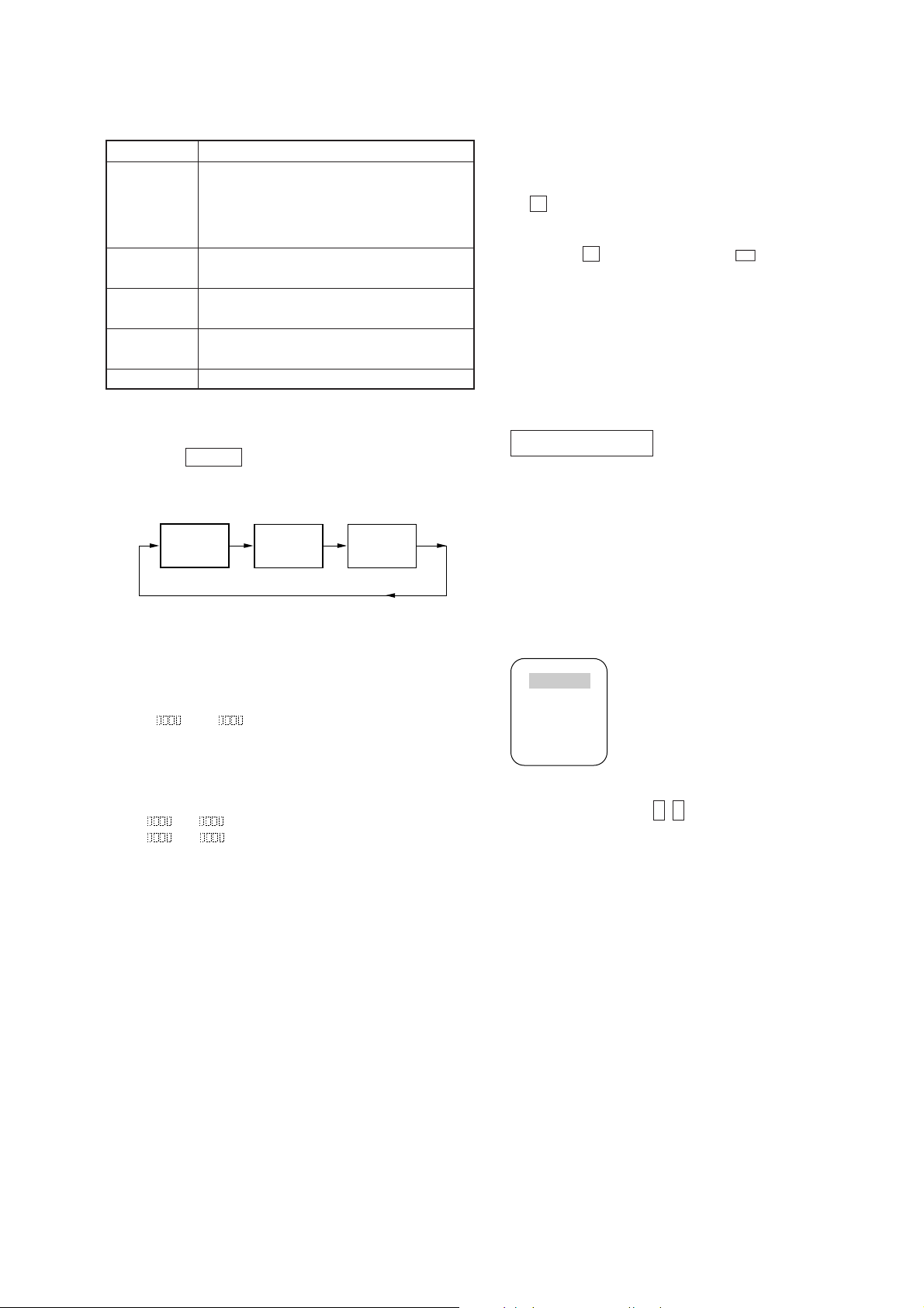
3. FUNCTIONS OF OTHER BUTTONS
5. PRECAUTIONS FOR USE OF TEST MODE
Button Function
• Sets continuous playback when
LIVE/PLAY
pressed in the STOP state.
• When pressed during continuous
playback, the tracking servo turns on/off.
CAPTURE
PHOTO
ALBUM
IR LINK
Stop continuous playback and continuous
recording.
The sled moves to the outer circumference only
when this is pressed.
The sled moves to the inner circumference only
when this is pressed.
Switches the diaplay when pressed.
4. TEST MODE DISPLAYS
Each time the IR LINK button pressed, the display changes in the
following order.
Mode
display
Error rate
display
Address
Display
1. As loading related operations will be performed regardless of
the test mode operations being performed, be sure to check that
the disc is stopped before setting and removing it. Even if the
6 button is pressed while the disc is rotating during continuous
playback, continuous recording, etc., the disc will not stop
rotating. Therefore, it will be ejected while rotating. Be sure to
press the 6 button after pressing the N button and the rotation
of disc is stopped.
2. The erasing-protection tab is not detected in the test mode.
Therefore, operating in the recording laser emission modes
suchas continuous resord mode, traverse adjustment mode, etc.,
the recorded contents will be erased regardless of the position
of the tab. When using a disc that is not to be erased in the test
mode, be careful not to enter the continuous recording mode
and traverse adjustment mode.
VIDEO SECTION
[INTRODUCTION]
Enter the test mode referring to [PREPARATION FOR USE OF
TEST MODE] on page 15.
• VIDEO TEST MODE
Enter the video test mode by selecting VIDEO on the main menu.
The various video test signals are output from built-in
microprocessor in the video test mode.
1. MODE display
Displays “TEMP ADJUST”, “CPLAY MODE”, etc..
2. Error rate display
Error rates are displayed as follows.
C1=
AD=
C1= : Indicates C1 error
AD= : Indicates ADER
3. Address display
Address are displayed as follows.
h= s= (MO pits and CD)
h=
a= (MO grooves)
h= : Header address
a= : ADIP address
s= : SUB Q address
Note: “—” is displayed when the address cannot be read.
• Menu
Close
Color Bar
Blue Back
Half Tone
White
The menu as shown appears. Select the desired submenu by pressing
the cross marked button ( , ), and press the ENTER button.
n
N
Color Bar ............ The color bars signal is output.
Blue Back ........... All blue screen appears.
Half Tone ............ All gray screen appears.
White .................. 100% white signal is output.
• When a desired submenu is selected, the specified screen appears,
but the submenu remains on the display.
Press “Close” to clear the submenu. The submenu disappears
and the specified screen appears.
Return to the main menu of the test mode by pressing the ENTER
button.
— 17 —
SECTION 5
ELECTRICAL ADJUSTMENTS
AUDIO SECTION
[INTRODUCTION]
Enter the test mode referring to [PREPARATION FOR USE OF
TEST MODE] on page 15.
All of the messages described as “displayed” appears on monitor
screen during adjustment.
Precautions for Checking Laser Diode Emission
To check the emission of the laser diode during adjustments, never
view directly from the top as this may lose your eye-sight.
Precautions for Use of optical pick-up (KMS-210A)
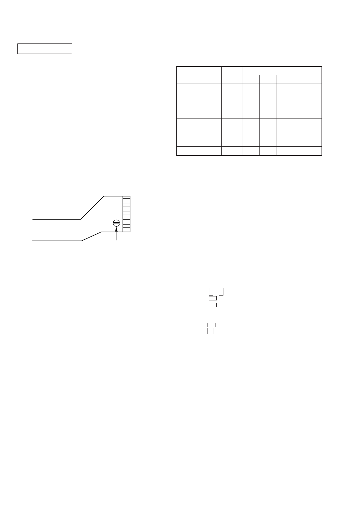
As the laser diode in the optical pick-up is easily damaged by static
electricity, solder the laser tap of the flexible board when using it.
Before disconnecting the connector, desolder first. Before connecting
the connector, be careful not to remove the solder . Also take adequate
measures to prevent damage by static electricity . Handle the flexible
board with care as it breaks easily.
laser tap
Precautions for Adjustments
1) When replacing the following parts, perform the adjustments
and checks with ® in the order shown in the following table.
Optical
Pick-up
1. Temperature
compensation
offset adjustment
2. Laser power
adjustment
3. Traverse
adjustment
4. Focus bias
adjustment
5. Error rate check
IC171
G
¬¬
¬
¬¬ ¬
¬
GG
¬
¬¬
2) Set the test mode when performing adjustments.
After completing the adjustments, exit the test mode.
3) Perform the adjustments in the order shown.
4) Use the following tools and measuring devices.
• Check Disc (CD) TGYS-1 (Parts No. 4-963-646-01)
• Laser power meter LPM-8001 (Parts No. J-2501-046-A)
• Oscilloscope
• Digital voltmeter
• Thermometer
5) When observing several signals on the oscilloscope, etc.,
make sure that VC and ground do not connect inside the
oscilloscope.
(VC and ground will become short-circuited.)
BD Board
D101 IC101, IC121, IC191
¬¬¬
G
G
G
¬
Optical pick-up flexible board
• Abbreviation
MO : Recordable disc
CD : Disc for playback only
Creating Continuously Recorded Disc
* This disc is used in focus bias adjustment and error rate check.
The following describes how to create a continuous recording
disc.
1. Insert a MO disc (blank disc) commercially available.
2. Press the , buttons and display “CREC MODE”.
3. Press the n button and display “CREC IN”.
n
N
4. Press the n button again to display “CREC MID”.
“CREC (0300” is displayed for a moment and recording starts.
5. Complete recording within 5 minutes.
6. Press the N button and stop recording .
7. Press the § button and remove the MO disc.
The above has been how to create a continuous recording data for
the focus bias adjustment and error rate check.
Note :
• Be careful not to apply vibration during continuous recording.
— 18 —
Temperature Compensation Offset Adjustment
Laser Power Adjustment
Save the temperature data at that time in the non-volatile memory
as 25 ˚C reference data.
Note :
1. Usually, do not perform this adjustment.
2. Perform this adjustment in an ambient temperature of 22 ˚C to
28 ˚C. Perform it immediately after the power is turned on
when the internal temperature of the unit is the same as the
ambient temperature.
3. When D101 has been replaced, perform this adjustment after
the temperature of this part has become the ambient
temperature.
Adjusting Method :
1. Press the , buttons and display “TEMP ADJUST”.
n
N
2. Press the n button and select the “TEMP ADJUST” mode.
3. “TEMP =
” and the current temperature data will be
displayed.
4. To save the data, press the n button.
When not saving the data, press the N button.
5. When the n button is pressed, “TEMP =
SAVE” will be
displayed for some time, followed by “TEMP ADJUST”.
When the N button is pressed, “TEMP ADJUST” will be
displayed.
Specifications :
The “TEMP =
” should be within “E0 - EF”, “F0 - FF”, “00 -
0F”, “10 - 1F” and “20 - 2F”.
Connection :
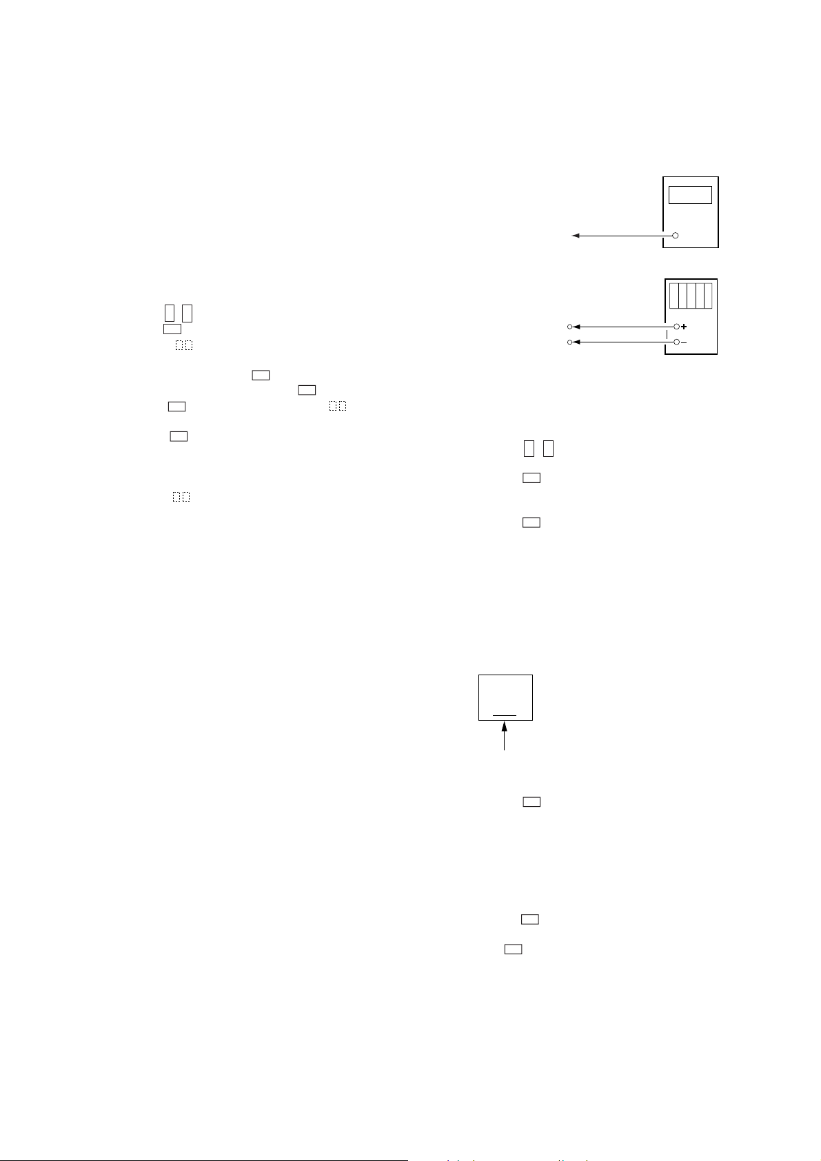
Laser power
meter
Optical pick-up
objective lens
Digital voltmeter
BD board
TP (I + 5V)
TP (IOP)
Adjusting Method :
1. Set the laser power meter on the objective lens of the optical
pick-up. (When it cannot be set properly, press the ALBUM
button or PHOTO button and move the optical pick-up.)
Connect the digital volt meter to TP (IOP) and TP (I+5V).
2. Press the , buttons and display “LDPWR ADJUST”.
(Laser power : For adjustment)
n
N
3. Press the n button twice and display “LD $ 4B = 3.5 mW”.
4. Adjust RV102 of the BD board so that the reading of the laser
power meter becomes 3.45
+0.1
– 0
mW.
5. Press the n button and display “LD $ 96 = 7.0 mW”.
(Laser power : MO writing)
6. Check that the laser power meter and digital voltmeter readings
satisfy the specified value.
Specification :
Laser power meter reading : 7.0 ± 0.3 mW
Digital voltmeter reading : Optical pick-up displayed value ± 10%
(Optical pick-up label)
KMS
210A
27X40
B0825
lop = 82.5 mA in this case
lop (mA) = Digital voltmeter reading (mV)/ 1 (
Ω
)
7. Press the n button and display “LD $ 0F = 0.7 mW”.
(Laser power : MO reading)
8. Check that the laser power meter at this time satisfies the
specified value.
Specification :
Laser power meter reading : 0.70 ± 0.1 mW
9. Press the N button and display “LDPWR ADJUST”, and stop
laser emission.
(The N button is effective at all times to stop the laser
emission.)
— 19 —
Traverse Adjustment
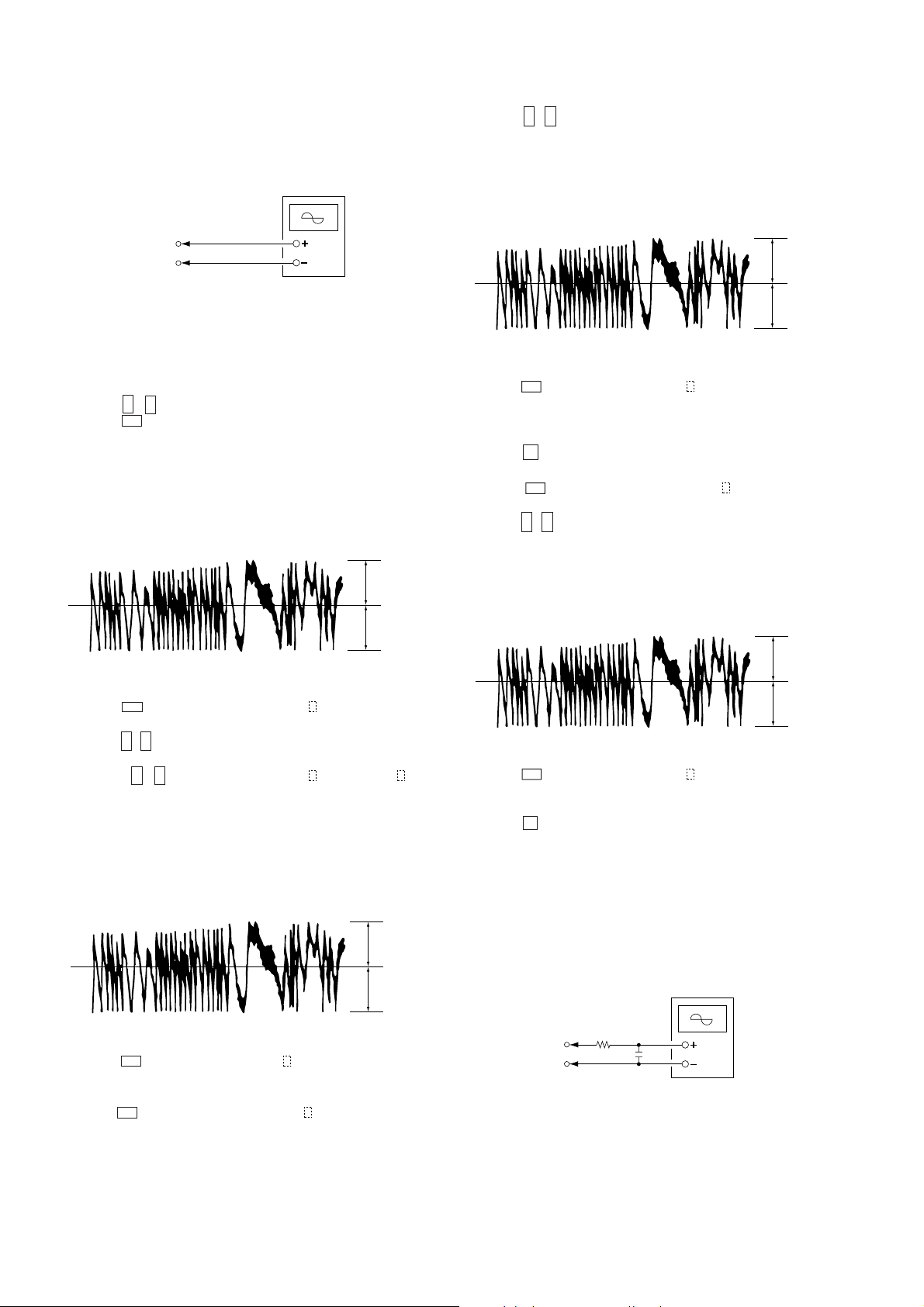
Connection :
Oscilloscope
11. Press the , buttons until the waveform of the oscilloscope
n
N
moves closer to the specified value.
In this adjustment, waveform varies at intervals of approx. 3%.
Adjust the waveform so that the specified value is satisfied as
much as possible.
BD board
TP (TEO)
TP (VC)
Adjusting method :
1. Connect an oscilloscope to TP (TEO) and TP (VC) of the BD
board.
2. Load a MO disc (any available on the market).
3. Press the ALBUM button or PHOTO button and move the
optical pick-up outside the pit.
4. Press the , buttons and display “EFBAL ADJUST”.
5. Press the n button and display “EFBAL MO-W”.
n
N
(Laser power WRITE power/Focus servo ON/tracking servo
OFF/spindle (S) servo ON)
6. Adjust RV101 of the BD board so that the waveform of the
oscilloscope becomes the specified value.
(MO groove write power traverse adjustment)
(Traverse Waveform)
A
VC
B
Specification A = B
7. Press the n button and display “EFB = $
MO-R”.
(Laser power : MO reading)
8. Press the , buttons so that the waveform of the oscilloscope
becomes the specified value.
(When the , buttons are pressed, the
changes and the waveform changes.) In this adjustment,
n
n
N
N
of “EFB = $ ”
waveform varies at intervals of approx. 3%. Adjust the
waveform so that the specified value is satisfied as much as
possible.
(MO groove read power traverse adjustment)
(Traverse Waveform)
A
VC
B
(Traverse Waveform)
A
VC
B
Specification A=B
12. Press the n button, display “EFB = $ SA VE” for a moment
and save the adjustment results in the non-volatile memory.
Next “EFBAL CD” is displayed. The disc stops rotating
automatically.
13. Press the § button and remove the MO disc.
14. Load the check disc (MD) TDYS-1.
15. Press the n button and display “EFB = $
CD”. Servo is
imposed automatically.
16. Press the , buttons so that the waveform of the oscilloscope
moves closer to the specified value.
n
N
In this adjustment, waveform varies at intervals of approx. 3%.
Adjust the waveform so that the specified value is satisfied as
much as possible.
(Traverse Waveform)
A
VC
B
Specification A=B
17. Press the n button, display “EFB = $ SA VE” for a moment
and save the adjustment results in the non-volatile memory.
Next “EFBAL ADJUST” is displayed.
18. Press the § button and remove the test disc TDYS-1.
Note 1 : Data will be erased during MO reading if a recorded disc
is used in this adjustment.
Note 2 : If the traverse waveform is not clear, connect the
oscilloscope as shown in the following figure so that it
can be seen more clearly.
Oscilloscope
Specification A=B
9. Press the n button, display “EFB = $
SAVE” for a moment
and save the adjustment results in the non-volatile memory.
Next “EFBAL MO-P” is displayed.
10. Press the n button and display “EFB = $
MO-P”.
The optical pick-up moves to the pit area automatically and
servo is imposed.
— 20 —
BD board
TP (TEO)
TP (VC)
330k
Ω
10pF
DPA-300
Focus Bias Adjustment
Adjusting Method :
1. Load a continuously recorded disc (Refer to “Page 18 Creating
Continuously Recorded Disc”.).
2. Press the , buttons and display “CPLAY MODE”.
3. Press the n button twice and display “CPLAY MID”.
4. Press the N button when “C1 =
5. Press the , buttons and display “FBIAS ADJUST”.
6. Press the n button and display “ / a = ”.
The first four digits indicate the C1 error rate, the two digits
after [/] indicate ADER, and the 2 digits after [a =] indicate the
focus bias value.
7. Press the , buttons and find the focus bias value at which
the C1 error rate becomes 220.
8. Press the n button and display “
9. Press the , buttons and find the focus bias value at which
the C1 error rate becomes 220.
10. Press the n button and display “
11. Check that the C1 error rate is below 50 and ADER is 00. Then
press the n button.
12. If the “(
button.
If below 20, press the N button and repeat the adjustment
from step 2 again.
13. Press the § button to remove the continuously recorded disc.
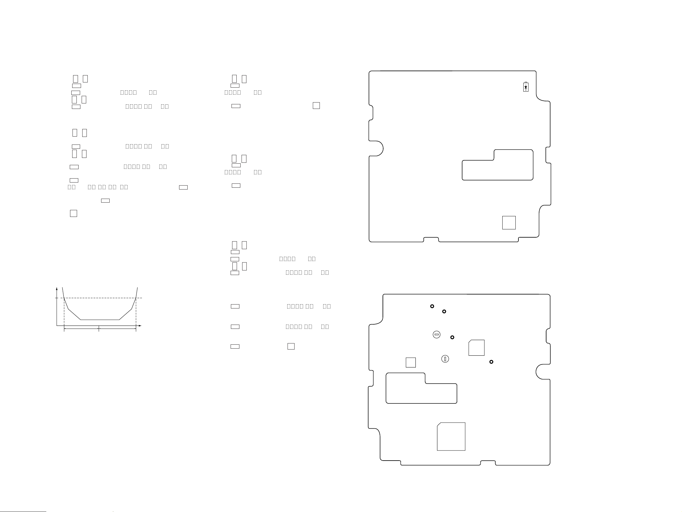
Note 1 : The relation between the C1 error and focus bias is as
Note 2 : As the C1 error rate changes, perform the adjustment using
C1 error
220
n
N
AD = ” is displayed.
n
N
n
N
/ b = ”.
n
N
/ c = ”.
” in “ - - ( ” is above 20, press the n
shown in the following figure. Find points a and b in the
following figure using the above adjustment. The focal
point position c is automatically calculated from points a
and b.
the average value.
Focus bias value
(F. BIAS)
b
c
a
Error Rate Check
CD Error Rate Check
Checking Method :
1. Load a check disc TGYS-1.
2. Press the , buttons and display “CPLAY MODE”.
3. Press the n button twice and display “CPLAY MID”.
4. “C1 =
n
N
AD = ” is displayed.
5. Check that the C1 error rate is below 20.
6. Press the N button, stop playback, press the § button, and
remove the test disc.
MO Error Rate Check
Checking Method :
1. Load a continuously recorded disc (Refer to “Page 18 Creating
Continuously Recorded Disc”.).
2. Press the , buttons and display “CPLAY MODE”.
3. Press the n button twice and display “CPLAY MID”.
n
N
4. “C1 = AD = ” is displayed.
5. If the C1 error rate is below 50, check that ADER is 00.
6. Press the N button, stop playback, press the § button, and
remove the continuously recorded disc.
Focus Bias Check
Change the focus bias and check the focus tolerance amount.
Checking Method :
1. Load a continuously recorded disc (Refer to “Page 18 Creating
Continuously Recorded Disc”.).
2. Press the , buttons and display “CPLAY MODE”.
3. Press the n button twice and display “CPLAY MID”.
4. Press the N button when “C1 =
5. Press the , buttons and display “FBIAS CHECK”.
6. Press the n button and display “ / c = ”.
The first four digits indicate the C1 error rate, the two digits
after [/] indicate ADER, and the 2 digits after [c =] indicate the
focus bias value.
Check that the C1 error is below 50 and ADER is 00.
7. Press the n button and display “
Check that the C1 error is not below 220 and ADER is not
above 00 every time.
8. Press the n button and display “
Check that the C1 error is not below 220 and ADER is not
above 00 every time.
9. Press the N button, next press the § button, and remove the
continuously recorded disc.
n
n
N
AD = ” is displayed.
N
/ b = ”.
/ a = ”.
Adjusting Points and Connecting Points
[BD BOARD] (SIDE A)
[BD BOARD] (SIDE B)
(IOP)
(I + 5V)
IC171
(VC)
RV101
TRAVERSE
Adj
IC101
D101
IC191
Note 1 : If the C1 error and ADER are above 00 at points a or b,
the focus bias adjustment may not have been carried out
properly. Adjust perform the beginning again.
RV102
LASER POWER
Adj
IC121
(TEO)
— 21 — — 22 —
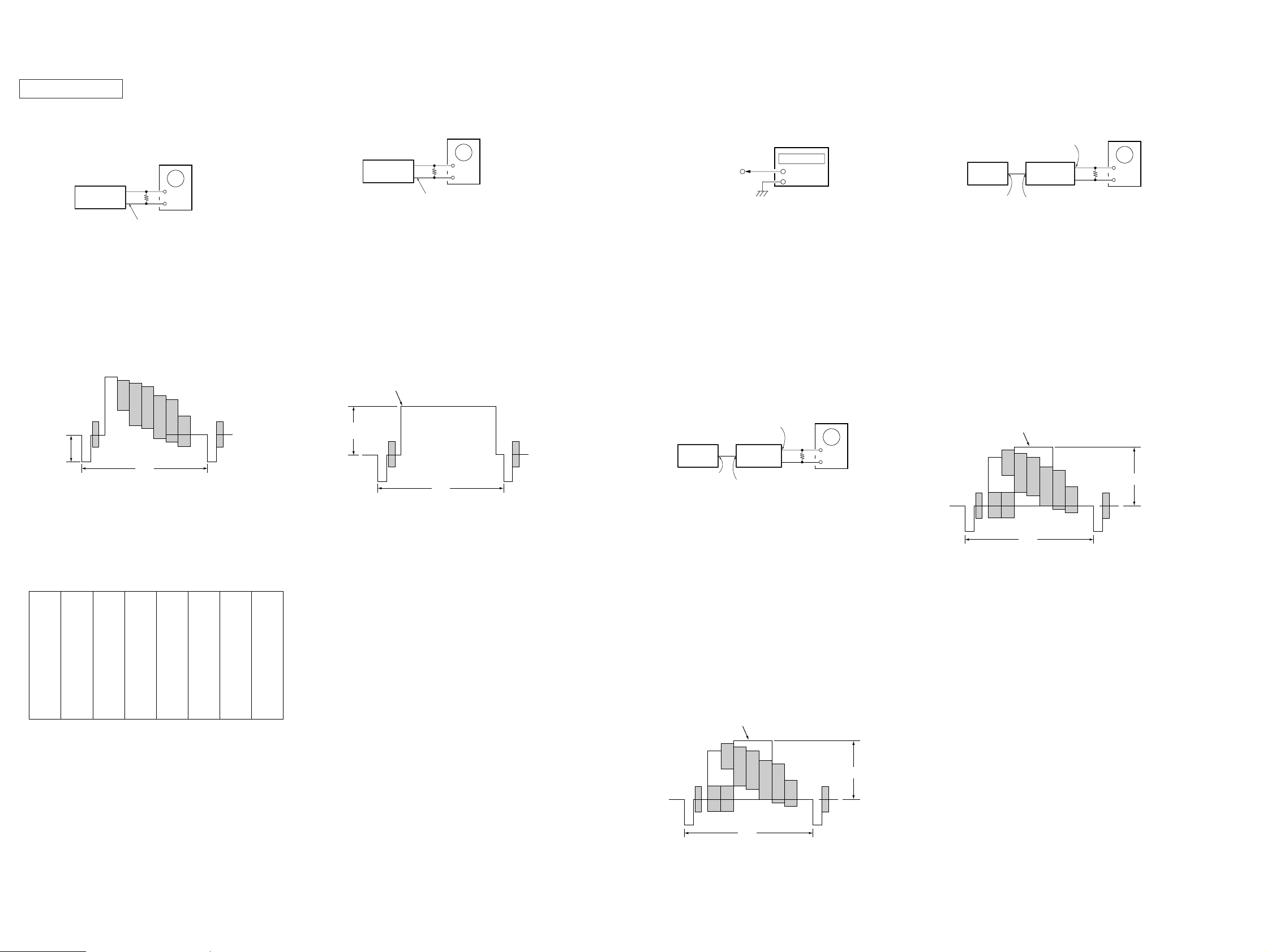
DPA-300
r
+
–
75
Ω
DPA-300
Oscilloscope
Video Output (J106)
Color bar generator
S-Video Input
(J101)
Video Output
A
H
White (100 %)
VIDEO SECTION
[SYNC LEVEL ADJUSTMENT]
Connection:
Oscilloscope
75
Ω
DPA-300
Video Output (J106)
Adjustment Procedure:
1. Connect an oscilloscope and monitor to the Video Output (J106)
of the DPA-300.
2. Enter the video test mode. Output the color bar from the DP A-
300. (Refer to page 15.) After color bar output is confirmed,
disconnect a monitor.
3. Adjust RV3003 on the PICTURE board until the level (A)
satisfies the specification on an oscilloscope.
Waveform:
+
–
[WHITE LEVEL ADJUSTMENT]
Connection:
Oscilloscope
75
Ω
DPA-300
Video Output (J106)
+
–
Adjustment Procedure:
1. Connect an oscilloscope and monitor to the Video Output (J106)
of the DPA-300.
2. Enter the video test mode. Output the 100 % white signal from
the DP A-300. (Refer to page 15.) After the 100 % white signal
is confirmed, disconnect a monitor.
3. Observe waveform on an oscilloscope. Adjust RV3001 on the
PICTURE board until the level (A) of the color bar’s white
peak (100 %) satisfies the specification on an oscilloscope.
Waveform:
White (100 %)
[CLOCK ADJUSTMENT]
Connection:
Frequency counte
PICTURE board
TP4091 (DCLK)
+
–
Adjustment Procedure:
1. Connect a frequency counter to TP4091 (DCLK) on the
PICTURE board.
2. Turn the POWER switch of the DPA-300 to ON.
3. Adjust CT4001 on the PICTURE board until frequency of
TP4091 (DCLK) satisfies the specification.
Specification: 12.272725 MHz ± 30 Hz
Adjustment Location: PICTURE board
[ S INPUT Y-SIGNAL AMPLITUDE ADJUSTMENT]
Connection:
[Y OUTPUT AMPLITUDE ADJUSTMENT]
Connection:
Video Output (J106)
Color bar generator
Video Output
DPA-300
S-Video Input
(J102)
Oscilloscope
75
Ω
+
–
Adjustment Procedure:
1. Connect a color bar generator to the Video input (J102) of the
DPA-300.
2. Connect an oscilloscope and monitor to Video Output (J106) of
the DPA-300.
3. Output the 100 % white color bar signal from a color bar
generator.
4. Set the mode in which the Through picture is displayed. (Refer
to SERVICE NOTE on page 5.) After the mode is set, disconnect
a monitor.
5. Adjust RV402 of the VIDEO-IN board until the 100 % white
level (A) satisfies the specification on an oscilloscope.
Waveform:
A
H
Specification: 286 ± 15 mVp-p
(Measured in the 50 mV range of oscilloscope)
Adjustment Location: PICTURE board
- Reference -
Pattern of built-in color bar signal
CYAN
YELLOW
WHITE (100%)
GREEN
MAGENTA
RED
BLUE
BLACK
A
H
Specification: 714 ± 30 mVp-p
(Measured in the 100 mV range of oscilloscope)
Adjustment Location: PICTURE board
Adjustment Procedure:
1. Connect a color bar generator to the S-Video input (J101) of the
DPA-300.
2. Connect an oscilloscope and monitor to Video Output (J106) of
the DPA-300.
3. Output the 100 % white color bar signal from a color bar
generator.
4. Set the mode in which the Through picture is displayed. (Refer
to SERVICE NOTE on page 5.) After the mode is set, disconnect
a monitor.
5. Adjust RV403 of the VIDEO-IN board until the 100 % white
level (A) satisfies the specification on an oscilloscope.
Waveform:
White (100 %)
Specification: 714 ± 30 mVp-p
Adjustment Location: VIDEO-IN board
A
H
Specification: 714 ± 30 mVp-p
Adjustment Location: VIDEO-IN board
— 23 — — 24 —
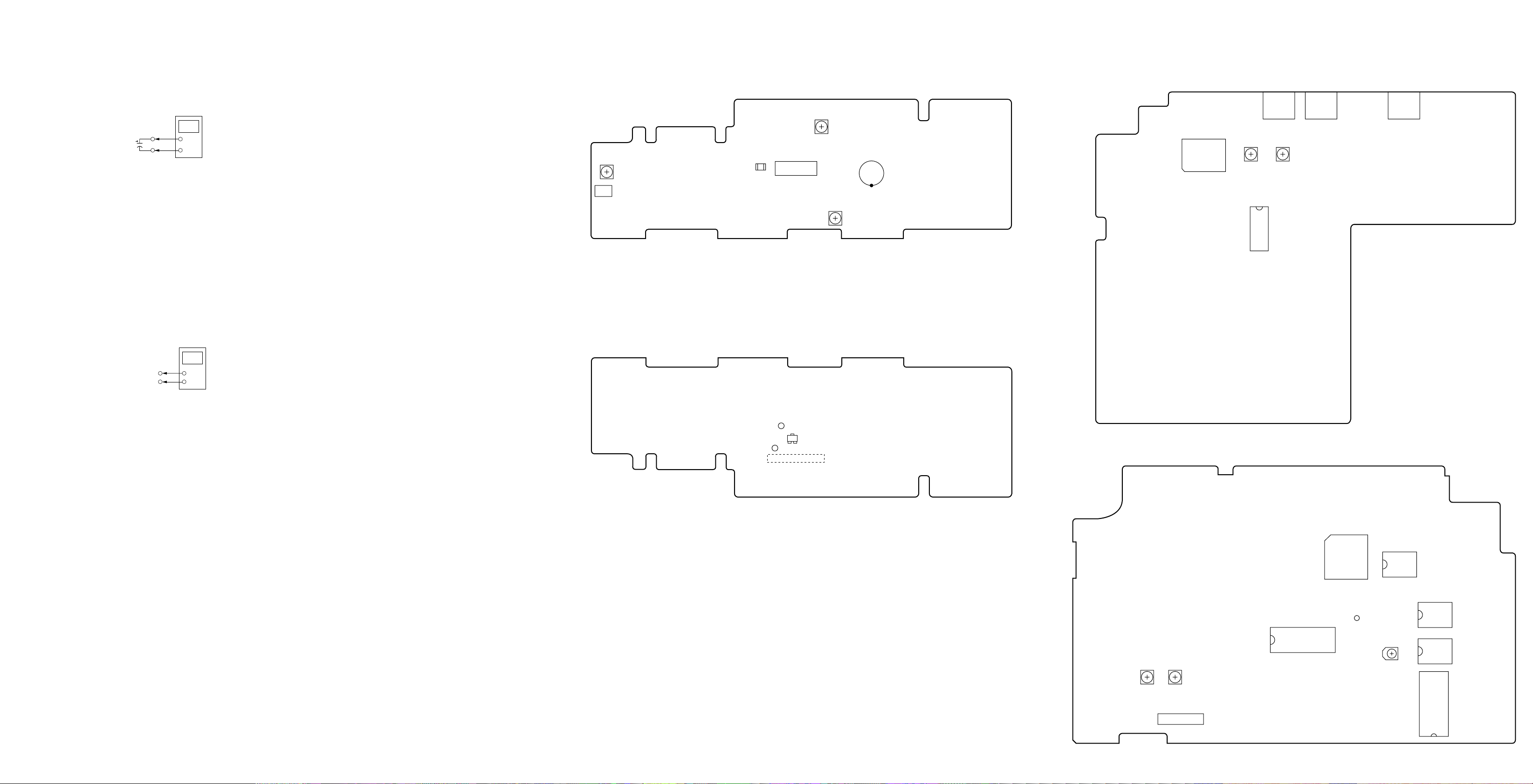
DPA-300
r
[+6 V ADJUSTMENT]
Connection:
Digital Voltmeter
POWER board
C1204
C1501
+
–
Adjustment Procedure:
1. Connect a digital voltmeter across C1204 of the POWER board.
2. Adjust RV1 1 11 on the POWER board until the digital voltmeter
reading satisfies the specification.
3. Connect a digital voltmeter across C1501 of the POWER board.
4. Adjust RV1201 on the POWER board until the digital voltmeter
reading satisfies the specification.
Specification: 6.0 ± 0.1 V
Adjustment Location: POWER board
[+5.3 V ADJUSTMENT]
Connection:
Digital Voltmete
Adjusting Points and Connecting Points
[POWER BOARD] (SIDE A)
RV1111
+6V Adj
CN1901
[POWER BOARD] (SIDE B)
C1204
+6V Adj
CN1004
RV1121
+5.3V Adj
RV1201
+6V Adj
C1501
+6V Adj
[VIDEO-IN BOARD] (SIDE A)
IC401
J101 J102 J106
RV402
Y OUTPUT
AMPLITUDE
Adj
IC402
RV403
S INPUT
SIGNAL AMPLITUDE
Adj
POWER board
TP (M+5V)
TP (MGND)
+
–
Adjustment Procedure:
1. Connect a digital voltmeter to TP (M+5 V) and TP (MGND) of
the POWER board.
2. Adjust RV1 121 on the POWER board until the digital voltmeter
reading satisfies the specification.
Specification: 5.3 ± 0.1 V
Adjustment Location: POWER board
MGND
+5.3V Adj
M+5V
+5.3V Adj
IC1121
Q1001
[PICTURE BOARD] (SIDE A)
IC4004
TP4091
(DCLK)
IC4019
IC4010
IC1003
IC4011
RV3003
SYNC
LEVEL
Adj
RV3001
WHITE
LEVEL
Adj
CN1002
CT4001
CLOCK
Adj
IC4016
— 25 — — 26 — — 27 —
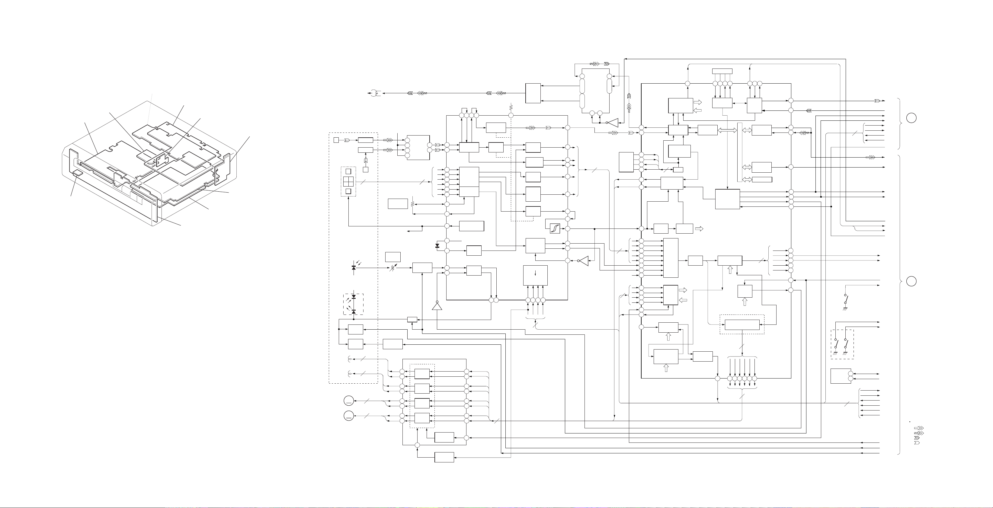
DPA-300
d
SECTION 6
DIAGRAMS
6-1. CIRCUIT BOARD LOCATION 6-2. BLOCK DIAGRAM — BD SECTION —
BD board
IRDA board
MOTOR board
POWER board
VIDEO IN board
DETECTION SW board
MD board
PANEL board
JACK board
PICTURE boar
HR901
OVER
WRITE
HEAD
OPTICAL PICK–UP BLOCK
(KMS–210A/J–N)
J
F
CDB
A
E
PD
HIGH
POWER
LD
L.F
MOD
H.F
MOD
TRACKING
COIL
FOCUS
COIL
M101
SLED
M
MOTOR
M102
MOTOR
16
M
SPINDLE
IV–AMP
IV–AMP
1
6
2
2
2
2
RV101
BALANCE
RV102
LASER
POWER
Q164
HF
MODULE
SWITCH
TRK–
TRK+
FCS+
FCS–
SLED+
SLED–
SPDL+
SPDL–
VC
E–F
IC172
2
3
BUFFER
6
5
VC
VC
Q101
LASER ON
SWITCH
Q162,163
APC
SLED/SPINDLE MOTOR DRIVE,
FOCUS/TRACKING COIL DRIVE
26
DRIVER
29
8
DRIVER
11
15
DRIVER
13
22
DRIVER
24
33
DIGITAL SIGNAL PROCESSOR.
DIGITAL SERVO SIGNAL PROCESSOR.
EFM/ACIRC ENCODER/DECODER
2
FILTER
SPFD
SPRD
5
VC
4
IC121
EFMO
45
58
CLTV
60
FILI
62
PCO
61
FILO
63
94
93
82
AUX
68
BOTM
65
PEAK
64
ABCD
66
FE
67
TE
77
SE
76
VC
69
SWDT
8
SCLK
9
XLAT
10
XRST
16
REC
24
SRDT
DIRC
7
RFI
PROCESSOR
ADIP
DEMOD
SERVO
CONTROL
SERVO
AUTO
SEQUENCER
SUBCODE
PROCESSOR.
READER/
GENERATOR
MOD/DMOD
TIMING
GENERATOR
4
DIGITAL
CLV
ANALOG
MUX
CPU
IF
EFM
EFM
PLL
ADIP
DECODER
14
SOSY
A/D
CONV
CONTROL
SENS
41
34
38
39
37
35
30
31
ADFG
33
26
29
4
27
18 2
11
|
OVER WRITE
HEAD DRIVE
14
IC181
15
|
17
1 19
5
2
IC102
4
IC182
3
|
9
Q181,182
HEAD
+5V
46 45 44 43 42
RF AGC
&EQ
J
48
1
47
7
6
4
2
IC151
CLOCK
DETECTOR
RESET
SWITCH
16
12
10
11
IC122
Q151
D101
2
3
4
5
6
7
8
9
1
I
A
B
C
D
E
F
FI
FO
VC
TEMPR
TEMPI
PD
APCREF
RF AMP
IV AMP
IV AMP
+2.5V
GENERATOR
+5V
TEMP
AMP
APC
TFDR
31
TRDR
32
FRDR
5
FFDR
6
SFDR
17
SRDR
18
SPFD
19
SPRD
20
FS4
3
BPF
AAPC
DAPC
8
DRIVE
AUX
SW
PEAK &
BOTTOM
ABCD
AMP
FOCUS
ERROR
AMP
AT
AMP
TRACKING
ERROR
AMP
SERIAL
PARALLEL
DECODER
SCLK
XRST
SWDT
17 1814 15 19 20
4
RF
AUX
BOTM
PEAK
ABCD
FE
ADFM
ADIN
TE
SE
TLB
XLAT
REGISTER
FILTER
51
52
49
53
DIFI
DICV
DIPD
DIFO
DIN
PLL
TIMING
GENERATOR
&
CLOCK
GENERATOR
PROCESSOR
SERVO DSP/PWM GENERATOR
FOCUS/TRACKING/
SLED SERVO & PWM
TRDR
SENS
12
TFDR
86851187
APC
PWM
GEN
FFDR
FRDR
899192
15
DIGITAL
6
SRDR
6
DQSY
AUDIO
IN/OUT
21
20
DIN
DOUT
AUDIO
DATA
CONTROL
ECC
ENCODER
DECODER
32K RAM
5
SFDR
DIDT
DODT
DFCT
SHCK
OFTRK
COUT
DTO
DTI
C2PO
BCK
LRCK
FS4
XTAI
FOK
WRPWR
LDDRLD
28
27
30
29
31
32
33
90
35
3
2
4
98
99
6
84
–1 –2
IC171
MEMORY
SDA
SCL
S101
LIMIT
5
6
6
4
S102–1
PROTECT
S102–2
REFLECT
DIDT
DODT
BCK
LRCK
SWDT
SCLK
XLAT
XRST
512FS
DATA
C2PO
BCK
LRCK
SCTX
SOSY
DOSY
512FS
FOK
SHCK
WRPWR
LIMIT
PROTECT
REFRECT
SDA
SCL
SENS
SRDT
XLAT
SCLK
SWDT
XRST
A
AUDIO
SECTION
(Page 43)
B
MD CONTROL
SECTION
(Page 31)
Signal Path
VIDEO(PB)
:
VIDEO(REC)
:
AUDIO(PB)
REC
LDON
MOD
:
:
AUDIO(REC)
— 28 — — 29 — — 30 —
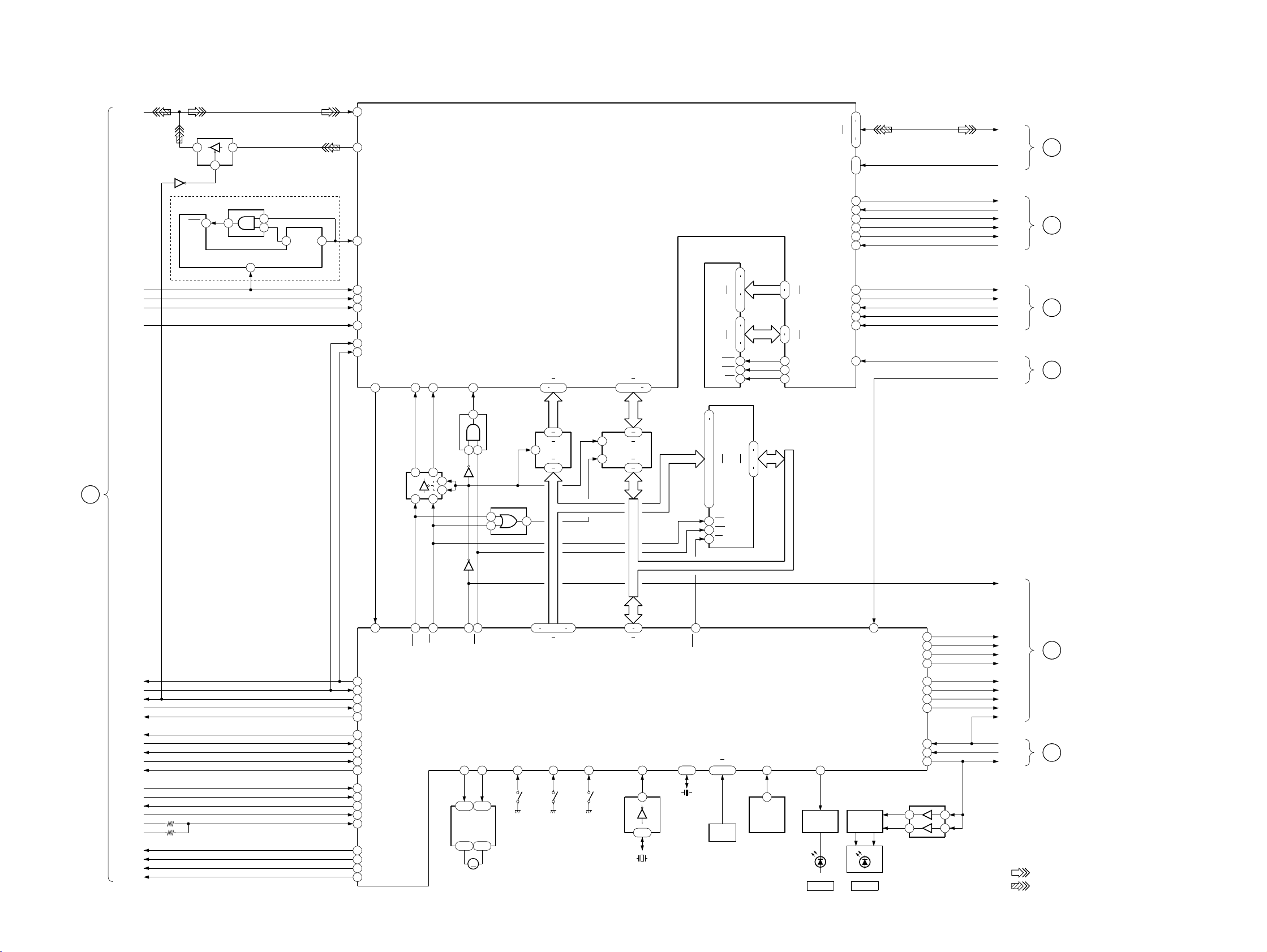
6-3. BLOCK DIAGRAM — MD CONTROL SECTION —
DPA-300
B
BD
SECTION
(Page 30)
DATA
LRCK
BCK
512FS
C2PO
IC2011
CLR
BUFFER
IC2003
1
1
26
DIVIDE-BY-6
CIRCUIT
IC2002
4
IC2001
CLK
2
5
DATA IN
6
DATA OUT
MD DATA
ENCODER/DECODER
IC2007
2
1
14
12QC
QA
10
WFCK
DRAM
IC2008
10
A0
13
9
LRCK
8
BCK
49
XTLI
7
C2PO
3
SQSY
98
XRST
93
XINT
BUFFER
IC2012
XCS96XRD
6
2
95
BUFFER
IC2010
3
5
1
7
IC2015
2 1
BUS
A0 A6
.
78 83
74
18 12
B1 B7
19
G
A1 A7
28
4
XWR
94
4
ADDRESS
BUFFER
IC2004
4
2
DIRECTION
OR
IC2006
2
1
DATA-BUS
BUFFER
IC2005
19
G
1
DIR
DB0 DB7
.
84 87.89
18 11
B1 B8
A1 A8
29
92
A9
I/O0
I/O7
RAS
CAS
WE
1M EEP ROM
IC2202
12
5
.
27
.
26
.
A0
23
.
25
.
A16
4
.
28
.
29
.
3
.
2
24
OE
31
WE
22
CE
.
16
20
.
9
2
5
.
24
27
8
23
7
13
D0
15
.
17
D7
21
MA0
37
38
21
14
22
23
24
MA9
MDB0
MDB7
XRAS
XCAS
XMWR
HDRQ/HSAC
XHAC/SDRQ
HDB0
HDB7
HA0
HA1
ADTO
ADTI
ACLK
XABS
AC2
XARQ
HINT
XHRD
XHWE
XHCS
66
64
.
62
58
53
.
.
54
43
42
41
44
45
46
56
69
70
67
68
55
D0-D7
HA0,1
ADTO
ADTI
ACLK
XALT
AC2
XARQ
HINT
DREQ1
DACK1
IORD
IOWR
MDCS
X.H RST
C
VIDEO
CONTROL
SECTION
D
AUDIO
SECTION
E
VIDEO
CONTROL
SECTION
F
VIDEO
PROCESS
SECTION
(Page 33)
(Page 43)
(Page 33)
(Page 36)
16
XRST
SQSY
REC
DQSY
XLAT
SWDT
SRDT
SCLK
SENS
SCTX
FOK
SHCK
WRPWR
LIMIT
PROTECT
REFLECT
SCL
SDA
LDON
MOD
19
DINT
28
XDRST
18
ATSY
34
RECPB
25
DQSY
30
XLAT
31
SWDT
32
SRDT
33
SCLK
78
SENS
24
SCTX
21
FOK
77
SHCK
22
WRPWR
92
LIMIT IN
93
PROTECT REFLECT
79
SCL
80
SDA
89
LDON
23
MOD
Q2002
DIG RST
.
.
OUT-SW
5
S191
LOAD OUT
DET
72 65
63
A0 A16
100
S192
LOAD IN
DET
61 54
PLAY-SW
SYSTEM CONTROL
REC-SW
7
S193
CHUCKING
DET
47
44
CS3
RD
26
11 10
LOADING MOTOR
29
46
XRST36
LD IN
1
.
17
LOADING
MOTOR
DRIVE
IC2301
.
913
M
M191
WR
LD OUT
2
.
.
A0 A6
IC2201
INVERTER
IC2203
88 81
10
3
.
17
X2202
32.768kHz
XCIN
XOUT
.
13 15
X2201
10MHz
50
CSO
XIN
KEY0
.
97 95
KEY
MATRIX
KEY2
.
94
RMC
6
2
REMOTE
CONTROL
RECEIVER
IC8101
BUSY
91
LED
DRIVER
Q8101
BUSY POWER
75
LED
DRIVER
Q8121,8122
D8121D8102
DA RST
DF LATCH
VOL DATA
X.H.RST
VOL CLK
HP VOL CE
LINE VOL CE
MIC MUTE
XAMUTE
POWER DOWN
5
7
RST
STB
27
26
35
37
73
3
4
76
20
12
38
LED
DRIVER
IC8121
DA RST
DF LAT
VOL DT
VOL CK
HP CE
LIN CE
M MUTE
AMUTE
P DWN
P DWN
S RST
STB
6
8
• Signal Path
G
AUDIO
SECTION
H
POWER
SECTION
: VIDEO (PB)
: VIDEO (REC)
(Page 43)
(Page 45)
— 31 — — 32 —
DPA-300
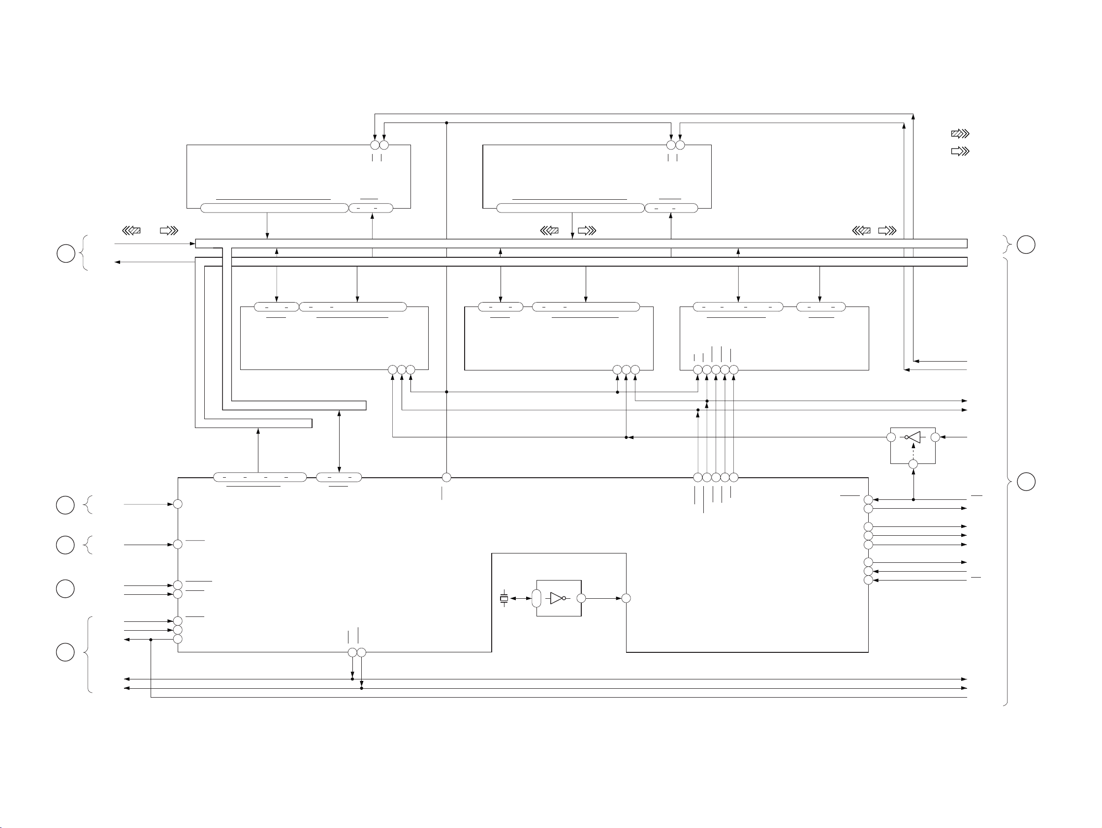
6-4. BLOCK DIAGRAM — VIDEO CONTROL SECTION —
CHINESE CHARACTER ROM
IC4015
• Signal Path
: VIDEO (REC)
12
10
CE
OE
PROGRAM ROM
IC4016
OE
1214
CE
: VIDEO (PB)
(Page 42)
(Page 40)
(Page 37)
(Page 32)
C
MD
CONTROL
SECTION
(Page 32)
I
VIDEO IN
SECTION
J
VIDEO OUT
SECTION
K
IR
SECTION
E
MD
CONTROL
SECTION
16
D0-7
HA0-1
IRQUART
DACK1
IORD
IOWR
D0-7
A1-2
22
23
24
27
28
13
12
D0
.17.19.22.24.26.28.14.16.18.20.23.25.27.29.
13
15
D0-15
D0-7
.
13 15 17 21
I/O1 I/O8 A0 A15
DATA-BUS D0-15
ADDRESS-BUS A1-23
A1-21,23
....
53 57 60 65 86 90 93 97 99
A1
INTP01VSYNC
INTP00M2FDO
INTP13/T1IRQSCC+
INTP12
INTP11HINT
DREQ/P03DREQ1
DACK/P04
12 5 27 26.2523
SRAM
IC4021
39 32 42 49
.
D0 D15A21 A23
D15
D0-15
.
A0
9 2 40 32 1
A1-16
..
IORD
2 3
A17
..
A1-18
DATA-BUS D0-15
ADDRESS-BUS A1-23
.31.
4
28..3
CE
NE
22 29 24
IOWR
OE
80
O0 O15
15
17.19.21.24.26.28.30.16.18.20.22.25.27.29.31
D8-15
.
13 15 17 21
I/O1 I/O8 A0 A15
MRD
X4002
4MHz
.
12 5 27 26
SRAM
IC4020
SYSTEM MICOM CPU
IC4003
1
.
7
INVERTER
IC4001
D0-15
A1-16
..4.28.
2523
2 71
.31.
3
OECENE
24 22 29
A0 A18
.
11 4 42 34 3 2
X1
...
A1-19
25710
D1 D15
CEUMWR
29 13 30
78 79 73 74 77
.
WE
UCAS
LCAS31RAS
LCAS
UCAS
LMWR/WE
DATA-BUS D0-15
ADDREDD-BUS A1-23
D0-15
3633.38.41
14
RAS
DRAM
IC4013
A1-10
17 20.23 28
A0 A9
DACK0/P02
DREQ0/P01
RESET
LCKOUT
CS1
CS2
CS3
INTP10
D0-15
A1-23
L
VIDEO
PROCESS
SECTION
(Page 35)
CS FONT1
CE
LMWR
SRAM DRIVE
IC4019
18
2
1G
1
UMWR
CS SRAM
M
30
68
83
84
85
14
15
29
RST
CLKIN
CS1
CS2
CS3
XDACK0
DRQ0
INT
IORD
IOWR
DACK1
VIDEO
PROCESS
SECTION
(Page 36)
— 33 — — 34 —
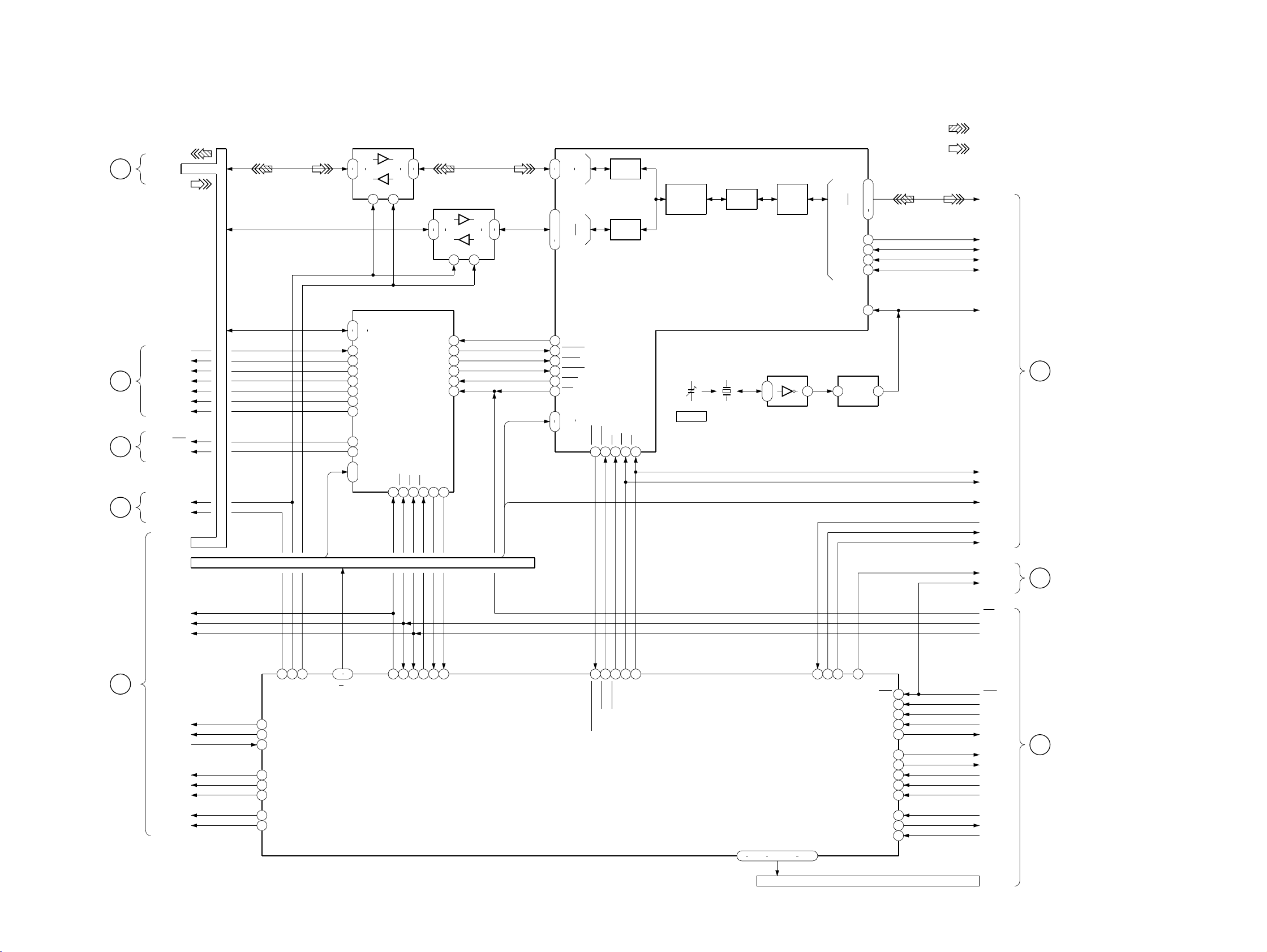
6-5. BLOCK DIAGRAM — VIDEO PROCESS SECTION —
DATA-BUS BUFFER
IC4010
HA1,2
2
A1
9
A8
DIR G
1
I/O DEMODULATOR
D0
31
D7
24
XMCWED12
VCOMUTE
16
PAL
18
NTSC
19
20
MUTE
43
OUT RESET
36
MI RESET
21
RST
BUZZER
38
5
A1
.
.
4
A2
(Page 34)
(Page 39)
(Page 42)
(Page 38)
L
VIDEO
CONTROL
SECTION
N
VIDEO
OUT
SECTION
O
VIDEO
IN
SECTION
P
IR
SECTION
D0-D15
XMCWED
VCO MUTE
NTSC
MUTE
IC3002 SEL
MI RST
RST
BEEP
BUF DIR
XBE MI
D0-15
D0-7
D8-15
DATA BUS D0-D15
D0-7
PAL
18
B1
11
B8
19
IC5004
50X RESET
RESET32WR35RD44CS
DATA-BUS BUFFER
IC4011
2
A1
9
A8
DIR G
1
END
10
37
STDBY
9
CLKEN
8
DINT
11
50X INT
13
DMA SEL0VDD
DMA SEL1
2
6
7
DPA-300
• Signal Path
: VIDEO (REC)
: VIDEO (PB)
91
DATA0
84
DATA7
82
.
18
B1
11
B8
19
HA1-10
HA1,2
81
79
74
58
59
64
92
100
12
.
3
CODE0
CODE7
END14
RESET
STBY
CLKEN
DINT
INT
ADDR0
ADDR9
DREQ
93
HOST
I/O
CODE
I/F
DACK95CS96WR97RD
98
ENCODE/
DECODE
UNIT
JPEG IMAGE
COMPRESSION/
DECOMPRESSION
PROCESSOR
CT4001
CLOCK
DCT
UNIT
IC4007
X4003
24.54545MHz
PIXEL
DATA
INVERTER
IC4008
1
.
3
PIXEL4
I/F
PIXEL11
CLOCK DIVIDER
5 1 5
COMP
STOP
EOS
DSYNC
DCLK
IC4009
48
.
47
.
45
40
33
36
37
39
63
QCK
PIX0-7
COMP
STOP
EOS
DSYNC
CLK
XRD
XWR
HA1,2
XDREQ
XDACK
XCS
R
VIDEO
OUT
SECTION
(Page 39)
(Page 37)
Q
IR
SECTION
HA1-6
RST OUT
IOWR
IORD
DACKIR
IRAEN
IRDRQX
CS 102
XH CS IR
H CS IRS
XIRD3
XIWR3
16
DACKIR6
IRAEN
5
IRDROX
4
84
CS 102
7
XH CS IR
8
XH CS IRS
XIRD3
2
XIWR3
3
44
XBE M1
37
45
BUF DIR
BE 50
ADDRESS BUS HA1-6
HA1-10
34 25
HA1 HA10
95
10
RST OUT
94
IOWR
83
IORD
17
CS IO1
DMA SEL0
18
DMA SEL1
GATE ARRAY
IC4004
36
43
40
DACK 5041XHCS 50
MD3605X DREQ
39
XWR2
XRD2
A1 - 10,16,19,21,23
52 58
69
67 70
.
.
72
79
19
47
93
MD CS
DACK M149XHCS M1
DREQ M1
CE ROM8M0
CS FONT1
..
74
ADDRESS BUS A1-23
RST
CLK IN
LMWR
UMWR
CS SRAM
CS1
CS2
CS3
DACK1
DRQ0
XDACK0
100
MD CS
X.H.RST
INT
IOWR
IORD
12
62
80
81
22
82
89
90
91
77
78
96
RST
CLK IN
LMWR
UMWR
CE
CS SRAM
CS FONT1
CS1
CS2
CS3
DACK1
DRQ0
XDACK0
A1-23
F
MD
CONTROL
SECTION
M
VIDEO
CONTROL
SECTION
(Page 32)
(Page 34)
— 35 — — 36 —
DPA-300
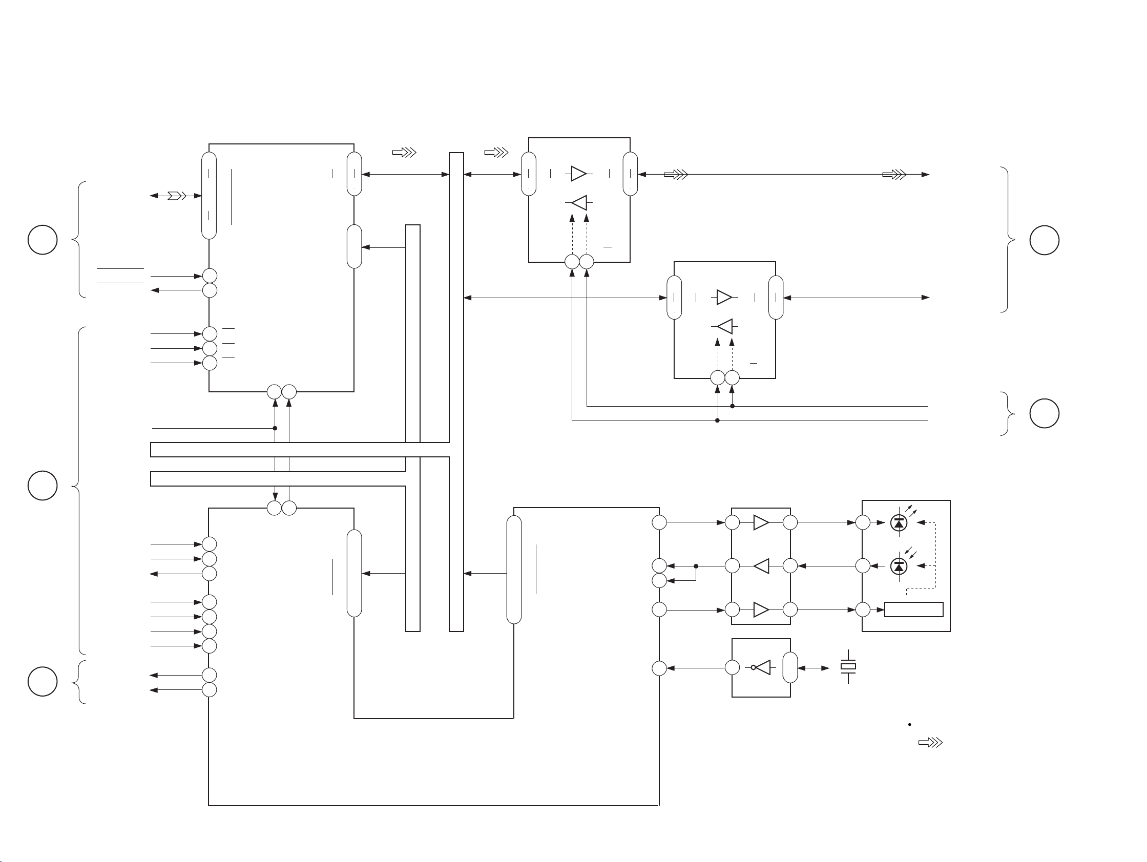
6-6. BLOCK DIAGRAM — IR SECTION —
S
VIDEO
IN
SECTION
(Page 42)
Q
VIDEO
PROCESS
SECTION
(Page 35)
K
VIDEO
CONTROL
SECTION
(Page 33)
14
P10
16
D0-7
HOST STB
VIN BUSY
CS-102
IOWR
IORD
RST-OUT
D0-15
HA1-6
DACKIR DACKX
XH CS IR
IRDRQX
H CS IRS
IRAEN
XIRD3
XIWR3
IRQUART
IRQSCC+
.
18
22
11
12
2
35
44
48
79
86
92
93
94
82
83
P17
P11
P22
CS
WR
RD
SA15
DRQX
SETUP
AEN
IOR
IOW
IRQUART
IRQSCC+
I/O DEMODULATOR
IC5003
RESET
P00
32 43
DATA-BUS D0-15
ADDRESS-BUS HA1-6
181654
IRBUSY
REGISTORV
31
D0
24
D7
5
A1
..
A2
4
20
.
SA0
21
.
23
.
28
.
30
.
SA5
32
D0-7
HA1-2
HA1-6
IR CONTROLLER
IC5002
D0-7
D8-15
HA1-6
60
61
64
65
68
69
71
72
DATA-BUS BUFFER
2
A1
A8
9
DIG
.
SO0
.
.
.
.
.
SO7
.
IC4006
1
19
B8
B1
ENABLE
G
RXDIR
RXDSH
GAINCTRL
11
18
TXO
CLK
DATA-BUS BUFFER
2
A1
A8
9
DIG
7
96
97
6
90
IC4005
1
19
11
B8
B1
ENABLE
G
BUFFER
IC112
2
9
5
INVERTER
IC5001
11
18
12
8
1
3
D0-7 MAR
T
VIDEO
OUT
SECTION
D8-15 MAR
BUFDIR
XBE MI
IRDA
RECEIVER/TRANSMITER
IC8001
3
.
7
2
6
36.864MHz
CONTROL
X4001
Signal Path
:VIDEO(PB)
(Page 39)
P
VIDEO
PROCESS
SECTION
(Page 35)
16
— 37 — — 38 —
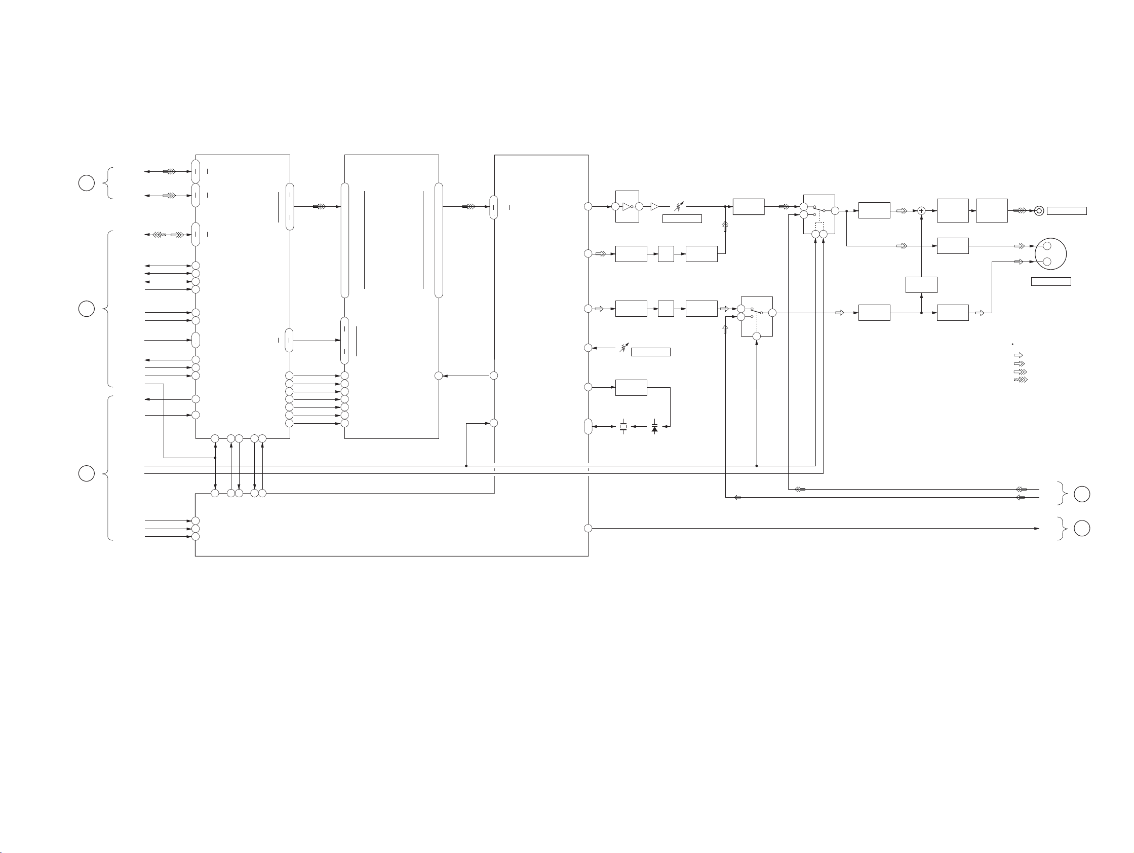
6-7. BLOCK DIAGRAM — VIDEO OUT SECTION —
DPA-300
T
IR
SECTION
(Page 38)
R
VIDEO
PROCESS
SECTION
(Page 36)
D0-7 MAR
D8-15 MAR
PIX0-7
DSYNC
EOS
STOP
COMP
XRD
XWR
HA1-2
XDREQ
XDACK
XCS
CLK
XMCWED
MI RST
PICTURE MEMORY CONTROLLER
25
18
1710D8
D15
81
PIX0
88
PIX7
DSYNC
91
92
EOS
STOP
93
94
COMP
128
XRD
1
XWR
8
.
7
XDRQ
2
3
XDACK
XCS
127
WEND
5
XRST
125
D0
D7
A1
.
A2
CLK
98 78
IC1005
ADRQ
77
ADAKADRAQN
75
SCLKSIOCLK
SDATSIODAT
73
VD0
VD15
VA0
VA8
OW1
WEL
WEH
RAS1
CAS
DSF
SE1
RAM
IC1003
5
63
56
.
54
47
29
37
.
7
.
10
.
12
.
15
.
17
.
20
.
22
.
43
.
45
.
48
.
50
.
53
.
55
.
58
.
60
37
34
.
31
27
271
2445
2544
2643
3940
4138
6369
W0/IO0
W15/IO15
A0
A8
DTX/OEX
LWEX
UWEX
RAS
CAS
DSF
SEX
SIO0
SIO15
4
.
6
.
9
.
11
.
14
.
16
.
19
.
21
.
44
.
46
.
49
.
51
.
54
.
56
.
59
.
61
SC
64
DIGITAL NTSC ENCODER
7691DIN0
DIN15
RAMSCK
74
YCON
57
IC2003
YDAO
CDAO
YVREF
NCPO
VXONI
.
VXONO
VDO
INVERTER
IC3004
62 6 7
46
33
43
27
8
.
7
Y BUFFER
Q3001
C BUFFER
Q3002
IC2002
LPF
X2001
14.31818MHz
Q3020 RV3003
RV3001
WHITE LEVEL
D2001,2002
SYNC LEVEL
LPF
LPF
Y BUFFER
Q3003
C BUFFER
Q3002
Y AMP
Q3016,3019
VIDEO SWITCH
IC3001
1
3
SW1
2
VIDEO SWITCH
IC3002
3
5
SW2
SW1
2
4
7
Y BUFFER
7
Q3010,3011
C BUFFER
Q3014
C BUFFER
Q3005-3007
VIDEO
AMP
Q3012,3013
Y BUFFER
Q3101,3102
C BUFFER
Q3013,3104
VIDEO
BUFFER
Q3017,3018
J106
VIDEO OUT
J104
3
4
YC(S) OUT
Signal Path
: CHROMA
: Y
: VIDEO (PB)
: VIDEO (REC)
N
VIDEO
PROCESS
SECTION
(Page 35)
16
MUTE
IC3002SEL
VCOMUTE
NTSC
PAL
58
59
60
65 72
MKTGI
VCOMUTE
NTSC
PAL
73
ADRREQ
70
71
FDO
64
VIN Y
VIN C
M2FD0
U
VIDEO IN
SECTION
J
VIDEO
CONTROL
SECTION
(Page 42)
(Page 33)
— 39 — — 40 —
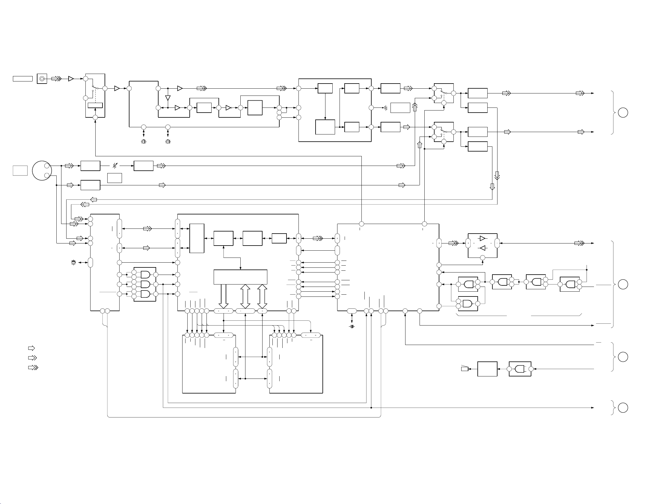
DPA-300
6-8. BLOCK DIAGRAM — VIDEO IN SECTION —
VIDEO IN
SWITCH
IC201
1
3
LOGIC
2
CTLA
Q403
7
4FSC CLOCK
GENERATOR
IC402
V2 IN26
32FH
X401
500kHz
VIDEO IN
J102
Q401
DIGITAL COMB FILTER,
Y/C SEP
IC401
30
8
14.3M
11
X402
14.3MHz
Q404,421
Q406
Q405
Y
H SYNC
2
SEP.
Q408
22
BURST
BGP O
GATE
23 20
PULSE
BGP I
4FSC OUT
19
17
VO1
C IN
5
AD IN
25
CLPI
17
11
OCLK
A/D
CONV.
ADAPTIV
FILTER
OPRATION
D/A
CONV.
D/A
CONV.
AY0
VCC
CY0
Y BUFFER
31
Q408.411
RV402
33
39
Y OUT PUT
C BUFFER
Q409,412
LEVEL
Y INPUT
SELECTOR
IC203
1
3
2
C INPUT
SELECTOR
IC202
1
3
2
Y BUFFER
7
7
Q416
Y BUFFER
Q414
C BUFFER
Q415
C BUFFER
Q413
VIN Y
VIN C
U
VIDEO
OUT
SECTION
(Page 40)
J101
S VIDEO
IN
3
4
• Signal Path
: CHROMA
: Y
: VIDEO
X101
26.798MHz
Y BUFFER
Q407
Q407
C BUFFER
Q410
17
13
19
15
65
.
66
FRONT-END
IC104
AI31
AI41
AI22
AI32
XTALI
XTAL
HSYNC
VSYNC
ODD/EVEN
SCL
6
SCL
RV403
S INPUT
Y LEVEL
DY0
DY7
DUV0
DUV7
LLC2
SDA
5
SDA
Y BUFFER
Q419,420
JPEG
CASY
73
29
URAS
CASC
L CAS
ENCODER/DECODER
IC105
DCT/IDCT
AND
Q/Q-1
DRAM I/F
CONTROL
A0-8
.
.
A0 A8
DQ1
DQ8
DQ9
DQ16
93
26
64 59 56
2
5
.
7
10
31
34
.
37
39
83 87 90
16 19 22
AND
ENCODER
AND
DECODE
AD0-7
.
.
55
74 81
BD0-7
36
61
SEL S/O
I/O SEL
HSTBI
HHDET
HSTBO
HD0
HD7
HCLR
DATA-BUS BUFFER
IC110
DIR
1
BUZZER
SWITCH
Q103
18
B1
11
B8
IC111
IC109
3
1
2
16
IC109
11
12
13
69
IC109
4
5
NAND GATE
INVERTER
IC106,109
BUZZER CONT.
D0-7
B+
VIN BUSY
HOST STB
RST
S
IR
SECTION
(Page 37)
O
VIDEO
BEEP
PROCESS
SECTION
(Page 35)
22
15
37
41
39
38
BZ101
BUZZER
2
A1
9
A8
IC106
8
12
13
10
IC106
11
62
I/F
14
28
RAS
2
DQ1
5
.
7
DQ8
10
31
DQ9
34
.
37
DQ16
39
29
URAS
HA0
HA1
RSTI
DACK
DREQ
50
27OE13
L CAS
.
WR
RD
CS
INT
OE2
20
6
.
7
3
4
5
1
8
10
11
WE2
51
.
16 19 22
26
A0 A8
W
DRAM
IC102
13
D0-7
HOST
D0
14
7
D7
2
HA0
.
.
1
HA1
5
WR
4
RD
3
CS
6
RSTO
64
DACK
46
DREQ
45
INT
XTALO
13 15
X102
16MHz
SEL R/F
VIDEO INPUT
CONTROL MICOM
IC108
.
XTAL
ODD/EVEN
.
VSYNC31IICLK50IICDATA49RSTI
29
SDA
SCL
27
54
.
53
.
50
45
62
55
30
1
38
2
4
41
5
12
40
13
V/H SYNC
NAND GATE
3
6
11
IC103
30
27
Y0-7
.
24
21
39
35
C0-7
.
33
31
MCLK98
HBLK
42
VBLK
43
ODV/EVEN
44
PIXEL
OE1
WE1
52
53
27OE13W14
I/F
54
RAS
65
28
RAS
DRAM
IC101
V SYNC
16
I
VIDEO
CONTROL
SECTION
(Page 33)
— 41 — — 42 —
 Loading...