

Sony DNF-610 Service manual
D-NF610/NF611
SERVICE MANUAL
Ver 1.4 2005.06
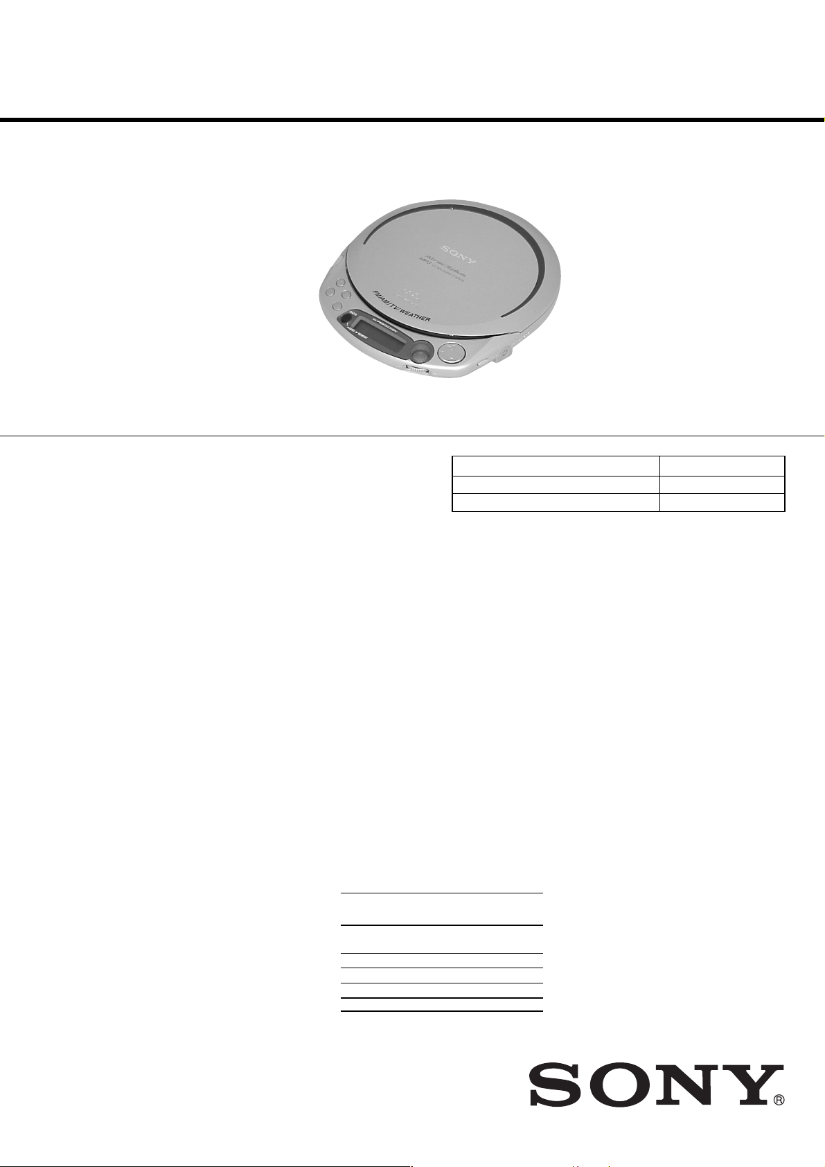
Photo : D-NF610
SPECIFICATIONS
CD player
System
Compact disc digital audio system
Laser diode properties
Material: GaAlAs
Wavelength: λ = 780 nm
Emission duration: Continuous
Laser output: Less than 44.6 µW
(This output is the value measured at a distance
of 200 mm from the objective lens surface on
the optical pick-up block with 7 mm aperture.)
D-A conversion
1-bit quartz time-axis control
Frequency response
20 - 20 000 Hz
307)
Output (at 4.5 V input level)
Headphones (stereo minijack)
Approx.5 mW + Approx. 5 mW at 16 Ω
Radio
Frequency range (9k/10k switch)
•9 kHz step:
TV: 2 - 13 ch
WB (weather band): 1 - 7 ch
FM: 87.5 - 108.0 MHz
AM: 531 - 1 710 kHz
•10 kHz step:
TV: 2 - 13 ch
WB (weather band): 1 - 7 ch
FM: 87.5 - 108.0 MHz
AM: 530 - 1 710 kHz
+1
dB (measured by JEITA CP-
–2
Antenna
FM: Headphones/earphones cord antenna
AM: Built-in ferrite bar antenna
General
Power requirements
For the area code of the model you
purchased, check the upper left side of the
bar code on the package.
•Two LR6 (size AA) batteries: 1.5 V DC × 2
•AC power adaptor (DC IN 4.5 V jack):
U, U2, CND, E92, MX and TW models:
120 V, 60 Hz
AEP, EE, EE1, E, E13
and E13/2 models: 220 - 230 V, 50/60 Hz
CEK model: 230 V, 50 Hz
AUS model: 240 V, 50 Hz
EU8, EU8/C, JE.W, E18, KR and EE8
models: 100 - 240 V, 50/60 Hz
HK model: 230 V, 50 Hz
Battery life*1 (approx. hours)
(When you use the CD player on a flat and stable
surface.)
Playing time varies depending on how the CD
player is used.
When using two Sony alkaline batteries
LR6 (SG) (produced in Japan)
G-PROTECTION
Audio CD 48 43
ATRAC3plus files*
MP3 files*
RADIO ON 62
2
3
US Model
Canadian Model
AEP Model
UK Model
E Model
Model Name Using Similar Mechanism NEW
CD Mechanism Type CDM-3325ER2
Optical Pick-up Name DAX-25E
*1 Measured value by the standard of JEITA
(Japan Electronics and Information Technology
Industries Association)
*2 When recorded at 48 kbps or 64 kbps
*3 When recorded at 128 kbps
Operating temperature
5°C - 35°C (41°F - 95°F)
Dimensions (w/h/d) (excluding
projecting parts and controls)
Approx. 136.0 × 25.4 × 156.3 mm
3
⁄8× 1 × 6 1⁄4 in.)
(5
Mass (excluding accessories)
Approx. 215 g (7.6 oz.)
Design and specifications are subject to change
without notice.
•Abbreviation
AUS: Australian model
CND : Canadian model
E13 : 220-230 V AC area in E model
E92 : 120 V AC area in E model
EE : East European model
HK : Hong Kong model
KR : Korean model
MX : Mexican model
“1” “2”
75 75
70 70
TW : Taiwan model
PORTABLE CD PLAYER
D-NF610
D-NF611
9-877-312-05
2005F16-1
© 2005.06
Sony Corporation
Personal Audio Group
Published by Sony Engineering Corporation

D-NF610/NF611
TABLE OF CONTENTS
1. SERVICING NOTE ·························································· 3
2. GENERAL ·········································································· 4
3. DISASSEMBLY ································································ 5
4. ELECTRICAL ADJUSTMENT ···································· 8
5. DIAGRAMS······································································ 10
5-1. Block Diagram
– MAIN Section – ······················································· 11
– TUNER Section – ····················································· 12
5-2. Printed Wiring Board
– MAIN Board (Side A)(1/2) – ··································· 13
5-3. Printed Wiring Board
– MAIN Board (Side A)(2/2) – ··································· 14
5-4. Printed Wiring Board – MAIN Board (Side B)(1/2) – 15
5-5. Printed Wiring Board – MAIN Board (Side B)(2/2) – 16
5-6. Schematic Diagram – MAIN Board (1/5) – ··············· 17
5-7. Schematic Diagram – MAIN Board (2/5) – ··············· 18
5-8. Schematic Diagram – MAIN Board (3/5) – ··············· 19
5-9. Schematic Diagram – MAIN Board (4/5) – ··············· 20
5-10.Schematic Diagram – MAIN Board (5/5) – ··············· 21
5-11.IC Block Diagram ······················································· 22
5-12.IC Pin Function Descriptions ······································ 27
6. EXPLODED VIEWS ······················································ 32
7. ELECTRICAL PARTS LIST ······································· 35
This appliance is classified as a CLASS 1 LASER product.
The CLASS 1 LASER PRODUCT MARKING is located on
the rear exterior.
CAUTION
Use of controls or adjustments or performance of procedures
other than those specified herein may result in hazardous
radiation exposure.
Flexible Circuit Board Repairing
•Keep the temperature of the soldering iron around 270 ˚C during repairing.
• Do not touch the soldering iron on the same conductor of the
circuit board (within 3 times).
• Be careful not to apply force on the conductor when soldering
or unsoldering.
Notes on chip component replacement
•Never reuse a disconnected chip component.
• Notice that the minus side of a tantalum capacitor may be damaged by heat.
Notes on the power source
Disconnect all power sources when the CD player is not used for a long time.
Unleaded solder
Boards requiring use of unleaded solder are printed with the leadfree mark (LF) indicating the solder contains no lead.
(Caution: Some printed circuit boards may not come printed with
the lead free mark due to their particular size.)
: LEAD FREE MARK
Unleaded solder has the following characteristics.
• Unleaded solder melts at a temperature about 40°C higher than
ordinary solder.
Ordinary soldering irons can be used but the iron tip has to be
applied to the solder joint for a slightly longer time.
Soldering irons using a temperature regulator should be set to
about 350°C.
Caution: The printed pattern (copper foil) may peel away if the
heated tip is applied for too long, so be careful!
• Strong viscosity
Unleaded solder is more viscous (sticky, less prone to flow) than
ordinary solder so use caution not to let solder bridges occur such
as on IC pins, etc.
• Usable with ordinary solder
It is best to use only unleaded solder but unleaded solder may
also be added to ordinary solder.
On AC power adaptor
• Use only the AC power adaptor supplied.
If your CD player is not supplied with the one, use the AC-E45HG AC
power adaptor. Do not use any other AC power adaptor. It may cause a
malfunction.
Polarity of the plug
• Do not touch the AC power adaptor with wet hands.
• Connect the AC power adaptor to an easily accessible AC outlet. Should
you notice an abnormality in the AC power adaptor, disconnect it from
the AC outlet immediately.
SAFETY-RELATED COMPONENT WARNING!!
COMPONENTS IDENTIFIED BY MARK 0 OR DOTTED LINE WITH
MARK 0 ON THE SCHEMATIC DIAGRAMS AND IN THE PARTS
LIST ARE CRITICAL TO SAFE OPERATION. REPLACE THESE
COMPONENTS WITH SONY PARTS WHOSE PART NUMBERS
APPEAR AS SHOWN IN THIS MANUAL OR IN SUPPLEMENTS
PUBLISHED BY SONY.
2
ATTENTION AU COMPOSANT AYANT RAPPORT
À LA SÉCURITÉ!
LES COMPOSANTS IDENTIFÉS PAR UNE MARQUE 0 SUR LES
DIAGRAMMES SCHÉMATIQUES ET LA LISTE DES PIÈCES SONT
CRITIQUES POUR LA SÉCURITÉ DE FONCTIONNEMENT. NE
REMPLACER CES COMPOSANTS QUE PAR DES PIÈSES SONY
DONT LES NUMÉROS SONT DONNÉS DANS CE MANUEL OU
DANS LES SUPPÉMENTS PUBLIÉS PAR SONY.
SECTION 1
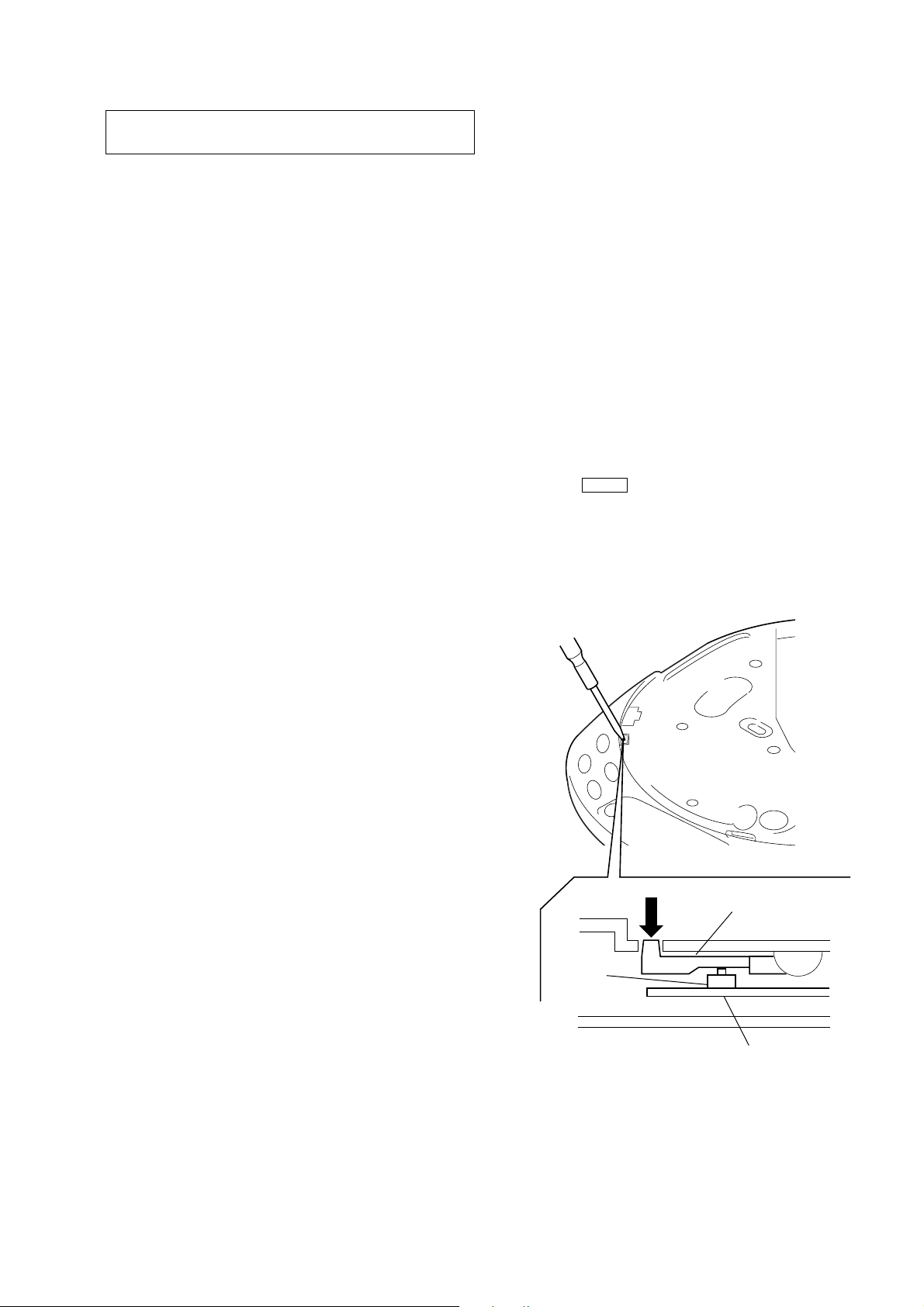
S820
detection lever
MAIN board
SERVICING NOTE
D-NF610/NF611
NOTES ON HANDLING THE OPTICAL PICK-UP
BLOCK OR BASE UNIT
The laser diode in the optical pick-up block may suffer electrostatic
breakdown because of the potential difference generated by the
charged electrostatic load, etc. on clothing and the human body.
During repair, pay attention to electrostatic breakdown and also use
the procedure in the printed matter which is included in the repair
parts.
The flexible board is easily damaged and should be handled with
care.
NOTES ON LASER DIODE EMISSION CHECK
The laser beam on this model is concentrated so as to be focused on
the disc reflective surface by the objective lens in the optical pickup block. Therefore, when checking the laser diode emission,
observe from more than 30 cm away from the objective lens.
BEFORE REPLACING THE OPTICAL PICK-UP BLOCK
Please be sure to check thoroughly the parameters as par the “Optical
Pick-Up Block Checking Procedures” (Part No.: 9-960-027-11)
issued separately before replacing the optical pick-up block.
Note and specifications required to check are given below.
• FOK output: IC601 yg pin
When checking FOK, remove the lead wire to disc motor.
• RF signal P-to-P value: 0.4 to 0.6 Vp-p
LASER DIODE AND FOCUS SEARCH OPERATION
CHECK
During normal operation of the equipment, emission of the laser
diode is prohibited unless the upper lid is closed while turning ON
the S801. (push switch type)
The following checking method for the laser diode is operable.
• Method:
Emission of the laser diode is visually checked.
1. Open the upper lid.
2. With a disc not set, turn on the S820 with a screwdriver having a
thin tip as shown in Fig.1.
3. Press the > B button.
4. Observing the objective lens, check that the laser diode emits
light.
When the laser diode does not emit light, automatic power control
circuit or optical pickup is faulty.
In this operation, the objective lens will move up and down 4
times along with inward motion for the focus search.
Fig. 1 Method to push the S820
3
D-NF610/NF611
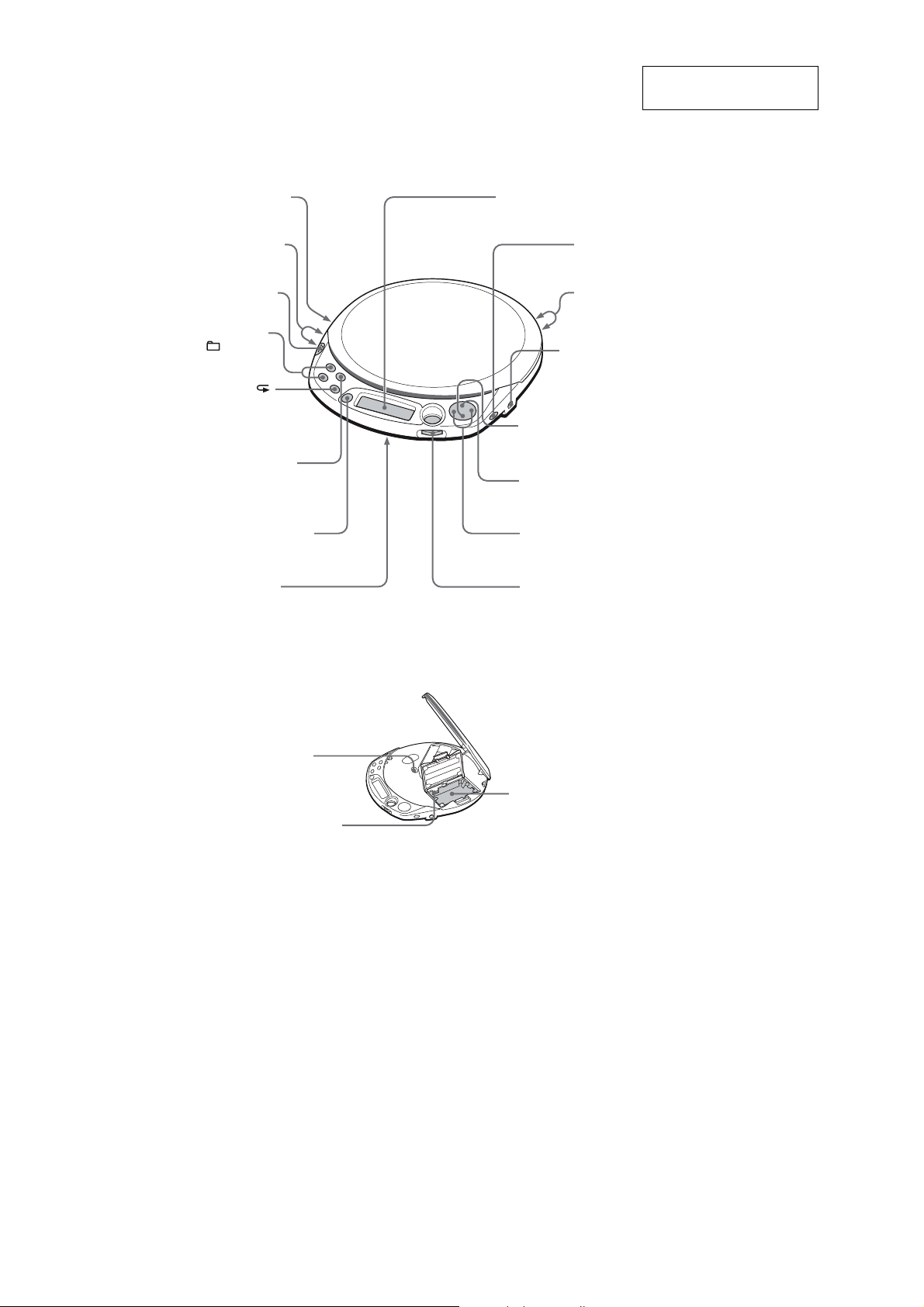
CD player (front)
SECTION 2
GENERAL
This section is extracted
from instruction manual.
1 i (headphones)
jack
(pages 11, 29)
2 VOL (volume)
+*/– buttons
(page 11)
3 OPEN button
(page 11)
4 TUNE +/–•
+/– buttons
(pages 12, 21)
5 P MODE/
(play mode/repeat)
button
(pages 16 - 19, 22)
6 DISPLAY button
(pages 23, 26, 27)
7 RADIO ON•BAND/
MEMORY button
(pages 21 - 25)
8 HOLD switch
(page 28)
*The button has a tactile dot.
9 Display
(pages 13, 16, 19 - 24, 26 - 28)
q; SOUND button
(pages 27, 28)
qa Strap holes
qs DC IN 4.5 V
(external power
input) jack
(page 30)
qd x (stop)•RADIO OFF
button
(pages 12, 21, 24, 28)
qf u* (play/pause) button
(pages 11, 12, 16, 18, 19)
qg ./> (AMS/search)•
PRESET –/+ buttons
(pages 12, 16, 19, 24, 25)
qh JOG DIAL/
ENTER (pages 16, 20)
CD player (inside)
qj G-PROTECTION
switch (page 26)
qk 9k/10k switch (page 25)
Exept European model .
ql Battery compartment
(page 30)
4
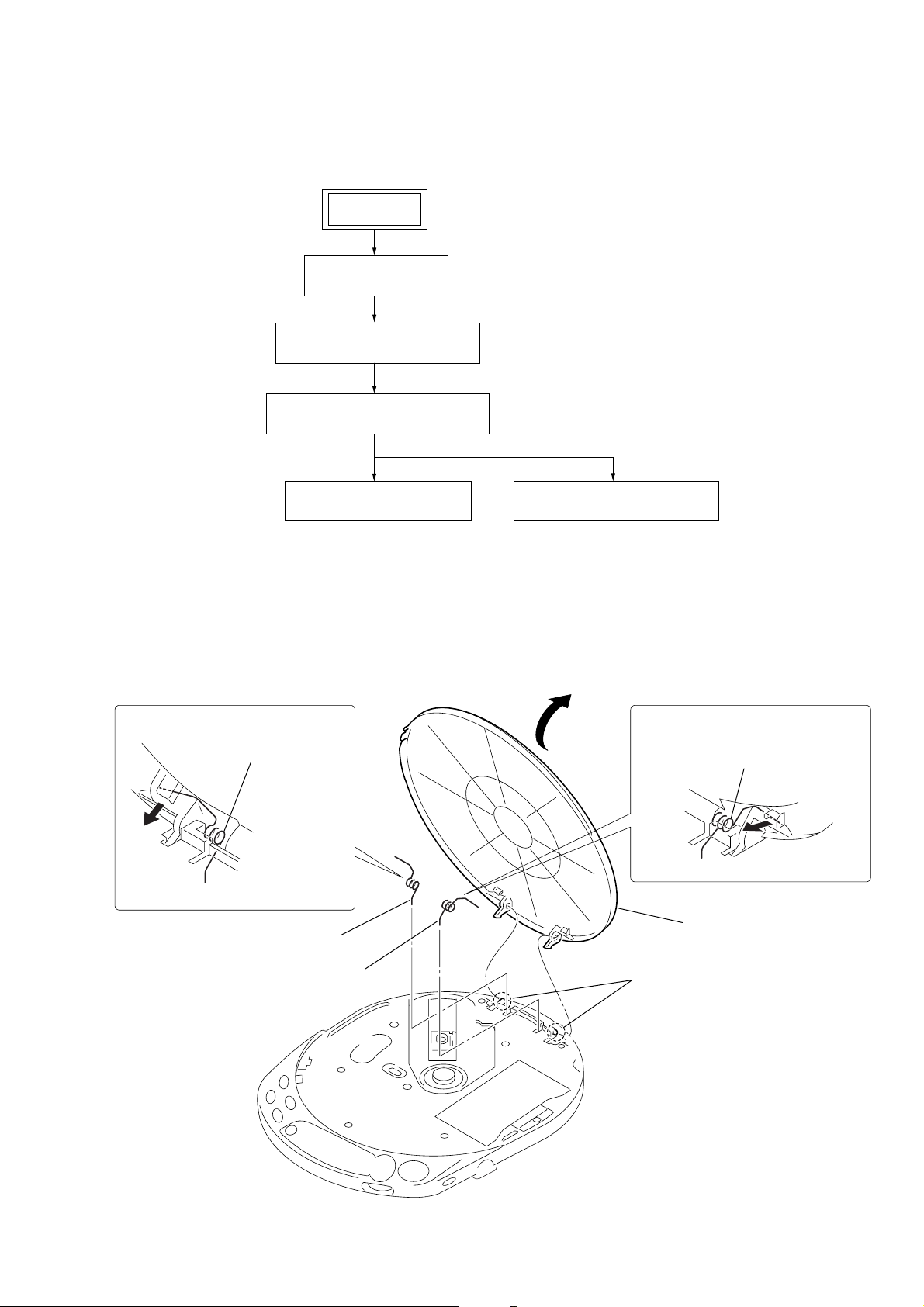
DISASSEMBLY
3
two claws
4
spring (L)
5
spring (R)
6
lid (upper) assy
1
Remove the open spring (L) in
the direction of the arrow.
2
Remove the open spring (R) in
the direction of the arrow.
Note : Disassemble the unit in the order as shown below.
SET
LID (UPPER) ASSY
CABINET (FRONT) ASSY
CD MECHANISM (CDM-3325ER2)
MAIN BOARD
D-NF610/NF611
SECTION 3
Note : Follow the disassembly procedure in the numerical order given.
3-1. Lid (Upper) Assy
TURN TABLE MOTOR ASSY
(SPINDLE) (M901)
MOTOR ASSY (SLED) (M902),
OPTICAL PICK-UP (DAX-25E)
5
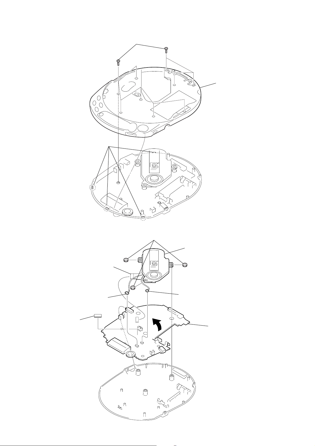
D-NF610/NF611
y
d
3-2. Cabinet (Front) Assy
2
four claws
1
nine screws (B2)
3
cabinet (front) ass
3-3. CD Mechanism (CDM-3325ER2), MAIN Board
4
flexible board
(15P) (CN601)
2
connector (CN402)(4P)
1
sheet
5
three insulators
6
CD mechanism
(CDM-3325ER2 )
3
connector (CN401)(2P)
7
MAIN boar
6
y
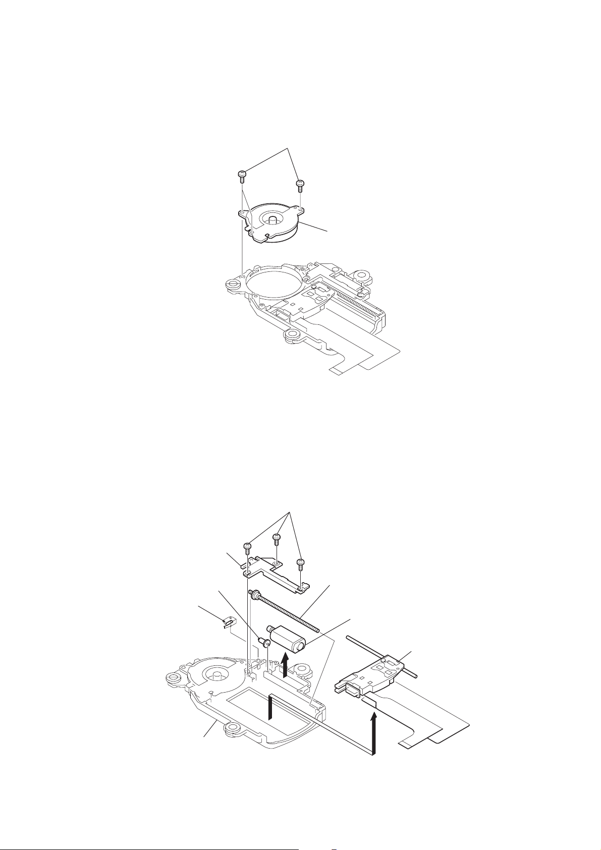
3-4. Turn Table Motor Assy (Spindle)(M901)
1
three screws
(B1.7
×
4)
2
turn table motor ass
(spindle) (M901)
D-NF610/NF611
3-5. Motor Assy (SLED)(M902), Optical Pick-Up (DAX-25E)
1
three screws
×
4)
5
2
gear cover
6
sled spring
4
gear B
(B1.7
feed screw assy
3
motor assy
(sled) (M902)
7
optical pick-up
(DAX-25E)
chassis
7
D-NF610/NF611
p
SECTION 4
ELECTRICAL ADJUSTMENT
The CD section adjustments are done automatically in this set.
Precautions for Check
1. Perform check in the order given.
2. Use YEDS-18 disc (Part No.: 3-702-101-01) unless otherwise
indicated.
3. Power supply voltage requirement : DC4.5 V in DC IN jack.
(J401)
VOLUME : Minimum
AVLS : OFF
HOLD switch : OFF
[MAIN board] (Side A)
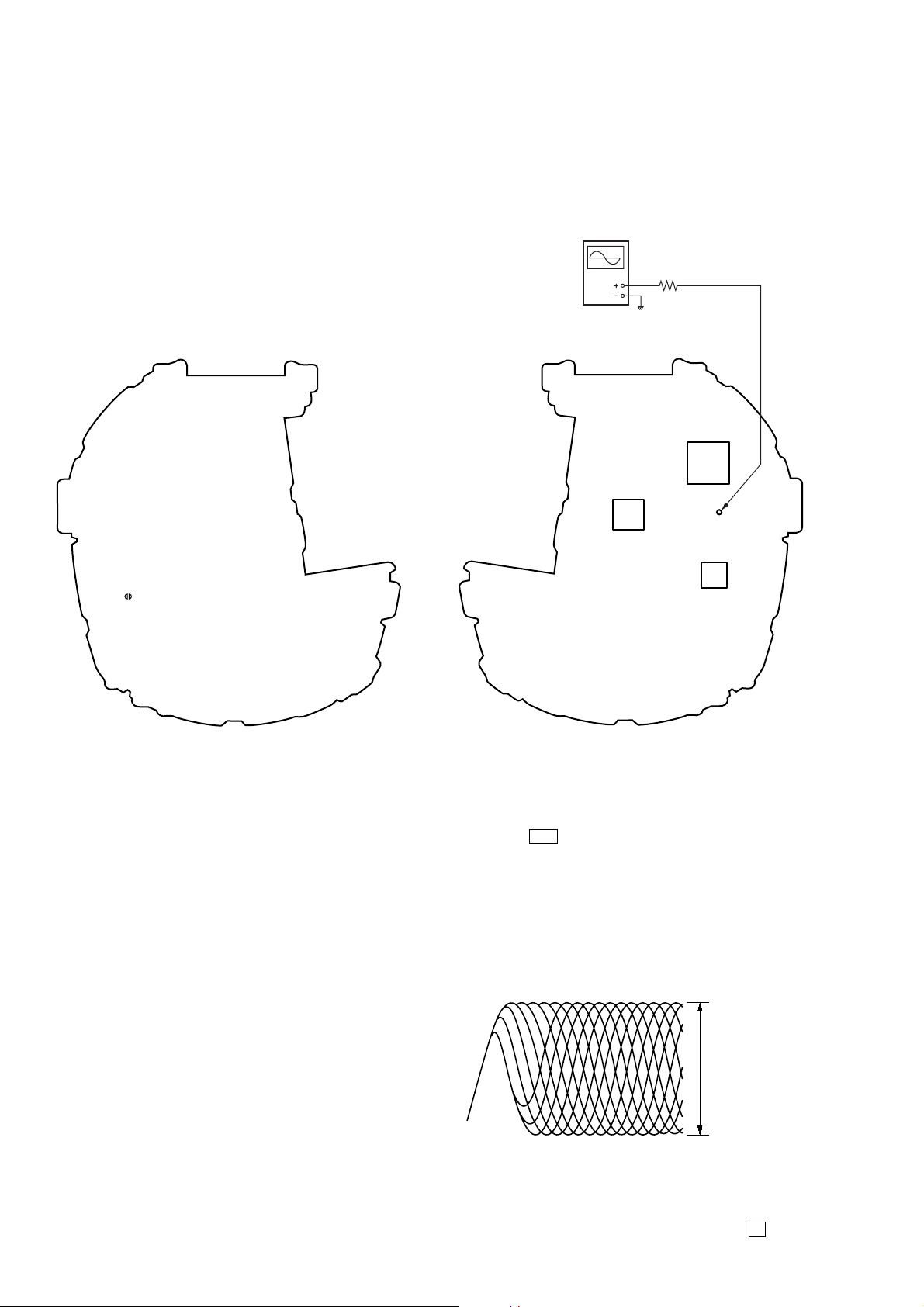
Focus bias Check
Condition:
• Hold the set in horizontal state.
• Terminate TAP805 (open) by solder.
Connection:
Oscilloscope
(AC range)
[MAIN board] (Side B)
IC3
IC601
TJ601
(RF)
TAP805
(OPEN)
IC301
Procedure:
1. Connect the oscilloscope to the test points TJ601 (RF) on the
MAIN board.
2. Set a disc. (YEDS-18)
3. Press the u button.
4. Check the oscilloscope waveform is as shown below.
A good eye pattern means that the diamond shape (◊) in the
center of the waveform can be clearly distinguished.
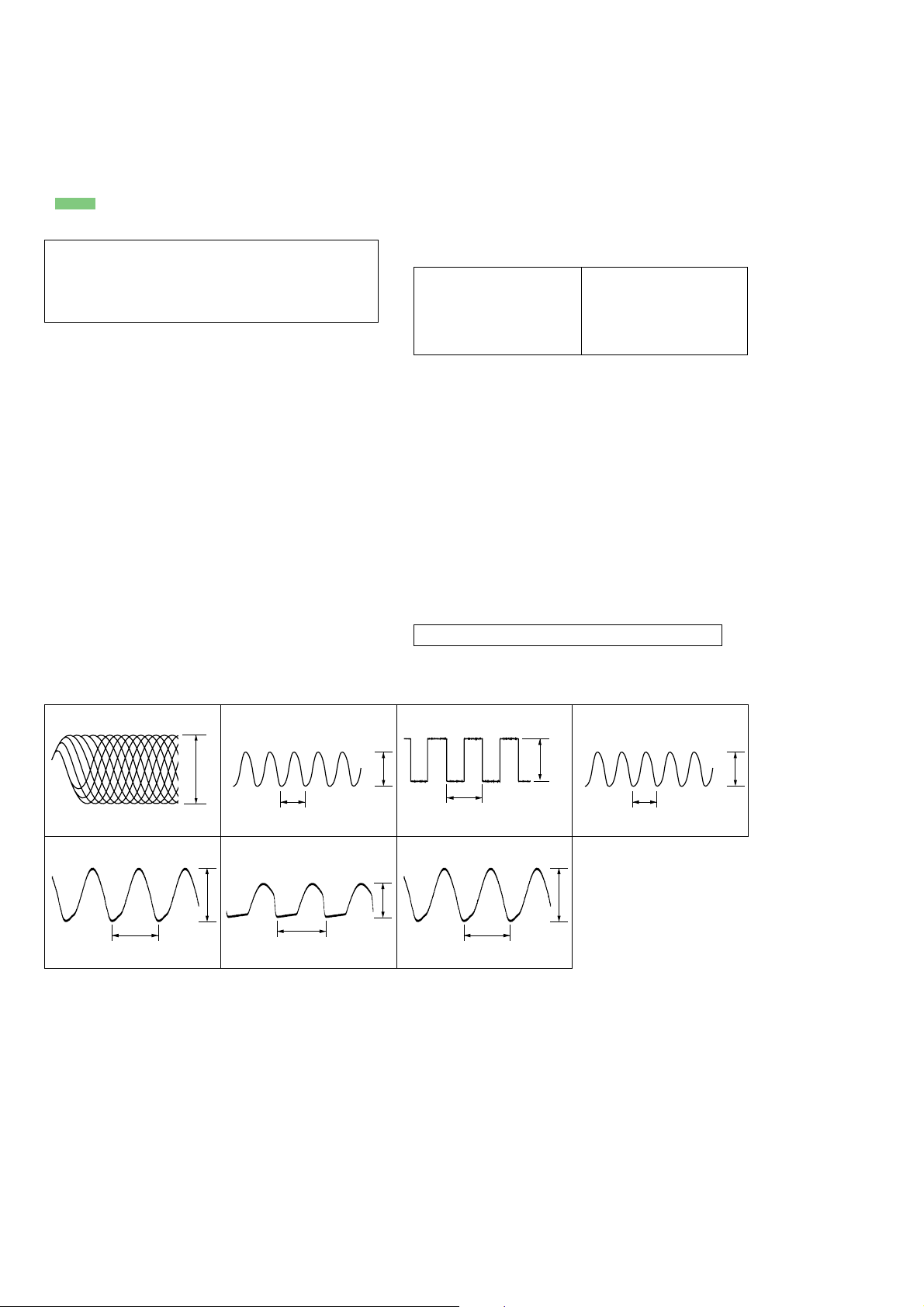
RF Signal reference Waveform (Eye Pattern)
VOLT/DIV : 20 mV (With the 10:1 probe in use)
TIME/DIV : 500 ns
RF level
0.4 to 0.7 Vp-
To watch the eye pattern, set the oscilloscope to AC range and
increase the vertical sensitivity of the oscilloscope for easy watching.
5. Stop revolving of the disc motor by pressing the x button.
8
D-NF610/NF611
N
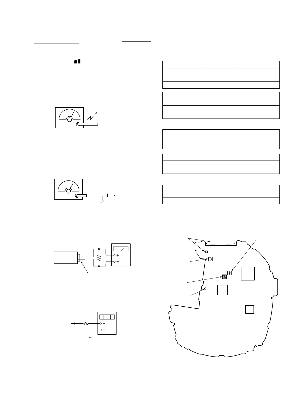
TUNER SECTION
• Switch Location and mode setting
VOLUME : MAX
BASS or BASS
AVLS : OFF
[AM]
BAND: AM
Signal generator
AM RF signal
generator
30% amplitude modulation by 400Hz
signal.
Output level : as low as possible
[FM]
BAND : FM
Signal generator
FM RF signal
generator
75kHz(100%) amplitude modulation
by 1kHz signal.
Output level: as low as possible
: OFF
0 dB = 1 µV
Put the lead-wire
antenna close to
the set.
0.01µF
FM I
point
•Repeat the procedures in each adjustment several times for the
maximum level meter indication.
•The AM tracking adjustments should be finally done by the
trimmer capacitors.
AM FREQUENCY COVERAGE ADJUSTMENT AND CHECK
Adjustment Part Frequency Display
Reading on Digital Voltmeter
Confirmation 530kHz 1.0 ± 0.5V
Confirmation 1710kHz 8.0 ± 0.5V
AM TRACKING ADJUSTMENT
Adjust for a maximum reading on levelmeter
L4 620kHz
CT3 1400kHz
FM FREQUENCY COVERAGE CHECK
Adjustment Part Frequency Display
Reading on Digital Voltmeter
Confirmation 87.5MHz 5.2 ± 0.5V
FM TRACKING ADJUSTMENT
Adjust for a maximum reading levelmeter
L1 98.0MHz
US model only
TV TRACKING ADJUSTMENT
Adjust for a maximum reading on levelmeter
L5 ch10 197.75MHz
Adjustment Location: Main board (Side B)
• Connecting levelmeter
set
J301 (
• Connecting digital voltmeter
TJ8 (VT)
100k
16
Ω
i
)
digital voltmeter
Ω
levelmeter
CT3,L3
AM TRACKING
adjustment
L4
AM FREQUENCY
COVERAGE adjustment
L1
FM TRACKING
adjustment
TJ8(VT)
CT3
L5
L3
TV TRACKING
adjustment
9
D-NF610/NF611
SECTION 5
DIAGRAMS
NOTE FOR PRINTED WIRING BOARDS AND SCHEMATIC DIAGRAMS
Note on Printed Wiring Board
• X : parts extracted from the component side.
• Y : parts extracted from the conductor side.
• : Pattern from the side which enables seeing.
(The other layers' patterns are not indicated.)
Caution:
Pattern face side: Parts on the pattern f ace side seen from
(Side A) the pattern face are indicated.
Parts face side: Parts on the parts face side seen from
(Side B) the parts face are indicated.
• MAIN board is multi-layer printed board. However, the patterns of intermediate-layer have not been included in the diagram.
Note on Schematic Diagram:
• All capacitors are in µF unless otherwise noted. pF: µµF 50 WV
or less are not indicated except for electrolytics and tantalums.
• All resistors are in Ω and 1/
fied.
•%: indicates tolerance.
• C : panel designation.
Note:
The components identified by
mark 0 or dotted line with mark
0 are critical for safety.
Replace only with part number
specified.
• A : B+ Line.
•Total current is measured with CD installed.
•Power voltage is dc 4.5 V and fed with regulated dc power supply
from DC IN jack (J401).
•Voltages and wavef orms are dc with respect to ground in playback
mode.
•Voltages are taken with a VOM (Input impedance 10 MΩ).
Voltage v ariations ma y be noted due to normal production tolerances.
•Waveforms are taken with a oscilloscope.
Voltage v ariations ma y be noted due to normal production tolerances.
• Circled numbers refer to waveforms.
• Signal path.
F : FM
J : CD PLAY (ANALOG OUT)
4
W or less unless otherwise speci-
Note:
Les composants identifiés par
une marque 0 sont critiques
pour la sécurité.
Ne les remplacer que par une
pièce portant le numéro spécifié.
• Waveforms
1 TEST POINT (IC601,if)
600mVp-p
200mV/DIV, 400ns/DIV
5 IC801 wk (XIN)
119ns
1V/DIV, 40ns/DIV
2 IC601 rk (XTAO)
6 IC3 uf (X_O)
2.8Vp-p
59ns
1V/DIV, 40ns/DIV
13.3 µs
500mV/DIV, 4 µs/DIV
2.0Vp-p
1.3Vp-p
✩ When IC803 is damaged, replace the MAIN board.
3 IC403 ef (SYNC)
5.7 µs
1V/DIV, 2 µs/DIV
4 IC701 e; (XTAL)
2.6Vp-p
500mV/DIV, 20ns/DIV
7 Q86 (collector) (FM)
273ns
1V/DIV, 100ns/DIV
3.5Vp-p
44ns
2.8Vp-p
10
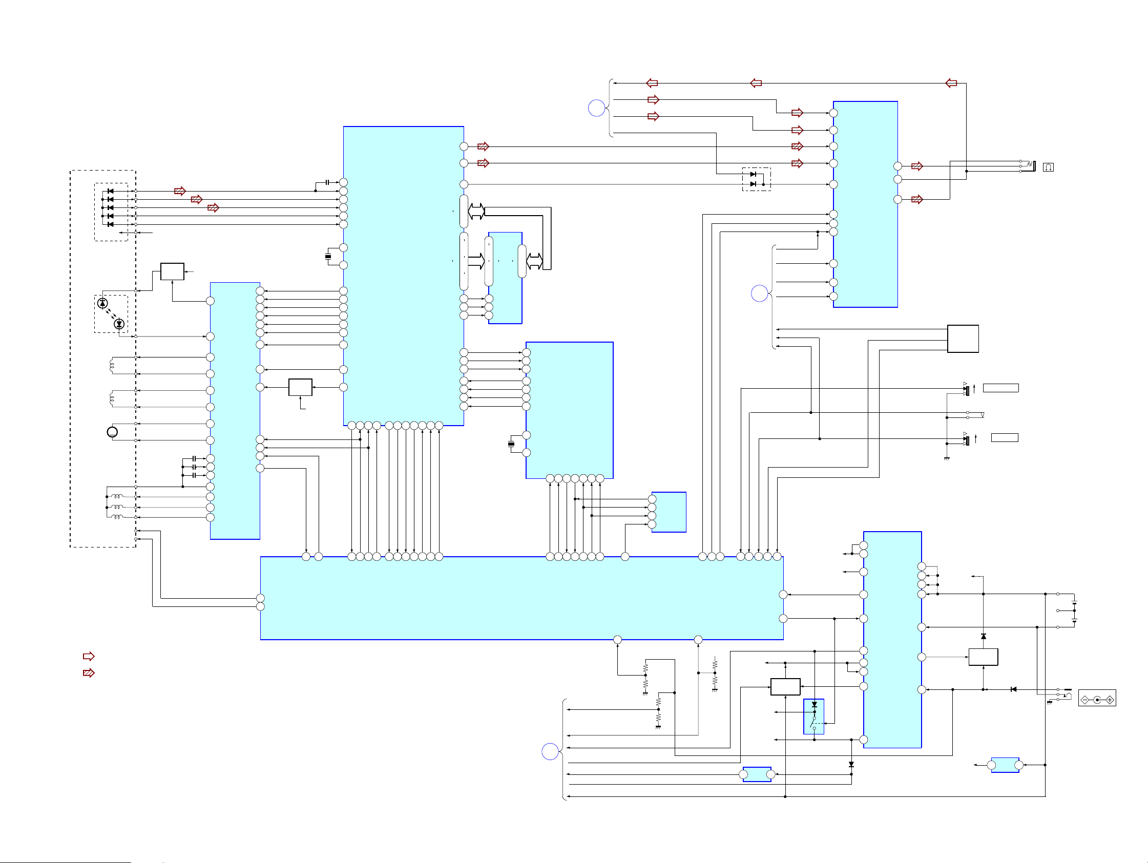
5-1. Block Diagram – MAIN Section –
OPTICAL PICK-UP
DAX-25E
DETECTOR
FOCUS
COIL
TRACKING
COIL
SLED
MOTOR
SPINDLE
MOTOR
• Signal Path
LASER
DIODE
PD
: FM
: CD
VCC
M
LD
OPGSW
OPSTB
RF
A
B
E
F
VCC1_2.25V
LD
PD
F+
F-
T+
T-
S+
S-
COM
U
V
W
Q601
SWITCH
VCC0
31
32
44
42
48
46
52
50
79
78
77
80
2
4
6
IC403(1/2)
COIL/MOTOR
DRIVER
PWG
INM4(PD)
FO3
RO3
FO2
RO2
FO1
RO1
UI
VI
WI
COM
U
V
W
APWM
DATA
CLOK
D-NF610/NF611
FM ANT
HEADPHONE AMP
33
TU-L_I
35
TU-R_I
32
CD-L_I
36
CD-R_I
1
MUTE-SW_I
44
IN-SEL
31
STB_HPSW_I
3
BEEP_I
14
VOL-CTL_I
26
BASS-SW
25
BASS-H/L-SW
IC301
POWER-L_O
CENTER-AMP
POWER-R_O
10
L7
17
VCC1
18
VCC2
RSTB35
19
VCPU
16
VLGO2
20
VCC0
25
STNG
7
6
5
IC403(2/2)
POWER CONTROL
BATM2
DC IN
VD4
VD5
VIN
L5
JOG_PUSH
8
1
5
12
69
62RF1
61
RE1
RE2
S822
JOG
VIN
2
G-PROTECTION
1
OFF
ON
Q402
REG
S811
S820
(OPEN/CLOSE)
S810
HOLD.
D405
D402
J301
DRY BATTRY
SIZE "AA"
(IEC DESIGNATION LR6)
2PCS 3V
J401
DC IN 4.5V
A
PC0
38
18
SDCLK_O
PC3
42
17
SDXLAT_O
TU-L
TU-R
TU MUTE
67
EEP_CS_O
AD_DCINMNT
95
4
3
2
1
IC803
EEPROM
DO
DI
SK
CS
77
56
AUD_SEL_O
AD_BATMNT
92
6
BEEP_O
PWRSW_O
VIN
D309
TU BEEP
TU VOL
TU BASS1
TUNER
SECTION
39
TU_PWRON
37
ESP_I
IC701 AVD
TU BASS2
B
JOG_PUSH
HOLD
OPEN
40
15
14
RE2_I
RE1_I
HOLD_I
LID-SW_I
30
XRESET_I
XWAKE_O 32 WAKEUP37
VCC0
Q403 - 406
+B SWITCH
VCC1_2.25V
VCC2_2.0V
IC702
TUNER
IC601
RF AMP,SERVO,DSP,
D/A CONV,D-RAM CONT
AOUT1
51
AOUT2
56
84
RFAC
88
RFDC
92
A
91
B
89
E
90
F
47
POWLT_O
XTAI
48
XTAO
96
FFDR
95
FRDR
98
TFDR
97
TRDR
100
SFDR
99
SRDR
103
MDP
104
C176
102
MDS
CLOK
XLAT
23
87
XLAT0_O
MSCK0_O
27
86
SCOR
65
52
SCOR_I
FOK
32
28
FOK_I
R8M
XIN
69
53
SENS
22
85
MSDTI0_I
SDTO
21
20
84
83
MSDTO0_O
X601
16.934MHz
60FI3
RI3
59
FI2
58
RI2
57
56FI1
55RI1
73
34SYNC
HG_XSTB_O
HG_GUP_O
Q410
SWITCH
VCC2_2.0V
10
FG_I
90
70XBRK
39
38
40LATCH
FG
74
12
13
GFS
28
GFS_I
XRST
4
XRST_O
XSOE
24
88
XSOE_O
LRMU
PCMD_O
LRCK_O
BCK_O
PCMD_I
LRCK_I
SYSM
25
7
AMUTE_O
D0
D3
A0
A10
XWE
XCAS
XRAS
BCK_I
XRDE
61
4
.
3
.
6
.
5
116
113
.
17
15
.
13
11
.
117
2
9
1
108
106
110
109
107
111
18
IC603
DRAM
9
12
.
A0
15
A10
19
.
21
.
8
4
XWE
23
XCAS
5
XRAS
X701
22MHz
IC801(2/2)
SYSTEM CONTROL
2
.
D0
3
.
D3
24
.
25
4
PCMD
1
LRCK
2
BCK
15
PI0
14
PI2
13
PI3
12
PF4
29
EXTAL
30
XTAL
SECTION
IC701
MP3 DECODER
PF0
NRST
33
34
37
60
66
11
WAKEUP_K_O
AT3_MP3_V_O
PC2
PC1
PF3
40
41
20
19
REQ_I
SDIN_I
SDOUT_O
TU_DCINMNT
TUNER
SECTION
BATMNT
VCPU
C
TU_PWRON
VDD(LCD)
DD_3V
VIN
4.5V
VCC3_2.65V
IC802
+2.4V
REG
11
VCC3
IC806
23
D809
VIN
+1.5V
+1.5V
REG
32
1111
D-NF610/NF611
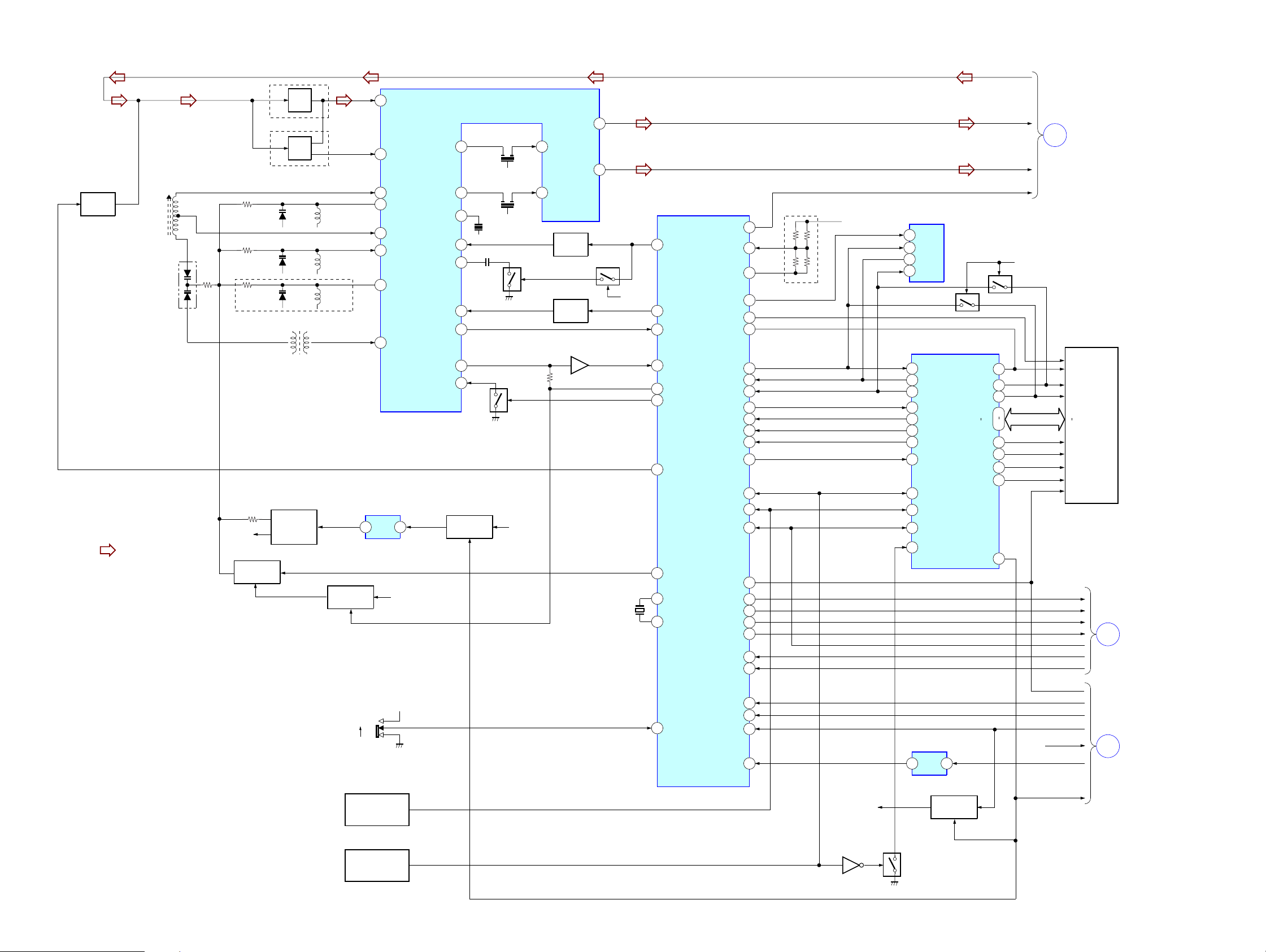
– TUNER Section –
Q3
FM
LOCAL/DX
• Signal Path
AM FERRITE-BAR
: FM
L3
ANTENNA
D3
EXCEPT US
US
DD_3V
Q84, 85
LPF
FL2
B.P.F
US
FL1
B.P.F
D1
D2
D5
AM OSC
T81,Q86 - 88
DC/DC
CONVERTER
L4
L1
FM RF
TV/FM OSC
TV RF
+B SWITCH
S1
(AM_STEP)
L2
L5
Q40, 41
10kHz
9kHz
FM ANT
4
5
11
21
12
22
23
19
20
Q4,11
IC1
FM /AM
IF/RF AMP
CF2
10.7MHz
450kHz
X1
10.7MHz
Q8
Q2
CF1
V IN
10
8
FM-IF_I
AM-IF_I
BAND
CONTROL
BAND
CONTROL
AD6
AD7
TU MUTE
69
50
51
44
49
54
TU-L
TU-R
VCPU
TU_DCINMNT
DD_3V
A
TU BEEP
TU BASS1
TU BASS2
TU_VOL
JOG_PUSH
HOLD
OPEN
VDD(LCD)
BATMNTT
VCPU
DD_3V
VIN
MAIN
SECTION
CS
A0
D6
D7
D0
CRYSTAL
DISPLAY
D5
RD
VDD
LIQUD
MAIN
B
SECTION
MAIN
C
SECTION
L_O
16
R_O
15
IC3
DTS MICROCONTROLLER
Q6
Q9
Q7
Q71
AMP
X61
75kHz
TU_VCC
53
BAND-CTRL1-O
52
BAND-CTRL2-O
71
TV/FM/AM_I
64
IF_I
60
+B ON/OFF_O
61
IF-REQ_O
55
MONO/LOCAL-CTR_O
65
EO(D01)_O
75
X_I
74
X_O
21
AM-STEP_I
TUMUTE-O
EEP-CS_O
CS_O
A0_O
CDU-SDO_O
CDU-SDI_I
CDU-SCK_I
ACK-CD_O
LCD-REQ_I
CD-ON_I
RESET_I
TU-ON_O
VLCD
TUBEEP_O
XTU-BASS1-O
XTU-BASS2-O
VOL-PWM_O
TU HOLD_I
XLID-OPEN_I
VDD
AD DC REF
62
35DEST-I
25DESTVSS_O
32
27
26
47
46
48
54
28
39
73
38
42AD-KEY_I
37KEY2
36AD-KEY3_I
77
49
58
59
50
51
29
43BATT-I
44 HIDC-I
72
45
VERSION SETTING
VCPU
IC62
EEPROM
1CS
DI
3
DO
4
SK
2
Q32
IC801(1/2)
SYSTEM CONTROL
22
DTS_SDTI
21
DTS_SDTO
23
DTS_SCK
35
ACKCD_I
16
LCD_REQ_O
55
CDON_O
59
DTS_RST-O
68
TUON_I
96
AD_KEY1
97
AD_KEY2
98
AD_KEY3
WAKE_I
36
TU_POWERON_O
IC81
+1.6V
2
REG
Q31
LCD_A0
AD0
AD5
XRD_O 71
XWR_O 72 WR
LCD-XRST_O 73 RES
P/S_O 61 P/S
3
FM-RF_I
2
FM-MIX_O
TV-RF_I
1
AM-MIX_O
AM_BP
28
FM-RF_O
29
AM-RF_I
27
FM/TVOSC
24
TV-RF_O
30
AMOSC
25
IC82
+1.8V
3
REG
2
VCPU
VCPU
QUAD
MODE1
DET_O
MODE2
OSC_O
IF-COUNT_O
REQ-SW
+B SWITCH
S807, 808, 812-814
FUNCTION
KEY
S8091-806, 809
FUNCTION
KEY
KEY2
KEY1
TU_PWRON
TU_VCC
Q801
Q802
Q5, 10
+B SWITCH
1212
D-NF610/NF611
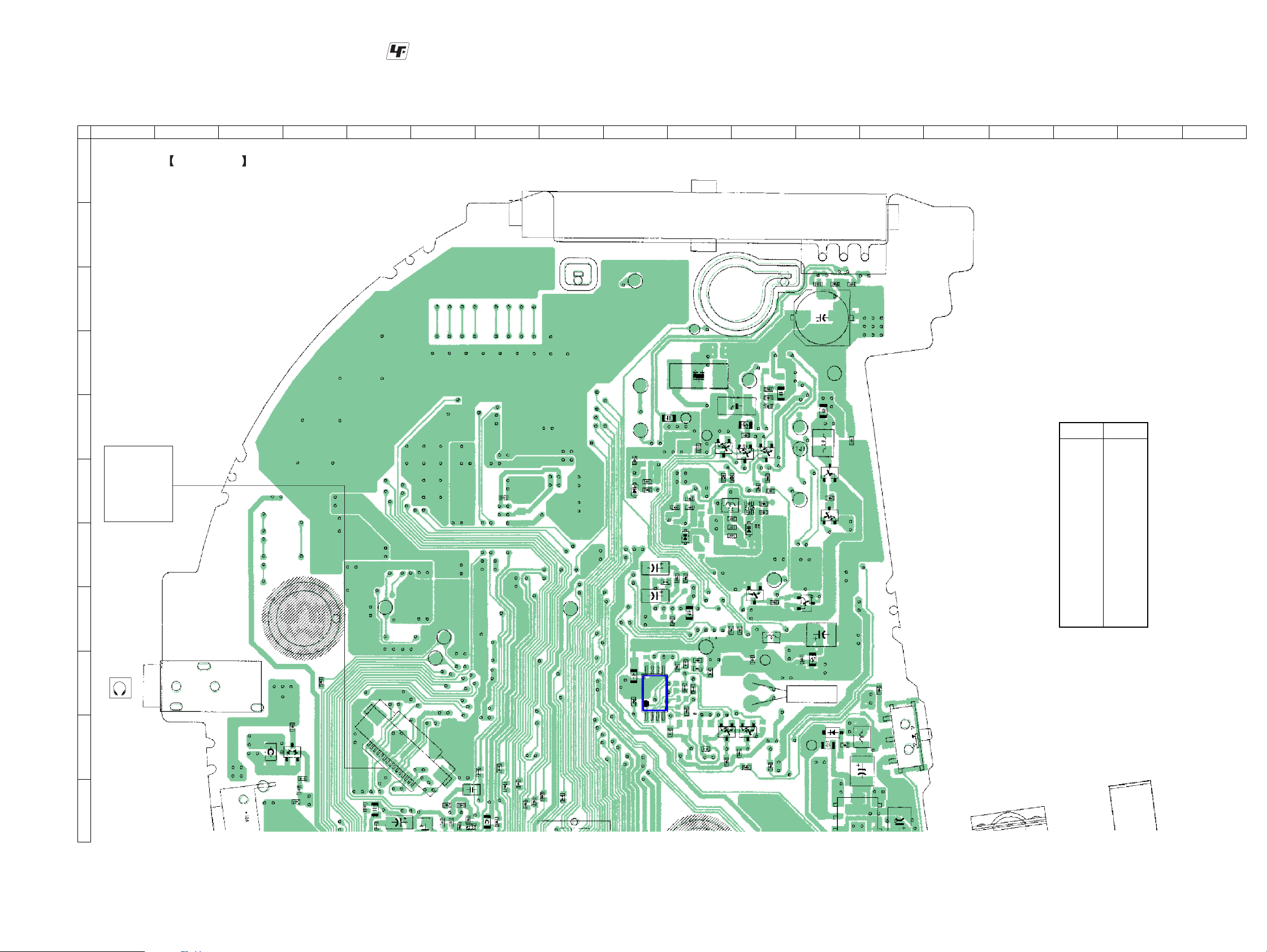
5-2. Printed Wiring Board – MAIN Board (Side A)(1/2) –
1
A
2 3 4 5 6 7 8 9 10 11 12 13 14 15 16 17 18
MAIN BOARD
(SIDE A-1)
B
C
D
E
OPTICAL
PICK-UP
F
BLOCK
DAX-25E
G
H
J301
I
J301
R43
C301
J
FB303
D308
R301
C304
K
S806
C312
• : Uses unleaded solder.
C626
TJ626
TJ2
TJ1
CN601
R101
C107
C324
C322
C302
R328
R110
C334
C315
C313
R307
R306
R304
R201
R717
R104
R730
R713
R714
R715
R915
L3
TJ3
TP15
TJ4
TJ9
C17
C13
D5
TJ6
C92
R62
IC62
CF2
TP2
C20
TP25
C47
R63
R4
C16
C6
D1
R48
R47
C53
C50
TP58
R56
R53
R55
R54
R95
R94
R87
R35
R36
R5
C58
C59
IC62
X1
VDR3
C33
C26
C18
C163
R57
Q32 Q31
R32
C39
L2
R51
R31
TP2
C157
Q6Q7Q2
R18
C9
C160
D2
Q40
R49
C70
R65
R21
R12
R22
C41
R24
C27
R3
C21
TJ80
R40
L62
TP75
C8
C43
TJ24
TJ7
TJ23
Q5
Q41
C69
C71
X61
TP65
C45
R15
LCD
VDR2
C11
R8
TJ22
• Semiconductor
Location
C151
Q10
R23
R151
L81
D81
S1
R88
C94
C91
C55
T81
S1
(AM STEP)
Ref. No. Location
D1 G10
D2 G11
D5 F9
D81 J12
D308 J4
IC62 I9
Q2 E11
Q5 F12
Q6 E11
Q7 E10
Q10 F12
Q40 H11
Q41 H12
Q31 J11
Q32 J10
1313
 Loading...