

Sony DNF-400, DNF-401 Service manual
D-NF400/NF401
SERVICE MANUAL
Ver. 1.3 2005.06
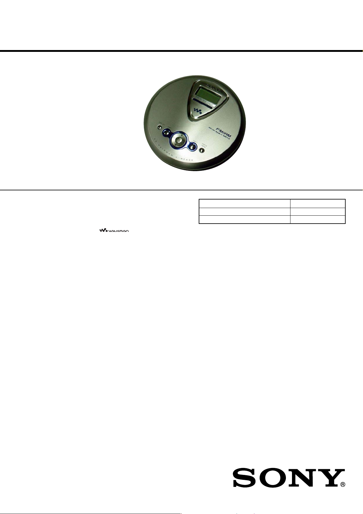
Photo: D-NF400
US and foreign patents licensed from Dolby Laboratories.
•OpenMG, A TRAC, A TRAC3, A TRAC3plus, SonicStage, SonicStage Simple
Burner and their logos aretrademarks of Sony Corporation.
•“WALKMAN” is a registered trademark of Sony Corporation to represent
Headphone Stereo products. is a trademark of Sony Corporation.
• Microsoft, Windo ws, W indows NT ar e trademarks or registered trademarks
of Microsoft Corporation in theUnited States and/or other countries.
• IBM and PC/AT are registered trademarks of International Business Machines Corporation.
• Macintosh is a trademark of Apple Computer , Inc. in the United States and/
or other countries.
•Pentium is a trademark or a registered trademark of Intel Corporation.
• Adobe and Acrobat Reader are trademarks of Adobe Systems Incorporated.
• All other trademarks are trademarks of their respective owners. ™ and ®
marks are omitted in this manual.
US Model
Canadian Model
AEP Model
UK Model
Australian Model
E Model
D-NF400/NF401
Model Name Using Similar Mechanism NEW
CD Mechanism Type CDM-3325ER2
Optical Pick-up Name DAX-25E
SPECIFICATIONS
CD player
System
Compact disc digital audio system
Laser diode properties
Material: GaAlAs
Wavelength: λ = 770 - 800 nm
Emission duration: Continuous
Laser output: Less than 44.6 µW
(This output is the value measured at a distance
of 200 mm from the objective lens surface on
the optical pick-up block with 7 mm aperture.)
D-A conversion
1-bit quartz time-axis control
Frequency response
20 - 20 000 Hz
Output (at 4.5 V input level)
Headphones (stereo minijack)
Approx. 5 mW + Approx. 5 mW at 16 Ω
(Approx. 1.5 mW + Approx. 1.5 mW at 16 Ω)*
*AEP model
+1−2
dB (measured by JEITA)
D-NF400
9-961-446-04 Sony Corporation
2005F05-1 Personal Audio Group
© 2005.06 Published by Sony Engineering Corporation
– Continued on next page –
FM/AM PORTABLE CD PLAYER

D-NF400/NF401
Ver 1.1
Radio
Frequency range
z AEP, UK, EE models
FM: 87.5 - 108.0 MHz
AM: 531 - 1 602 kHz
z E13 (D-NF401), E92 models
•9 kHz step:
FM: 87.5 - 108.0 MHz
AM: 531 - 1 710 kHz
•10 kHz step:
FM: 87.5 - 108.0 MHz
AM: 530 - 1 710 kHz
z E13 (D-NF400), PH, AUS, MX models
•9 kHz step:
FM: 87.5 - 108.0 MHz
AM: 531 - 1 602 kHz
•10 kHz step:
FM: 87.5 - 108.0 MHz
AM: 530 - 1 710 kHz
z US, CND models
•9 kHz step:
TV: 2 - 13 ch
WB (weather band): 1 - 7 ch
FM: 87.5 - 108.0 MHz
AM: 531 - 1 710 kHz
•10 kHz step:
TV: 2 - 13 ch
WB (weather band): 1 - 7 ch
FM: 87.5 - 108.0 MHz
AM: 530 - 1 710 kHz
General
Power requirements
• Two LR6 (size AA) batteries: 1.5 V DC ⋅ 2
• AC power adaptor (DC IN 4.5 V jack):
120 V, 60 Hz (US, CND, E92 and MX models)
240 V, 50 Hz (AUS model)
100 - 240 V, 50/60 Hz (Other models)
Battery life*1 (approx. hours)
When you use the CD player on a flat and stable
surface.
When SOUND mode is set to OFF.
Playing time varies depending on how the CD
player is used.
When using two Sony alkaline batteries
LR6 (SG) (produced in Japan)
G-PROTECTION
“G-PRO 1” “G-PRO 2”
Audio CD 50 45
ATRAC CD*
MP3 CD*
RADIO ON 75
*1 Measured value by the standard of JEITA (Japan
Electronics and Information Technology
Industries Association)
*2 Recorded at 48 kbps
*3 Recorded at 128 kbps
2
3
80 80
62 62
Operating temperature
5°C - 35°C (41°F - 95°F)
Dimensions (w/h/d) (excluding
projecting parts and controls)
Approx. 135.8 × 30.7 × 135.8 mm
3
1
(5
× 1
8
× 5
4
3
in.)
8
Mass (excluding accessories)
Approx. 195 g (6.9 oz.)
Supplied accessories
AC power adaptor (1) (except US, CND models)
Headphones (1) (US model)
Earphones (1) (except US model)
CD-ROM* (SonicStage Simple Burner) (1)
User s guide for SonicStage Simple Burner (1)
* Do not play a CD-ROM on an audio CD player.
Design and specifications are subject to change
without notice.
• Abbreviation
AUS : Australian model
CND: Canadian model
E13 : 220 - 230 V AC area in E model
E92 : 120 V AC area in E model
EE : East European model
MX : Mexican model
PH : Philippines model
Antenna
FM: Headphones/earphones cord antenna
AM: Built-in ferrite bar antenna
SAFETY-RELATED COMPONENT WARNING!!
COMPONENTS IDENTIFIED BY MARK 0 OR DOTTED
LINE WITH MARK 0 ON THE SCHEMATIC DIAGRAMS
AND IN THE PARTS LIST ARE CRITICAL TO SAFE
OPERATION. REPLACE THESE COMPONENTS WITH
SONY PARTS WHOSE PART NUMBERS APPEAR AS
SHOWN IN THIS MANU AL OR IN SUPPLEMENTS PUBLISHED BY SONY.
2
ATTENTION AU COMPOSANT AYANT RAPPORT
À LA SÉCURITÉ!
LES COMPOSANTS IDENTIFIÉS P AR UNE MARQUE 0
SUR LES DIAGRAMMES SCHÉMA TIQUES ET LA LISTE
DES PIÈCES SONT CRITIQUES POUR LA SÉCURITÉ
DE FONCTIONNEMENT. NE REMPLACER CES COMPOSANTS QUE PAR DES PIÈCES SONY DONT LES
NUMÉROS SONT DONNÉS DANS CE MANUEL OU
DANS LES SUPPLÉMENTS PUBLIÉS PAR SONY.

D-NF400/NF401
TABLE OF CONTENTS
1. SERVICING NOTES............................................... 4
2. GENERAL ................................................................... 6
3. DISASSEMBLY
3-1. Disassembly Flow ........................................................... 7
3-2. Cabinet (Lower) Section ................................................. 7
3-3. Optical Pick-up Assy (CDM-3325ER2)......................... 8
3-4. MAIN Board ................................................................... 8
3-5. Liquid Crystal Display Panel (LCD2001),
SWITCH Board............................................................... 9
4. TEST MODE ............................................................... 10
5. ELECTIRICAL CHECK .......................................... 11
6. DIAGRAMS
6-1. Block Diagram – MAIN Section – ................................ 12
6-2. Block Diagram – TUNER Section – ............................. 13
6-3. Note for Printed Wiring Boards and
Schematic Diagrams ....................................................... 14
6-4. Schematic Diagram – MAIN Board (1/7) ..................... 15
6-5. Schematic Diagram – MAIN Board (2/7) ..................... 16
6-6. Schematic Diagram – MAIN Board (3/7) ..................... 17
6-7. Schematic Diagram – MAIN Board (4/7) ..................... 18
6-8. Schematic Diagram – MAIN Board (5/7) ..................... 19
6-9. Schematic Diagram – MAIN Board (6/7) ..................... 20
6-10. Schematic Diagram – MAIN Board (7/7) ..................... 21
6-11. Printed Wiring Board
– MAIN Board (Component Side) – .............................. 22
6-12. Printed Wiring Board
– MAIN Board (Conductor Side) – ................................ 23
6-13. Printed Wiring Board – SWITCH Board – ................... 24
6-14. Schematic Diagram – SWITCH Board – ...................... 25
Notes on chip component replacement
•Never reuse a disconnected chip component.
• Notice that the minus side of a tantalum capacitor may be damaged by heat.
Flexible Circuit Board Repairing
•Keep the temperature of the soldering iron around 270 ˚C during repairing.
• Do not touch the soldering iron on the same conductor of the
circuit board (within 3 times).
• Be careful not to apply force on the conductor when soldering
or unsoldering.
CAUTION
Use of controls or adjustments or performance of procedures
other than those specified herein may result in hazardous radiation exposure.
This appliance is classified as a CLASS 1 LASER product.
The CLASS 1 LASER PRODUCT MARKING is located on
the rear exterior.
About CD-Rs/RWs
This CD player can play CD-Rs/RWs recorded in the ATRAC3plus/
ATRAC3, MP3 or CDDA*format, but playback capability may
vary depending on the quality of the disc and the conditionof the
recording device.
*CDDA is the abbreviation for Compact Disc Digital Audio. It is
a recording standard used for the AudioCDs.
7. EXPLODED VIEWS
7-1. Cabinet (Inner) Section ................................................... 36
7-2. Cabinet (Upper) Section ................................................. 37
7-3. Cabinet (Lower) Section ................................................. 38
7-4. Optical Pick-up Section (CDM-3325ER2)..................... 39
8. ELECTRICAL PARTS LIST ............................... 40
On AC power adaptor
• Use only the AC power adaptor supplied.
If your CD player is not supplied with the
one, use the AC-E45HG AC power
adaptor. Do not use any other AC power
adaptor. It may cause a malfunction.
Polarity of the plug
UNLEADED SOLDER
Boards requiring use of unleaded solder are printed with the leadfree mark (LF) indicating the solder contains no lead.
(Caution: Some printed circuit boards may not come printed with
the lead free mark due to their particular size)
: LEAD FREE MARK
Unleaded solder has the following characteristics.
• Unleaded solder melts at a temperature about 40 ˚C higher than
ordinary solder.
Ordinary soldering irons can be used but the iron tip has to be
applied to the solder joint for a slightly longer time.
Soldering irons using a temperature regulator should be set to
about 350 ˚C.
Caution: The printed pattern (copper foil) may peel away if the
heated tip is applied for too long, so be careful!
• Strong viscosity
Unleaded solder is more viscou-s (sticky, less prone to flow)
than ordinary solder so use caution not to let solder bridges occur such as on IC pins, etc.
• Usable with ordinary solder
It is best to use only unleaded solder but unleaded solder may
also be added to ordinary solder.
3

D-NF400/NF401
SECTION 1
SERVICING NOTES
NOTES ON HANDLING THE OPTICAL PICK-UP
BLOCK OR BASE UNIT
The laser diode in the optical pick-up block may suffer electrostatic breakdown because of the potential difference generated by
the charged electrostatic load, etc. on clothing and the human body .
During repair, pay attention to electrostatic breakdown and also
use the procedure in the printed matter which is included in the
repair parts.
The flexible board is easily damaged and should be handled with
care.
NOTES ON LASER DIODE EMISSION CHECK
The laser beam on this model is concentrated so as to be focused
on the disc reflective surface by the objective lens in the optical
pick-up block. Therefore, when checking the laser diode emission, observe from more than 30 cm away from the objectiv e lens.
• In performing the repair with the power supplied to the set, removing the MAIN board causes the set to be disabled.
In such a case, make a solder bridge to short SL825 (OPEN/
CLOSE DETECT) on the MAIN board in advance.
– MAIN Board (Conductor Side) –
BEFORE REPLACING THE OPTICAL PICK-UP BLOCK
Please be sure to check thoroughly the parameters as par the “Optical Pick-Up Block Checking Procedures” (Part No.: 9-960-027-
11) issued separately before replacing the optical pick-up block.
Note and specifications required to check are given below.
• FOK output: IC601 yg pin
When checking FOK, remove the lead wire to disc motor.
• RF signal P-to-P value: 0.45 to 0.65 Vp-p
LASER DIODE AND FOCUS SEARCH OPERATION
CHECK
During normal operation of the equipment, emission of the laser
diode is prohibited unless the upper lid is closed while turning ON
the S820. (push switch type)
The following checking method for the laser diode is operable.
• Method:
Emission of the laser diode is visually checked.
1. Open the upper lid.
2. W ith a disc not set, turn on the S820 with a screwdri ver having
a thin tip as shown in Fig.1.
3. Push the
4. Observing the objective lens, check that the laser diode emits
light.
When the laser diode does not emit light, automatic power
control circuit or optical pickup is faulty.
In this operation, the objective lens will move up and down 4
times along with inward motion for the focus search.
N X button.
SL825
(OPEN)
detection lever
detection lever
S820
MAIN board
Fig. 1 Method to push the S804
4

System requirements
The following hardware and software specifications are required in order to use the SonicStage
Simple Burner software.
D-NF400/NF401
Computer IBM PC/AT or Compatible
Operating System Factory installed:
Display High Color (16 bit) or higher, 800 × 600 dots or better
Others ¥ Internet access: for Web registration and CDDB* services
¥ CPU: Pentium II 300 MHz or higher (Pentium III 600 MHz or higher is
recommended.)
¥ Hard disk drive space: System folder (on boot disc) — 200 MB or more/
Temporary folder — 200 MB or more (The amount of free space
required differs according to the size of the audio files that you want to
handle. 1.5 GB of free space or more is recommended.)
¥ RAM: 64 MB or more (128 MB or more is recommended)
Others ¥ CD-R/RW drive (capable of digital playback by
Windows XP Home Edition/Windows XP Professional/Windows
Millennium Edition/Windows 2000 Professional/Windows 98 Second
Edition
¥ Adobe Acrobat Reader installed for viewing the PDF manual
WDM)
¥ Sound Board
This software is not supported by the following environments:
¥ NEC PC-98 series or compatible machines, Macintosh systems
¥ Windows XP versions other than Home Edition or Professional
¥ Windows 2000 versions other than Professional
¥ Windows 98 versions other than Second Edition
¥ Windows NT
¥ Windows 95
¥ Personally constructed PCs or operating systems
¥ An environment that is an upgrade of the original manufacturer-installed operating system
¥ Multi-boot environment
¥ Multi-monitor environment
Notes
¥ We do not ensure trouble-free operation on all computers that satisfy the system requirements.
¥ We do not ensure trouble-free operation of the system suspend, sleep, or hibernation function on all
computers.
5
D-NF400/NF401
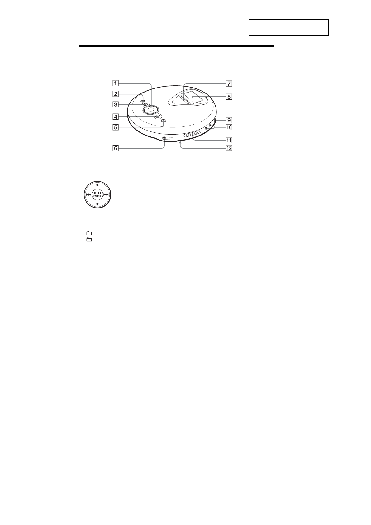
Locating the controls
CD player
SECTION 2
GENERAL
This section is extracted from
instruction manual.
1 Operation button
*1
u
/ENTER: play/pause/
enter
.: AMS
in a preset station
>: AMS/fast forward/
tune in a preset station
V/v
play mode, etc.
2 x (stop)•RADIO OFF button
( group) –•TUNE – button
3
( group) +•TUNE + button
4
5 DISPLAY/MENU button
Use to enter the menu. Also use to enter
the selection as well as u/ENTER.
6 i (headphones) jack
*2
/rewind/tune
: Use to select a file,
7 RADIO ON/BAND•MEMORY button
RADIO ON: Press to turn on the radio.
BAND: Press to change the band.
MEMORY: Press and hold to preset
stations.
8 Display
9 DC IN 4.5 V (external power input) jack
0 VOL (volume) +
qa OPEN switch
Slide the switch to open the CD player
lid.
qs HOLD switch (rear)
Slide the switch in the direction of the
arrow to disable the buttons on the CD
player.
*1 The button has a tactile dot.
*2 Automatic Music Sensor
*1
/– buttons
6
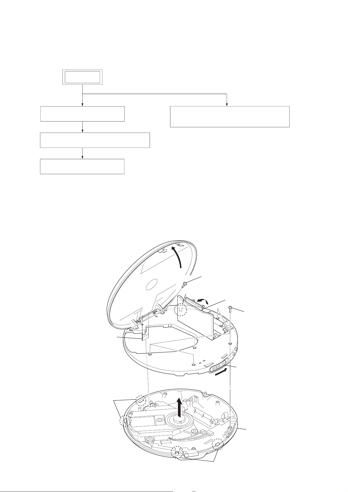
• This set can be disassembled in the order shown below.
3-1. DISASSEMBLY FLOW
SET
D-NF400/NF401
SECTION 3
DISASSEMBLY
3-2. CABINET (LOWER) SECTION
(Page 7)
3-3. OPTICAL PICK-UP ASSY (CDM-3325ER2)
(Page 8)
3-4. MAIN BOARD
(Page 8)
Note: Follow the disassembly procedure in the numerical order given.
3-2. CABINET (LOWER) SECTION
3-5. LIQUID CRYSTAL DISPLAY PANEL (LCD2001),
SWITCH BOARD
(Page 9)
2
two screws
7
flexible flat (20core) cable
(CN801)
5
two claws
6
5
claw
3
Open the battery lid.
4
five screws
1
Open the cabinet (upper) section.
8
cabinet (lower) section
5
two claws
7
D-NF400/NF401
)
3-3. OPTICAL PICK-UP ASSY (CDM-3325ER2)
5
insulator
4
OP flexible board
(CN601)
5
insulator
3
1
spacer
6
optical pick-up assy
(CDM-3325ER2)
2
two connectors
(CN401, CN402
5
insulator
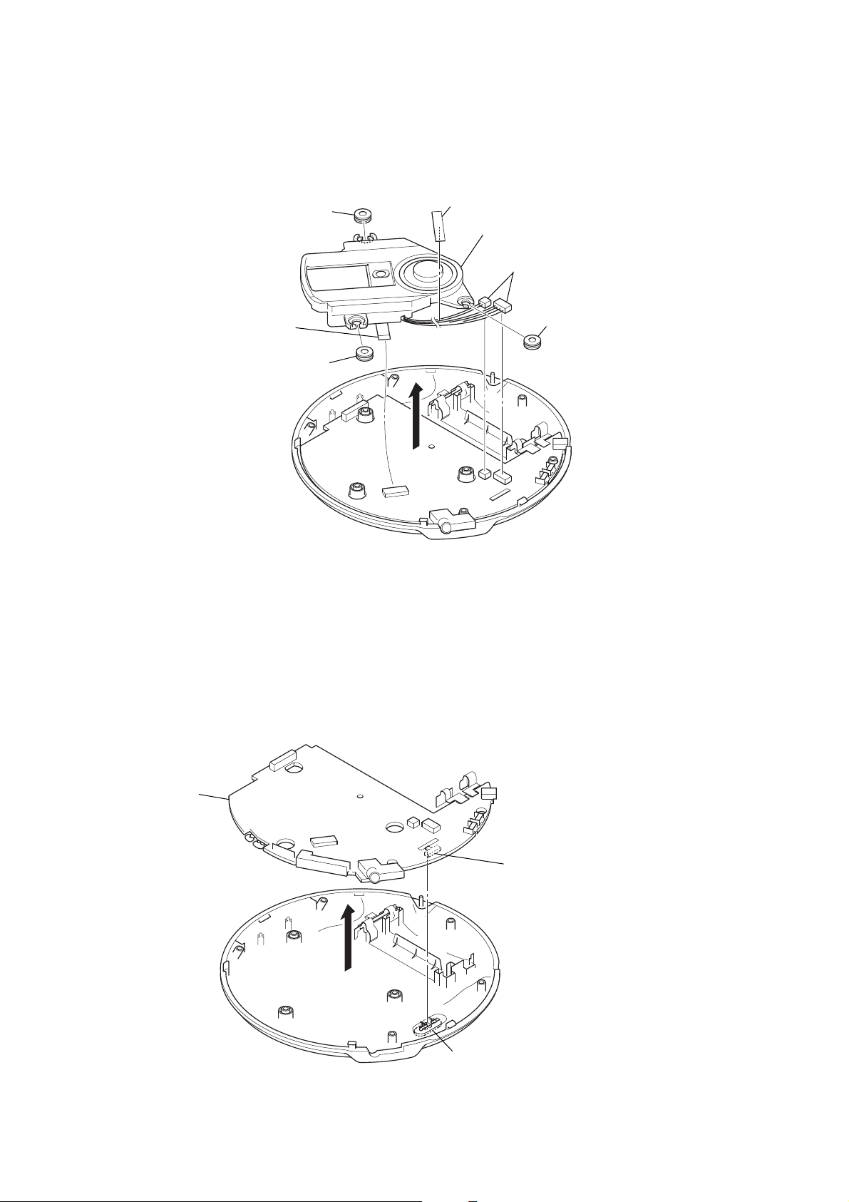
3-4. MAIN BOARD
2
MAIN board
1
S810
Note : On installation of main board,
adjust the position of switch
(S810) and knob (hold).
knob (hold)
8
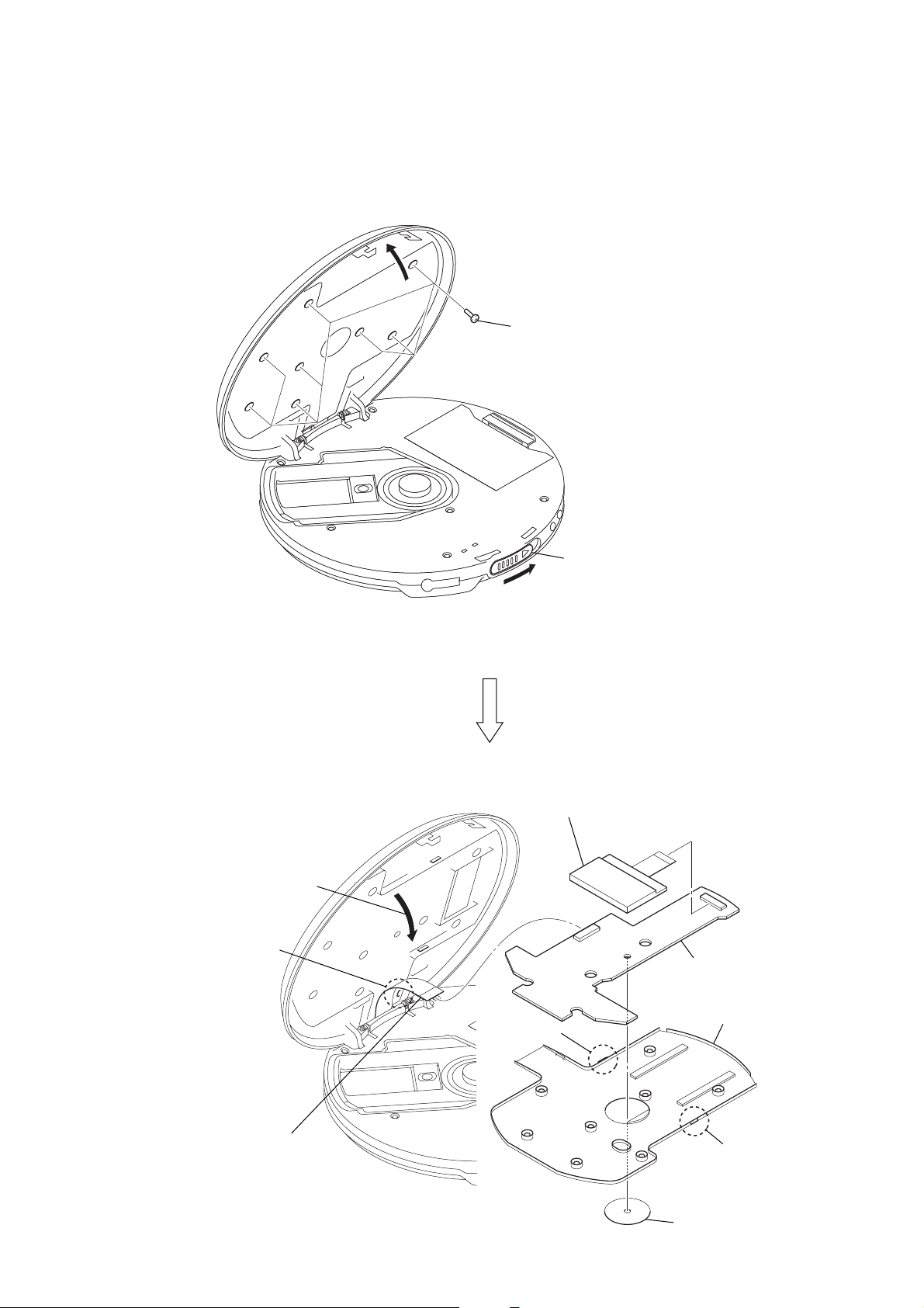
3-5. LIQUID CRYSTAL DISPLAY PANEL (LCD2001), SWITCH BOARD
d
2
eight screws
D-NF400/NF401
4
Open the cover.
3
claw
1
Open the cabinet (upper) section.
6
liquid crystal display panel (LCD2001)
(CN2001)
8
SWITCH boar
5
flexible flat (20core) cable
(CN2002)
3
claw
9
cover
3
claw
7
sheet (color)
9

D-NF400/NF401
SECTION 4
TEST MODE
In the test mode, this set can check the microcomputer version
and liquid crystal display.
1) Short SL824 (TEST) on the MAIN board with a solder bridge.
Then, turn on the power.
2) microcomputer version is displayed on the liquid crystal display, and the liquid crystal display is all lighted.
3) turn off the power and open the solder bridge on SL824 (TEST)
on the MAIN board.
Note: Remove the solders completely. Remaining could be shorted with
the chassis, etc.
– MAIN Board (Conductor Side) –
SL824
(TEST)
10
SECTION 5
p
r
FM RF signal
generator
22.5 kHz frequency
deviation by 400 Hz
signal
Output level: as low as possible
+
–
level meter
set
32
Ω
0.01 µF
MAIN board
TP (FM ANT)
MAIN board
i
jack (J301)
ELECTRICAL CHECK
D-NF400/NF401
CD SECTION
The CD section adjustments are done automatically in this set.
In case of operation check, confirm that focus bias.
Precautions for Check
1. Perform check in the order given.
2. Use YEDS-18 disc (Part No.: 3-702-101-01) unless otherwise
indicated.
3. Power supply voltage requirement: DC4.5 V in DC IN jack.
(J401)
HOLD switch : OFF
Connecting and Checking Location:
– MAIN Board (Conductor Side) –
Focus Bias Check
Condition:
• Hold the set in horizontal state.
Connection:
MAIN board
TP601 (RF)
TP498 (MAIN_GND)
2 k
Ω
oscilloscope
(AC range)
+
–
Procedure:
1. Connect the oscilloscope to the test points TP601 (RF) and
TP498 (GND) on the MAIN board.
2. Set a disc. (YEDS-18)
3. Push the
N X button.
4. Check the oscilloscope waveform is as shown below.
A good eye pattern means that the diamond shape (◊) in the
center of the waveform can be clearly distinguished.
RF Signal reference Waveform (Eye Pattern)
VOLT/DIV : 100 mV (With the 10:1 probe in use)
TIME/DIV : 500 ns
TUNER SECTION 0 dB=1 µV
[AM]
Setting:
Band switch: AM
AM RF signal
generator
30% amplitude
modulation by
400 Hz signal
Output level: as low as possible
[FM]
Setting:
Band switch: FM
Put the lead-wire
antenna close to
the set.
set
level mete
32
Ω
MAIN board
i
jack (J301)
( ): AEP, UK, East European, E, Australian Models
AM FREQUENCY COVERAGE CONFIRMATION
Adjustment Part Frequency Display Reading on Digital Voltmeter
Confirmation 530 (531) kHz 1.0 ± 0.5 V
Confirmation 1,710 (1,602) kHz 7.3 ± 1.0 (6.8 ± 1.0) V
AM TRACKING ADJUSTMENT
Adjust for a maximum reading on level meter
+
–
L3 620 kHz
CT3 1400 kHz
( ): AEP, UK, East European, E, Australian Models
FM FREQUENCY COVERAGE CONFIRMATION
Adjustment Part Frequency Display Reading on Digital Voltmeter
Confirmation 87.5 (108.0) MHz 5.1 ± 0.5 (8.7 ± 0.5) V
FM TRACKING ADJUSTMENT
Adjust for a maximum reading on level meter
L1 98.0 MHz
TV TRACKING ADJUSTMENT
Adjust for a maximum reading on level meter
L5 ch10/97.75 MHz
(D-NF400: US, Canadian models only)
TP498
(MAIN_GND)
TP601
(RF)
RF level
0.45 to 0.65 Vp-
To watch the eye pattern, set the oscilloscope to AC range and
increase the vertical sensitivity of the oscilloscope for easy watching.
5. Stop revolving of the disc motor by pressing the x button.
digital voltmeter
MAIN board
TP8 (VT)
TP498 (MAIN_GND)
100 k
Ω
•Repeat the procedures in each adjustment several times, and the
frequency coverage and tracking adjustments should be finally
done by the trimmer capacitors.
– MAIN Board (Conductor Side) –– MAIN Board (Component Side) –
TP8
(VT)
L1 FM Tracking
L3
AM T rac king
CT3
Adjustment
TP428
(MAIN_GND)
Adjustment
L5 TV T rac king
Adjustment
D-NF400: US,
Canadian models
1111
D-NF400/NF401
6-1. BLOCK DIAGRAM – MAIN Section –
SECTION 6
DIAGRAMS
OPTICAL PICK-UP BLOCK
DAX-25E
DETECTOR
LASER
DIODE
LD
PD
FOCUS
COIL
TRACKING
COIL
OPSTB
OPGSW
M
M902
(SLED)
V
U
W
M901
(SPINDLE)
• SIGNAL PATH
: CD PLAY
: MP3 PLAY
: FM
FM ANT
TU-L
A
PC0
38
18
SDCLK_O
PC3
42
17
SDXLAT_O
TU-R
TU MUTE
67
EEP_CS_O
AD_DCINMNT
95
4
3
2
1
IC803
EEPROM
DO
DI
SK
CS
77
56
AUD_SEL_O
AD_BATMNT
92
VIN
6
BEEP_O
PWRSW
D320
TU BEEP
TU VOL
TU BASS1
TU BASS2
B
(Page 13)
HOLD
OPEN
40
37
HOLD_I
LID-SW_I
XRESET_I
30
XWAKE_O 32 WAKEUP37
VCPU
AVD
CD DSP
IC601
AOUT1
51
AOUT2
56
84
RF
A
B
E
F
X601
12
HG-XSTB_O
13
HG-GUP_O
16.934MHz
10
FG_I
90
LD
PD
F+
F-
T+
T-
S+
S-
COM
U
V
W
AUTOMATIC
POWER
CONTROL
Q601
COIL/MOTOR DRIVE
IC403(1/2)
31
PWG
32
INM4
FO3
RO3
FO2
RO2
FO1
RO1
UI
VI
WI
COM
U
V
W
APWM
DATA
CLOK
44
42
48
46
52
50
79
78
77
80
2
4
6
60FI3
RI3
59
FI2
58
RI2
57
56FI1
55RI1
73
34SYNC
70XBRK
39
38
40LATCH
FG
74
RFAC
88
RFDC
92
A
91
B
89
E
90
F
47
XTAI
48
XTAO
96
FFDR
95
FRDR
98
TFDR
97
TRDR
100
SFDR
99
SRDR
103
MDP
104
C176
102
MDS
SENS
CLOK
XLAT
SDTO
21
20
23
22
83
87
85
XLAT0_O
MSDTI0_I
PWRLAT_O84MSDTO0_O
MSCK0_O
27
86
SCOR_I
SCOR
65
52
FOK
32
28
FOK_I
R8M
XIN
69
53
GFS
28
GFS_I
XRST
4
XRST_O
XSOE
24
88
XSOE_O
LRMU
PCMD_O
LRCK_O
BCK_O
PCMD_I
LRCK_I
BCK_I
SYSM
25
7
AMUTE_O
D0
D3
A0
A10
XWE
XCAS
XRAS
XRDE
61
4
.
3
.
6
.
5
116
113
.
17
15
.
13
11
.
117
2
9
1
108
106
110
109
107
111
18
D-RAM
IC603
2
.
D0
3
.
D3
24
.
25
9
12
.
A0
15
A10
19
.
21
.
8
4
XWE
23
XCAS
5
XRAS
4
1
2
15
14
13
12
X701
22MHz
SYSTEM CONTROLLER
29
30
IC801(1/2)
PCMD
LRCK
BCK
PI0
PI2
PI3
PF4
EXTAL
XTAL
33
60
MP3 DECODER
IC701
PF0
NRST
PC1
PF3
34
37
40
66
11
20
REQ_I
SDIN_I
XKRESET
WAKEUP_K_O
TU_DCINMNT
(Page 13)
PC2
41
19
SDOUT_O
INPUT SELECT, ELECTRICAL VOLUME
33
TU-L_I
35
TU-R_I
32
CD-L_I
36
CD-R_I
1
MUTE-SW_I
44
IN-SEL
31
STB_HPSW_I
3
BEEP_I
14
VOL-CTL_I
26
BASS-SW
25
BASS-H/L-SW
VCC1
VCC2
SL801
VCC0
IC702
IC302
POWER-L_O
CENTER-AMP
POWER-R_O
10
L7
17
VCC1
18
VCC2
RSTB35
19
VCPU
16
VLGO2
20
VCC0
7
6
5
IC403(2/2)
POWER CONTROL
L5
VD4
VD5
VIN
BATM2
DC IN
(OPEN/CLOSE DETECT)
8
1
5
12
69
62RF1
61
S820
J301
ON
S810
HOLD.
OFF
VIN
DRY BATTRY
SIZE "AA"
(IEC DESIGNATION LR6)
2PCS 3V
D401
RIPPLE
FILTER
Q408
D402
J401
DC IN 4.5V
C
(Page 13)
BATMNT
4.5V
VCC3
11
VCC3
+1.4V
+1.4V
REGULATOR
IC806
VCPU
1212
6-2. BLOCK DIAGRAM – TUNER Section –
D-NF400/NF401
Ver 1.1
FM ANT
AM FERRITE-BAR
Q3
NF400 : US, CND/
NF401 : E92, MX
• SIGNAL PATH
: FM
: AM
Abbreviation
AUS : Australian model
CND : Canadian model
E13 : 220-230 V AC area in E model
E92 :120 V AC area in E model
EE : East European model
MX : Mexican model
PH : Philippines model
CT3, L3
AM TRACKING
L3
ANTENNA
D3
CT3
D1
D2
D5
(NF400 : US, CND)
NF400 : AEP, UK, EE, E13, PH, AUS/
NF401 : E13
DC/DC
CONVERTER
Q86, T81
LOW-PASS
FILTER
Q84, 85
FL1
BPF
FM RF
TV/FM OSC
L4
AM OSC
(NF400 : US, CND)
L1
FM TRACKING
L2
L5
TV RF
TV TRACKING
B+ SWITCH
Q40, 41
2
1
28
29
27
24
30
25
14
FM-RF_I
TV-RF_I
AM_BP
FM-RF_O
AM-RF_I
FM/TVOSC
TV-RF_O
AMOSC
LPF
VCPU
FM RF AMP, FM/AM MIX AMP, FM/AM OSC,
FM-MIX_O
AM-MIX_O
QUAD
MODE1
DET_O
MODE2
OSC_O
IF-COUNT_O
REQ-SW
FM/AM IF AMP, FM/AM DET, MPX
4
5
11
21
12
22
23
19
20
B+ SWITCH
Q4,11
IC1
CF2
CF1
X1
Q8
V IN
10
8
FM-IF_I
AM-IF_I
Q71
L_O
R_O
16
TU-L
A
(Page 12)
15
X61
75kHz
DTS MICRO CONTROLLER
IC3
TUMUTE-O
53
BAND-CTRL1-O
23
RE1
52
BAND-CTRL2-O
71
TV/FM/AM_I
64
IF_I
CDU-SDO_O
60
+B ON/OFF_O
61
IF-REQ_O
MONO/LOCAL-
55
CTR_O
65
EO(D01)_O
75
X_I
74
X_O
CDU-SDI_I
CDU-SCK_I
ACK-CD_O
LCD-REQ_I
TUBEEP_O
XTU-BASS1-O
XTU-BASS2-O
VOL-PWM_O
TU HOLD_I
XLID-OPEN_I
EEP-CS_O
CS_O
AO_O
CD-ON_I
RESET_I
TU-ON_O
62
32
27
26
47
46
48
54
28
39
73
38
42AD-KEY_I
37KEY2
49
58
59
50
51
29
43BATT-I
44 HIDC-I
EEPROM
IC62
1CS
DI
3
DO
4
SK
2
SYSTEM CONTROLLER
IC801(2/2)
22
DTS_SDTI
21
DTS_SDTO
23
DTS_SCK
35
ACKCD_I
16
LCDREQ_O
55
CDON_O
59
DTS_RST-O
68
TUON_I
LCD-XRST_O 73 RES
96
AD_KEY1
97
AD_KEY2
WAKE_I
36
TU_POWERON_O
LCD_AO
AD0
AD5
XRD_O 71
XWR_O 72 WR
XCS_O
TU-R
TU MUTE
69
50
AD6
51
AD7
44
49
61 PS
VCPU
54
CS
A0
D6
D7
D0
D5
RD
TU BEEP
TU BASS1
TU BASS2
TU_VOL
HOLD
OPEN
BATMNTT
TU_DCINMNT
LIQUD
CRYSTAL
DISPLAY
LCD2001
(Page 12)
(Page 12)
B
C
S2001 - 2005
FUNCTION
KEY
S806, 809, 2007 - 2011
FUNCTION
KEY
KEY2
KEY1
TU_VCC V IN
Q802
B+ SWITCH
Q10, 12
1313

D-NF400/NF401
2.8 Vp-p
118
µ
s
1.0 Vp-p
13.3 µs
Ver 1.1
6-3. NOTE FOR PRINTED WIRING BOARDS AND SCHEMATIC DIAGRAMS
Note on Printed Wiring Board
• X : parts extracted from the component side.
• Y : parts extracted from the conductor side.
z
•
•
• : Pattern from the side which enables seeing.
(The other layers' patterns are not indicated.)
Caution:
Pattern face side: Parts on the pattern face side seen from
(Conductor Side) the pattern face are indicated.
Parts face side: Parts on the parts face side seen from
(Component Side) the parts face are indicated.
: Through hole.
f
: Internal component.
Note on Schematic Diagram:
• All capacitors are in µF unless otherwise noted. pF: µµF
50 WV or less are not indicated except for electrolytics
and tantalums.
• All resistors are in Ω and 1/
specified.
f
•
• C : panel designation.
• A : B+ Line.
• H : adjustment for repair.
•Power voltage is dc 4.5 V and fed with regulated dc power
•Voltages and waveforms are dc with respect to ground in
•Voltages are taken with a VOM (Input impedance 10 MΩ).
•Waveforms are taken with a oscilloscope.
• Circled numbers refer to waveforms.
• Signal path.
• Abbreviation
: Internal component.
Note:
The components identified by mark 0 or dotted
line with mark 0 are critical for safety.
Replace only with part
number specified.
supply from DC IN jack (J401).
no-signal conditions.
no mark : CD PLAY
〈〈 〉〉 : MP3 PLAY
( ): FM
[]: AM
Voltage variations may be noted due to normal production tolerances.
Voltage variations may be noted due to normal production tolerances.
J : CD PLAY
d : MP3 PLAY
F : FM
f : AM
AUS: Australian model
CND : Canadian model
E13 : 220 - 230 V AC area in E model
E92 : 120 V AC area in E model
EE : East European model
MX : Mexican model
PH : Philippines model
: Impossible to measure
∗
4
W or less unless otherwise
Note:
Les composants identifiés par
une marque 0 sont critiques
pour la sécurité.
Ne les remplacer que par une
pièce portant le numéro
spécifié.
•Waveforms
– MAIN Board –
1 IC601 w; (CLOK)
1.9 µs
2 IC601 es (R8M)
119 µs
3 IC601 rk (XTAO)
59
4 IC601 if (RFAC)
6 IC403 ef (SYNC)
2.0 Vp-p
2.1 Vp-p
5.7
7 IC801 wk (XIN)
8 IC3 uf (X_O)
µ
s
2.0 Vp-p
1.4 Vp-p
µ
s
9 Q86 Collector (tuner mode)
5 IC601 <z/v (C176)
5.7 µs
Approx.
600 mVp-p
191 ns
q; IC701 e; (XTAL) (MP3 play mode)
2.0 Vp-p
44.2 ns
3.8 Vp-p
1.6 Vp-p
1414

6-4. SCHEMATIC DIAGRAM – MAIN Board (1/7) – • See page 14 for Waveforms. • See page 29 for IC Pin Function Description.
D-NF400/NF401
CN601
15P
OPGSW
A
B
RF
OPSTB
LD
PD
AGND
VCC
E
F
F+
T-
T+
F-
(1/7)
MDS
FB601
X601
16.934MHz
R611
C621
6.3V
0
CD DSP
CXD3048R
47
IC601
FB402
LRCKO
R612
47
R609
0
L602
47µH
R606
0
A1
A2
A3
C623
PCMDO
LRCKI
PCMDI
0
1
BCKI
BCKO
R8M
FB602
R614
10k
A10
A0
C697
C618
0.1
0.1
VDR603
VDR602
R648
R613
10k
A4
A5
A6
A7
A8
A9
XCAS
D2
D3
D0
D1
XWE
XRAS
22k
C629
0.1
R649
0
XRST
SCOR
R645R643
00
R642
R641
R640
R639
R638
SYSM
XSOE
0
XLAT
0
SENS
0
DATA
0
CLDK
0
C606
1000p
L603
10µH
A0
A1
A2
D-RAM
IC603
MSM51X17400F
-10TFSR1
C622
10
6.3V
VCC
VSS
A3
A3A2A1
A5
A4
A10
A0
A10
A9
A8A7A6A5A4
A8
A7
A6
A9
D0
D1
XWE
XRAS
0
0
647
R644
R
D1
D0
XWE
XRAS
XOE
VCCVSS
D3
D2
XCAS
0
651
R
D3
D2
XCAS
C624
1
C619
22
6.3V
OPGSW
OPSTB
F+
T-
T+
F-
C631
6.3V
C632
L601
Q601
2SB16790
AUTOMATIC
CONTROL
R670
4.7k
POWER
R608
C610
R610
10
100k
6.3V
A
B
RF
E
F
C607
4700p
C608
22
C698
0.1
R646
2.2
47
4V
RF
0
E
F
B
A
FB401
0
R622 R623
TP601
(RF)
R603SL601 R602
22k 22k
SL602
R618
2.2k
C605
0.1
10k
R621
0.47
1M 220k
0.47 10k
C609 R624
100p
C612
470k
R625
R626C613
02200p
R663
100k
22k
R604
22k
R605
C616 C617
470p 470p
FOK
GFS
R619
2.2k
C699C614R629R662R628 R630
0.122p47k47k22k 47k
R632 R633 C601 C611
100k 100k 470p 470p
FFDR
FRDR
TFDR
TRDR
SFDR
SRDR
R607
0
A1
A2
A3
A4
D1
D2
D3
(Page 16)
(Page 21)
C1
10
B1
B2
B3
B4
B5
B6
B7
B8
11
B9
B
B
13
B12
B
(Page 19)
(Page 18)
The components identified by mark 0 or dotted
line with mark 0 are critical for safety.
Replace only with part number specified.
Les composants identifiés par une marque 0 sont
critiques pour la sécurité. Ne les remplacer que
par une pièce portant le numéro spécifié.
1515
 Loading...