

D-NF007/NF0070
SERVICE MANUAL
Ver. 1.1 2005.11
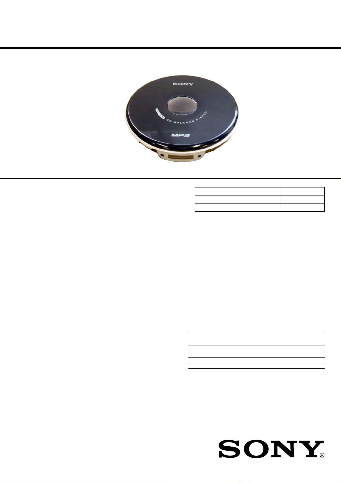
Photo : D-NF007
SPECIFICATIONS
Canadian Model
AEP Model
D-NF007
E Model
D-NF007/NF0070
Australian Model
D-NF007
Model Name Using Similar Mechanism D-FJ003
CD Mechanism Type CDM-3525A
Optical Pick-up Name DAX-25E
CD player
System: Compact disc digital audio system
Laser diode properties:
Emission duration: Continuous
Laser output: Less than 44.6 µW (This output is the value measured at a
distance of 200 mm from the objective lens surface on the optical pick-up
block with 7 mm aperture.)
Radio
Frequency range
• Canadian and Latin American models
9 kHz step:
FM: 87.5 - 108 MHz
AM: 531 - 1 710 kHz
10 kHz step:
FM: 87.5 - 108 MHz
AM: 530 - 1 710 kHz
• Other models
9 kHz step:
FM: 87.5 - 108 MHz
AM: 531 - 1 602 kHz
10 kHz step:
FM: 87.5 - 108 MHz
AM: 530 - 1 710 kHz
Antennas
FM: Headphones cord antenna
AM: Built-in ferrite bar antenna
General
Power requirements:
•Two LR6 (size AA) batteries: 1.5 V DC × 2
• AC power adaptor (DC IN 4.5 V jack):
220 V, 50 Hz (Model for China)
120 V, 60 Hz (Model for Mexico)
Dimensions (w/h/d) (without projecting parts and controls):
Approx. 139.8 × 28.8 × 139.8 mm (5 5⁄8 × 1 3⁄16 × 5 5⁄8 in.)
Mass (excluding accessories):
Approx. 219 g (7.8 oz.)
Operating temperature: 5°C - 35°C (41°F - 95°F)
MPEG Layer-3 audio coding technology and patents licensed from
Fraunhofer IIS and Thomson.
Design and specifications are subject to change without notice.
Supplied accessories
AC power adaptor (1) (not supplied with the USA model)
Headphones (1)
Battery life* (approx. hours)
(When the CD player is used on a flat and stable place.)
Playing time varies depending on how the CD player is used.
When using two Sony alkaline batteries LR6 (SG)
(produced in Japan)
G-PROTECTION G-on G-off
Audio CD 16 11
MP3 CD (Recorded at 128 kbps) 23 23
RADIO ON 35
* Measured value by the standard of JEITA (Japan Electronics and
Information Technology Industries Association).
Design and specifications are subject to change without notice.
FM/AM PORTABLE CD PLAYER
9-879-827-02
2005K02-1
© 2005.11
Sony Corporation
Personal Audio Division
Published by Sony Engineering Corporation

D-NF007/NF0070
TABLE OF CONTENTS
1. SERVICING NOTES ................................................ 3
2. GENERAL ................................................................... 3
3. DISASSEMBLY
3-1. Disassembly Flow ........................................................... 4
3-2. Upper Lid Assy, Cabinet (Middle) Assy,
Cabinet (Lower) Assy...................................................... 4
3-3. Optical Pick-Up (CDM-3525A), Main Board ................. 5
4. ELECTRICAL ADJUSTMENT ............................. 6
5. DIAGRAMS
5-1. Block Diagram – CD/Power Section –........................... 10
5-2. Block Diagram – Tuner Section – .................................. 11
5-3. Printed Wiring Board – Main Board (Side A) – ............. 12
5-4. Printed Wiring Board – Main Board (Side B) – ............. 13
5-5. Schematic Diagram – Main Board (1/3) – ..................... 14
5-6. Schematic Diagram – Main Board (2/3) – ..................... 15
5-7. Schematic Diagram – Main Board (3/3) – ..................... 16
5-8. IC Pin Function Description ............................................ 20
6. EXPLODED VIEWS ................................................. 23
7. ELECTRICAL PARTS LIST .................................. 24
Notes on chip component replacement
• Never reuse a disconnected chip component.
• Notice that the minus side of a tantalum capacitor may be
damaged by heat.
Flexible Circuit Board Repairing
• Keep the temperature of the soldering iron around 270 ˚C
during repairing.
• Do not touch the soldering iron on the same conductor of the
circuit board (within 3 times).
• Be careful not to apply force on the conductor when soldering
or unsoldering.
CAUTION
Use of controls or adjustments or performance of procedures
other than those specified herein may result in hazardous radiation
exposure.
UNLEADED SOLDER
Boards requiring use of unleaded solder are printed with the leadfree mark (LF) indicating the solder contains no lead.
(Caution: Some printed circuit boards may not come printed with
the lead free mark due to their particular size.)
: LEAD FREE MARK
Unleaded solder has the following characteristics.
• Unleaded solder melts at a temperature about 40°C higher than
ordinary solder.
Ordinary soldering irons can be used but the iron tip has to be
applied to the solder joint for a slightly longer time.
Soldering irons using a temperature regulator should be set to
about 350°C.
Caution: The printed pattern (copper foil) may peel away if
the heated tip is applied for too long, so be careful!
• Strong viscosity
Unleaded solder is more viscous (sticky, less prone to flow)
than ordinary solder so use caution not to let solder bridges
occur such as on IC pins, etc.
• Usable with ordinary solder
It is best to use only unleaded solder but unleaded solder may
also be added to ordinary solder.
SAFETY-RELATED COMPONENT WARNING!!
COMPONENTS IDENTIFIED BY MARK 0 OR DOTTED LINE
WITH MARK 0 ON THE SCHEMATIC DIAGRAMS AND IN
THE PARTS LIST ARE CRITICAL TO SAFE OPERATION.
REPLACE THESE COMPONENTS WITH SONY PARTS WHOSE
PART NUMBERS APPEAR AS SHOWN IN THIS MANUAL OR
IN SUPPLEMENTS PUBLISHED BY SONY.
2
ATTENTION AU COMPOSANT AYANT RAPPORT
À LA SÉCURITÉ!
LES COMPOSANTS IDENTIFIÉS PAR UNE MARQUE 0 SUR LES
DIAGRAMMES SCHÉMATIQUES ET LA LISTE DES PIÈCES
SONT CRITIQUES POUR LA SÉCURITÉ DE FONCTIONNEMENT.
NE REMPLACER CES COMPOSANTS QUE PAR DES PIÈCES
SONY DONT LES NUMÉROS SONT DONNÉS DANS CE MANUEL
OU DANS LES SUPPLÉMENTS PUBLIÉS PAR SONY.
SECTION 1
SERVICING NOTES
D-NF007/NF0070
NOTES ON HANDLING THE OPTICAL PICK-UP
BLOCK OR BASE UNIT
The laser diode in the optical pick-up block may suffer electrostatic
break-down because of the potential difference generated by the
charged electrostatic load, etc. on clothing and the human body.
During repair, pay attention to electrostatic break-down and also
use the procedure in the printed matter which is included in the
repair parts.
The flexible board is easily damaged and should be handled with
care.
NOTES ON LASER DIODE EMISSION CHECK
The laser beam on this model is concentrated so as to be focused on
the disc reflective surface by the objective lens in the optical pickup block. Therefore, when checking the laser diode emission,
observe from more than 30 cm away from the objective lens.
LASER DIODE AND FOCUS SEARCH OPERATION
CHECK
During normal operation of the equipment, emission of the laser
diode is prohibited unless the upper lid is closed while turning ON
the S811. (push switch type)
The following checking method for the laser diode is operable.
• Method:
Emission of the laser diode is visually checked.
1. Open the upper lid.
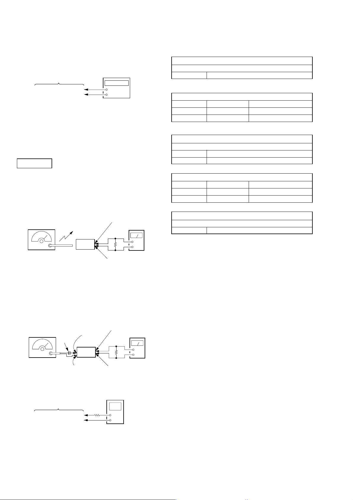
2. With a disc not set, turn on the S811 with a screwdriver having
a thin tip as shown in Fig.1.
3. Press the u button.
4. Observing the objective lens, check that the laser diode emits
light.
When the laser diode does not emit light, automatic power
control circuit or optical pick-up is faulty.
In this operation, the objective lens will move up and down 2
times along with inward motion for the focus search.
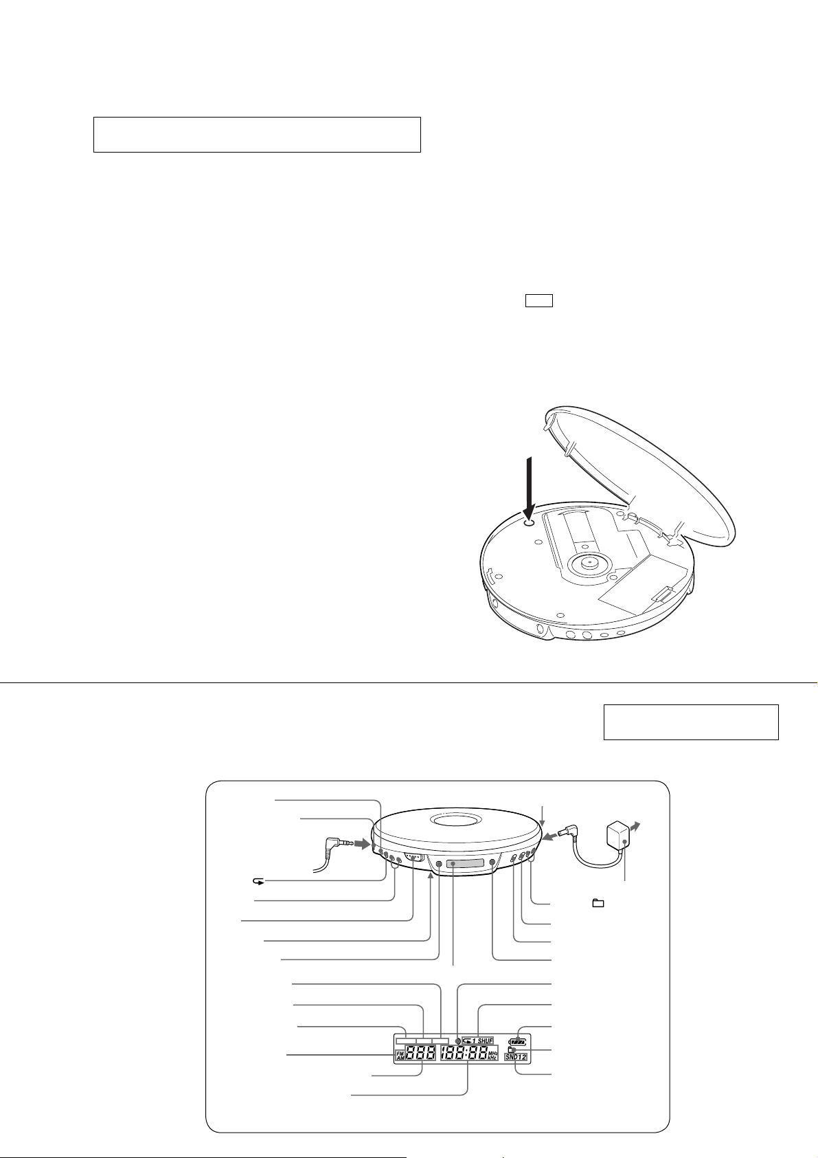
S811
LOCATING THE CONTROLS
SOUND/AVLS
i (headphones) jack
P MODE/
VOL +*/–
OPEN
HOLD (rear)
RADIO ON/BAND
* The button has a tactile dot.
Headphones
MONO
LOCAL
PRESET
Band
Track number/Preset number
Playing time/Frequency
SECTION 2
GENERAL
Display
PRESET LOCAL MONO
Fig. 1 Method to push the S811
This section is extracted from
instruction manual.
DC IN 4.5 V
to an AC outlet
AC power adaptor
./>•
TUNE –/+
u*(play/pause)/ENTER
x (stop)•RADIO OFF
GROUP
MP3 indicator
Play mode
Remaining battery power
Group indicator
Sound mode
(group) –/+ •
3
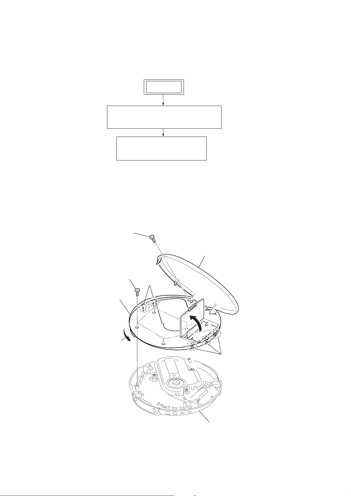
D-NF007/NF0070
• This set can be disassembled in the order shown below.
3-1. DISASSEMBLY FLOW
3-2. UPPER LID ASSY, CABINET (MIDDLE) ASSY, CABINET (LOWER) ASSY
(Page 4)
3-3. OPTICAL PICK-UP (CDM-3525A),
MAIN BOARD
(Page 5)
SECTION 3
DISASSEMBLY
SET
Note: Follow the disassembly procedure in the numerical order given.
3-2. UPPER LID ASSY, CABINET (MIDDLE) ASSY, CABINET (LOWER) ASSY
4
screw
upper lid assy
3
five screws
5
two claws
cabinet (middle) assy
2
1
open
6
three claws
cabinet (lower) assy
4
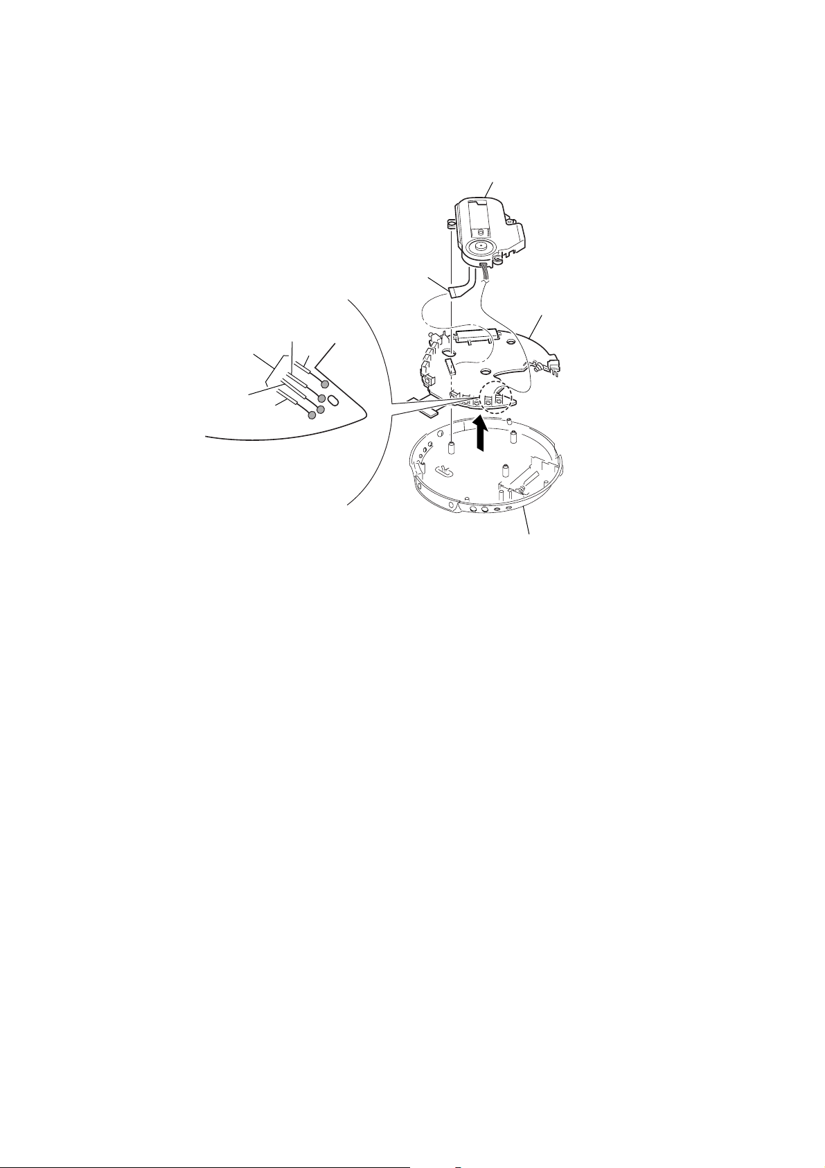
3-3. OPTICAL PICK-UP (CDM-3525A), MAIN BOARD
A
1
CN501
3
Unsolder four lead wires
4
optical pick-up CDM-3525
5
MAIN board
D-NF007/NF0070
to optical pick-up
BLK
RED
MAIN board (side A)
GRY
ORG
2
cabinet (lower) assy
5
D-NF007/NF0070
Ver. 1.1
SECTION 4
ELECTRICAL ADJUSTMENTS
[TUNER SECTION]
CLOCK SHIFT ADJUSTMENT
Connection:
MAIN board
TP471 (SIFT)
TP005 (RFGND (A)) or
TP003 (RFGND (B))
frequency counter
+
–
Adjusting Procedure:
1. Connect the frequency counter to TP471 (SIFT) and TP005
(RFGND (A)) or TP003 (RFGND (B)) on the MAIN board.
2. Set the AM 621 kHz (9kHz step model) or AM 620 kHz
(10kHz step model)
3. Adjust the RV471 so that the reading of frequency counter is
180 ± 1 kHz.
0 dB=1 µV
[AM]
Setting:
Function: RADIO
Band: AM
AVLS: OFF
MAIN board
AM RF signal
generator
30% amplitude
modulation by
400 Hz signal
Output level:
as low as possible
Put the lead-wire
antenna close to
the set.
TP012 (TU_L) or
TP014 (TU_R)
32
Ω
set
MAIN board
TP005 (RFGND (A)) or
TP003 (RFGND (B))
level meter
+
–
( ): 9kHz step model
AM IF ADJUSTMENT
Adjust for a maximum reading on level meter
T002 620 (621) kHz
( ): 9kHz step model
AM FREQUENCY COVERAGE CONFIRMATION
Adjustment Part Frequency Display Reading in Digital Voltmeter
Confirmation 530 (531) kHz 0.8 ± 0.5 V
Confirmation 1,710 (1,602) kHz 7.2 (6.8) ± 1.0 V
( ): 9kHz step model
AM TRACKING ADJUSTMENT
Adjust for a maximum reading on level meter
T001 620 (621) kHz
CT001 1,400 (1,404) kHz
FM FREQUENCY COVERAGE ADJUSTMENT
Adjustment Part Frequency Display Reading in Digital Voltmeter
Confirmation 87.5 MHz 2.8 ± 1.0 V
L004 108 MHz 8.0 ± 1.0 V
FM TRACKING ADJUSTMENT
Adjust for a maximum reading on level meter
L003 98 MHz
Adjustment and Connecting Location: MAIN board
(See page 7)
[FM]
Setting:
Function: RADIO
Band: FM
AVLS: OFF
MAIN board
TP012 (TU_L) or
TP014 (TU_R)
level meter
32
Ω
MAIN board
TP005 (RFGND (A)) or
TP003 (RFGND (B))
digital voltmeter
Ω
+
–
FM RF signal
generator
0.01 µF
33.75 kHz frequency
deviation by 1 kHz
signal
Output level:
as low as possible
TP005 (RFGND (A)) or
TP003 (RFGND (B))
TP005 (RFGND (A)) or
MAIN board
TP006 (VT)
MAIN board
TP002 (RF (A)) or
TP001 (RF (B))
set
MAIN board
TP003 (RFGND (B))
100 k
• Repeat the procedures in each adjustment several times, and
the tracking adjustments should be finally done by the trimmer
capacitors.
6
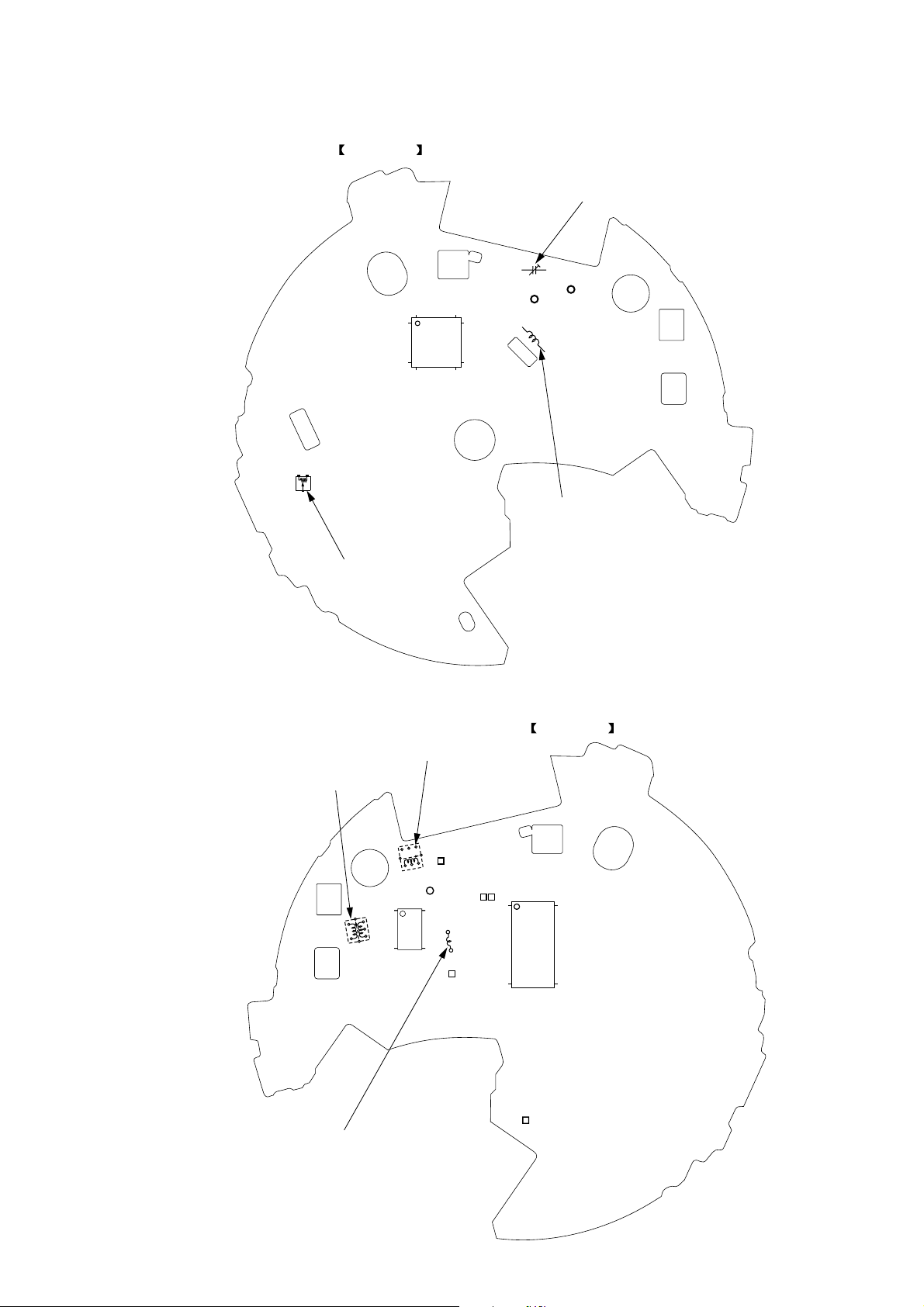
Adjustment and Connecting Location:
D-NF007/NF0070
(SIDE A)MAIN BOARD
CT001:
AM Tracking Adjustment
RV471:
Clock Shift Adjustment
T002:
AM IF Adjustment
TP005
80
1
IC601
20
21
(RFGND(A))
61
60
41
40
T001:
AM Tracking Adjustment
TP001
(RF(B))
L003:
FM Tracking Adjustment
MAIN BOARD
(SIDE B)
TP002
T001
(RF(A))
TP003
(RFGND(B))
1
IC001
15
30
16
TP012
(TUL)
TP006
(VT)
L004:
FM Frequency Coverage Adjustment
TP014
(TUR)
1
25
TP471
(SIFT)
50
IC602
26
7
D-NF007/NF0070
R601
1
0
)
Ver. 1.1
[CD SECTION]
The CD section adjustments are done automatically in this set.
Adjusting Procedure:
1. Perform check in the order given.
2. Use YEDS-18 disc (Part No: 3-702-101-01) unless otherwise
indicated.
3. Power supply voltage requirement :DC4.5 V in DC IN jack.
(J401)
VOLUME button : Minimum
HOLD switch :OFF
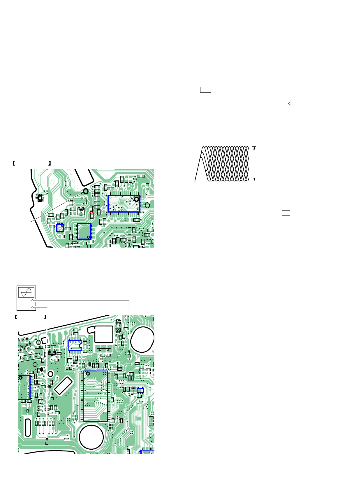
Focus bias Check
Condition:
• Hold the set in horizontal state.
Connection:
D871
(SIDE A)
R472
R475
C472
R474
4
C478
5
R411
C474
1
IC471
8
D004
C471
C473
021
SL801
OPEN
R477
(EXCEPT AEP)
R476
R473
C805
Q475
RV471
5
IC802
8
ECB
C040
4
R020
(AEP)
R824
R1015
R1014
R821
R872
R1016
15
16
R1010
IC1001
C001
R871
R873
R826
R828
R812
R808
R804
R844
R843
1
8
MAIN BOARD
SL801(OPEN)
C880
R1011
R1012
C814
R874
R1003
R1019
C812
C806
R1017
1
Procedure:
1. Make a solder bridge to short SL801 (OPEN) on the MAIN
board side A.
2. Connect the oscilloscope to the test point TP604 (RF) and
TP406 (M-GND) on the MAIN board side B.
3. Set a disc. (YEDS-18)
4. Press the u button.
5. Check the oscilloscope waveform is as shown below.
A good eye pattern means that the diamond shape (
) in the
center of the waveform can be clearly distinguished.
RF Signal reference Waveform (Eye Pattern)
VOLT/DIV : 500 mV (With the 10 : 1 probe in use
TIME/DIV : 500ns
RF level
±
0.2 Vp-p
1.2
R1018
To watch the eye pattern, set the oscilloscope to AC range and
increase the vertical sensitivity of the oscilloscope for easy
watch-ing.
SL871
30
6. Stop revolving of the disc motor by pressing the x button.
7. SL801 is opened by taking the solder bridge.
R876
C874
ECB
C877
Q804
2
oscilloscope
(AC range)
+
–
MAIN BOARD
(SIDE B)
1
TAP001
C014
TP002
RF(A)
FL001
TAP003
RF GND(B)
C023
30
IC001
16
5
C043C045
X001
TP406
M-GND
TP604(RF)
TP406(M-GND)
NATURAL
GREEN
RED
C022
R004
C003
C002
R001
C024
C005
D001
R002
C006
D002
C011
C020
C018
R007
C021
C037
R109
G
D
S
L005
C046
R013
R018
TP012
TUL
C102
D003
C109
TP013
GND
C031
R014
C035
C032
R016
TP006
VT
R220
R024
R012
R011
8
9
RB901
TP014
TUR
IC901
R906
R902
R901
R1008
C910
R1009
FB901
Q102
C301
Q101
R303
C620
50
TP604
C635
R617
C627
FB604
FB605
R204
R203
R103
C109
C209
RF
C631
R626
R621
C626
R632
R606
C612
C606
C605
FB606
C632
C633
C634
R627
1
C905
C906
X601
R902
C907
16
R905
R618 R622
FB601
C638
R904
C624
1
IC602
25
26
1004
IC603
5
1
R630
41
FB201
R620
R615
C615
R613
C609
4
3
R605
R604
R603
IC
40
8
SECTION 5
DIAGRAMS
D-NF007/NF0070
• Note for Printed Wiring Boards and Schematic Diagrams
Note on Printed Wiring Boards.
• X : parts extracted from the component side.
• Y : parts extracted from the conductor side.
• a : Through hole.
• f : internal component
• : Pattern from the side which enables seeing.
(The other layers' patterns are not indicated.)
Caution:
Pattern face side: Parts on the pattern face side seen from
(Side B) the pattern face are indicated.
Parts face side: Parts on the parts face side seen from
(Side A) the parts face are indicated.
• Abbreviation
3AEP : UK model
8E19 : Philippines model
AUS : Australian model
CND : Canadian model
E19 : Singapore model
EE : East European model
Note on Schematic Diagrams.
• All capacitors are in µF unless otherwise noted. (p: pF)
50 WV or less are not indicated except for electrolytics
and tantalums.
• All resistors are in Ω and 1/
specified.
• f : internal tolerance.
• C : panel designation.
Note:
The components identified
by mark 0 or dotted line
with mark 0 are critical for
safety.
Replace only with part
number specified.
• A : B+ Line.
• H : adjustment for repair.
• Power voltage is dc 3 V and fed with regulated dc power
supply from battery terminal.
•Voltages and waveforms are dc with respect to ground
under no-signal (detuned) conditions.
no mark : CD PLAY
( ) : FM
[ ] : AM
•Voltages are taken with a VOM (Input impedance 10 MΩ).
Voltage variations may be noted due to normal production tolerances.
•Waveforms are taken with a oscilloscope.
Voltage variations may be noted due to normal production tolerances.
• Circled numbers refer to waveforms.
• Signal path.
J : CD PLAY
F : FM
f : AM
• Abbreviation
3AEP : UK model
8E19 : Philippines model
AUS : Australian model
CND : Canadian model
E19 : Singapore model
EE : East European model
4
W or less unless otherwise
Note:
Les composants identifiés
par une marque 0 sont
critiques pour la sécurité.
Ne les remplacer que par une
piéce portant le numéro
spécifié.
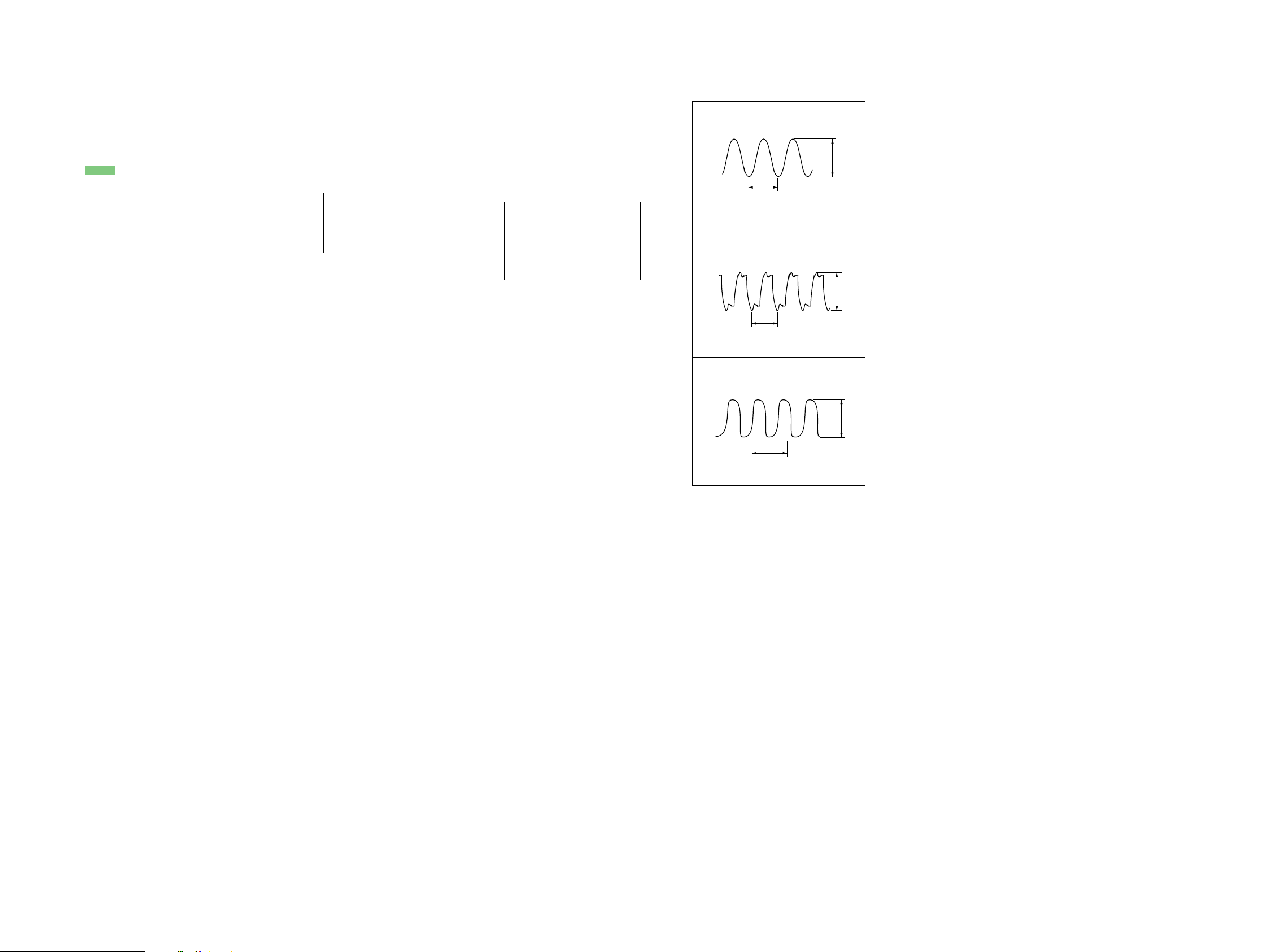
•Waverforms
IC601 ya XO (CD play mode)
1
0.5 V/DIV, 20 ns/DIV
IC801 yd XOUT4M
2
(CD play mode)
1 V/DIV, 50 ns/DIV
IC001 qg X O (RADIO mode)
3
1 V/DIV, 5 µs/DIV
59 ns
1.8 Vp-p
3.5 Vp-p
126 ns
1.6 Vp-p
13.75 µs
D-NF007/NF0070
99

D-NF007/NF0070
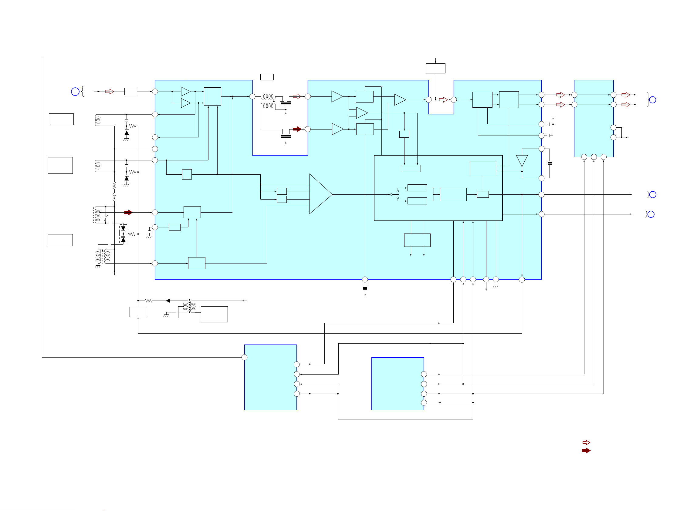
5-1. BLOCK DIAGRAM –CD/POWER SECTION–
IC602 SDRAM(16M)
OPTICAL
PICK-UP
(CDM-3525A)
OP IC
FOCUS
COIL
TRACKING
COIL
(SLED)
(SPINDLE)
VCC
VC
LD
LD-PD
BUSY
BUSY
SEG20
LIQUID
TU L
B
TU R
65
67
COM1
I
51
FIFO
COM4
MUTE
Q101,201
22
LINEOUT_MUTE
IC801(1/2)
67
KEY MATRIX
S802 - S809
SYSTEM
CONTROL
KEY1
KEY2
68
IN1
3
IN2
5
IC802
EEPROM
OPEN/CLOSE
41 40
S811
(OPEN)
OFF ON
SDA
65
245523505349474839
EE_SDA/REM_SDA
HOLD
S812
HOLD
IC1002
INVERTER
TUNER
SECTION
(Page 11)
IC301
HEADPHONE AMP
MUTE
2
SCL7WP
56
EE_SCL
HP_MUTE
CHG_CLK
SYSBUSY
XIN75
59
75kHz
53
TU_CTL
SYSREQ
SYSSEL
X801
8
DDC
IFMUTE
IFBUSY
IFRDY
IFACK
IFRST
BATT+
DC IN
OUT1
OUT2
VCC
60
A
45
54
28
32
26
27
25
30
31
66
65
XOUT75
ANT
1
7
CHG_CLK
SYSBUSY
SYSREQ
SCL
SDA
IFMUTE
IFBUSY
IFRDY
IFACK
SYSSEL
IFRST
CD-VCC
VDD DSP
Q479
TU-VCC
VDD_CORE
Q472
Q471
DC IN DETECT
J301
REMOTE
i
SWITCHING
Q473,474,480
DDC
Q402
VOUT
5
+VBAT
IC603
REG
L403
VIN
TUNER:H
38
30
31
1
C
L402
SWITCHING
Q404
SWITCHING
Q403
IC401 (2/2)
DC/DC CONVERTER
VSYS
DCIN
REGB
D403
+B SWITCH
Q401
TUNER
SECTION
(Page 11)
SW
37
REG0
32
21
PVCC
FB404 F402
FB405
• Signal Path
: CD PLAY
: FM
F401
DRY BATTERY
SIZE "AA"
(IEC DESIGNATION LR6)
2PCS. 3V
J401
DC IN 4.5V
!
DAC
SUBSYQ
SUBSYQ
XIN8M
TUNER
SECTION
(Page 11)
LINE
AMP
MCK
DIN/DOUT
R/W
RW
MCK
DIN OUT
XOUT8M
63
2 - 21 77 - 80
LDACO
RDACO
RESTB
XXRESET
SEG1
I
LCD801
CRYSTAL
DISPLAY
DQ0-15
2,3,5,6,8,9,11,12,39,
40,42,43,45,46,48,49
CD-VCC
REG
Q603
A
B
C
E
F
M
M
CD-VCC
LD
DRIVER
Q601
SLED+
SLED-
SPINDLE+
SPINDLE-
+
T+
SWITCHING
VDD DSP
F+
T-
F-
Q476
BD
3
AC
2
+
E
6
F
7
ASY
10
VBIAS
4
LD
9
PD
8
SWITCHING
CD-VCC
11
18
17
19
20
23
22
25
24
29
80 79
RFI
EQO
RF
SIGNAL
GEN.
APC
Q477
FOCUS/TRACKING COIL DRIVE,
SLED/SPINDLE MOTOR DRIVE
VREF
FO+
DRIVER
FO-
TRK-
DRIVER
TRK+
SLED+
DRIVER
SLED-
SPID+
DRIVER
SPIN-
CT
IC401 (1/2)
AMP
AMP
AMP
AMP
39,42-48
SERVO
SIGNAL
GEN.
DQ00-07
FOCUS
MUTE34
MUTE1
DIGITAL SERVO
SIGNAL PROCESSOR
TRK
SLED
CLV
CLK
RESET
OFF
WP
A0-11
19-24,27-32
PROCESSOR
FDOUT
TDOUT
CLVOUT
13 14 1516
CLV
TRK
FOCUS
FOCUS
10
TRK
9
8
CLV
7
3
4
5
6
2
1
IC1001(2/2)
TUNER CONTROLLER
CHG_CLK
28 27 25 24
32-21
A00-A11
MP3 &
ADPCM CORE
DIGITAL
SIGNAL
SDSOUT
56
SLED
IFMUTE
IFBUSY
RAS
17 16 15
34 35 36 37 38
RASX
CLOCK
XO
CLK88
CLK
X601
16.9344MHz
11
SCL
SDA
IFRDY
23 22 21 18
CAS
WE
LDQM
UDQM
CLK
LDQM
UDQM
16K SRAM
IC471
SHIFT:L
SYSREQ
SYSSEL
CKE
35 34
17 18 19
RCLK
RCKE
7
53
1
RV471
CLOCK
SHIFT
D871
D872
S871
RADIO ON
BAND
CK_CTL2
RESET
WSYSREQ
8
A13
D
FLAG0
SAMPLING
DIGITAL FILTER
DIGITAL SIGNAL PROCESSOR,
SDRAM CONTROLLER,
TUNER
SECTION
(Page 11)
S801
ENTER
30
XIN
2
XOUT
3
XTIN
6
Q602
X8 OVER
IC601
RF AMP, SERVO,
D/A CONVERTER
MUTE2
76
75
MUTE1
57
RESETB
74
P.OFF
44
K_TUNER
43
K_PLAY
INVERTER
Q475
INVERTER
Q475
14 36
WEX
CASX
OSC
XI
6061 535750515254
CLOCK SHIFT
2 6
SWITCHING
Q475
CK_CTL
SYSBUSY
IFACK
17 16 9
7563
AD_MONI0
1 BIT
62
X802
8MHz
D-NF007/NF0070
CHG_CLK
IFMUTE
IFBUSY
SCL
SDA
IFRDY
SYSBUSY
IFACK
SYSREQ
SYSSEL
RESET
1010
5-2. BLOCK DIAGRAM –TUNER SECTION–
D-NF007/NF0070
CD/POWER
SECTION
(Page 10)
L003
FM
TRACKING
L004
FM
FREQUENCY
COVERAGE
CT001, T001
AM
TRACKING
A
(FM OSC)
(AM OSC)
ANT
L003
(FM RF)
L004
L001
AM
FERRITE-BAR
ANTENNA
T001
CT001
TU-VCC
D002
D003
D001
FL001
BPF
LPF
Q002
(VT)
FM/TV RF IN
1
FM RF OUT
30
TV RF OUT
29
28
26
27
AGC
4
25
IC001
FM RF AMP, FM/AM OSC,
FM/AM IF AMP, FM/AM DET, FM MPX, PLL
FM
TV
RF VCC
FM/TV OSC
1/2
AM RF IN
AM OSC
D004
AGC
T003
MIX
AM
AM
OSC
FM/TV
MIX
DC-DC
CONVERTOR
Q003
MIX OUT
3
TU-VCC
T002
AM IF
T002
(AM IFT)
CF001
TU-VCC
CF002
TU-VCC
1/16
1/4
FM/TV1/2
FM1/32
TV1/8
AM
5
7
FM IF IN
AM IF IN
BUFFER
FM IF
AM IF
FM
DET
IF BUFFER
AM
DET
QUAD
8
TU-VCC
CF003
INVERTER
Q001
AF
DET OUT MPX IN
9
1/8
FM
IF IN
FM OSC IN
AM OSC IN
FM/AM/TV
SWITCH
AM
PLL
10
PROGRAM
COUNTER
TU-CE
24
FM MPX MUTE
REFERENCE
DIVIDER
CLK
D-I/O
23
PC
PLL VCC
TU-VCC
PLL GND
172122
INV
DO
20
L OUT
R OUT
LPF1
LPF2
XO
TUNER:H
SHIFT:L
IC901
TU VOLUME
13
14
TU-VCC
11
12
XI
16
X001
15
19
18
L IN
6
R IN
11
MLEN
L OUT
5
R OUT
12
7
AVDD
DVDD
4
MCK
MDT
15 1614
DDC
TU L
TU R
TUNER:H
SHIFT:L
B
C
D
CD/POWER
SECTION
(Page 10)
CD/POWER
SECTION
(Page 10)
CD/POWER
SECTION
(Page 10)
D-NF007/NF0070
FM_H
10
IC1001(1/2)
TUNER
CONTROLLER
PLL_CE
TCK
TDO
12
VOL_EN
TCK
TDO
TDI
37
36
35
34
13
36
TDI
35
IC801(2/2)
SYSTEM
CONTROL
• Signal Path
: FM
: AM
1111

D-NF007/NF0070
5-3. PRINTED WIRING BOARD – MAIN BOARD (SIDE A) –
1
A
2
MAIN BOARD (SIDE A)
B
C
D
R482
R851
R410
R412
Q479
ECB
E
Q475
ECB
RV471
5
IC802
8
C040
R022
R023
R873
R826
R828
R812
R808
R804
R844
R843
4
1
R020
C048
SL801
OPEN
D871
R472
C472
R474
C478
F
G
R477
(EXCEPT AEP)
R476
R473
C473
C474
R475
1
IC471
4
C471
8
5
R411
C805
D004
R021
C049
Q003
BCE
C047
R026
L006
H
3 4 5 6 7
Q477
L406
R1011
R1012
R1003
R1010
R1016
(AEP)
R824
R1015
R1014
R821
R872
15
16
IC1001
R871
R848
R846
R847
R849
C882
C880
R845
SL803
R484
C480
R817
R810
C814
R874
RB806
1
R1019
C812
C806
C407
L407
R1017
30
L450
BCE
C877
VDR802
C802
C807
R305
C303
SL871
C874
ECB
Q804
C405
R404
R1018
R876
R419
R614
C611
C604
C450
C403
:Uses unleaded solder.
FB301
IC301
R418
1
4
R1013
C475
RB305
1
20
R823
R417
Q476
ECB
Q402
C108 C208
C205
C202 C102
C618
80
21
R850
C815
C808
C811
R416
Q401
R829
R480
R403
C105
C809
D403
8
5
RB302
R104
RB304
IC601
Q803
BCE
R877
R481
RB303
D401
RED
C876
R307
C101
R308
61
40
C875
BLK
C201
RB620
R408
R483
C625
60
C619
R629
41
FB603
C637
R835
C402
ORG
GRY
1-868-220-
R624
Q602
R619
ECB
C901 C902
C908
R811
C903
C909
12
(12)
CT001
TAP005
RF GND(A)
L003
R301
OPTICAL PICK-UP
R005
R009
C027
C044
R036
C042
C041
(CDM-3525A)
(1/2)
+
(SLED)
M
–
–
(SPINDLE)
M
+
C008
C010
TAP001
RF(B)
L008
R006
CF001
CF002
R401
R402
C401
D420
8
9
• Semiconductor
Location
Ref. No.
D004 F-2
D401 G-4
D403 G-4
D404 E-8
D420 E-8
D871 E-1
IC301 B-4
IC471 F-2
IC601 D-4
IC802 F-2
IC1001 E-3
Q003 F-2
Q401 G-4
Q402 G-4
Q475 E-2
Q476 G-4
Q477 E-3
Q479 D-2
Q602 C-5
Q803 F-4
Q804 F-4
C470
FB404
D404
VDR418
F402
FB403
Location
D-NF007/NF0070
1212

D-NF007/NF0070
Ver. 1.1
5-4. PRINTED WIRING BOARD – MAIN BOARD (SIDE B) –
1
2
A
3 4 5 6 7
MAIN BOARD (SIDE B)
B
T001
C
T002
C013
C017
L002
D
R027
C050
CF003
C028
F401
E
DRY BATTERY
SIZE "AA"
(IEC DESIGNATION LR6)
J401
DC IN 4.5V
2PCS. 3V
F
G
H
C033
C036
R008
C009
C034
C029
R017
Q001
ECB
R030
C016
1
C025C026C030
IC001
15
C038
C039
D402
OPTICAL PICK-UP
(CDM-3525A)
(2/2)
FL001
TAP003
RF GND(B)
30
16
C043C045
X001
:Uses unleaded solder.
L001
AM
FERRITE-BAR
ANTENNA
NATURAL
GREEN
D002
C011
C018
S
G
C046
R018
C021
R109
D
R004
C024
C006
L004
C031
C032
TP006
R015
TP406
M-GND
D003
VT
R024
D001
C019
TP013
GND
R012
RED
C003
C012
R014
R011
R002
R016
C035
C002
R001
C005
TP012
TUL
8
9
RB901
C023
TAP001
C014
TP002
Q002
C022
RF(A)
C020
R007
C037
L005
R013
TP014
TUR
R902
R901
IC901
R906
R1008
C476
C910
R1009
Q474
Q403
ECB
1
16
FB901
R905
C905
C906
R902
C907
8
9
• Semiconductor
S811
(OPEN)
TP802
OPEN
C004
Q102
R103
C109
C631
R626
R621
C626
SPINDLE+
20
21
FB401
TP416
R203
R672
C810
C209
R303
R204
X801
C612
C633
CB414
C412
C410
C411
R881
R882
C813
C301
TP604
R606
C606
FB606
C632
R1004
R820
C827
IC401
C404
Q101
X601
R618 R622
R904
1
FB601
C638
C624
C620
C629
50
IC602
R617
R478
ECB
Q472
R485
R414
Q480
ECB
R415
L007
ECB
TP416
SLED-
L403
C419
C408
26
TP416
SLED+
C420
C477
C421C417
C406
TP416
SPINDLE-
C627
FB604
FB605
S803
.
TUNE
FB402
25
Q471
BCE
R471
Q473
ECB
L402
C481
TP471
SIFT
C416
BCE
Q404
S802
>
TUNE
(AEP,3AEP,EE)
FB101
C106
R102
FB201
RF
C634
C605
R632
IC603
5
1
R630
C615
C609
R620
R615
R613
4
3
R605
R604
R603
IC1002
40
41
60
61 80
R879
C881
R875
X802
1
40
R407
C452
C453
D872
R856
S801
u
ENTER
R202C206
R304
D201
R608
R601
16
15
Q601
5
C1001
IC801
R409
C413
R406
C409
D101
R111
C104
C110
1
ECB
C603
R405
S807
RADIO OFF
2
x
R101
R607
CN501
C601
C607
34
1
R1001
R211
C204
C210
R201
C602
Q603
C610
C454
C623
R1005
21
T003
1-868-220-
RB301
R674
C628
20
1
S808
SOUND/AVLS
C305
R602
R675
BCE
R673
C640
J301
REMOTE
i
C304
FB305
S812
HOLD
OFF ON
24
S806
GROUP
.
T
P MODE/
CN801
12
(12)
S809
R852
R853
R854
S804
VOL+
R880
S805
VOL–
S871
RADIO ON
BAND
1
LCD801
LIQUID CRYSTAL
DISPLAY
Location
Ref. No.
D001 C-4
D002 C-4
D003 D-4
D101 B-7
D201 B-7
D402 E-3
D872 H-6
IC001 C-3
IC401 G-6
IC602 D-5
IC603 D-6
IC801 F-7
IC901 C-5
IC1002 E-7
Q001 D-3
Q002 D-4
Q101 B-6
Q102 B-6
Q403 F-5
Q404 G-5
Q471 F-5
Q472 F-5
Q473 F-5
Q474 F-5
Q480 F-5
Q601 D-7
Q603 D-7
Location
D-NF007/NF0070
1313

D-NF007/NF0070
5-5. SCHEMATIC DIAGRAM – MAIN BOARD (1/3) –
*
2.2k
R005
C011
470k
0.01
L003
FM
C006
5p
C008
220p
C010
150p
TP001
RF(B)
C022
5p
FM
RF GND(B)
TRACKING
/TV RF AM
/TV/AM
FM
TP003
C012
0.01
AM
TB2132FNG
IF AM
FM
FL001
L001
AM
FERRITE-BAR
ANTENNA
CT001
10p
C002
2200p
C003
0.022
R001
470k
R002
1k
CT001,T001
AM
TRACKING
D001
C005
0.1
TP002
RF(A)
D002
HVC202B TRU
R004
470k
C024
220p
1 R007
NF007: EXCEPT CND
1k
NF007: CND/NF0070
L003
FM
T001
OSC
C014
0.022
IC001
P,FM/TV/AM
P,FM
PX,PLL
M
RF GND(A)
• See page 9 for Waveforms. • See page 9 for IC Block Diagrams.
TP006
RF
C020
0.01
/AM
TP005
OSC,
DET,
C050
0.01
R031
R006
L008
R007
*
0
22
0H
1
C023
4.7
C018
5p
FM
L004
FM
FREQUENCY
COVERAGE
C016
1000p
L004
OSC
FM-RF O
FM/TV I
C021
150p
C019
0.01
HVC202B TRU
TV-RF O
GND
C026
0.1
D003
RF-VCC
MIX O
R009
10k
1000p
C027
AM-RF
AGC
C025
4.7
C028
0.1
C044
1000p
FM/TV-OSC
FM-IF I
R011
220
AM-OSC
VCC
VT
TU CE
C032
0.22
S
R012
220
TU-CE
AM-IF I
Q002
2SK3019TL
LPF
TCK
CLK
QUAD
10.7MHz
C029
470p
CF003
C009
0.01
D I/O
DET-O
C030
0.1
R014
15k
VDD
MPX IN
R017
3.3k
C033
0.1
C031
0.01
R019
10k
DO
LPF1
C034
R016
47k
C035
1
2.2
R020
TUNER:H
LPF2
C036
0.1
R030
0
10k
C037
SIFT:L
L O
C038
1
0.01
D004
1SS355TE-17
C040
0.01
L005
0H
X I
D-GND
R O
X O
C039
0.01
R021
C041
0.1
C042
1k
0.1
C046
C043
15p
X001
75kHz
C045
22p
R036
C047
5p
Q003
2SC4154-F
0
R013
L006
0H
R024
TP012
TP014
47k
R901
10
R902
10
TUL
TUR
DC/DC CONVERTER
R023
C049
220
0.01
C901
4.7
C902
C903
4.7
4.7
RB901
0
C909
2200p
R015
220
VRL
VRR
AVDD
AVSS
C908
0
R022
100k
C048
C906
LIN
RIN
C907
4.7
ADRS1
MCK
FB901
0
C905
RSTN
MDT
1
IC901
6451BV-E2
SM
TU VOLUM
R904
220
R905
220
R906
220
E
TCK
VOL EN
1
LOUT
DVDD
ADRS2
ROUT
DVSS
MLEN
C910
1000p
1
T003
DC-DC CON
4.7
0
220
R018
R026
0
D-NF007/NF0070
TAP001
ANT
R027
22
L002
C013
47
6.3V
0H
Z002
C017
0.1
CF001
10.7M
R008
470
Hz
T002
AM
T002
AM
IFT
CF002
450KHz
IF
AIN
M
BOARD
(2/3)
(Page 15)
Q001
RT1P140M
INVERTER
-TP-1
FM/AM
SIFT:L
GND
RB902
4.7k
TU R
TU L
L007
BUS 2
R1009
R1008
0
DDC
TU VCC
TU GND
TUNER:H
AIN
M
BOARD
(3/3)
(Page 16)
1k
1k
TDI
TDO
1414

D-NF007/NF0070
5-6. SCHEMATIC DIAGRAM – MAIN BOARD (2/3) –
R602
220
603
Q
A2018TL
2S
REG
UDZSTE-176.2B
R403
1k
Q401
2SB1132-T100-Q
+B SW
D403
RB160M
D401
ITCH
-30TR
CN501
16P
Q402
H8N-TR
UM
DC IN DETECT
R675
2.2
C
E
A
B
F
VCC
VC
GND
D
GN
LD-PD
LD
L406
NC
L407
47uH
47uH
F+
T+
TF-
FB402
0H
CN403
404
CN
FB401
0
408
CN
CN407
C404
10
C403
16V
0.1
C408
100
6.3V
C409
C450
10
16V
1
R405
12k
C452
1
19
C475
220p
673
C640
R
4.7
100k
R674
4.7k
C602
47
6.3V
C407
10
1
C412
0.1
C410
220p
C411
L450
1000uH
R407
R406
27k
10k
Q476
RTN144M
ITCHING
SW
C406
0.1
C453
470p
C413
0.022
-TP-1
M
C454
10
C603
0.01
R603
4.7
2SA1602TP-1EF
LD
FOCUS/TRACKING COIL DRIVE,
SLED/SPINDLE M
608
R
R607
C601
R604
47
100k
6.3V
R
Q601
IVER
DR
IC401
BH6575FV-E2
OTOR DRIVE,
DC/DC CONVERTER
PVCC
SLED+
SLEDSPINDSPIND+
DPG2
SPRT
SOFT
CT
DCIN
REGB
FOCUS
REGO
PRGND
PGND
LG
VG
M
SW
M
VSYS
EI
EO
605
0
TRK+
DPG1
VREF
SLED
RESET
UTE1
UTE34
10k
10k
C606
0.1
TRK-
FO+
FO-
FIL4
FIL3
FIL2
FIL1
TRK
CLV
CLK
OFF
P
W
• See page 9 for Waveforms. • See page 18, 19 for IC Block Diagrams.
SIFT:L
/AM
RB303
R307
470
0
C101
308
R
2200p
0
FB601
LDACO
EX
W
E
LDQM
W
R1012
1M
XOUT
(CHG CLK)
31
AGND2
LDQM
UDQM
0
XIN
SEL
AM
32
FLAG0
DVDD2
DQ07
UDQM
DQ07
R1013
GND
CK CTL2
VD
R1017
R1019
RB620
D
22k
0
10k
XO
DG
R
SUBSYQ
IN/DOU
D COR
DVDD1
DGND1
0
33
0
ESETB
CLK88
BUSY
DQ00
DQ01
DQ02
DQ03
DQ04
DQ05
DQ06
C625
2.2
R
XI
ND2
TEST
CLK
CK
M
T
R/W
E2
35
C620
0.1
C628
10
626
R
220
C618
470p
RFI
ONI1
ANA M
A10
A09
A10
A09
A08
TDI
0
0
22
16V
I0
VDD RD
HPRDAC0
AD MONI1
AD MON
ANA MONI0
P,SERVO,DIGITAL SIGNAL
RF AM
CONTROLLER ,D/A CONVERTER
SD RAM
A08
A07
A06
A05
A04
A07
A05
A06
A04
TDO
TCK
0
TU CE
R1010
TDI
TCK
TDO
PLL CE
CK CTL1
SYSSEL
SYSREQ
IFACK
NC
NC
R1014
0
23
24
VSS LD
VSS RD
IC601
BU9541AKV
A03
A02
A03
A02
H
FM
SYSREQ
W
SYSBUSY
IFRDY
25
26
C631
0.1
HPLDACO
A01
A01
RESET
SDA
27
VDD LD
A00
A00
XTOUT
SCL
28
AVDD2
VDD CORE1
RAS
XTIN
SY
IFBU
29
DACO
R
ASX
R
VCPU
C
N
C1001
VCDAC
CASX
CAS
10
SL1001
TEST
IFMUTE
30
PROCESSOR,
R1018
C629
2.2
620
R
R601
10k
10k
R615
68k
R623
RT1N140M
SW
Q475
ITCHING
-TP-1
0
R850
0
R617
100
CLK
CKE
R1001
0H
C605
0.1
C607
47
6.3V
C615
2200p
C609
613
R
2200p
68k
R606
220k
C604
0.1
CB414
0.022
R480
100k
22k
R416
100k
R417
47k
R418
22k
R419
R481
100k
R409
0
15
14
13
16
11
3
Q477
-TP-1
RT1P140M
HING
ITC
SW
4.7
50V
H240FK
RV471
R476
C473
C474
470
R614
10k
15k
R477
470k
10p
8p
C610
0.22
C611
CLOCK
SHIFT
IC471
TC7W
Y1
A2
G2
VCC
CLOCK SHIFT
G1
A1
Y2
GND
R411
470k
R473
C471
0.1
R482
2.2k
R475
100k
C472
10k
100p
R474
0
C478
470p
R472
4.7k
C612
0.1
P86C808DM
TM
CONTR
TP604
AVDD
AC
BD
VBIAS
AGND
E
F
PD
LD
ASY
PCO
FCO
FDOUT
TDOUT
SDOUT
CLVOUT
RCLK
RCKE
A13
A12
R1011
IC1001
-6F65
TUNER
R621
R
OLLER
0
F
EQO
1
1
A11
A11
0
R1015
R1016
G
RB304
470
C201
2200p
C638
1
T1N140M
R
BU
618
1M
R1003
C102
C202
C105
1000p
1000p
626
C
0.01
C624
0.1
602
Q
FFER
R622
220
619
C
0.1
DQ
DQ01
DQ02
DQ03
DQ04
DQ05
DQ06
0
R1005
34
-TP-1
16.9344M
R
100k
R629
00
22k
R619
100k
X601
z
H
R811
100k
624
2
8
4
0
6
7
5
FB603
0
C637
0.1
C205
2.2
2.2
B302
R
4.7k
Q102
-TR
D2N
M
U
ITCH
UTE SW
M
C108
470p
C208
470p
RB305
220k
IC301
BH3544F-FE2
HEADPHO
FB305
9
C632
0.1
IC1002
BU4S584G2
INVERTER
Y
VDD
FB606
VSS
A
NC
C633
0.1
D
GN
P
NE AM
2
IN
0H
C301
0.1
IC603
BH15FB1W
0H
REG
T
VOU
VIN
VSS
C634
R630
1
0
C303
1
IN1
OUT1
MUTE
BIAS
VCC
OUT2
R303
1M
C304
100
C305
6.3V
47
6.3V
G
FB604
0H
NC
CE
FB605
0H
20
DQ00
DQ01
DQ02
DQ03
DQ04
DQ05
DQ06
DQ07
LDQM
W
CAS
RAS
A11
A10
A00
A01
A02
A03
1000p
1000p
E
C109
C209
0.068
0.068
R103
R203
220
220
R104
R204
1M
AEP,3AEP,EE
.8STE61
D101
RSB6
DQ00
DQ01
DQ02
DQ03
DQ04
DQ05
DQ06
DQ07
UDQM
1M
C004
220p
C106
0.22
102
R
2.2
C206
0.22
202
R
2.2
AEP,3AEP,EE
D201
RSB6.8STE61
CLK
CKE
A09
A08
A07
A06
A05
A04
101
Q
H8N
UM
UTE
M
C104
220
6.3V
C204
220
6.3V
C110
C210
R101
10
R201
R305
220k
FB301
10
RB301
0H
1k
VCC
DQ0
DQ1
VSSQ
DQ2
DQ3
VCCQ
DQ4
DQ5
VSSQ
DQ6
DQ7
VCCQ
LDQM
W
CAS
RAS
CS
A11
A10
A0
A1
A2
A3
VCC
R
R211
304
R
IC602
12L16161A-7T(G)
M
SDRAM
16M
E
FB101
111
10
0H
FB201
10
0H
0
VSS
DQ15
DQ14
VSSQ
DQ13
DQ12
VCCQ
DQ11
DQ10
VSSQ
DQ9
DQ8
VCCQ
NC
UDQM
CLK
CKE
NC
A9
A8
A7
A6
A5
A4
VSS
C627
4.7
R672
0
FM
AIN
M
ARD
BO
(1/3)
TU L
TU R
ANT
BU
(Page 14)
S 2
J301
TE
O
REM
D-NF007/NF0070
B+
+VBAT
GND
BUS
CD VCC
AIN
M
BOARD
(3/3)
(Page 16)
DDC
VDD DSP
D GND
BUS 2
1515

D-NF007/NF0070
5-7. SCHEMATIC DIAGRAM – MAIN BOARD (3/3) –
S801
L403
10uH
C420
220
6.3V
C477
1
D402
RB160M-30TR
S802
DDC
S803
S808
S807
FB404
4.7uH
VDR418
FB403
4.7uH
R835
0H
R847
2.2k
R845
10k
R849
2.2k
R856
4.7k
R851
22k
1
14
19
C480
0.022
R484
47k
C807
1
R810
1M
C405
1000p
R404
100
L402
165uH
C476
1
DRY BATTERY
SIZE"AA"
(IEC DESIGNATION R6)
2PCS.3V
J401
DC IN 4.5V
D871
MC2838
TP471
CN401
SIFT
C481
47p
Q403
2SD2652T106
SWITCHING
TP406
M GND
CN402
C416
S871
47p
R880
470
Q404
2SD2652T106
SWITCHING
C417
0.1
UDZS-TE17-12B
UDZS-TE17-12B
MC2838
R415
1k
R414
10
C421
1
F401
32V
D420
D404
D872
2A
B+
R881
470
F402
1.4A
32V
C419
220
6.3V
+VBAT
• See page 9 for Waveforms. • See page 20 for IC Pin Function Description.
MAIN
BOARD
(2/3)
(Page 15)
BUS
R817
10k
RB806
47k
C874
0.01
R846
10k
2SC4081T106
INVERTER
C875
1000p
Q804
2SC4081T106
INVERTER
R876
R848
2.2k
S804
S805
S809
S806
47k
Q803
C814
470p
R485
R877
47k
R852
2.2k
R853
4.7k
R854
32
C812
C802
0.01
470p
C806
0.1
22k
C401
1
0
CD VCC
GND
RT1P140M-TP-1
C470
2200p
VDD DSP
13
Q471
+B SWITCH
R1004
0
C872
12p
R882
0
GND
XIN8M
XOUT8M
VDD
DC IN
BATT+
KEY1
KEY2
TEST
WREM
SEL OPTION
NC
TEST1
P.OFF
MMUTE1
MMUTE2
COM1
COM2
COM3
COM4
Q473
RT1N140M-TP-1
SWITCHING
34
R829
100k
R823
XOUT75
SEG0
C811
0.1
1k
XIN75
SEG1
SEG01
VDR802
C876
22p
X802
8MHz
R821
100k
R874
C880
SL803
SL802
33
C881
1000p
R875
1k
100k
470p
TEST
R871
ICE
COM1
COM2
COM3
COM4
*1 R871
100k
220k
*2 R872
47k
220k
RT1N144M-TP-1
SWITCHING
R879
1M
R872
*1
C882
AEP,3AEP,EE
E19,8E19,AUS
NF007: EXCEPT CND
NF007: CND/NF0070
R471
100k
Q474
X801
75kHz
*2
1000p
R410
0.22
C813
10p
R820
2.2M
2SA2018TL
+B SWITCH
R478
4.7k
Q472
15
16
C877
22p
C808
1
R408
0H
C402
1000p
R402
22k
R401
100k
TEST0
SEG2
SEG02
11
RESETB
SEG3
SEG03
20
HP MUTE
SEG5
SEG4
SEG05
SEG04
R412
4.7k
30
TU CTL
SEG06
3
4
2
VDD
FIFO
BUSY
RESET
IFMUTE
IC801
BU18704-S5
SYSTEM CONTROL
SEG10
SEG9
SEG7
SEG8
SEG6
SEG09
SEG10
SEG07
SEG08
5
6
RW
MCK
SEG12
SEG11
SEG11
SEG12
Q479
2SA2018TL
+B SWITCH
7
31
NC
DIN OUT
(CHG CLK)
TCK(IFCON&VOL CLK)
TDO(IFCON&VOL DATA)
SEG16
SEG15
SEG14
SEG13
SEG15
SEG16
SEG13
SEG14
Q480
RT1N140M-TP-1
SWITCHING
R483
10
R824
2.2k
R873
2.2k
SL871
TU TEST
K PLAY
TU TEST
K TUNER
TDI(IFCON)
SYSBUSY
EE SDA/REM SDA
LINEOUT MUTE
SEG17
SEG19
SEG18
SEG19
SEG17
SEG18
C809
0.1
R812
100k
R826
0
OPEN/CLOSE
HOLD
SUBSYQ
LINE DET
VOL EN
GND
IFRDY
IFRST
SYSSEL
SEL CEX
IFBUSY
IFACK
SYSREQ
EE SCL
SEG20
C623
470
6.3V
C810
SEG11
VOL EN
SEG12
TCK
TDO
SEG13
TDI
SEG14
SDA
SCL
WP
VCC
BUS 2
IC802
BR24L02F-WE2
EEPROM
GND
SEG16
SEG15
SEG17
5
A2
A1
A0
SEG18
26
35
22
29
24
25
23
28
27
9
SEG19
SEG20
1
CN801
24P
D GND
8
10
SEG20
AEP
R808
100k
COM1
24
COM2
EXCEPT AEP
R843
10k
R844
10k
COM4
COM3
R828
2.2k
C815
0.1
SEG01
20
R804
SEG02
0
SEG03
SEG04
SEG05
SL801
SEG06
15
OPEN
OFF
ON
SEG08
SEG07
LIQUID
CRYSTAL
DISPLAY
HOLD
C805
0.1
SEG09
S811
(OPEN)
S812
SEG10
10
D-NF007/NF0070
DDC
TU VCC
TU GND
MAIN
BOARD
(1/3)
(Page 14)
TUNER:H
1616

• IC Block Diagrams
IC001 TB2132FNG
D-NF007/NF0070
TV
RF
FM
RF
1
FM/TV RF IN
FM RFOUT
29
30
TV RFOUT
28
2
GND
RF VCC
27
AM
MIX
FM/TV
AM RFIN
26
OSC
1/2
MIX
3
MIX OUT
FM/TV OSC
AM OSC
25
AM
OSC
TV 1/8
1/16
AGC
4
AGC
AM
1/4
FM 1/32
FM/TV 1/2
BUFFER
IF
BUFFER
FM
IF
IFIN
AM FM
5
FM IFIN
1/8
AM
IF
6
VCC
AM OSCIN
FM OSCIN
DET
DET
7
AM IFIN
FM
AM
8
QUAD
PLL
AF
9
DET OUT
CE
23CK24
PROGRAM
COUNTER
FM/AM/TV
SWITCH
10
PLL VCC18OUT1 (ST)
DATA
21
22
COMPARATOR
FM MPX
12
LPF111LPF2
MPX IN
OUT2 (DO2)
DO
19
20
PHASE
REFERENCE
DIVIDER
MUTE
13
14
L-CH
R-CH
PLL GND
17
XI
16
15
XO
IC901 SM6451BT-G-E2
RSTN
ADRS1
ADRS2
DVDD
LOUT
LIN
AVDD
VRL
16
1
INTERFACE
CONTROL
2
3
4
5
6
7
8
CHIP
ADDRESS
DECODER
1/2VDD
ATTENUATION
CONTROL
ATTENUATION
CONTROL
REFERENCE
VOLTAGE
CIRCUITS
ATTENUATION
DECODER
1/2VDD
MDT
15
MCK
14
MLEN
13
DVSS
12
ROUT
11
RIN
10
AVSS
9
VRR
17

D-NF007/NF0070
+
67 58
+
2
1 3 4
OUT 1
XMUTE
MUTE
IN 1
GND
VCC
OUT 2
BIAS
IN 2
BIAS
TSD
24.7k
24.7k
16.9dB
16.9dB
IC401 BH6575FV-E2
EO
40
SYSTEM
ON
1
WP
–
+
SYSTEM
OFF
2
OFF
SPIND–
15
FIL4
SPIND+
24
25
26
PRE-DR
–
+
–
+
–
+
–
+
PRE-DR PRE-DR
16
DPG1
17
FO–
29
11
VREF
12
FIL1
SOFT
28
14
FIL213FIL3
REG
VSYS
+
30k
31
–
10
FOCUS
DCIN30CT
+
35
6
VG
CONV
30k
PGND
33
34
DETECT
30k
–
8
SLED
–
+
9
TRK
–
+
30k
7
CLV
DC/DC
4
MUTE34
37
MUTE1
MUTE1
VG36LG
RESET
5
RESET
VSYS38SW
EI
39
VSYS
–
–
CONVERTER
+
OSC
CLK
MUTE34
3
CLK
REGO32REGB
PRGND
SPRT27DPG2
18
FO+
SLED+
23
PRE-DR
SLED–
22
19
TRK–
PVCC
21
20
TRK+
IC471 TC7WH240FK
GND
18
IC301 BH3544F-FE2
G1
1
A1
2
Y2
3
4
8
VCC
7
G2
Y1
6
5
A2

IC601 BU9541AKV
ANA_MONI1
EQO
RFI
ANA_MONI0
AD_MONI1
AD_MONI0
80 79 78 77 76 75 74 73 72 71 70 69
VDD_RD
HPRDACO
VSS_RD
VSS_LD
HPLDACO
VDD_LD
AVDD2
RDACO
VCDAC
LDACO
AGND2
68 67 66 65 64 63 62 61
FLAG0
D-NF007/NF0070
DVDD2
XO
AVDD1
VBIAS
AGND1
ASY
PCO
FCO
FDOUT
TDOUT
SDOUT
CLVOUT
RCLK
RCKE
A13
A12
1
2
AC
BD
3
4
5
6
E
7
F
8
PD
LD
9
10
11
12
13
14
15
16
17
18
19
20
RF
SIGNAL
GENERATOR
APC
PLL
DIGITAL
SERVO
SIGNAL
PROCESSOR
SERVE
SIGNAL
GENERATOR
D CLASS HP
AMPLIFIER
DIGITAL
SIGNAL
PROCESSOR
16K SRAM
MP3
&
ADPCM
CORE
LINE
AMPLIFIER
1 BIT DAC
X8 OVER
SAMPLING
DIGITAL FILTER
60
59
58
57
56
55
54
53
52
51
50
49
48
47
46
45
44
43
42
DQ06
41
XI
DGND2
TEST
RESETB
CLK88
CLK
SUBSYQ
BUSY
MCK
DIN/DOUT
R/W
VDD_CORE2
DQ00
DQ01
DQ02
DQ03
DQ04
DQ05
DVDD1
21 22 23 24 25 26 27 28
A11
A10
A09
A08
A07
A06
A05
30 31 32 33 34
29
A04
A03
A02
A01
A00
35
RASX
VDD_CORE1
36 37 38 39 40
WEX
CASX
LDQM
UDQM
DQ07
DGND
19

D-NF007/NF0070
5-8. IC PIN FUNCTION DESCRIPTION
• IC801 BU18704-S5 (SYSTEM CONTROLLER)
Pin No. Pin name I/O Description
1 SEG0 O Not used (OPEN)
2 to 21 SEG1 to SEG20 O LCD segment output
22 LINEOUT_MUTE O Mute signal output
23 EE_SDA/REM_SDA I/O EEPROM data
24 EE_SCL O EEPROM clock
25 SYSREQ O Request output to IC1001
26 SYSBUSY O BUSY output to IC1001
27 IFACK I ACK input from IC1001
28 IFBUSY I BUS BUSY input from IC1001
29 CEL_CEX I Select model
30 SYSSEL O Master/Slave select signal output to IC1001
31 IFRST O Reset output to IC1001
32 IFRDY I IFRDY input from IC1001
33 GND – Ground terminal
34 TDI (IFCON) I Data for serial communications input
35
TDO (IFCON&VOL DATA)
36 TCK (IFCON&VOL CLK) O Clock for serial communications output
37 VOL_EN O Volume enable output to IC901
38 LINE_DET I Not used (OPEN)
39 SUBSYQ I Sub code sync interruption input
40 HOLD I HOLD switch status detection input
41 OPEN/CLOSE I OPEN switch status detection input
42 TU_TEST I Tuner test terminal
43 K_PLAY I PLAY KEY input
44 K_TUNER I TUNER KEY input
45 (CHG_CLK) O Clock select phase match output
46 NC O Not used (OPEN)
47 DIN OUT I/O Command output , DSP status input, subcode Q input
48 MCK O Serial interface clock output
49 RW O DSP’s serial interface Read/Write signal output
50 BUSY I DSP’s auto sequencer status
51 FIFO O SDRAM initialize output
52 VDD – Power supply for CPU and I/O
53 XRESET O System reset output
54 IFMUTE I Phase match with IC1001
55 TU_CTL O Tuner power control output
56 HP_MUTE O Headphone IC mute ON/OFF control output
57 RESETB I Microcomputer reset terminal
58 TEST0 I Connect to GND
59 XIN75 I 75kHz clock input
60 XOUT75 O 75kHz clock output
61 GND – Ground terminal
62 XIN8M I 8MHz clock input
63 XOUT8M O 8MHz clock output (OPEN)
64 VDD – Power supply for CPU and I/O
65 DC_IN I DC IN voltage monitoring input
O Data for serial communications output
20

Pin No. Pin name I/O Description
66 BATT+ I Batt+ terminal voltage monitoring input
67 KEY1 I Key matrix detect input
68 KEY2 I Key matrix detect input
69 TEST I Test mode terminal
70 WREM I Wired remotecontroler key detection input
71 SEL_VERSION I Select version
72 NC I Connect to GND
73 TEST1 I Test mode terminal (not used)
74 P.OFF O Power OFF control output
75 MMUTE1 O Spindle motor drive mute output
76 MMUTE2 O Focus/Tracking drive mute output
77 to 80 COM1 to COM4 O LCD common output
D-NF007/NF0070
21

D-NF007/NF0070
• IC1001 TMP86C808DMG-6F65 (TUNER CONTROLLER)
Pin No. Pin name I/O Description
1 GND – Ground terminal
2 XIN I 8MHz clock input
3 XOUT O 8MHz clock output
4 TEST I Fixed at ground
5 VCPU – Power supply terminal
6XTIN I 75kHz clock input
7XTOUT O 75kHz clock output
8 RESET I Reset input from IC801
9WSYSREQ I Request input from IC801
10 FM_H O AM/FM select signal output to PLL IC(IC001)
11 CK_CTL1 O CLOCK IC(IC471) control output
12 PLL_CE O Chip enable output to PLL IC(IC001)
13 TCK I Clock for serial communications input from IC801
14 TDO I Data for serial communications input from IC801
15 TDI O Data for serial communications input to IC801
16 SYSSEL I Master/Slave select signal input from IC801
17 SYSREQ I Request input from IC801
18 IFACK O ACK output to IC801
19 NC I/O Not used
20 NC O Not used
21 SYSBUSY I BUSY input from IC801
22 IFRDY O IFRDY signal output to IC801
23 SDA O Serial communications data output to EEPROM(IC802)
24 SCL O Serial communications clock output to EEPROM(IC802)
25 IFBUSY O BUS BUSY signal output to IC801
26 NC I/O Not used
27 IFMUTE O Phase match with IC801
28 (CHG_CLK) I Clock select phase match
29 AM_SEL I AM clock shift select signal input(fixed at ground in this set)
30 CK_CTL2 O Clock shift circuit control output
22

SECTION 6
EXPLODED VIEWS
D-NF007/NF0070
NOTE:
• -XX and -X mean standardized parts, so they
may have some difference from the original
one.
• Items marked “*” are not stocked since they
are seldom required for routine service.
Some delay should be anticipated when
ordering these items.
• The mechanical parts with no reference
number in the exploded views are not supplied.
• Color Indication of Appearance Parts Example:
KNOB, BALANCE (WHITE) . . . (RED)
R R
Parts of Color Cabinet’s Color
9
8
•Accessories are given in the last of the
electrical parts list.
• Abbreviation
3AEP : UK model
8E19 : Philippines model
AUS : Australian model
CND : Canadian model
E19 : Singapore model
EE : East European model
10
11
9
17
19
7
16
The components identified by mark 0
or dotted line with mark 0 are critical
for safety.
Replace only with part number specified.
Les composants identifiés par une
marque 0 sont critiques pour la sécurité.
Ne les remplacer que par une pièce
portant le numéro spécifié.
12
13
14
6
15
4
5
18
3
20
1
2
Ref. No. Part No. Description Remark Ref. No. Part No. Description Remark
1 2-638-196-01 BUTTON (B) (SILVER)
1 2-638-196-11 BUTTON (B) (WHITE)
1 2-638-196-21 BUTTON (B) (BLACK)
2 2-638-197-01 KNOB (HOLD) (SILVER)
2 2-638-197-11 KNOB (HOLD) (WHITE)
2 2-638-197-21 KNOB (HOLD) (BLACK)
3 2-596-449-01 TERMINAL (RELAY), BATTERY
4 2-638-934-01 BUTTON (A) (SILVER)
4 2-638-934-11 BUTTON (A) (BLACK)
4 2-638-934-31 BUTTON (A) (WHITE)
9 3-245-331-02 INSULATOR
010 A-1112-193-A OPTICAL PICK-UP CDM-3525A
11 X-2067-449-1 LID ASSY (B) (A), UPPER (BLACK) (NF007)
11 X-2067-451-1 LID ASSY (S), UPPER (SILVER) (NF007)
11 X-2067-452-1 LID ASSY (B) (L), UPPER (BLACK) (NF0070)
11 X-2067-802-1 LID ASSY (S) (L), UPPER (SILVER) (NF0070)
11 X-2102-352-1 LID ASSY (W), UPPER (WHITE) (NF007)
12 2-596-453-03 SPRING (UPPER LID)
13 2-660-036-01 CABINET (MIDDLE) (CND)
13 2-660-036-11 CABINET (MIDDLE) (EXCEPT CND)
5 X-2103-447-1 CABINET (LOWER) (B) SUB ASSY (BLACK)
5 X-2103-449-1 CABINET (LOWER) (S) SUB ASSY (SILVER)
5 X-2103-450-1 CABINET (LOWER) (W) SUB ASSY (WHITE)
6 2-596-447-01 TERMINAL (+), BATTERY
7 2-596-448-01 TERMINAL (–), BATTERY
8 A-1143-674-A MAIN BOARD, COMPLETE (NF007: CND/NF0070)
8 A-1143-677-A MAIN BOARD, COMPLETE (NF007: AEP)
8 A-1143-680-A MAIN BOARD, COMPLETE (NF007: 3AEP, EE)
8 A-1143-683-A MAIN BOARD, COMPLETE (NF007: AUS)
8 A-1143-686-A MAIN BOARD, COMPLETE (NF007: E19, 8E19)
14 2-596-454-03 LID, BATTERY CASE (WHITE)
14 2-596-454-13 LID, BATTERY CASE (SILVER, BLACK)
15 2-596-441-01 SPRING (OPEN)
16 2-638-194-01 KNOB (OPEN) (SILVER)
16 2-638-194-11 KNOB (OPEN) (WHITE)
16 2-638-194-21 KNOB (OPEN) (BLACK)
17 3-254-070-01 SCREW
18 2-659-212-01 CASE, SHIELD
19 2-661-945-01 SHEET (COIL)
20 2-662-461-01 SHEET (BATT)
23

D-NF007/NF0070
Ver. 1.1
MAIN
SECTION 7
ELECTRICAL PARTS LIST
NOTE:
• Due to standardization, replacements in the
parts list may be different from the parts
specified in the diagrams or the components
used on the set.
• -XX and -X mean standardized parts, so they
may have some difference from the original
one.
• RESISTORS
All resistors are in ohms.
METAL: Metal-film resistor.
METAL OXIDE: Metal oxide-film resistor.
F: nonflammable
• Items marked “*” are not stocked since they
are seldom required for routine service.
Some delay should be anticipated when
ordering these items.
Ref. No. Part No. Description Remark Ref. No. Part No. Description Remark
A-1143-674-A MAIN BOARD, COMPLETE (NF007: CND/NF0070)
A-1143-677-A MAIN BOARD, COMPLETE (NF007: AEP)
A-1143-680-A MAIN BOARD, COMPLETE (NF007: 3AEP, EE)
A-1143-683-A MAIN BOARD, COMPLETE (NF007: AUS)
A-1143-686-A MAIN BOARD, COMPLETE (NF007: E19, 8E19)
*********************
2-596-447-01 TERMINAL (+), BATTERY
2-596-448-01 TERMINAL (–), BATTERY
2-659-212-01 CASE, SHIELD
2-661-945-01 SHEET (COIL)
< CAPACITOR >
C002 1-162-966-11 CERAMIC CHIP 0.0022uF 10% 50V
C003 1-164-227-11 CERAMIC CHIP 0.022uF 10% 25V
C004 1-164-230-11 CERAMIC CHIP 220PF 5% 50V
C005 1-164-156-11 CERAMIC CHIP 0.1uF 25V
C006 1-162-910-11 CERAMIC CHIP 5PF 0.25PF 50V
C008 1-164-230-11 CERAMIC CHIP 220PF 5% 50V
C009 1-162-970-11 CERAMIC CHIP 0.01uF 10% 25V
C010 1-164-217-11 CERAMIC CHIP 150PF 5% 50V
C011 1-162-970-11 CERAMIC CHIP 0.01uF 10% 25V
C012 1-162-970-11 CERAMIC CHIP 0.01uF 10% 25V
C013 1-126-513-11 ELECT 47uF 20% 6.3V
C014 1-164-227-11 CERAMIC CHIP 0.022uF 10% 25V
C016 1-162-964-11 CERAMIC CHIP 0.001uF 10% 50V
C017 1-107-826-11 CERAMIC CHIP 0.1uF 10% 16V
C018 1-162-910-11 CERAMIC CHIP 5PF 0.25PF 50V
C019 1-162-970-11 CERAMIC CHIP 0.01uF 10% 25V
C020 1-162-970-11 CERAMIC CHIP 0.01uF 10% 25V
C021 1-164-217-11 CERAMIC CHIP 150PF 5% 50V
C022 1-162-910-11 CERAMIC CHIP 5PF 0.25PF 50V
C023 1-100-507-91 CERAMIC CHIP 4.7uF 20% 6.3V
C024 1-164-230-11 CERAMIC CHIP 220PF 5% 50V
C025 1-100-507-91 CERAMIC CHIP 4.7uF 20% 6.3V
C026 1-107-826-11 CERAMIC CHIP 0.1uF 10% 16V
C027 1-162-964-11 CERAMIC CHIP 0.001uF 10% 50V
C028 1-107-826-11 CERAMIC CHIP 0.1uF 10% 16V
C029 1-162-962-11 CERAMIC CHIP 470PF 10% 50V
C030 1-107-826-11 CERAMIC CHIP 0.1uF 10% 16V
C031 1-162-970-11 CERAMIC CHIP 0.01uF 10% 25V
C032 1-127-715-91 CERAMIC CHIP 0.22uF 10% 16V
C033 1-107-826-11 CERAMIC CHIP 0.1uF 10% 16V
C034 1-125-837-91 CERAMIC CHIP 1uF 10% 6.3V
C035 1-164-505-11 CERAMIC CHIP 2.2uF 16V
• SEMICONDUCTORS
In each case, u: µ, for example:
uA... : µA... uPA... : µPA...
uPB... : µPB... uPC... : µPC...
uPD... : µPD...
• CAPACITORS
uF: µF
• COILS
uH: µH
• Abbreviation
3AEP : UK model
8E19 : Philippines model
AUS : Australian model
C&SA : Central and South American model
CND : Canadian model
C036 1-107-826-11 CERAMIC CHIP 0.1uF 10% 16V
C037 1-127-573-11 CERAMIC CHIP 1uF 10% 16V
C038 1-162-970-11 CERAMIC CHIP 0.01uF 10% 25V
C039 1-162-970-11 CERAMIC CHIP 0.01uF 10% 25V
C040 1-162-970-11 CERAMIC CHIP 0.01uF 10% 25V
C041 1-107-826-11 CERAMIC CHIP 0.1uF 10% 16V
C042 1-107-826-11 CERAMIC CHIP 0.1uF 10% 16V
C043 1-162-917-11 CERAMIC CHIP 15PF 5% 50V
C044 1-162-964-11 CERAMIC CHIP 0.001uF 10% 50V
C045 1-162-919-11 CERAMIC CHIP 22PF 5% 50V
C046 1-100-507-91 CERAMIC CHIP 4.7uF 20% 6.3V
C047 1-162-910-11 CERAMIC CHIP 5PF 0.25PF 50V
C048 1-100-507-91 CERAMIC CHIP 4.7uF 20% 6.3V
C049 1-162-970-11 CERAMIC CHIP 0.01uF 10% 25V
C050 1-162-970-11 CERAMIC CHIP 0.01uF 10% 25V
C101 1-162-966-11 CERAMIC CHIP 0.0022uF 10% 50V
C102 1-162-964-11 CERAMIC CHIP 0.001uF 10% 50V
C104 1-124-635-00 ELECT 220uF 20% 6.3V
C105 1-165-884-91 CERAMIC CHIP 2.2uF 10% 6.3V
C106 1-127-715-91 CERAMIC CHIP 0.22uF 10% 16V
C108 1-162-962-11 CERAMIC CHIP 470PF 10% 50V
C109 1-110-563-11 CERAMIC CHIP 0.068uF 10% 16V
C110 1-162-964-11 CERAMIC CHIP 0.001uF 10% 50V
C201 1-162-966-11 CERAMIC CHIP 0.0022uF 10% 50V
C202 1-162-964-11 CERAMIC CHIP 0.001uF 10% 50V
C204 1-124-635-00 ELECT 220uF 20% 6.3V
C205 1-165-884-91 CERAMIC CHIP 2.2uF 10% 6.3V
C206 1-127-715-91 CERAMIC CHIP 0.22uF 10% 16V
C208 1-162-962-11 CERAMIC CHIP 470PF 10% 50V
C209 1-110-563-11 CERAMIC CHIP 0.068uF 10% 16V
C210 1-162-964-11 CERAMIC CHIP 0.001uF 10% 50V
C301 1-107-826-11 CERAMIC CHIP 0.1uF 10% 16V
C303 1-125-837-91 CERAMIC CHIP 1uF 10% 6.3V
C304 1-126-382-11 ELECT 100uF 20% 16V
C305 1-126-513-11 ELECT 47uF 20% 6.3V
C401 1-100-352-91 CERAMIC CHIP 1uF 20% 16V
C402 1-115-416-11 CERAMIC CHIP 0.001uF 5% 25V
C403 1-164-156-11 CERAMIC CHIP 0.1uF 25V
C404 1-126-791-11 ELECT 10uF 20% 35V
C405 1-162-964-11 CERAMIC CHIP 0.001uF 10% 50V
C406 1-164-156-11 CERAMIC CHIP 0.1uF 25V
The components identified by mark 0
or dotted line with mark 0 are critical
for safety.
Replace only with part number specified.
Les composants identifiés par une
marque 0 sont critiques pour la sécurité.
Ne les remplacer que par une pièce
portant le numéro spécifié.
When indicating parts by reference
number, please include the board.
E19 : Singapore model
EE : East European model
(AEP, 3AEP, EE)
(AEP, 3AEP, EE)
24

D-NF007/NF0070
MAIN
Ref. No. Part No. Description Remark Ref. No. Part No. Description Remark
C407 1-100-733-91 CERAMIC CHIP 10uF 20% 6.3V
C408 1-126-382-11 ELECT 100uF 20% 16V
C409 1-126-791-11 ELECT 10uF 20% 35V
C410 1-107-826-11 CERAMIC CHIP 0.1uF 10% 16V
C411 1-162-960-11 CERAMIC CHIP 220PF 10% 50V
C412 1-115-156-11 CERAMIC CHIP 1uF 10V
C413 1-164-227-11 CERAMIC CHIP 0.022uF 10% 25V
C416 1-162-923-11 CERAMIC CHIP 47PF 5% 50V
C417 1-107-826-11 CERAMIC CHIP 0.1uF 10% 16V
C419 1-124-635-00 ELECT 220uF 20% 6.3V
C420 1-124-635-00 ELECT 220uF 20% 6.3V
C421 1-125-837-91 CERAMIC CHIP 1uF 10% 6.3V
C450 1-125-837-91 CERAMIC CHIP 1uF 10% 6.3V
C452 1-125-837-91 CERAMIC CHIP 1uF 10% 6.3V
C453 1-164-315-11 CERAMIC CHIP 470PF 5% 50V
C454 1-100-733-91 CERAMIC CHIP 10uF 20% 6.3V
C470 1-162-966-11 CERAMIC CHIP 0.0022uF 10% 50V
C471 1-107-826-11 CERAMIC CHIP 0.1uF 10% 16V
C472 1-162-927-11 CERAMIC CHIP 100PF 5% 50V
C473 1-162-915-11 CERAMIC CHIP 10PF 0.5PF 50V
C474 1-162-913-11 CERAMIC CHIP 8PF 0.5PF 50V
C475 1-162-960-11 CERAMIC CHIP 220PF 10% 50V
C476 1-125-837-91 CERAMIC CHIP 1uF 10% 6.3V
C477 1-125-837-91 CERAMIC CHIP 1uF 10% 6.3V
C478 1-164-315-11 CERAMIC CHIP 470PF 5% 50V
C480 1-164-227-11 CERAMIC CHIP 0.022uF 10% 25V
C481 1-162-923-11 CERAMIC CHIP 47PF 5% 50V
C601 1-126-513-11 ELECT 47uF 20% 6.3V
C602 1-126-513-11 ELECT 47uF 20% 6.3V
C603 1-162-970-11 CERAMIC CHIP 0.01uF 10% 25V
C604 1-107-826-11 CERAMIC CHIP 0.1uF 10% 16V
C605 1-164-156-11 CERAMIC CHIP 0.1uF 25V
C805 1-107-826-11 CERAMIC CHIP 0.1uF 10% 16V
C806 1-107-826-11 CERAMIC CHIP 0.1uF 10% 16V
C807 1-115-156-11 CERAMIC CHIP 1uF 10V
C808 1-115-156-11 CERAMIC CHIP 1uF 10V
C809 1-164-156-11 CERAMIC CHIP 0.1uF 25V
C810 1-100-733-91 CERAMIC CHIP 10uF 20% 6.3V
C811 1-107-826-11 CERAMIC CHIP 0.1uF 10% 16V
C812 1-162-962-11 CERAMIC CHIP 470PF 10% 50V
C813 1-162-915-11 CERAMIC CHIP 10PF 0.5PF 50V
C814 1-162-962-11 CERAMIC CHIP 470PF 10% 50V
C815 1-107-826-11 CERAMIC CHIP 0.1uF 10% 16V
C872 1-162-916-11 CERAMIC CHIP 12PF 5% 50V
C874 1-162-970-11 CERAMIC CHIP 0.01uF 10% 25V
C875 1-162-964-11 CERAMIC CHIP 0.001uF 10% 50V
C876 1-162-919-11 CERAMIC CHIP 22PF 5% 50V
C877 1-162-919-11 CERAMIC CHIP 22PF 5% 50V
C880 1-162-962-11 CERAMIC CHIP 470PF 10% 50V
C881 1-162-964-11 CERAMIC CHIP 0.001uF 10% 50V
C882 1-162-964-11 CERAMIC CHIP 0.001uF 10% 50V
C901 1-100-507-91 CERAMIC CHIP 4.7uF 20% 6.3V
C902 1-100-507-91 CERAMIC CHIP 4.7uF 20% 6.3V
C903 1-100-507-91 CERAMIC CHIP 4.7uF 20% 6.3V
C905 1-115-156-11 CERAMIC CHIP 1uF 10V
C906 1-125-837-91 CERAMIC CHIP 1uF 10% 6.3V
C907 1-125-837-91 CERAMIC CHIP 1uF 10% 6.3V
C908 1-216-864-11 SHORT CHIP 0
C909 1-162-966-11 CERAMIC CHIP 0.0022uF 10% 50V
C910 1-162-964-11 CERAMIC CHIP 0.001uF 10% 50V
C1001 1-100-733-91 CERAMIC CHIP 10uF 20% 6.3V
< COMPOSITION CIRCUIT BLOCK >
CB414 1-112-557-11 CERAMIC CHIP 0.022uF 20% 16V
C606 1-107-826-11 CERAMIC CHIP 0.1uF 10% 16V
C607 1-126-513-11 ELECT 47uF 20% 6.3V
C609 1-162-966-11 CERAMIC CHIP 0.0022uF 10% 50V
C610 1-126-794-11 ELECT 4.7uF 20% 50V
C611 1-115-467-11 CERAMIC CHIP 0.22uF 10% 10V
C612 1-164-156-11 CERAMIC CHIP 0.1uF 25V
C615 1-162-966-11 CERAMIC CHIP 0.0022uF 10% 50V
C618 1-162-962-11 CERAMIC CHIP 470PF 10% 50V
C619 1-107-826-11 CERAMIC CHIP 0.1uF 10% 16V
C620 1-164-156-11 CERAMIC CHIP 0.1uF 25V
C623 1-119-941-41 ELECT 470uF 20% 6.3V
C624 1-107-826-11 CERAMIC CHIP 0.1uF 10% 16V
C625 1-125-838-11 CERAMIC CHIP 2.2uF 10% 6.3V
C626 1-107-726-91 CERAMIC CHIP 0.01uF 10% 16V
C627 1-100-507-91 CERAMIC CHIP 4.7uF 20% 6.3V
C628 1-126-791-11 ELECT 10uF 20% 35V
C629 1-165-884-91 CERAMIC CHIP 2.2uF 10% 6.3V
C631 1-107-826-11 CERAMIC CHIP 0.1uF 10% 16V
C632 1-125-837-91 CERAMIC CHIP 1uF 10% 6.3V
C633 1-107-826-11 CERAMIC CHIP 0.1uF 10% 16V
C634 1-125-837-91 CERAMIC CHIP 1uF 10% 6.3V
C637 1-107-826-11 CERAMIC CHIP 0.1uF 10% 16V
C638 1-125-837-91 CERAMIC CHIP 1uF 10% 6.3V
C640 1-100-507-91 CERAMIC CHIP 4.7uF 20% 6.3V
C802 1-162-970-11 CERAMIC CHIP 0.01uF 10% 25V
< FILTER >
CF001 1-760-235-11 FILTER, CERAMIC (10.7MHz)
CF002 1-795-323-11 FILTER, CERAMIC (459kHz)
CF003 1-813-422-11 DISCRIMINATOR, CERAMIC (10.7MHz)
< CONNECTOR >
CN501 1-774-975-51 CONNECTOR, FFC/FPC 16P
< TRIMMER >
CT001 1-141-373-11 CAP, TRIMMER 10PF
(AM TRACKING ADJUSTMENT)
< DIODE >
D001 6-500-169-01 DIODE KV1610STL-G@1-2
D002 8-719-076-23 DIODE HVC202B TRU-E
D003 8-719-076-23 DIODE HVC202B TRU-E
D004 8-719-988-61 DIODE 1SS355TE-17
D101 8-719-083-04 DIODE RSB6.8STE61
D201 8-719-083-04 DIODE RSB6.8STE61
D401 8-719-069-56 DIODE UDZSTE-176.2B
D402 8-719-081-34 DIODE RB160M-30TR
D403 8-719-081-34 DIODE RB160M-30TR
D404 8-719-083-82 DIODE UDZS-TE17-12B
D420 8-719-083-82 DIODE UDZS-TE17-12B
25

D-NF007/NF0070
Ver. 1.1
MAIN
Ref. No. Part No. Description Remark Ref. No. Part No. Description Remark
D871 6-500-335-01 DIODE MC2838-T112-1
D872 6-500-335-01 DIODE MC2838-T112-1
L407 1-400-145-21 INDUCTOR 47uH
L450 1-400-548-11 INDUCTOR 1mH
< FUSE >
0F401 1-576-415-21 FUSE 2A 32V
0F402 1-576-406-21 FUSE 1.4A 32V
< FERRITE BEAD >
FB101 1-414-760-21 FERRITE, EMI (SMD) (1608)
FB201 1-414-760-21 FERRITE, EMI (SMD) (1608)
FB301 1-414-813-11 FERRITE, EMI (SMD) (2012)
FB305 1-414-760-21 FERRITE, EMI (SMD) (1608)
FB401 1-216-295-91 SHORT CHIP 0
FB402 1-414-813-11 FERRITE, EMI (SMD) (2012)
FB403 1-412-028-11 INDUCTOR 4.7uH
FB404 1-412-028-11 INDUCTOR 4.7uH
FB601 1-216-864-11 SHORT CHIP 0
FB603 1-216-864-11 SHORT CHIP 0
FB604 1-414-760-21 FERRITE, EMI (SMD) (1608)
FB605 1-414-760-21 FERRITE, EMI (SMD) (1608)
FB606 1-414-760-21 FERRITE, EMI (SMD) (1608)
FB901 1-216-864-11 SHORT CHIP 0
< FLUORESCENT INDICATOR >
FL001 1-236-711-21 FILTER, BAND PASS
< IC >
< TRANSISTOR >
Q001 8-729-028-74 TRANSISTOR DTA114TUA-T106
Q002 8-729-044-37 TRANSISTOR 2SK3019TL
Q003 8-729-602-21 TRANSISTOR 2SC4154-F
Q101 6-551-395-01 TRANSISTOR UMH8N-TR
Q102 6-550-375-01 TRANSISTOR UMD2N-TR
Q401 8-729-903-53 TRANSISTOR 2SB1132-T100-Q
Q402 6-551-395-01 TRANSISTOR UMH8N-TR
Q403 6-550-364-01 TRANSISTOR 2SD2652T106
Q404 6-550-364-01 TRANSISTOR 2SD2652T106
Q471 8-729-028-74 TRANSISTOR DTA114TUA-T106
Q472 8-729-051-23 TRANSISTOR 2SA2018TL
Q473 8-729-028-97 TRANSISTOR DTC114TUA-T106
Q474 8-729-038-38 TRANSISTOR RT1N144M-TP-1
Q475 8-729-028-97 TRANSISTOR DTC114TUA-T106
Q476 8-729-038-38 TRANSISTOR RT1N144M-TP-1
Q477 8-729-028-74 TRANSISTOR DTA114TUA-T106
Q479 8-729-051-23 TRANSISTOR 2SA2018TL
Q480 8-729-028-97 TRANSISTOR DTC114TUA-T106
Q601 8-729-602-36 TRANSISTOR 2SA1602-F
Q602 8-729-028-97 TRANSISTOR DTC114TUA-T106
Q603 8-729-051-23 TRANSISTOR 2SA2018TL
Q803 8-729-905-40 TRANSISTOR 2SC4081T106
Q804 8-729-905-40 TRANSISTOR 2SC4081T106
IC001 6-706-435-01 IC TB2132FNG
IC301 8-759-588-61 IC BH3544F-FE2
IC401 6-704-047-01 IC BH6575FV-E2
IC471 6-708-327-01 IC TC7WH240FK
IC601 6-709-383-01 IC BU9541JKV
IC602 6-708-188-01 IC M12L16161A-7T (G)
IC603 6-705-807-01 IC BH15FB1WG
IC801 6-806-078-02 IC BU18704-S6
IC802 6-704-001-01 IC BR24L02F-WE2
IC901 6-703-615-01 IC SM6451BT-G-E2
IC1001 6-806-058-02 IC TMP86C808DMG-6F65
IC1002 8-759-386-68 IC BU4S584-TR
< JACK >
J301 1-819-363-11 JACK, HEADPHONE (REMOTE i)
J401 1-819-364-11 JACK, DC (POLARITY UNIFIED TYPE) (DC IN 4.5V)
< COIL >
L001 1-457-103-11 COIL, FERRITE-ROD ANTENNA (AM)
L002 1-414-228-11 INDUCTOR, FERRITE BEAD
L003 1-457-101-11 COIL, AIR-CORE (FM TRACKING ADJUSTMENT)
L004 1-457-102-11 COIL, AIR-CORE
(FM FREQUENCY COVERAGE ADJUSTMENT)
L005 1-414-233-22 INDUCTOR, FERRITE BEAD
L006 1-414-233-22 INDUCTOR, FERRITE BEAD
L007 1-216-864-11 SHORT CHIP 0
L008 1-414-228-11 INDUCTOR, FERRITE BEAD
L402 1-457-096-11 INDUCTOR 165uH
L403 1-469-967-21 INDUCTOR 10uH
L406 1-400-145-21 INDUCTOR 47uH
< RESISTOR >
R001 1-216-853-11 METAL CHIP 470K 5% 1/10W
R002 1-216-821-11 METAL CHIP 1K 5% 1/10W
R004 1-216-853-11 METAL CHIP 470K 5% 1/10W
R005 1-216-853-11 METAL CHIP 470K 5% 1/10W
R006 1-216-801-11 METAL CHIP 22 5% 1/10W
R007 1-216-821-11 METAL CHIP 1K 5% 1/10W
(NF007:CND/NF0070)
R007 1-216-825-11 METAL CHIP 2.2K 5% 1/10W
(NF007:EXCEPT CND)
R008 1-216-817-11 METAL CHIP 470 5% 1/10W
R009 1-216-833-11 METAL CHIP 10K 5% 1/10W
R011 1-216-813-11 METAL CHIP 220 5% 1/10W
R012 1-216-813-11 METAL CHIP 220 5% 1/10W
R013 1-216-864-11 SHORT CHIP 0
R014 1-216-835-11 METAL CHIP 15K 5% 1/10W
R015 1-216-813-11 METAL CHIP 220 5% 1/10W
R016 1-216-841-11 METAL CHIP 47K 5% 1/10W
R017 1-216-827-11 METAL CHIP 3.3K 5% 1/10W
R018 1-216-864-11 SHORT CHIP 0
R019 1-216-833-11 METAL CHIP 10K 5% 1/10W
R020 1-216-833-11 METAL CHIP 10K 5% 1/10W
R021 1-216-821-11 METAL CHIP 1K 5% 1/10W
R022 1-216-845-11 METAL CHIP 100K 5% 1/10W
R023 1-216-813-11 METAL CHIP 220 5% 1/10W
R024 1-216-841-11 METAL CHIP 47K 5% 1/10W
R026 1-216-813-11 METAL CHIP 220 5% 1/10W
R027 1-216-801-11 METAL CHIP 22 5% 1/10W
R030 1-216-864-11 SHORT CHIP 0
R031 1-216-864-11 SHORT CHIP 0
26

D-NF007/NF0070
MAIN
Ref. No. Part No. Description Remark Ref. No. Part No. Description Remark
R036 1-216-864-11 SHORT CHIP 0
R101 1-216-797-11 METAL CHIP 10 5% 1/10W
R102 1-216-789-11 METAL CHIP 2.2 5% 1/10W
(AEP, 3AEP, EE)
R103 1-216-813-11 METAL CHIP 220 5% 1/10W
R104 1-216-857-11 METAL CHIP 1M 5% 1/10W
R111 1-216-797-11 METAL CHIP 10 5% 1/10W
R201 1-216-797-11 METAL CHIP 10 5% 1/10W
R202 1-216-789-11 METAL CHIP 2.2 5% 1/10W
(AEP, 3AEP, EE)
R203 1-216-813-11 METAL CHIP 220 5% 1/10W
R204 1-216-857-11 METAL CHIP 1M 5% 1/10W
R211 1-216-797-11 METAL CHIP 10 5% 1/10W
R303 1-216-857-11 METAL CHIP 1M 5% 1/10W
R304 1-216-864-11 SHORT CHIP 0
R305 1-216-849-11 METAL CHIP 220K 5% 1/10W
R307 1-216-864-11 SHORT CHIP 0
R308 1-216-864-11 SHORT CHIP 0
R401 1-216-845-11 METAL CHIP 100K 5% 1/10W
R402 1-216-837-11 METAL CHIP 22K 5% 1/10W
R403 1-216-821-11 METAL CHIP 1K 5% 1/10W
R404 1-216-809-11 METAL CHIP 100 5% 1/10W
R405 1-218-873-11 METAL CHIP 12K 0.5% 1/10W
R406 1-216-833-11 METAL CHIP 10K 5% 1/10W
R407 1-218-881-11 METAL CHIP 27K 0.5% 1/10W
R408 1-414-554-21 FERRITE, EMI (SMD) (1608)
R409 1-216-864-11 SHORT CHIP 0
R410 1-245-927-21 METAL CHIP 0.22 1% 1/5W
R411 1-216-853-11 METAL CHIP 470K 5% 1/10W
R412 1-216-829-11 METAL CHIP 4.7K 5% 1/10W
R414 1-216-797-11 METAL CHIP 10 5% 1/10W
R415 1-216-821-11 METAL CHIP 1K 5% 1/10W
R416 1-216-837-11 METAL CHIP 22K 5% 1/10W
R417 1-216-845-11 METAL CHIP 100K 5% 1/10W
R418 1-216-841-11 METAL CHIP 47K 5% 1/10W
R419 1-216-837-11 METAL CHIP 22K 5% 1/10W
R471 1-216-845-11 METAL CHIP 100K 5% 1/10W
R472 1-216-829-11 METAL CHIP 4.7K 5% 1/10W
R473 1-216-833-11 METAL CHIP 10K 5% 1/10W
R474 1-469-179-21 INDUCTOR, FERRITE BEAD
R475 1-216-845-11 METAL CHIP 100K 5% 1/10W
R476 1-216-835-11 METAL CHIP 15K 5% 1/10W
R477 1-216-853-11 METAL CHIP 470K 5% 1/10W
R478 1-216-829-11 METAL CHIP 4.7K 5% 1/10W
R480 1-216-845-11 METAL CHIP 100K 5% 1/10W
R481 1-216-845-11 METAL CHIP 100K 5% 1/10W
R482 1-216-825-11 METAL CHIP 2.2K 5% 1/10W
R483 1-216-797-11 METAL CHIP 10 5% 1/10W
R484 1-216-841-11 METAL CHIP 47K 5% 1/10W
R485 1-216-864-11 SHORT CHIP 0
R613 1-216-843-11 METAL CHIP 68K 5% 1/10W
R614 1-216-817-11 METAL CHIP 470 5% 1/10W
R615 1-216-843-11 METAL CHIP 68K 5% 1/10W
R617 1-216-809-11 METAL CHIP 100 5% 1/10W
R618 1-216-857-11 METAL CHIP 1M 5% 1/10W
R619 1-216-845-11 METAL CHIP 100K 5% 1/10W
R620 1-216-833-11 METAL CHIP 10K 5% 1/10W
R621 1-216-864-11 SHORT CHIP 0
R622 1-216-813-11 METAL CHIP 220 5% 1/10W
R623 1-216-864-11 SHORT CHIP 0
R624 1-216-845-11 METAL CHIP 100K 5% 1/10W
R626 1-216-813-11 METAL CHIP 220 5% 1/10W
R629 1-216-864-11 SHORT CHIP 0
R630 1-216-864-11 SHORT CHIP 0
R672 1-216-864-11 SHORT CHIP 0
R673 1-216-845-11 METAL CHIP 100K 5% 1/10W
R674 1-216-829-11 METAL CHIP 4.7K 5% 1/10W
R675 1-216-789-11 METAL CHIP 2.2 5% 1/10W
R804 1-216-864-11 SHORT CHIP 0 (EXCEPT AEP)
R808 1-216-845-11 METAL CHIP 100K 5% 1/10W
(AEP)
R810 1-216-857-11 METAL CHIP 1M 5% 1/10W
R811 1-216-845-11 METAL CHIP 100K 5% 1/10W
R812 1-216-845-11 METAL CHIP 100K 5% 1/10W
R817 1-216-833-11 METAL CHIP 10K 5% 1/10W
R820 1-216-861-11 METAL CHIP 2.2M 5% 1/10W
R821 1-216-845-11 METAL CHIP 100K 5% 1/10W
R823 1-216-821-11 METAL CHIP 1K 5% 1/10W
R824 1-216-825-11 METAL CHIP 2.2K 5% 1/10W
R826 1-414-760-21 FERRITE, EMI (SMD) (1608)
R828 1-216-825-11 METAL CHIP 2.2K 5% 1/10W
R829 1-216-845-11 METAL CHIP 100K 5% 1/10W
R835 1-414-760-21 FERRITE, EMI (SMD) (1608)
R843 1-216-833-11 METAL CHIP 10K 5% 1/10W
R844 1-216-833-11 METAL CHIP 10K 5% 1/10W
R845 1-216-833-11 METAL CHIP 10K 5% 1/10W
R846 1-216-833-11 METAL CHIP 10K 5% 1/10W
R847 1-216-825-11 METAL CHIP 2.2K 5% 1/10W
R848 1-216-825-11 METAL CHIP 2.2K 5% 1/10W
R849 1-216-825-11 METAL CHIP 2.2K 5% 1/10W
R850 1-216-864-11 SHORT CHIP 0
R851 1-216-837-11 METAL CHIP 22K 5% 1/10W
R852 1-216-825-11 METAL CHIP 2.2K 5% 1/10W
R853 1-216-829-11 METAL CHIP 4.7K 5% 1/10W
R854 1-216-837-11 METAL CHIP 22K 5% 1/10W
R856 1-216-829-11 METAL CHIP 4.7K 5% 1/10W
R871 1-216-845-11 METAL CHIP 100K 5% 1/10W
(AEP, 3AEP, EE)
R871 1-216-849-11 METAL CHIP 220K 5% 1/10W
(E19, 8E19, AUS)
R601 1-216-833-11 METAL CHIP 10K 5% 1/10W
R602 1-216-813-11 METAL CHIP 220 5% 1/10W
R603 1-216-793-11 METAL CHIP 4.7 5% 1/10W
R604 1-216-845-11 METAL CHIP 100K 5% 1/10W
R605 1-216-864-11 SHORT CHIP 0
R606 1-216-849-11 METAL CHIP 220K 5% 1/10W
R607 1-216-833-11 METAL CHIP 10K 5% 1/10W
R608 1-216-833-11 METAL CHIP 10K 5% 1/10W
R872 1-216-841-11 METAL CHIP 47K 5% 1/10W
(NF007:EXCEPT CND)
R872 1-216-849-11 METAL CHIP 220K 5% 1/10W
(NF007:CND/NF0070)
R873 1-216-825-11 METAL CHIP 2.2K 5% 1/10W
R874 1-216-845-11 METAL CHIP 100K 5% 1/10W
R875 1-216-821-11 METAL CHIP 1K 5% 1/10W
R876 1-216-841-11 METAL CHIP 47K 5% 1/10W
27

D-NF007/NF0070
Ver. 1.1
MAIN
Ref. No. Part No. Description Remark Ref. No. Part No. Description Remark
R877 1-216-841-11 METAL CHIP 47K 5% 1/10W
R879 1-216-857-11 METAL CHIP 1M 5% 1/10W
R880 1-216-817-11 METAL CHIP 470 5% 1/10W
R881 1-216-817-11 METAL CHIP 470 5% 1/10W
R882 1-216-864-11 SHORT CHIP 0
R901 1-216-797-11 METAL CHIP 10 5% 1/10W
R902 1-216-797-11 METAL CHIP 10 5% 1/10W
R904 1-216-813-11 METAL CHIP 220 5% 1/10W
R905 1-216-813-11 METAL CHIP 220 5% 1/10W
T001 1-456-985-11 COIL, AM OSC (AM TRACKING ADJUSTMENT)
T002 1-443-490-11 TRANSFORMER, IF (AM IFT)
T003 1-443-599-11 TRANSFORMER, DC-DC CONVERTER
VDR418 1-125-837-91 CERAMIC CHIP 1uF 10% 6.3V
VDR802 1-801-923-11 VARISTOR, CHIP (1608)
< TRANSFORMER >
< VARISTOR >
R906 1-216-813-11 METAL CHIP 220 5% 1/10W
R1001 1-414-760-21 FERRITE, EMI (SMD) (1608)
R1003 1-216-864-11 SHORT CHIP 0
R1004 1-216-864-11 SHORT CHIP 0
R1005 1-216-837-11 METAL CHIP 22K 5% 1/10W
R1008 1-216-821-11 METAL CHIP 1K 5% 1/10W
R1009 1-216-821-11 METAL CHIP 1K 5% 1/10W
R1010 1-216-864-11 SHORT CHIP 0
R1011 1-216-864-11 SHORT CHIP 0
R1012 1-216-864-11 SHORT CHIP 0
R1013 1-216-864-11 SHORT CHIP 0
R1014 1-216-864-11 SHORT CHIP 0
R1015 1-216-864-11 SHORT CHIP 0
R1016 1-216-864-11 SHORT CHIP 0
R1017 1-216-837-11 METAL CHIP 22K 5% 1/10W
R1018 1-216-857-11 METAL CHIP 1M 5% 1/10W
R1019 1-216-864-11 SHORT CHIP 0
< COMPOSITION CIRCUIT BLOCK >
RB301 1-233-787-11 RES, NETWORK 1.0K (1608)
RB302 1-236-420-11 RES, NETWORK (1608) 4.7K
RB303 1-233-679-91 RES, NETWORK (1608) 470
RB304 1-233-679-91 RES, NETWORK (1608) 470
RB305 1-233-793-91 RES, NETWORK 220K (1608)
RB620 1-233-789-11 RES, NETWORK 10K (1608)
RB806 1-233-791-91 RES, NETWORK 47K (1608)
RB901 1-233-796-11 RES, NETWORK (1608)
RB902 1-236-420-11 RES, NETWORK (1608) 4.7K
< VARIABLE RESISTOR >
< VIBRATOR >
X001 1-795-926-11 VIBRATOR, CRYSTAL (75kHz)
X601 1-813-590-11 VIBRATOR, CERAMIC (16.9344MHz)
X801 1-795-926-11 VIBRATOR, CRYSTAL (75kHz)
X802 1-813-722-11 VIBRATOR, CERAMIC (8MHz)
*************************************************************
MISCELLANEOUS
**************
010 A-1112-193-A OPTICAL PICK-UP CDM-3525A
*************************************************************
ACCESSORIES
************
0 1-477-661-12 ADAPTOR, AC (AC-ET455K) (C&SA, MX)
0 1-477-662-11 ADAPTOR, AC (AC-ET455K)(AEP, EE, E19, 8E19)
0 1-477-664-12 ADAPTOR, AC (AC-ET455K) (AUS)
1-542-640-11 HEADPHONE (BLACK) (NF007: E19, 8E19, AUS)
1-542-640-21 HEADPHONE (SILVER) (NF007: E19, 8E19, AUS)
1-542-673-11 HEADPHONE (BLACK)
(NF007: AEP, 3AEP, EE/NF0070)
1-542-673-21 HEADPHONE (SILVER, WHITE)
(NF007: CND/NF0070)
2-649-856-11 MANUAL, INSTRUCTION
(ENGLISH, FRENCH, SPANISH, GERMAN)
(AEP, 3AEP)
2-649-856-21 MANUAL, INSTRUCTION
(FINNISH, ITALIAN, DUTCH, PORTUGUESE, SWEDISH)
(AEP)
2-649-856-31 MANUAL, INSTRUCTION
(ENGLISH, CZECH, HUNGARIAN, POLISH)(EE)
RV471 1-227-410-21 RES, ADJ, CERMET 10K
(CLOCK SHIFT ADJUSTMENT)
< SWITCH >
S801 1-786-865-11 SWITCH, KEYBOARD (u , ENTER)
S802 1-786-865-11 SWITCH, KEYBOARD (> , +, TUNE+)
S803 1-786-865-11 SWITCH, KEYBOARD (., –, TUNE–)
S804 1-786-865-11 SWITCH, KEYBOARD (VOL+)
S805 1-786-865-11 SWITCH, KEYBOARD (VOL–)
S806 1-786-865-11 SWITCH, KEYBOARD (GROUP)
S807 1-786-865-11 SWITCH, KEYBOARD (x , RADIO OFF)
S808 1-786-865-11 SWITCH, KEYBOARD (SOUND/AVLS)
S809 1-786-865-11 SWITCH, KEYBOARD (P MODE/ F)
S811 1-570-953-11 SWITCH, PUSH (1 KEY) (OPEN)
S812 1-786-864-11 SWITCH, SLIDE (HOLD)
S871 1-786-865-11 SWITCH, KEYBOARD (RADIO ON, BAND)
28
2-649-856-41 MANUAL, INSTRUCTION (RUSSIAN, SLOVAKIAN)
(EE)
2-649-856-51 MANUAL, INSTRUCTION (ENGLISH)
(E19, 8E19, AUS, C&SA)
2-649-856-61 MANUAL, INSTRUCTION (SPANISH) (NF0070)
2-649-856-71 MANUAL, INSTRUCTION (PORTUGUESE)
(C&SA)
2-649-856-81 MANUAL, INSTRUCTION (SIMPLIFIED CHINESE)
(NF007: E19)
2-649-856-91 MANUAL, INSTRUCTION (ENGLISH, FRENCH)
(CND)

MEMO
D-NF007/NF0070
29

D-NF007/NF0070
REVISION HISTORY
Clicking the version allows you to jump to the revised page.
Also, clicking the version at the upper right on the revised page allows you to jump to the next revised
page.
Ver. Date Description of Revision
1.0 2005.09 New
1.1 2005.11 Value change for FM F.cover adjustment and RF level.
Addition of lead wire for main board.
Part No. change of IC601 and IC801.
Renewal of accessories parts list. (SPM-05193)
 Loading...