

Sony DNE-718-CK Service manual
D-NE710/NE711/
NE715/NE718CK
SERVICE MANUAL
Ver 1.2 2003. 07
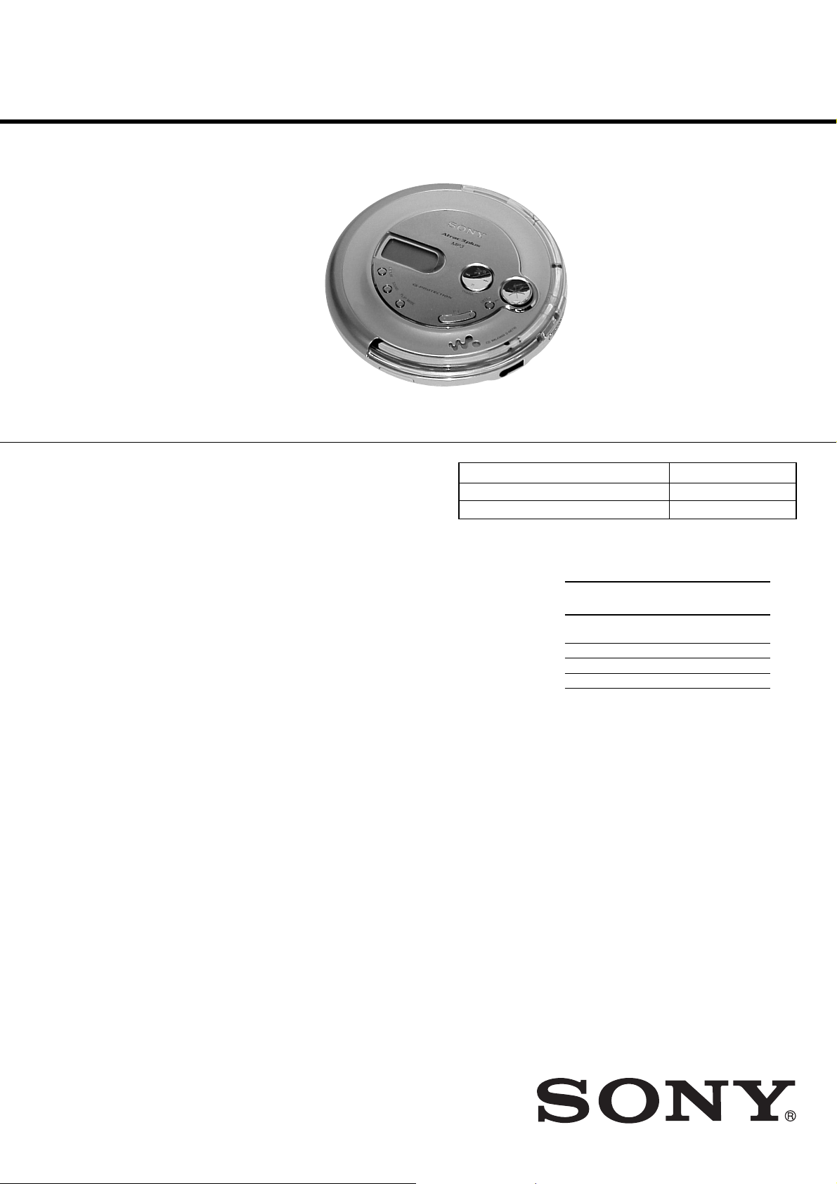
Photo : D-NE710
US Model
D-NE710/NE718CK
Canadian Model
D-NE711/NE718CK
AEP Model
UK Model
D-NE711/NE715
E Model
D-NE715
Austrarian Model
Chinese Model
D-NE715
Model Name Using Similar Mechanism NEW
CD Mechanism Type CDM-3325ER2
Optical Pick-up Name DAX-25E
System
Compact disc digital audio system
Laser diode properties
Material: GaAlAs
Wavelength: = 780 nm
Emission duration: Continuous
Laser output: Less than 44.6 µW
(This output is the value measured at a distance
of 200 mm from the objective lens surface on
the optical pick-up block with 7 mm aperture.)
D-A conversion
1-bit quartz time-axis control
Frequency response
20 - 20 000 Hz
307)
Output (at 4.5 V input level)
Line output (stereo minijack)
Output level 0.7 V rms at 47 kΩ
Recommended load impedance over 10 kΩ
Headphones (stereo minijack)
Approx.5 mW + Approx. 5 mW at 16 Ω
+1
dB (measured by JEITA CP-
–2
SPECIFICATIONS
Power requirements
For the area code of the model you
purchased, check the upper left side of the
bar code on the package.
•Sony NH-WM2AA rechargeable batteries:
1.2 V DC 2
•Two LR6 (size AA) batteries: 1.5 V DC 2
•AC power adaptor (DC IN 4.5 V jack):
U, US, CND, E92, MX,and TW
models: 120 V, 60 Hz
AEP, EE, and E13
models: 220 - 230 V, 50/60 Hz
UK model: 230 V, 50 Hz
AUS model: 240 V, 50 Hz
AEP, JE.W, E18, KR and EE8
models: 100 - 240 V, 50/60 Hz
HK model: 230 V, 50 Hz
CNA model: 220 V, 50 Hz
Battery life1 (approx. hours)
(When you use the CD player on a flat and stable
surface)
Playing time varies depending on how the CD
player is used.
•Abbreviation
AUS:Australian model
CHA: Chinese model
CND: Canadian model
E13 : 220 – 230 V AC area in E model
E18 : 100 – 240 V AC area in E model
E92 : 120 V AC area in E model
EE : East European model
MX : Mexican model
HK : Hong Kong model
KR : Korean model
When using two Sony alkaline batteries
LR6 (SG) (produced in Japan)
G-PROTECTION function
“1” “2”
Audio CD 55 50
ATRAC3plus files*
MP3 files*
*1 Measured value by the standard of JEITA
(Japan Electronics and Information Technology
Industries Association)
*2 When recorded at 48 kbps or 64 kbps
*3 When recorded at 128 kbps
Operating temperature
5°C - 35°C (41°F - 95°F)
Dimensions (w/h/d) (excluding
projecting parts and controls)
Approx. 136.0 28.7 136.0 mm
3
(5
⁄8 1 3⁄16 5 3⁄8 in.)
Mass (excluding accessories)
Approx. 199 g (7.1 oz.)
Design and specifications are subject to change
without notice.
2
3
95 95
85 85
PORTABLE CD PLAYER
9-877-311-03
2003G16-1
© 2003.07
Sony Corporation
Personal Audio Company
Published by Sony Engineering Corporation
D-NE710/NE711/NE715/NE718CK
TABLE OF CONTENTS
1. SERVICING NOTE ·························································· 3
2. GENERAL ··········································································4
3. DISASSEMBLY································································ 5
4. ELECTRICAL CHECKING ··········································· 8
5. DIAGRAMS········································································ 9
5-1. Block Diagram – MAIN Section (1/2) – ····················· 10
– MAIN Section (2/2) –··············································· 11
– Power Supply Section – ··········································· 12
5-2. Printed Wiring Board – MAIN Board (Side A) –······· 13
5-3. Printed Wiring Board – MAIN Board (Side B) –······· 14
5-4. Schematic Diagram – MAIN Board (1/4) – ···············15
5-5. Schematic Diagram – MAIN Board (2/4) – ···············16
5-6. Schematic Diagram – MAIN Board (3/4) – ···············17
5-7. Schematic Diagram – MAIN Board (4/4) – ···············18
5-8. IC Block Diagrams ······················································ 19
5-9. IC Pin Function Descriptions ······································ 22
6. EXPLODED VIEWS ······················································ 27
7. ELECTRICAL PARTS LIST ······································· 30
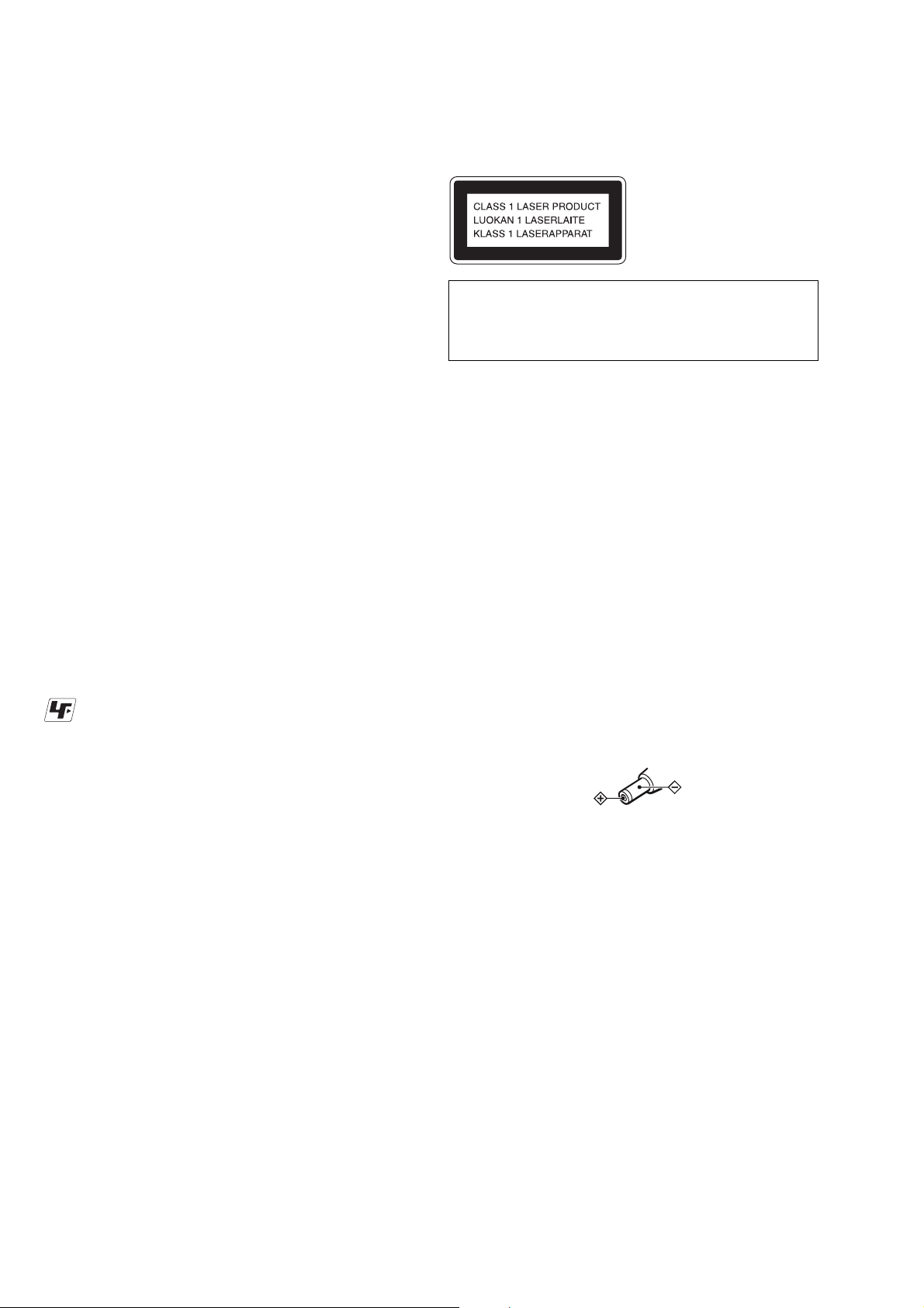
This appliance is classified as a CLASS 1 LASER product.
The CLASS 1 LASER PRODUCT MARKING is located on
the rear exterior.
CAUTION
Use of controls or adjustments or performance of procedures
other than those specified herein may result in hazardous
radiation exposure.
Flexible Circuit Board Repairing
•Keep the temperature of the soldering iron around 270 ˚C during repairing.
• Do not touch the soldering iron on the same conductor of the
circuit board (within 3 times).
• Be careful not to apply force on the conductor when soldering
or unsoldering.
Notes on chip component replacement
•Never reuse a disconnected chip component.
• Notice that the minus side of a tantalum capacitor may be damaged by heat.
Unleaded solder
Boards requiring use of unleaded solder are printed with the leadfree mark (LF) indicating the solder contains no lead.
(Caution: Some printed circuit boards may not come printed with
the lead free mark due to their particular size.)
: LEAD FREE MARK
Unleaded solder has the following characteristics.
• Unleaded solder melts at a temperature about 40°C higher than
ordinary solder.
Ordinary soldering irons can be used but the iron tip has to be
applied to the solder joint for a slightly longer time.
Soldering irons using a temperature regulator should be set to
about 350°C.
Caution: The printed pattern (copper foil) may peel away if the
heated tip is applied for too long, so be careful!
• Strong viscosity
Unleaded solder is more viscous (sticky , less prone to flo w) than
ordinary solder so use caution not to let solder bridges occur such
as on IC pins, etc.
• Usable with ordinary solder
It is best to use only unleaded solder but unleaded solder may
also be added to ordinary solder.
Notes on the power source
Disconnect all power sources when the CD player is not used for a long time.
On AC power adaptor
• Use only the AC power adaptor supplied.
If your CD player is not supplied with the one, use the AC-E45HG AC
power adaptor. Do not use any other AC power adaptor. It may cause a
malfunction.
Polarity of the plug
• Do not touch the AC power adaptor with wet hands.
• Connect the AC power adaptor to an easily accessible AC outlet. Should
you notice an abnormality in the AC power adaptor, disconnect it from
the AC outlet immediately.
SAFETY-RELATED COMPONENT WARNING!!
COMPONENTS IDENTIFIED BY MARK 0 OR DOTTED LINE WITH
MARK 0 ON THE SCHEMATIC DIAGRAMS AND IN THE PARTS
LIST ARE CRITICAL TO SAFE OPERATION. REPLACE THESE
COMPONENTS WITH SONY PARTS WHOSE PART NUMBERS
APPEAR AS SHOWN IN THIS MANUAL OR IN SUPPLEMENTS
PUBLISHED BY SONY .
2
ATTENTION AU COMPOSANT AYANT RAPPORT
À LA SÉCURITÉ!
LES COMPOSANTS IDENTIFÉS P AR UNE MARQUE 0 SUR LES
DIAGRAMMES SCHÉMA TIQUES ET LA LISTE DES PIÈCES SONT
CRITIQUES POUR LA SÉCURITÉ DE FONCTIONNEMENT. NE
REMPLACER CES COMPOSANTS QUE PAR DES PIÈSES SONY
DONT LES NUMÉROS SONT DONNÉS DANS CE MANUEL OU
DANS LES SUPPÉMENTS PUBLIÉS PAR SONY.
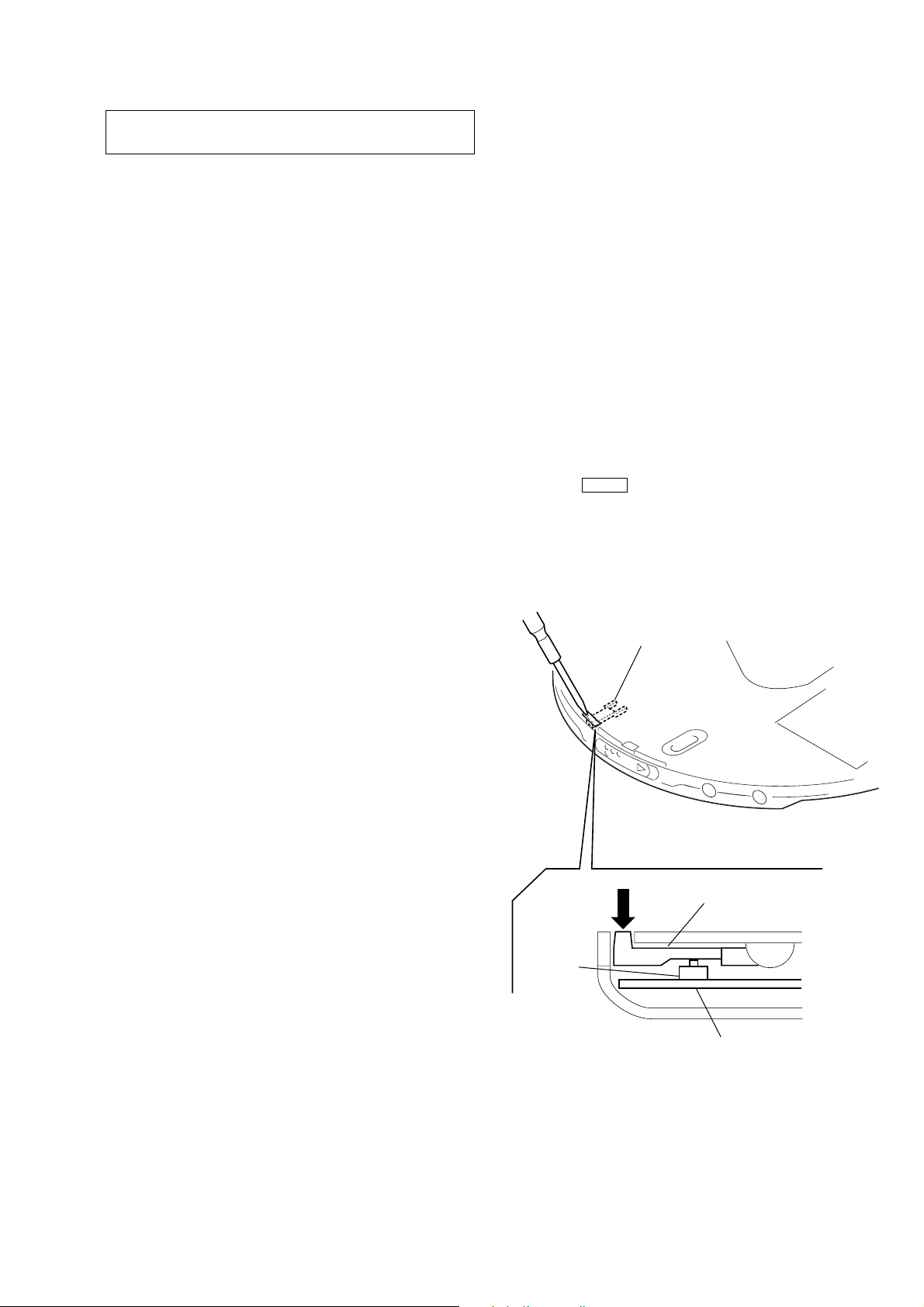
SECTION 1
S801
detection lever
detection lever
MAIN board
SERVICING NOTE
D-NE710/NE711/NE715/NE718CK
NOTES ON HANDLING THE OPTICAL PICK-UP
BLOCK OR BASE UNIT
The laser diode in the optical pick-up block may suffer electrostatic
breakdown because of the potential difference generated by the
charged electrostatic load, etc. on clothing and the human body.
During repair, pay attention to electrostatic breakdown and also use
the procedure in the printed matter which is included in the repair
parts.
The flexible board is easily damaged and should be handled with
care.
NOTES ON LASER DIODE EMISSION CHECK
The laser beam on this model is concentrated so as to be focused on
the disc reflective surface by the objective lens in the optical pickup block. Therefore, when checking the laser diode emission,
observe from more than 30 cm away from the objective lens.
BEFORE REPLACING THE OPTICAL PICK-UP BLOCK
Please be sure to check thoroughly the parameters as par the “Optical
Pick-Up Block Checking Procedures” (Part No.: 9-960-027-11)
issued separately before replacing the optical pick-up block.
Note and specifications required to check are given below.
• FOK output: IC601 yg pin
When checking FOK, remove the lead wire to disc motor.
• RF signal P-to-P value: 0.4 to 0.6 Vp-p
LASER DIODE AND FOCUS SEARCH OPERATION
CHECK
During normal operation of the equipment, emission of the laser
diode is prohibited unless the upper lid is closed while turning ON
the S801. (push switch type)
The following checking method for the laser diode is operable.
• Method:
Emission of the laser diode is visually checked.
1. Open the upper lid.
2. With a disc not set, turn on the S801 with a screwdriver ha ving a
thin tip as shown in Fig.1.
3. Press the > B button.
4. Observing the objective lens, check that the laser diode emits
light.
When the laser diode does not emit light, automatic power control
circuit or optical pickup is faulty.
In this operation, the objective lens will move up and down 4
times along with inward motion for the focus search.
Fig. 1 Method to push the S801
3
D-NE710/NE711/NE715/NE718CK
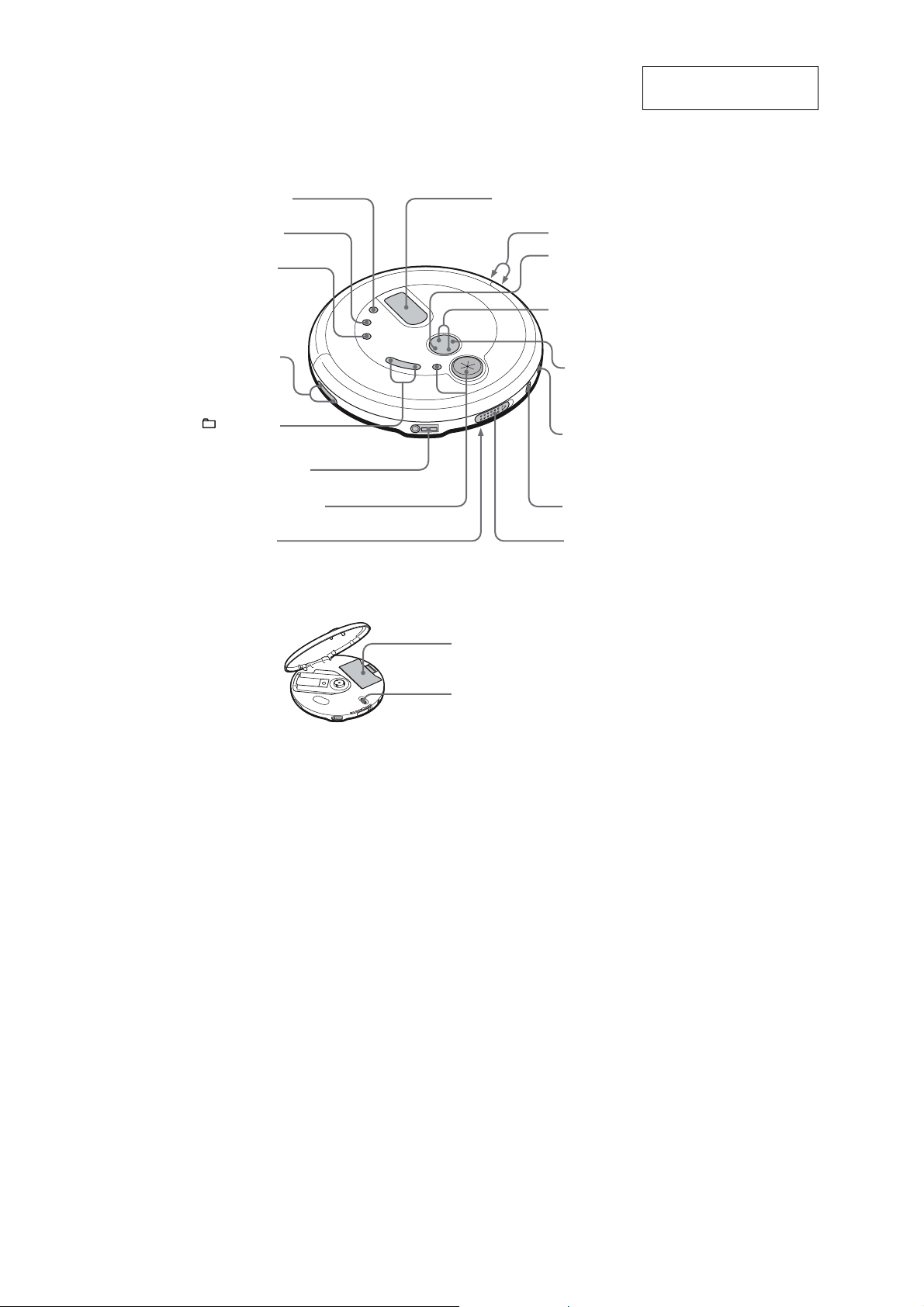
CD player (front)
SECTION 2
GENERAL
This section is extracted
from instruction manual.
1 DISPLAY button
(pages 23, 24)
2 SOUND button
(pages 24, 25)
3 PLAY MODE
(play mode/repeat)
button (pages 16 - 19,
21, 22)
4 VOL (volume)
+*/– buttons
(page 11)
5 +/– buttons
(page 12)
6 i (headphones) jack
(page 11)
7 Jog dial•ENTER button
(pages 16, 20 - 22)
8 HOLD switch
(page 25)
*The button has a tactile dot.
CD player (inside)
9 Display
(pages 13, 16, 19 - 21, 23 - 25)
q; Strap holes
qa x (stop)/CHARGE
button
(pages 12, 25, 27)
qs ./> (AMS/
search) buttons
(pages 12, 16, 19, 21)
qd u* (play/pause)
button
(pages 11, 12, 16,
18, 19, 21)
qf DC IN 4.5 V
(external power
input) jack
(pages 27, 28)
qg LINE OUT jack
(page 26)
qh OPEN switch
(page 11)
qj Battery compartment
(pages 11, 28)
qk G-PROTECTION
switch (page 23)
4
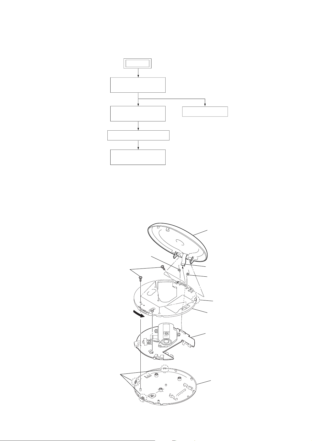
DISASSEMBLY
)
Note : Disassemble the unit in the order as shown below.
SET
CABINET MIDDLE ASSY,
UPPER LID ASSY
D-NE710/NE711/NE715/NE718CK
SECTION 3
CD MECHANISM
(CDM-3325ER2)
TURN TABLE MOTOR ASSY
OPTICAL PICK-UP
(DAX-25E)
Note : Follow the disassembly procedure in the numerical order given.
3-1. Cabinet Middle Assy, Upper Lid Assy
3
spring full open (L)
SWITCH UNIT ASSY
9
upper lid assy
4
seven screws (B2)
1
Slide open knob to
open the lid.
5
three claws
8
flexible cable 22p (CN801
2
spring full open (R)
6
claw
7
cabinet middle assy
q;
MAIN board,
CD mechanism
cabinet lower sub assy
5
D-NE710/NE711/NE715/NE718CK
)
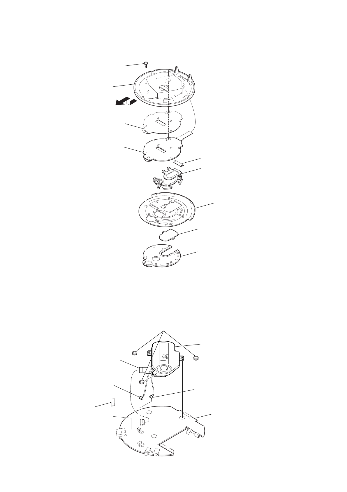
3-2. Switch Unit Assy
1
eight screws
2
upper lid
3
sheet cover
4
switch unit assy
5
sheet copper
6
button (operate
3-3. CD Mechanism (CDM-3325ER2)
4
flexible board
(15P) (CN501)
5
three insulators
7
ornament
8
LCD window
9
cover
6
CD mechanism
(CDM-3325ER2 )
2
connector (CN502)(4P)
1
sheet
3
connector (CN503)(2P)
7
MAIN board
6
y
3-4. Turn Table Motor Assy
1
three screws
(B1.7
D-NE710/NE711/NE715/NE718CK
×
4)
2
turn table motor ass
(spindle) (M901)
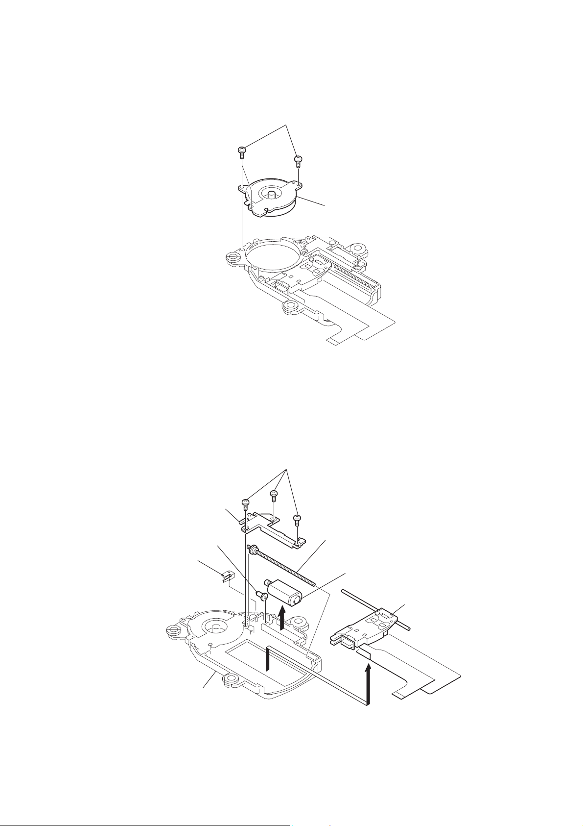
3-5. Optical Pick-up (DAX-25E)
2
gear cover
4
gear B
6
sled spring
1
three screws
(B1.7
×
4)
5
feed screw assy
3
motor assy
(sled) (M902)
7
optical pick-up
(DAX-25E)
chassis
7
D-NE710/NE711/NE715/NE718CK
ELECTRICAL CHECKING
SECTION 4
The CD section adjustments are done automatically in this set.
In case of operation check, confirm that focus bias.
Precautions for Check
1. Perform check in the order given.
2. Use YEDS-18 disc (Part No.: 3-702-101-01) unless otherwise
indicated.
3. Power supply voltage requirement : DC4.5 V in DC IN jack.
(J401)
VOLUME button : Minimum
AVLS : OFF
HOLD switch : OFF
G-PROTECTION switch : 1
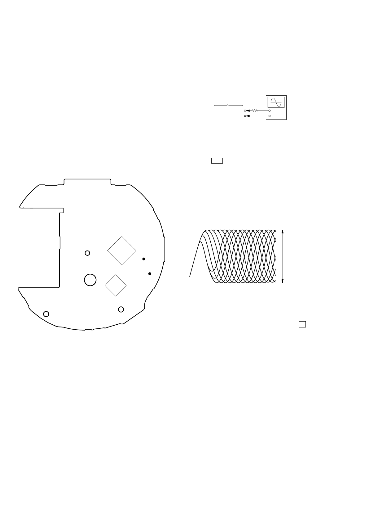
Checking Location:
– MAIN board (Side B) –
RF Level Check
Condition:
• Hold the set in horizontal state.
Connection:
oscilloscope
(AC range)
MAIN board
TP601 (RF)
TP415(GND)
2 k
Ω
+
–
Procedure:
1. Connect the oscilloscope to the test points TP601 (RF) and
TP415 (GND) on the MAIN board.
2. Set a disc. (YEDS-18)
3. Press the u button.
4. Check the oscilloscope waveform is as shown below.
A good eye pattern means that the diamond shape (◊) in the
center of the waveform can be clearly distinguished.
RF Signal reference Waveform (Eye Pattern)
VOLT/DIV : 100 mV (With the 10:1 probe in use)
TIME/DIV : 500 ns
IC601
IC403
TP601(RF)
TP415
(GND)
RF level
0.45 to 0.65 Vp-p
To watch the eye pattern, set the oscilloscope to AC range and
increase the vertical sensitivity of the oscilloscope for easy watching.
5. Stop revolving of the disc motor by pressing the x button.
8
SECTION 5
DIAGRAMS
NOTE FOR PRINTED WIRING BOARDS AND SCHEMATIC DIAGRAMS
D-NE710/NE711/NE715/NE718CK
Note on Printed Wiring Board
• X : parts extracted from the component side.
• Y : parts extracted from the conductor side.
• : Pattern from the side which enables seeing.
(The other layers' patterns are not indicated.)
Caution:
Pattern face side: Parts on the pattern face side seen from
(Side A) the pattern face are indicated.
Parts face side: Parts on the parts face side seen from
(Side B) the parts face are indicated.
• MAIN board is multi-layer printed board. However, the patterns of intermediate-layer have not been included in the diagram.
Note on Schematic Diagram:
• All capacitors are in µF unless otherwise noted. pF: µµF 50 WV
or less are not indicated except for electrolytics and tantalums.
• All resistors are in Ω and 1/
fied.
•%: indicates tolerance.
f
•
• C : panel designation.
• A : B+ Line.
•Total current is measured with CD installed.
•Power voltage is dc 4.5 V and fed with regulated dc power supply
•Voltages and waveforms are dc with respect to ground in playback
•Voltages are taken with a VOM (Input impedance 10 MΩ).
•Waveforms are taken with a oscilloscope.
• Circled numbers refer to waveforms.
• Signal path.
•Abbreviation
: internal component.
Note:
The components identified by
mark 0 or dotted line with mark
0 are critical for safety.
Replace only with part number
specified.
from DC IN jack (J401).
mode.
no mark : CD PLAY
Voltage v ariations ma y be noted due to normal production toler-
ances.
Voltage v ariations ma y be noted due to normal production toler-
ances.
J : CD PLAY (ANALOG OUT)
AUS:Australian model
CH : Chinese model
CND: Canadian model
E18 : 100 – 240 V AC area in E model
EE : East European model
HK : Hong Kong model
KR : Korean model
MX : Mexican model
4
W or less unless otherwise speci-
Note:
Les composants identifiés par
une marque 0 sont critiques
pour la sécurité.
Ne les remplacer que par une
pièce portant le numéro spécifié.
• WA VEFORMS
1 IC601 if RFAC
100mV/DIV, 400ns/DIV
600 mVp-p
5 IC701 e; XTAL
1V/DIV, 20ns/DIV
3.1 Vp-p
44ns
2 IC601 rk XTAO
1V/DIV, 20ns/DIV
59ns
2.4 Vp-p
✩ When IC803 is damaged, replace the MAIN board.
3 IC801 wk XIN
1V/DIV, 40ns/DIV
1.8 Vp-p
118ns
4 IC403 ef SYNC
1V/DIV, 2us/DIV
5.7us
2.5 Vp-p
99
D-NE710/NE711/NE715/NE718CK
5-1. Block Diagram – MAIN Section (1/2) –
DETECTOR
A
B
RF
E
F
VCC
OPTICAL PICK-UP BLOCK
DAX-25E
LASER DIODE
PD
A
PD
LD
B
(FOCUS)
2-AXIS
DEVICE
(TRACKING)
M901
SPINDLE
MOTOR
V
U
W
A
B
RF
E
F
VCPU
OPGSW
OPSTB
LD
M902
SLED
M
MOTOR
U1
79
V1
78
W1
77
COM
26
U
2
V
4
W
6
+
+
+
MOTOR
DRIVER
IC403 (1/3)
FOCUS/TRACKING COIL DRIVER
SLED MOTOR DRIVER
FO1
52
RO1
50
FO3
44
42
48
46
CONTROLLER,
RO3
H BRIDGE DRIVER
FO2
RO2
IC403 (2/3)
SPINDLE MOTOR DRIVER
CONTROL
CIRCUIT
RI1
RI3
RI2
IC601
RF AMP,
DIGITAL SIGNAL PROCESSOR,
DIGITAL SERVO PROCESSOR,
D-RAM CONTROLLER
A
92
B
91
RFDC
88
RFAC
84
E
89
F
90
FI1
56
55
FI3
60
59
FI2
58
57
PWM
SOFTPWM(APWM)
BRA
72
73
70
FG
74
TAP 403
100
104
103
102
SFDR
SRDR
99
FFDR
96
FRDR
95
TFDR
98
TRDR
97
C176
MDP
MDS
SCOR_O
27
FG_I
10
SCOR_I
HG-XSTB_O
HG-GUP_O
12
13
WDCK_O
WFCK
MDS
XTAO
XTAI
RFAC
MDP
XSOE_I
SENS_O
R8M
XLAT_I
CLOCK_I
SCOR_O
SDTO_I
RFDC
SFDR
SRDR
FFDR
FRDR
TFDR
TRDR
E
F
B
A
SIGNAL
PROCESSOR
BLOCK
SDTO_I
SENS_O
CLOCK_I
858887838486
MSDTI0_I
MSDTO0_O
DIGITAL
MEMORY
CONTROLLER,
BASS BOOST
BLOCK
SERVO
BLOCK
XSOE_I
XLAT_I
232021
XLAT0_O
MSCK0_O
WDCK_O
R8M
32 65
2422
26
28
XIN
XSOE_O
IC801 (1/3)
SYSTEM CONTROLLER
OUT
FOK
LPF
FOK
52
FOK_I
DOUT
D0-D3
A0-A10
XRAS
XWE
XCAS
XTAI
XTAO
AOUT1
AOUT2
PCMD_I
PCMD_O
LRCK_I
LRCK_O
BCK_I
BCK_O
XRDE
LRMU
XRST_I
25
7
62
4, 3, 6, 5
116 – 113, 17 – 15, 13 – 11, 117
1
2
9
47
48
51
56
109
108
107
106
111
110
18
61
28
SYSM_I
AMUTE_O
16.9344MHz
PCMD_I
PCMD_O
LRCK_I
LRCK_O
BCK_I
BCK_O
XRDE
IC602
D-RAM
D0 – D3A0 – A10
2, 3, 24, 25
9 – 12, 15 – 19, 21, 8
5
XRAS
4
XWE
23
XCAS
X601
AOUTL,
AOUTR
LRMU
XRST
G
F
H
I
• SIGNAL PATH
: CD PLAY (ANALOG OUT)
SYNC
C
MSCK
D
MSDTO
E
1010
– MAIN Section (2/2) –
D-NE710/NE711/NE715/NE718CK
AOUTR
G
AOUTL
Q301
MUTING
J302
J301
LINE OUT
i
IC303
HEADPHONE AMP
AOUTL
AOUTR
Q302
LINE MUTE
CONTROL SWITCH
LRMU
H
IC302
ATT SWITCH
21
7
54
3
XRST
I
14
15
19
20
17
LIN
RIN
MUTE
PWRSW
BEEP
MT SW
PW SW
BEEP
LOUT
ROUT
8
6
VCPU 2.0V
VCPU 2.0V
4
3
S806
S807
+
VOL
–
2
1
TSB
RMKEY
GND
Q801
36
Q802
WAKE_I
AD-KEY3
98
31
TSB
97
AD-RMKEY
LCD-XRST_O
AD-KEY2
RE1_I
RE2_I
AD7
AD0
LCD_A0
XRD_O
XWR_O
SWITCH
&
14
15
44
51
69
71
72
73
LCD MODULE
DISPLAY
SOUND
PLAY MODE
ENTER
+
−
u
. >
(CHARGE)
x
• SIGNAL PATH
: CD PLAY (ANALOG OUT)
15
4
14
1
13
2
12
30
29
IC701
CDROM I/F
PI0
PCMD
PI2
LRCK
PI3
BCK
PF4
XTAL
EXTAL
PC3
PF2
PC0
PC2
PC1
65 8 77 6 9996
XRESET_INRST
6033
WAKEUP_K_OPF0
6634
REQ_IPF3
1137
SDXLAT_O
1742
36
38
41
40
HP_LIN_SEL_I
SDCLK_OSK19SDOUT_ODI20SDIN_IDO67EEP_CS_OCS
18
2 3 4 1
IC803
EEPROM
4
XRST_O
>
S803
HOLD
HOLD
OFF
H/P SW
LINEOUT_I
VCPU 2.0V VCPU 2.0V
BEEP_O
HOLD_I
40
IC801(2/3)
SYSTEM CONTROLLER
LID-SW_I
37
TAP802
(OPEN)
S801
(CD LID OPEN
DETECT)
ESP_I
39
VCPU 2.0V
AD-KEY1
S804
G-PROTECTION
2
1
F
PCMD_I
PCMD_O
LRCK_I
LRCK_O
BCK_I
BCK_O
XRDE
X701
22MHz
1111
 Loading...