

Sony DNE-510 Service manual
D-NE510/NE511/NE518CK
SERVICE MANUAL
Ver. 1.1 2005.06
Photo: D-NE518CK
SPECIFICATIONS
US Model
Canadian Model
D-NE510/NE518CK
AEP Model
UK Model
E Model
Australian Model
D-NE511/NE518CK
Model Name Using Similar Mechanism NEW
CD Mechanism Type CDM-3325ER2
Optical Pick-up Name DAX-25E
System
Compact disc digital audio system
Laser diode properties
Material: GaAlAs
Wav elength: λ = 780 nm
Emission duration: Continuous
Laser output: Less than 44.6 µW
(This output is the value measured at a distance
of 200 mm from the objective lens surface on
the optical pick-up block with 7 mm aperture.)
D-A conversion
1-bit quartz time-axis control
Frequency response
20 – 20,000 Hz dB
(measured by JEITA CP-307)
Output (at 4.5 V input level)
Headphones (stereo minijack)
Approx. 5 mW + Approx. 5 mW at 16 Ω
(Approx. 1.5 mW + Approx. 1.5 mW
at 16 Ω)*
*For the customers in Europe
Power requirements
For the area code of the model you
purchased, check the upper left side of the
bar code on the package.
• Two LR6 (size AA) batteries: 1.5 V DC × 2
• AC power adaptor (DC IN 4.5 V jack):
US/CND/E92/MX model: 120 V, 60 Hz
AEP/EE model: 220 – 230 V, 50/60 Hz
UK model: 230 V, 50 Hz
AUS model: 240 V, 50 Hz
E18 model: 100 – 240 V, 50/60 Hz
+1
–2
Battery life*1 (approx. hours)
(When you use the CD player on a flat and stable
surface)
Playing time varies depending on how the CD
player is used.
When using two Sony alkaline batteries
LR6 (SG) (produced in Japan)
Audio CD 50 45
ATRAC3plus files*
MP3 files*
*1 Measured value by the standard of JEITA
(Japan Electronics and Information Technology
Industries Association)
*2 When recorded at 48 kbps or 64 kbps
*3 When recorded at 128 kbps
Operating temperature
5°C – 35°C (41°F – 95°F)
Dimensions (w/h/d) (excluding
projecting parts and controls)
Approx. 136.0 × 26.3 × 156.3 mm
(5 3 ⁄8 × 1 1 ⁄16 × 6 1 ⁄4 in.)
Mass (excluding accessories)
Approx. 202 g (7.2 oz.)
Supplied accessories
D-NE510
Headphones (1) (US)
Earphones (1) (CND)
CD-ROM (SonicStage Simple Burner) (1)
User’s guide for SonicStage Simple Burner (1)
G-PROTECTION function
“1” “2”
2
3
80 80
75 75
D-NE511
AC power adaptor (1)
Earphones (1)
CD-ROM (SonicStage Simple Burner) (1)
User’s guide for SonicStage Simple Burner (1)
D-NE518CK
AC power adaptor (1)
Headphones (1) (US)
Earphones (1) (Except US)
Rotary commander (RM-MC25C) (1)
Car battery cord (1)
Car connecting pack (1)
Velcro tapes for the CD player (2)
Velcro tape for the rotary commander (1)
CD-ROM (SonicStage Simple Burner) (1)
User’s guide for SonicStage Simple Burner (1)
For US customers
The AC power adaptor supplied is not intended to
be serviced. Should the AC power adaptor cease to
function in its intended manner, during the warranty
period, the adaptor should be returned to your nearest Sony Service Center or Sony Authorized Repair
Center for replacement, or after warranty period, it
should be discarded.
Design and specifications are subject to change
without notice.
•Abbreviation
CND : Canadian model
E18 : AC 100 – 240V area in E model
E92 : AC 120V area in E model
EE : East European model
AUS: Australian model
MX : Mexican model
9-877-188-02
2005F04-1
© 2005.06
PORTABLE CD PLAYER
Sony Corporation
Personal Audio Group
Published by Sony Engineering Corporation
1

D-NE510/NE511/NE518CK
Flexible Circuit Board Repairing
• Keep the temperature of the soldering iron around 270°C during
repairing.
• Do not touch the soldering iron on the same conductor of the
circuit board (within 3 times).
• Be careful not to apply force on the conductor when soldering
or unsoldering.
Notes on Chip Component Replacement
• Never reuse a disconnected chip component.
• Notice that the minus side of a tantalum capacitor may be
damaged by heat.
Music sources playable on this CD player
You can play the following 3 music sources on this CD player:
• Audio CDs
•ATRAC3plus/ATRAC3 format files
• MP3 files
Usable disc formats
You can use ISO 9660 Level 1/2, Joliet extension format discs only .
ATRAC3plus and ATRAC3
“ATRAC3plus,” which stands for “Adaptive Transform Acoustic
Coding3plus” is audio compression technology, de veloped from the
ATRAC3 format. Though the ATRAC3plus format can compress
music content to about 1/20 of its original size, you can still enjoy
high quality sound. The available transfer bit rates are 64 kbps and
48 kbps.
TABLE OF CONTENTS
1. SERVICE NOTE................................................................. 3
2. GENERAL
Locating the controls ............................................................... 4
3. DISASSEMBLY
3-1. Lid (Upper) Assy................................................................. 5
3-2. Cabinet (Front) Assy ...........................................................6
3-3. Main Board ......................................................................... 6
4. ELECTRICAL ADJUSTMENTS
4-1. Focus Bias Check ................................................................7
5. DIAGRAMS
5-1. IC Pin Descriptions ............................................................. 8
5-2. Block Diagram –CD Section–........................................... 15
5-3. Block Diagram –Audio Section– ...................................... 16
5-4. Block Diagram –Power Supply Section–.......................... 17
5-5. Printed Wiring Board –Main Section– ..............................18
5-6. Schematic Diagram –Main Section (1/2)– ......................... 20
5-7. Schematic Diagram –Main Section (2/2)– ......................... 21
5-8. IC Block Diagrams............................................................ 22
6. EXPLODED VIEWS
6-1. Cabinet (Front) Section .....................................................23
6-2. Main Board Section .......................................................... 24
6-3. CD Mechanism Deck Section (CDM-3325ER2) ..............25
“ATRAC3,” which stands for “Adaptive Transform Acoustic
Coding3” is audio compression technology that satisfies the demand
for high sound quality and high compression rates. The ATRAC3
format can compress music content to about 1/10 of their original
size, which contributes to reduction of the media volume. The
available transfer bit rates are 132 kbps, 105 kbps and 66 kbps.
The usable number of groups and files
• Maximum number of groups: 255
• Maximum number of files: 999
For details, refer to the supplied booklet “SonicStage Simple Burner . ”
MP3 files
MP3, which stands for MPEG-1 Audio Layer3, a standard for audio
files compression supported by the Motion Picture Experts Group,
an ISO (International Organization for Standardization) working
group, enables compression of audio files to about 1/10 of the data
size of a standard compact disc. Since the MP3 encoding algorithm
is public, there are various encoders/decoders that are compliant
with this standard, including freeware that is av ailable for no charge.
Thus, the MP3 standard is widely used in the computer field.
7. ELECTRICAL PARTS LIST......................................... 26
SAFETY-RELATED COMPONENT WARNING!!
COMPONENTS IDENTIFIED BY MARK 0 OR DOTTED LINE
WITH MARK 0 ON THE SCHEMATIC DIAGRAMS AND IN
THE PARTS LIST ARE CRITICAL TO SAFE OPERATION.
REPLACE THESE COMPONENTS WITH SONY P ARTS WHOSE
PART NUMBERS APPEAR AS SHOWN IN THIS MANUAL OR
IN SUPPLEMENTS PUBLISHED BY SONY.
2
ATTENTION AU COMPOSANT AYANT RAPPORT
À LA SÉCURITÉ!!
LES COMPOSANTS IDENTIFIÉS P AR UNE MARQUE 0 SUR LES
DIAGRAMMES SCHÉMATIQUES ET LA LISTE DES PIÈCES
SONT CRITIQUES POUR LA SÉCURITÉ DE FONCTIONNEMENT .
NE REMPLACER CES COMPOSANTS QUE PAR DES PIÈCES
SONY DONT LES NUMÉROS SONT DONNÉS DANS CE MANUEL
OU DANS LES SUPPLÉMENTS PUBLIÉS PAR SONY.
SECTION 1
SERVICE NOTE
D-NE510/NE511/NE518CK
NOTES ON HANDLING THE OPTICAL PICK-UP BLOCK
OR BASE UNIT
The laser diode in the optical pick-up block may suffer electrostatic breakdown because of the potential difference generated by
the charged electrostatic load, etc. on clothing and the human body .
During repair, pay attention to electrostatic breakdown and also
use the procedure in the printed matter which is included in the
repair parts.
The flexible board is easily damaged and should be handled with
care.
Precautions for Checking Emission of Laser Diode
Laser light of the equipment is focused by the object lens in the
optical pick-up so that the light focuses on the reflection surface
of the disc. Therefore, be sure to keep your eyes more then 30 cm
apart from the object lens when you check the emission of laser
diode.
Before Replacing the Optical Pick-Up Block
Please be sure to check throughly the parameters as par the “Optical Pick-Up Block Checking Procedures” (Part No.: 9-960-027-
11) issued separately before replacing the optical pick-up block.
Note and specifications required to check are given below.
• FOK output : IC601 yg pin (or TP618 (FOK))
When checking FOK, remove the lead wire to disc motor.
• RF signal P-to-P value : 0.45 ± 0.1 Vp-p
• The repairing grating holder is impossible.
Laser Diode Checking Methods
During normal operation of the equipment, emission of the laser
diode is prohibited unless the upper lid is closed while turning ON
the S820. (push switch type)
The following two checking methods for the laser diode are
operable.
• Method:
Emission of the laser diode is visually checked.
1. Open the upper lid.
2. With a disc not set, turn on the S820 with a screwdriver ha ving a
thin tip as shown in Fig.1.
or TAP805 is shorted as shown in Fig.2.
Note: Do not push the detection lever strongly , or it may be bent
or damaged.
3. Press the N X button.
4. Observing the objective lens, check that the laser diode emits
light.
When the laser diode does not emit light, automatic power
control circuit or optical pick-up is faulty.
In this operation, the objective lens will move up and down 5
times along with inward motion for the focus search.
S820
– MAIN BOARD – (SIDE B)
C853
TP422
TJ402
R467
C447
R438
R484
C436
C434
FB403
R487
– MAIN BOARD – (SIDE A)
FB402
FN406
CN601
15
FB404
1
FB405
R606
R650
R301C307
R302
C309
C308
detection lever
detection lever
R612
R101R201
TP942
TP941
TJ503
R495
TJ501
TJ502
R498
S820
Fig. 1
FB409
main board
C107
C103
R102
C207
C203
R202
TP939
TP940
TP826
TJ406(VCPU)
SL806
132412
R303
R111
R211
S820
(OPEN/CLOSE)
C808
R871
TP820
FB410
R427
IC301
L301
C305
C306
1
TP930
R943
R806
S804
TP934
TP933
TP932
R947
R948
R946
TP929
R945
R867
TP911
C303
C302
TAP805
TP910
TAP805
Fig. 2
C424
R436
R477C427
C442
3
D-NE510/NE511/NE518CK
Getting started
Locating the controls
For details, see pages in parentheses.
SECTION 2
GENERAL
This section is extracted
from instruction manual.
CD player (front)
1 i (headphones)
jack (pages 11,
24, 29)
2 VOL (volume)
+*/– buttons
(page 11)
3 OPEN button
(page 11)
4 +/–
buttons
(page 12)
5 P MODE/
(play mode/repeat)
button (pages 16 - 19)
6 DISPLAY button
(pages 21, 22)
7 HOLD switch
(page 23)
8 JOG DIAL/
ENTER (pages 16, 20)
*The button has a tactile dot.
CD player (inside)
Getting started
9 Display
(pages 13, 16, 19 - 23)
q; SOUND button
(pages 22, 23)
qa Strap holes
qs DC IN 4.5 V
(external power
input) jack
(pages 11, 24)
qd x (stop) button
(pages 12, 23)
qf u* (play/pause) button
(pages 11, 12, 16, 18, 19)
qg ./> (AMS/search)
buttons (pages 12, 16, 19)
qh G-PROTECTION
switch (page 21)
qj Battery compartment
(page 27)
Rotary commander
qk u (play/pause) button
(pages 12, 18, 19)
ql .(AMS/search)•
> (AMS/search)
control
(pages 12, 19)
w; Jack for connecting a car
connecting pack (page 24)
Note
The supplied rotary commander should be used with this player only.
(D-NE518CK only)
(Continued)
9-GB
wa x (stop) button
(pages 12, 23)
ws +/– control
Push down and turn.
(page 12)
4
SECTION 3
1
claws
2
lid (upper) assy
DISASSEMBLY
• The equipment can be removed using the following procedure.
SET
3-1. LID (UPPER) ASSY
(Page 5)
3-2. CABINET (FRONT) ASSY
(Page 6)
3-3. MAIN BOARD
(Page 6)
Note : Follow the disassembly procedure in the numerical order given.
3-1. LID (UPPER) ASSY
D-NE510/NE511/NE518CK
5
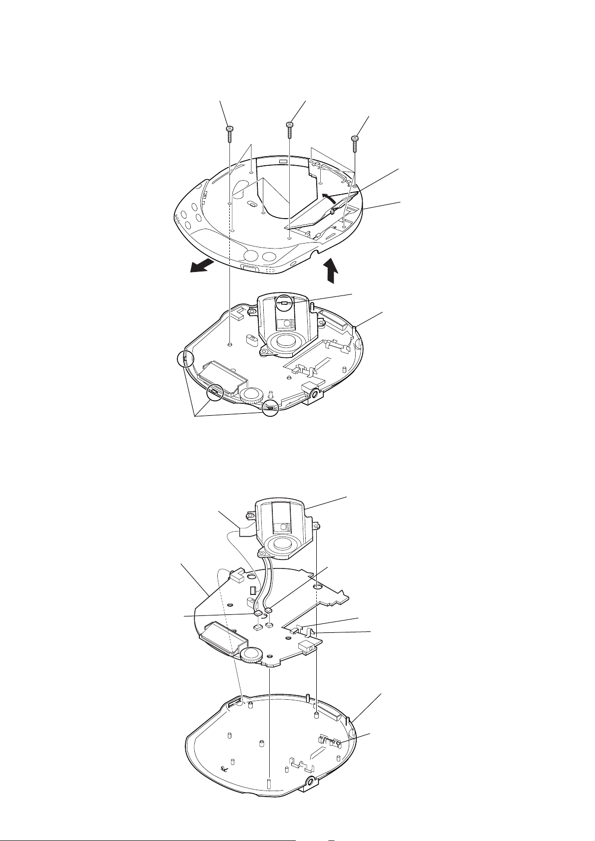
D-NE510/NE511/NE518CK
y
3-2. CABINET (FRONT) ASSY
7
4
screws (B 2)
3
screws (B 2)
1
8
5
claw
2
screws (B 2)
9
boss
battery case lid
cabinet (front) ass
3-3. MAIN BOARD
6
5
MAIN board
2
CN402
claws
3
CN601
4
MD assy
1
CN401
battery terminal plate (+)
battery terminal plate (–)
cabinet (rear) sub assy
battery link terminal
6
SECTION 4
ELECTRICAL ADJUSTMENTS
CD section adjustments are done automatically in this set.
In case of operation check, confirm that focus bias.
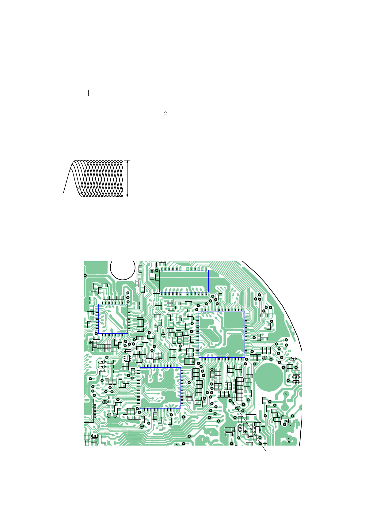
4-1. FOCUS BIAS CHECK
1. Connect the oscilloscope between TJ601 (RF) and GND on
main board.
2. Insert the disc (YEDS-18). (Part No. : 3-702-101-01)
3. Press the N X button.
4. Confirm that the oscilloscope waveform is as shown in the
figure below. (eye pattern)
A good eye pattern means that the diamond shape ( ) in the
center of the waveform can be clearly distinguished.
• RF signal reference waveform (eye pattern)
VOLT/DIV : 20 mV (10 : 1 probe in use)
TIME/DIV : 500 nS
RF level :
0.45 ± 0.1 Vp-p
D-NE510/NE511/NE518CK
When observing the eye pattern, set the oscilloscope for AC range
and raise vertical sensitivity.
Test Points:
— MAIN BOARD — (SIDE B)
L603
R715
TP954
R719
13 1
C622
R718
TP709
TP710
TP852
TP824
TP851
C414
C412
R706
R707
R726
TP711
CN807
R401
C701
FB701
C705
D802
D801
Q802
D404
R409
R402
R725
R729
TP811
L701
R708
C706
R720
TP812
TP823
C707
C704
32
33
48
E C B
TP804
SL804
X701
R731
R710
R709
L406
R829
R830
R831
R897
R906
R914
C711
IC701
R913
SL803
L409
R721
R733
R836
R835
TP805
R908
R912
SL802
C713
R711
Q801
D803
C814
TP713
C712
R825
R827
TP802
R842
TP808
R822
R717
TP702
TP701
TP703
C719
1
R716
716
C715
C716
C717
C718
1
6449
TP716
R723
TP715
C811
TP712
R832
TP714
R821R828
R811
R826
C B E
E B C
C812
100
1
C899
TP803
C813
25
TP810
VDR803
26 50
TP809
R823
C898
R837 R820
SL801
C623
14 26
R730
VDR609
R630
VDR608
R639
VDR607
R640
TP727
R645
R886
SL805
TP729
TP730
R887
C896
IC801
R971
R840
R844
R843
TP831
R819
VDR606
R641
R642
C628
VDR601
VDR806
R640
R816
R817
R846
R649
C626
TP951
TP813
R845
VDR605
R643
C604
FB601
76
75
51
TP821
IC603
L602
C602
C619
VDR604
VDR603
C627
C621
TP818
TP648
TP953
FB602
C697
C696
TP952
R636
TP612
X601
R613
R614
C620
R897
R853
TJ801
(TEST)
R611
R934
R935
R933
TP608
VDR610
60
R877
R847
R850
R911
R814
R949
30
31
61
TP615
TP619
TP606
TP608
TP616
TP624
TP623
TP653
TP646
TP617
TP620
R849
TP618
TP604
TP625
TP622
TP615
C624
TP647
TP602
IC601
R620
R619
R617
R618
C605
TP621
TP651
TP645
TP603
C607
C606
R621
C608
R625
R624
R623
TJ601
TJ602
C631
C632
C612
R663
R622
SL602
C609
TP949
VDR612
C699
R627
R630
R626C613
C614
R629
R626
R662
TP620
D601
TP652
TP642
TP644
TP643
R637
TP640
R634
TP914
C603
R608
R616 R615
R607
C618
C617
R604
SL601
VDR307
R601
EC B
Q601
TJ603
FB101
R635
TJ101
R609
C630
R605
TP630
FB305
TP603
TP638
TP635
TP301
TJ301
FB201
VDR308
TP633
TP632
TP347
VDR306
KAKA
TP946
TP631
TJ306
TP636
TP634
C318
R312
TJ201
D301
TP302
R316
C301
D308
1
TP641
120
TP637
TP960
90
91
C614
TP946
TP629
C611
C601
R633
R632
R603
R602
TP627
TP626
L601
C615
C610
R610 R670
R699
R631
TJ601 (RF)
7

D-NE510/NE511/NE518CK
SECTION 5
DIAGRAMS
5-1. IC PIN DESCRIPTIONS
• IC601 CXD3048R (RF AMP, DIGITAL SIGNAL PROCESSOR, DIGITAL SERVO PROCESSOR, D-RAM CONTROLLER)
Pin No. Pin Name I/O Pin Description
1 XRAS O Low address strobe signal output to the D-RAM
2 XWE O Data input enable signal output to the D-RAM
3 to 6 D1, D0, D3, D2 I/O Two-way data bus with the D-RAM
7 DCLK O Not used (open)
8 DCKE O Not used (open)
9 XCAS O Column address strobe signal output to the D-RAM
10 WFCK/DQM O Not used (open)
11 to 13 A9 to A7 O Address signal output to the D-RAM
14 DVSS — Ground
15 to 17 A6 to A4 O Address signal output to the D-RAM
18 XRDE I D-RAM read enable signal input
19 VDD0 — Power supply
20 CLOK I Serial data transfer clock signal input from TMP91CW28FG
21 SDTO I Serial data input from TMP91CW28FG
22 SENS O Serial data output to TMP91CW28FG
23 XLAT I Serial data latch pulse signal input from TMP91CW28FG
24 XSOE I Serial data output enable signal input from TMP91CW28FG
25 SYSM I Analog muting on/off control signal input from TMP91CW28FG “H”: muting on
26 WDCK O Not used (open)
27 SCOR O Subcode sync (S0+S1) detection signal output to TMP91CW28FG
28 XRST I Reset signal input from TMP91CW28FG “L”: reset
29 PWMI I Not used (open)
30 XQOK I Not used (open)
31 XWRE I Not used (open)
32 R8M O System clock output to TMP91CW28FG
33 VSS0 — Ground
34 SQCK I SQSO readout clock signal input Not used (fixed at “H”)
35 SCLK I SENS serial data read clock signal input Not used (fixed at “H”)
36 SQSO O Not used (open)
37 XEMP O Not used (open)
38 XWIH O Not used (open)
39 SBSO O Not used (open)
40 EXCK O SQSO readout clock signal output Not used (pull down)
41 XTSL I Input terminal for the system clock frequency setting (pull down)
42 HVSS — Ground
43 HPL O Not used (open)
44 HPR O Not used (open)
45 HPVDD — Power supply
46 XVDD — Power supply
47 XTAI I System clock input (16.934 MHz)
48 XTAO O System clock output (16.934 MHz)
49 XVSS — Ground
50 AVDD1 — Power supply
51 AOUT1 O L-ch analog audio signal output
52 VREFL O L-ch reference voltage output
53, 54 AVSS1, AVSS2 — Ground
55 VREFR O R-ch reference voltage output
56 AOUT2 O R-ch analog audio signal output
57 AVDD2 — Power supply
8

D-NE510/NE511/NE518CK
Pin No. Pin Name I/O Pin Description
58 TES1 I Input terminal for the test (fixed at “L”)
59 TEST I Input ter minal for the test (fixed at “L”)
60 VSS1 — Ground
61 LRMU O Muting on/off control signal output to TA2120FN
62 DOUT O Not used (open)
63 ATSK I/O Not used (open)
64 DFCT I/O Not used (open)
65 FOK O Focus OK signal output to TMP91CW28FG
66 MIRR I/O Not used (open)
67 COUT I/O Not used (open)
68 C2PO O Not used (open)
69 GFS O GFS signal output to TMP91CW28FG
70 XUGF O Not used (open)
71 XPCK O Not used (open)
72 VDD1 — Power supply
73 PCO O Charge pump output for master PLL
74 FILI I Filter input for master PLL
75 FILO O Filter output for master PLL
76 CLTV I VCO1 control voltage input for multiplier
77 VCTL I VCO2 control voltage input for broad-band EFM PLL
78 VPCO O Charge pump output for broad-band EFM PLL
79 AVSS3 — Ground
80 ASY_O O EFM full-swing output
81 ASY_I I Asymmetry comparator voltage input
82 BIAS I Asymmetry circuit constant current input
83 AVDD3 — Power supply
84 RFAC I EFM signal input from the optical pick-up
85 AVDD0 — Power supply
86 IGEN I Stabilized current input (pull up)
87 AVSS0 — Ground
88 RFDC I RF signal input from the optical pick-up
89 E I E signal input from the optical pick-up
90 F I F signal input from the optical pick-up
91 B I B signal input from the optical pick-up
92 A I A signal input from the optical pick-up
93 VC I Middle point voltage input Not used (fixed at “L”)
94 VSS3 — Ground
95 FRDR O Focus servo drive signal (–) output to the TB2138FG
96 FFDR O Focus servo drive signal (+) output to the TB2138FG
97 TRDR O Tracking servo drive signal (–) output to the TB2138FG
98 TFDR O Tracking servo drive signal (+) output to the TB2138FG
99 SRDR O Sled servo drive signal (–) output to the TB2138FG
100 SFDR O Sled servo drive signal (+) output to the TB2138FG
101 SSTP I Disc inner position detection signal input Not used (fixed at “L”)
102 MDS O Spindle motor drive signal output
103 MDP O Spindle motor servo control signal output
104 C176 O 176.4 kHz clock signal output to TB2138FG
105 VDD2 — Power supply
106 LRCK_O O L/R sampling clock signal output to CXR710
107 LRCKI_I I L/R sampling clock signal input from CXR710
108 PCMD_O O Serial data output to CXR710
9

D-NE510/NE511/NE518CK
Pin No. Pin Name I/O Pin Description
109 PCMD_I I Serial data input from CXR710
110 BCK_O O Bit clock signal output to CXR710
111 BCK_I I Bit clock signal input from CXR710
112 DVDD — Power supply
113 to 117 A3 to A0, A10 O Address signal output to the D-RAM
118 A11 O Not used (open)
119, 120 TEST3, TEST4 O Not used (open)
10
 Loading...