

Page 1

DMP-1000P
SERVICE MANUAL
Printer Section
SPECIFICATIONS
Printer section
Printing system Sublimation dye transfer printing
(Yellow/Magenta/Cyan 3 pass)
Effective pixels 1,376 (H) × 1,024 (V) dot
Printing size 114 (H) × 85 (V) mm (maximum)
(41/2 × 33/8 inches)
Gradations 256 levels (8 bits), per colour (24 bits)
Approx. 16,770,000 colours
Printing time (excluding data transmission time)
Approx. 100 seconds per sheet
Input/output connectors VIDEO INPUT connector (phono jack
× 1)
1 Vp-p, 75 ohms (unbalanced),
sync nagative
S VIDEO INPUT connector
(4-pin mini-DIN × 1)
Y: 1 Vp-p, 75 ohms (unbalanced),
sync negative
C: 0.286 Vp-p (colour burst),
75-ohms (unbalanced)
VIDEO OUTPUT connector
(phono jack × 1)
1 Vp-p, 75 ohms (unbalanced),
sync negative
3.5" Floppy disk drive
Print cartridge and Print paper (100 × 140 mm (4 × 55/8 inches))
DPM-50STA (Standard papers)
Power requirements 220 - 240 V AC, 50/60 Hz, 0.6 A
Power consumption 72 W (printing)
13 W (stand by mode)
AEP Model
Automatic Feeder Section
Operating temperature 5 °C to 35 °C (41 °F to 95 °F)
Dimensions Approx. 301 × 83 × 246 mm
(w/h/d, excluding protruding parts)
(12 × 33/8 × 97/8 inches)
Mass Approx. 3 kg (6 lb 10 oz)
Supplied accessories AC power cord (1)
Automatic feeder (1)
Video connecting cable (1)
BNC-PIN cable adapter (2)
Instruction Manual (1)
Warranty (1)
Automatic feeder section
Maximum Printing Quantity 25 sheets
(1, 2, 3, 4, 5, 10, 25 selectable)
Print paper VP-standard print paper
(100 × 140 mm (4 × 5 5/8 inches) (v/h),
cut paper)
Operating temperatures 5 °C to 35 °C (41 °F to 95 °F)
Dimensions Approx. 149 × 32 × 185 mm
(5 7/8 × 1 5/16 × 7 3/8 inches) (w/h/d)
excluding projecting parts
Mass Approx. 360 g (13 oz)
Design and specifications are subject to change without notice.
9-928-154-11
COLOUR PRINTER
Page 2

TABLE OF CONTENTS
1. GENERAL
Identifying the Parts..................................................... 1-1
Setting Up .................................................................... 1-1
Printing ......................................................................... 1-4
Making V arious Prints.................................................. 1-6
For Y our Information ................................................... 1-9
2. DISASSEMBLY ...................................................... 2-1
3. MECHANICAL ADJUSTMENTS.................... 3-1
Flexible Circuit Board Repairing
• Keep the temperature of the soldering iron around 270 ˚C during repairing.
• Do not touch the soldering iron on the same conductor of the
circuit board (within 3 times).
• Be careful not to apply force on the conductor when soldering
or unsoldering.
Notes on chip component replacement
• Never reuse a disconnected chip component.
• Notice that the minus side of a tantalum capacitor may be damaged by heat.
4. ELECTRICAL ADJUSTMENTS...................... 4-1
5. DIAGRAMS
5-1. Block Diagram – VIDEO Section – ........................... 5-1
5-2. Block Diagram – MAIN Section –............................. 5-3
5-3. Block Diagram –FLOPPY DISK DRIVE
CONTROL/EEPROM Section – ................................. 5-5
5-4. Block Diagram – HEAD/SENSOR/MOTOR/
POWER SUPPLY Section – ........................................ 5-7
5-5. Frame Schematic Diagram .......................................... 5-9
5-6. Notes for Printed Wiring Board and
Schematic Diagram ...................................................... 5-12
5-7. Printed Wiring Board – VS-39 Board – ..................... 5-13
5-8. Schematic Diagram – VS-39 Board – ......................... 5-13
5-9. Printed Wiring Board – FE-39 Board – ....................... 5-14
5-10. Schematic Diagram – FE-39 Board –.......................... 5-14
5-11. Printed Wiring Board – VI-39 Board – ...................... 5-15
5-12. Schematic Diagram – VI-39 Board – .......................... 5-17
5-13. Printed Wiring Board – DK-39E Board – .................. 5-23
5-14. Schematic Diagram – DK-39E Board (1/3) – ............. 5-25
5-15. Schematic Diagram – DK-39E Board (2/3) – ............. 5-30
5-16. Schematic Diagram – DK-39E Board (3/3) – ............. 5-35
5-17. Printed Wiring Board – SW-39 Board – .................... 5-37
5-18. Schematic Diagram – SW-39 Board – ........................ 5-39
5-19. Printed Wiring Boards
– MD-39/JD-39/RD-39/HP-39 Boards – .................... 5-41
5-20. Schematic Diagram
– MD-39/JD-39/RD-39/HP-39 Boards – .................... 5-43
5-21. Printed Wiring Boards
– Automatic Feeder Section –...................................... 5-46
5-22. Schematic Diagram
– Automatic Feeder Section –...................................... 5-47
5-23. IC Pin Function Description ........................................ 5-53
CAUTION
Danger of explosion if battery is incorrectly replaced.
Replace only with the same or equivalent type recommended by
the manufacturer.
Discard used batteries according to the manufacturer’s instructions.
ADVARSEL!
Lithiumbatteri-Eksplosionsfare ved fejlagtig håndtering.
Udskiftning må kun ske med batteri
af samme fabrikat og type.
Levér det brugte batteri tilbage til leverandøren.
ADVARSEL
Eksplosjonsfare ved feilaktig skifte av batteri.
Benytt samme batteritype eller en tilsvarende type
anbefalt av apparatfabrikanten.
Brukte batterier kasseres i henhold til fabrikantens
instruksjoner.
VARNING
Explosionsfara vid felaktigt batteribyte.
Använd samma batterityp eller en likvärdig typ som
rekommenderas av apparattillverkaren.
Kassera använt batteri enligt gällande föreskrifter.
VAROITUS
Paristo voi räjähtää, jos se on virheellisesti asennettu.
V aihda paristo ainoastaan laitevalmistajan suosittelemaan tyyppiin.
Hävitä käytetty paristo valmistajan ohjeiden mukaisesti.
6. EXPLODED VIEWS............................................. 6-1
7. ELECTRICAL PARTS LIST ............................ 7-1
Confidential
DMP-1000P (AEP)
SAFETY-RELATED COMPONENT WARNING!!
COMPONENTS IDENTIFIED BY MARK 0 OR DOTTED
LINE WITH MARK 0 ON THE SCHEMATIC DIA GRAMS
AND IN THE PARTS LIST ARE CRITICAL TO SAFE
OPERATION. REPLACE THESE COMPONENTS WITH
SONY PARTS WHOSE PART NUMBERS APPEAR AS
SHOWN IN THIS MANU AL OR IN SUPPLEMENTS PUBLISHED BY SONY.
– 2 –
Page 3
SECTION 1
GENERAL
This section is extracted from
instruction manual.
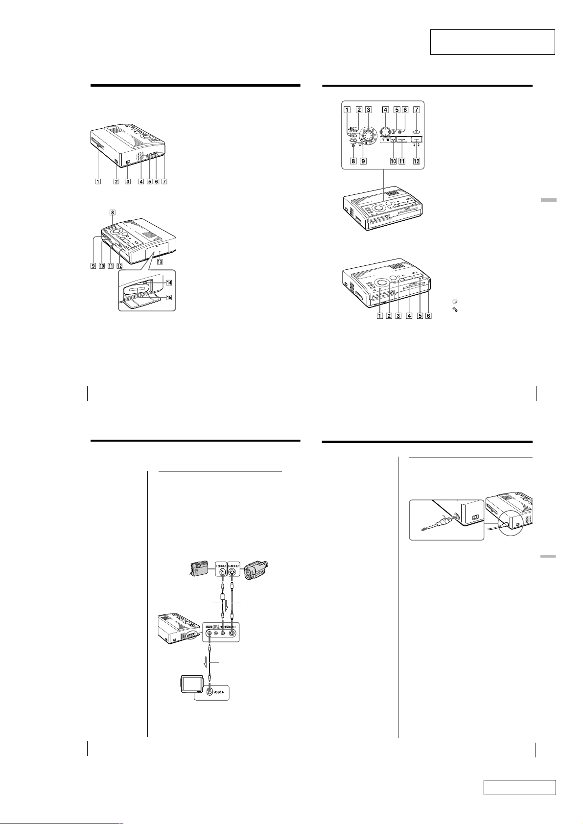
Identifying the partsIdentifying the parts
See the pages given in parentheses for use of the parts.
1 Paper outlet (page 47)
2 AC power connector (page 9)
3 POWER switch (page 10)
4 VIDEO OUTPUT connector (page 8,
19)
5 REMOTE CAPTURE jack (page 39)
6 VIDEO INPUT connector (page 8)
7 S VIDEO INPUT connector (page 8)
8 Operation panel (page 7)
9 3.5-inch floppy disk insertion slot
(page 19)
0 3.5-inch floppy disk eject button
(page 19)
qa Cover for the automatic feeder
(page 17)
qs Paper inlet/outlet for manual
feeding (page 17, 47)
qd Cartridge door (page 13, 14)
qf Eject lever (page 14)
qg Print cartridge (page 13, 14) (not
supplied)
Cartridge compartment
Operation Panel
1 MIRROR IMAGE SELECT switch
(page 30)
2 INPUT SELECT switch (page 20, 23)
3 Print mode dial (page 21, 24, 26, 28,
32, 34)
4 Arrow buttons (B/b/V/v) (page
24)
5 ENTER button (page 24)
6 CLEAR ALL button (page 21)
7 SAVE button (page 36)
8 CLOCK SET button (page 10)
9 DATE switch (page 38)
0 PICTURE button (page 23, 25)
qa CAPTURE button (page 21, 24)
qs PRINT button (page 22, 25)
Indicators
1 POWER indicator (page 10)
2 INPUT indicator (page 21, 45)
3 MEMORY indicator (page 21, 45)
4 Print indicator (page 22, 25, 45)
5
Paper supply indicator (page 45)
6
Ribbon error indicator (page 45)
Getting
Started
GB
Getting Started
6
Setting Up
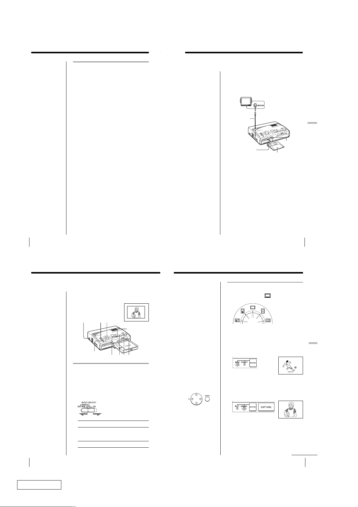
Connecting the printer
Connecting to the video equipment
When printing images from the video equipment such
as a VCR or camcorder, use the supplied video
connecting cable to connect the video equipment and
the printer. Also connect the printer to the television to
display the images to be printed.
For printing operations, see page 20.
If the video equipment
has the S-video output
connector
Connect it to the S VIDEO
INPUT connector of the
printer using the optional
S-video connecting cable
so that you can get better
picture quality. In this
case, you do not need to
connect the video
connector.
When both the S VIDEO
INPUT and VIDEO INPUT
connectors of the
printer are connected
The input signals from
the S VIDEO INPUT
connector are
automatically selected.
Notes
• Before making
connections, turn off
the power of the
printer, the video
equipment and
television.
• See also to the
instruction manuals for
the video equipment.
GB
Setting Up
8
Digital still camera or
video camera
equipped with the
video output
connector
Video connecting
cable (not supplied)
To VIDEO
INPUT
Television
Set input selector to
“VIDEO.”
Video camera or
Or
etc. equipped with
the S-video output
connector
S-video connecting
cable (not
supplied)
To S VIDEO
INPUT
To VIDEO OUTPUT
Video connecting
cable (supplied)
l
: Signal flow
Getting Started
Connecting the AC power cord
After you make connections, connect the supplied AC
power cord to the AC power connector of the printer
and then to the AC outlet.
AC Power cord
(supplied)
To the AC outlet
Setting Up
GB
7
Setting Up
GB
9
1-1
Confidential
DMP-1000P (AEP)
Page 4

Adjusting the clock
You can save the time when the images are captured
from the video equipment by adjusting the clock of the
printer. Once you adjust the clock, the clock is
maintained with the battery even if you turn off the
power.
1
Turn on the power of the printer.
The POWER indicator lights up.
4
Press b.
The cursor moves to the next item.
5
Repeat steps 3 and 4 to set all items: month, date,
year, hour and minute.
If you want to set the previous item, press B.
POWER switch
2
Press and hold CLOCK SET, then press b.
The clock setting display appears on the television.
3
Press V/v to set the month.
Pressing V increases the number.
Pressing v decreases the number.
GB
Setting Up
10
Using optional supplies
(print packs)
You need an optional print pack. The pack contains
print paper and ink ribbon cartridge for printing.
The following types of print packs are available:
Print Model Print paper Print cartridge
Standard DPM-50STA Standard type for 50 prints
POWER indicator
6
Press CLOCK SET.
The clock setting display disappears.
Displaying the clock
When the INPUT indicator is on, press CLOCK SET to
display the current time on the center of the screen. To
turn off the time display, press CLOCK SET again.
Loading the print cartridge
Insert the print cartridge into the printer.
Use only the print cartridge supplied with the print
paper packed in the same carton.
Caution
Never put your hand into
the cartridge
compartment. The
thermal head reaches
high temperatures,
especially after repeated
printing.
1
Press PUSH to open the cartridge compartment lid.
Setting Up
Setting Up
GB
11
Note
Use the set of the print
paper and ink ribbon
cartridge supplied
together in the same
carton. If you use them in
different combination,
proper printing results
may not be obtained, or
paper jam or other trouble
may occur.
GB
Setting Up
12
Confidential
DMP-1000P (AEP)
1-2
Notes
• If the print cartridge is
not loaded when you
turn on the printer, the
warning sound beeps
and the ribbon error
indicator lights up.
• When installing the ink
ribbon cartridge, stand
it as illustrated so that
dust will not get on the
ink ribbon.
• Do not touch the ink
ribbon or place the
print cartridge in a
dusty location.
Fingerprints or dust on
the ink ribbon may
result in imperfect
printing.
2
Wind up the ink ribbon to remove the slack.
While pressing the
center of the reel, wind
the ink ribbon in the
direction of the arrow.
Wind the ribbon
until the black
line comes to the
left edge.
3
Insert the print cartridge firmly until it clicks into
place and close the cartridge compartment lid.
If the print cartridge does not click into place
Remove the print cartridge, and then re-insert it.
Labeled side
continued
Setting Up
Setting Up
GB
13
Page 5

Loading the print cartridge (continued)
To replace the print cartridge
If the ribbon indicator flashes and the inserted paper
emerges after you insert the paper and the paper is
automatically loaded, remove the print paper and
replace the print cartridge.
Open the cartridge compartment lid and push up the
eject lever. Remove the used print cartridge and
replace it with a new one.
To load the half-used ink ribbon cartridge
Wind the ribbon
until the black
line comes to the
left edge.
Notes on storing the
print cartridge
• Avoid placing the
cartridge in a location
subject to:
– high temperatures
– high humidity
– excessive dust
– direct sunlight
• When you are going to
store a partially-used
cartridge for an
extended period of
time, store it in its
original bag.
GB
Setting Up
14
If ink ribbon should tear
Repair the ribbon with transparent tape. There should
be no problem with using the remaining portion of the
ribbon. Before loading the ink ribbon cartridge into the
printer, turn the reel until the transparent tape can no
longer be seen.
Eject lever
Paper supply indicator
Ribbon error indicator
Push up the eject lever,
then remove the used
print cartridge.
While pressing the
center of the reel, wind
the ink ribbon in the
direction of the arrow.
Repair with
transparent tape.
Inserting the print paper
Inserting the print paper using the
supplied automatic feeder
By using the supplied automatic feeder, you can
supply the print paper automatically.
1
Open the lid of the paper tray by sliding the switch
on front to the right.
Notes on using
automatic feeder
• If trouble occurs in
feeding the print paper,
the lamp on the printer
flashes. Remove the
feeder from the printer
and check that there is
no paper jammed in the
printer. When you
reinstall the feeder and
press the print button,
the printer prints the
set number of copies
again.
• The feeder can hold up
to 25 sheets of paper.
When you add paper to
a partially full feeder,
make sure that the total
number of sheets does
not exceed this limit. If
you do, the paper may
jam.
• Do not place different
types of paper in the
feeder. If you do, the
paper may jam.
• To insert paper after
the feeder is attached to
the printer, first remove
the feeder from the
printer and then insert
the paper into the
feeder.
• While printing, do not
open the feeder lid. If
you do, the paper may
jam.
2
Make sure that the spacer is raised.
Spacer
3
Riffle the print paper to avoid jamming the print
paper.
Make sure not to touch the printing surface (the
glossy side where nothing is printed).
Setting Up
Setting Up
GB
15
Inserting the print paper (continued)
To print a number of
copies not specified on
the dial
Insert the desired number
of sheets and set the dial
to 25.
GB
Setting Up
16
4
Insert print paper with its printing surface (the side
where nothing is printed) facing up.
Make sure not to touch the printing surface and not
to bend the corners of the paper. You can load up
to 25 sheets of print paper or the print paper
designed for the printer into the feeder.
Make sure that the metal tabs on both sides fir over
the print paper.
Printing surface
Front
Paper
Metal tab
5
Turn on the printer and press MEMORY or
CAPTURE to store an image for printing.
For the details, refer to “Printing” in the operating
instructions of the printer.
6
Turn the dial to set the number of copies to be
printed continuously.
You can set 1, 2, 3, 4, 5,10 or 25 copies. Turn the
dial until the desired number appears in the
window. Make sure it clicks at that time.
Otherwise, you may get the wrong number of
copies.
2
To stop continuous
printing
Set the dial to 1. Printing
stops after the current
printing finishes.
If print paper runs out
during continuous
printing
Remove the feeder from
the printer. Then, insert
more print paper into the
feeder and reinstall the
feeder to the printer. The
printing resumes
automatically.
Notes on inserting the
print paper manually
• Insert the print paper
straight along the guide
to the left of the paper
port. If the paper is
positioned to the right
or slanted, the printing
area may get out of
position.
• The paper may not be
loaded automatically if
you do not insert the
paper firmly.
7
Press “Push” on the cover of the automatic feeder,
then insert the feeder until it clicks.
8
Press the print button of the printer.
The print paper is automatically loaded into the
printer and printing starts.
Inserting the print paper manually
Insert the print paper sheet by sheet. This section
explains how to insert the standard type print paper.
Use the print paper designated for this printer only.
1
Turn on the power of the printer.
The POWER indicator lights up.
2
Follow printing procedures.
For details, see pages 20 to 39.
3
Insert the print paper straight with its blank
printing surface facing up, along the guide to the
left of the paper port.
Insert the paper until less than 2 cm (approx. 0.8
inches) remains. The paper is automatically loaded
when printing starts.
Guide
Less than 2 cm
Setting Up
Setting Up
GB
17
1-3
Confidential
DMP-1000P (AEP)
Page 6
Inserting the print paper (continued)
GB
Setting Up
18
Notes on handling the print paper
• You cannot type on the printing surface before
printing. If you want to write greetings or draw on
the printing surface after printing, use an oil ink pen.
• When handling the print paper, do not touch the
printing surface (glossy side where nothing is
printed).
• Do not place the print paper in a dusty location.
Fingerprints or dust on the printing surface may
result in imperfect printing.
• Use the print paper designed for the printer only. If
you use a different type of paper, the printer may not
print properly or may malfunction.
• Do not fold or bend the print paper.
Notes on storing the print paper
• Avoid placing the print paper in a location subject to:
– high temperatures
– high humidity
– excessive dust
– direct sunlight
• When you are going to store the partially-used print
paper for an extended period of time, store it in its
original bag.
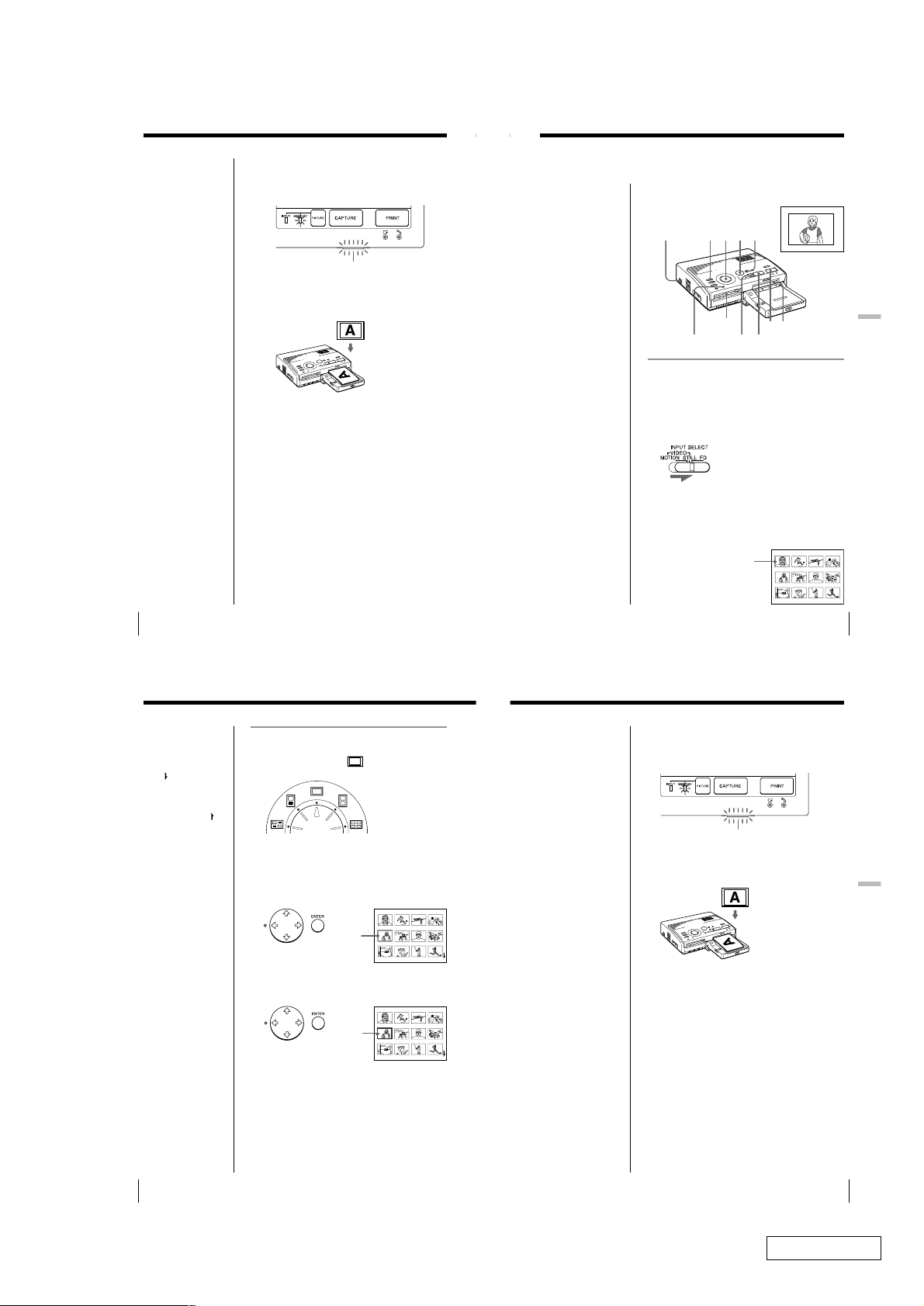
Using the floppy disk
When printing images recorded on the floppy disk,
insert the floppy disk into the insertion slot for the 3.5inch floppy disk of the printer. Also connect the printer
to the television to display the images to be printed.
For printing operations, see page 23.
Video connecting
cable (supplied)
To VIDEO
OUTPUT
With the arrow facing
left forward and insert
the disk firmly, facing
down.
Ejecting the floppy disk
Press the floppy disk eject button.
Usable floppy disks
You can use a 3.5-inch 2HD 1.44MB floppy disk in the
Notes
• Before making
connections, turn off
the power of both the
printer and television.
• If the floppy disk does
not fit properly, do not
attempt to force it into
the slot. Confirm the
inserting direction
again and re-insert it
into the slot.
MS-DOS format.
Television
Set input selector
to “VIDEO.”
Floppy disk
Floppy disk
eject button
Setting Up
Setting Up
GB
19
Printing
Printing an image from the video
equipment
You can capture the input image from the video
equipment connected to the VIDEO INPUT connector
of the printer and print it in full-size (standard print).
Preparation1Preparation
POWER indicator
Preparations
1
Turn on the printer and television and set the input
selector of the television to “VIDEO.”
The POWER indicator turns on.
2
Set INPUT SELECT to “VIDEO MOTION” or
“VIDEO STILL.”
To Selector position
Print the motion picture VIDEO MOTION
while compensating for the
image blur
Print the still image VIDEO STILL
GB
Printing
20
2
PICTURE
1
Standard print
CLEAR ALL
34 5
Blur compensation
When you set INPUT
SELECT to “VIDEO
MOTION,” the selected
image appears on the
screen and the horizontal
red line moves from the
top to the bottom on the
left half of screen, then
moves from the top to the
bottom on the right half of
screen. In this sequence, if
there is motion blur on
the image, the printer
automatically
compensates for the
image (blur
compensation).
When the blur
compensation ends, the
screen darkens once and
the print image appears in
the screen.
Re-selecting the image
Press B before pressing
PRINT. The playback
picture appears on the
screen.
You can also re-select the
image by pressing
PICTURE instead of
pressing B. (You cannot
capture a image while the
MEMORY indicator lights
up. Press CAPTURE
while the MEMORY
indicator goes off.)
If you press CLEAR ALL,
the printer is reset to
stand by mode.
Perform printing
procedures from the
beginning.
Printing
1
Set print mode dial to “ (standard)”.
2
Start playback on the video equipment.
While the INPUT indicator lights up, the playback
picture appears on the screen (input picture).
For details on playing back on the video
equipment, refer to the instruction manual of your
equipment.
Input image
3
Press CAPTURE when the picture you want to
print appears on the screen.
The selected full-size image appears in the screen,
and the MEMORY indicator lights up.
Print image
continued
Printing
Printing
GB
21
Confidential
DMP-1000P (AEP)
1-4
Page 7
Printing an image from the video equipment (continued)
4
Press PRINT.
The print indicator flashes and the print paper
is automatically loaded. The paper supply
indicator flashes while loading the print paper.
Printing an image recorded on the
floppy disk
You can select an image recorded on the floppy disk
and print it in full-size (standard print).
Notes
• While printing, never
move or turn off the
printer; the print
cartridge or paper may
become stuck. If this
happens, turn the
printer off and on, and
resume printing from
the beginning.
• Do not insert another
sheet of print paper
until you remove the
printed sheet.
• During printing, the
print paper is partially
ejected from the paper
outlet several times.
Never pull out the
paper forcibly.
• It is not recommended
to select an image while
pausing the video
equipment because the
picture quality will be
lost.
• Avoid storing the paper
with the printed faces
contacting each other or
contacting with rubber
or plastic products
including vinyl
chloride or plasticizer
for an extended period
of time; the ink may
transfer on to them.
If the print paper is not
loaded
The print indicator and
the paper supply
indicator flash.
Insert the print paper.
GB
Printing
22
Print indicator
Printing direction
The image displayed on the digital camera is
printed in the direction as shown below.
Displayed image
Printed image
5
Remove the print from the printer.
When printing ends, the print paper
automatically emerges from the print outlet.
The print indicator turns out.
Printing the same image again
Make sure that the desired image is displayed on
the screen, then press PRINT.
With the supplied automatic feeder, you can print
the same image continuously up to 25 sheets.
Capturing a picture by using the optional foot
switch
You can use the optional foot switch FS-20 to select
the disired image instead of using CAPTURE.
For details, see “Capturing a picture by using the
optional foot switch” on page 39.
Notes
• Avoid getting liquids
on the floppy disk or
using floppy disks in
areas subject to high
humidity. Otherwise,
data may be rendered
unreadable.
• When the access
indicator is lit, do not
eject the floppy disk.
Otherwise, the disk
may crash.
Preparation1Preparation
POWER indicator PICTURE
2
Preparation
123
3
45
CAPTURE
Standard print
Preparations
1
Turn on the printer and television and set the input
selector of the television to “VIDEO.”
The POWER indicator lights up.
2
Set INPUT SELECT to “FD.”
3
Insert the floppy disk on which you record images
into the floppy disk insertion slot. (page 19)
While the printer is accessing the floppy disk, the
access indicator flashes. When the printer ends
reading images, recorded images are displayed as
thumbnails.
White
frame
(cursor)
Printing
Printing
GB
23
Printing an image recorded on the floppy disk (continued)
Scrolling the pages
When multiple pages
exist, you can change the
pages back and forth. To
display the next page
(when
bottom-right), move the
white frame to the bottom
line of the image list and
press v. To display to the
previous page (when
appears at the top-right),
move the white frame to
the top line and press V.
The access lamp flashes
and pages switches.
Cancelling the selection
Move the white frame to
the image you want to
cancel the selection and
press ENTER. The blue
frame disappears and the
selection is canceled.
Selecting multiple
images
Repeat steps 2 and 3 until
you select all images you
want to print.
Displaying the image in
full-size
Move the white frame to
the desired image, then
press CAPTURE in step 3.
The selected full-size
image appears in the
center of the screen.
To display the next or
previous full-size image,
press v (next image) or V
(previous image).
If you want to re-select
the image, press
PICTURE to return to the
image list then repeat
steps 2 and 3.
Note
The displayed full-size
image may not
correspond with the
actual print in details.
GB
Printing
24
appears at the
Printing
1
Set print mode dial to “ (standard)”.
2
Press the arrow (B/b/V/v) buttons to move the
white frame (cursor) to the image you want to
print.
Move the white frame up (V), down (v), rightward
(b) , or leftward (B).
Move the
white frame.
3
Press ENTER.
The blue frame appears inside the white frame and
the selected image is specified to be printed.
The white
frame
changes to
blue.
Notes
• An image which is
damaged or has some
trouble does not appear
in the image list.
• If there are no images
stored in the floppy
disk, “NO FILE”
appears on the display.
• If you press PRINT
while displaying the
actual print image, only
the displayed image is
printed.
• If you press PRINT
while displaying the
thumbnail list, all
images with the blue
frame are printed.
• While printing, never
move or turn off the
printer; the print
cartridge or paper may
become stuck. If this
happens, turn the
printer off and on, and
resume printing from
the beginning.
• Do not insert another
sheet of print paper
until you remove the
printed sheet.
• During printing, the
print paper is partially
ejected from the paper
outlet several times.
Never pull out the
paper forcibly.
• Avoid storing the paper
with the printed faces
contacting each other or
contacting with rubber
or plastic products
including vinyl
chloride or plasticizer
for an extended period
of time; the ink may
transfer on to them.
If the print paper is not
loaded
The print indicator and
the paper supply
indicator flash.
Insert the print paper.
4
Press PRINT.
The print indicator flashes and the print paper is
automatically loaded. The paper supply indicator
flashes while loading the print paper.
Print indicator
Printing direction
The image displayed on the digital camera is
printed in the direction as shown below.
Displayed image
Printed image
5
Remove the print from the printer.
When printing ends, the print paper automatically
emerges from the print outlet.
The print indicator turns out.
Printing the same image again
Press PRINT.
With the supplied automatic feeder, you can print the
same image continuously up to 25 sheets.
Printing other images
Press PICTURE so that the thumbnail screen appears,
then perform steps 1 to 5.
Printing multiple images continuously
You can print multiple images continuously up to 25
sheets using the supplied automatic feeder.
Printing
Printing
GB
25
1-5
Confidential
DMP-1000P (AEP)
Page 8

Making Various Print
Making split prints
GB
Making Various Prints
26
Printing images from the video
equipment
You can make prints divided into multiples of 1/2-, 1/
4- or 1/16-size pictures. You can also select the same
image, or different images for the split print.
Before you begin
1 Turn on the printer and television and set the input
selector of the television to “VIDEO.”
2 Set INPUT SELECT to “VIDEO MOTION” or
“VIDEO STILL.”
1
Select the type of split using the print mode dial.
You can select 2-split, 4-split, 16-split planes of the
same image or different images.
2-split printing using
different images
4-split printing
using different
images
16-split printing using
different images
2-split printing using
the same image
4-split printing
using the same
image
16-split printing using
the same image
When you select “VIDEO
MOTION”
When you set INPUT
SELECT to “VIDEO
MOTION,” the selected
image is blurcompensated in step 2.
Re-selecting the image
Press CLEAR ALL. The
selected image is removed
and the printer returns to
stand by mode.
Perform printing
procedures from the
beginning.
You can also re-select the
image by pressing B.
When you set to split
printing with the different
images and re-select the
image by pressing B, only
a image that you most
recently selected is
removed.
When you set to split
printing with the same
images, you can also
press PICTURE to display
the input picture, then reselect a new image. (You
cannot capture a image
while the MEMORY
indicator lights up. Press
CAPTURE while the
MEMORY indicator goes
off.)
2
Select the image.
• When selecting the same image for all the split
planes:
1 Turn on the video
equipment and start
playback.
2 Press CAPTURE when the
picture you want to print
appears on the screen.
The memory image is
displayed in the split
planes selected in the step
1.
• When selecting the different images for each split
plane:
1 Turn on the video equipment and start
playback.
2 Press CAPTURE when the picture you want to
print appears on the screen.
The memory image is displayed in the first
plane of the split planes selected in the step 1.
After a while, the memory image disappears
and the input picture automatically appears.
3 Repeat step 2 until you select images for all
split planes.
When you select 4split printing
The selected pictures are allocated as follows:
upper left t upper right t lower left t
lower right.
When you select 4-split printing
3
Press PRINT.
The print indicator flashes while printing, and the
selected image is printed.
Making Various Prints
Making Various Prints
GB
27
Making split prints (continued)
Printing the date
You can print the date
when the image was
saved by setting DATE to
“ON.”
GB
Making Various Prints
28
Printing images from the floppy disk
You can make prints divided into multiples of 1/2-, 1/
4- or 1/16-size pictures. You can select the same image,
or different images for the split print.
Before you begin
1 Turn on the printer and television and set the input
selector of the television to “VIDEO.”
2 Set INPUT SELECT to “FD.”
3 Insert the floppy disk into the floppy disk slot.
1
Select the type of split using the print mode dial.
You can select 2-split, 4-split, 16-split planes of the
same image or different images.
2-split printing using
different images
4-split printing
using different
images
16-split printing using
different images
2
Select the image.
• When selecting the same image for all the split
planes:
1 Press arrow button to move the white frame to
the image you want to print, then press
ENTER. (The blue frame appears inside the
white frame.)
2 If you want to make other same image prints,
repeat step 1.
2-split printing using
the same image
4-split printing
using the same
image
16-split printing using
the same image
Re-selecting the image
Move the white frame to
the image you want to
cancel the selection for
and press ENTER. The
blue frame disappears
and the selection is
canceled.
If you want to re-select
the image after displaying
the actual print image,
press PICTURE to return
to the thumbnail screen,
then repeat step 2.
Re-selecting the type of
the split
Press PICTURE so that
the thumbnail screen
appears. Re-select the
split type using the print
mode dial. You can use
the selected images, or
change the selection.
Canceling the operation
Press CLEAR ALL. The
selected image is removed
and the printer returns to
stand by mode.
Perform printing
procedures from the
beginning.
Note
If you press PRINT when
the actual print image is
displayed, only the
displayed image is
printed.
• When selecting the different images for each split
plane:
1 Press the arrow button to move the white
frame to the image you want to print, then
press ENTER. (The blue frame appears inside
the white frame.)
2 Repeat step 1 to select images for the split
planes in the desired order.
The pictures are placed
from the upper left to the
lower right on the sheet in
order of the selection, not
in order of the image list.
You can also select an image from the different
pages.
If you select more images than the number of
the split planes, the images are automatically
placed on the next print.
To check the actual print image
Press CAPTURE.
The actual print image appears in the center of the
screen.
To display multiple split prints, press V or v.
When you select 4split printing using a
same image
3
Press PRINT.
The print indicator flashes while printing, and the
selected image is printed.
When you select 4split printing using
different images
Making Various Prints
Making Various Prints
GB
29
Confidential
DMP-1000P (AEP)
1-6
Page 9

Making a mirror image print
You can make a mirror image or upside-down mirror
image when you print a picture from video equipment.
You can use this feature with the standard printing
(page 20 to 22) and split printing (page 26 to 27).
Before you begin
1 Turn on the printer and television and set the input
selector of the television to “VIDEO.”
2 Set INPUT SELECT to “VIDEO MOTION” or
“VIDEO STILL.”
1
Set MIRROR IMAGE SELECT to the desired type of
image reversal.
Vertically reversed
(upside-down image)
No reversal
(original image)
2
Start playback on the video equipment.
While the INPUT indicator lights up, the playback
picture appears on the screen (input picture).
3
Press CAPTURE when the picture you want to
print appears on the screen.
The selected picture appears. When you set
MIRROR IMAGE SELECT to “V” or “H,” “R”
(reversed) mark appears on the lower right of the
screen.
Note
You cannot make a mirror
image print when you
want to print the image in
the floppy disk.
GB
Making Various Prints
30
Horizontally
reversed
(mirror image)
: Indicates an upside-down
mirror image.
: Indicates a mirror image.
4
Press PRINT.
The mirror image is printed.
Making a mirror image print in the split
printing mode
Set MIRROR IMAGE SELECT to the desired type
before performing the printing procedures in the
“Printing images from the video equipment” (page 26).
When you use different images
You can change the mirror image type for each split
plane.
Example
• Plane 1 and 3: vertically reversed
• Plane 2 and 4: horizontally reversed
Vertically
reversed
Horizontally
reversed
To change the mirror image type for each split plane,
change the MIRROR IMAGE SELECT setting each time
before you press CAPTURE.
When you use the same image
The same mirror image in the split planes is printed.
Making Various Prints
Making Various Prints
GB
31
Making a label for a floppy disk
You can make a label for a floppy disk by using the
sticker-type print paper.
The selected image is printed as large picture on one
label, and 3 thumbnail images with lines are printed on
the other label. The total number of images is printed
at the bottom left of the label.
Before you begin
1 Turn on the printer and television and set the input
selector of the television to “VIDEO.”
2 Set INPUT SELECT to “FD.”
1
Select “ (FD label print)” using the print mode
dial.
FD label print
2
Select the image for printing.
1 Insert the floppy disk into the floppy disk slot.
2 Press the arrow buttons to move the white
frame to the image you want to print, then
press ENTER.
When printing the input
image from the video
equipment
You cannot make a label
for a floppy disk.
Printing the date
You can print the date
when the image was
saved by setting DATE to
“ON.”
GB
Making Various Prints
32
The selected image is placed on the upper half
of the print and the leftmost of the thumbnail
on the lower half.
Cancelling the selection
Move the white frame to
the image you want to
cancel the selection and
press ENTER. The blue
frame disappears and the
selection is canceled.
To remove the all selected
images, press CLEAR
ALL.
Perform printing
procedures from the
beginning.
Note
You cannot type on the
printing surface before
printing. If you want to
write greetings or draw
on the printing surface
after printing, use an oil
ink pen.
3 Repeat step 2 to select images for the other 2
thumbnails.
4 Press CAPTURE if you want to check the
actual print image.
To display multiple print images, press V or v.
The first
selected image
The second and
third selected
images
Total images
Date (when set
to print)
3
Insert the sticker type paper into the printer, then
press PRINT.
The print indicator flashes while printing, and the
label for the floppy disk is printed.
You can use each part of the label for the floppy
disk. Cut the paper so it fits the label side.
Making Various Prints
Making Various Prints
GB
33
1-7
Confidential
DMP-1000P (AEP)
Page 10
Making an index list of images
You can make an index list of images saved in a floppy
disk. When you want to search for the recorded image,
you can find the desired images immediately with this
index list.
Before you begin
1 Turn on the printer and television and set the input
selector of the television to “VIDEO.”
2 Set INPUT SELECT to “FD.”
1
Select “ (Index print)” using the print mode
dial.
Index print
2
Insert the floppy disk into the floppy disk slot.
All the images recorded in the floppy disk are
displayed in a thumbnail list.
If there are multiple pages, press V or v to display
the next or previous page.
About date printing
The date when the image
was saved is printed
regardless of the DATE
setting. However, the date
does not appear on the
displayed image.
GB
Making Various Prints
34
Notes
• If the number of images
is less than that of split
planes, planes without
images remain blank.
• If the number of image
is over 43, the image
number 43 or more is
not printed.
To display the actual print image
Press CAPTURE.
All the images recorded in the floppy disk are
displayed as the thumbnail images.
3
Press PRINT.
The print indicator flashes while printing, and the
index list of the recorded images on the floppy disk
is printed.
The size of each image depends on the number of
the images.
• When the number of images is 1 to 12
The images are made into the
size of 12 thumbnails. Each
thumbnail has the
corresponding image
number.
• When the number of images is 13 to 20
The images are made into the
size of 20 thumbnails. Each
thumbnail has the
corresponding image
number.
• When the number of images is over 21
The images are made into the
size of 42 thumbnails. Each
thumbnail has the
corresponding image
number.
Making Various Prints
Making Various Prints
GB
35
Recording the video picture as
a still image
You can record the playback picture from the video
equipment as a still image onto the floppy disk.
Before you begin
1 Turn on the printer and television and set the input
selector of the television to “VIDEO.”
2 Set INPUT SELECT to “VIDEO MOTION” or
“VIDEO STILL.”
1
Set the print mode dial to “ (standard)” or split
When you set the print
mode dial to the split
mode
You can also record the
picture in the split mode.
In this case, only the most
recently selected picture
is recorded onto the
floppy disk.
Re-selecting the image
Press PICTURE before
pressing SAVE. The
playback picture appears
on the screen. Follow step
2. (You cannot capture a
image while the
MEMORY indicator lights
up. Press CAPTURE
while the MEMORY
indicator goes off.)
You can also re-select the
image by pressing the
arrow (B) instead of
pressing PICTURE.
If you press CLEAR ALL,
the printer is reset to
stand by mode.
Perform printing
procedures from the
beginning.
GB
Making Various Prints
36
printing mode.
2
Select the image to be recorded.
For details of operating procedures, refer to the
pages for the corresponding printing mode.
1 Turn on and start playback on the video
equipment.
2 Press CAPTURE when the picture you want to
record appears on the screen.
3
Insert the floppy disk into the floppy disk slot.
Insert a floppy disk formatted in the MS-DOS
format. Check that the write protect switch on the
disk is set to the write enable position.
4
Press SAVE.
The access indicator of the floppy disk drive lights
up, and the displayed image is recorded onto the
floppy disk.
About file name of the recorded image
The image is recorded with the file name “MVC-###f
.jpg.” The number “###” is sequentially allocated
following the largest file number (same as the image
number) recorded in the floppy disk.
If an error message appears
Error message Meaning
DISK ERROR The inserted floppy disk is not
DISK FULL There is not enough space to
DISK PROTECT The write protect tab on the
formatted.
Insert a disk in the MS-DOS
format.
record the image.
Replace the floppy disk with new
one.
inserted floppy disk is set to write
protect position. Set it to the write
enable position and then record
the image.
Making Various Prints
Making Various Prints
GB
37
Confidential
DMP-1000P (AEP)
1-8
Page 11
Printing the date
39
GB
Making Various Prints
Making Various Prints
Capturing the picture using
the optional foot switch
When you make a print from the video equipment, you
can use the optional foot switch FS-20 to select the
desired image remotely.
Connecting the optional foot switch
Connect the optional foot switch FS-20 to REMOTE
CAPTURE jack on this unit.
Using the optional foot switch
When you select the desired picture, use the optional
foot switch instead of pressing CAPTURE.
Notes
• Turn off the power of
this unit before
connecting the optional
foot switch.
• You cannot use other
remote controller for
this unit.
Optional foot
switch FS-20
To REMOTE
CAPTURE
GB
Making Various Prints
38
When printing the image in the
floppy disk, you can print the
date shot with the Digital
Mavica.
Note that you cannot print the
date when you print the image
from the video equipment.
Before you begin
1 Turn on the printer and television and set the
input selector of the television to “VIDEO.”
2 Set INPUT SELECT to “FD.”
1
Set DATE to “ON.”
Date is not printed.
Date is printed.
2
Select the desired print using the print mode
dial.
You can select standard printing (page 20, 23),
split printing (page 26 to 29), label printing
(page 32) or index printing (page 34).
3
Select the image for printing.
1 Insert the floppy disk into the floppy disk
slot.
2 Press the arrow buttons to move the white
frame to the image you want to print, then
press ENTER.
4
Press PRINT.
The selected image is printed with the date.
Date
For Your Information
Precautions
On safety
• Operate the printer on 220 to 240 V AC, 50/60 Hz
only.
• Be careful not to set or drop any heavy objects on the
power cord, or to damage the power cord in any
way. Never operate this printer with a damaged
power cord.
• Should any solid object or liquid fall into the cabinet,
unplug the printer and have it checked by qualified
personnel before operating it any further.
• Never disassemble the printer.
• To disconnect the power cord, pull it out by the plug.
Never pull the power cord itself.
• When the printer is not going to be used for an
extended period of time, disconnect the power cord
from the wall outlet.
• Do not handle the printer roughly.
• To reduce the risk of electrical shock, always unplug
the printer from electrical outlet before cleaning and
servicing the printer.
On installation
• Avoid placing the unit in a location subject to:
– vibration
– high humidity
– excessive dust
– direct sunlight
– extremely high or low temperatures
• Do not use electrical equipment near the unit. The
unit will not work properly in electromagnetic fields.
• The unit is designed to operate horizontally. Never
attempt to operate the printer in a tilted position. If
the unit was placed on its side or with its top panel
facing down, make sure to remove the paper tray
and check that the print papers are set properly
before starting operation.
• Do not place heavy objects on the printer.
• Leave enough room around the printer so that the
ventilation holes are not blocked. Blocking these
holes may cause internal heat build-up.
On moisture condensation
If the printer is brought directly from a cold location to
warm location or placed in an extremely warm or
humid room, moisture may condense inside the unit.
In such cases the printer will probably not work
properly and may even develop a fault if you persist in
using it. If moisture condensation occurs, turn off the
power and do not use the printer for at least one hour.
On transport
When you transport the printer, remove the print
cartridge from the printer and put the unit in the
original box with the protective packaging.
If you no longer have the original box and packing
parts, use the substitutive packing material so that it
will not be damaged while transporting.
On cleaning
Clean the cabinet, panel and controls with a soft dry
cloth, or a soft cloth lightly moistened with a mild
detergent solution. Do not use any type of solvent,
such as alcohol or benzine, which may damage the
finish.
For Your Information
GB
For Your Information
40
For Your Information
GB
41
Confidential
1-9
DMP-1000P (AEP)
Page 12

Precautions (continued)
On floppy disks
To protect data recorded on floppy disk, note the
following:
• Avoid storing floppy disks near magnets or magnetic
fields such as those of speakers and televisions,
permanent erasure of disk data may result.
• Avoid storing floppy disks in areas subject to direct
sunlight or sources of high temperature, such a
heating device. Floppy disk warping of damage may
result, rendering the disk useless.
• Avoid contact with the disk’s surface by opening the
disk shutter plate. If the disk’s surface becomes
blemished, data may be rendered unreadable.
• Avoid getting liquids on the floppy disk or using
floppy disks in areas subject to high humidity.
Otherwise, data may be rendered unreadable.
• Be sure to use the floppy disk case to ensure
protection of important data.
• Use only a 2HD type disk head cleaner when
cleaning the disk drive.
• Even when you use a 3.5 inch 2HD floppy disk,
image data may not be recorded and/or displayed
depending on the using environment. In this case,
use the other brand disks.
Back up recommendation
To avoid the potential risk of data loss, always copy
(back up) data to the other floppy disk.
On print paper
Use the set of the print paper and print cartridge
supplied together in the same carton. If you use them
in different combination, proper printing results may
not be obtained, or paper jam or other trouble may
occur.
Chart for various print mode
Split printing using the same image (page 26, 28)
Standard printing
(page 20, 23)
Date printing
(page 38)
Mirror printing
(page 30)
2-split printing
Split printing using different images (page 26, 28)
2-split printing
Floppy disk
label printing
(page 32)
4-split printing 16-split printing
4-split printing
Index printing (page 34)
16-split printing
GB
For Your Information
42
GB
For Your Information
50
Confidential
DMP-1000P (AEP)
1-10
1-10 E
Page 13

SECTION 2
)
DISASSEMBLY
Note: Follow the disassembly procedure in the numerical order given.
UPPER CABINET ASSY
2 upper cabinet Assy
3 flat cable (DKSW39
(CN504)
1 two screws
(BVTP3 × 20)
DC FAN (HEAD FAN) (M901)
1 connector
(CN1938)
2 two screws
(BTP2.6 × 12)
1 two screws
(BVTP3 × 20)
4 cushion, fan
3 DC fan (head fan) (M901)
2-1
Confidential
DMP-1000P (AEP)
Page 14
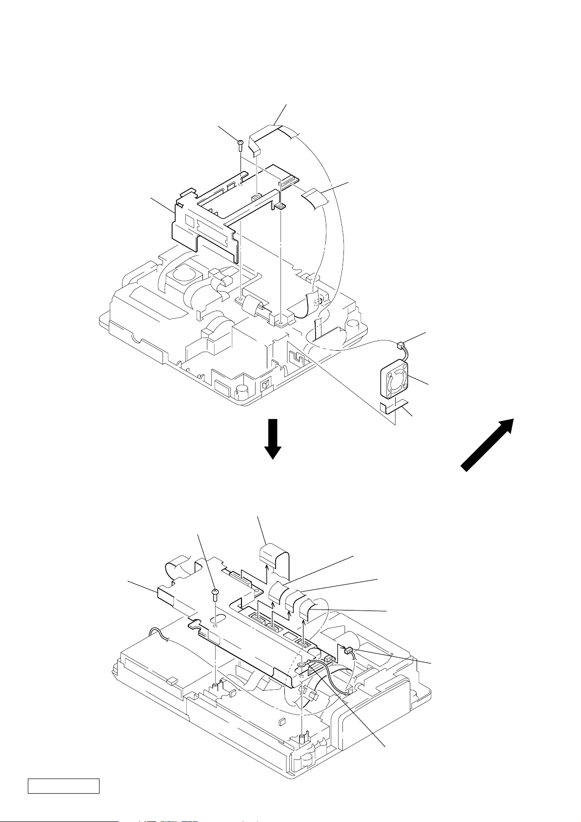
VI-39 BOARD SECTION, DC FAN (POWER FAN) (M905)
)
k
4 flat cable (VIVS39)
(CN101)
5 two screws
(BV2.6 × 8)
6 VI-39 board section
4 flat cable (VIDK20)
(CN102)
1 connector
(CN402)
DK-39E BOARD SECTION
5 DK-39E board section
2 DC fan (power fan
(M905)
3 cushion
(9 × 50 × 0.2)
1 flat cable (DKFD39)
(CN2100)
3 two screws
(BV2.6 × 8)
1 FP-700 flexible board
(CN501)
1 flat cable (ADFE13)
(CN503)
1 flat cable (ADHE13)
(CN502)
2 mini jack bloc
Confidential
DMP-1000P (AEP)
4 harness
2-2
Page 15

FLOPPY DISK DRIVE (3.5 inch)
s
5 floppy disk drive (3.5 inch)
2 two screws
(BV2.6 × 8)
4 screw
(M2 × 3)
1 flat cable (DKFD39)
3 FD bracket Assy
4 two screw
(M2 × 3)
ESCUTCHEON (60) BLOCK ASSY, MECHANISM DECK SECTION
6 two screws
(BV2.6 × 8)
4 flat cable (POHE13)
(CN202)
3 connector
(CN201)
1 two screws
(BV2.6 × 8)
1 two screws
(BV2.6 × 8)
2 escutcheon (60) block Assy
6 two screws
(BV2.6 × 8)
7 machanism deck section
5 core (FPC)
2-3
Confidential
DMP-1000P (AEP)
Page 16
HEAD MOTOR BLOCK ASSY (HEAD UP/DOWN) (M902)
3 two screws
(BVTT2.6 × 6)
4 HM bracket Assy
5 two screws
(PS3 × 4)
6 head motor block Assy (head up/down)
(M902)
2 connector
(CN1940)
MD-39 BOARD
1 two clamps (LOW TYPE)
2 connector
(CN1938)
1 FP-700 flexible board
(CN1936)
1 FP-703 flexible board
(CN1934)
2 two connectors
(CN1940, 1941)
4 Removal the MD-39 board
to direction of the arrow.
Confidential
DMP-1000P (AEP)
2 three connectors
(CN1931, 1932, 1935)
1 FP-702 flexible board
(CN1933)
2-4
3 screw
(BVTT2.6 × 6)
2 connector
(CN1942)
Page 17

DC MOTOR (STEPPING MOTOR) (PLATEN) (M904), REEL MOTOR BLOCK ASSY (RIBBON) (M903)
)
6 reel motor block ass’y (ribbon) (M903)
5 two screws
(PS2 × 4)
3 two screws
(BVTT2.6 × 6)
2 DC motor (stepping motor
(platen) (M904)
4 motor bracket Assy section
3 two screws
(BVTT2.6 × 6)
CAUTION FOR INSTALLING
Cabinet (upper) Assy
Install the Indication dial to the switch (S100) on the FR-23 board as shown in the figure.
Indication dial
S100
FR-23 board
1 two screws
(BVTT2.6 × 6)
Fig.1
2-5
Confidential
DMP-1000P (AEP)
Page 18
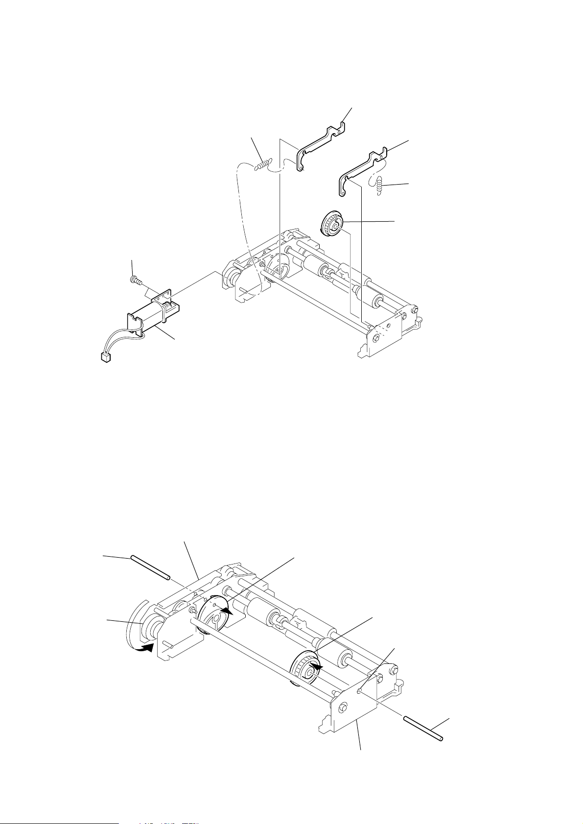
Phase adjusting of Feeder cam Assy
1) Remove each part in numerical order in the figure.
(Refer to Fig.2)
4 Feed lock
1 Two screws
3 Tension spring
2 Feeder motor Assy
6 Feed lock
5 Tension spring
7 Feeder cam (R) Assy
Fig.2
2) Rotate the gear (A) 8 in the direction of arrow, and pierce the
Pin (ø1) 9 through from a positioning hole on the reinforcement to the feeder cam (L) Assy. (Refer to Fig.3)
3) Pierce the Pin (ø1) 0 though a positioning hole on the side
plate (R) in the state of step 2), then install the feeder cam (R)
Assy 7. (Refer to Fig.3)
4) Pull out the two Pins (ø1) 9 and 0, then install each part 1
to 6 in reverse order of removing. (Refer to Fig.2)
Reinforcement
9 Pin (ø1)
8 Gear (A)
Feeder cam (L) Assy
7 Feeder cam (R) Assy
Positioning hole
0 Pin (ø1)
FIg.3
2-6 E
Side plate (R)
Page 19

SECTION 3
)
MECHANICAL ADJUSTMENTS
Replacing the Thermal Head
1) Before replacing the head, print the stair-step pattern with the
old head (faulty head).
Note 1: Only when the head is not entirely damaged with black or
white lines.
Note 2: To reproduce the stair-step pattern, refer to “Adjusting
Method 1” in “4. Electrical Adjustments”.
2) Remove the upper cabinet. (Refer to “2. Disassembly”.)
3) Remove the flat cables 1 (POHE13) and 2 (ADHE13) from
the thermal head. (Refer to Fig. 1)
4) Remove the two screws 3 (BVTT2.6 × 6) and remove the
harnesses 4 and fan holder 5. (Refer to Fig. 1)
5) Remove screw 6, (PS2.6 × 4) and remove the ribbon guide
7. (Refer to Fig. 2)
6) Remove the two screws 8 (PSW2.6 × 8) and remove the ther-
mal head 9 from the heat sink 0. (Refer to Fig. 2)
Note: Do not remove the screw qs fixing the heat sink 0 and head
arm qa.
7) Replace the thermal head 9.
Note: Make sure that the silicon grease (white) does not stick onto
the printing screen of the thermal head. If it does, remove with
alcohol.
8) Assemble in the reverse order of steps 2) to 6).
9) Perform “Head Voltage Adjustment” of “4. Electrical Adjustments” (Page 4-3).
5 fan holder
1 flat cable
(POHE13)
3 two screws
(BVTT2.6 × 6)
4 harness
2 flat cable
(ADHE13)
qs two screws
Note: Do not remove
0 heat sink
9 thermal head
the screw.
7 ribbon guide
Fig. 2
6 screw
(PS2.6 × 4)
8 two screws
(PSW2.6 × 8
qa head arm
Fig. 1
Confidential
3-1 E
DMP-1000P (AEP)
Page 20
SECTION 4
ELECTRICAL ADJUSTMENTS
During the adjustment, see the Adjustment and Adjustment Pats on page 4-7.
Pre-Adjustment Preparations
1. Equipment required
Electrical adjustment requires the following measuring equipment.
(1) Monitor TV
(2) Oscilloscope: 2 phenomena, bend 30 MHz or more, with de-
lay mode (use 10 : 1 probe unless otherwise specified)
(3) Frequency counter
(4) Pattern generator
(5) Digital voltmeter
(6) Video print paper
(7) Video print cartridge
(8) Vector scope
If S-VIDEO is designated
• If pattern generator does not provide Y/C separate
output terminals
Pattern Generator
VIDEO OUT
(75 Ω)
VTR with S-VIDEO terminal (E-E mode)
VIDEO IN
S-VIDEO OUT
2. Connection of Equipment
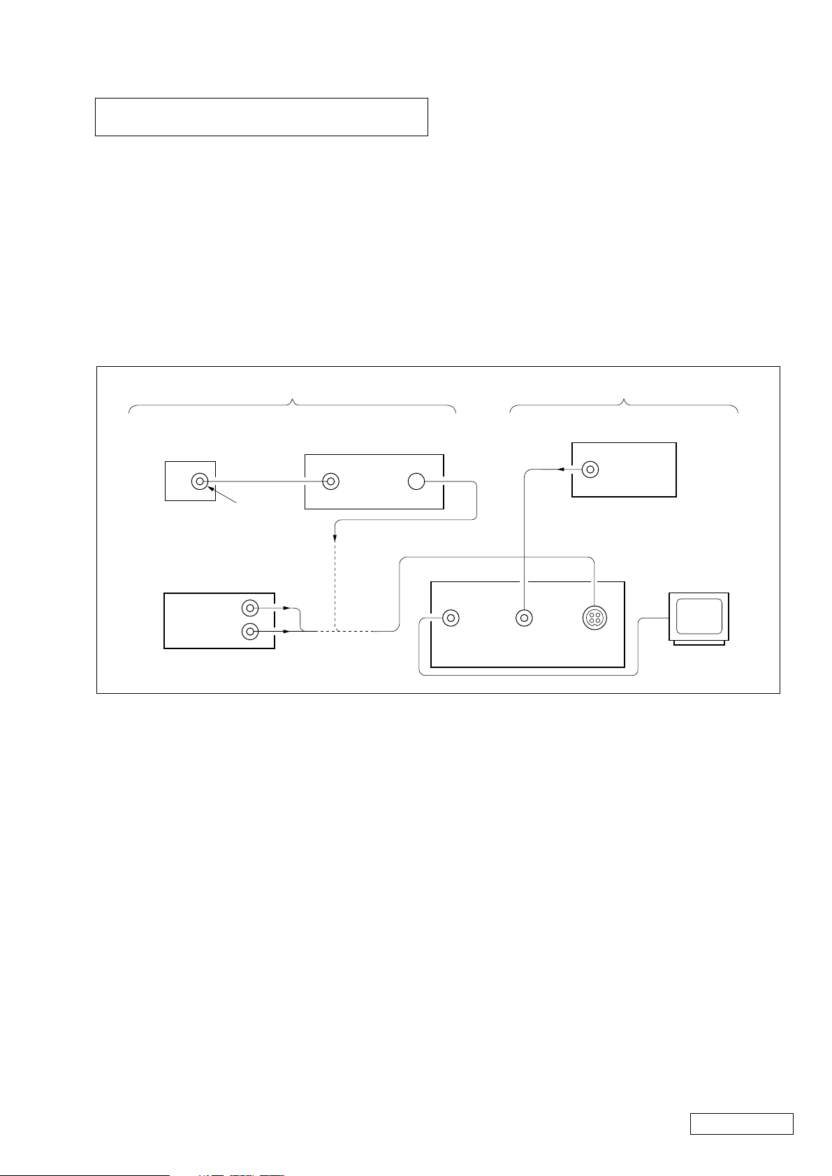
Following the designation of input terminal (S-VIDEO or VIDEO),
connect measuring units as shown in Fig. 4-1 and make adjustment.
The input terminal is designated with ( ) in the signal column.
Unless otherwise designated, either input terminal may be used.
Note: In the adjustment where the S-VIDEO input is designated, if ad-
justment was made with the VIDEO input. The specification of
this set will not be satisfied. Always follow the designation.
If adjustment was made using the VTR with S-VIDEO OUT terminal as a signal source, the performance of this set depends on that
VTR. Therefore, use the pattern generator with the Y/C separate
output terminals, if possible.
If VIDEO is designated
Pattern Generator
VIDEO OUT
(75 Ω)
• If pattern generator provide
Y/C separate output terminals
Pattern Generator
Y OUT (75 Ω)
Chroma OUT
(75 Ω)
VIDEO
OUT
Fig. 4-1
VIDEO IN
Set
Monitor TV
S-VIDEO
IN
4-1
Confidential
DMP-1000P (AEP)
Page 21

3. Input Signal Check
V
V
The video circuit adjustment uses as adjustment signals the video
signals obtained from the pattern generator, and therefore these
video output signals must be within the specification.
(1) When S-VIDEO is input
Connect an oscilloscope to the Y signal pin of the S-VIDEO IN
connector, and check that the sync signal of Y signal is 300 mV,
video amplitude is 700 mV, and the setup level is 0 mV. (If using
the VTR with S-VIDEO OUT terminal, check further that the
chroma signal and burst signal do not remain.)
Also, connect an oscilloscope to the chroma signal pin of the SVIDEO IN connector, and check that the burst signal amplitude of
chroma signal is 300 mV and it is flat, and moreover, the amplitude ratio of burst signal to chroma signal is 0.30 : 0.66. The Y
signal and chroma signal used for adjustment are shown in
Fig. 4-2.
Setup level: Potential difference between black and pedestal
(2) When VIDEO is input
Connect an oscilloscope to the VIDEO IN terminal, and check
that the sync signal amplitude of VIDEO signal is 300 mV, video
amplitude is 700 mV, the setup level is 0 mV, and the burst signal
amplitude is 300 mV and it is flat. Also, check that the level ratio
of burst signal to red signal is 0.3 : 0.66.
The VIDEO signal (color bars) used for adjustment is shown in
Fig. 4-3.
White (Approx. 100%)
Burst signal
Approx.
Approx.
0.3 V
0.7 V
Red
Horizontal sync signal
(To be flat)
Approx.
0.3 V
Y signal
White (100%)
Black
Approx. 700 mV
Pedestal
Horizontal
sync signal
Chroma signal
300 ± 10 m
Chroma
amplitude
Burstsignal
to be flat
Burst amplitude : chroma amplitude = 0.30 : 0.66
Fig. 4-2 Color bar signals of pattern generator
(at terminating resistance 75 Ω)
Fig. 4-3 Color bar signal of pattern generator
(at terminating resistance 75 Ω)
Approx.
300 m
Confidential
DMP-1000P (AEP)
4-2
Page 22
POWER SUPPLY BLOCK
[Head V oltage Adjustment]
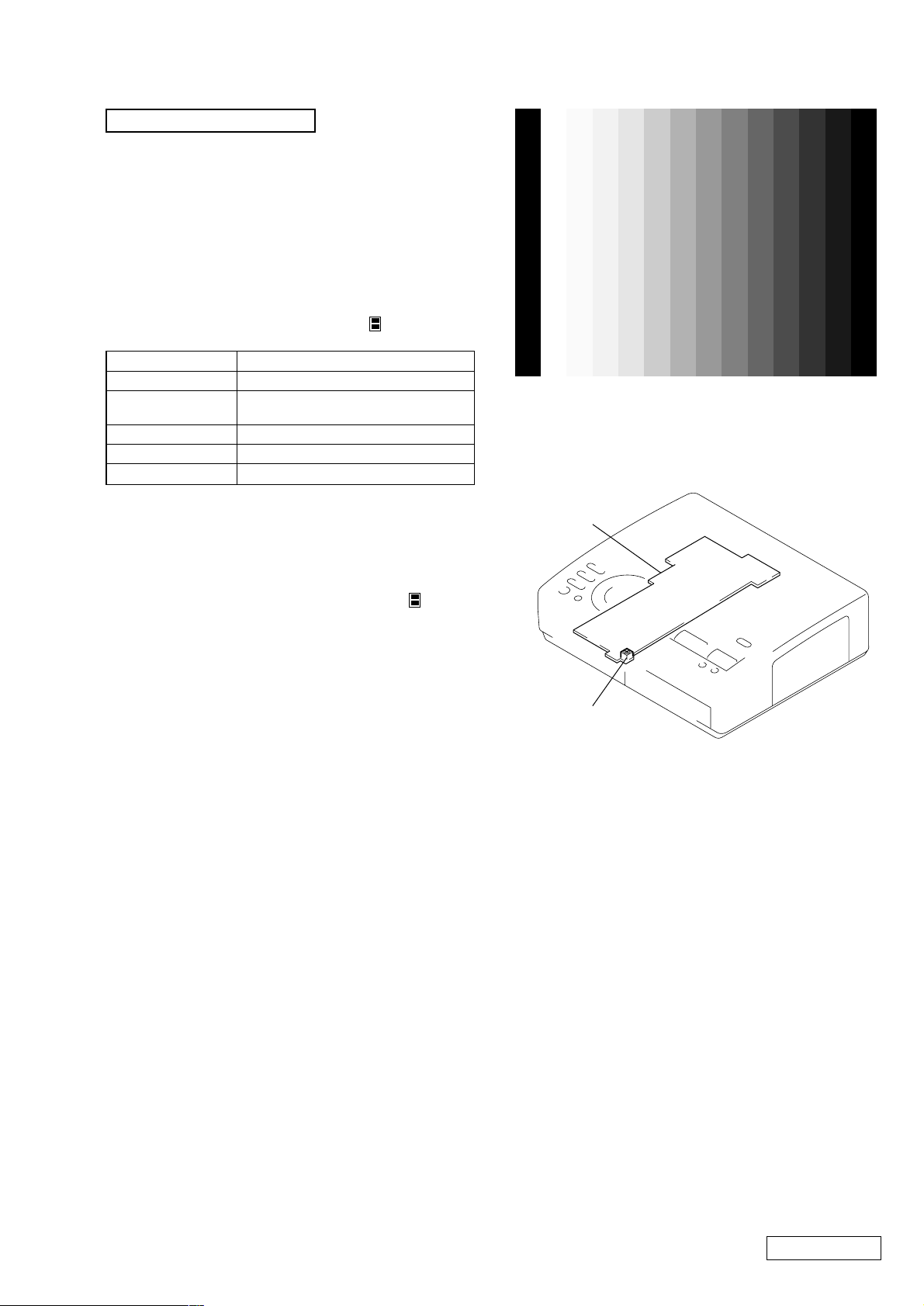
Before performing this adjustment, print the stair-step pattern
(Note 2) two times continuously with the old head (Note 1) or
normal unit. The second print will be used as a sample of the print
density.
Note 1: Only when the old head (faulty head) is not entirely damaged
with black or white lines.
Note 2: To print the stair-step test pattern, turn on the power switch while
pressing the S1714 (SAVE) and S1717 (ENTER) on the SW-39
board.
(Press the S1714 (SAVE) and S1717 (ENTER) until a peep is
heard.) Set the S1701 (Rotaly switch) to the position, and press
the S1706 (print), then the print will start.
Mode Test mode (Note 2)
Signal Test pattern (Stair-step)
Measuring points
Measuring instrument Digital Voltmerter
Adjustment part VR201
Specification Print density should be the same as the sample
+: CN1943 2 pin (MD-39 board)
–: CN1943 3 pin
Fig. 4-4 Stair-step pattern
* VR201 is in the power block (1-468-364-31).
Adjustment Location:
Adjustment Procedure:
(1) To print the stair-step test pattern, turn on the power switch
while pressing the S1714 (SAVE) and S1717 (ENTER) on
the SW-39 board.
(Press the S1714 (SAVE) and S1717 (ENTER) until a peep
is heard) Set the S1701 (Rotaly switch) to the position,
and press the S1706 (print), then the print will start.
(2) After printing, repeat (1) immediately.
(3) Compare the second printed pattern density with that of the
sample, and if the density differs, perform the following ad-
justment.
(4) Adjust VR201 according to the print density.
If darker than the sample: Decrease the head voltage.
If lighter than the sample: Increase the head voltage.
(5) Print the stair-step pattern two times continuously.
(6) Compare the second printed pattern density with that of the
simple, and if the density differs, repeat steps (3) to (6).
Note: Only one print is required after the second time.
(7) Turn off the power switch.
power block
VR201
4-3
Confidential
DMP-1000P (AEP)
Page 23

VIDEO BLOCK
[Free-Run Frequency Adjustment (1)] (VI-39 board)
Mode VIDEO Input
Signal Color bar (S-VIDEO IN) (Note 1)
Measuring point IC108 qk pin
Measuring equipment Frequency Counter
Adjustment part CT102
Specification value 4.433619 MHz ± 30 Hz
Note 1: Connect IC108 5 pin to the GND via 0.1µF capacitor (chroma
signal grounded.)
Adjustment Procedure:
(1) Connect IC108 7 pin to the GND via 1 MΩ resisitor.
(2) Adjust CT102 so that the frequency counter reading satisfies
the specification value.
[Free-Run Frequency Adjustment (2)] (DK-39E board)
Mode VIDEO Input
Signal Color bar (S-VIDEO IN)
Measuring point IC407 <zzc> pin
Measuring equipment Frequency Counter
Adjustment part CT500
Specification value 14.21875 MHz ± 100 Hz
Adjustment Procedure:
(1) Adjust CT500 so that the frequency counter reading satisfies
the specification value.
[910fh Adjustment] (DK-39E board)
Mode VIDEO Input
Signal Color bar (S-VIDEO IN)
Measuring point IC401 qa pin (or CL427)
Measuring equipment Digital Voltmeter
Adjustment part CT401
Specification value 2.5 ± 0.1 Vdc
Adjustment Procedure:
(1) Adjust CT401 so that the digital voltmeter reading satisfies
the specification value.
[Y/C Separation CHROMA Level] (VI-39 board)
Mode VIDEO Input
Signal Color bar (VIDEO IN)
Measuring point CL129
Measuring equipment Oscilloscope
Adjustment part RV102
Specification value 300 ± 5 mVp-p
Adjustment Procedure:
(1) Adjust RV102 so that the A level (white) of waveform on
the oscilloscope satisfies the specification value.
A
H
Fig. 4-6
[1H Delay Adjustment] (VI-39 board)
Mode VIDEO Input
Signal Color bar (S-VIDEO IN)
Measuring point FL106 3 pin
Measuring equipment Oscilloscope
Adjustment part RV105, 250, CT250
Adjustment Procedure:
(1) Set RV105 so that the luminescent spot of center.
(2) Set R V250 and CT250 so that the luminescent spots of phase
and gain.
[D/A Output Y Level Adjustment] (DK-39E board)
Note: Turn of the power switch once, then turn it on again.
Mode VIDEO Input
Signal Color bar (VIDEO IN)
Measuring point J1802 (OUTPUT)
Measuring equipment Oscilloscope
Adjustment part RV401
Specification value 700 ± 5 mVp-p
[Y/C Separation Y Level Adjustment] (VI-39 board)
Mode VIDEO Input
Signal Color bar (VIDEO IN)
Measuring point CL138
Measuring equipment Oscilloscope
Adjustment part RV103
Specification value 700 ± 10 mVp-p
Adjustment Procedure:
(1) Adjust RV103 so that the A level (white) of waveform on
the oscilloscope satisfies the specification value.
White (100%)
A
H
Fig. 4-5
Confidential
DMP-1000P (AEP)
Adjustment Procedure:
(1) Adjust RV401 so that the A level (white) of waveform on
the oscilloscope satisfies the specification value.
White (100%)
A
H
Fig. 4-7
4-4
Page 24

[D/A Output CHROMA Level Adjustment] (DK-39E board)
Mode VIDEO Input
Signal Color bar (VIDEO IN)
Measuring point J1802 (OUTPUT)
Measuring equipment Oscilloscope
Adjustment part RV402
Specification value 681 ± 5 mVp-p
Adjustment Procedure:
(1) Adjust R V402 so that the A level (Red) of waveform on the
oscilloscope satisfies the specification value.
(2) Turn off the power switch.
White (100%)
A
[A/D Input R-Y/B-Y Level Adjustment]
(VI-39, DK-39E board)
Mode VIDEO Input
Signal Color bar (S-VIDEO IN)
Measuring point CL407, 408
Measuring equipment Oscilloscope
Adjustment parts RV106, 405
Specification value
CL407 (R-Y) 1.05 ± 0.01 Vp-p
CL408 (B-Y) 1.20 ± 0.01 Vp-p
Adjustment Procedure:
(1) Connect on oscilloscope to the CL408.
(2) Adjust RV106 so that the A level (B-Y) of waveform on the
oscilloscope satisfies the specification value.
Blue
H
Red
Fig. 4-8
[A/D Input Y Level Adjustment] (DK-39E board)
Note: Turn off the power switch once, then turn it on again.
Mode VIDEO Input
Signal Color bar (S-VIDEO IN)
Measuring point CL409
Measuring equipment Oscilloscope
Adjustment part RV404
Specification value 1.30 ± 0.01 Vp-p
Adjustment Procedure:
(1) Connect on oscilloscope to the CL409 (from IC407 yf pin
to the point via R478).
(2) Adjust RV404 so that the A level (white) of waveform on
the oscilloscope satisfies the specification value.
White (100%)
A
H
A
Yellow
Fig. 4-10
(3) Connect on oscilloscope to the CL407.
(4) Adjust RV405 so that the A level (R-Y) of waveform on the
oscilloscope satisfies the specification value.
Red
Yellow
A
Fig. 4-11
Fig. 4-9
4-5
Confidential
DMP-1000P (AEP)
Page 25

[HUE Level Adjustment] (VI-39 board)
Mode VIDEO Input
Signal Color bar (S-VIDEO IN)
Measuring point J1802 (OUTPUT)
Measuring equipment Vector scope
Adjustment part RV105
Specification value Yellow phase 167 ± 4 deg
Adjustment Procedure:
(1) Connect on vector scope to the J1802.
(2) Press the S1707 (CAPTURE).
(3) Check yellow phase satisfies the specification value.
(4) If NG, press the S1708 (PICTURE) and lights on the D1733
(INPUT)
(5) A little adjust the RV105 and press the S1707.
(6) Repeat steps (2) to (5) until yellow phase satisfies the speci-
fication value.
90 °
167 ± 4 °
180 °
Yellow
Fig. 4-12
Reference : B-Y Waveform (CL408)
•
•
Fig. 4-13
0 °
A
If yellow phase is under 163 °,
extend the A level.
If yellow phase is over 171°,
shorten the A level.
Confidential
DMP-1000P (AEP)
4-6
Page 26

Adjustment Parts and Measuring Points:
– DK-39E Board (side A) –
RV404
A/D Input Y Level
Adjustment
RV405
A/D Input R/Y Level
Adjustment
CT401
910fh Adjustment
CN501 CN503
176 133
1 132
IC503
IC407
8944
8845
– DK-39E Board (side B) –
CL408
CL407
CL409
CL427
RV401
D/A Output Y Level
Adjustment
IC401
RV402
D/A Output Chroma Level
Adjustment
CT500
Free-run Frequency (2)
Adjustment
IC506
IC505
4-7
Confidential
DMP-1000P (AEP)
Page 27

– VI-39 Board (side A) –
j
CN102
20 1
1
3
FL106
RV105
HUE Level Adjustment
CT102
Free-Run Frequency (1)
Adjustment
IC108
RV106
A/D Input B/Y Level
ustment
Ad
– VI-39 Board (side B) –
– MD-39 Board (component side) –
CT250 RV250
1H Delay Adjustment
RV102
Y/C Separation Chroma Level
Adjustment
CL138
CL129
RV103
Y/C Separation Y Level
Adjustment
– VS-39 Board (component side) –
Confidential
DMP-1000P (AEP)
CN1943
4
1
J1802
OUTPUT
4-8
4-8 E
Page 28

5-1. BLOCK DIAGRAM – VIDEO Section –
J1801
VIDEO
INPUT
VIDEO AMP
Q104, 123
CLAMP
Q124
RV102
Y/C SEPARATION
CHROMA LEVEL
RV103
Y/C SEPARATION
Y LEVEL
SECTION 5
DIAGRAMS
Y/C SEPARATOR
IC105
AD IN
25
41
CVRF
YVRF
33
INSL
10
11
AYO
ACO
OCLK
37
YMCK
17
YO
16
CT410
910fh
Y BUFFER
Q412
R-Y BUFFER
Q411
MCKO
AFH
WEVN
26
VD
27
32
2
IC402
4
R-Y
Y/C MIX
IC103 (1/2)
31
39
Y IN
18
Y/C
MIX
C IN
17
VIDEO
AMP
C VIDEO
OUT
R-Y
J1802
OUTPUT
LOW-PASS
FILTER
FL105
LOW-PASS
FILTER
FL106
20
Y AMP
Q403
R-Y AMP
Q404
LOW-PASS
FILTER
Q401, 416
RV404
A/D IN
Y LEVEL
RV405
A/D IN
R-Y LEVEL
R-Y
VSIN
5
VCIN
9
Y BUFFER
Q407
R-Y BUFFER
Q406
AFC
IC401
MCKI
BFP
15
23
CLAMP
Q410
CLAMP
Q408
ECK
90
EVD
88
EHD
89
EEVN
91
A/D, D/A CONVERTER,
MEMORY BUS CONTROL
IC407 (1/2)
Y IN
64
V IN
82
CJ1801
S VIDEO INPUT
1
3
4
2
(ON: PLUG IN)
R-Y OUT
20
B-Y OUT
19
RV401
D/A OUT
Y LEVEL
RV402
D/A OUT
CHROMA LEVEL
B-Y
R-Y
B-Y
73
U IN
VREF1
26
VREF2
33
VREF3
40
B-Y
Y SIGNAL
SELECT SWITCH & VIDEO AMP
Y
C
3
1
3
1
IC102
5
2
SELECT SWITCH & VIDEO AMP
2 5 4
4
CHROMA SIGNAL
IC101
1
1H DELAY
IC250
IN
CLK IN
5
OUT
3
CLOCK BUFFER
R-Y/B-Y DECODER
IC108
7
7
LOW-PASS
FILTER
FL102
BAND-PASS
FILTER
FL101
Y AMP
Q107
CHROMA
AMP
Q109
VIDEO
25
C IN
5
C OUT
3
Q113
AMP
Q251
LOW-PASS
FILTER
FL107
RV250
1H DELAY
CT250
1H DELAY
CT102
FREE-RUN
FREQUENCY (1)
LOW-PASS
FILTER
FL250
VCXI
12
B-Y AMP
Q402
B-Y
BUFFER
Q252
AMP
Q250
X101
17.73MHz
VCXO
10
B-Y BUFFER
Q405
DEMODULATOR
FL251
RV106
A/D IN
B-Y LEVEL
C CNT
4
B-Y
R-Y
B-Y
HUE LEVEL
RV105
CLAMP
Q409
R-Y
16
14
11
T IN
R-Y IN
B-Y IN
B-Y BUFFER
Q413
24
HD
• SIGNAL PATH
: COMPOSITE VIDEO
: Y SIGNAL
: CHROMA SIGNAL
R-Y
: R-Y SIGNAL
B-Y
: B-Y SIGNAL
05
VIDEO ENCODER
IC103 (2/2)
Y OUT
16
R-Y
MODULATOR
C OUT
15
+
PULSE
GENERATOR
B-Y
MODULATOR
PHASE
SHIFTER
CLAMP
CLAMP
CLAMP
OSC
Y IN
R-Y IN
B-Y IN
XO IN
XO OUT
C SYNC IN
10
4
2
3
6
5
X102
4.43MHz
R-Y
B-Y
Y BUFFER
R-Y BUFFER
Q102 (1/2)
B-Y BUFFER
Q102 (2/2)
CT103
ENCODER
4.43MHz
Q101
5-1 5-2
R-Y
B-Y
Y OUT
29
V OUT
43
36
U OUT
SYCX
20
50
CGEEX
Confidential
DMP-1000P (AEP)
Page 29

5-2. BLOCK DIAGRAM – MAIN Section –
RESET
A
(Page 5-6)
RESET
B
(Page 5-7)
4
IC502
RESET SWITCH
TIMER
IC1700
VDD
14
WR
CE
CLK
1
2
RESET SIGNAL
GENERATOR
IC501
D513
+5V
BUFFER
Q2000
11
DATA
6812
D1750
BT1700
LITHIUM
BATTERY
+5V
BZ201
(BUZZER)
CT500
FREE-RUN
FREQUENCY (2)
X503
7.159MHz
D-RAM
IC403
UCAS
LCAS
RAS
WE
I/O0 – I/O15
A0 – A9
51
RESX
ICKI
113
108 101
SHWX
104
BSH
STRS
103
SVBK
MDT0 – MDT15
2 – 5, 7 – 10, 33 – 36, 38 – 41
17 – 20, 23 – 28
30
31
14
13
160 – 167, 170 – 176, 116 – 13, 11 – 6
A/D, D/A CONVERTER,
MEMORY BUS CONTROL
MAD0 – MAD9
MCSX
124
MRSX
123
MWEX
125
IC407 (2/2)
VRSR
SVW
SC6X
SWEX
SRDX
SRSX
SCSX
102
100
99
107
106
105
109
110
1/2 DIVIDER
IC406
CS6
WR
RD
RD
WE
RAS0
HCAS
3
6
11
8
4
107
1
5
67
3
4
SWITCHING
IC513 (1/4)
SWITCHING
IC513 (2/4)
SWITCHING
IC513 (3/4)
SWITCHING
IC513 (4/4)
SWITCHING
IC511
CK
WAIT
BSH
VTRS
VBLK
VRSR
VWR
2
1
4
5
12
13
10
9
1
2
44
XWDTOVF
4
108
IC510
XRES
46
45
132
TIMER CE
TIMER WR
TIMER SCR
TIMER RXD
118
S1706 – 1708,
S1710 – 1715, 1717, 1718
KEY0
KEY1
119
KEY2
120
ROTARY
SWITCH
S1701
(FUNCTION SELECT)
MINI
JACK
BLOCK
41 51
130
SWAY COMPEN
FD/VIDEO SEL
131
TIMER TXD
SYSTEM CONTROLLER
IC503 (1/3)
XRAS
XCASH32XCASL
XCS0
1
2
LATCH
IC514
QD
CK
Q
2
IC515
1
4
5
3
RAS-CNT
RDWR
34
2
XRD
XWR
FLASH
4850 36 31 43143
57
S1719
INPUT SELECT
VIDEO MOTION
VIDEO STILL
REMOTE
CAPTURE
FD
WR
RD
110
BUZZER
D0 – D15
92 – 88, 86, 84 – 80,
78, 76 – 73
D0 – D15
D0 – D15
A1 – A12
A0 – A17
7 – 11, 13,
15 – 25, 27
A0 – A17
ADDRESS BUS
DATA BUS
94
96
XTL
EXTL
(Page 5-7)
F
(Page 5-7)
G
PCS
C
(Page 5-7)
WR, RD
D
(Page 5-5)
WR, RD
E
(Page 5-7)
05
Confidential
DMP-1000P (AEP)
DATA BUS
PCSX
97
RD
36
OE
WE
UCAS
LCAS
RAS
ADDRESS BUS
DATA BUS
WE
13
37
38
14
A13
RD
WR
30
32
7
CE
OE
WE
DQ0 – DQ7
21 – 23, 25 – 29
D0 – D7
FLASH MEMORY
IC506
20 – 13, 3, 2, 31, 1,
12, 4, 5, 11, 10, 6
ADDRESS BUS
A0 – A17
A0 – A17
DATA BUS
5-4
SDT0 – SDT15
SADA, SADB
SAD0 – SAD11,
D0 – D15
157 – 150, 147 – 140138 – 127, 121, 120
A1 – A14
5-3
DATA BUS
ADDRESS BUS
D0 – D15
2 – 5, 7 – 10,
41 – 44, 46 – 49
D0 – D15
D-RAM
IC509
A0 – A11
19 – 24, 27 – 32
A1 – A12
ADDRESS BUS
D0 – D7
A0
H
I
(Page 5-5)
(Page 5-5)
Page 30

5-3. BLOCK DIAGRAM – FLOPPY DISK DRIVE CONTROL/EEPROM Section –
CN2100
READYO
INDEX
STEP
TRACK 00
10
9
6
4
8
X2100
16MHz
82
2
12
14
16
18
20
22
24
26
INDEX
76
8
DIR
10
STEP
WDATA
11
WE
13
TRK0
24
WPRT
26
27
RDATA
36
SIDE
XB186XA283XA1
FLOPPY DISK DRIVE CONTROLLER
RD
46 47
RD
WR
IC2101
WR
57 – 60, 62, 63, 65, 67
D0 – D7
D0 – D7
READY
INT
RESET
DMAAK
DMARQ
A0
51
A0
30
71
45
TC
70
CS
50
69
68
TO FLOPPY DISK
DRIVE UNIT
(Page 5-3)
MOTOR ON
DENSITY OUT
DISK CHANGE
DRIVE SELECT 0
DIRECTION
WRITE DATA
WRITE GATE
WRITE PROTECT
READ DATA
SIDE1 SELECT
WR, RD
D
BUFFER
Q2100
IC2102
D2100
42
SYSTEM CONTROLLER
116
FDD MOTOR ON
115
FDD DENSITY OUT
114
FDD DISK CHANGE
113
FDD DRIVE SELECT 0
FDD READY OUT
72
FDD READY IN
144
39
FDC INT
69
RESET FDC
FDC TC
137
FDC CS
53
FDC DMA ACK
59
FDD DMA RQ
109
IC503 (2/3)
EEPROM RESET
EEPROM CS
EEPROM SCK
EEPROM RXD
EEPROM TXD
VCC/FWP
MD1/BOOT
PD
PD
33
30
29
136
133
134
99
102
BUFFER
IC2001
7
3
1
6
BUFFER
IC2000
7
5
1
2 6
5
2
3
1
8
RST
3
CS
CLK
4
EEPROM
IC2002
6
DO
5
DI
CN551
5
RA2
4
DA
7
8
6
FWP
MD1
RESET
FOR CHECK
(Page 5-4)
(Page 5-4)
D0 – D7
H
A0
I
05
DATA BUS
ADDRESS BUS
RESET
A
(Page 5-3)
Confidential
5-5
5-6
DMP-1000P (AEP)
Page 31

5-4. BLOCK DIAGRAM
– HEAD/SENSOR/MOTOR/POWER SUPPLY Section –
HEAD CONTROLLER,
MECHANISM CONTROLLER
IC505
D0 – D15
A1 – A12
RESET
WR, RD
PCS
MIRROR IMAGE
S1720
DATE
D1731
POWER
D1736
INDICATOR
D1734
MEMORY
D1733
INPUT
D1735
RIBBON ERROR
INDICATOR
05
S1702
SELECT
OFF
ON
LED DRIVE
Q1731
WR
DT0 – DT15
71 – 64, 61 – 54
51 – 40
AD1 – AD10,
REGX, CUTEX
35
RESX
37
RD
WEX
RDX
36
39
CS1X
MAVICA PRINT
92
PC
91
DATE (PWSW)
82
POWER-LED
80
79
PAPER-LED
PRN-LED
77
MEM-LED
76
INP-LED
75
74
RIBBON-LED
XIN14XOUT
13
X502
20MHz
5-7
Confidential
DMP-1000P (AEP)
F
(Page 5-4)
G
(Page 5-4)
B
(Page 5-3)
E
(Page 5-3)
C
(Page 5-3)
H
V
OFF
PAPER REPLACEMENT
D1737 – 1739
PRINTING STATUS
INDICATOR
PDT0
PDT1
PDT2
PDT3
HDCK
LATX
DRVX
HPS0
HPS1
RCODE0
RCODE1
RCODE2
STPLOW
FAN
RMTRCCW
RMTRCW
HMTRCCW
HMTRCW
FKEY0
FKEY1
FKEY2
FMTRCW
FMTRCCW
FPS
FEEDER
23
22
21
20
25
24
19
5
6
98
97
96
81
83
90
89
87
86
1
100
99
84
85
3
2
HEADTMP
121
1
HEAD
POSITION
SENSOR AMP
IC508
7
HEAD UP/DOWN MOTOR DRIVE,
RIBBON MOTOR DRIVE
IN4
10
IN3
7
IN2
2
IN1
15
SHEET BIT0
SHEET BIT1
SHEET BIT2
FE MOTOR 0
FE MOTOR 1
FE POSITION
SENSE
FE DESORPTION
SENSE
3
5
HEAD FAN
MOTOR DRIVE
Q1900
IC1900
MOTOR
DRIVE
MOTOR
DRIVE
CN1882
5
6
7
4
3
2
1
HEAD901
THERMAL HEAD
TH
DATA1
DATA2
DATA3
DATA4
CLOCK
LATCH
STROBE
HEAD POSITION 0
SENSOR
PH1852
HEAD POSITION 1
SENSOR
PH1851
RIBBON CODE 0
SENSOR
PH906
RIBBON CODE 1
SENSOR
PH905
RIBBON CODE 2
SENSOR
PH904
OUT4
11
OUT3
6
OUT2
3
OUT1
14
M
(HEAD FAN)
M903
M
(RIBBON)
M
(HEAD UP/DOWN)
CN201
5
6
7
4
3
2
1
M901
M902
A0
A1
A2
PAPER EDGE
SENSOR
PH901
JAMMING
DETECT SENSOR
PH1861
RIBBON MARK 0
SENSOR
PH902
RIBBON MARK 1
SENSOR
PH903
COMPARATOR
IC100
RMARK1
RMARK0
PPEDG
JDET
122
126125123
AUTOMATIC FEEDER UNIT
ENCODER
IC101
A0
9
A1
7
A2
6
FEEDER MOTOR DRIVE
IC102
IN1
OUT1
3
OUT2
4
IN2
+5V
SYSTEM CONTROLLER
IC503 (3/3)
STP4
STP3
STP1
STP2
142
140 139
138
1
14
+5V
IN0
10
11
–
IN1
13
–
IN7
9
7
FEEDER POSITION SENSOR
ROTARY
.
SWITCH
1
4
–
M
S100
SHEETS SET
M101
(FEEDER)
SELECTOR
IC1903
1
2
4
5
12
13
9
10
COMPARATOR
IC1902 (1/2)
COMPARATOR
IC1902 (2/2)
3
6
11
8
4
5
10
11
PLATEN MOTOR DRIVE
IC1901
SWITCH
2
SWITCH
6
SWITCH
4
8
SWITCH
10 1
+5V
HIGH/LOW
SPEED SWITCH
Q1902
RIBBON CODE SENSOR LED
(PH904 – 906) B+
MOTOR +22V
3
7
5
9
M905
(POWER FAN)
+5V
FLOPPY DISK DRIVE
UNIT B+
VIDEO CIRCUIT B+
A/D, D/A CONVERTER (IC407),
VIDEO CIRCUIT B+
+5V (DIGITAL SYSTEM)
SYSTEM CONTROLLER (IC503),
HEAD/MECHANISM
CONTROLLER (IC505) B+
S1871
(RIBBON DOOR DETECT)
M
+5V
5-8
M
M904
(PLATEN)
+5V
LED DRIVE
Q1903
+5V
+22V MOTOR B+
+7V MOTOR B+
+6.25V SIGNAL B+
+5V
REGULATOR
IC2100
+5V
REGULATOR
IC110
+5V
REGULATOR
IC404
+5V
REGULATOR
IC504
POWER
BLOCK
POWER
(AC IN)
Page 32

5-5. FRAME SCHEMATIC DIAGRAM
SW-39
MINI JACK
BLOCK
POWER FAN
VI-39
05
CN1701
D GND
22
CLK
21
DATA
20
WR
19
CE
18
G_GND
SWAY COMPEN
MAVICA PRINT
POWER
MEMORY
RIBBON
PAPER-IN
D GND
M905
+6.25V S
+6.25V S
VIDEO/AVLINK
Y. VA OUT
R-Y. VA OUT
B-Y. VA OUT
V OUT GND
VIN GND
S IN GND
S/V SEL
17
16
KEY0
15
KEY1
14
KEY2
13
FD
12
PC
11
10
DATE
D GND
INPUT
PRINT
D +5V
KEY 0
KEY 1
GND S
GND S
A GND
CGFFX
A GND
A GND
A GND
A GND
V OUT
1
2
3
GND
+5V
CN102 CN401
HD
10
11
12
DA. V
13
DA. U
14
DA. Y
15
16
SYNC
17
18
SC
19
20
CN101
V IN
Y
C
9
8
7
6
5
4
3
2
1
BLK
RED
1
2
3
4
5
6
7
8
9
1
2
3
4
5
6
7
8
SWDK22
(FFC)
VIDK20
(FFC)
VIVS8
(FFC)
22
21
20
19
18
17
16
15
14
13
12
11
10
9
8
7
6
5
4
3
2
1
1
2
3
1
2
20
19
18
17
16
15
14
13
12
11
10
9
8
7
6
5
4
3
2
1
8
7
6
5
4
3
2
1
CN504
CN2000
CN402
CN1801
VS-39
D GND
CLK
DATA
WR
CE
D GND
SWAY COMPEN
KEY0
KEY1
KEY2
FD
PC
MAVICA PRINT
DATE
D GND
POWER
INPUT
MEMORY
RIBBON
PAPER-IN
PRINT
D +5V
KEY 0
KEY 1
D GND
GND (POWER FAN)
+5V (POWER FAN)
+6.25V S
+6.25V S
VIDEO/AVLINK
GND S
GND S
HD
A GND
Y. VA OUT
R-Y. VA OUT
B-Y. VA OUT
CGFFX
A GND
DA. V
DA. U
DA. Y
A GND
SYNC
A GND
SC
A GND
V OUT
V OUT GND
V IN
V IN GND
Y
S IN GND
C
S/V SEL
HEAD901
HEAD901
FLOPY DISK
DRIVE UNIT
THERMAL
HEAD
(1/2)
(2/2)
CN1651 CN701
SIDE 1 SELECT
READ DATA
WRITE PROTECT
TRACK 00
WRITE GATE
WRITE DATA
DIRECTION
MOTOR ON
DENSITY OUT
READYO
DISK CHENGE
DRIVE SELECT 0
DATA1
LATCH
DATA2
CLOCK
STROBE
GND (TH)
GND (TH)
GND (TH)
GND (TH)
GND (TH)
GND (TH)
+22V (VTH)
+22V (VTH)
+22V (VTH)
+22V (VTH)
+22V (VTH)
+22V (VTH)
GND
GND
GND
GND
GND
NC
STEP
NC
NC
NC
+5V
+5V
INDEX
+5V
NC
GND
VDD
26
25
24
23
22
21
20
19
18
17
16
15
14
13
12
11
10
9
8
7
6
5
4
3
2
1
1
TH
2
TH
3
4
5
6
7
8
9
10
12
11
10
9
8
7
6
5
4
3
2
1
DKFD-26
(FFC)
ADHE13
(FFC)
POHE13
(FFC)
DK-39E FE-39
26
25
24
23
22
21
20
19
18
17
16
15
14
13
12
11
10
9
8
7
6
5
4
3
2
1
10
9
8
7
6
5
4
3
2
1
SIDE 1 SELECT
GND
READ DATA
GND
WRITE PROTECT
GND
TRACK 00
GND
WRITE GATE
GND
WRITE DATA
STEP
DIRECTION
MOTOR ON
DENSITY OUT
READY0
DISK CHENGE
+5V
DRIVE SELECT 0
+5V
INDEX
+5V
CN2100
CN502
DATA1
LATCH
GND
DATA2
CLOCK
-5V (DIGITAL)
STROBE
+5V (DIGITAL)
GND (MOTOR)
GND (MOTOR)
+7V (MOTOR)
+7V (MOTOR)
COUNT BIT2
COUNT BIT1
COUNT BIT0
FE MOTOR 0
FE MOTOR 1
FE POSI SENS
FE ON/OFF SENS
GND (DIGITAL)
NC
NC
NC
NC
HEAD FAN CONT
PAPER EDGE SENS
RIBBON MARK1 SENS
RIBBON MARK0 SENS
HEAD MOTOR IN1
HEAD MOTOR IN0
RIBBON MOTOR IN1
RIBBON MOTOR IN0
STEP MOTOR IN4
STEP MOTOR IN3
STEP MOTOR IN2
STEP MOTOR IN1
HIGH/LOW
+6.25V (SIGNAL)
+6.25V (SIGNAL)
+6.25V (SIGNAL)
GND (SIGNAL)
GND (SIGNAL)
GND (SIGNAL)
+5V (SIGNAL)
+7V (MOTOR)
+7V (MOTOR)
TH
TH
NC
GND (MOTOR)
GND (MOTOR)
RIBBON CODE2 SENS
RIBBON CODE1 SENS
RIBBON CODE0 SENS
HEAD POSI1 SENS
HEAD POSI0 SENS
JD SENS
1
2
3
4
5
6
7
8
9
10
11
12
13
ADFE13
(FFC)
CN501 CN1936
30
29
28
27
26
25
24
23
22
21
20
19
18
17
16
15
14
13
12
11
10
9
8
7
6
5
4
3
2
1
FP-700
FLEXBLE
(
(
BOARD
POWER BLOCK
GND (TH)
1
GND (TH)
2
GND (TH)
3
GND (TH)
4
GND (TH)
5
GND (TH)
6
+22V (VTH)
7
+22V (VTH)
8
+22V (VTH)
9
+22V (VTH)
10
+22V (VTH)
11
+22V (VTH)
12
+22V (MOTOR)
+22V (MOTOR)
GND (MOTOR)
GND (MOTOR)
GND (MOTOR)
GND (MOTOR)
+7V (MOTOR)
+7V (MOTOR)
GND (SIGNAL)
GND (SIGNAL)
+6.25V (SIGNAL)
+6.25V (SIGNAL)
+22V CONT
GND (FAN)
1
2
3
4
5
6
7
8
9
10
11
12
13
14
PS-33
CN1881CN503
+5V (DIGITAL)
13
GND (MOTOR)
12
GND (MOTOR)
11
+7V (MOTOR)
10
+7V (MOTOR)
9
COUNT BIT2
8
COUNT BIT1
7
COUNT BIT0
6
FE MOTOR 0
5
FE MOTOR 1
4
FE POSI SENS
3
FE ON/OFF SENS
2
GND (DIGITAL)
1
HEAD FAN CONT
1
PAPER EDGE SENS
2
RIBBON MARK1 SENS
3
RIBBON MARK0 SENS
4
HEAD MOTOR IN1
5
HEAD MOTOR IN0
6
RIBBON MOTOR IN1
7
RIBBON MOTOR IN0
8
STEP MOTOR IN4
9
STEP MOTOR IN3
10
STEP MOTOR IN2
11
STEP MOTOR IN1
12
HIGH/LOW
13
+6.25V (SIGNAL)
14
+6.25V (SIGNAL)
15
+6.25V (SIGNAL)
16
GND (SIGNAL)
17
GND (SIGNAL)
18
GND (SIGNAL)
19
+5V (SIGNAL)
20
+7V (MOTOR)
21
+7V (MOTOR)
22
GND (MOTOR)
23
GND (MOTOR)
24
RIBBON CODE2 SENS
25
RIBBON CODE1 SENS
26
RIBBON CODE0 SENS
27
HEAD POSI1 SENS
28
HEAD POSI0 SENS
29
JD SENS
30
CN1937
+22V (MOTOR)
1
+22V (MOTOR)
2
GND (MOTOR)
3
GND (MOTOR)
4
GND (MOTOR)
5
GND (MOTOR)
6
+7V (MOTOR)
7
+7V (MOTOR)
8
GND (SIGNAL)
9
GND (SIGNAL)
10
+6.25V (SIGNAL)
11
+6.25V (SIGNAL)
12
+22V CONT
13
GND (FAN)
14
MD-39
JUMMING DET SENS
RIBBON CODE2 SENS
RIBBON CODE1 SENS
RIBBON CODE0 SENS
RIBBON MARK0 LED
RIBBON MARK1 LED
RIBBON MARK1 SENS
RIBBON MARK0 SENS
RIBBON DOOR SENS12
CN1882
GND (DIGITAL)
GND (DIGITAL)
GND (DIGITAL)
+5V (DIGITAL)
GND (MOTOR)
GND (MOTOR)
+7V (MOTOR)
+7V (MOTOR)
COUNT BIT2
COUNT BIT1
COUNT BIT0
FE MOTOR 0
FE MOTOR 1
FE POSI SENS
FE ON/OFF SENS
+24V (MOTOR)
+24V (MOTOR)
RIBBON MOTOR X
RIBBON MOTOR Y12
HEAD MOTOR X
HEAD MOTOR Y
+22V (MOTOR)
JUMMING DET LED
GND (DIGITAL)
RIBBON CODE2 LED
RIBBON CODE1 LED
RIBBON CODE0 LED
GND (DIGITAL)
GND (DIGITAL)
PAPER EDGE LED
PAPER EDGE SENS
GND (DIGITAL)
GND (DIGITAL)
HEAD POSI 1 SENS
HEAD POSI 1 LED
HEAD POSI 0 LED
HEAD POSI 0 SENS
+5V (DIGITAL)
+5V(HEAD FAN)
FAN (HEAD FAN)12
15
14
13
12
11
10
9
8
7
6
5
4
3
2
1
CN1942
6
5
4
φ1
3
φ2
2
φ3
1
φ4
CN1941
CN1940
1
2
3
1
2
3
CN1933
1
2
3
4
5
6
7
CN1934
1
2
3
4
5
6
7
8
CN1931 CN1851
5
4
3
2
1
CN1932
CN1938
AUTOMATIC FEEDER UNIT
FJ-23
GND (DIGITAL)
15
GND (DIGITAL)
14
GND (DIGITAL)
13
+5V (DIGITAL)
12
GND (MOTOR)
11
GND (MOTOR)
10
+7V (MOTOR)
9
+7V (MOTOR)
8
COUNT BIT2
7
COUNT BIT1
6
COUNT BIT0
5
FE MOTOR 0
4
FE MOTOR 1
3
FE POSI SENS
2
FE ON/OFF SENS
1
+24V (MOTOR)
WHT
+24V (MOTOR)
FP-702
FLEXBLE
(
BOARD
FP-703
FLEXBLE
(
BOARD
HMD-3
RD-33
RM-33
HM-33
JD-33
RED
BLU
YEL
BRN
(
(
φ1
φ2
φ3
φ4
RIBBON MOTOR +
1
RIBBON MOTOR –
2
HEAD MOTOR +
1
HEAD MOTOR –
2
CN1861CN1935
JUMMING DET SENS
1
JUMMING DET LED
2
GND (DIGITAL)
3
RIBBON CODE2 SENS
1
RIBBON CODE2 LED
2
RIBBON CODE1 SENS
3
RIBBON CODE1 LED
4
RIBBON CODE0 SENS
5
RIBBON CODE0 LED
6
GND (DIGITAL)
7
RIBBON MARK & PE
GND (DIGITAL)
1
PE LED
2
PE SENS
3
RM 0 LED
4
RE 1 LED
5
GND (DIGITAL)
6
RM 1 SENS
7
RM 0 SENS
8
GND (DIGITAL)
5
HEAD POSI 1 SENS
4
HEAD POSI 1 LED
3
HEAD POSI 0 LED
2
HEAD POSI 0 SENS
1
CN1871
+5V (DIGITAL)
1
RIBBON DOOR SENS
2
+5V (DIGITAL)
+
FAN (HEAD)
–
FE MOTOR 1
FE MOTOR 0
FE POSI SENS
SHEET BIT0
+5V (DIGITAL)
SHEET BIT1
GND (DIGITAL)
SHEET BIT2
+7V (MOTOR)
+7V (MOTOR)
GND (MOTOR)
GND (MOTOR)
PLATEN MOTOR
RIBBON MOTOR
HEAD MOTOR
JD-39
RCODE
HP-39
RD-39
HEAD FAN
M904
M903
M902
M901
FR-23
1
2
3
4
5
6
7
8
9
10
11
12
11
10
9
8
7
6
5
4
3
2
1
FE MOTOR 0
FE POSI SENS
SHEET BIT0
+5V (DIGITAL)
SHEET BIT1
GND (DIGITAL)
SHEEET BIT2
+7V (MOTOR)
+7V (MOTOR)
GND (MOTOR)
GND (MOTOR)
FE MOTOR 0
FE MOTOR 1
FE POS LED
FE POS LED
FE POS SENS
FE POS SENS
GND (DIGITAL)
GND (DIGITAL)
1
2
6
5
4
3
2
1
FE MOTOR 1
12
(
FR-35
1
FE MOTOR 0
2
FE MOTOR 1
FEEDER POSITION SENSOR
6
FE POS LED
5
FE POS LED
4
FE POS SENS
3
FE POS SENS
2
GND (DIGITAL)
1
FP-701
FLEXBLE
BOARD
GND (DIGITAL)
(
FE MOTOR 0
FE MOTOR 1
FEEDER
MOTOR
1
1
2
FE MOTOR 0
2
FE MOTOR 1
M101
5-9
5-10
Confidential
DMP-1000P (AEP)
Page 33

• Circuit Boards Location
d
5-6. NOTES FOR PRINTED WIRING BOARD AND SCHEMATIC DIAGRAM
– Printer Section –
SW-39 board
VS-39 board
POWER BLOCK
(SWITCHING POWER)
VI-39 board
DK-39E board
MD-39 board
FE-39 board
HP-39 board
JD-39 board
THERMAL HEAD
RD-39 board
Note on Printed Wiring Board:
• X : parts extracted from the component side.
• Y : parts extracted from the conductor side.
• f : internal component.
• b : Pattern from the side which enables seeing.
(The other layers' patterns are not indicated.)
Caution:
Pattern face side: Parts on the pattern face side seen from
(Side B) the pattern face are indicated.
Parts face side: Parts on the parts face side seen from
(Side A) the parts face are indicated.
Note on Schematic Diagram:
• All capacitors are in µF unless otherwise noted. pF: µµF
50 WV or less are not indicated except for electrolytics
and tantalums.
• All resistors are in Ω and 1/
specified.
• % : indicates tolerance.
f
•
• 2 : nonflammable resistor.
• C : panel designation.
Note: The components identified by mark 0 or dotted line
• U : B+ Line.
• H : adjustment for repair.
• Voltages and waveforms are dc with respect to ground in
• Voltages are taken with a VOM (Input impedance 10 MΩ).
• Waveforms are taken with a oscilloscope.
• Circled numbers refer to waveforms.
• Signal path.
: internal component.
with mark 0 are critical for safety.
Replace only with part number specified.
color-bar signal input.
Voltage variations may be noted due to normal produc-
tion tolerances.
Voltage variations may be noted due to normal produc-
tion tolerances.
i : COMPOSITE VIDEO
h : Y SIGNAL
f : CHROMA SIGNAL
R-Y
f : R-Y SIGNAL
B-Y
f : B-Y SIGNAL
4
W or less unless otherwise
– Automatic Feeder Section –
FR-23 board
FR-35 board
FJ-23 boar
Confidential
DMP-1000P (AEP)
5-11
5-12
Page 34

5-7. PRINTED WIRING BOARD – VS-39 Board – • See page 5-11 for Circuit Boards Location.
VS-39 BOARD
(SIDE A)
05
1-672-599-
(13)
VS-39 BOARD
(SIDE B)
J1802
K
A
K
8
1
K
A
K
K
A
K
K
A
K
13
05
1-672-599-
13
(13)
OUTPUT
VI-39 BOARD
A
CN101
(Page 5-16)
J1801
VIDEO
CJ1801
S-VIDEO
(ON:PLUG IN)
INPUT
4
2
1
3
5-8. SCHEMATIC DIAGRAM – VS-39 Board –
5-13
(Page 5-17)
Confidential
DMP-1000P (AEP)
Page 35

5-9. PRINTED WIRING BOARD – FE-39 Board – • See page 5-11 for Circuit Boards Location.
FE-39 BOARD
05
(Page 5-46)
FE-39 BOARD
(SIDE B)
05
DK-39E BOARD
CN503
13
12
(SIDE A)
J
(Page 5-24)
B
AUTOMATIC FEEDER
FJ-23 BOARD
CN201
1
2
D1881,1882
KK
1-672-604-
1-672-604-
13
(13)
13
(13)
5-10. SCHEMATIC DIAGRAM – FE-39 Board –
(Page
5-34)
KAK
(Page 5-47)
Confidential
DMP-1000P (AEP)
5-14
Page 36

5-11. PRINTED WIRING BOARD – VI-39 Board – • See page 5-11 for Circuit Boards Location.
(Page 5-23)
• Semiconductor
Location
DK-39E BOARD
C
CN401
(Side A)
Ref. No. Location
IC101 A-8
IC102 B-8
IC103 C-7
IC105 B-11
IC108 C-5
IC110 C-1
IC250 C-10
Q251 D-10
Q252 C-9
VI-39 BOARD
A
20 1
6
(SIDE A)
1
B
910
8
1
2
C
3
6
4
7
8
1
2
3
6
4
7
15
127
28
D
05
1
2
3
4 5 6 7 8 9 10 11 12
5-12. SCHEMATIC DIAGRAM – VI-39 Board – • See page 5-49 for Waveforms. • See page 5-50 for IC Block Diagrams.
(Page 5-13)
VS-39 BOARD
A
CN1801
2
1
14
1
8
1
7
4
1
4
1
12
8
5
8
5
24
13
8
1
2
3
7
7
9
10
12 1
1
3
7
9
10
12 1
6
4
6
5
4
E
6
E
40
41
64
65
25
24
1
80
(Page 5-13)
(Page 5-25)
13
1-672-598-
(13)
• Semiconductor
Location
(Side B)
Ref. No. Location
D100 C-5
Q101 C-7
Q102 B-7
Q104 A-12
Q107 B-9
Q109 B-9
Q113 C-8
Q123 A-12
Q124 A-12
Q250 C-9
Q102,104,107,
109,123,124
1E
2E2C2B1B1C
VI-39 BOARD
D
C
B
A
05
1
(SIDE B)
2
CL105
CL106
CL129
13
1-672-598-
3
4 5 6 7 8 9 10 11 12
(13)
5-15
5-16
5-17
5-18
5-19
Confidential
DMP-1000P (AEP)
Page 37

• Wavef orms
– DK-39E Board –
1 IC401 ej (YMCK)
70 ns
2 IC401 wj (AFH)
64
3 IC401 wd (BFP)
5-13. PRINTED WIRING BOARD – DK-39E Board – • See page 5-11 for Circuit Boards Location.
FLOPPY DISK
DRIVE UNIT
• Semiconductor
qh IC505 qd (XIN)
1.4 Vp-p
20 MHz
qj IC2101 is (XA1)
6.3 Vp-p
6 IC407 ud (UIN)
7 IC407 yf (YIN)
qa IC407 w; (SYCX)
1.1 Vp-p
H
H
5.0 Vp-p
qs IC407 ql (SC)
5.7 Vp
0.7 Vp-p
µ
s
8 IC407 rd (V_OUT)
H
qd IC503 oh (EXTL)
3.58 MHz
6.6 Vp-p
16 MHz
4 Vp-p
4.8 Vp-p
0.8 Vp-p
4.8 Vp-p
Location
(Side A)
Ref. No. Location
D400 F-7
D401 F-6
D402 E-5
D601 E-19
D696 F-19
D697 F-19
D2000 F-19
D2100 B-4
IC402 E-6
IC403 F-8
IC404 C-2
IC407 G-10
IC501 G-19
IC502 G-17
IC503 F-15
IC504 D-10
IC509 G-12
IC510 E-15
IC513 E-15
IC514 E-14
IC2000 H-17
IC2001 H-17
IC2002 H-17
IC2100 B-3
IC2101 C-5
IC2102 D-5
Q2000 E-17
Q2100 D-5
M905
(POWER FAN)
(CHASSIS)
M
DK-39E BOARD
A
B
C
D
E
F
KI0
(SIDE A)
25
26
K
K
A
1
2
13
5
4
4
5
1
3
K
(CHASSIS)
(Page 5-42)
MD-39 BOARD
CN1936
FP-700 FLEXIBLE
E
BOARD
1-661-552-
A
K
11
(Page 5-14)
FE-39 BOARD
CN1881
B
HEAD901(1/2)
THERMAL
HEAD
2
1
10
9
E
KK
A
K
G
1
5
3
4
H
(CHASSIS)
05
12345678910111213141516171819
(CHASSIS)
CN2000
K
K
A
K
A
K
A
REMOTE CAPTURE
3
1
MINI JACK
BLOCK
21
D
SW-39 BOARD
(CN1701)
(Page 5-38)
1
3
(CHASSIS)
1-672-605-
13
(13)
Confidential
DMP-1000P (AEP)
5-20
4 IC407 <zzc> (ICKI)
70 ns
5 IC407 is (VIN)
Confidential
DMP-1000P (AEP)
64
H
H
µ
s
3.7 Vp-p
9 IC407 eh (U_OUT)
1 Vp-p
qf IC503 <z/m> (CK)
H
1 Vp-p
0 IC407 wl (Y_OUT)
0.5 Vp-p
qg IC505 ea (CK)
7.159 MHz
35 ns
6 Vp-p
7.2 Vp-p
• Semiconductor
Location
(Side B)
Ref. No. Location
D513 H-19
D603 G-19
D604 G-19
IC401 F-5
IC406 G-10
IC505 G-18
IC506 F-15
IC508 D-10
IC511 E-14
IC515 E-14
Q401 F-4
Q402 F-2
Q403 E-2
Q404 E-2
Q405 F-2
Q406 E-2
Q407 E-2
Q408 E-3
C
VI-39
BOARD
CN102
(Page 5-15)
H
DK-39E BOARD
G
F
E
D
C
B
(SIDE B)
CL409
CL408
CL407
CL492
48
1
12
13
37
36
5
1
5
1
3
3
4
25
24
Q401,405-410,416
C
E
B
Q402-404,411-413
2E
2B
1C
2C
1B
1E
4
A
KKK
A
K
K
K
K
K
13
(13)
1-672-605-
Q409 F-3
Q410 D-3
H
50 ns
5-21
5-22
Q411 E-3
Q412 E-3
Q413 F-3
Q416 E-4
A
12345678910111213141516171819
05
5-23
5-24
Page 38

5-14. SCHEMATIC DIAGRAM – DK-39E Board (1/3) – • See page 5-21 for Waveforms. • See page 5-51 for IC Block Diagram.
(Page 5-34)
(Page
5-30)
(Page 5-35)
(Page 5-34)
(Page
5-19)
5-25
5-26
5-27
Confidential
DMP-1000P (AEP)
5-28
5-29
Page 39

5-15. SCHEMATIC DIAGRAM – DK-39E Board (2/3) – • See page 5-21 for Waveforms. • See page 5-51 for IC Block Diagram.
(Page 5-14)
(Page 5-35)
(Page 5-36)
(Page 5-25)
(Page
5-43)
(Page 5-27)
(Page
5-40)
(Page 5-27)
(Page 5-36)
Confidential
DMP-1000P (AEP)
5-30
5-31
5-32
5-33
5-34
Page 40

5-16. SCHEMATIC DIAGRAM – DK-39E Board (3/3) – • See page 5-21 for Waveform.
(Page 5-30)
(Page 5-25)
(Page 5-34)
(Page 5-30)
5-35 5-36
Confidential
DMP-1000P (AEP)
Page 41

5-17. PRINTED WIRING BOARD – SW-39 Board – • See page 5-11 for Circuit Boards Location.
DK-39E BOARD
CN504
(Page 5-24)
D
SW-39 BOARD
A
VIDEO
MOTION
STILL
B
OFF
C
D
E
05
OFF
CLOCK SET
1 2 3 4 5 6 7 8 9 10111213141516171819
S1706-1708,1710-1715,1717,1718
V
FD
–1
–2
S1719
INPUT SELECT
H
–1
–2
MIRROR IMAGE SELECT
ON
–1
S1720
–2
DATE
S1702
POWER
LN1701
FD LABEL
INDEX
(CHASSIS)
9
8
(FUNCTION SELECT)
9
7
6
5
5
S1701
ROTARY SWITCH
CLEAR ALL
C
1
2
1
3
C
4
4
INPUT
MEMORY
ENTER
PICTURE
BT1700
LITHIUM BATTERY
CAPTURE
D1737-1739
(PRINTING STATUS INDICATOR)
E
SAVE
VIDEO
PRINT
1-672-606-
FD
12
(12)
Confidential
DMP-1000P (AEP)
• Semiconductor
Location
Ref. No. Location
D1731 E-3
D1733 D-10
D1734 D-11
D1735 E-19
D1736 E-18
D1737 E-15
D1738 E-16
D1739 E-16
D1750 B-15
IC1700 B-16
Q1731 E-17
5-37
5-38
Page 42

5-18. SCHEMATIC DIAGRAM – SW-39 Board – • See page 5-52 for IC Block Diagram.
(Page 5-30)
5-39
5-40
Confidential
DMP-1000P (AEP)
Page 43

5-19. PRINTED WIRING BOARDS – MD-39/JD-39/RD-39/HP-39 Boards – • See page 5-11 for Circuit Boards Location.
1-672-602-
(13)
13
MD-39 BOARD
(SIDE B)
G
JD-39 BOARD
CN1861
H
RD-39 BOARD
CN1871
M
M901
(HEAD FAN)
M
M902
(HEAD)
114
7
8
114
7
8
18
1
9
8
E
05
A
B
C
D
E
F
G
H
1234
M
M904
(PLATEN)
POWER
BLOCK
(AC IN)
HEAD901(2/2)
THERMAL
HEAD
POWER
JD-39 BOARD
(SIDE A)
05
RD-39 BOARD
05
MD-39 BOARD
H
(Page 5-42)
CN1932
1-672-603-
S1871
(RIBBON DOOR DETECT)
1-672-600-
(13)
13
(13)
(Page 5-42)
MD-39 BOARD
CN1935
JD-39 BOARD
G
(SIDE B)
13
05
PH1861
JAMMING DETECT
SENSOR
PH1861
1-672-603-
13
(13)
A
HP-39 BOARD
F
B
E
CN1851
(Page 5-41)
C
(Page 5-41)
(Page 5-41)
(Page 5-24)
DK-39E BOARD
CN501
E
FP-700
FLEXIBLE
BOARD
1-661-522-
11
HP-39 BOARD
PH1852
D
MD-39 BOARD
(SIDE A)
E
F
K
A
K
E
M903
M
(RIBBON)
(FOR CHECK)
05
PH1851
HEAD POSITION1
SENSOR
PH1851
1-672-601-
HEAD POSITION0
PH1852
SENSOR
(13)
MD-39 BOARD
F
CN1931
13
(Page 5-42)
G
H
Confidential
DMP-1000P (AEP)
1-672-602-
05
1234
FP-703 FLEXIBLE BOARD
PH901
PAPER EDGE
SENSOR
PH902
SENSOR
PH903
PH903
RIBBON MARK1
SENSOR
PH902
RIBBON MARK0
1-661-553-
13
(13)
FP-702 FLEXIBLE
BOARD
PH904
PH905PH906
11
1-661-554-
11
PH904
RIBBON CODE2
SENSOR
PH905
RIBBON CODE1
SENSOR
PH906
RIBBON CODE2
SENSOR
• Semiconductor
5-41
Location (Side A)
Ref. No. Location
D1901 F-4
Q1900 G-4
Q1903 B-4
5-42
• Semiconductor
Location (Side B)
Ref. No. Location
D1903 H-3
IC1900 G-3
IC1901 E-2
IC1902 F-4
IC1903 F-3
Q1902 E-4
Page 44

5-20. SCHEMATIC DIAGRAM – MD-39/JD-39/RD-39/HP-39 Boards – • See page 5-52 for IC Block Diagrams.
(Page
5-34)
5-43
5-44
5-45
The components identified by mark 0 or dotted
line with mark 0 are critical for safety.
Replace only with part number specified.
Confidential
DMP-1000P (AEP)
Page 45

5-21. PRINTED WIRING BOARDS – Automatic Feeder Section – • See page 5-11 for Circuit Boards Location.
1234567
FJ-23 BOARD (SIDE A)
A
B
11
1-659-936-
(11)
FJ-23 BOARD (SIDE B)
5-22. SCHEMATIC DIAGRAM – Automatic Feeder Section –
C
FR-35 BOARD
D
E
F
G
M101
(FEEDER)
M
1-666-882-
1
5
FP701 FLEXIBLE
BOARD
FEEDER POSITION
SENSOR
(CHASSIS)
21
(21)
2
6
FR-23 BOARD (SIDE A)
1 30
C
2 3 5 10 15
J
S100
SHEETS
SET
PRINTER
FE-39 BOARD
CN1882
(Page 5-14)
1-659-936-
1-659-937-
11
(11)
11
(11)
(Page 5-14)
H
I
Confidential
DMP-1000P (AEP)
FR-23 BOARD (SIDE B)
• Semiconductor
Location
Ref. No. Location
D100 I-5
D101 I-4
D102 I-5
KK
A
11
05
1-659-937-
(11)
5-46
IC100 I-4
IC101 H-4
IC102 I-5
5-47
• IC Block Diagrams
IC101 SN74HC148ANSR IC102 LB1638
1
GND
2
IN1
VCC
3
4
IN2
5 6
GND
INPUT
OUTPUT
GND
4
1
4
5
6
7
E1
A2
A1
5
2
6
3
7
4
E1
5
6
A2
7
A1
A0
8
16
VCC
EO
GS
3
2
1
0
EO
15
OUTPUT
GS
14
3
13
12
2
INPUT
11
1
10
0
A0
OUTPUT
9
5-48
CONTROL LOGIC
10
N.C.
9
OUT1
VS
8
7
OUT2
N.C.
Page 46

• Waveforms
– VI-39 Board –
1 IC105 el (ACO), IC101 7
H
2 IC105 ea (AYO), IC102 7
H
3 IC105 wg (ADIN)
0.4 Vp-p
0.4 Vp-p
6 IC108 ql (B-Y)
H
7 IC108 qk (SC OUT)
4.425 MHz
8 IC108 0 (VCXO)
0.6 Vp-p
0.6 Vp-p
qa IC103 0 (SYNC IN)
4.8 Vp-p
H
qs IC103 6 (XO IN)
0.5 Vp-p
4.425 MHz
H
4 IC108 wg (VIDEO)
H
5 IC108 w; (R-Y)
0.8 Vp-p
0.2 Vp-p
0.8 Vp-p
17.73 MHz
9 IC108 5 (C IN)
0.2 Vp-p
H
0 IC103 w; (V OUT)
0.8 Vp-p
H
H
1 Vp-p
Confidential
5-49
DMP-1000P (AEP)
Page 47

• IC Block Diagrams
– VI-39 Board –
IC101, 102 MM1113XFBE
IN1
SW1
IN2
SW2
1
2
3
4
SW
BIAS
IC103 CXA1229AM-T6
13
I REF
REGULATOR
14
V REF
OUT
Y IN
VCC2
C VIDEO
OUT
B OUT
G OUT
R OUT
GND2
15
Y
16
17
Y/C
MIX
18
19
VIDEO
OUT
20
B
21
OUT
G
22
OUT
23
OUT
MATRIX
R
CHROMA OUT
CHROMA IN
SW
+
R-Y
MODULATOR
SYNC
SLICE
BUFFER
B-Y
MODULATOR
8
GND
OUT
7
6
VCC
IN3
5
SYNC
OUT
BUFFER
PULSE
GENERATOR
PHASE
SHIFTER
X'TAL
OSC
CLAMP
CLAMP
CLAMP
12
11
10
9
8
7
6
5
4
3
2
124
C SYNC IN
AUDIO OUT
AUDIO IN
XO IN
XO OUT
Y IN
B-Y IN
R-Y IN
VCC1
C SYNC OUT
NTSC/PAL
IN
GND1
IC105 CXD2024AQ
C3C4C5C6C7C8C9CAXYOEY1Y2
63 62 61 60 59 58 57 56 55 54 53 52 51 50 49 48 47 46 45 43 42 41
64 44
65
C2
66
C1
67
XCOE
68
APON
69
TEST
70
TEST
71
TST
72
DV
SS
73
DV
DD
74
TEST
75
TEST
76
TEST
77
TEST
78
TEST
79
BPF
80
TEST
1
V182V173V164V155V146V137V128V11
Confidential
DMP-1000P (AEP)
ADAPTIVE
FILTER
OPARATION
1HDL
1HDL
9
DVDDDVSSY3Y4Y5Y6Y7Y8Y9YACVSSCIRF
DAC
LOGIC
OPARATION
BPF
BPF
BPF
ADC
10
11
12
13
14
15
16
ADCO
INSL
OCLK
SS
DD
DV
DV
CLKO
MCK
17
ADCK
CLPI
DL
18
XCPON
19
+
20
ADVS
ICP
21
CRV
DAC
22RB23GR24
CVRF
40
39
38
37
36
35
34
33
32
31
30
29
28
27
26
25
AAVS
5-50
CVG
ACO
XACO
CV
VB
YV
YIRF
YVRF
YVG
AYO
XAYO
YV
ADVD
RT
AAVD
ADIN
DD
SS
DD
Page 48

IC108 M51271FP-70AD
SYNCO
SLC
FBC
VIDEO
HD
BLK
23 21 20 19 18 1722
24
KFC
KILF
R-Y OUT
B-Y OUT
R-Y IN
SC
NTSC/PAL
151628 27 26 25
VCC
SYNC
SEPARATOR
BURST GATE
PULSE
1 2 3 4 5 6
BGP
PGW
COMP
COMP
2nd
AMPLIFIER
C OUT
C CNT
ID KILLER
DETECTOR
1st
AMPLIFIER
C IN
ID PULSE
BYPC
BURST
GATE
ACC
DETECTOR
7
ACCK
R-Y
DECODER
90°
270°
TINTO
REFERENCE
VOLTAGE
8 9 10 11 12 13 14
REFV
B-Y
DECODER
NTSC
PAL
APC
DETECTOR
APC
90°
90°
1/4
4FSC
VCXO
180°
VCXO
TIN
COMP
VCXI
GND
B-Y IN
– DK-39E Board –
IC406, 514 TC7W74FU
VCC
1
CK
CLR
6
7PR8
RSQ
QDC
3
2
Q
D
Q
5
4
GND
5-51
Confidential
DMP-1000P (AEP)
Page 49

– MD-39 Board –
IC1900 LB1644
1
Z
V
IN1
2
OUT1
14 131516
GND
GND
12
OUT4
11
IN4
10
CC
V
9
1
1
CC
V
IC1901 STA506A
PRE
DRIVER
TSD
INPUT LOGIC BLOCK INPUT LOGIC BLOCK
23
IN2
OUT2
4
GND
5
GND
PRE
DRIVER
6
OUT3
7
IN3
– SW-39 Board –
IC1902 LM339NS-E20
IC1700 RTC-4543SBB-L2
8
2
Z
V
1
2
SWITCH
3
4
SWITCH
5
6
SWITCH
7
8
SWITCH
9
10
Confidential
DMP-1000P (AEP)
1 OUT
2 OUT
VCC
2 IN–
2 IN+
1 IN–
1 IN+
NC
FOE
WR
FSEL
GND
1
2
NC
3
NC
4
NC
5
6
7
8
CE
9
CONTROL CIRCUIT
VOLTAGE
DETECT
I/O CONTROLLER
SHIFT REGISTER
CLOCK AND CALENDER
DEVIDER
OSC
32.768kHz
OUT PUT
CONTROLLER
1
2
3
4
5
6
7
14
3 OUT
13
4 OUT
2
GND
11
4 IN+
10
4 IN–
9
3 IN+
8
3 IN–
18
NC
17
NC
16
NC
15
NC
14
VCC
13
NC
12
CLK
11
DATA
FOUT
10
5-52
Page 50

5-23. IC PIN FUNCTION DESCRIPTION
• DK-39E BOARD IC407 F432301PGF (A/D, D/A CONVERTER, MEMORY BUS CONTROL)
Pin No. Pin Name I/O Description
1 MDT15 I/O
2 DGND —
3 DVCC —
4, 5 MAD11, MAD10 O
6 to11 MAD9 to MAD4 O
12 DGND —
13 to16 MAD3 to MAD0 O
17
18
19
20
21
22
23
24
25
26 VREF1 I
27 IREF1 I/O
28 AVCC —
29 Y OUT O
30 AGND —
31 BIAS2 I/O
32 COMP2 I/O
33 VREF2 I
34 IREF2 I/O
35 AVCC —
36 U OUT O
37 AGND —
38 BIAS3 I/O
39 COMP3 I/O
40 VREF3 I
41 IREF3 I/O
42 AVCC —
43 V OUT O
44 DGND —
45 TI CHK I
46 LDX I
47 RESV I
48 SYET O
49 EXET O
50 CGEEX O
51 RESX I
DGND —
DVCC —
SC O
SYCX O
DVCC —
DGND —
AGND —
BIAS1 I/O
COMP1 I/O
Two-way data bus with the D-RAM (IC403) (upper 8 bit)
Ground terminal (logic system)
Power supply terminal (+5V) (logic system)
Address signal output terminal Not used (open)
Address signal output to the D-RAM (IC403)
Ground terminal (logic system)
Address signal output to the D-RAM (IC403)
Ground terminal (logic system)
Power supply terminal (+5V) (logic system)
Sub carrier output terminal Not used (open)
Composite sync signal output to the CXA1229M (IC103)
Power supply terminal (+5V) (logic system)
Ground terminal (logic system)
Ground terminal (D/A converter, analog system)
Bias control terminal of the D/A converter
Comparator in/out terminal of the D/A converter
Reference voltage (+3V) input terminal
Used for the D/A output level adjustment of luminance signal (Y signal)
Reference current control terminal
Power supply terminal (+5V) (D/A converter, analog system)
Analog Y signal output terminal (luminance signal output terminal)
Ground terminal (D/A converter, analog system)
Bias control terminal of the D/A converter
Comparator in/out terminal of the D/A converter
Reference voltage (+3V) input terminal
Used for the D/A output level adjustment of chroma signal
Reference current control terminal
Power supply terminal (+5V) (D/A converter, analog system)
Analog U signal output terminal (B-Y color difference signal output terminal)
Ground terminal (D/A converter, analog system)
Bias control terminal of the D/A converter
Comparator in/out terminal of the D/A converter
Reference voltage (+3V) input terminal
Used for the D/A output level adjustment of chroma signal
Reference current control terminal
Power supply terminal (+5V) (D/A converter, analog system)
Analog V signal output terminal (R-Y color difference signal output terminal)
Ground terminal (logic, digital system)
Test input terminal (normally: fixed at “L”)
Test input terminal (normally: fixed at “L”)
Reset signal input for the internal SG V “H”: reset Not used (fixed at “L”)
Sync selection signal output at external reading Not used (open)
Internal/external selection signal output terminal Not used (open)
EE, WR/READ select signal output to the video input circuit (IC101, 102) and Y/C separator
(IC105)
System reset signal input from the reset signal generator (IC501) “L”: reset
For several hundreds msec. after the power supply rises, “L” is input, then it changes to “H”
5-53
Confidential
DMP-1000P (AEP)
Page 51

Pin No. Pin Name I/O Description
52 TSTC I
53 TSTB I
54 TSTA I
55 TST2 I
56 TST1 I
57 TST0 I
58 DVCC —
59 DVCC —
60 AGND —
61 VRT1 I
62 VRTS1 O
63 AVCC —
64 Y IN I
65 VRBS1 O
66 VRB1 I
67 DGND —
68 DVCC —
69 AGND —
70 VRT2 I
71 VRTS2 O
72 AVCC —
73 U IN I
74 VRBS2 O
75 VRB2 I
76 DGND —
77 DVCC —
78 AGND —
79 VRT3 I
80 VRTS3 O
81 AVCC —
82 V IN I
83 VRBS3 O
84 VRB3 I
85 DGND —
86 DGND —
87 DVCC —
88 EVD I
89 EHD I
90 ECK I
91 EEVN I
92 MNT4 O
93 MNT3 O
Test input terminal (normally: fixed at “L”)
Power supply terminal (+5V) (logic system)
Power supply terminal (+5V) (A/D converter, digital system)
Ground terminal (A/D converter, analog system)
Reference voltage (top side) input of the A/D converter
Reference voltage (top side) output of the A/D converter
Generated 3V at connected to VRT1 (pin ya)
Power supply terminal (+5V) (A/D converter, analog system)
Analog Y signal input terminal (luminance signal input terminal)
Reference voltage (bottom side) output of the A/D converter
Generated 1V at connected to VRB1 (pin yh)
Reference voltage (bottom side) input of the A/D converter
Ground terminal (A/D converter, digital system)
Power supply terminal (+5V) (A/D converter, digital system)
Ground terminal (A/D converter, analog system)
Reference voltage (top side) input of the A/D converter
Reference voltage (top side) output of the A/D converter
Generated 3V at connected to VRT2 (pin u;)
Power supply terminal (+5V) (A/D converter, analog system)
Analog U signal input terminal (B-Y color difference signal input terminal)
Reference voltage (bottom side) output of the A/D converter
Generated 1V at connected to VRB2 (pin ug)
Reference voltage (bottom side) input of the A/D converter
Ground terminal (A/D converter, digital system)
Power supply terminal (+5V) (A/D converter, digital system)
Ground terminal (A/D converter, analog system)
Reference voltage (top side) input of the A/D converter
Reference voltage (top side) output of the A/D converter
Generated 3V at connected to VRT3 (pin ul)
Power supply terminal (+5V) (A/D converter, analog system)
Analog V signal input terminal (R-Y color difference signal input terminal)
Reference voltage (bottom side) output of the A/D converter
Generated 1V at connected to VRB3 (pin if)
Reference voltage (bottom side) input of the A/D converter
Ground terminal (A/D converter, digital system)
Ground terminal (logic system)
Power supply terminal (+5V) (logic system)
Vertical drive data input from the CXD1229Q (IC401)
Horizontal drive data input from the CXD1229Q (IC401)
Serial clock signal input from the CXD1229Q (IC401)
E/O input from the CXD1229Q (IC401)
Test monitor output terminal (normally: open)
Test monitor output terminal (normally: open)
Confidential
DMP-1000P (AEP)
5-54
Page 52

Pin No. Pin Name I/O Description
94 MNT2 O
95 MNT1 O
96 DVCC —
97 PCSX O
98 DCSX O
99 SVW I
100 VRSR I
101 DGND —
102 SVBK O
103 STRS O
104 BSH O
105 SRDX I
106 SWEX I
107 SC6X I
108 SHWX O
109 SRSX I
110 SCSX I
111 DGND —
112 DVCC —
113 ICKI I
114 ICKO O
115 XGND —
116 XOUT O
117 XIN I
118, 119 DGND —
120 SADB I
121 SADA I
122 DGND —
123 MRSX O
124 MCSX O
125 MWEX O
126 DVCC —
127 to138 SAD11 to SAD0 I
139 DGND —
140 to147 SDT15 to SDT8 I/O
148 DGND —
149 DVCC —
150 to157 SDT7 to SDT0 I/O
158 DGND —
159 DVCC —
160 to167 MDT0 to MTD7 I/O
168 DGND —
169 DVCC —
170 to176
MDT8 to MTD14
Test monitor output terminal (normally: open)
Test monitor output terminal (normally: open)
Power supply terminal (+5V) (logic system)
Chip select signal output to the mechanism controller (IC505)
Chip select signal output terminal Not used (open)
Data write end latch pulse input from the system controller (IC503)
Refresh stop request input from the system controller (IC503)
Ground terminal (logic system)
V blanking interrupt signal output to the system controller (IC503)
Busy signal output to the system controller (IC503)
Status (CPU emancipation of memory bus) output to the system controller (IC503)
Data read enable signal input from the system controller (IC503)
Data write enable signal input from the system controller (IC503)
Chip select signal input from the system controller (IC503)
CPU D-RAM access wait control signal output to the system controller (IC503)
Row address strobe signal input from the system controller (IC503)
Column address strobe signal input from the system controller (IC503)
Ground terminal (logic system)
Power supply terminal (+5V) (logic system)
System clock signal (for INT SG) input from the system controller (IC503)
System clock signal output terminal Not used (open)
Ground terminal (crystal system)
System clock signal output terminal Not used (open)
System clock signal input terminal Not used (fixed at “L”)
Ground terminal (logic system)
Address signal input for the chip select signal generate Connected to address bus (A14)
Address signal input for the chip select signal generate Connected to address bus (A13)
Ground terminal (logic system)
Row address strobe signal output to the D-RAM (IC403)
Column address strobe signal output to the D-RAM (IC403)
Write enable signal output to the D-RAM (IC403)
Power supply terminal (+5V) (logic system)
Address signal input from the system controller (IC503)
Ground terminal (logic system)
Two-way data bus with the system controller (IC503), mechanism controller (IC505) and
D-RAM (IC509) (upper 8 bit)
Ground terminal (logic system)
Power supply terminal (+5V) (logic system)
Two-way data bus with the system controller (IC503), mechanism controller (IC505), flash
memory (IC506), D-RAM (IC509) and floppy disk drive controller (IC2101) (lower 8 bit)
Ground terminal (logic system)
Power supply terminal (+5V) (logic system)
Two-way data bus with the D-RAM (IC403) (lower 8 bit)
Ground terminal (logic system)
Power supply terminal (+5V) (logic system)
I/O
Two-way data bus with the D-RAM (IC403) (upper 8 bit)
5-55
Confidential
DMP-1000P (AEP)
Page 53

• DK-39E BOARD IC503 HD64F7045F28S631 (SYSTEM CONTROLLER)
Pin No. Pin Name I/O Description
1 BSH I
2NC—
3 VRSR O
4 VWR O
5 VTRS I
6 VSS —
7A0O
8 to 11 A1 to A4 O
12 VCC —
13 A5 O
14 VSS —
15 to 21
22, 23
24, 25
26 VCC —
27 A17 O
28 VSS —
29 EEPROM CS O
30
31 XRAS O
32 XCASL O
33 PD I
34 XCASH O
35 VSS —
36 RDWR O
37, 38 A18, A19 O
39 FDC INT I
40 VCC —
41
42 VSS —
43 XRD O
44 XWDTOVF O
45 TIMER WR O
46 TIMER CE O
47 TESTO O
48 XWR O
49 XCS1 O
50 XCS0 O
51 FD/VIDEO SEL I
52 3.3V O
53 FDC CS O
54 CP O
A6 to A12 O
A13, A14 O
A15, A16 O
EEPROM RESET
SWAY
COMPEN
Status (CPU emancipation of memory bus) input from the A/D, D/A converter (IC407)
Not used (open)
Refresh stop request output to the A/D, D/A converter (IC407)
Internal register data write end latch pulse output to the A/D, D/A converter (IC407)
Busy signal input from the A/D, D/A converter (IC407)
Ground terminal
Address signal output to the flash memory (IC506) and floppy disk drive controller (IC2101)
Address signal output to the A/D, D/A converter (IC407), mechanism controller (IC505), flash
memory (IC506) and D-RAM (IC509)
Power supply terminal (+5V)
Address signal output to the A/D, D/A converter (IC407), mechanism controller (IC505), flash
memory (IC506) and D-RAM (IC509)
Ground terminal
Address signal output to the A/D, D/A converter (IC407), mechanism controller (IC505), flash
memory (IC506) and D-RAM (IC509)
Address signal output to the A/D, D/A converter (IC407) and flash memory (IC506)
Address signal output to the flash memory (IC506)
Power supply terminal (+5V)
Address signal output to the flash memory (IC506)
Ground terminal
Chip select signal output to the EEPROM (IC2002) “L”: select
O
Reset signal output to the EEPROM (IC2002) “L”: reset
Row address strobe signal output terminal “L” active
Lower byte column address strobe signal output to the D-RAM (IC509) “L” active
LVD signal input from the EEPROM (IC2002)
Upper byte column address strobe signal output to the D-RAM (IC509) “L” active
Ground terminal
Data write enable signal output to the D-RAM (IC509)
Address signal output terminal Not used
Interrupt request signal input from the floppy disk drive controller (IC2101)
Power supply terminal (+5V)
INPUT SELECT switch (S1719) input terminal
I
“L”: VIDEO MOTION, “H”: FD or VIDEO STILL
Ground terminal
Data read enable signal output terminal “L” active
Watch dog timer overflow output terminal
Data write enable signal output to the timer (IC1700)
Chip enable signal output to the timer (IC1700)
Job output terminal (open)
Data write enable signal output terminal “L” active
Chip select signal output terminal Not used
Chip select signal output to the A/D, D/A converter (IC407)
INPUT SELECT switch (S1719) input terminal
“L”: FD, “H”: VIDEO MOTION or VIDEO STILL
3.3V/5V selection signal output terminal Not used (open)
Chip select signal output to the floppy disk drive controller (IC2101)
CP signal output terminal Not used (open)
Confidential
DMP-1000P (AEP)
5-56
Page 54

Pin No. Pin Name I/O Description
55 VSS —
56 CS O
57 FLASH O
58 XACK O
59 FDC DMA ACK O
60 STB I
61 VSS —
62 IR-DRQ —
63 VCC —
64 MAC-HSKI I
65 CD I
66 IR-IRQ I
67 VBLK I
68 XSTB I
69 RESET FDC O
70 R/B I
71 VSS —
FDD READY OUT
72
73 to 76 D15 to D12 I/O
77 VCC —
78 D11 I/O
79 VSS —
80 to 82 D10 to D8 I/O
83, 84 D7, D6 I/O
85 VCC —
86 D5 I/O
87 VSS —
88 to 92 D4 to D0 I/O
93 VSS —
94 XTL I
95 MD3 I
96 EXTL O
97 MD2 I
98 XINIT I
99 VCC/FWP O
100 RESET/WP O
101 XWAIT I
102 MD1/BOOT I
103 MD0 I
104 PLL VCC —
105 PLL CAP I
Ground terminal
Chip select signal output terminal Not used (open)
Chip select signal output to the flash memory (IC506) “L” active
Acknowledge signal output terminal Not used
DMA acknowledge signal output to the floppy disk drive controller (IC2101)
Strobe signal input terminal Not used
Ground terminal
Not used (open)
Power supply terminal (+5V)
HSKI input terminal Not used
Control signal input terminal Not used (fixed at “H”)
Not used (fixed at “L”)
V blanking signal input from the A/D, D/A converter (IC407) “L” active
Strobe signal input terminal Not used
Reset signal output to the floppy disk drive controller (IC2101) “L”: reset
R/B select signal input terminal Not used (open)
Ground terminal
O
Ready signal output to the floppy disk drive controller (IC2101) and floppy disk drive unit
Two-way data bus with the A/D, D/A converter (IC407), mechanism controller (IC505) and
D-RAM (IC509) (upper 8 bit)
Power supply terminal (+5V)
Two-way data bus with the A/D, D/A converter (IC407), mechanism controller (IC505) and
D-RAM (IC509) (upper 8 bit)
Ground terminal
Two-way data bus with the A/D, D/A converter (IC407), mechanism controller (IC505) and
D-RAM (IC509) (upper 8 bit)
Two-way data bus with the A/D, D/A converter (IC407), mechanism controller (IC505), flash
memory (IC506), D-RAM (IC509) and floppy disk drive controller (IC2101) (lower 8 bit)
Power supply terminal (+5V)
Two-way data bus with the A/D, D/A converter (IC407), mechanism controller (IC505), flash
memory (IC506), D-RAM (IC509) and floppy disk drive controller (IC2101) (lower 8 bit)
Ground terminal
Two-way data bus with the A/D, D/A converter (IC407), mechanism controller (IC505), flash
memory (IC506), D-RAM (IC509) and floppy disk drive controller (IC2101) (lower 8 bit)
Ground terminal
System clock input terminal (7.159 MHz)
Setting terminal for the CPU operational mode (fixed at “H” in this set)
System clock output terminal (7.159 MHz)
Setting terminal for the CPU operational mode (fixed at “L” in this set)
Interrupt input terminal Not used (fixed at “L”)
Control signal output for the EEPROM communication bus
Wakeup control signal output terminal Not used (open)
Wait control input from the A/D, D/A converter (IC407) “L” active
Setting terminal for the CPU operational mode (fixed at “H” in this set)
Setting terminal for the CPU operational mode (fixed at “L” in this set)
Power supply terminal (+5V) (PLL system)
Connected to capacitor for the PLL
5-57
Confidential
DMP-1000P (AEP)
Page 55

Pin No. Pin Name I/O Description
106 PLL VSS —
107 CK O
108 XRES I
109 FDD DMA RQ I
110 BUZZER O
111 G2 O
112 VCC —
113
114
115
116
117 VSS —
118 KEY0 I
119 KEY1 I
120 KEY2 I
121 HEADTMP I
122 PPEDG I
123 JDET I
124 AVSS —
125 RMARK0 I
126 RMARK1 I
127 AVREF I
128 AVCC —
129 VSS —
130 TIMER RXD I
131 TIMER TXD O
132 TIMER SCK O
133 EEPROM RXD I
134 EEPROM TXD O
135 VCC —
136 EEPROM SCK O
137 FDC TC O
138 STP1 O
139 STP2 O
140 STP3 O
141 VSS —
142 STP4 O
143 RAS-CNT O
144
FDD DRIVE
SELECT 0
FDD DISK
CHANGE
FDD DENSITY
OUT
FDD MOTOR
ON
FDD READY IN
Ground terminal (PLL system)
System clock signal output to the A/D, D/A converter (IC407) (for INT SG)
System reset signal input from the reset signal generator (IC501) “L”: reset
For several hundreds msec. after the power supply rises, “L” is input, then it changes to “H”
DMA request signal input from the floppy disk drive controller (IC2101)
Buzzer drive signal output terminal
Not used (open)
Power supply terminal (+5V)
O
Drive select 0 control signal output to the floppy disk drive unit
I
Disk change control signal input from the floppy disk drive unit
O
Density control signal output to the floppy disk drive unit
O
Motor on/off control signal output to the floppy disk drive unit
Ground terminal
Key input (A/D input) or REMOTE CAPTURE jack input terminal S1706, 1714, 1715, 1718
(PRINT, SAVE VIDEO B FD, CLOCK SET, CLEAR ALL C keys input)
Key input (A/D input) or REMOTE CAPTURE jack input terminal
S1707, 1708, 1710 to 1713, 1717 (CAPTURE, PICTURE, g, G, f, F, ENTER keys input)
Rotary switch (S1701) input for the function select
Temperature detect input from the thermal-head (HEAD901)
Paper edge detection sensor (PH901) input terminal
Paper jamming detection sensor (PH1861) input terminal
Ground terminal (for A/D converter)
Ribbon mark (0) detection sensor (PH902) input terminal
Ribbon mark (1) detection sensor (PH903) input terminal
Reference voltage (+5V) input terminal (for A/D converter)
Power supply terminal (+5V) (for A/D converter)
Ground terminal
Serial receive data input from the timer (IC1700)
Serial transmit data output to the timer (IC1700)
Serial data transfer clock signal output to the timer (IC1700)
Serial receive data input from the EEPROM (IC2002)
Serial transmit data output to the EEPROM (IC2002)
Power supply terminal (+5V)
Serial clock signal output to the EEPROM (IC2002)
Terminal count signal output to the floppy disk drive controller (IC2101)
Stepping pulse (1) output for the platen motor (M904)
Stepping pulse (2) output for the platen motor (M904)
Stepping pulse (3) output for the platen motor (M904)
Ground terminal
Stepping pulse (4) output for the platen motor (M904)
Selection signal output of the row address strobe signal
I
Ready signal input from the floppy disk drive controller (IC2101)
Confidential
DMP-1000P (AEP)
5-58
Page 56

• DK-39E BOARD IC505 HG51BS263AFB (HEAD CONTROLLER, MECHANISM CONTROLLER)
Pin No. Pin Name I/O Description
1 FKEY0 I
2 FEEDER I
3 FPS I
4 BUSY I/O
5 HPS0 I
6 HPS1 I
7 IVO2 O
8 IVO1 O
9 IVI2 I
10 IVI1 I
11 IVEN I
12 GND —
13 XIN I
14 XOUT O
15
16
17
18
19
20
21
22
23
24
25
26 TMGE I/O
27 DRQX O
28 CKO O
29 VCC —
30 GND —
31 CK I
32 DTRX I
33 TMG I
34 PSTX I
35 RESX I
36 RDX I
37 WEX I
38 VCC —
39 CS1X I
40 CUTEX I
41 REGX I
42 to 51 AD10 to AD1 I
52 VCC —
53 GND —
54 to 61 DT15 to DT8 I/O
VCC —
AC T I
AC W I
CALC O
DRVX O
PDT3 O
PDT2 O
PDT1 O
PDT0 O
LATX O
HDCK O
Sheets bit (0) input from the auto feeder unit
Auto feeder unit desorption detect input terminal “L”: attach, “H”: removed
Auto feeder unit position detect sensor input terminal
Busy signal in/out terminal Connected to TMGE (pin wh)
Head position (0) detect sensor (PH1852) input terminal
Head position (1) detect sensor (PH1851) input terminal
Not used (open)
Not used (open)
Not used (fixed at “L”)
Not used (fixed at “L”)
Not used (fixed at “L”)
Ground terminal
System clock input terminal (20 MHz)
System clock output terminal (20 MHz)
Power supply terminal (+5V)
Not used (fixed at “H”)
Not used (fixed at “H”)
Not used (open)
Strobe signal output to the thermal-head (HEAD901) “L”: power on
Printing data (3) output to the thermal-head (HEAD901)
Printing data (2) output to the thermal-head (HEAD901)
Printing data (1) output to the thermal-head (HEAD901)
Printing data (0) output to the thermal-head (HEAD901)
Serial data latch pulse output to the thermal-head (HEAD901)
Serial data transfer clock signal output to the thermal-head (HEAD901)
Timing pulse in/out terminal Connected to BUSY (pin 4)
Not used (open)
Clock signal output terminal (20 MHz)
Power supply terminal (+5V)
Ground terminal
Clock signal input terminal (20 MHz) Connected to CKO (pin wk)
Not used (fixed at “L”)
Timing pulse input terminal Connected to TMG (pin of)
Print start signal input terminal Connected to PSTX (pin og)
System reset signal input from the reset signal generator (IC501) “L”: reset
For several hundreds msec. after the power supply rises, “L” is input, then it changes to “H”
Data read enable signal input from the system controller (IC503) “L” active
Data write enable signal input from the system controller (IC503) “L” active
Power supply terminal (+5V)
Chip select signal input from the A/D, D/A converter (IC407) “L” active
Address signal input for the chip select signal generate Connected to address bus (A12)
Address signal input for the chip select signal generate Connected to address bus (A11)
Address signal input from the system controller (IC503)
Power supply terminal (+5V)
Ground terminal
Two-way data bus with the A/D, D/A converter (IC407), system controller (IC503) and
D-RAM (IC509) (upper 8 bit)
5-59
Confidential
DMP-1000P (AEP)
Page 57

Pin No. Pin Name I/O Description
62, 63 GND —
64 to 71 DT7 to DT0 I/O
72 GND —
73 VCC —
74 RIBBON-LED O
75 INP-LED O
76 MEM-LED O
77 PRN-LED O
78 CARD-LED O
79
80 POWER-LED O
81 STPLOW O
82 DATE (PWSW) I
83 FAN O
84 FMTRCW O
85 FMTRCCW O
86 HMTRCW O
87 HMTRCCW O
88 VCC —
89 RMTRCW O
90 RMTRCCW O
91 PC I
92
93 VMUTE —
94 TMG O
95 PSTX O
96 RCODE2 I
97 RCODE1 I
98 RCODE0 I
99 FKEY2 I
100 FKEY1 I
PAPER-LED
MAVICA PRINT
Ground terminal
Two-way data bus with the A/D, D/A converter (IC407), system controller (IC503), flash
memory (IC506), D-RAM (IC509) and floppy disk drive controller (IC2101) (lower 8 bit)
Ground terminal
Power supply terminal (+5V)
LED drive signal output of the ribbon error indicator (D1735) “L”: LED on
LED drive signal output of the INPUT indicator (D1733) “L”: LED on
LED drive signal output of the MEMORY indicator (D1734) “L”: LED on
LED drive signal output of the printing status indicator (D1737 to D1739) “H”: LED on
LED drive signal output terminal “L”: LED on Not used (open)
O
LED drive signal output of the paper replacement indicator (D1736) “L”: LED on
LED drive signal output of the POWER indicator (D1731) “L”: LED on
Low/high speed control signal output for the platen motor (M904)
DATE switch (S1720) input terminal “L”: on, “H”: off
Head fan motor (M901) drive signal output terminal “H”: motor on
Motor drive signal (CW) output for the auto feeder unit “H” active
Motor drive signal (CCW) output for the auto feeder unit “H” active
Head up/down motor (M902) drive signal (CW) output terminal “H” active
Head up/down motor (M902) drive signal (CCW) output terminal “H” active
Power supply terminal (+5V)
Ribbon motor (M903) drive signal (CW) output terminal “H” active
Ribbon motor (M903) drive signal (CCW) output terminal “H” active
MIRROR IMAGE SELECT switch (S1702) input terminal “L”: V, “H”: H or OFF
I
MIRROR IMAGE SELECT switch (S1702) input terminal “L”: H, “H”: V or OFF
Not used (open)
Timing pulse output terminal Connected to TMG (pin ed)
Print start signal output terminal Connected to PSTX (pin ef)
Ribbon code (2) detect sensor (PH904) input terminal
Ribbon code (1) detect sensor (PH905) input terminal
Ribbon code (0) detect sensor (PH906) input terminal
Sheets bit (2) input from the auto feeder unit
Sheets bit (1) input from the auto feeder unit
Confidential
DMP-1000P (AEP)
5-60
Page 58

• DK-39E BOARD IC2101 µPD72069GF-3BA (FLOPPY DISK DRIVE CONTROLLER)
Pin No. Pin Name I/O Description
1NC—
Not used (open)
2 GND3 —
3NC—
4 EM2 O
5 EM1 O
6 GND3 —
7 EM0 O
8 DIR O
9 GND3 —
10 STEP O
11 WDATA O
12 GND3 —
13 WE O
14 ENIDX I
15 NC —
16 VDD2 —
17 NC —
18 CGP1 O
19 NC —
20 CGP2 O
21 GND2 —
22 LPF1 O
23 LPF2 O
24 TRK0 I
25 NC —
26 WPRT I
27 RDATA I
28, 29 NC —
30 READY I
31 2SIDE I
32 FLT I
33 ENPCS I
34 ACTL I
35 MSEL I
36 SIDE O
37 GND3 —
38 FLTR O
39 HDLD O
40 GND3 —
41 LCT O
42, 43 VDD1 —
Ground terminal (buffer system)
Not used (open)
Spindle motor on/off control signal output of the drive unit Not used (open)
Spindle motor on/off control signal output of the drive unit Not used (open)
Ground terminal (buffer system)
Spindle motor on/off control signal output of the drive unit Not used (open)
Signal specifying the seek direction is output to the floppy disk drive unit
“L”: centripetal direction, “H”: centrifugal direction
Ground terminal (buffer system)
Signal generating seek pulses is output to the floppy disk drive unit
Written data output to the floppy disk drive unit
Ground terminal (buffer system)
Signal specifying data writing to drive is output to the floppy disk drive unit
Signal that makes INDEX signal and RDATA signal active is input from the floppy disk drive
unit Fixed at “L” in this set
Not used (open)
Power supply terminal (+5V) (analog system)
Not used (open)
Phase error in sub PLL system is output
Not used (open)
Phase error in sub PLL system is output
Ground terminal (analog system)
Phase error in main PLL system is output
Phase error in main PLL system is output
Signal showing that the head of drive positions at cylinder 0 is input from the floppy disk drive
unit
Not used (open)
Signal showing that the medium is in write protect status is input from the floppy disk drive unit
Read data input from the floppy disk drive unit
Not used (open)
Signal showing that the drive is ready is input from the floppy disk drive unit
Signal showing that a both sided medium is inserted in the drive is input
Not used (fixed at “L”)
Signal showing that the drive is in fault status is input Not used (fixed at “H”)
Not used (fixed at “L”)
Initial setting signal to select active level of drive interface signal is input
Fixed at “H” in this set (Set the active level is “L”)
Not used (fixed at “L”)
Signal selecting the head of both sided drive is output to the floppy disk drive unit
Ground terminal (buffer system)
Signal to reset the drive fault status is output Not used (open)
Signal setting the head of drive in load status is output Not used (open)
Ground terminal (buffer system)
Signal showing that the head of drive positions at the inside from No. 43 cylinder is output
Not used (open)
Power supply terminal (+5V) (digital system)
5-61
Confidential
DMP-1000P (AEP)
Page 59

Pin No. Pin Name I/O Description
44 NC —
45 RESET I
46 RD I
47 WR I
48 ENRW I
49 RSEL I
50 CS I
51 A0 I
52 to 54 NC —
55, 56 GND1 —
57 to 60 D0 to D3 I/O
61 GND3 —
62, 63 D4, D5 I/O
64 NC —
65 D6 I/O
66 NC —
67 D7 I/O
68 DMARQ O
69 DMAAK I
70 TC I
71 INT O
72 FMT I
73 DR0 I
74 DR1 I
75 DR2 I
76 INDEX I
77 NC —
78 PCS0 I
79 NC —
80 PCS1 I
81 GND3 —
82 XA1 I
83 XA2 O
84 NC —
85 GND1 —
86 XB1 I
87 XB2 O
88 NC —
89, 90 GND1 —
91 DEN0 O
92 GND3 —
Not used (open)
Reset signal input from the system controller (IC503) “L”: reset
Data read strobe signal input from the system controller (IC503)
Data write strobe signal input from the system controller (IC503)
Not used (open)
Not used (open)
Chip select signal input from the system controller (IC503)
Signal that makes RD, WR signals of FDC active is input
Address signal input from the system controller (IC503)
Not used (open)
Ground terminal (digital system)
Two-way data bus with the A/D, D/A converter (IC403), system controller (IC503), mechanism
controller (IC505), flash memory (IC506) and D-RAM (IC509)
Ground terminal (buffer system)
Two-way data bus with the A/D, D/A converter (IC403), system controller (IC503), mechanism
controller (IC505), flash memory (IC506) and D-RAM (IC509)
Not used (open)
Two-way data bus with the A/D, D/A converter (IC403), system controller (IC503), mechanism
controller (IC505), flash memory (IC506) and D-RAM (IC509)
Not used (open)
Two-way data bus with the A/D, D/A converter (IC403), system controller (IC503), mechanism
controller (IC505), flash memory (IC506) and D-RAM (IC509)
Data transfer request signal in DMA mode is output to the system controller (IC503)
Data register select signal in DMA cycle is input from the system controller (IC503)
Signal showing the completion of data transfer to a floppy disk is input from the system controller
(IC503) (Active when final byte of data is transferred)
Signal notifying that a cause of interruption occurred in host system is output to the system
controller (IC503)
Not used (fixed at “L”)
Not used (fixed at “L”)
Not used (fixed at “L”)
Not used (fixed at “H”)
Signal showing that the head of drive positions at physical start point of tracks on a medium is
input from the floppy disk drive unit
Not used (open)
Not used (fixed at “H”)
Not used (open)
Not used (fixed at “L”)
Ground terminal (buffer system)
Main system clock input terminal (16 MHz)
Main system clock output terminal (16MHz)
Not used (open)
Ground terminal (digital system)
Clock input terminal
Clock output terminal Not used (open)
Not used (open)
Ground terminal (digital system)
Value corresponding to the set data transfer rate is output Not used (open)
Ground terminal (buffer system)
Confidential
DMP-1000P (AEP)
5-62
Page 60

Pin No. Pin Name I/O Description
93 DEN1 O
94 DS3 O
95 GND3 —
96 DS1 O
97 DS2 O
98 GND3 —
99 DS0 O
100 EM3 O
Value corresponding to the set data transfer rate is output Not used (open)
Drive select signal is output Not used (open)
Ground terminal (buffer system)
Drive select signal is output Not used (open)
Drive select signal is output Not used (open)
Ground terminal (buffer system)
Drive select signal is output Not used (open)
Spindle motor on/off control signal output of the drive unit Not used (open)
5-63
5-63 E
Confidential
DMP-1000P (AEP)
Page 61

SECTION 6
EXPLODED VIEWS
NOTE:
• -XX and -X mean standardized parts, so they
may have some difference from the original
one.
• Color Indication of Appearance Parts
Example:
KNOB, BALANCE (WHITE) . . . (RED)
↑↑
Parts Color Cabinet's Color
(1) UPPER CABINET SECTION
1
DK-39E/VI-39
board section
4
1
15
3
• Items marked “*” are not stocked since they
are seldom required for routine service. Some
delay should be anticipated when ordering
these items.
• The mechanical parts with no reference number in the exploded views are not supplied.
• Accessories and packing materials are given
in the last of the electrical parts list.
The components identified by
mark 0 or dotted line with mark
0 are critical for safety.
Replace only with part number
specified.
6
1
7
8
5
not
supplied
16
9
10
11
2
1
mechanism
3
deck section
not
supplied
14
1
1
escutcheon (60) section
#2
#2 7-685-651-71 SCREW +BVTP3X20
Ref. No. Part No. Description Remark
1 3-946-346-01 SCREW (+BV) (2.6X8), TAPPING
* 2 4-639-927-03 BRACKET, FD
3 3-719-381-31 SCREW (M2X3)
4 1-759-644-21 DRIVE, FLOPPY DISK (3.5inch)
5 1-790-360-11 FFC (DKFD39)
TYPE2 IT-3
1
1
31
12
13
#2
Ref. No. Part No. Description Remark
9 1-790-361-11 FFC (DKSW39)
10 A-8054-962-A SW-39 MOUNT
* 11 4-639-921-01 REINFORCEMENT, BUTTON
12 3-971-519-01 RAIL (L), FEEDER
13 3-971-530-01 RAIL (R), FEEDER
6 X-4622-665-1 CABINET ASSY, UPPER
7 4-639-920-21 DIAL
8 4-639-919-01 HOLDER, DIAL
14 X-4622-018-3 BRACKET ASSY, FD
15 4-640-196-01 BUTTON, FD EJECT
* 16 1-500-169-11 CORE (FPC)
31 4-643-569-01 GASKET
6-1
Confidential
DMP-1000P (AEP)
Page 62

(2) DK-39E/VI-39 BOARD SECTION
d
53
52
54
55
56
54
57
51
58
not supplied
not supplie
Ref. No. Part No. Description Remark
51 A-8056-746-A DK-39E COMPLETE PWB
* 52 4-639-317-01 INSULATED PLATE, VI
53 1-783-919-11 CABLE, FLAT (VIDK20)
54 3-946-346-01 SCREW (+BV) (2.6X8), TAPPING
Confidential
DMP-1000P (AEP)
Ref. No. Part No. Description Remark
55 A-8054-971-A VI-39 COMPL
* 56 4-639-184-01 SHIELD, VI
* 57 4-638-736-01 SPRING, JACK GROUND
* 58 4-639-930-02 BRACKET, JK
6-2
Page 63

(3) MECHANISM DECK SECTION-1
3
118
119
M904
#3
117
#3
not
supplied
M903
136
120
135
121
not
supplied
137
122
#13
M901
134
131
#4
116
#3
125
115
114
not
supplied
113
108
109
122
110
111
107
106
105
112
104
103
Ref. No. Part No. Description Remark
101 4-639-928-11 GUIDE, CASSETTE ENTRANCE
102 3-971-511-05 GUIDE, PAPER
103 3-971-507-03 SPRING, PAPER GUIDE
104 3-971-505-03 SHAFT (D)
105 3-971-504-04 RETAINER, PAPER
102
124
123
#3
133
126
122
127
128
#5
130
129
122
101
#3 7-685-862-01 SCREW +BVTT2.6X6 (S)
#4 7-628-253-05 SCREW +PS2X4
#5 7-624-105-04 STOP RING 2.3, TYPE-E
#13 7-685-536-19 SCREW +BTP2.6X12 TYPE2N-S
Ref. No. Part No. Description Remark
121 3-971-439-02 GEAR, LIMITER
122 4-926-219-02 RING (DIA. 2.3), RETAINING
123 3-973-467-02 GEAR (A), PENDULUM
124 A-7018-291-B ARM BLOCK ASSY, PENDULUM
125 3-973-516-01 FELT, R
108
#
106 3-971-508-01 SPRING, SEPARATION GUIDE
107 3-971-506-02 SHAFT (E)
108 4-995-081-01 LATCH, DC
109 3-971-435-01 WHEEL, WORM
110 3-945-884-01 SCREW (2X5)
111 3-971-509-51 ESCUTCHEON (A)
112 3-971-503-03 GUIDE, SEPARATION
113 A-7093-413-A REEL BLOCK ASSY, T
* 114 X-3946-402-2 BRACKET ASSY, MOTOR
115 3-971-501-01 BELT, TN
* 116 A-7092-969-A PLATE BLOCK ASSY, SP MOTOR
117 3-971-460-01 SPRING (PM), TENSION
118 1-661-552-11 PC BOARD, FP-700 FLEXIBLE
119 1-543-936-11 CORE (FPC)
120 A-8054-958-A MD-39 MOUNT
126 3-973-470-01 SLEEVE
127 3-973-515-01 SPRING (S TENSION), COMPRESSION
128 A-7018-290-B REEL BLOCK ASSY, S
129 3-701-439-21 WASHER
* 130 3-050-965-05 HOLDER, FAN
131 3-951-872-01 SCREW (2.6X6)
133 1-956-625-31 HARNESS (HH-C00-010-BB)
134 4-640-655-01 CUSHION, FAN
135 1-956-195-21 HARNESS (RM-33)
136 3-971-473-11 GEAR, WORM
* 137 A-7092-966-A MOTOR BLOCK ASSY, REEL
M901 1-763-018-21 FAN, DC (HEAD FAN)
M903 1-698-377-12 MOTOR (RIBBON)
M904 1-698-790-11 MOTOR, DC (STEPPING MOTOR) (PLATEN)
Confidential
6-3
DMP-1000P (AEP)
Page 64

(4) MECHANISM DECK SECTION-2
M902
157
#8
#3
152
#6
151
153
169
#3
#7
#7
#3
not
supplied
154
not
supplied
155
156
158
#3
159
158
#8
not
supplied
166
167
#8
168
165
160
161
161
162
170
163
#3
164
158
Ref. No. Part No. Description Remark
151 3-971-488-02 GUIDE, PAPER
152 3-971-484-06 GUIDE (T), CASSETTE
153 1-661-553-11 PC BOARD, FP-703 FLEXIBLE
154 3-971-499-01 LEVER, EJECT
155 3-971-498-01 GUIDE (S), CASSETTE
156 3-847-537-11 CUSHION (5)
* 157 X-3946-408-3 BRACKET ASSY, HM
158 4-926-219-02 RING (DIA. 2.3), RETAINING
159 3-971-474-01 GEAR (A), HEAD DRIVE
160 3-971-513-41 COVER, REAR
161 3-971-471-01 BEARING, ROLLER
Confidential
DMP-1000P (AEP)
#3 7-685-862-01 SCREW +BVTT2.6X6 (S)
#6 7-685-852-01 SCREW +BVTT2X5 (S)
#7 7-685-103-11 SCREW +P2X5 TYPE2 NON-SLIT
#8 7-682-645-01 SCREW +PS3X4
Ref. No. Part No. Description Remark
162 A-7092-963-C GEAR BLOCK ASSY, HEAD DRIVING
* 163 A-8054-960-A RD-39 MOUNT
164 3-971-486-01 LOCK, CASSETTE
165 3-971-487-02 LOCK (SP), CASSETTE
166 3-971-500-01 SPRING (EJ), TENSION
167 3-971-497-01 ARM, C LOCK FIXED
168 3-971-492-01 ARM (SP), C LOCK
169 1-956-196-21 HARNESS (HM-33)
170 1-956-198-21 HARNESS (RD-33)
* M902 A-7092-967-A MOTOR BLOCK ASSY, HEAD
(HEAD UP/DOWN)
6-4
Page 65

(5) MECHANISM DECK SECTION-3
216
218
213
205
215
214
215
211
#3
210
209
207
215
not
supplied
234
206
217
#3
225
#9
212
226
219
220
224
HEAD901
#10
#11
207
221
208
222
223
217
232
215
219
213
231
229
228
#9
207
215
230
not
supplied
207
208
204
203
202
201
Ref. No. Part No. Description Remark
201 3-971-466-01 ROLLER, PLATEN
202 3-971-465-15 ROLLER, CAPSTAN
203 3-701-441-11 WASHER
* 204 X-3946-399-7 CHASSIS ASSY, MECHANICAL
205 3-971-468-01 GEAR, CAPSTAN
206 3-971-471-01 BEARING, ROLLER
207 3-971-502-01 BEARING, PINCH ROLLER
208 3-312-434-01 WASHER, SLIT
209 3-971-496-01 HOLDER, SENSOR
210 1-661-554-11 PC BOARD, FP-702 FLEXIBLE
206
233
227
Ref. No. Part No. Description Remark
* 218 X-3946-401-1 ARM (L) ASSY, HEAD
219 3-971-424-01 SPRING (HEAD), TENSION
220 1-783-926-11 CABLE, FLAT (POHE13)
221 1-783-924-12 CABLE, FLAT (ADHE13)
222 1-500-204-11 CORE, FERRITE
223 3-971-494-02 GUIDE, RIBBON
224 3-971-493-02 HEAT SINK
225 3-971-464-02 PINCH ROLLER
226 3-971-483-02 ROLLER, GUIDE
* 227 A-8054-959-A JD-39 MOUNT
206
#12
#3 7-685-862-01 SCREW +BVTT2.6X6 (S)
#9 7-624-108-04 STOP RING 4.0, TYPE-E
#10 7-628-253-95 SCREW +PS2.6X4
#11 7-621-759-65 +PSW, 2.6X8
#12 7-685-792-01 SCREW +PTT2.6X6 (S)
211 3-971-495-01 SPRING, LEAF
* 212 A-8054-961-A HP-39 MOUNT
213 3-971-472-01 SPRING (PINCH ROLLER), TENSION
214 3-971-489-02 ARM (L), PINCH ROLLER
215 4-926-219-02 RING (DIA. 2.3), RETAINING
* 216 X-3946-412-2 ARM (L) ASSY, RELEASE
217 3-669-607-11 +PSW (SMALL ROUND) (2.6)
* 228 X-3946-400-1 ARM (R) ASSY, HEAD
229 3-971-490-02 ARM (R), PINCH ROLLER
* 230 X-3946-411-2 ARM (R) ASSY, RELEASE
* 231 X-3946-406-1 GEAR (R) ASSY, POWER
* 232 X-3946-407-1 GEAR (L) ASSY, POWER
233 1-956-197-21 HARNESS (JD-33)
234 1-956-651-21 HARNESS (HMD-3)
HEAD9011-500-568-21 HEAD, THERMAL
6-5
Confidential
DMP-1000P (AEP)
Page 66

(6) LOWER CABINET SECTION
d
supplied with
MINI JACK BLOCK
258
275
257
259
256
259
276
259
M905
270
not supplied
273
259
262
271
261
259
266
259
260
268
264
265
263
274
259
not supplied
not supplie
267
254
253
255
251
Ref. No. Part No. Description Remark
251 X-4622-517-1 CABINET ASSY, LOWER
252 4-047-474-01 FOOT, RUBBER
253 3-971-517-01 ARM, FEEDER LOCK
254 3-971-518-01 SPRING, FEEDER LOCK
255 X-4622-518-1 DOOR ASSY, FRONT
256 A-8054-967-A VS-39 MOUNT
257 4-639-931-21 COVER, VS
258 1-790-362-41 FFC (VIVS39)
259 3-946-346-01 SCREW (+BV) (2.6X8), TAPPING
0260 1-468-364-31 REGULATOR, SWITCHING
261 1-956-199-21 HARNESS (PS-33)
* 262 A-7093-373-E LEVER BLOCK ASSY, SEPARATION
*0263 1-468-249-51 SWITCH BLOCK, POWER
252
269
The components identified by mark 0 or dotted
line with mark 0 are critical for safety.
Replace only with part number specified.
Ref. No. Part No. Description Remark
264 1-783-925-12 CABLE, FLAT (ADFE13)
265 1-543-936-11 CORE (FPC)
266 3-971-643-01 PLATE, GROUND
* 267 A-8054-968-A FE-39 MOUNT
268 3-971-529-02 HOLDER, FE
269 4-639-923-21 DOOR, RIBBON
* 270 4-640-197-01 PLATE, FD GROUND
* 271 4-640-658-01 DUCT (REAR)
* 273 4-641-239-01 PLATE, PF GROUND
274 1-500-227-41 BEAD, FERRITE
275 1-761-308-11 JACK ASSY BLOCK, MINIATURE
276 1-956-625-21 HARNESS (HH-C00-010-BB)
M905 1-763-018-21 FAN, DC (POWER FAN)
Confidential
DMP-1000P (AEP)
6-6
Page 67

(7) CABINET (UPPER) ASSY SECTION
301
311
316
303
314
317
306
321
320
301
305
M101
not supplied
304
319
307
318
307
307
303
303
303
303
301
314
315
313
303
310
309
308
303
312
Ref. No. Part No. Description Remark
301 3-719-381-01 SCREW (M2X4)
303 3-945-884-11 SCREW (2X6)
* 304 3-971-605-04 BRACKET, M
305 3-971-565-05 GEAR, WORM
* 306 1-666-882-21 FR-35 BOARD
307 3-968-729-21 SCREW (M2), LOCK ACE, P2
308 3-971-601-01 SPRING, COMPRESSION
309 3-971-585-21 BUTTON, FEEDER LID
310 3-971-584-01 RETAINER, BUTTON
311 X-4622-520-1 CABINET (UPPER) ASSY, F
312 3-971-581-01 SPRING (L), FEEDER
Ref. No. Part No. Description Remark
313 X-4622-521-1 LID ASSY, FEEDER
314 3-971-591-01 SHAFT, HINGE
315 3-971-582-01 SPRING (R), FEEDER
316 3-971-587-02 RETAINER (L), HINGE
317 3-971-588-02 RETAINER (R), HINGE
* 318 3-971-621-01 HOOK, SEPARETION
319 A-8045-344-A PREPARE BLOCK ASSY, PAPER
320 1-958-356-41 HARNESS
321 1-956-200-31 HARNESS (FM-33)
M101 1-698-377-12 MOTOR (FEEDER)
Confidential
6-7
DMP-1000P (AEP)
Page 68

(8) CABINET (LOWER) ASSY SECTION
355
357
353
354
358
356
359
369
361
360
362
363
359
359
364
365
366
367
368
352
Ref. No. Part No. Description Remark
351 3-971-589-51 CABINET (LOWER), F
352 3-971-583-21 PLATE, CHANGE
353 3-971-566-01 ARM, LOCK
354 3-971-604-01 SPRING, LOCK ARM
355 3-971-603-01 SHAFT, LOCK ARM
356 3-971-570-01 PLATE, LOCK ARM FIXED
357 1-777-226-11 CABLE, FLAT (FFC) (FRJ-3) 12P
* 358 A-7072-804-A FR-23 MOUNTED PWB
359 3-945-884-11 SCREW (2X6)
* 360 3-971-569-03 PLATE, UP
363
351
Ref. No. Part No. Description Remark
361 3-971-623-01 SPRING, COMPRESSION
362 3-968-729-01 SCREW (M2), LOCK ACE, P2
363 3-971-592-01 NUT, PLATE
* 364 3-971-572-01 GUIDE, PAPER
* 365 1-659-936-11 FJ-23 BOARD
366 1-500-385-11 CORE, FPC
367 3-971-580-01 GUIDE, PAPER PUSH
368 3-971-579-01 SPRING, PUSH GUIDE
369 3-973-900-01 CUSHION, F
Confidential
DMP-1000P (AEP)
6-8
Page 69

(9) PAPER PREPARE BLOCK ASSY SECTION
402
404
403
402
405
411
410
406
407
404
440
410
439
438
437
408
409
412
411
414
401
436
414
415
433
434
430
417
410
418
419
412
420
422
423
421
424
402
425
426
431
429
427
428
416
432
410
435
431
#14
Ref. No. Part No. Description Remark
401 A-8045-344-A PREPARE BLOCK ASSY, PAPER
402 3-167-330-01 WASHER
403 3-669-465-01 WASHER (1.5), STOPPER
404 3-945-884-11 SCREW (2X6)
405 3-971-575-02 REINFORCEMENT
406 3-971-563-01 GEAR (CL)
407 3-971-616-01 SHAFT, CAM
408 3-971-555-01 GEAR (SW1)
409 X-3946-568-2 GEAR ASSY, PENDULUM
410 3-971-560-01 GEAR (F)
411 3-971-561-01 GEAR (K)
412 3-971-559-01 GEAR (C)
413 3-971-564-01 GEAR (FK)
414 3-971-556-02 GEAR (SW2)
415 3-971-618-01 SHAFT, LIMITTER FULCRUM
416 3-971-599-01 SLEEVE, R
417 3-971-554-02 ROLLER, R
418 3-972-608-01 RETAINER, PAPER
419 3-701-438-11 WASHER, 2.5
420 3-971-568-01 FRAME, ROLLER
#14 7-624-118-04 RING, RETAINING E-2.5
Ref. No. Part No. Description Remark
421 3-971-553-01 ROLLER, F
422 3-971-578-01 SHAFT, ROLLER FRAME
423 3-971-622-01 SPRING, TENSION
424 3-345-112-01 RING, RETAINING
425 3-971-574-02 PLATE (R), SIDE
426 X-3946-416-3 CAM (R) ASSY, FEEDER
427 3-971-615-02 PREPARE, PAPER
428 3-971-586-01 PIN, LOCK
429 X-3946-428-1 ROLLER ASSY, PAPER
430 3-971-649-02 SHAFT
431 3-971-571-01 LOCK, FEED
432 3-971-617-01 SHAFT, JOINT
433 X-3946-429-3 CAM (L) ASSY, FEEDER
434 X-3946-567-2 GEAR ASSY, LIMITTER
435 3-971-622-01 SPRING, TENSION
436 3-971-573-04 PLATE (L), SIDE
437 3-971-557-03 GEAR (A)
438 3-971-567-01 GEAR (X)
439 3-971-558-01 GEAR (B)
440 1-661-555-11 PC BOARD, FP-701 FLEXIBLE
6-9
6-9 E
DMP-1000P (AEP)
Confidential
Page 70

SECTION 7
ELECTRICAL PARTS LIST
DK-39E
NOTE:
• Due to standardization, replacements in the
parts list may be different from the parts specified in the diagrams or the components used
on the set.
• -XX and -X mean standardized parts, so they
may have some difference from the original
one.
• RESISTORS
All resistors are in ohms.
MET AL: Metal-film resistor.
METAL OXIDE: Metal oxide-film resistor.
F: nonflammable
Ref. No. Part No. Description Remark Ref. No. Part No. Description Remark
A-8056-746-A DK-39E COMPLETE PWB
********************
BZ201 1-529-080-11 BUZZER, PIEZOELECTRIC
C001 1-162-970-11 CERAMIC CHIP 0.01uF 10% 25V
C002 1-162-970-11 CERAMIC CHIP 0.01uF 10% 25V
C005 1-164-156-11 CERAMIC CHIP 0.1uF 25V
C400 1-126-206-11 ELECT CHIP 100uF 20% 6.3V
C401 1-164-156-11 CERAMIC CHIP 0.1uF 25V
C402 1-124-778-21 ELECT CHIP 22uF 20% 6.3V
C403 1-162-928-11 CERAMIC CHIP 120PF 5% 50V
C404 1-164-315-11 CERAMIC CHIP 470PF 5% 50V
C405 1-164-156-11 CERAMIC CHIP 0.1uF 25V
C406 1-164-156-11 CERAMIC CHIP 0.1uF 25V
C407 1-164-156-11 CERAMIC CHIP 0.1uF 25V
C408 1-126-206-11 ELECT CHIP 100uF 20% 6.3V
C409 1-107-826-91 CERAMIC CHIP 0.1uF 10% 16V
C410 1-164-156-11 CERAMIC CHIP 0.1uF 25V
C411 1-126-193-11 ELECT CHIP 1uF 20% 50V
C412 1-162-927-11 CERAMIC CHIP 100PF 5% 50V
C413 1-107-826-91 CERAMIC CHIP 0.1uF 10% 16V
C414 1-162-968-11 CERAMIC CHIP 0.0047uF 10% 50V
C415 1-162-927-11 CERAMIC CHIP 100PF 5% 50V
C416 1-162-927-11 CERAMIC CHIP 100PF 5% 50V
C417 1-109-982-11 CERAMIC CHIP 1uF 10% 10V
C418 1-164-156-11 CERAMIC CHIP 0.1uF 25V
C419 1-124-778-21 ELECT CHIP 22uF 20% 6.3V
C420 1-135-150-91 TANTALUM CHIP 3.3uF 20% 6.3V
C421 1-109-982-11 CERAMIC CHIP 1uF 10% 10V
C422 1-109-982-11 CERAMIC CHIP 1uF 10% 10V
C423 1-124-778-21 ELECT CHIP 22uF 20% 6.3V
C424 1-162-967-11 CERAMIC CHIP 0.0033uF 10% 50V
C425 1-164-237-11 CERAMIC CHIP 16PF 5% 50V
C426 1-162-970-11 CERAMIC CHIP 0.01uF 10% 25V
C427 1-164-816-11 CERAMIC CHIP 220PF 2% 50V
C428 1-115-414-11 CERAMIC CHIP 820PF 5% 25V
C429 1-164-378-11 CERAMIC CHIP 30PF 5% 50V
C431 1-164-156-11 CERAMIC CHIP 0.1uF 25V
C432 1-164-156-11 CERAMIC CHIP 0.1uF 25V
C433 1-124-778-21 ELECT CHIP 22uF 20% 6.3V
C434 1-164-505-11 CERAMIC CHIP 2.2uF 16V
C435 1-164-156-11 CERAMIC CHIP 0.1uF 25V
C436 1-124-778-21 ELECT CHIP 22uF 20% 6.3V
C437 1-126-206-11 ELECT CHIP 100uF 20% 6.3V
• Items marked “*” are not stocked since they
are seldom required for routine service.
Some delay should be anticipated when ordering these items.
• SEMICONDUCTORS
In each case, u: µ, for example:
uA. . : µA. . uPA. . : µPA. .
uPB. . : µPB. . uPC. . : µPC. .
uPD. . : µPD. .
• CAPACITORS
uF: µF
• COILS
uH: µH
C438 1-126-206-11 ELECT CHIP 100uF 20% 6.3V
C439 1-165-128-11 CERAMIC CHIP 0.22uF 16V
C440 1-164-346-11 CERAMIC CHIP 1uF 16V
C441 1-165-128-11 CERAMIC CHIP 0.22uF 16V
C442 1-165-128-11 CERAMIC CHIP 0.22uF 16V
C443 1-165-128-11 CERAMIC CHIP 0.22uF 16V
C444 1-165-128-11 CERAMIC CHIP 0.22uF 16V
C445 1-164-346-11 CERAMIC CHIP 1uF 16V
C446 1-165-128-11 CERAMIC CHIP 0.22uF 16V
C447 1-165-128-11 CERAMIC CHIP 0.22uF 16V
C448 1-164-156-11 CERAMIC CHIP 0.1uF 25V
C449 1-165-128-11 CERAMIC CHIP 0.22uF 16V
C450 1-165-128-11 CERAMIC CHIP 0.22uF 16V
C451 1-165-128-11 CERAMIC CHIP 0.22uF 16V
C452 1-165-128-11 CERAMIC CHIP 0.22uF 16V
C453 1-165-128-11 CERAMIC CHIP 0.22uF 16V
C455 1-162-919-11 CERAMIC CHIP 22PF 5% 50V
C456 1-165-128-11 CERAMIC CHIP 0.22uF 16V
C457 1-165-128-11 CERAMIC CHIP 0.22uF 16V
C460 1-162-966-11 CERAMIC CHIP 0.0022uF 10% 50V
C461 1-124-779-21 ELECT CHIP 10uF 20% 16V
C462 1-164-156-11 CERAMIC CHIP 0.1uF 25V
C463 1-162-970-11 CERAMIC CHIP 0.01uF 10% 25V
C464 1-162-919-11 CERAMIC CHIP 22PF 5% 50V
C466 1-164-346-11 CERAMIC CHIP 1uF 16V
C468 1-164-156-11 CERAMIC CHIP 0.1uF 25V
C469 1-164-156-11 CERAMIC CHIP 0.1uF 25V
C470 1-164-156-11 CERAMIC CHIP 0.1uF 25V
C471 1-126-205-11 ELECT CHIP 47uF 20% 6.3V
C472 1-164-156-11 CERAMIC CHIP 0.1uF 25V
C473 1-164-156-11 CERAMIC CHIP 0.1uF 25V
C474 1-104-913-11 TANTALUM CHIP 10uF 20% 16V
C500 1-162-923-11 CERAMIC CHIP 47PF 5% 50V
C501 1-115-156-11 CERAMIC CHIP 1uF 10V
C503 1-124-779-21 ELECT CHIP 10uF 20% 16V
C505 1-115-156-11 CERAMIC CHIP 1uF 10V
C507 1-164-156-11 CERAMIC CHIP 0.1uF 25V
C508 1-164-156-11 CERAMIC CHIP 0.1uF 25V
C511 1-164-156-11 CERAMIC CHIP 0.1uF 25V
C512 1-115-156-11 CERAMIC CHIP 1uF 10V
C513 1-164-156-11 CERAMIC CHIP 0.1uF 25V
C514 1-124-778-21 ELECT CHIP 22uF 20% 6.3V
C515 1-115-156-11 CERAMIC CHIP 1uF 10V
The components identified by
mark 0 or dotted line with mark
0 are critical for safety.
Replace only with part number
specified.
When indicating parts by reference
number, please include the board.
7-1
Confidential
DMP-1000P (AEP)
Page 71

DK-39E
Ref. No. Part No. Description Remark
C516 1-164-156-11 CERAMIC CHIP 0.1uF 25V
C517 1-164-156-11 CERAMIC CHIP 0.1uF 25V
C518 1-115-156-11 CERAMIC CHIP 1uF 10V
C520 1-164-156-11 CERAMIC CHIP 0.1uF 25V
C522 1-164-156-11 CERAMIC CHIP 0.1uF 25V
C523 1-164-156-11 CERAMIC CHIP 0.1uF 25V
C524 1-164-156-11 CERAMIC CHIP 0.1uF 25V
C525 1-164-156-11 CERAMIC CHIP 0.1uF 25V
C526 1-104-913-11 TANTALUM CHIP 10uF 20% 16V
C531 1-164-156-11 CERAMIC CHIP 0.1uF 25V
C534 1-124-778-21 ELECT CHIP 22uF 20% 6.3V
C536 1-164-156-11 CERAMIC CHIP 0.1uF 25V
C543 1-162-964-11 CERAMIC CHIP 0.001uF 10% 50V
C544 1-162-966-11 CERAMIC CHIP 0.0022uF 10% 50V
C545 1-162-966-11 CERAMIC CHIP 0.0022uF 10% 50V
C546 1-126-189-11 ELECT CHIP 0.22uF 20% 50V
C548 1-124-778-21 ELECT CHIP 22uF 20% 6.3V
C549 1-164-160-11 CERAMIC CHIP 20PF 5% 50V
C553 1-164-156-11 CERAMIC CHIP 0.1uF 25V
C554 1-164-156-11 CERAMIC CHIP 0.1uF 25V
C555 1-164-156-11 CERAMIC CHIP 0.1uF 25V
C556 1-164-156-11 CERAMIC CHIP 0.1uF 25V
C560 1-164-156-11 CERAMIC CHIP 0.1uF 25V
C561 1-164-156-11 CERAMIC CHIP 0.1uF 25V
C562 1-164-156-11 CERAMIC CHIP 0.1uF 25V
C563 1-164-156-11 CERAMIC CHIP 0.1uF 25V
C564 1-164-156-11 CERAMIC CHIP 0.1uF 25V
C566 1-164-156-11 CERAMIC CHIP 0.1uF 25V
C576 1-162-919-11 CERAMIC CHIP 22PF 5% 50V
C604 1-164-315-11 CERAMIC CHIP 470PF 5% 50V
C605 1-164-156-11 CERAMIC CHIP 0.1uF 25V
C721 1-164-156-11 CERAMIC CHIP 0.1uF 25V
C722 1-124-778-21 ELECT CHIP 22uF 20% 6.3V
C723 1-164-156-11 CERAMIC CHIP 0.1uF 25V
C2000 1-164-156-11 CERAMIC CHIP 0.1uF 25V
C2001 1-164-156-11 CERAMIC CHIP 0.1uF 25V
C2002 1-124-778-21 ELECT CHIP 22uF 20% 6.3V
C2003 1-164-156-11 CERAMIC CHIP 0.1uF 25V
C2100 1-124-779-21 ELECT CHIP 10uF 20% 16V
C2120 1-162-969-11 CERAMIC CHIP 0.0068uF 10% 25V
C2121 1-107-826-91 CERAMIC CHIP 0.1uF 10% 16V
C2122 1-162-970-11 CERAMIC CHIP 0.01uF 10% 25V
C2123 1-164-156-11 CERAMIC CHIP 0.1uF 25V
C2124 1-110-563-11 CERAMIC CHIP 0.068uF 10% 16V
C2126 1-164-156-11 CERAMIC CHIP 0.1uF 25V
C2128 1-124-779-21 ELECT CHIP 10uF 20% 16V
C2129 1-162-916-11 CERAMIC CHIP 12PF 5% 50V
C2130 1-162-916-11 CERAMIC CHIP 12PF 5% 50V
C2131 1-126-391-11 ELECT CHIP 47uF 20% 6.3V
C2132 1-164-156-11 CERAMIC CHIP 0.1uF 25V
C2133 1-164-156-11 CERAMIC CHIP 0.1uF 25V
C2134 1-124-779-21 ELECT CHIP 10uF 20% 16V
CN401 1-770-703-11 CONNECTOR, FFC/FPC 20P
* CN402 1-580-055-21 PIN, CONNECTOR (SMD) 2P
CN501 1-778-544-11 CONNECTOR, FFC/FPC (ZIF) 30P
CN502 1-778-622-21 CONNECTOR, FFC/FPC 10P
CN503 1-785-468-11 CONNECTOR, FFC/FPC 13P
Ref. No. Part No. Description Remark
CN504 1-774-287-11 CONNECTOR, FFC/FPC 22P
* CN551 1-691-551-11 PIN, CONNECTOR (SMD) 8P
CN2000 1-580-056-21 PIN, CONNECTOR (SMD) 3P
CN2100 1-784-225-11 CONNECTOR, FFC/FPC 26P
CT401 1-141-367-51 CAP, CHIP TRIMMER 20PF
CT500 1-141-368-51 CAP, CHIP TRIMMER 30PF
D400 8-719-067-40 DIODE STZ6.8N-T146
D401 8-719-060-48 DIODE RB751V-40TE-17
D402 8-713-101-94 DIODE 1T363A-M20-T8A
D513 8-719-988-61 DIODE 1SS355TE-17
D601 8-719-066-17 DIODE FTZ6.8E-T148
D603 8-719-066-17 DIODE FTZ6.8E-T148
D604 8-719-066-17 DIODE FTZ6.8E-T148
D696 8-719-941-23 DIODE DA204UT106
D697 8-719-941-23 DIODE DA204UT106
D2000 8-719-941-23 DIODE DA204UT106
D2100 8-719-941-09 DIODE DAP202UT106
FB351 1-414-595-11 INDUCTOR CHIP
FB352 1-414-595-11 INDUCTOR CHIP
FB353 1-414-595-11 FERRITE
FB406 1-500-238-22 FERRITE
FB407 1-500-288-21 FERRITE
* FB408 1-543-959-22 FERRITE
FB409 1-500-245-22 FERRITE
FB410 1-500-245-22 FERRITE
FB414 1-500-245-22 FERRITE
FB415 1-500-245-22 FERRITE
FB500 1-414-595-11 INDUCTOR CHIP
FB501 1-500-288-21 FERRITE
FB502 1-500-238-22 FERRITE
FB504 1-500-288-21 FERRITE
FB505 1-500-238-22 FERRITE
FB506 1-500-288-21 FERRITE
FB507 1-500-238-22 FERRITE
FB508 1-500-238-22 FERRITE
FB509 1-500-238-22 FERRITE
FB510 1-500-238-22 FERRITE
FB511 1-500-238-22 FERRITE
FB512 1-500-238-22 FERRITE
FB513 1-500-238-22 FERRITE
FB514 1-500-238-22 FERRITE
FB515 1-500-238-22 FERRITE
FB516 1-500-238-22 FERRITE
FB517 1-500-238-22 FERRITE
FB518 1-500-238-22 FERRITE
FB519 1-500-238-22 FERRITE
FB520 1-500-238-22 FERRITE
FB521 1-500-238-22 FERRITE
FB523 1-500-238-22 FERRITE
FB524 1-500-238-22 FERRITE
FB525 1-500-238-22 FERRITE
FB532 1-500-238-22 FERRITE
FB533 1-500-238-22 FERRITE
FB534 1-500-238-22 FERRITE
FB535 1-500-238-22 FERRITE
FB536 1-500-238-22 FERRITE
FB537 1-500-238-22 FERRITE
Confidential
DMP-1000P (AEP)
7-2
Page 72

DK-39E
Ref. No. Part No. Description Remark
FB538 1-500-238-22 FERRITE
FB539 1-500-238-22 FERRITE
FB540 1-500-238-22 FERRITE
FB541 1-500-238-22 FERRITE
FB542 1-500-238-22 FERRITE
FB543 1-500-238-22 FERRITE
FB545 1-500-288-21 FERRITE
FB555 1-500-242-22 FERRITE
FB556 1-500-242-22 FERRITE
FB561 1-500-242-22 FERRITE
FB562 1-500-242-22 FERRITE
FB563 1-500-242-22 FERRITE
FB565 1-500-242-22 FERRITE
FB566 1-500-242-22 FERRITE
FB576 1-414-595-11 INDUCTOR CHIP
FB580 1-500-242-22 FERRITE
FB582 1-500-242-22 FERRITE
FB591 1-216-821-11 RES-CHIP 1K 5% 1/16W
FB592 1-216-821-11 RES-CHIP 1K 5% 1/16W
FB593 1-216-821-11 RES-CHIP 1K 5% 1/16W
FB594 1-216-821-11 RES-CHIP 1K 5% 1/16W
FB595 1-216-821-11 RES-CHIP 1K 5% 1/16W
FB596 1-216-821-11 RES-CHIP 1K 5% 1/16W
FB597 1-216-821-11 RES-CHIP 1K 5% 1/16W
FB2000 1-500-238-22 FERRITE
FB2001 1-500-238-22 FERRITE
FB2002 1-500-238-22 FERRITE
FB2003 1-500-238-22 FERRITE
FB2004 1-500-238-22 FERRITE
FB2005 1-500-238-22 FERRITE
FB2100 1-500-238-22 FERRITE
FB2101 1-500-238-22 FERRITE
FB2102 1-500-238-22 FERRITE
FB2103 1-500-238-22 FERRITE
FB2104 1-500-238-22 FERRITE
FB2105 1-500-238-22 FERRITE
FB2106 1-500-238-22 FERRITE
FB2107 1-500-238-22 FERRITE
FB2108 1-500-238-22 FERRITE
FB2109 1-500-238-22 FERRITE
FB2110 1-500-238-22 FERRITE
FB2111 1-500-238-22 FERRITE
FB2112 1-500-238-22 FERRITE
FB2113 1-500-238-22 FERRITE
FB2114 1-500-288-21 FERRITE
FB2115 1-500-288-21 FERRITE
FB2116 1-500-288-21 FERRITE
FB2122 1-500-288-21 FERRITE
IC401 8-759-987-20 IC CXD1229Q
IC402 8-759-230-44 IC TC7S04F (TE85R)
IC403 8-759-645-74 IC MSM5118160D-60JS-R1
IC404 8-759-460-74 IC BA05FP-E2
IC406 8-759-083-94 IC TC7W74FU (TE12R)
IC407 8-759-421-81 IC F432301PGF
IC501 8-759-542-91 IC S-80840ANUP-ED4-T2
IC502 8-759-234-20 IC TC7S08F (TE85R)
IC503 8-759-670-23 IC HD64F7045F28S631
Ref. No. Part No. Description Remark
IC504 8-759-460-74 IC BA05FP-E2
IC505 8-759-445-92 IC HG51BS263AFB
IC506 8-759-563-36 IC LH531VTT
IC508 8-759-276-28 IC LM393PS-E20
IC509 8-759-661-41 IC KM416C4104CS-6T
IC510 8-759-234-20 IC TC7S08F (TE85R)
IC511 8-759-058-64 IC TC7S32FU (TE85R)
IC513 8-759-185-70 IC TC74VHC32F (EL)
IC514 8-759-083-94 IC TC7W74FU (TE12R)
IC515 8-759-058-58 IC TC7S04FU (TE85R)
IC2000 8-759-443-08 IC TC7W241FU-TE12R
IC2001 8-759-443-08 IC TC7W241FU-TE12R
IC2002 8-759-464-95 IC AK6420AF-E2
IC2100 8-759-157-17 IC PQ05SZ1U
IC2101 8-759-458-76 IC uPD72069GF-3BA
IC2102 8-759-058-58 IC TC7S04FU (TE85R)
L402 1-412-067-21 INDUCTOR CHIP 330uH
L403 1-410-377-31 INDUCTOR CHIP 4.7uH
L406 1-412-064-11 INDUCTOR CHIP 100uH
L410 1-412-006-31 INDUCTOR CHIP 10uH
L2000 1-414-194-11 INDUCTOR CHIP 33uH
L2100 1-412-006-31 INDUCTOR CHIP 10uH
Q401 8-729-421-69 TRANSISTOR 2SB709A-R-TX
Q402 8-729-402-84 TRANSISTOR XN4601-TW
Q403 8-729-402-84 TRANSISTOR XN4601-TW
Q404 8-729-402-84 TRANSISTOR XN4601-TW
Q405 8-729-901-80 TRANSISTOR 2SC2412K-T-146-Q
Q406 8-729-901-80 TRANSISTOR 2SC2412K-T-146-Q
Q407 8-729-901-80 TRANSISTOR 2SC2412K-T-146-Q
Q408 8-729-901-80 TRANSISTOR 2SC2412K-T-146-Q
Q409 8-729-901-80 TRANSISTOR 2SC2412K-T-146-Q
Q410 8-729-901-80 TRANSISTOR 2SC2412K-T-146-Q
Q411 8-729-402-84 TRANSISTOR XN4601-TW
Q412 8-729-402-84 TRANSISTOR XN4601-TW
Q413 8-729-402-84 TRANSISTOR XN4601-TW
Q416 8-729-421-69 TRANSISTOR 2SB709A-R-TX
Q2000 8-729-027-59 TRANSISTOR DTC144EKA-T146
Q2100 8-729-027-59 TRANSISTOR DTC144EKA-T146
R001 1-216-833-91 RES-CHIP 10K 5% 1/16W
R002 1-216-833-91 RES-CHIP 10K 5% 1/16W
R003 1-216-837-11 RES-CHIP 22K 5% 1/16W
R004 1-216-837-11 RES-CHIP 22K 5% 1/16W
R005 1-216-849-11 RES-CHIP 220K 5% 1/16W
R006 1-216-841-11 RES-CHIP 47K 5% 1/16W
R009 1-216-849-11 RES-CHIP 220K 5% 1/16W
R010 1-216-841-11 RES-CHIP 47K 5% 1/16W
R156 1-216-864-11 SHORT 0
R158 1-216-864-11 SHORT 0
R159 1-216-864-11 SHORT 0
R301 1-216-809-11 RES-CHIP 100 5% 1/16W
R302 1-216-817-11 RES-CHIP 470 5% 1/16W
R303 1-216-817-11 RES-CHIP 470 5% 1/16W
R304 1-218-855-11 METAL CHIP 2.2K 0.5% 1/16W
R305 1-218-855-11 METAL CHIP 2.2K 0.5% 1/16W
R311 1-216-809-11 RES-CHIP 100 5% 1/16W
R315 1-216-821-11 RES-CHIP 1K 5% 1/16W
7-3
Confidential
DMP-1000P (AEP)
Page 73

DK-39E
Ref. No. Part No. Description Remark
R318 1-216-821-11 RES-CHIP 1K 5% 1/16W
R319 1-216-821-11 RES-CHIP 1K 5% 1/16W
R322 1-216-813-11 RES-CHIP 220 5% 1/16W
R401 1-216-821-11 RES-CHIP 1K 5% 1/16W
R402 1-216-817-11 RES-CHIP 470 5% 1/16W
R403 1-216-821-11 RES-CHIP 1K 5% 1/16W
R404 1-216-821-11 RES-CHIP 1K 5% 1/16W
R405 1-216-833-91 RES-CHIP 10K 5% 1/16W
R406 1-216-838-11 RES-CHIP 27K 5% 1/16W
R407 1-216-833-91 RES-CHIP 10K 5% 1/16W
R408 1-216-838-11 RES-CHIP 27K 5% 1/16W
R409 1-216-834-11 RES-CHIP 12K 5% 1/16W
R410 1-216-841-11 RES-CHIP 47K 5% 1/16W
R412 1-216-864-11 SHORT 0
R413 1-216-825-11 RES-CHIP 2.2K 5% 1/16W
R414 1-216-806-11 RES-CHIP 56 5% 1/16W
R416 1-216-864-11 SHORT 0
R417 1-216-817-11 RES-CHIP 470 5% 1/16W
R419 1-216-821-11 RES-CHIP 1K 5% 1/16W
R420 1-216-817-11 RES-CHIP 470 5% 1/16W
R421 1-216-823-11 RES-CHIP 1.5K 5% 1/16W
R422 1-216-817-11 RES-CHIP 470 5% 1/16W
R423 1-216-821-11 RES-CHIP 1K 5% 1/16W
R424 1-216-813-11 RES-CHIP 220 5% 1/16W
R425 1-216-813-11 RES-CHIP 220 5% 1/16W
R426 1-216-813-11 RES-CHIP 220 5% 1/16W
R427 1-216-821-11 RES-CHIP 1K 5% 1/16W
R428 1-216-813-11 RES-CHIP 220 5% 1/16W
R429 1-216-813-11 RES-CHIP 220 5% 1/16W
R430 1-216-825-11 RES-CHIP 2.2K 5% 1/16W
R431 1-216-806-11 RES-CHIP 56 5% 1/16W
R432 1-216-813-11 RES-CHIP 220 5% 1/16W
R433 1-216-813-11 RES-CHIP 220 5% 1/16W
R434 1-216-811-11 RES-CHIP 150 5% 1/16W
R435 1-216-855-11 RES-CHIP 680K 5% 1/16W
R436 1-216-825-11 RES-CHIP 2.2K 5% 1/16W
R437 1-216-821-11 RES-CHIP 1K 5% 1/16W
R438 1-216-825-11 RES-CHIP 2.2K 5% 1/16W
R439 1-216-825-11 RES-CHIP 2.2K 5% 1/16W
R440 1-216-839-11 RES-CHIP 33K 5% 1/16W
R441 1-216-839-11 RES-CHIP 33K 5% 1/16W
R442 1-216-833-91 RES-CHIP 10K 5% 1/16W
R444 1-216-833-91 RES-CHIP 10K 5% 1/16W
R446 1-216-833-91 RES-CHIP 10K 5% 1/16W
R447 1-216-809-11 RES-CHIP 100 5% 1/16W
R448 1-216-833-91 RES-CHIP 10K 5% 1/16W
R449 1-216-839-11 RES-CHIP 33K 5% 1/16W
R450 1-216-833-91 RES-CHIP 10K 5% 1/16W
R451 1-216-816-11 RES-CHIP 390 5% 1/16W
R452 1-216-821-11 RES-CHIP 1K 5% 1/16W
R453 1-216-821-11 RES-CHIP 1K 5% 1/16W
R454 1-216-850-11 RES-CHIP 270K 5% 1/16W
R455 1-216-809-11 RES-CHIP 100 5% 1/16W
R456 1-218-844-11 METAL CHIP 750 0.5% 1/16W
R457 1-218-855-11 METAL CHIP 2.2K 0.5% 1/16W
R458 1-218-855-11 METAL CHIP 2.2K 0.5% 1/16W
R459 1-216-809-11 RES-CHIP 100 5% 1/16W
Ref. No. Part No. Description Remark
R460 1-216-817-11 RES-CHIP 470 5% 1/16W
R461 1-216-821-11 RES-CHIP 1K 5% 1/16W
R462 1-216-839-11 RES-CHIP 33K 5% 1/16W
R463 1-216-817-11 RES-CHIP 470 5% 1/16W
R464 1-216-809-11 RES-CHIP 100 5% 1/16W
R465 1-216-806-11 RES-CHIP 56 5% 1/16W
R466 1-216-806-11 RES-CHIP 56 5% 1/16W
R467 1-216-845-11 RES-CHIP 100K 5% 1/16W
R468 1-216-826-11 RES-CHIP 2.7K 5% 1/16W
R469 1-216-809-11 RES-CHIP 100 5% 1/16W
R470 1-218-852-11 METAL CHIP 1.6K 0.5% 1/16W
R471 1-218-830-11 METAL CHIP 200 0.5% 1/16W
R472 1-218-852-11 METAL CHIP 1.6K 0.5% 1/16W
R473 1-218-830-11 METAL CHIP 200 0.5% 1/16W
R474 1-216-821-11 RES-CHIP 1K 5% 1/16W
R475 1-218-852-11 METAL CHIP 1.6K 0.5% 1/16W
R476 1-218-830-11 METAL CHIP 200 0.5% 1/16W
R477 1-216-841-11 RES-CHIP 47K 5% 1/16W
R478 1-216-821-11 RES-CHIP 1K 5% 1/16W
R479 1-216-820-11 RES-CHIP 820 5% 1/16W
R480 1-216-820-11 RES-CHIP 820 5% 1/16W
R481 1-216-809-11 RES-CHIP 100 5% 1/16W
R482 1-216-809-11 RES-CHIP 100 5% 1/16W
R483 1-216-813-11 RES-CHIP 220 5% 1/16W
R486 1-216-864-11 SHORT 0
R487 1-216-823-11 RES-CHIP 1.5K 5% 1/16W
R488 1-216-809-11 RES-CHIP 100 5% 1/16W
R489 1-216-809-11 RES-CHIP 100 5% 1/16W
R490 1-216-821-11 RES-CHIP 1K 5% 1/16W
R492 1-216-821-11 RES-CHIP 1K 5% 1/16W
R493 1-216-809-11 RES-CHIP 100 5% 1/16W
R494 1-216-809-11 RES-CHIP 100 5% 1/16W
R495 1-216-157-91 RES-CHIP 20 5% 1/8W
R496 1-216-157-91 RES-CHIP 20 5% 1/8W
R497 1-216-821-11 RES-CHIP 1K 5% 1/16W
R500 1-216-809-11 RES-CHIP 100 5% 1/16W
R501 1-216-864-11 SHORT 0
R502 1-216-809-11 RES-CHIP 100 5% 1/16W
R504 1-216-809-11 RES-CHIP 100 5% 1/16W
R505 1-216-853-11 RES-CHIP 470K 5% 1/16W
R506 1-216-809-11 RES-CHIP 100 5% 1/16W
R509 1-216-857-11 RES-CHIP 1M 5% 1/16W
R510 1-216-809-11 RES-CHIP 100 5% 1/16W
R512 1-216-864-11 SHORT 0
R513 1-216-809-11 RES-CHIP 100 5% 1/16W
R514 1-216-841-11 RES-CHIP 47K 5% 1/16W
R515 1-216-833-91 RES-CHIP 10K 5% 1/16W
R518 1-216-836-11 RES-CHIP 18K 5% 1/16W
R519 1-216-809-11 RES-CHIP 100 5% 1/16W
R520 1-216-809-11 RES-CHIP 100 5% 1/16W
R521 1-216-853-11 RES-CHIP 470K 5% 1/16W
R523 1-216-809-11 RES-CHIP 100 5% 1/16W
R524 1-216-841-11 RES-CHIP 47K 5% 1/16W
R525 1-216-809-11 RES-CHIP 100 5% 1/16W
R527 1-216-809-11 RES-CHIP 100 5% 1/16W
R528 1-216-809-11 RES-CHIP 100 5% 1/16W
R529 1-216-809-11 RES-CHIP 100 5% 1/16W
R532 1-216-809-11 RES-CHIP 100 5% 1/16W
Confidential
DMP-1000P (AEP)
7-4
Page 74

DK-39E
Ref. No. Part No. Description Remark
R533 1-216-809-11 RES-CHIP 100 5% 1/16W
R536 1-216-809-11 RES-CHIP 100 5% 1/16W
R537 1-216-813-11 RES-CHIP 220 5% 1/16W
R538 1-218-852-11 METAL CHIP 1.6K 0.5% 1/16W
R540 1-216-825-11 RES-CHIP 2.2K 5% 1/16W
R542 1-216-825-11 RES-CHIP 2.2K 5% 1/16W
R544 1-216-825-11 RES-CHIP 2.2K 5% 1/16W
R546 1-216-825-11 RES-CHIP 2.2K 5% 1/16W
R549 1-218-839-11 METAL CHIP 470 0.5% 1/16W
R550 1-216-826-11 RES-CHIP 2.7K 5% 1/16W
R563 1-216-809-11 RES-CHIP 100 5% 1/16W
R566 1-216-809-11 RES-CHIP 100 5% 1/16W
R567 1-216-809-11 RES-CHIP 100 5% 1/16W
R572 1-216-809-11 RES-CHIP 100 5% 1/16W
R574 1-216-809-11 RES-CHIP 100 5% 1/16W
R576 1-216-809-11 RES-CHIP 100 5% 1/16W
R579 1-216-809-11 RES-CHIP 100 5% 1/16W
R580 1-216-809-11 RES-CHIP 100 5% 1/16W
R581 1-216-821-11 RES-CHIP 1K 5% 1/16W
R582 1-216-821-11 RES-CHIP 1K 5% 1/16W
R583 1-216-821-11 RES-CHIP 1K 5% 1/16W
R584 1-216-821-11 RES-CHIP 1K 5% 1/16W
R594 1-216-809-11 RES-CHIP 100 5% 1/16W
R604 1-218-830-11 METAL CHIP 200 0.5% 1/16W
R605 1-218-858-11 METAL CHIP 3K 0.5% 1/16W
R612 1-216-841-11 RES-CHIP 47K 5% 1/16W
R615 1-216-809-11 RES-CHIP 100 5% 1/16W
Ref. No. Part No. Description Remark
R2008 1-216-833-91 RES-CHIP 10K 5% 1/16W
R2009 1-216-809-11 RES-CHIP 100 5% 1/16W
R2010 1-216-864-11 SHORT 0
R2012 1-216-833-91 RES-CHIP 10K 5% 1/16W
R2014 1-216-817-11 RES-CHIP 470 5% 1/16W
R2015 1-216-817-11 RES-CHIP 470 5% 1/16W
R2100 1-216-821-11 RES-CHIP 1K 5% 1/16W
R2101 1-216-821-11 RES-CHIP 1K 5% 1/16W
R2102 1-216-833-91 RES-CHIP 10K 5% 1/16W
R2103 1-216-821-11 RES-CHIP 1K 5% 1/16W
R2104 1-216-821-11 RES-CHIP 1K 5% 1/16W
R2105 1-216-821-11 RES-CHIP 1K 5% 1/16W
R2106 1-218-854-11 METAL CHIP 2K 0.5% 1/16W
R2107 1-218-878-11 METAL CHIP 20K 0.5% 1/16W
R2108 1-216-864-11 SHORT 0
R2109 1-216-864-11 SHORT 0
R2111 1-216-864-11 SHORT 0
R2112 1-216-833-91 RES-CHIP 10K 5% 1/16W
R2114 1-216-864-11 SHORT 0
R2115 1-216-841-11 RES-CHIP 47K 5% 1/16W
R2116 1-216-864-11 SHORT 0
R2117 1-216-821-11 RES-CHIP 1K 5% 1/16W
RB401 1-239-412-11 NETWORK RESISTOR (CHIP) 100
RB402 1-239-412-11 NETWORK RESISTOR (CHIP) 100
RB403 1-239-412-11 NETWORK RESISTOR (CHIP) 100
RB404 1-239-412-11 NETWORK RESISTOR (CHIP) 100
RB405 1-239-412-11 NETWORK RESISTOR (CHIP) 100
R622 1-216-809-11 RES-CHIP 100 5% 1/16W
R623 1-216-809-11 RES-CHIP 100 5% 1/16W
R629 1-216-809-11 RES-CHIP 100 5% 1/16W
R632 1-216-809-11 RES-CHIP 100 5% 1/16W
R633 1-216-809-11 RES-CHIP 100 5% 1/16W
R654 1-216-841-11 RES-CHIP 47K 5% 1/16W
R655 1-216-841-11 RES-CHIP 47K 5% 1/16W
R656 1-216-841-11 RES-CHIP 47K 5% 1/16W
R657 1-216-841-11 RES-CHIP 47K 5% 1/16W
R658 1-216-841-11 RES-CHIP 47K 5% 1/16W
R659 1-216-841-11 RES-CHIP 47K 5% 1/16W
R660 1-216-837-11 RES-CHIP 22K 5% 1/16W
R661 1-216-837-11 RES-CHIP 22K 5% 1/16W
R662 1-216-837-11 RES-CHIP 22K 5% 1/16W
R663 1-216-841-11 RES-CHIP 47K 5% 1/16W
R664 1-216-841-11 RES-CHIP 47K 5% 1/16W
R665 1-216-841-11 RES-CHIP 47K 5% 1/16W
R666 1-216-821-11 RES-CHIP 1K 5% 1/16W
R667 1-216-841-11 RES-CHIP 47K 5% 1/16W
R692 1-216-833-91 RES-CHIP 10K 5% 1/16W
R693 1-216-833-91 RES-CHIP 10K 5% 1/16W
R694 1-216-833-91 RES-CHIP 10K 5% 1/16W
R695 1-216-833-91 RES-CHIP 10K 5% 1/16W
R696 1-216-833-91 RES-CHIP 10K 5% 1/16W
R697 1-216-833-91 RES-CHIP 10K 5% 1/16W
RB406 1-239-412-11 NETWORK RESISTOR (CHIP) 100
RB407 1-239-412-11 NETWORK RESISTOR (CHIP) 100
RB408 1-239-412-11 NETWORK RESISTOR (CHIP) 100
RB409 1-239-412-11 NETWORK RESISTOR (CHIP) 100
RB410 1-239-412-11 NETWORK RESISTOR (CHIP) 100
RB417 1-236-904-11 NETWORK RESISTOR (CHIP) 1K
RB501 1-239-412-11 NETWORK RESISTOR (CHIP) 100
RB502 1-239-412-11 NETWORK RESISTOR (CHIP) 100
RB503 1-239-412-11 NETWORK RESISTOR (CHIP) 100
RB504 1-239-412-11 NETWORK RESISTOR (CHIP) 100
RB505 1-239-412-11 NETWORK RESISTOR (CHIP) 100
RB506 1-239-412-11 NETWORK RESISTOR (CHIP) 100
RB507 1-239-412-11 NETWORK RESISTOR (CHIP) 100
RB508 1-239-412-11 NETWORK RESISTOR (CHIP) 100
RB509 1-239-412-11 NETWORK RESISTOR (CHIP) 100
RB510 1-239-412-11 NETWORK RESISTOR (CHIP) 100
RB511 1-239-412-11 NETWORK RESISTOR (CHIP) 100
RB512 1-239-412-11 NETWORK RESISTOR (CHIP) 100
RB513 1-239-419-11 NETWORK RESISTOR (CHIP) 470
RB514 1-239-419-11 NETWORK RESISTOR (CHIP) 470
RB515 1-239-412-11 NETWORK RESISTOR (CHIP) 100
RB516 1-239-412-11 NETWORK RESISTOR (CHIP) 100
RB520 1-236-904-11 NETWORK RESISTOR (CHIP) 1.0K
RB521 1-239-412-11 NETWORK RESISTOR (CHIP) 100
RB2100 1-239-412-11 NETWORK RESISTOR (CHIP) 100
R2003 1-216-809-11 RES-CHIP 100 5% 1/16W
R2004 1-216-809-11 RES-CHIP 100 5% 1/16W
R2005 1-216-809-11 RES-CHIP 100 5% 1/16W
R2006 1-216-809-11 RES-CHIP 100 5% 1/16W
R2007 1-216-833-91 RES-CHIP 10K 5% 1/16W
RB2101 1-239-412-11 NETWORK RESISTOR (CHIP) 100
RV401 1-238-853-11 RES, ADJ, CERMET 1K
RV402 1-238-853-11 RES, ADJ, CERMET 1K
RV404 1-238-855-11 RES, ADJ, CERMET 4.7K
RV405 1-238-854-11 RES, ADJ, CERMET 2.2K
7-5
Confidential
DMP-1000P (AEP)
Page 75

DK-39E FE-39 FJ-23 FP-702 FLEXIBLE FP-703 FLEXIBLE
FR-23 FR-35 HP-39 JD-39 MD-39
Ref. No. Part No. Description Remark
X502 1-579-907-21 VIBRATOR, CERAMIC (20MHz)
X503 1-781-230-21 VIBRATOR, CRYSTAL (7.159MHz)
X2100 1-781-262-21 VIBRATOR, CRYSTAL (16MHz)
**************************************************************
* A-8054-968-A FE-39 MOUNT
************
CN1881 1-785-468-11 CONNECTOR, FFC/FPC 13P
CN1882 1-778-273-11 CONNECTOR (RESEPTACLE) 15P
D1881 8-719-066-17 DIODE FTZ6.8E-T148
D1882 8-719-066-17 DIODE FTZ6.8E-T148
D1885 8-719-017-19 DIODE 02DZ10-TPH3
**************************************************************
A-7072-805-A FJ-23 MOUNTED PWB (not supplied)
* 1-659-936-11 PWB, FJ-23
**********
CN201 1-778-275-11 CONNECTOR (PLUG) 15P
CN202 1-778-276-11 CONNECTOR, FFC/FPC 12P
FB201 1-216-295-91 SHORT 0
R201 1-216-295-91 SHORT 0
**************************************************************
Ref. No. Part No. Description Remark
D102 8-719-017-19 DIODE 02DZ10-TPH3
IC100 8-759-276-28 IC LM393PS-E20
IC101 8-759-269-40 IC SN74HC148ANSR
IC102 8-759-184-40 IC LB1638
R100 1-216-073-91 RES-CHIP 10K 5% 1/10W
R101 1-216-073-91 RES-CHIP 10K 5% 1/10W
R102 1-216-073-91 RES-CHIP 10K 5% 1/10W
R103 1-216-073-91 RES-CHIP 10K 5% 1/10W
R104 1-216-073-91 RES-CHIP 10K 5% 1/10W
R105 1-216-033-91 RES-CHIP 220 5% 1/10W
R106 1-216-073-91 RES-CHIP 10K 5% 1/10W
R107 1-216-073-91 RES-CHIP 10K 5% 1/10W
R108 1-216-089-91 RES-CHIP 47K 5% 1/10W
R109 1-216-081-91 RES-CHIP 22K 5% 1/10W
R110 1-216-105-91 RES-CHIP 220K 5% 1/10W
R111 1-216-089-91 RES-CHIP 47K 5% 1/10W
R112 1-216-073-91 RES-CHIP 10K 5% 1/10W
R113 1-216-295-91 SHORT 0
R114 1-216-089-91 RES-CHIP 47K 5% 1/10W
R115 1-216-295-91 SHORT 0
R116 1-216-295-91 SHORT 0
R117 1-216-295-91 SHORT 0
R118 1-216-295-91 SHORT 0
R119 1-216-295-91 SHORT 0
A-7072-813-A FP-702 MOUNTED PWB (not supplied)
1-661-554-11 PC BOARD, FP-702 FLEXIBLE
************************
PH904 8-719-980-75 PHOTO INTRRUPTER GP2S24-C
PH905 8-719-980-75 PHOTO INTRRUPTER GP2S24-C
PH906 8-719-980-75 PHOTO INTRRUPTER GP2S24-C
**************************************************************
A-7072-814-A FP-703 MOUNTED PWB (not supplied)
1-661-553-11 PC BOARD, FP-703 FLEXIBLE
************************
PH901 8-719-980-75 PHOTO INTERRUPTER GP2S24-C
PH902 8-749-923-97 PHOTO INTERRUPTER GP2S40K
PH903 8-749-923-97 PHOTO INTERRUPTER GP2S40K
**************************************************************
* A-7072-804-A FR-23 MOUNTED PWB
******************
C100 1-165-319-11 CERAMIC CHIP 0.1uF 50V
C101 1-163-031-11 CERAMIC CHIP 0.01uF 50V
C102 1-165-319-11 CERAMIC CHIP 0.1uF 50V
C103 1-124-778-21 ELECT CHIP 22uF 20% 6.3V
C104 1-165-319-11 CERAMIC CHIP 0.1uF 50V
R120 1-216-295-91 SHORT 0
S100 1-762-733-11 SWITCH, ROTARY (SHEETS SET)
**************************************************************
A-7073-391-A FR-35 MOUNTED PC BOARD (not supplied)
* 1-666-882-21 PWB, FR-35
**********
C101 1-162-970-11 CERAMIC CHIP 0.01uF 10% 25V
C102 1-162-970-11 CERAMIC CHIP 0.01uF 10% 25V
C103 1-162-970-11 CERAMIC CHIP 0.01uF 10% 25V
LF101 1-416-107-21 COIL, COMMON MODE CHOKE
**************************************************************
* A-8054-961-A HP-39 MOUNT
************
* CN1851 1-573-768-21 PIN, CONNECTOR (1.5mm) (SMD) 5P
PH1851 8-749-015-68 PHOTO INTERRUPTER RPI-221N
PH1852 8-749-015-68 PHOTO INTERRUPTER RPI-221N
**************************************************************
* A-8054-959-A JD-39 MOUNT
************
C105 1-126-217-11 ELECT CHIP 15uF 20% 10V
C106 1-165-319-11 CERAMIC CHIP 0.1uF 50V
C107 1-165-319-11 CERAMIC CHIP 0.1uF 50V
CN100 1-778-545-11 CONNECTOR, FFC/FPC (ZIF) 6P
* CN101 1-695-320-21 PIN, CONNECTOR (1.5mm) (SMD) 2P
CN102 1-565-771-11 CONNECTOR, FPC (1mm) (ZIF)12P
D100 8-719-420-83 DIODE MA3075WA- (TX)
D101 8-719-017-19 DIODE 02DZ10-TPH3
Confidential
DMP-1000P (AEP)
CN1861 1-691-550-11 PIN, CONNECTOR (1.5mm) (SMD) 3P
PH1861 8-719-980-75 PHOTO INTERRUPTER GP2S24-C
**************************************************************
A-8054-958-A MD-39 MOUNT
************
C1900 1-165-319-11 CERAMIC CHIP 0.1uF 50V
C1901 1-165-319-11 CERAMIC CHIP 0.1uF 50V
7-6
Page 76

MD-39 RD-39 SW-39
Ref. No. Part No. Description Remark
C1902 1-164-695-11 CERAMIC CHIP 0.0022uF 5% 50V
C1903 1-164-695-11 CERAMIC CHIP 0.0022uF 5% 50V
C1904 1-164-315-11 CERAMIC CHIP 470PF 5% 50V
C1905 1-164-315-11 CERAMIC CHIP 470PF 5% 50V
C1906 1-164-156-11 CERAMIC CHIP 0.1uF 25V
C1907 1-164-156-11 CERAMIC CHIP 0.1uF 25V
C1910 1-164-156-11 CERAMIC CHIP 0.1uF 25V
C1911 1-164-156-11 CERAMIC CHIP 0.1uF 25V
* CN1931 1-569-775-21 PIN, CONNECTOR (SMD) 5P
* CN1932 1-580-055-21 PIN, CONNECTOR (SMD) 2P
CN1933 1-573-347-11 CONNECTOR, FFC/FPC 7P
CN1934 1-573-917-11 CONNECTOR, FFC/FPC (ZIF) 8P
* CN1935 1-580-056-21 PIN, CONNECTOR (SMD) 3P
CN1936 1-573-370-21 CONNECTOR, FFC/FPC 30P
CN1937 1-564-630-11 PIN, CONNECTOR 14P
* CN1938 1-580-055-21 PIN, CONNECTOR (SMD) 2P
* CN1940 1-580-056-21 PIN, CONNECTOR (SMD) 3P
CN1941 1-580-055-21 PIN, CONNECTOR (SMD) 2P
CN1942 1-564-016-11 PIN, CONNECTOR 6P
* CN1943 1-580-057-11 PIN, CONNECTOR (SMD) 4P
D1901 8-719-941-09 DIODE DAP202UT106
D1903 8-719-056-77 DIODE UDZ-TE-17-3.9B
0 F1901 1-533-771-21 FUSE (SMD) (0.8A)
0 F1902 1-533-771-21 FUSE (SMD) (0.8A)
0 F1903 1-533-710-11 FUSE (SMD) (1.6A)
0 F1904 1-533-710-11 FUSE (SMD) (1.6A)
IC1900 8-759-821-82 IC LB1644
IC1901 8-759-471-56 IC STA506A
IC1902 8-759-329-01 IC LM339NS-E20
IC1903 8-759-268-61 IC SN74HC08ANSR
Q1900 8-729-140-75 TRANSISTOR 2SD999-T1-CLCK
Q1902 8-729-027-43 TRANSISTOR DTC114EKA-T146
Q1903 8-729-904-60 TRANSISTOR DTB113ZK-T-146
R1900 1-216-033-91 RES-CHIP 220 5% 1/10W
R1901 1-216-033-91 RES-CHIP 220 5% 1/10W
R1902 1-216-033-91 RES-CHIP 220 5% 1/10W
R1903 1-216-033-91 RES-CHIP 220 5% 1/10W
R1904 1-216-033-91 RES-CHIP 220 5% 1/10W
R1905 1-216-033-91 RES-CHIP 220 5% 1/10W
R1906 1-216-033-91 RES-CHIP 220 5% 1/10W
R1907 1-216-033-91 RES-CHIP 220 5% 1/10W
R1908 1-216-033-91 RES-CHIP 220 5% 1/10W
R1910 1-216-841-11 RES-CHIP 47K 5% 1/16W
Ref. No. Part No. Description Remark
R1938 1-216-825-11 RES-CHIP 2.2K 5% 1/16W
R1939 1-216-826-11 RES-CHIP 2.7K 5% 1/16W
R1940 1-216-826-11 RES-CHIP 2.7K 5% 1/16W
R1944 1-216-864-11 SHORT 0
R1945 1-216-841-11 RES-CHIP 47K 5% 1/16W
**************************************************************
* A-8054-960-A RD-39 MOUNT
************
* CN1871 1-580-055-21 PIN, CONNECTOR (SMD) 2P
S1871 1-572-467-21 SWITCH, PUSH (1 KEY)
(RIBBON DOOR DETECT)
**************************************************************
A-8054-962-A SW-39 MOUNT
************
1-958-356-31 HARNESS
BT1700 1-528-724-11 BATTERY, V/L RECHARGEABLE
C1700 1-163-038-91 CERAMIC CHIP 0.1uF 25V
C1701 1-163-038-91 CERAMIC CHIP 0.1uF 25V
CN1701 1-785-684-11 CONNECTOR, FFC/FPC 22P
D1731 8-719-023-59 LED PG1102W-TR (POWER)
D1733 8-719-018-24 LED AA1102W-TR (INPUT)
D1734 8-719-018-24 LED AA1102W-TR (MEMORY)
D1735 8-719-018-24 LED AA1102W-TR (RIBBON ERROR)
D1736 8-719-018-24 LED AA1102W-TR (PAPER ERROR)
D1737 8-719-064-59 LED PG1101F-TR
(PRINTING STATUS INDICATOR)
D1738 8-719-064-59 LED PG1101F-TR
(PRINTING STATUS INDICATOR)
D1739 8-719-064-59 LED PG1101F-TR
(PRINTING STATUS INDICATOR)
D1750 8-719-421-27 DIODE MA728-TX
FB1700 1-500-241-22 FERRITE
FB1701 1-500-241-22 FERRITE
FB1702 1-500-241-22 FERRITE
FB1703 1-500-241-22 FERRITE
FB1704 1-500-242-22 FERRITE
FB1705 1-500-242-22 FERRITE
FB1706 1-500-242-22 FERRITE
IC1700 8-759-570-30 IC RTC-4543SBB-L2
R1911 1-216-817-11 RES-CHIP 470 5% 1/16W
R1917 1-218-835-11 METAL CHIP 330 0.5% 1/16W
R1918 1-218-827-11 METAL CHIP 150 0.5% 1/16W
R1919 1-216-826-11 RES-CHIP 2.7K 5% 1/16W
R1920 1-218-847-11 METAL CHIP 1K 0.5% 1/16W
R1921 1-216-826-11 RES-CHIP 2.7K 5% 1/16W
0 R1922 1-216-352-11 METAL OXIDE 1.8 5% 1W F
0 R1923 1-216-352-11 METAL OXIDE 1.8 5% 1W F
R1924 1-216-841-11 RES-CHIP 47K 5% 1/16W
R1925 1-216-841-11 RES-CHIP 47K 5% 1/16W
R1926 1-218-847-11 METAL CHIP 1K 0.5% 1/16W
R1927 1-216-841-11 RES-CHIP 47K 5% 1/16W
R1937 1-216-827-11 RES-CHIP 3.3K 5% 1/16W
The components identified by mark 0 or dotted
line with mark 0 are critical for safety.
Replace only with part number specified.
JR1701 1-216-296-91 SHORT 0
JR1702 1-216-296-91 SHORT 0
JR1703 1-216-296-91 SHORT 0
JR1704 1-216-296-91 SHORT 0
JR1705 1-216-296-91 SHORT 0
JR1706 1-216-296-91 SHORT 0
JR1707 1-216-296-91 SHORT 0
JR1708 1-216-296-91 SHORT 0
JR1709 1-216-296-91 SHORT 0
JR1710 1-216-296-91 SHORT 0
JR1711 1-216-296-91 SHORT 0
L1700 1-412-058-11 INDUCTOR CHIP 10uH
7-7
Confidential
DMP-1000P (AEP)
Page 77

SW-39 VI-39
Ref. No. Part No. Description Remark
Q1731 8-729-923-81 TRANSISTOR DTC143EK-T146
R1701 1-216-210-91 RES-CHIP 3.3K 5% 1/8W
R1702 1-216-202-91 RES-CHIP 1.5K 5% 1/8W
R1703 1-216-242-91 RES-CHIP 68K 5% 1/8W
R1704 1-216-228-91 RES-CHIP 18K 5% 1/8W
R1705 1-216-234-91 RES-CHIP 33K 5% 1/8W
R1706 1-216-222-91 RES-CHIP 10K 5% 1/8W
R1707 1-216-216-91 RES-CHIP 5.6K 5% 1/8W
R1709 1-216-296-91 SHORT 0
R1710 1-216-224-91 RES-CHIP 12K 5% 1/8W
R1711 1-216-218-91 RES-CHIP 6.8K 5% 1/8W
R1712 1-216-212-91 RES-CHIP 3.9K 5% 1/8W
R1713 1-216-208-91 RES-CHIP 2.7K 5% 1/8W
R1714 1-216-204-91 RES-CHIP 1.8K 5% 1/8W
R1715 1-216-202-91 RES-CHIP 1.5K 5% 1/8W
R1716 1-216-202-91 RES-CHIP 1.5K 5% 1/8W
R1717 1-216-204-91 RES-CHIP 1.8K 5% 1/8W
R1718 1-216-208-91 RES-CHIP 2.7K 5% 1/8W
R1719 1-216-212-91 RES-CHIP 3.9K 5% 1/8W
R1720 1-216-218-91 RES-CHIP 6.8K 5% 1/8W
R1721 1-216-224-91 RES-CHIP 12K 5% 1/8W
R1722 1-216-236-11 RES-CHIP 39K 5% 1/8W
R1723 1-216-236-11 RES-CHIP 39K 5% 1/8W
R1724 1-216-296-91 SHORT 0
R1725 1-216-296-91 SHORT 0
R1731 1-216-182-91 RES-CHIP 220 5% 1/8W
Ref. No. Part No. Description Remark
A-8054-971-A VI-39 COMPL
***********
C100 1-164-156-11 CERAMIC CHIP 0.1uF 25V
C102 1-124-778-21 ELECT CHIP 22uF 20% 6.3V
C103 1-164-156-11 CERAMIC CHIP 0.1uF 25V
C104 1-164-156-11 CERAMIC CHIP 0.1uF 25V
C105 1-164-156-11 CERAMIC CHIP 0.1uF 25V
C106 1-164-156-11 CERAMIC CHIP 0.1uF 25V
C107 1-124-778-21 ELECT CHIP 22uF 20% 6.3V
C108 1-124-778-21 ELECT CHIP 22uF 20% 6.3V
C109 1-126-193-11 ELECT CHIP 1uF 20% 50V
C110 1-109-982-11 CERAMIC CHIP 1uF 10% 10V
C111 1-164-156-11 CERAMIC CHIP 0.1uF 25V
C112 1-124-778-21 ELECT CHIP 22uF 20% 6.3V
C113 1-109-982-11 CERAMIC CHIP 1uF 10% 10V
C114 1-109-982-11 CERAMIC CHIP 1uF 10% 10V
C116 1-124-778-21 ELECT CHIP 22uF 20% 6.3V
C117 1-164-156-11 CERAMIC CHIP 0.1uF 25V
C118 1-164-156-11 CERAMIC CHIP 0.1uF 25V
C119 1-124-778-21 ELECT CHIP 22uF 20% 6.3V
C120 1-124-778-21 ELECT CHIP 22uF 20% 6.3V
C121 1-124-778-21 ELECT CHIP 22uF 20% 6.3V
C122 1-124-778-21 ELECT CHIP 22uF 20% 6.3V
C123 1-124-778-21 ELECT CHIP 22uF 20% 6.3V
C124 1-164-156-11 CERAMIC CHIP 0.1uF 25V
C125 1-124-778-21 ELECT CHIP 22uF 20% 6.3V
C126 1-164-156-11 CERAMIC CHIP 0.1uF 25V
R1733 1-216-182-91 RES-CHIP 220 5% 1/8W
R1734 1-216-182-91 RES-CHIP 220 5% 1/8W
R1735 1-216-182-91 RES-CHIP 220 5% 1/8W
R1736 1-216-182-91 RES-CHIP 220 5% 1/8W
R1737 1-216-182-91 RES-CHIP 220 5% 1/8W
R1738 1-216-182-91 RES-CHIP 220 5% 1/8W
R1739 1-216-182-91 RES-CHIP 220 5% 1/8W
R1750 1-216-190-91 RES-CHIP 470 5% 1/8W
R1751 1-216-180-91 RES-CHIP 180 5% 1/8W
R1752 1-216-296-91 SHORT 0
R1753 1-216-296-91 SHORT 0
R1754 1-216-214-91 RES-CHIP 4.7K 5% 1/8W
R1755 1-216-214-91 RES-CHIP 4.7K 5% 1/8W
S1701 1-762-733-11 SWITCH, ROTARY (FUNCTION SELECT)
S1702 1-771-497-21 SWITCH, SLIDE (MIRROR IMAGE SELECT)
S1706 1-572-921-11 SWITCH, KEY BOARD (PRINT)
S1707 1-572-921-11 SWITCH, KEY BOARD (CAPTURE)
S1708 1-572-921-11 SWITCH, KEY BOARD (PICTURE)
S1710 1-572-921-11 SWITCH, KEY BOARD (g)
S1711 1-572-921-11 SWITCH, KEY BOARD (G)
S1712 1-572-921-11 SWITCH, KEY BOARD (f)
S1713 1-572-921-11 SWITCH, KEY BOARD (F)
S1714 1-572-921-11 SWITCH, KEY BOARD (SAVE, VIDEOBFD)
S1715 1-572-921-11 SWITCH, KEY BOARD (CLOCK SET)
S1717 1-572-921-11 SWITCH, KEY BOARD (ENTER)
S1718 1-572-921-11 SWITCH, KEY BOARD (CLEAR ALL, C)
S1719 1-771-497-21 SWITCH, SLIDE (INPUT SELECT)
S1720 1-771-246-21 SWITCH, SLIDE (DATE)
**************************************************************
C127 1-164-156-11 CERAMIC CHIP 0.1uF 25V
C128 1-124-778-21 ELECT CHIP 22uF 20% 6.3V
C130 1-164-156-11 CERAMIC CHIP 0.1uF 25V
C131 1-162-915-11 CERAMIC CHIP 10PF 0.5PF 50V
C133 1-124-778-21 ELECT CHIP 22uF 20% 6.3V
C139 1-164-156-11 CERAMIC CHIP 0.1uF 25V
C141 1-164-156-11 CERAMIC CHIP 0.1uF 25V
C144 1-164-156-11 CERAMIC CHIP 0.1uF 25V
C145 1-124-778-21 ELECT CHIP 22uF 20% 6.3V
C146 1-164-156-11 CERAMIC CHIP 0.1uF 25V
C147 1-164-156-11 CERAMIC CHIP 0.1uF 25V
C148 1-124-778-21 ELECT CHIP 22uF 20% 6.3V
C149 1-107-826-91 CERAMIC CHIP 0.1uF 10% 16V
C150 1-164-156-11 CERAMIC CHIP 0.1uF 25V
C151 1-107-826-91 CERAMIC CHIP 0.1uF 10% 16V
C152 1-164-156-11 CERAMIC CHIP 0.1uF 25V
C153 1-164-156-11 CERAMIC CHIP 0.1uF 25V
C154 1-164-156-11 CERAMIC CHIP 0.1uF 25V
C156 1-164-326-91 CERAMIC CHIP 0.47uF 16V
C157 1-109-982-11 CERAMIC CHIP 1uF 10% 10V
C158 1-115-416-11 CERAMIC CHIP 1000PF 5% 25V
C159 1-124-778-21 ELECT CHIP 22uF 20% 6.3V
C160 1-164-156-11 CERAMIC CHIP 0.1uF 25V
C161 1-164-156-11 CERAMIC CHIP 0.1uF 25V
C162 1-164-156-11 CERAMIC CHIP 0.1uF 25V
C163 1-109-982-11 CERAMIC CHIP 1uF 10% 10V
C164 1-164-156-11 CERAMIC CHIP 0.1uF 25V
C167 1-164-156-11 CERAMIC CHIP 0.1uF 25V
C168 1-165-176-11 CERAMIC CHIP 0.047uF 10% 16V
C169 1-126-205-11 ELECT CHIP 47uF 20% 6.3V
Confidential
DMP-1000P (AEP)
7-8
Page 78

VI-39
Ref. No. Part No. Description Remark
C170 1-109-982-11 CERAMIC CHIP 1uF 10% 10V
C171 1-165-176-11 CERAMIC CHIP 0.047uF 10% 16V
C172 1-164-156-11 CERAMIC CHIP 0.1uF 25V
C173 1-162-915-11 CERAMIC CHIP 10PF 0.5PF 50V
C174 1-109-982-11 CERAMIC CHIP 1uF 10% 10V
C175 1-162-970-11 CERAMIC CHIP 0.01uF 10% 25V
C176 1-162-916-11 CERAMIC CHIP 12PF 5% 50V
C177 1-115-416-11 CERAMIC CHIP 1000PF 5% 25V
C178 1-162-915-11 CERAMIC CHIP 10PF 0.5PF 50V
C183 1-162-913-11 CERAMIC CHIP 8PF 0.5PF 50V
C184 1-162-921-11 CERAMIC CHIP 33PF 5% 50V
C185 1-162-910-11 CERAMIC CHIP 5PF 0.25PF 50V
C186 1-124-778-21 ELECT CHIP 22uF 20% 6.3V
C187 1-162-970-11 CERAMIC CHIP 0.01uF 10% 25V
C188 1-164-156-11 CERAMIC CHIP 0.1uF 25V
C189 1-124-778-21 ELECT CHIP 22uF 20% 6.3V
C190 1-164-156-11 CERAMIC CHIP 0.1uF 25V
C193 1-164-156-11 CERAMIC CHIP 0.1uF 25V
C194 1-124-778-21 ELECT CHIP 22uF 20% 6.3V
C195 1-124-779-21 ELECT CHIP 10uF 20% 16V
C196 1-124-778-21 ELECT CHIP 22uF 20% 6.3V
C197 1-104-913-11 TANTALUM CHIP 10uF 20% 16V
C198 1-124-778-21 ELECT CHIP 22uF 20% 6.3V
C201 1-162-919-11 CERAMIC CHIP 22PF 5% 50V
C202 1-162-919-11 CERAMIC CHIP 22PF 5% 50V
C250 1-164-156-11 CERAMIC CHIP 0.1uF 25V
C251 1-126-193-11 ELECT CHIP 1uF 20% 50V
C252 1-164-156-11 CERAMIC CHIP 0.1uF 25V
C253 1-115-416-11 CERAMIC CHIP 1000PF 5% 25V
C254 1-164-156-11 CERAMIC CHIP 0.1uF 25V
C255 1-164-156-11 CERAMIC CHIP 0.1uF 25V
C256 1-164-156-11 CERAMIC CHIP 0.1uF 25V
C257 1-164-156-11 CERAMIC CHIP 0.1uF 25V
C258 1-164-156-11 CERAMIC CHIP 0.1uF 25V
C259 1-164-156-11 CERAMIC CHIP 0.1uF 25V
C260 1-164-156-11 CERAMIC CHIP 0.1uF 25V
C261 1-124-778-21 ELECT CHIP 22uF 20% 6.3V
C262 1-164-156-11 CERAMIC CHIP 0.1uF 25V
Ref. No. Part No. Description Remark
IC105 8-752-372-78 IC CXD2024AQ
IC108 8-759-253-78 IC M51271FP-70AD
IC110 8-759-182-84 IC PQ05SZ5U
IC250 8-752-353-95 IC CXL5506M-T4
L100 1-412-006-31 INDUCTOR CHIP 10uH
L101 1-412-006-31 INDUCTOR CHIP 10uH
L102 1-412-006-31 INDUCTOR CHIP 10uH
L103 1-412-006-31 INDUCTOR CHIP 10uH
L104 1-412-006-31 INDUCTOR CHIP 10uH
L106 1-412-006-31 INDUCTOR CHIP 10uH
Q101 8-729-901-80 TRANSISTOR 2SC2412K-T-146-Q
Q102 8-729-402-81 TRANSISTOR XN4501-TW
Q104 8-729-402-81 TRANSISTOR XN4501-TW
Q107 8-729-402-81 TRANSISTOR XN4501-TW
Q109 8-729-402-81 TRANSISTOR XN4501-TW
Q113 8-729-901-80 TRANSISTOR 2SC2412K-T-146-Q
Q123 8-729-402-84 TRANSISTOR XN4601-TW
Q124 8-729-402-84 TRANSISTOR XN4601-TW
Q250 8-729-421-69 TRANSISTOR 2SB709A-R-TX
Q251 8-729-421-69 TRANSISTOR 2SB709A-R-TX
Q252 8-729-901-80 TRANSISTOR 2SC2412K-T-146-Q
R100 1-216-832-11 RES-CHIP 8.2K 5% 1/16W
R101 1-216-817-11 RES-CHIP 470 5% 1/16W
R102 1-216-821-11 RES-CHIP 1K 5% 1/16W
R103 1-216-821-11 RES-CHIP 1K 5% 1/16W
R104 1-216-817-11 RES-CHIP 470 5% 1/16W
R105 1-216-817-11 RES-CHIP 470 5% 1/16W
R106 1-216-817-11 RES-CHIP 470 5% 1/16W
R109 1-216-833-91 RES-CHIP 10K 5% 1/16W
R111 1-216-839-11 RES-CHIP 33K 5% 1/16W
R112 1-216-837-11 RES-CHIP 22K 5% 1/16W
R113 1-216-823-11 RES-CHIP 1.5K 5% 1/16W
R114 1-216-816-11 RES-CHIP 390 5% 1/16W
R115 1-216-818-11 RES-CHIP 560 5% 1/16W
R116 1-211-990-11 METAL CHIP 75 0.5% 1/16W
R117 1-216-864-11 SHORT 0
CN101 1-785-467-11 CONNECTOR, FFC/FPC 8P
CN102 1-785-471-21 CONNECTOR, FPC 20P
CT102 1-141-367-51 CAP, CHIP TRIMMER 20PF
CT103 1-141-368-11 CAP, CHIP TRIMMER 30PF
CT250 1-141-367-51 CAP, CHIP TRIMMER 20PF
D100 8-719-404-50 DIODE MA111-TX
FB101 1-500-288-21 FERRITE
FL101 1-233-746-21 FILTER, BAND PASS
FL102 1-233-676-11 FILTER, LOW PASS
FL105 1-233-745-21 FILTER, LOW PASS
FL106 1-233-744-21 FILTER, LOW PASS
FL107 1-233-744-21 FILTER, LOW PASS
FL250 1-233-455-21 FILTER, BAND PASS
FL251 1-459-949-11 COIL
IC101 8-759-446-66 IC MM1113XFBE
IC102 8-759-446-66 IC MM1113XFBE
IC103 8-752-089-35 IC CXA1229AM-T6
R118 1-216-821-11 RES-CHIP 1K 5% 1/16W
R119 1-216-813-11 RES-CHIP 220 5% 1/16W
R120 1-216-821-11 RES-CHIP 1K 5% 1/16W
R122 1-216-815-11 RES-CHIP 330 5% 1/16W
R123 1-216-833-91 RES-CHIP 10K 5% 1/16W
R124 1-218-881-11 METAL CHIP 27K 0.5% 1/16W
R125 1-216-825-11 RES-CHIP 2.2K 5% 1/16W
R127 1-216-843-11 RES-CHIP 68K 5% 1/16W
R128 1-216-817-11 RES-CHIP 470 5% 1/16W
R133 1-216-864-11 SHORT 0
R135 1-216-821-11 RES-CHIP 1K 5% 1/16W
R136 1-216-821-11 RES-CHIP 1K 5% 1/16W
R137 1-216-864-11 SHORT 0
R138 1-218-849-11 METAL CHIP 1.2K 0.5% 1/16W
R139 1-216-819-11 RES-CHIP 680 5% 1/16W
R140 1-216-802-11 RES-CHIP 27 5% 1/16W
R141 1-216-819-11 RES-CHIP 680 5% 1/16W
R145 1-216-839-11 RES-CHIP 33K 5% 1/16W
R146 1-216-832-11 RES-CHIP 8.2K 5% 1/16W
R147 1-218-851-11 METAL CHIP 1.5K 0.5% 1/16W
Confidential
7-9
DMP-1000P (AEP)
Page 79

DMP-1000P
VI-39 VS-39
Ref. No. Part No. Description Remark
R148 1-216-819-11 RES-CHIP 680 5% 1/16W
R150 1-216-818-11 RES-CHIP 560 5% 1/16W
R151 1-216-864-11 SHORT 0
R152 1-216-864-11 SHORT 0
R153 1-216-864-11 SHORT 0
R154 1-216-864-11 SHORT 0
R155 1-216-864-11 SHORT 0
R157 1-218-859-11 METAL CHIP 3.3K 0.5% 1/16W
R160 1-216-809-11 RES-CHIP 100 5% 1/16W
R161 1-216-833-91 RES-CHIP 10K 5% 1/16W
R162 1-216-839-11 RES-CHIP 33K 5% 1/16W
R163 1-216-836-11 RES-CHIP 18K 5% 1/16W
R164 1-202-930-11 RES-CHIP 750K 5% 1/16W
R165 1-218-830-11 METAL CHIP 200 0.5% 1/16W
R166 1-218-859-11 METAL CHIP 3.3K 0.5% 1/16W
R167 1-218-830-11 METAL CHIP 200 0.5% 1/16W
R168 1-216-844-11 RES-CHIP 82K 5% 1/16W
R169 1-216-836-11 RES-CHIP 18K 5% 1/16W
R170 1-216-817-11 RES-CHIP 470 5% 1/16W
R171 1-216-821-11 RES-CHIP 1K 5% 1/16W
R172 1-216-821-11 RES-CHIP 1K 5% 1/16W
R173 1-216-840-11 RES-CHIP 39K 5% 1/16W
R174 1-216-864-11 SHORT 0
R175 1-216-821-11 RES-CHIP 1K 5% 1/16W
R177 1-216-821-11 RES-CHIP 1K 5% 1/16W
R178 1-216-850-11 RES-CHIP 270K 5% 1/16W
R179 1-216-823-11 RES-CHIP 1.5K 5% 1/16W
R187 1-216-864-11 SHORT 0
R188 1-211-986-11 METAL CHIP 51 0.5% 1/16W
R190 1-216-817-11 RES-CHIP 470 5% 1/16W
Ref. No. Part No. Description Remark
R256 1-216-841-11 RES-CHIP 47K 5% 1/16W
R257 1-216-841-11 RES-CHIP 47K 5% 1/16W
R258 1-216-821-11 RES-CHIP 1K 5% 1/16W
R259 1-216-841-11 RES-CHIP 47K 5% 1/16W
R260 1-216-821-11 RES-CHIP 1K 5% 1/16W
R280 1-216-835-11 RES-CHIP 15K 5% 1/16W
R289 1-216-846-11 RES-CHIP 120K 5% 1/16W
RV102 1-223-273-11 RES, ADJ, CERMET 1K
RV103 1-223-273-11 RES, ADJ, CERMET 1K
RV105 1-223-258-21 RES, ADJ, CERMET 4.7K
RV106 1-223-258-21 RES, ADJ, CERMET 4.7K
RV250 1-223-272-11 RES, ADJ, CERMET 470
X101 1-781-295-21 VIBRATOR, CRYSTAL (17.73MHz)
X102 1-781-231-21 VIBRATOR, CRYSTAL (4.43MHz)
**************************************************************
A-8054-967-A VS-39 MOUNT
************
C1801 1-126-611-11 ELECT 1000uF 20% 6.3V
CJ1801 1-694-129-11 TERMINAL, S (S-VIDEO INPUT)
CN1801 1-778-320-21 CONNECTOR, FPC 8P
D1801 8-719-017-13 DIODE 02DZ7.5-TPH3
D1802 8-719-067-40 DIODE STZ6.8N-T146
D1803 8-719-067-40 DIODE STZ6.8N-T146
D1804 8-719-067-40 DIODE STZ6.8N-T146
D1805 8-719-067-40 DIODE STZ6.8N-T146
J1801 1-563-866-51 JACK, PIN 1P (VIDEO INPUT)
J1802 1-563-866-51 JACK, PIN 1P (OUTPUT)
R191 1-216-837-11 RES-CHIP 22K 5% 1/16W
R192 1-216-837-11 RES-CHIP 22K 5% 1/16W
R193 1-216-821-11 RES-CHIP 1K 5% 1/16W
R196 1-216-836-11 RES-CHIP 18K 5% 1/16W
R197 1-216-836-11 RES-CHIP 18K 5% 1/16W
R202 1-216-821-11 RES-CHIP 1K 5% 1/16W
R203 1-216-821-11 RES-CHIP 1K 5% 1/16W
R204 1-216-821-11 RES-CHIP 1K 5% 1/16W
R207 1-216-841-11 RES-CHIP 47K 5% 1/16W
R214 1-216-821-11 RES-CHIP 1K 5% 1/16W
R215 1-216-821-11 RES-CHIP 1K 5% 1/16W
R221 1-216-821-11 RES-CHIP 1K 5% 1/16W
R222 1-216-821-11 RES-CHIP 1K 5% 1/16W
R238 1-216-864-11 SHORT 0
R239 1-216-864-11 SHORT 0
R250 1-216-825-11 RES-CHIP 2.2K 5% 1/16W
R251 1-216-854-11 RES-CHIP 560K 5% 1/16W
R252 1-216-851-11 RES-CHIP 330K 5% 1/16W
R253 1-216-821-11 RES-CHIP 1K 5% 1/16W
R254 1-216-811-11 RES-CHIP 150 5% 1/16W
R255 1-216-821-11 RES-CHIP 1K 5% 1/16W
L1803 1-500-288-21 FERRITE
R1805 1-211-990-11 METAL CHIP 75 0.5% 1/16W
R1806 1-211-990-11 METAL CHIP 75 0.5% 1/16W
R1807 1-211-990-11 METAL CHIP 75 0.5% 1/16W
R1808 1-216-864-11 SHORT 0
R1809 1-216-864-11 SHORT 0
R1810 1-216-864-11 SHORT 0
R1811 1-216-864-11 SHORT 0
R1812 1-216-821-11 RES-CHIP 1K 5% 1/16W
**************************************************************
ACCESSORIES & PACKING MATERIALS
*******************************
1-696-863-11 CORD, CONNECTION
0 * 1-575-131-31 CORD, POWER
1-566-316-31 CONNECTOR, CONVERSION
3-868-283-21 MANUAL, INSTRUCTION (ENGLISH, FRENCH,
The components identified by mark 0 or dotted
line with mark 0 are critical for safety.
Replace only with part number specified.
This manual and the constituent data may not be
replicated, copied nor reprinted in whole or in part
without prior written authorization of Sony Corporation.
GERMAN, ITALIAN, SPANISH)
Confidential
DMP-1000P (AEP)
9-928-154-11
Sony Corporation
e -Print Company
7-10
– 112 –
English
2000B0538-1
Printed in Japan
© 2000 Sony Corporation
Published by VAIO Customer Link
 Loading...