

Page 1
D99
OPERA TION MANUAL
TROUBLESHOOTING MANUAL
CHASSIS
TABLE OF CONTENTS
CIRCUIT DESCRIPTION
D Board (Power Supply Section)............. 2
D Board (Deflection Section) ................... 9
A Board .................................................. 2 0
GENERAL TROUBLESHOOTING .............. 26
PA RTS LEVEL BOARD REP AIR................ 3 7
TRINITRON® COLOR COMPUTER DISPLAY
- 1 -
Page 2
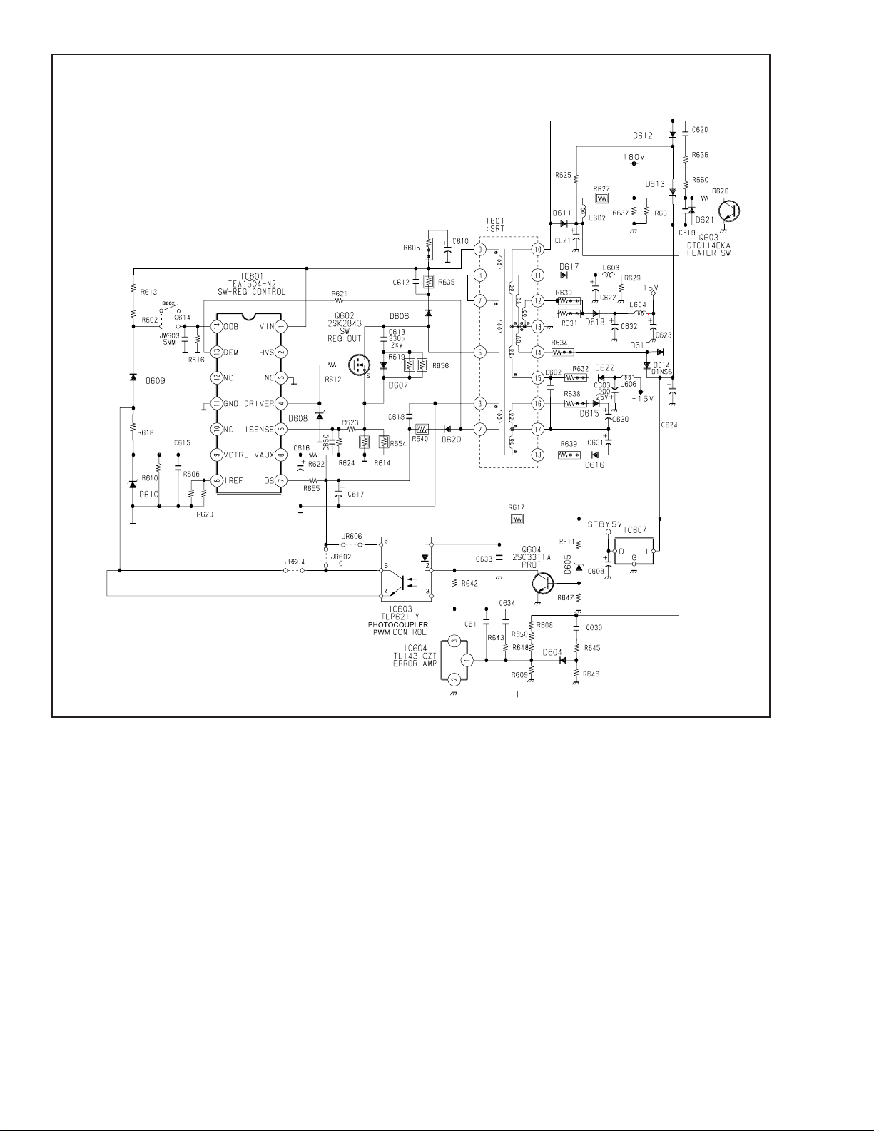
CIRCUIT DESCRIPTION
y
g
D BOARD POWER SUPPLY SECTION
Power Supply Electrical Circuit
The power supply is located on the D Board. It has three modes of operation that are controlled by a microprocessor. The
topology is a discontinuous mode flyback converter with photocoupler feedback for regulating the secondary voltages.
Circuit operation and troubleshooting are explained in the following sections:
Operation Modes Secondary Circuitry
AC Input Protection Cir cuits
Degauss Circuit T roubleshooting
Primary Circuitry
Operation Modes
The power supply has four modes of operation, ‘off’, ‘active off’, ‘suspend/standby’ and ‘active on’. These modes are
related to power savings and are indicated by the front panel LED. Additional indications are failure diagnostics and aging
mode. The table below lists operation mode, condition and LED status.
Mode S ync s Conditio n LED
Off N/A Power Switch Off Off
Active Off No H and V Low Power, Heater Off Amber
Suspend/Standby No H or V Low Power, Heater On Amber 0. 5s<- ->Green 0.5s
Active On H and V Present Phase Locked, Normal Oper ation Gr een
Failure 1 NA HV or +B Fai lure Amber 0. 5s<- - > O ff 0. 5s
Failure 2 NA H Stop, V Stop, Therm al Fail ur e Amber 1. 5s<- ->Off 0.5s
Failure 3 NA ABL Failure Amber 0. 5s<- - > O ff 1.5s
Aging/Self Test No H and V Aging Raster or Test Pattern Green 0.5s<- ->Off 0.5s
Except for power switch off, all modes of operation are controlled by the microprocessor located on the D Board. The
failure modes are detected by the microprocessor and the power supply is forced into active off mode. These functions are
discussed later (Deflection).
With the AC cord attached to the monitor and connected to an AC source, the monitor will be off until the power switch is
turned on. When the power switch is turned on, the power supply starts and is in active off mode. The next step is active on
mode. The power saving modes are activated by the microprocessor based upon the presence of either H or V sync. If no
sync signals are present, the power supply is set to active off mode. If only horizontal sync is present the power supply
moves to suspend mode. If only vertical sync is present the power supply enters standby mode.
Power supply operation control signals are “Remote On/Off” and “Heater On/Off”. Remote On/Off is digital low for active
off and suspend/standby modes. Heater On/Off is digital low for active off mode. To enter active on mode, the microprocessor must set remote on/off to digital high. Heater on/off is also made digital high and the heater is turned on.
Output Off Active Off Suspend/Standb
Active O n
B+ 0V 13V 180V 180V
80V 0V 10V 77V 79V
+15V 0V 1V 14V +15V
-15V 0V -1V -14V -15V
+12V 0V 0V 0V +12V
5V 0V 0V 0V +5V
Heater 0V 0V 4.6V 6.3V
H. Centerin
0V +7V +10V
STB Y 5V 0V +5V +5V +5V
- 2 -
Page 3
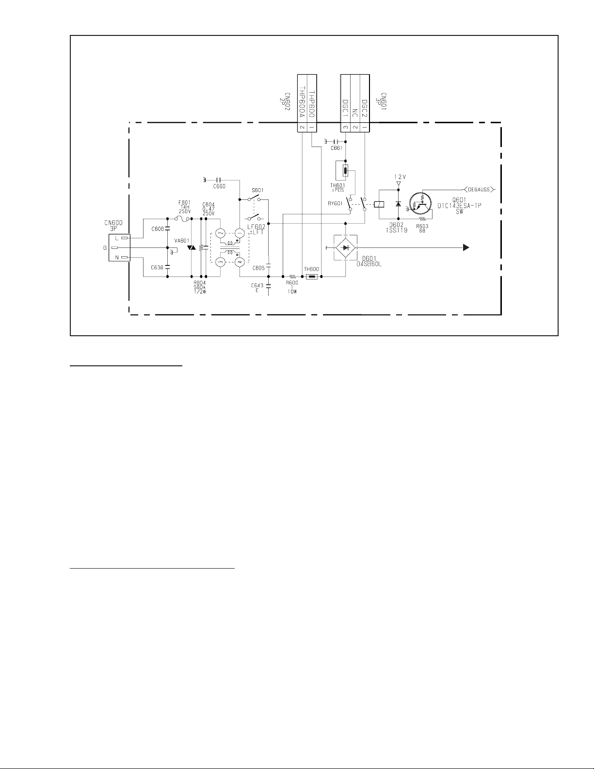
AC Input and Degauss
1. AC Input Section
The AC input section provides EMI filtering, input protection, surge limiting and CRT degauss operation.
EMI Filter
The EMI filter comprises CN600 (inlet with filter), X-capacitors C604 and C605, Y-capacitors C606, C638, C660 and
C643 and the line filter transformer, LF602. Input protection is provided by F601and VA601; surge current limiting by
thermistor TH600 and resistor R600. Degauss is explained in the next section.
Degauss Circuit
The degauss circuit is used to demagnetize the CRT. After power on, the microprocessor located on the D Board sets the
degauss signal to digital high and Q601 turns on relay RY601. This allows AC current into the degaussing coil through
posistor TH601. The current heats up the posistor and its affective resistance increases, this dampens the current in the
degauss coil to nearly zero. Duration time is approximately 5-6 seconds and the microprocessor then shuts off RY601,
which disconnects the degauss coil from the AC line. This operation should sufficiently demagnetize the CRT.
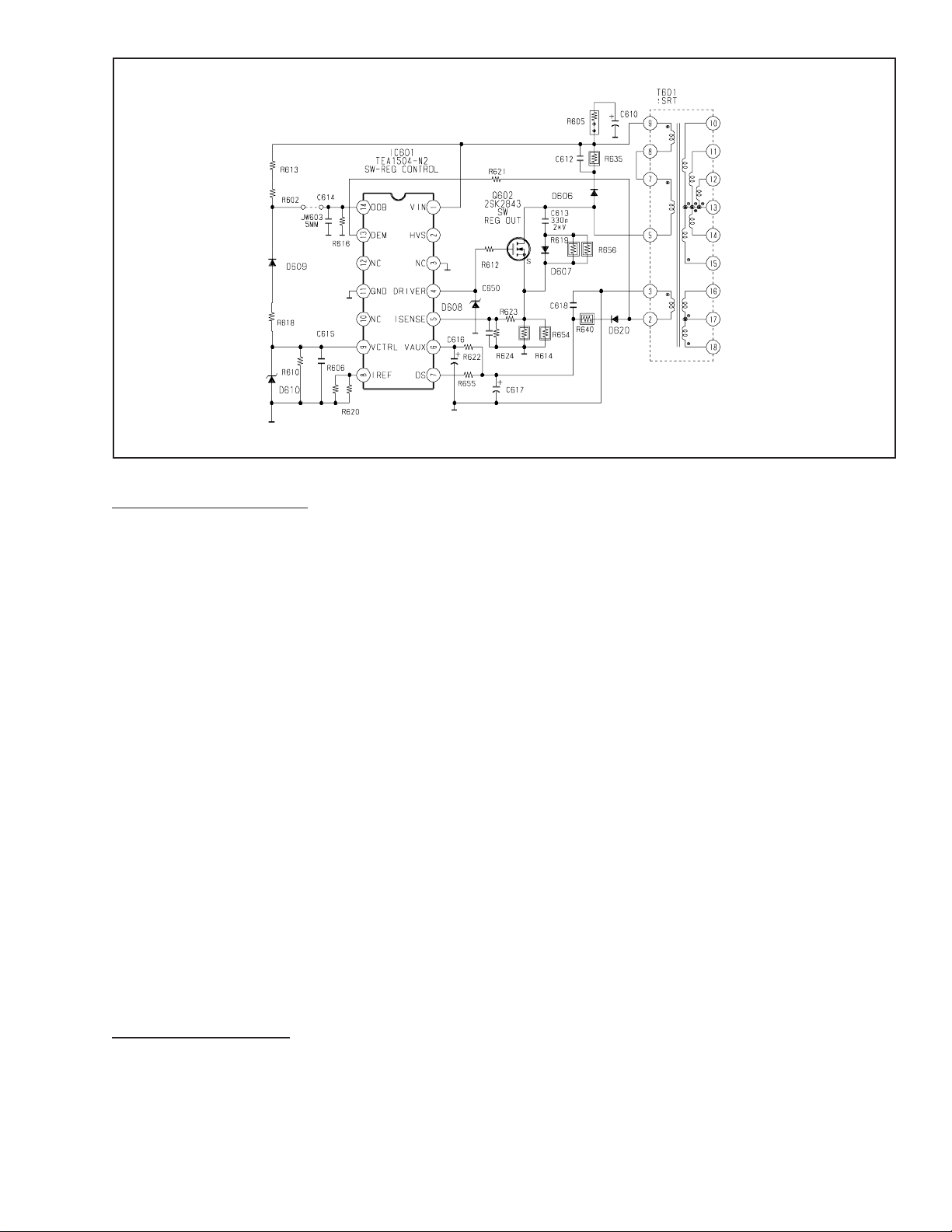
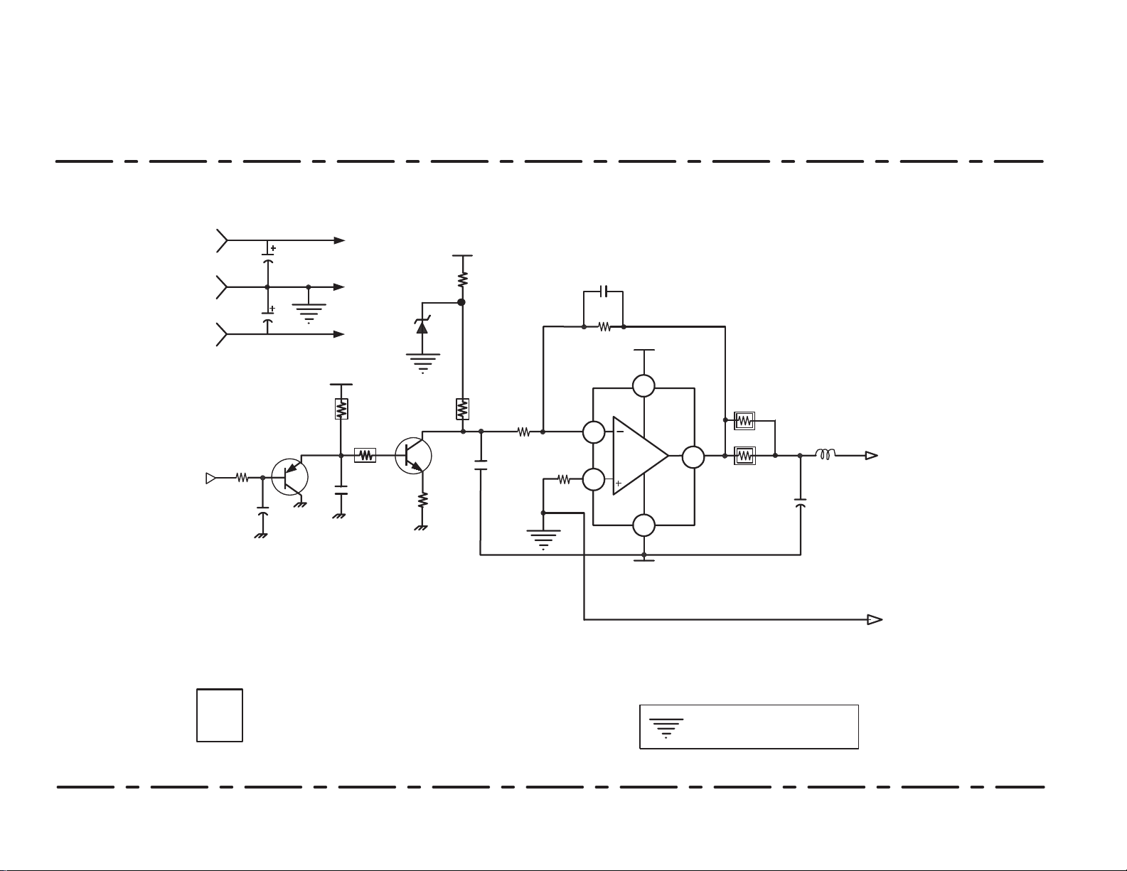
2. Primary Circuitry Section
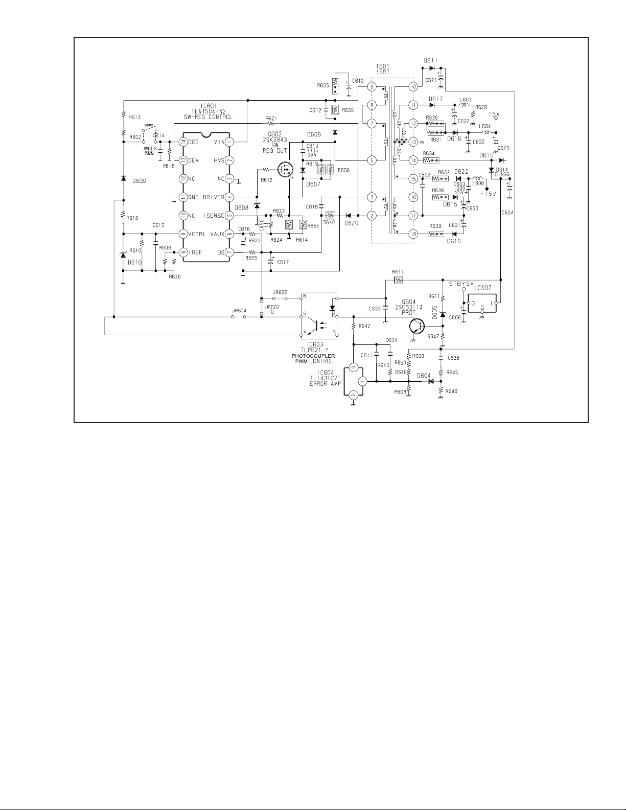
IC601
The heart of the primary section is the TEA1504/N2 power supply controller, IC601. The following describes the functions
of each pin.
Pin 1 – Vin: This is a MOSFET drain connection internal to IC601, which is connected directly to the DC mains v oltage rail.
The startup current source derives power from the DC mains via the Vin pin. It supplies current to charge the Vaux (IC
supply) capacitors C616 and C617 and also provides current to the IC601 control circuitry.
Pin 2 – HVS: High voltage safety spacer pin is a no connection.
Pin 3 – NC: Connected to primary side DC mains return.
- 3 -
Page 4

Pin 4 – Driver: Outputs the pulse width modulated gate drive for switching transistor Q602. Maximum duty cycle is set
internally at 80%.
Pin 5 – Isense: Provides cycle by cy cle over current protection by turning off pin 4 dr iv er output when Q602 current e xceeds
the current limit corresponding to 500mV at pin 5. This pin typically provides 425nS of leading edge blanking time. The
threshold voltage for switch over to low frequency (low power) operation is sensed by pin 5. When the voltage sensed at pin
5 is below 165mV, IC601 transitions from operating at high frequency (56.5KHz) to low frequency (23.5KHz).
Pin 6 – Vaux: IC601 supply pin. An internal current source from IC601 charges the Vaux capacitors C616 and C617 for
startup. Once the Vaux capacitors are charged to the startup voltage level (11V), then IC601 starts switching pin 4 driver
output. The Vaux is also supplied by an auxiliary winding from T601 on the primary side once the secondary output voltages
attain their nominal operating voltage values. Pin 6 also provides under voltage lockout detection (8V) and over voltage
protection (14.7V).
Pin 7 – DS: Provides the power supply for the driver output (pin 4).
Pin 8 – Iref: Controls IC601 internal bias currents, which determines the pulse width modulated switching frequencies.
High frequency is 56.5KHz during active on mode. Low frequency is 23.5KHz during suspend/standby mode.
Pin 9 – Vctrl: Feedback voltage for duty cycle control.
Pin 10 – NC: No connection.
Pin 11 – Gnd: Connected to primary side DC mains return.
Pin 12 – NC: No connection.
Pin 13 – Dem: Guarantees discontinuous conduction mode operation for the power supply. Verifies that T601 is demagne-
tized by not activating the next gate drive pulse until the primary side auxiliary winding of T601 is lower than the threshold
level of 65mV as detected at pin 13.
Pin 14 – OOB: On/Off/Burst mode input signal. A voltage greater than 2.5V enables IC601.
Operation
The power supply is a discontinuous-mode flyback converter with photocoupler feedback for regulating the secondary
voltages. The PWM controls the pulse width of the gate drive.
When AC is applied to the power supply and IC601 pin 14 is greater than 2.5V, start up current is supplied though IC601 pin
1 to IC601 pin 6. Startup voltage is approximately 11V. After start up, the voltage to pin 6 and pin 7 of IC601 is supplied
through D620 connected to T601 pin 2. The first mode of operation is acti v e off mode. The output drive pulse frequenc y will
be in burst mode operation.
When the power supply enters active on mode, the switching frequency will be 56.5KHz. The Vaux level will be approximately 12.5 volts. O VP threshold is 14.7 volts and UVLO is 8.0 v olts. T herefore, if the Vaux voltage is not correct, the powe r
supply will not operate properly.
Feedback from the secondary side comes through IC603 and IC604, which is connected to IC601 pin 9. (See diagram on
page 5.)
3. Secondary Circuitry Section
The secondary section consists of the following circuits. Rectifier diodes and filters for all output voltages, horizontal
centering, +5/12 volt regulators, +5 standby regulator, heater voltage regulator, voltage feedback circuit, active off mode
feedback, and protection circuits. This section will describe each circuit and its function.
Secondary Rectifiers
The secondary rectifiers supply the following voltages, 180V (B+) deflection and video, 80V video, ±15V deflection and
regulators, 6.3 volt heater regulator, +5V standby regulator, horizontal centering voltages.
- 4 -
Page 5
Horizontal Centering
This circuit supplies IC503, which is used to adjust horizontal raster position on the CRT. The horizontal centering circuit
consists of fusible resistors R638 and R639, diodes D615 and D616 and filter capacitors C630 and C631. In respect to the
secondary ground, the horizontal centering ground is floating and connected to –H DY line. T he voltages in reference to this
floating ground are ±10 volts. Care should be taken to not short the floating ground to the secondary ground.
+5/12 V olt Regulator
IC605 is the 12 volt regulator and IC608 is the 5 volt regulator. The output voltages are supplied to the microprocessor,
deflection and video circuits. The +15 volt line provides the input voltage for +12V regulator; the +12V line provides the
input voltage for +5V regulator. During active off or suspend/standby mode, the 12 v olt regulator is disabled via remote on/
off and subsequently the 5V regulator is disabled.
+5V Standby Circuit
IC607 is the standby 5V regulator. In the acti v e on mode and the suspend/standby mode, the input to the regulator is supplied
from T601 winding 14-13. During the activ e off mode, the regula tor input is supplied from T601 winding 10-13 via D612 and
D613. T ypical input v oltages to the re gulator are acti ve on mode: 9.5V; suspend/standby mode: 7.4V ; acti v e of f mode: 11.5V.
Heater V oltage Regulator
Heater filament voltage is supplied by T601 winding 14-13 and is regulated by IC602. IC602 output is turned on and off by
the heater on/off control line at pin 1, CTL. The output is off during active off mode.
Feedback Circuit
The feed back circuit is divided into two sections. One is for active on and suspend/standby modes; the other for active
off mode. The following two sections explains the theory and operation.
Acti ve On and Suspend/Standby Mode Feedback
Shunt regulator IC604 regulates the B+ line to 179.2V by sinking current through the opto coupler 1C603 to ground. The
- 5 -
Page 6
Feedback Circuits
reference voltage at IC604 pin 1 determines the sink current into pin 3. The reference voltage is set to 2.50 volts by
resistor divider R608, R650, R648, and R609. Since the B+ is connected to the resistor divider, any change in B+ voltage
is detected at the reference terminal. The shunt regulator will either increase or decrease the current into pin 3 in order to
decrease or increase the B+ voltage respectively and try to maintain the reference voltage to 2.50 volts. IC603 biases it's
phototransistor accordingly and drives IC601 pin 9 (Vctrl) which changes the duty cycle at IC601 pin 4 (driver) to
regulate the B+ voltage at 179.2V.
Active Off Mode Feedback
Heater control line is low (heater off) during active off mode and respectively Q603 is off. Voltage pulses from T601 pin 10
flow through C620, R636, and R660 triggering the gate of thyristor D613. D613 turns on effectively shorting the B+ rail to
the standby 5V regulator input; current flows from T601 pin 10 through D612 and D613 to the standby 5V regulator input.
When the standby 5V regulator input is increased to approximately 12.7V it forward biases zener diode D605 turning on
Q604 and sinks current through IC603 to ground. The standby 5V input supplies this current to IC603 pin 1. IC603 biases it's
phototransistor and drives current through D609 into IC601 pin 14 (OOB) triggering burst mode operation. IC601 pin 4
(driver) is pulled low turning of f switching transistor Q602. T601 pin 2 (auxiliary winding) feedback pulses are discontinued
and IC601 pin 6 (Vaux) decreases to 8V. IC601 internal current source then charges pin 6 (Vaux) to the startup voltage level
(11V) which starts switching pin 4 driver output. The feedback cycle is then repeated. The burst repetition rate is approximately every 110mS and when IC601 pin 4 is switching its frequency is 23.5KHz.
- 6 -
Page 7
4. Protection Circuits
Protection Circuits
The following are protection circuits: OCP, OVP, UVLO and secondary short circuits. OCP is pulse by pulse and is performed
on the primary side. OVP detects excessive output voltages. UVLO detects output under voltages. The following will explain
the operation of these functions.
OCP
OCP is activated if there is too much current passing through the po wer MOSFET, Q602. This condition will occur if either
the B+ line or 80 volt line is shorted.
R614 and R654 are the current sense resistors. Current through these resistors will produce a positive voltage reference to
ground. R623, R624 and C650 provide a voltage divider and filter to IC601 pin 5 (Isense). If the voltage level exceeds 0.5
volts, the IC does pulse by pulse current limit and the output voltages are reduced. This condition can be audible and
characterized by a ‘chirping’ sound.
OVP and UVLO
The OVP and UVLO functions are detected by IC601 pin 6 (Vaux). Vaux is mornally 12.5V. In the event the regulation
control loop were to fail, the output voltages would either increase or decrease; then Vaux would increase or decrease
respectively via T601 transformer coupling . IC601 pin 6 will detect an O VP at 14.7V and UVLO at 8V turning of f the driver
output and initiating a low dissipation safe-restart mode.
Secondary Short Circuits
Safe operation during secondary short circuits is provided by the demag function of IC601 pin 13. Demag protection
decreases the switching frequency to a very low level, thereby reducing the input power level and providing safe operation. Demag also provides a soft start function during startup gradually increasing the switching frequency until fixed
frequency operation is attained.
5. Troubleshooting
Warning
Before attempting to fix the power supply, safety should be considered first. Never connect test probes to the primary side
circuits, unless proper isolation has been installed. If isolation for the AC mains is not present, serious harm can occur.
Never assume you are safe.
- 7 -
Page 8

No Power
In the event that the monitor does not turn on, first verify input power is applied to CN600 and the front panel power switch
is turned on; then check F601 and R605. If these parts are blown, the primary side circuitry should be checked. If the fuses
are not blown, then check the secondary side circuitry, especially the protection circuits. If these circuits are causing a no
power symptom, the problem can be more readily found.
AC Input and Degauss Cir cuit T r ouble Shooting
For no power or nonoperating power supply, the AC input circuitry should be checked. Open or short circuit elements will
cause non-operation. F601, CN600, and R605 on the D Board should be checked first. Check the front panel power switch
for continuity.
If all elements are correct, check whether F601 breaks when power is applied and the power switch is closed. If the fuse
does blow, there may be problems with the primary circuitry or a component short.
The degauss will malfunction if CN601 is not connected. One problem could be loss of degauss signal from the microprocessor. This can be verified by using the manual degauss command found in the OSD menu. If the signal does not appear at
Q601 base, then it is possible that the microprocessor does not function correctly or standby 5V is not functioning.
The second step is to place a short across the AC terminals of RY601 for less than two seconds. If degauss operates then
check Q601 and RY601. If degauss does not work, check TH601 for an open condition and VA600 for a short condition.
Primary Section
Three main areas can diagnose primary circuit failures. These are IC601, Q602 and Feedback system.
Visible checks of these areas will aid in finding problems. The following will discuss each section.
IC601
First apply AC to the monitor and check IC601 pin 4 output. If the output on pin 4 is not present, there could be problems
with Q602 and related parts or pin 14 could be less than 2.5 volts. Further, check Vaux level at pin 6. If it less than 11
volts, the IC could be in safe-restart mode. If the voltage is very low, there could be a short on any of the IC pins. In
reference to ground, check the impedance of pin 1, 8 and 14. If any of these pins are shorted, replace the IC and check
components connected to the related pins. Take care that C617 and C616 are fully discharged before replacing the IC.
Q602
The switching transistor can be damaged in various ways. These are related to voltage, current and temperature.
Check whether the transistor is shorted across drain and source terminals. If there is a short, F601, R605, R614, R654,
R623, R624 and C650 should be checked. Additional components to check are D608, R612 and IC601. If Q602 is
shorted, all these parts should be replaced.
Failure of a secondary rectifier diode can also cause Q602 to fail. Check 180V and 80V diodes for open or short conditions. There is also a clamp circuit, which is used to clip the turn off spike found on Q602 drain. If the clamp circuit is
broken, it can cause Q602 failures. Check D606, C612 and R635. Also check the snubber circuit components C613,
D607, R619 and R656.
Secondary Circuit
Failure in the secondary circuits can be categorized by rectifier diodes, fusible resistors, regulators, feedback loops and
protection circuits. These sections are interrelated and failure in one can affect another. Consequently, some failures will
also affect the primary circuitry.
Rectifier Section
Rectifier diode failures are not common, but do occur. Deflection, video and high voltage circuitry failures contribute to
diode damage. In the event a voltage is not present, check for shorts to ground, open or short diodes. Also check fusible
resistors found on the voltage lines.
Horizontal Centering
Loss of horizontal center adjustment can be affected by the rectifier diodes, fusible resistors, IC503 and related circuitry.
Measure the voltages in reference to the horizontal centering ground. Typically, the voltages are ±10 volts. However, the
adjustment setting can reduce the voltages. If there are no problems found with the diodes or fusible resistors, the next
step is to check the adjustment signal at Q506. If the adjustment signal is not present check the IC901 pin 4. Otherwise,
check IC503 and related components.
- 8 -
Page 9

+5/12 Volt Regulator
Loss of voltage due to shorts or device failures on either +12 or +5 volt output lines can occur. Consequently, IC605
or IC608 can be damaged and need replacing. Before replacing either IC, check for shorts or damaged parts along the
output lines. If +12 volt does not appear, check the remote on/off signal from IC901 pin 6.
Standby 5V Circuit
Failure of this circuit can be affected by IC607. In case the circuit does not work properly, check D605, D614, R634,
R611 and Q604. If these components are good, check the remaining circuit parts.
Heater V oltage Regulator
This circuit may be affected by fusible resistor R634 or D619. If these parts are good, check the regulator output for a
short to ground. Shorts can occur on the video board. In the case of an output short, IC602 may have been damaged.
If the IC appears to have no damage, check for any problems with the heater on/off signal.
Feedback Cir cuit
Problems with feed back can cause power supply shut down or low voltages. First determine whether the power
supply is operating in active off, active on modes or not at all.
The power supply can be stuck in active off mode. The remote on/off signal, Q603, Q604, D605 and IC603 can affect
this condition. Likewise, if the power supply is always in active on mode, the same items should be checked.
Checking for voltages at IC603 pins 1 and 2, IC604 pins 1 and 3 can solve more difficult problems. Additionally,
IC603 pins 4 and 5, and IC601 pin 9 should be checked. If there are problems with these devices, 180V or standby
5V line, the feedback systems will not work correctly. Also check the protection circuits.
Protection Circuits
OCP occurs when there is excessive current through Q602. Failures with Q510, Q507 or the video section could
cause this condition. These areas should be checked. OCP condition can also occur if R614 or R654 are open; if
R623 is shorted; or if R624 is open.
OVP usually occurs when the feedback loop is open, or loss of standby 5V. Isolate the OVP trigger condition, by first
checking the operation of the feedback loop.
D BOARD DEFLECTION SECTION
1. Horizontal Deflection Circuit
Overview
These circuit drive the DY (Deflection Yoke) for Horizontal Deflection. The H size and H shape control (IC501 and
around) is included in this page as well.
H Drive, H Out, Feedback
+12Vp-p HD pulse is generated by the inverter Q903 using the Jungle IC902 H. out pin #17. And switch Q511
through A push-pull amplifier (Q501 and Q502) buffers. The drive current which introduced in HDT (T504) by this
switching will drive Q507 (H out Tr) and 1000V pulse appears on collector. D506 is the "Damper Diode" which avoid
the negative pulse and discharge the energy for next Horizontal Drive. Q508 is the buffer for the "H BLK" feed back
to Jungle IC 902 H. FLY pin #14 and it will be the reference of phase / jitter control of Jungle. HST (T505) is to sense
the deflection current through DY. The voltage appeared on secondary side will be the feed back for H Size/Shape
control.
H Size/Shape control
HD pulse also triggering the H Size/Shape control IC501 pin #8. IC501 is "PWM IC" and it controls H and HV B+
chopper duty. H Shape and H size information is already included and coming from Jungle IC902 E/W pin #9. It will
be supplied to IC501 pin #2. H reg output pin #20 is switching pulse of Q520 (B+ chopper). The energy supplement
from 180V to H Def circuit (through L503 HOT) is controlled by the duty of this pulse. The H Shape input and
feedback voltage from T505 are compared by error amp (in IC501) and H Reg out pulse duty is controlled to keep the
level of these two the same.
- 9 -
Page 10
C543
H Deflection Circuit
C563
R551
R553
320
H DefINH Reg
Out
PWM IC501
E/W PIN #9
IC902
FB506
R581
180V
C575
12V
TO:
H Lin and
Ringing Circuit
1
H SHAPEINHD
R569
28
C582
IN
R586
R582
R583
- 10 -
C574
C576
T504 HDT
D518
D516
FB504
Q520
B+CHOP
2
5
L503
Q518
3
4
3
2
T504
HST
HDYHDY-
HOC
CN801
HD output pin #17
IC902
R933
Q903
12V
R594
R506
Q501
Q502
12V
C502
R508
R508
D501
Q511
1
4
D502
R513
C510
8
6
2
1
2
1
H DY+
H DY+
H BLK
R517
R518
Q507
H-OUT
D506
C518
C521
C522
Q508
TO IC901 #32 pin
IC902 #14 pin
R511
-16V
Page 11

Troubleshooting
See attached “FLOW CHART” and confirm if it’s really H Deflection issue.
No H Deflection / No Power
Check Q507, Q520 and D506 first. In case any of these shorted, check T504, Q511, R511 and D502.
Those parts might have been damaged.
If both of Q507, 520 were not broken, check the HD pulse at the gate of Q511.
If no pulse, check Q501, Q502, Q903.
Otherwise, check R582, D518 or try changing IC501.
Bad Distortion
Check pin#2 of IC501 and confirm that proper DC level and AC waveform.
If the distortion is on only right side, check all above (“No H Deflection”).
Otherwise, refer to the Troubleshooting of next section (“H Lin and Ringing Correction”).
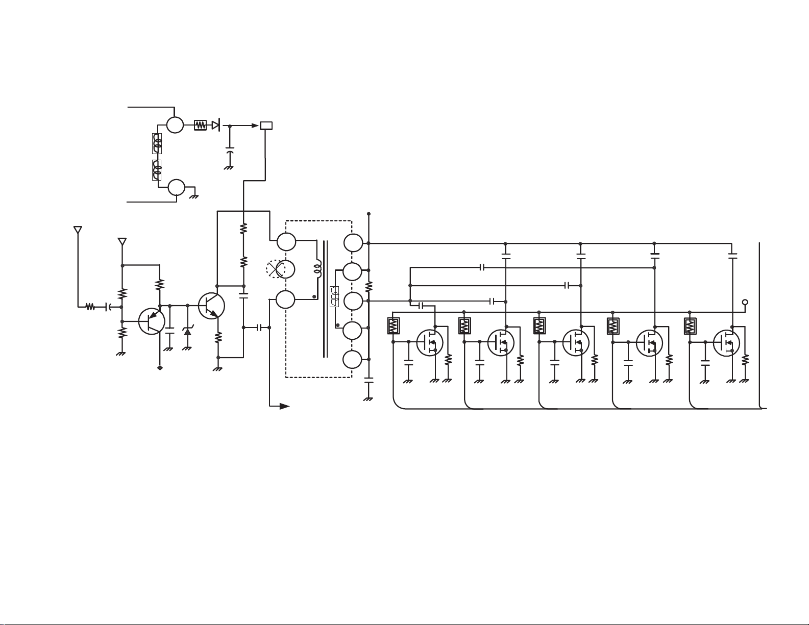
2. H Linearity and Raster/Distortion Ringing Correction Circuit
This section includes HLC Control circuit, S cap switching and HLC/S-Cap Damping circuits. These circuits are placed
directly on the “cool side” of DY which is in series with deflection current line.
H Centering circuit will be explained in next section.
HLC Switch Control and HLC Damping
There is HLC switch circuit. In case that Q519 is on, RY500 turn on then, L509 is shorted. Q519 is controlled by Microprocessor (IC901). D505, R577 and C581 are damping circuit to avoid the raster Ringing (mainly on left side of picture)
caused by HLC, DY and S-caps.
S-Cap switching and S-cap Damping
H Def current is distorted by resonance between S-Cap and DY to correct the linearity. Since the resonance frequency has
to be changed for each fH, S-Cap switching is controlled b y MICRO
S-Cap Switch - FETs (Q512, Q513, Q514, Q515, Q516) are "On" when its gate is Hi(5V) and that moment, drain voltage
should be grounded (0V).
L506, R578 and C573 is damping circuit to avoid Distortion Ringing (mainly on top of the picture) caused by S-caps and
H Control loop gain. L505, R575 and C572 is also the same purpose as above but only works when Q519 (Switch for the
Biggest S-Cap) is “On”.
Troubleshooting
See attached “FLOW CHART” and confirm if it’s really H lin issue.
Bad Linearity
Confirm that Raster is approximately in the center of the Bezel. If not, refer to next section (Raster Centering Circuit).
Check S-cap switches (Q512, 513, 514, 515, 516, HLC switch (Q519)) and confirm that H Linearity changes proportional
to the value of “S-Cap”.
Bad Top Distortion/ Left side Raster Ringing
Check damping circuits explained above.
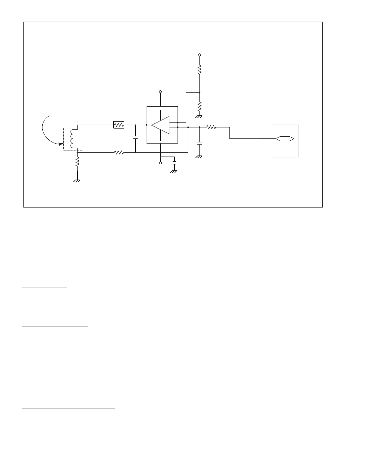
3. H. Raster Centering Circuit
Overview
H Centering is changed by supplying DC current to DY. D99 is taking the common level on DY cool(-) side and +/- 8V from
power supply transformer(T601 PIN#16, 17, 18. #17 is the common).
H Center Circuit
The DC current is outputted by powered OP-amp (IC503). This circuit is making “invert amp” with the gain of R573/R579
and input 1S Q518 collector. The level is controlled by MICRO”H CENT" pin #4 through Q506(buffer).
- 11 -
Page 12
CN501
HDY - #5.6 pin
R593
#
L508
HLC
H SIZE/Shape Feedback
12V
3
2
R592
150
1/2W
:RN
4
5
1SS119
R577
33
3w
D512
T505
1
C517
0.01
:PT
R590
22k
:RN
R589
4.7k
2SA1309A
:DFT
T503
Q521
L509
HLC
C583
0.1
:PT
+
C573
4.7
250V
RY500
R578
39
2W
:RS
#
TH502
R591
150
1/2W
R516
:RN
150
1/2W
:RN
C581
#
- 12 -
D505
ERB91-02TP1
5
C511
0.22
R512
4.7
250V
:PP
4
3
R515
1k
:FPRD
2
C507
1
0.19
400V
C512
0.01
B:CHIP
S4
L506
820µH
R521
:FPRD
S
Q514
2SK3332
1k
R519
56k
:RN
R576
47k
12V
1SS119
C514
0.82
250V
C530
250V
S3
D519
:PP
0.12
C568
0.047
400V
:PP
C515
0.01
B:CHIP
Q519
DTC114TSA
C572
+
4.7
250V
R575
68
1/2W
:FPRD
L505
2.2mH
S
C516
250V
R525
1k
:FPRD
R524
56k
:RN
0.3
:PP
250V:PP
2SK2098
S2
H CENTERING CIRCUIT
C523
0.12
250V
C531
0.068
Q513
C520
0.01
B:CHIP
Q512
2SK3332
R533
:FPRD
S
1k
R523
56k
:RN
Q515
2SK3332
S1
C536
0.01
B:CHIP
S
C525
0.047
400V
:PP
R536
1k
:FPRD
R535
56k
:RN
S0
Q516
2SK3332
C538
B:CHIP
0.01
C529
0.047
400V
STBY
5V
S
:PP
R537
56k
:RN
S4
D
(BOARD)
H. LINEARITY AND RASTER/DISTORTION RINGING CORRECTION CIRCUIT
Page 13
FROM D615 IN P.S.
C670
HC+
HC+
C580
R579
2
1
HC+
5
3
HC-
IC502
R538
L510
4
R539
C570
TO H. DY(-) VIA L503
(DRAIN OF Q520)
TO H. DY(-) VIA L510
Q518
R580
R570
D511
R571
C559
R573
R572
FROM PIN #17 T601
FROM D616 IN A.S.
- 13 -
H CENT
C506
C631
R514
R529
Q506
HC N
HC-
T120
R500
C509
D
(BOARD)
(19D99 H. CENTERING CIRCUIT)
!!! IMPORTANT !!!
COMMON (ISOLATED)
=
CENTER VOLTAGE
Page 14
#1, 2 PIN
Rotation Coil (CN701)
R563
R562
Rotation/Vertical Key Circuit
STBY
5V
+15V
IC502
C549
5
V+
3
1
+
V-
-
2
4
R558
R559
R560
ROTATION
3
C547
IC901
R566
-15V
C513
Trouble Shooting
See attached “FLOW CHART” and confirm if it’s really H Center Circuit issue.
No Raster Centering Control
Check R638, 639 (Right next the SRT) first. If it’s open, change IC503.
Confirm that voltage of Q5l8 base is changing accordingly to “HCENT _MINFH, HCENT_LO_FBFH,
HCENT_HI_FBFH, HCENT_MAXFH” register.
If not, change Q506.
CAUTION!!
The heatsink of IC503 is connected to the H center(-) level, not GND! It could have up to 150V and should not be
touched to any other metals.
4. Rotation Circuit
Rotation is a PWM waveform at approximately 125kHz measuring 5Vp-p at pin #3 of the micorprocessor IC901. Then
filtered by R560 and C547 combination. The DC current is outputted by powered 0P-amp (IC502). The output current from
pin #4 of IC502 flows through R563 and the rotation coil and returns to ground through R566. The feedback is sensed at
R566 and sent back to the amplifier through R562.
No Rotation Control
Check the waveform pin #3 of microprocessor IC901 if it is 5Vp-p PWM and approximately 125kHz. Otherwise, check
around IC502.
5. Dynamic Focus Circuit
Overview
Both H and V Dynamic F ocus are combined through DFT (T503).
- 14 -
Page 15

H DF
Horizontal Parabola is injected into the secondary side of the focus transformer (DFT:T503). In order to keep the amount of
parabola constant over the horizontal frequency range the values of the AC coupling capacitors are changed by the transistors, which switch the s-caps. This signal is amplified by the turns-ratio to the primary side of the transformer.
V DF
V DF waveform is buffered by Q505 and amplified by Q504 to about 150vp-p. VDF is controlled by Jungle IC902 pin #12.
300v Vcc is made by FBT through D515. This voltage is also used for HV Protector.
Troubleshooting
See attached “FLOW CHART” and confirm if it is really a DF issue.
Bad H DF
Check H. Linearity. If it's no problem, change T701, T503 (DFT).
Bad V DF
Confirm that waveform is around 1Vp-p. If it’s more than 2.0Vp-p, change Jungle IC902.
Check 300v from FBT from Jungle pin 12 IC902.
6. High Voltage Pr otect Circuit
This circuit generates the High Voltage supply for the anode and G2 (1000V) of the CRT. It consists of a high voltage driver
and regulator similar to a switching power supply function. In addition, there are High Voltage and Beam Current protection
circuits. All those circuits are similar to D1 chassis circuits.
High Voltage Regulation and Output Circuit
The HV Drive pulse is generated by IC501 and synchronized with Horizontal drive pulse. It is supplied to the Gate of Q510
the HV Out FET .
The HV Out Pulse approximately 700V, is generated by Q510 switching with the peak voltage being controlled by the
switching duty of Q503 (B+ chopper). Internal resistors and R540 and RV501 divide HV generated in the FBT. Since this
voltage is the feedback for HV Regulation control. Adjusting RV501 will result in changing the HV Regulation level(= HV
level). HV Feedback voltage is returned to IC501 at pin#12 to be compared with an internal reference voltage of IC501 at
pin#13. According to this feedback level, IC501 changes the pulse duty cycle. This pulse is felt at pin #18 of IC501 thereby
controlling the output of B+ chopper drive Q503.
G2 V oltage
G2 voltage at approximately 1250vdc is produced by the HV Out Pulse rectifying through D510, C528, D520, D521, C578
and C577. This voltage will be supplied to A board via CN 510, which contains the G2 control circuit.
HV Protect Cir cuit
HV Protect circuit will be activated by the Microprocessor when the signal at HV DET, Microprocessor pins#18 reaches a
+5vdc level. HV DET indicates the level of the primary current developed by the 300V winding of the FBT through R543,
D515.
Beam Current Protect
Beam Current Protect will be activated when ABL DET at microprocessor pin#16 reaches a level of 0V when operating in
main mode. ABL DET level is corresponding to the Beam Current which is supplied to FBT through R596, R550 and R548.
The voltage current relationship is inversely proportional Voltage (down) Current (up).
T roubleshooting Hints
See attached FLOW CHART to confirm if is really an HV/Protect Circuit issue.
No HV / No Power
Perform basic checks of Q510 and Q503 first. If both Q510 and Q503 were not broken, check the HV Drive pulse at the gate
of Q503. If no pulse, check R534 and D509. Otherwise, check R520, D504 or try changing IC501.
No G2 Voltage
Check R532 and D510, D520 and D521.
- 15 -
Page 16
Dynamic Focus Circuit
FBT
R543
D515
7
FBT
C540
6
:DFT
TO FBT
PIN #15
T503
R519
56k
:RN
C568
0.047
400V
:PP
C530
0.12
250V
C515
0.01
B:CHIP
S3
C516
0.3
250V
:PP
R525
1k
:FPRD
S
R524
56k
:RN
2SK2098
S2
C531
0.068
250V
:PP
C520
0.01
B:CHIP
C523
0.12
250V
2SK3332Q513
S
Q512
R533
1k
:FPRD
R523
56k
:RN
C509
100p
500V
B
S1
Q506
2SA1309A
Q515
2SK3332
C536
0.01
B:CHIP
S
C525
0.047
400V
:PP
R536
1k
:FPRD
R535
56k
:RN
S0
Q516
2SK3332
C538
B:CHIP
0.01
C529
0.047
400V
STBY
5V
S
:PP
R537
56k
:RN
S4
5
C511
0.22
R512
4.7
250V
:PP
4
3
C512
0.01
R521
:FPRD
S
Q514
2SK3332
1k
R515
1k
:FPRD
2
C507
1
0.19
400V
B:CHIP
S4
VDF PIN #12
IC902
12V
R502
180k
:RN-CP
- 16 -
+
C501
R501
10
100
R503
CHIP
10k
:RN-CP
Q505
2SA1309A
R505
10k
C503
0.01
-15V
B:CHIP
D529
MTZJ-T-77-18
Q504
2SC3941A-QR
R506
330k
:RN
R507
2.7k
:RN
R565
330k
:RN
C504
330p
500V
B
C505
15pF
2kV
6
7
8
Page 17

Protect Malfunction
To see if HV Prot or ABL Prot are suspect check the Shutdown Log data at the Shutdown Log register. Refer to Shutdown
Log Table below.
When an HV Shutdown is indicated, check R917, R921 and D905 or, replace T501 (FBT).
Where ABL Shutdown is indicated, check the voltage T901 pin#11.
If it is higher than 0.5v immediately prior to shutdown, check connections all the way to N board. Should the voltage reach
and remain at the 0 volt level, even after the first 2.0 seconds of Power On, check D909 and 904 or check White Balance.
SHUTDOWN LOG TABLE
Bit Register value Shutdown Mode Comment
bit7 128 N/A N/A
bit6 64 N/A N/A
bit5 32 Thermal Explained later
bit4 16 ABL Shutdown Hardware Controlled
bit3 8 HV Ove r Hardware Controlled
bit2 4 HV U Shutdown Not Used
bit1 2 No Vertical Scan Explained later
bit0 1 No H Scan Explained later
7. Protection Circuitry Overview
Overview
The D99 chassis was developed with protection circuits other than HV/ABL.These protection circuits are controlled by
Microprocessor (IC901);
- Thermal Shutdown: Activates when S-Cap Switch in FET are broken (especially Q513 and Q514).
- V Scan Shutdown: Activates when Ver tical Deflection signal is absent or of insufficient level or of a distorted nature.
- H Scan Shutdown: Activates when Horizontal Deflection signal is absent or of insufficient level or of a distorted nature.
T roubleshooting Hints
S Cap Switch Shutdown
In the event of failure of any S-Cap Switching FETs, the Microprocessor detects temperature of FETs (Q513 and Q514) by
TH501 and goes into shutdown mode. For these conditions, refer to the section of H Linearity Circuit.
V ertical Scan Shutdown
If the V FLY feedback at pin #19 the Microprocessor doesn't get pulse around 1.5 second, a Shutdown will be initiated.
Power Supply problems may also produce a similar type failure. For these conditions, refer to the V Deflection Circuit or
the Power Supply section.
Horizontal Scan Shutdown
If the H BLK feedback at pin #32 of the Microprocessor doesn't get pulse around 500mSec, Shutdown will be initiated.
Some power Supply problems may also produce a similar type failure. For these conditions, refer to the H Deflection
Circuit or Power Supply sections.
8. Vertical Deflection Cir cuit
Theory of Operation
The negative input of amplifier IC401 is driven by VSAW signal generated by Jungle IC902 pin #8. The positive input of the
amplifier is Vref Signal generated by IC701 (Convergence IC) pin #5. VSAW is centered on 5. 0V, and sawtooth waveform
that controls VSIZE. Vref is a reference that is compared to VSAW at IC401. VCENTER is controlled by the shift of VSAW.
IC401 serves as a transconductance amplifier (it amplifies a low level voltage into a high level current) for VSAW and the
DC difference between VSAW and Vref. The current gnerated by IC401 is feed to the Vertical Deflection Coil. At the return
point of the Vertical Deflection Coil the current flows through R403 and R405 which generates a voltage across them which
is feed back to the amplifier via R404.
V FLY is generated by flyback pulse generated at pin 3 of IC401. If the flyback generation at IC401 does not work, then the
- 17 -
Page 18

HV REG DRIVE
PIN # 18 IC501
R534 C527
D509
R527
180V
B+ CHOPPER HV
S
D513
FB502
Q503
R561
R530
R531
C526
L501
L502
T501
:FBT
- 18 -
2
HV DRIVE PIN # 19
IC501
R520
R574
D520
CN510
G2 1ku
C577
D521
HV DET PIN # 18
D517
IC901
C544
R552
D
BOARD
19 D99 CHASSIS HV/PROTECTOR CIRCUIT
D504
C542
Q510
HV OUT
C578
C528
R595
S
D510
R549
R510
R547
300V
C519
R532
D515
C540
R543
1
5
7
9
10
7
6
HV
13
16
FV1
15
14
FV2
11
12
ANODE OF CRT
R597 R541 R568
C534
R542
R540
RV501
C532
CRT VIA
RED FV LEAD
H DF OUT
SG501
H&VDF OUT
CRT VIA
BLK FV
LEAD
D514
C535
R545
R546
C539
R544
R548 R550
ABL DET PIN #1
C556
R596
C541
IC501 PIN #12
"HV FEEDBACK"
12V
R934
ABL DET PIN #16
IC901
C928
Page 19

IC401
C403 D401
3
62
+15V
+16V
C404
Flyback Generator
0
9
+
V+
V-
-
RL
TDA8177
LVDY
5417
R401 C402
- 19 -
V-DY through CN501
C409 R409
R410
5
Vref
IC 701
(CONV)
IC 902
R406
8
VSAW
(Jungle)
R404
-15V
C401
0
C406
D-BOARD
R402
R405R403
0
Page 20

Front Input
2
C Communication
I
V Sync and H fly
Heater and Focus Voltages
from D Board
Video
Process
D/A Conv
RGB Cathode Drv
D/A Level
Cuttoff
Voltage
J001
CRT
G2 V oltage
OSD Generation
G2,Cutoff
17 D99 Chassis A
Board Block Diagram
monitor goes to be shutdown as a V scan failure by microprocessor after wait around 1.5sec w/o VFLY.
Troubleshooting Hints
Vertical Scan Failure
The first step is to check the shutdown log of the monitor and make sure the microprocessor has detected a loss of VFLY.
Once this has been verified the output of IC401 should be checked. If a normal output exists after the remote on/off bit is
turned on but the monitor still shuts down then the VFB detection circuit is malfunctioning. If no output exists signal
tracing should begin at IC902 pin #8 (VSAW) and IC701 pin 5 (Vref). In shutdown mode both of these levels should be
5.0V DC. If the remote on/off bit is turned on a sawtooth waveform of about 1Vpk-pk should appear on VSAWN while
DCC2 stays at 5.0V this should last about 1.5 seconds until a loss of VFLY is detected and the monitor shuts down again.
If the signals make it this far, the problem is likely in the IC401 area.
VIDEO "A" BOARD ELECTRICAL CIRCUIT
The Main function of the A Board is to receive incoming video signals and then process them into the RGB video drives
necessary for proper CRT biasing. The input signals (RGB, Separate & Composite Syncs and DDC) are received with the
conventional 15 D-sub connector. The RGB signals (0.7Vpp) are sent to the preamplifier (IC001) where they are amplified
with Contrast gain and Brightness offset. Next they are sent to the Video Driver for final amplication to drive the cathodes.
The Horizontal Sync pulse is buffered and then sent to the Microprocessor along with the Vertical Sync pulse. DDC is no
longer handled on the A Board. It passes through the A board directly to the micorprocessor.
IC003 is the On Screen Display (OSD) generator. OSD mixing is performed in IC001. Additional functionalities of the A
Board include processing of all the CRT cathodes operating voltages; heater, G2 control, cathode DC bias, and focus.
- Sync Timing Buffering.
- RGB video signal amplification and adjustment according to white balance requirements, contrast and
brightness settings.
- On Screen Display mixing.
- D/A conversion for RGB CRT cathode cutoff G2 levels control.
- 20 -
Page 21

Video Input (0.7Vpp)
Video Select and RGB Process Functions
+12V
+5V
IC001
8
22
20
24
27
D/A
Cutoff
Control
3
4
5
6
D/A G2 Control
R
G
B
R
G
B
Board
From N
From IC003
R
G
B
2
I
C Data
2
C CLK
I
CBLK
BPCLP
R_OSD
B_OSD
B_OSD
OSD_BLK
11
9
7
1
2
18
12
15
14
13
17
+12V
3
4
5
2
+12V
10
8
9
11
IC004
IC003
+80V
6
D104
C206
R
G
B
C106
CRT
D106
D206
D306
5
3
1
C306
D105
0
+B
11
10
7
8
9
13
1. RGB Signal Processing (A Board)
RGB Signal Amplifiers
RGB video signals are amplified by IC001. Here the individual Sub Contrasts, Brightness offsets, and Contrast gain levels
are set by the Microprocessor via I2 C control. The OSD RGB video signals from IC003 are mixed into the main video
channels inside IC001. IC002 provides a final amplifier stage for the RGB video signals. This video driver is internally set
to a gain of –14. Therefore at the output pins of IC002 (Pin1, 3 & 5) the waveform is inverted with typical drives levels on
the order of 45Vpp. The Video Driver IC002 drives the CRT cathodes via AC coupling.
RGB Cathode Cutoff Amplifiers
The Red cathode DC cutoff level is amplified by IC004. It is controlled by the D/A output of IC001. The Red cutoff level is
clamped by discharging C106 via D106. The Green and Blue cathode Cutoff levels are clamped in a similar fashion. The
individual cathode cutoff levels are set for white balance by the Microprocessor via I2C communication with IC001.
T roubleshooting Hints
1) If the screen is blank with no output check:
- Video signals with proper cutoff levels are provided to the CRT cathodes.
- Supply voltages are at the appropriate levels and locations starting at CN305.
- Heater voltage is correct and present at the heater cathode.
- Diode shorts at the cathodes.
- Sync timing signals are present at the output of IC006.
- That there is I2C communication to IC001.
2) If the screen is lighted with no video check:
- Control, blanking and clamp signals to IC001, IC002.
- +5V, +12V, and +80V to these circuits.
-For shorted diodes on the IC002 outputs.
- 21 -
Page 22

Block Diagram IC003 OSD
SS
VFLB
VCO
HFLB
VDD(A)
VSS(A)
V
DD
V
SS
7
8
6
MCLK
VPOL
10
CHS
VERD
CH
3
RP
2
5
HPOL
4
1
16
BUS ARBITRATION
8
6
BACKGROUND
SDA(MOSI)
SCL(SCK)
DATA
RECEIVER
MBUS/SPI
RFG
LOGIC
NROW
VERTICAL
CONTROL
CIRCUIT
MCLK
HORIZONTAL
CONTROL
and PLL
WADDR
54
GENERATOR
DHOR
SC CCLK
8 DATA
9 ADR
9 ADDRC
32 Y
R4
7
HORD
W
WCOLOUR
and CONTROL
X32B
7
DISPLAY
MEMORY
CONTROL
REGISTERS
and DATA
MANAGEMENT
RDATA
4
LP
3
15
Z
32
8
ROW
BUFFER
CRADDR
CHARACTER ROMS
HIGH RESOLUTION FONT 12 X 18
CHAR
12 BITS SHIFT
REGISTERS
OSD_EN
LUMINANCE
COLOUR ENCODER
15 14 13 12 11
R
B
G
8
6
54
15
6
12
BLACKEDGE
INT
FBKG
HORD
VERD
CH
OSD_EN
SHADOW
BSEN
X32B
VPOL
HPOL
WADDR
WCOLOUR
and
CONTROL
13
CCOLOURS
and SELECT
CHS
CWS
CWS
BSEN
SHADOW
CCOLOURS
and SELECT
13
Block Diagram IC004 Cut-off Module
12 V
2
Vref
GND
1
Video signal (R)
+B voltage
11
3
R-Cont in
R-bias out
7
G
b
l
o
c
k
Similar to R block
CRT cathode (R)
B
b
l
o
c
k
- 22 -
Page 23

3) If colors are wrong or missing and white balance cannot be adjusted check:
- Each individual color signal path comparing DC offset and peak to peak signal levels to each other to determine if
there is any single amplifier at fault.
- For shorted diodes on the IC002 outputs.
2. On Screen Display Functions
On Screen Display(OSD)
IC003 is the On Screen Display character and graphic generator. It provides RGB and Fast Blanking data to IC001 for
mixing with the main video channels when required. Outputs voltages are two dimensional, either 0V or 5V. IC003 is
controlled by the Microprocessor via the I2C bus. The sync timings necessary are V sync and H Fly.
T roubleshooting Hints
1) No OSD is displayed, check:
- RGB and Fast Blanking inputs to IC001. If there are no signals then IC003 may be at fault.
- That +5V is supplied to IC003
- V FLB and H FLB signals are at pins 10 and 5 of IC003 respectfully.
- That there is I2C communication to IC003.
3. G2
G2 Amplifier
The G2 reference is provided to IC005 Pin 5 by the IC001 D/A converter. The G2 voltage at the cathode is typically 500v ~
750V.
T roubleshooting Hints
1) If picture is black, check:
- G2 level at the cathode using HV probe.
- Input to G2 amp, Pin 5 of IC005.
- Heater voltage at the cathode.
-+12V, +5V, and G2 voltage coming from D board.
4. Display Data Channel Circuit (DDC)
For DDC2BIC007 is a serial memory device providing Extended Display Identification or EDID data that is read by the
compatible Host Computer on Pin 5. The basic EDID format consist of 128 bytes which are described in the table below.
The 15 Pin VGA connector allocation is also described. The compatible Host Computer provides a V CLK on Pin 7 that is
derived from the V Sync input and is used to set the timing of each data reading cycle. The data is clocked by the input of
IC007 Pin 6. The rear input supports DDC2Bi. The data is passed through the A Board to the Microprocessor on the N
Board via CN311.
T roubleshooting Hints
1. The DDCB circuit should be checked if error DDC messages or erroneous monitor identification data is indicated by
DDC2B the compliant Host Computer. Check that the V CLK and S CLK signals are input to IC007 on Pins 7 and 6. The
Data transition should be visible at Pin 5.
- 23 -
Page 24

DDC Data format and VGA Connector Allocations
y
Basic EDID consist of 128 b
tes 15 pin VGA type connector
Number Description Pin No. Assignment Pin No. Assignment
8 Bytes Header 1 RED Video 11 Option
10 Bytes Vender/Product Identification 2 GREEN Video 12 Data(SDA)
2 Bytes EDID Version/Revision 3 BLUE Video 13 H SYNC
5 Bytes Basic Display Parameters/Features 4 Option 14 V SYNC
10 Bytes Color Characteristics 5 Return 15 Clock(SCL)
3 Bytes Established Timings 6 Red Return
16 Bytes Standard Timings 7 Green Return
72 Bytes Detailed Timing Description 8 Blue Return
1 Bytes Extenion Flag 9 Option +5V
1 Bytes Checksum 10 Sync Retu rn
IN VIDEO
IN SYNC
DISPLAY DATA COMMUNICATION BUS
MAIN
AC
JIG
(DDC)
POWER SW
I/O(RS232C)
D BOARD
HEATER
POWER SUPPLY
System Block Diagram
VIDEO BLOCK
DC POWER
2
C-BUS
I
Deflection
PS Mode
SYNC PROC.&
CONTROL
N-BOARD
Sync
1Kv
OSD
A-BOARD
FOCUS
BLOCK
FBT
I/O
RGB VIDEO
FOCUS/G2
ST ATIC/
DYNAMIC
FOCUS
DEFLECTI
I/O
H & V
ON
HV
D.CONV
DEF.
TIL T
H/V
USER
CONT
H
BOARD
- 24 -
Page 25

Alignment jig
(factory,service)
DIGITAL CONTROL COMMUNICATION DIAGRAM
HV sync
Micro
DDC
processor
IC1001
VIDEO BOARD
A BOARD
Pre-AMP
BIAS
DRIVE
CONTRAST
BRIGHT
G2
IC001
Info r ma ti o n fo r USE R
OSD
IC003
PC
(Host computer)
User conrol/
Power sw
I2C-BUS
N BOARD
DSP IC
IC002
EEPROM
SIZE(ZOOM)
CENT
G EOM(P IN ,KE Y.x )
CONV.(STAT,DYNAMIC)
FOCUS
- 25 -
Page 26

GENERAL TROUBLESHOOTING
Input crosshatch from generator
No Picture
Missing Color or Abnormal Color
Visible Retrace or Visible Raster
Mis-convergence
Poor Focus
A
B
C
D
E
Unsynchronized Image
Abnormal Geometry
Abnormal Image Size
Shutdown
No Communication
F
G
H
I
J
Other Trouble
See Manager
- 26 -
Page 27

NO PICTURE
A
Is amber
power LED
blinking?
No
Is
amber LED
on?
No
Is
green
power LED
on?
Yes
Yes
I
Yes
Check the video
cable connection
No
Press power switch;
if LED does not turn
on, repair power supply (I)
Does
A-Board make proper
contact with
CRT gun?
Yes
Check heater, G2, red, green
and blue cathode voltage levels.
Repair video (12) if needed
Done
- 27 -
No
Press A Board carefully
to make proper contact with
CRT gun
No
Can
you get
picture?
Yes
Page 28

MISSING COLOR
B
Check signal
generator &
cable
12
(See Parts Level Board
Repair Section)
Check IC004,
IC001 pins 7,
8, 9 and +B
voltage
No
No
No
Are
proper video
levels present
on CN313 pins
2, 4 & 6?
Yes
Are
proper AC
voltages present on
all cathodes?
Yes
Are
proper DC
voltages present
on all
cathodes?
Check IC005,
G2 control,
circuit, IC001
pin 6 and FBT
No
Yes
Is
G2 voltage
correct?
Yes
Change the
CRT
Done
- 28 -
Page 29

Check IC005,
G2 control
circuit, IC001
pin 6 and
FBT
No
VISIBLE RETRACE
C
Check white balance
adjustment
Is
G2 voltage
correct?
Yes
Check
FBT
signal at
IC901 pin
46
Check IC001
and related
components
Check IC002
and
IC004
No
No
No
Is
blanking pulse
present on pin 18
of IC001 on
A-Board?
Yes
Is
blanking pedestal
present in the waveforms
at pins 20, 24 &
27 of IC001?
Yes
Is
blanking pulse
present on all
cathodes?
- 29 -
Yes
Done
Page 30

MISCONVERGENCE
D
Reset using
front panel control
Try adjusting convergence
using front panel controls
Yes
Try adjusting convergence
using DAS
Is the convergence
within spec?
Yes
No
No
readjust convergence
Is the convergence
now within spec?
Check the convergence
circuit (IC701 & IC702
& IC703)
Change DY and
Is
convergence
within spec now?
Yes
Yes
Is the convergence circuit
(IC701, IC702, IC703)
OK?
Done
No
Repair &
adjust
No
Change CRT &
readjust convergence
Done
- 30 -
Page 31

POOR FOCUS
E
Adjust
focusVRs
Age monitor
and check for
focus change
11
Yes
No
Improved
focus?
No
Check focus leads
from FBT to CRT
socket
Check CRT socket
Is dynamic focus
circuit OK?
(See Parts Level Board
Repair Section)
Yes
Replace CRT
and verify
focus
Done
- 31 -
Page 32

UNSYNCHRONIZED IMAGE
F
Check input
signals CN313
pins 4, 8 and 9
Check video
cable
Check sync
separation circuits
on video board
Check wire
dressing and
connections
No
No
No
Are signals
correct?
Yes
Signals at CN309
pins 4, 5 and 7 OK?
Yes
Signals at CN903
pins 4, 5 and 7 OK?
Yes
Check circuits on
D-board (IC901
and IC902)
Done
- 32 -
Page 33

ABNORMAL GEOMETRIC DISTORTION
G
Download
factory settings
Identify distortion
problem and repair
(See Board Level Repair
Section)
No
Is geometric
distortion
correct?
Yes
Done
- 33 -
Page 34

ABNORMAL IMAGE SIZE
H
With user controls
adjust picture size
5
(See Parts Level Board
Repair Section)
4 or 5
(See Parts Level Board
Repair Section)
No
Yes
Horizontal size
adjustment OK?
Yes
Vertical size
adjustment OK?
Yes
Adjust monitor
Done
- 34 -
Page 35

SHUT DOWN
I
Check power
supply
Check horizontal, vertical
deflection system and
check power supply
secondary voltages
Check high
voltage system
No
Yes
Yes
Is amber
LED blinking?
Yes
Check shutdown
log in IC901
Scan failure?
No
High voltage
failure?
10
(See Parts Level Board
Repair Section)
No
No
ABL OK?
Yes
Set factory settings
inside IC901
Done
- 35 -
Page 36

NO COMMUNICATION
J
Correct
connection
Correct settings
and connections
Check Connector
and power supply
No
No
No
Are connections
to monitor OK?
Yes
Are computer
settings and
connections OK?
Yes
Is 5 volts present
at CN901 pin 2?
Yes
Check IC901 and
related components
Done
- 36 -
Page 37

PARTS LEVEL BOARD REPAIR
Parts Level Board Repair
(1) Power Supply
(2) Horizontal Deflection
(3) High Voltage
(4) V ertical Deflection
(5) Horizontal Size
(6) Horizontal Center
(7) Key and Pin
(8) Key and Pin Balance
(9) Rotation
(10) ABL
(11) Dynamic Focus
(12) Video
(13) Convergence
- 37 -
Page 38

POWER SUPPLY
1
Check F601
and D601
Check R627, Q503
Q510, Q520, Q507,
and video board
Check IC602, IC603,
Q503, Q510, R614, R654,
R623, R624, D605, Q604,
R627, Q520, Q507
Check for overload
on IC607
Replace Q602,
Check F601, R654,
R623, R624, C650,
R612, IC601, D608,
R605 and R614
Replace parts,
verify voltages
Yes
Yes
No
No
Does power
supply make
chirping noise?
No
Tries to start?
No
Q602 OK?
Yes
Are F601, D608, R605, R614,
R654, R623, R624, R612,
C650, IC601 OK?
Check A board; if
OK, replace D board
Yes
Check secondary diodes, FPRD resistors,
IC501, IC901, IC902, IC605, IC401, IC607, IC608
No
Operating
Yes
Verify voltages and
adjust monitor
Done
- 38 -
Page 39

HORIZONTAL DEFLECTION
2
Check IC901 and
related components
Check IC902 and
related components
Check Q501,
Q502 & R504
Replace and check
related circuitry
No
No
No
No
Is IC901 pin 27
output OK?
(H-USYNC)
Yes
Is IC902 pin 17
output OK?
(H. Out)
Yes
Is Q501 emitter
output OK?
Yes
Is Q511 OK?
Replace and check
related circuitry
Replace and check
related circuitry
No
No
Yes
Is T504 and FPRDs OK?
Yes
Is Q507 OK?
Yes
3
- 39 -
Page 40

HIGH VOLTAGE
3
Replace Q503,
D509 and check
related components
Check Q510,
Q503 and related
components
Check IC501
and
related components
No
No
No
Is Q503 OK?
Yes
Are Q510, Q503
and related
components OK?
Yes
Is IC501 pins 18
&19 output
OK?
Resolder if necessary
No
Yes
Is soldering or
mount around
RV501, C532 OK?
Yes
Change FBT, verify
operation and
adjust monitor
Done
- 40 -
Page 41

VERTICAL DEFLECTION
4
Check power
supply
Check IC902
& IC701
Verify IC401
and verify
No
No
No
Are +15V and
(VSAW), IC701 pin 5
(VrefOut) & IC401 pin 3
Is IC401 OK?
-15V OK?
Yes
Are
IC902 pin 8
waveforms
OK?
Yes
Yes
Change DY
Adjust
monitor
Done
- 41 -
Page 42

HORIZONTAL SIZE
5
Check if IC501,
Q503 & Q510
OK
Check Q520 and
check related
components
Check IC902
Yes
No
No
Are horizontal and
vertical size large?
No
Is Q520 OK?
Yes
Is IC902 pin 9
(E/W) output OK?
Yes
Repair H. Lin/ringing
correction circuit
Check IC501 and
related components
No
No
Is H Linearity OK?
Yes
Is IC501 pins 18 & 19
output normal?
(Q503 Drive)
Yes
Check T505 and
related components
Done
- 42 -
Page 43

HORIZONTAL CENTER
6
Check IC901
Check D615, D616
Replace corresponding
parts & adjust
monitor
No
No
No
Is
pin 4 (HCENT)
of IC901 working
OK?
Yes
Are
voltages at D615
and D616 OK?
Yes
Are
Q518 and Q506
and R529 OK?
Check
IC503
OK?
Yes
Check related
components or FRU
No
Replace
IC503
Yes
- 43 -
Done
Page 44

KEY AND PIN
7
Check IC902
Check IC501 and
related components
No
No
IC902 pin 9 (E/W)
outputs normal?
Yes
Are IC501 and
related components
OK?
Yes
Check Q520 and
related components
Done
- 44 -
Page 45

KEY AND PIN BALANCE
8
Check IC901
No
Check if
IC902 pin 18
output OK?
Yes
Check related circuit
components; fix
and adjust monitor
Done
- 45 -
Page 46

Check for shorts,
check power supply
and check IC502
ROTATION
9
No
+15V and -15V
Normal?
Yes
Replace IC502 and
adjust monitor
No
IC502 OK?
Yes
Check rotation coil
and connections
Done
- 46 -
Page 47

ABL FAILURE
No
No
Is anode voltage correct?
(27 kV)
Check IC901,
FBT and related
components
Is IC901 pin
input voltage OK?
(ABL)
Check
if R546,
R545 and FBT
related circuit
OK?
Replace parts
& verify
Yes
No
Yes Yes
10
Check IC901
ABL register
settings
Readjust
and verify
Check high
voltage circuits
Replace CRT
and verify ABL
No
No
Is white balance
adjustment OK?
Yes
Yes
Is CRT OK?
Yes
Replace D board
and verify
Done
- 47 -
Page 48

DYNAMIC FOCUS
11
Check IC902
Replace and
adjust monitor
Replace and
adjust monitor
No
No
No
Is IC902 pin 12
output normal?
(V. Focus)
Yes
Are Q504, Q505 and
related components
OK?
Yes
Are T503 and related
components OK?
Yes
Check connection
to FBT and
to Video board
Done
- 48 -
Page 49

VIDEO
12
Check connector
CN306,
IC901 & +5V
Check
signal in
Check IC001
and
HV
Replace parts
& verify
No
No
No
No
Check if
2
C bus pins
I
1 & 2 of IC001
OK?
Check if
CN313 pins 2, 4
& 6 OK?
Yes
Check if
IC001 pins 20,
24 and 27 OK?
Yes
Check if IC002
pins 1, 3 & 5
OK?
Check IC004
and +B
Check IC005,
G2 control circuit
and FBT
No
No
Yes
Are cathode
DC levels correct?
Yes
Is G2 voltage correct?
Yes
Change CRT
Done
- 49 -
Page 50

CONVERGENCE
13
"CONV-OFF" REGISTER
Change
to "0" and
adjust monitor
Check IC701,
IC605 outputs
and +15V
power supply
Check IC702
and IC703
+15V & -15V
line power supply
No
No
No
Check "CONV_OFF"
Register is "0"
Yes
Check if
IC701 outputs
pins 8, 9, 6 and 7
are OK?
Yes
Check
if IC702 outpins 1,
6, and IC703 output pins
2 and 8 are OK?
Yes
Replace connector
and related
components
No
Yes
Check
CN701 connector
if OK?
Yes
Replace
DY and verify
if OK?
No
Change CRT
Done
- 50 -
Page 51

- 51 -
Page 52

9-978-862-01
Sony Corporation
Sony T echnology Center
Product Quality Division
Service Promotion Department
- 52 -
English
99JJ74183-1
Printed in USA
© 1999
 Loading...