

Page 1
D98
OPERATION MANUAL
TROUBLESHOOTING MANUAL
CHASSIS
TABLE OF CONTENTS
CIRCUIT DESCRIPTION
D Board (Power Supply Section) ........................ 2
D Board (Deflection Section) .............................. 10
A Board ............................................................... 22
N Board .............................................................. 28
GENERAL TROUBLESHOOTING ......................... 30
P ARTS LEVEL BOARD REPAIR ........................... 41
TRINITRON® COLOR COMPUTER DISPLAY
MICROFILM
- 1 -
Page 2
CIRCUIT DESCRIPTION
ging
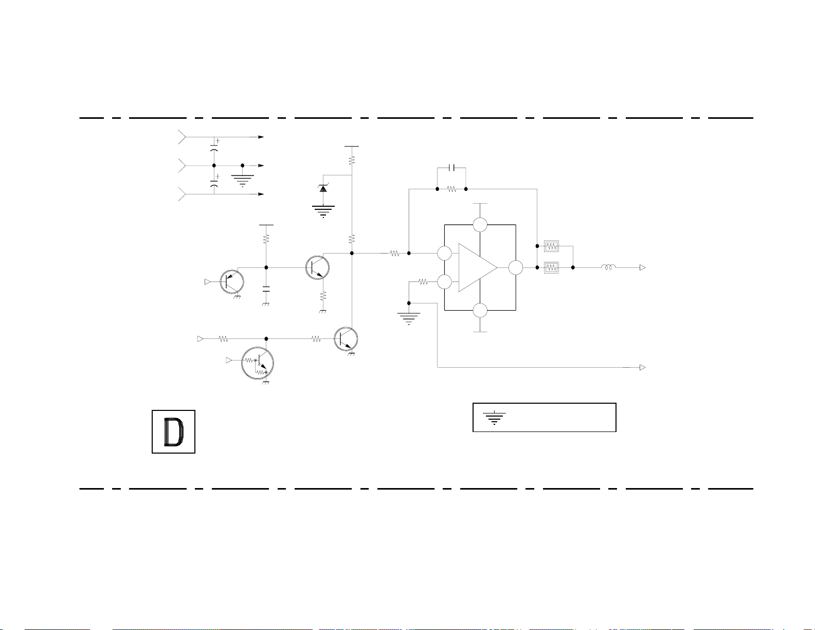
D BOARD POWER SUPPLY SECTION
Power Supply Electrical Circuit
The power supply is located on the D Board. It has three modes of operation that are controlled by a microprocessor. The
architecture is similar to discontinuous mode flyback converters and has photocoupler feedback for regulating the secondary
voltages. Circuit operation and troubleshooting are explained in the following sections:
Operation Modes Secondary Circuitry
AC Input Protection Circuits
Degauss Circuit Troubleshooting
Primary Circuitry
Operation Modes
The power supply has four modes of operation, ‘off’, ‘active off’, ‘suspend’ and ‘active on’. These modes are related to
power savings and are indicated by the front panel LED. Additional indications are failure diagnostics and aging mode.
The table below lists operation mode, condition and LED status.
Mode Syncs Condition LED
Of f NA AC Switch Off Of f
Active Off No H and V Low Power, Heater Off Amber
Suspend/ Standby No H or V Low Power, Heater On Amber 0.5s<- ->Green 0.5s
Active On H and V Present Phase Locked, Normal Operation Green
Failure 1NA HV or +B Failure Amber 0.5s<- -> Off 0.5s
Failure 2 NA H Stop, V Stop, Thermal Failure Amber 1.5s<- -> Off 0.5s
Failure 3 NA ABL Failure Amber 0.5s<- -> Off 1.5s
A
/Self Test No H and V Aging Raster or Test Pattern Green 0.5s<- -> Off 0.5s
Except for AC switch off, all modes of operation are controlled by the microprocessor located on the N Board. The failure
modes are detected by the microprocessor and the power supply is forced into active off mode. These functions are discussed later (Deflection).
With the AC cord attached to the monitor and connected to an AC source, the monitor will be off until the AC switch is
turned on. When the AC switch is turned on, the power supply starts and is in active off mode. The next step is active on
mode. The power saving modes are activated by the microprocessor based upon the presence of either H or V sync. If no
sync signals are present, the power supply is set to active off mode. If only horizontal sync is present the power supply
moves to suspend mode. If only vertical sync is present the power supply enters standby mode.
Power supply operation control signals are “Remote On/Off” and “Heater On/Off”. Remote On/Off is digital low for active
off and suspend modes. Heater On/Off is digital low for suspend mode. Suspend mode is similar to active off mode, but
with heater voltage on. To enter active on mode, the microprocessor must set remote on/off to digital high. Heater on/off is
also made digital high and the heater is turned on.
Output Off Active Off Suspend Standby Active On
B+ 0 120V 120V 180V
80V 0 55V 55V 78V
±
16.5V 0 8.7V 8.7V +16.5V
-16.5V 0 -12V -12V -16.5V
+12V 0 0 0 +12V
5V 0 +5V +5V +5V
Heater 0 0 3.2V 6.3V
±
H. Centering 0
5V
±
5V
±
8V
- 2 -
Page 3
AC input and Degauss
CN600
C605
C606
F601
250V
DGC1
VR601
RY601
4A
LF602
C601
R601
C602
C604
C603
R602
AC SWITCH
CN601
DGC2
THP602
TH600
R672
D601
12V
D670
R603
0.68
10W
Q670
R670
R671
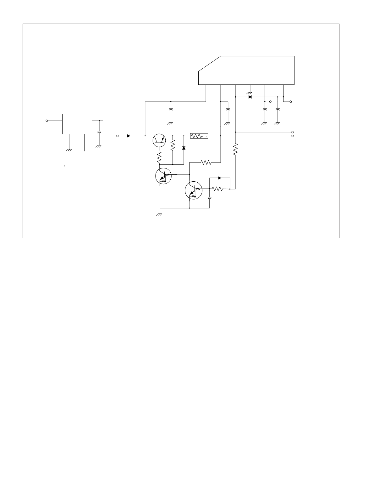
1. AC Input Section
The AC input section provides EMI filtering, input protection, surge limiting and CRT degauss operation. An AC switch is
also present for complete power off condition.
EMI Filter
The EMI filter comprises X-capacitors C601 and C602, Y-capacitors C603, C604, C605 and C606 and the line filter
transformer, LF602. Input protection is provided by F601 and surge current limiting by thermistor TH600 and resistors
R602 and R603. Degauss is explained in the next section.
The front panel AC switch is wired electrically between R602 and TH600 and when closed, completes the circuit. This
allows the bridge diode, D601, to full wave rectify the AC input voltage.
Degauss Circuit
The degauss circuit is used to demagnetize the CRT. After power on, the microprocessor located on the N Board sets the
degauss signal to digital high and through Q607 turns on relay RY601. This allows AC current into the degaussing coil
through posistor THP602. The current heats up the posistor and its affective resistance increases, this dampens the current
in the degauss coil to nearly zero. Duration time is approximately 5-6 seconds and the microprocessor then shuts off
RY601, which disconnects the degauss coil from the AC line. This operation should sufficiently demagnetize the CRT.
2. Primary Circuitry Section
IC601
The heart of the primary section is the AN8037 po wer supply controller, IC601. The following describes the functions of each
pin.
Pin 1 – TR - This is TR or transformer reset. Similar to a demagnetization function, this pin detects the falling edge of the
primary waveform during relaxation period. It allows the next conduction pulse only after reaching the bottom of the ringing
waveform. It contributes to the maximum on time setting.
- 3 -
Page 4

Pin 2 – OCP - Over current protection. Used to determine the overload level at which the timer latch is activated.
Pin 3 – CF – Oscillator. With a capacitor, determines the switching frequencies. (On/Off times.)
Pin 4 - CLM - Over current protection. If the voltage on this pin (primary current feedback) exceeds -0.18V, the power
supply will enter cycle-by-cycle current limit mode.
Pin 5 – GND- IC ground terminal.
Pin 6 – OUT- Output driver for switching transistor Q602.
Pin 7- VCC- IC supply voltage terminal. This voltage is nominally 17.5 volts during active on mode and 12 volts during
suspend or active off mode. The IC receives starting current via startup resistor (R613) until the auxiliary supply is availab le
from T601 VCC winding. If the voltage on this pin exceeds 19.4 volts (OVP), the power supply shuts off and can only be
restarted by disconnecting and reconnecting the A C line. Under v oltage lock out (ULV O) occurs when the voltage is less than
9.5 volts.
Pin 8 – SD- Used for OVP and timer latch functions. A capacitor determines the timing for OVP function.
Pin 9 - FB – Feedback terminal.
Operation
The power supply is a flyback type conv erter . It has both PWM and RCC characteristics. T he PWM controls the pulse width
of the gate drive. The RCC portion insures that the next conduction c ycle starts at zero v olts. Therefor e, the gate pulse wid th
varies and the switching frequency also varies. The on and off timing is determined by pins 3 and 1. Pin 1 detects the zero
voltage point or the valley on the relaxation ringing waveform.
When AC is applied to the power supply, start up current is supplied though R613 to pin 7 of IC601. Startup voltage is
approximately 15V. After start up, the voltage to pin 7 of IC601 is supplied through D605 connected to T601 pin 8. The f irst
mode of operation is active off mode and the VCC will be approximately 12 volts. The output drive pulse frequency will be
near 40kHz. or a type of frequency burst mode.
When the power supply enters active on mode, the switching frequency will vary between 65 and 120kHz., depending upon
input voltage and power lev el. The VCC le vel will be approximately 17.5 volts. O VP threshold is 19.4 v olts and UVLO is 9.5
volts. Therefore, if the VCC voltage is not correct, the power supply will not operate properly.
Feedback from the secondary side comes through IC603 and is connected to IC601 pin 9. (See diagram on page 5.)
3. Secondary Circuitry Section
The secondary section consists of the following circuits. Rectifier diodes and filters for all output voltages, horizontal
centering, +5/12 volt regulator, +5 volt back up circuit, heater voltage regulator, voltage feed back circuit, standby mode
feedback, B+ detection and protection circuits. This section will describe each circuit and its function.
Secondary Rectifiers
The secondary rectifiers supply the following voltages, 180V (B+) deflection and video, 80V video, ±16V deflection and
regulators and 8 volt heater regulator.
Horizontal Centering
This circuit supplies IC502, which is used to adjust horizontal raster position on the CRT. The horizontal centering circuit
consists of fusible resistors R621 and R622, diodes D648 and D649 and filter capacitors C656 and C657. In respect to the
secondary ground, the horizontal centering ground is floating and connected to –H DY line. The v oltages in reference to this
floating ground are ±8 volts. Care should be taken to not short the floating ground to the secondary ground.
+5/12 Volt Regulator
IC605 is the voltage regulator for +5 and +12 volt lines. The output voltages are supplied to the microprocessor, deflection
- 4 -
Page 5
From D601
R606 C615
From D601
D603
R608
R613
Q602
R609
FB
C619
VCC
OUT
IC601
D608
CLM
D605
D615
D633
R615
2
CCP
TR
18
17
16
15
14
13
12
11
10
IC606
D656
D653
D654
D655
D652
-16V
-16V
PROTECTOR To IC604
16V
16V
D651
D650
D649
To HDY-
D648
To
IC501
Pin5
Q658
5V
Q605
80V
180V
To IC502 Pin 3
D631
16V
IC603
D632
Q656
IC652
REMOTE ON/
3
OFF
Q657
PWR
SHUTDOWN
R660
1
R663
2
R659
R668
C613
180V
T601
SRT
2
5
7
8
9
C614
14679
and video circuits. The +16.5 volt and the 8-volt lines supply the input v oltages for +12V and +5V re gulator sections, respectfully. During active off or suspend mode a standby back up circuit supplies the 16.5-volt line to the +5 volt section.
+5V Standby Circuit
Normally , the +8V line supplies the +5V regulator. During activ e off or suspend modes, the voltage supplying the +5 re gulator ,
IC605, will become very low . In order to pre v ent loss of the +5V, it is necessary to supply a back up v oltage. Supplying +16. 5V
line to the regulator through Q601 does this. Note: at this time the +16.5V has been reduced to 8.7 volts.
In Acti ve of f mode, Q607 is off, Q606 is on and Q601 is on. Through Q601, IC605 receiv es its input voltage for +5V. In Acti ve
On mode, Q607 is on, Q606 is off and Q601 is off. Since Q601 is off, IC605 must receive the +8 volt line through D610.
There is a time delay in this circuit, which is used to insure that during any transitions, the +5V line does not drop out. These
components are C636, R638 and D619.
Heater Voltage Regulator
Heater filament voltage is supplied by the 8-volt line and is re gulated by IC604. Heater on/off is used to turn the output on or off.
This is found at pin 4, VC. The output is off during active off and suspend modes.
Feedback Circuit
The feed back circuit is divided into two sections. One is for active off and suspend modes, the other for active on mode.
The following two sections explains the theory and operation.
Active Off and Suspend Mode Feedback
Feedback is provided by circuit elements IC603, D632, Q658 and Q656. The 16.5V line is regulated and the actual voltage
is 8.7. Due to this condition, B+ is no longer regulated and is reduced approximately 67%.
During active off and suspend modes, remote on/off is low and Q656 is off. Current flows through D632 when the 16.5 V
line is greater than 8.2 volts. This current biases Q658 and current from IC603 is allowed to sink to ground. The 16.5-volt
line supplies this current to IC603. The current through IC603 biases its transistor and sinks current from IC601 pin 9. IC601
then responds accordingly and adjusts its duty cycle in order to make the output voltage reach 8.7 volts. This completes the
feedback loop.
- 5 -
Page 6
+8V
IC604
PQ6RD83B
Heater
Regulator
1
I
G
34
VC
Heater
ON/OFF
Feedback Circuits
IC605
TDA8138A
2
1
T
T
U
U
P
P
N
I
IN
12
C623
Heater
2
O
out
D610
+8V
Q601
+5V BACK UP
R636
Q606
R635
R617
D618
R637
D619
C662
DISABLE
GND
4
3
R666
6
D607
C634 C635
OUTPUT 1
OUTPUT 2
7
+5V
REMOTE ON/OFF
+16V
Q607
R638
C636
When remote on/off is set high, Q656 is turned on and Q658 is turned off; this disables active off and suspend modes
regulation loop.
Active On Mode Feedback
As stated earlier, when Q656 is on, the acti ve of f and suspend mode re gulation is disabled. At this time, IC652 takes o ver and
the B+ line is regulated. IC652 is a shunt regulator and regulates the B+ voltage by sinking current from IC603 to ground.
The reference voltage at pin 2 determines the sink current into pin 3. The reference voltage is set to 2.495 volts by resistor
divider R659 and R660. Since the B+ is connected to the resistor divider, any changes in voltage is detected at the reference
terminal; the shunt regulator then tries to force the reference voltage to 2.495 volts by sinking more or less current into pin 3.
As mentioned before, IC603 biases its transistor accordingly and IC601 responds by changing the switching duty cycle in
order to keep the output voltage at 183 volts. The other components connected to pins 2 and 3 are for compensating frequenc y
response. This completes the feed back loop for active on mode.
4. Protection Circuits
There three protection circuits: OCP, O VP and secondary short circuits. OCP is pulse by pulse and is performed on the primary
side. OVP detects e xcessive output voltages. To detect secondary side short circuits, there is a circuit called B+ detect and it is
monitored by the microprocessor. The following will explain the operation of these functions.
OCP
OCP is activated if there is too much current passing through the power MOSFET, Q602. This condition will occur if either
the B+ line or 80 volt line is shorted.
R609 is the current sense resistor. Current through this resistor will cause a negative voltage drop in reference to ground.
R608, R606 and C615 couples this voltage drop to IC601 pin 4. If the voltage level exceeds –0.18 volts, the IC sets pulse by
pulse current limit and the output voltages are in affect very low. This condition is often audible and characterized by a
‘chirping’ sound.
OVP
The function of OVP is related to IC601 and the threshold is approximately 19.4 volts. This is sensed at pin 7 of IC601. Under
- 6 -
Page 7
normal operation, the VCC voltage is 17.5 v olts. In the e vent the re gulation loop was open or the control loop fails, the outp ut
voltages would rise rapidly. Likewise VCC will rise and when the threshold voltage is reached, IC601 would latch up. This
condition disables the output circuit at pin 6 and the power supply will not operate. Since the IC is now latched, only turning
the AC switch off and then on again can restart the power supply.
5. Secondary Short Circuit
B+ detect purpose is for determining secondary side short circuits. Sensing the node voltage of resistor divider R611 and
R612 does this. R611 is connected to +5V and –16.5 is connected to R612. If the node voltage exceeds 2.0 volts, the
microprocessor sets PWR Shut Down to digital high. In this event, Q657 is turned on and feedback current is bypassed to
ground from IC603. This causes unregulation and the output voltages become high. The VCC winding on the primary side
reflects this condition and exceeds 19.4 volts, which will cause IC601 to latch and disable the power supply. Turning the AC
switch off and then on again can only restart the power supply.
An additional short circuit protect is provided if the +12V, +5 or 3.3V lines are shorted. This is through circuit elements
D641, Q640 and Q657. During normal operation, through D641, the +5 volt line biases Q640 on. The 80 volt line is
connected to the collector of this transistor through R641. When the transistor is on, the collector voltage is nearly zero. This
point is connected to Q657 through R642 and Q657 is still off. If there is a short on any of the lower voltage lines, the +5
volt line will become lower than 3 volts and Q640 will turn off. In this case the collector voltage rises and Q657 will turn on.
Then through Q657 the feedback loop current is shorted to ground and causes OVP, which is sensed by IC601.
TO IC601
Pin 2
Q658
2SC3311A
ISS119
IC606
PC123FY2
TO IC601
Pin 9
D631
IC603
PC123FY2
FEED BACK
Q658
2SC311A
ACTIVE OFF
REGULATOR
Protection Circuits
3
2
5V
Q605
DTC124ESA
IC652
TL431BCLPRA
Remote ON/OFF
16V
1
Remote ON/OFF
180V
Power shut down
Q657
DTC124ESA
OVP
D640
1SS119
C640
2200p
R642
10K
80V
Short circuit
Protection
Q640
DTC124ES
5V
- 7 -
Page 8

6. Troubleshooting
Warning
Before attempting to fix the power supply, safety should be consider first. Never connect test probes to the primary side
circuits, unless proper isolation has been installed. If isolation for the AC mains is not present, serious harm can occur .
Never assume you are safe.
No Power
In the event that the monitor does not turn on, first check F601 and R615. If these parts are blown, the primary side circuitry
should be checked. If the fuses are not blown, then check the secondary side circuitry, especially the protection circuits. If
these circuits are causing a no power symptom, the problem can be more readily found.
AC Input and Degauss Circuit Trouble Shooting
For no power or nonoperating power supply, the AC input circuitry should be checked. Open or short circuit elements will
cause non-operation. F601, CN600, CN603 and CN2003 On the H Board should be checked first. The wiring between the
AC switch on the H Board and D Board should be checked. Check the front panel AC switch for continuity.
If all elements are correct, check whether F601 breaks when power is applied and the AC switch is closed. If the fuse does
blow, there may be problems with the primary circuitry or a component short.
The degauss will malfunction if CN601 is not connected. One problem could be loss of degauss signal from N Board. This
can be verified by using the manual degauss command found in the OSD menu. If the signal does not appear at R670, then
check the signal on the N Board and all connections. It is possible that the microprocessor does not function correctly .
The second step is to place a short across the AC terminals of RY601 for less than two seconds. If degauss operates then
check Q670 and RY601. If degauss does not work, check THP602 for an open condition and VA601 for a short condition.
Primary Section
Three main areas can diagnose primary circuit failures. These are IC601, Q602 and Feedback system.
Visible checks of these areas will aid in finding problems. The following will discuss each section.
IC601
First apply AC to the monitor and check IC601 pin 6 output. If the output on pin 6 is not present or briefly appears, there
could be problems with Q602 and related parts. Further, check VCC level at pin 7. If it less than 9 volts, the IC could be
in latch mode. If the voltage is very low, there could be a short on any of the IC pins. In reference to ground check the
impedance of pin 1, 6, 7 and 9. If any of these pins are shorted, replace the IC and check components connected to the
related pins. Pin 1 is especially vulnerable to damage. Take care that C619 and C616 are fully discharged before replacing
the IC.
Q602
The switching transistor can be damaged in various ways. These are related to voltage, current and temperature.
Check whether the transistor is shorted across drain and source terminals. If there is a short, R609, R615 and FS601 should
be checked. R609 is usually broken when Q602 fails. Additional components to check are D603, D604 and IC601. If
Q602 is shorted, all these parts should be replaced.
Failure of a secondary rectifier diode can also cause Q602 to fail. Check B+ and 80V diodes for open or short conditions.
There is also a clamp circuit, which is used to clip the turn off spike found on Q602 drain. If the clamp circuit is broken, it
can cause Q602 failures. Check D615, C622 and R619.
Secondary Circuit
Failure in the secondary circuits can be categorized by rectifier diodes, fusible resistors, regulators, +5 volt back up circuit,
feedback loops and protection circuits. These sections are interrelated and failure in one can af fect another. Consequently,
some failures will also affect the primary circuitry.
Rectifier Section
Rectifier diode failures are not common, but do occur. Deflection, video and N Board failures contribute to diode damage.
In the event a voltage is not present, check for shorts to ground, open or short diodes. Also check fusible resistors or any
zener diodes found on the voltage lines.
- 8 -
Page 9

Horizontal Centering
Loss of horizontal center adjustment can be affected by the rectifier diodes, fusible resistors, IC502 and related circuitry.
Measure the voltages in reference to the horizontal centering ground. Typically, the voltages are ±8 volts. However, the
adjustment setting can reduce the voltages by 1 volt. If there are no problems found with the diodes or fusible resistors, the
next step is to check the adjustment signal at Q517. If the adjustment signal is not present check the N Board and connections. Otherwise, check IC502 and related components.
+5/12 Volt Regulator
Loss of voltage due to shorts or device failures on either +5 or +12 volt output lines can occur. Consequently, IC605 can
be damaged and need replacing. Before replacing IC605 check for shorts or damaged parts along the output lines. If +12
volt does not appear, check the remote on/off signal. The N Board supplies this signal and it may be necessary to check it
and all connections.
+5 Volt Standby Circuit
Failure of this circuit can be affected by IC605. The remote on/off signal controls circuit operation and it may need
checking. In case the circuit does not work properly, check D619, R617 and Q601. If these components are good, check
the remaining circuit parts.
Heater Voltage Regulator
This circuit may be affected directly by fusible resistor R654 or D654. If these parts are good, check the regulator output
for a short to ground. Shorts can occur on the video board. In the case of an output short, IC604 may have been damaged.
If the IC appears to have no damage, check the connections and N Board for any problems with the heater on/off signal.
Feedback Circuit
Problems with feed back can cause power supply shut down or low voltages. First determine whether the power supply is
operating in active off, active on modes or not at all.
The power supply can be stuck in active off mode. The remote on/off signal, Q656 and IC603 can affect this condition.
Likewise, if the power supply is always in active on mode, the same items should be checked.
Checking for voltages at IC603 pins 1 and 2, IC652 pins 2 and 3 can solve more difficult problems. Additionally, IC603 pin
4 and IC601 pin 9 should be checked. If there are problems with these devices, B+ or 16.5 volt line, the feedback systems
will not work correctly. Also check the protection circuits.
Protection Circuits
OCP occurs when there is excessive current through Q602. Failures with Q504, Q505 or the video section commonly
cause this condition. These areas should be checked. OCP condition can also occur if R609 is open or if there are problems with IC606 or Q605.
OVP usually occurs when the feedback loop is open, secondary voltage shorts or loss of +5 volts. Isolate the OVP trigger
condition, by first checking the operation of the feedback loop and Q657. Either PWR shutdown or Q640 can turn on
Q657. The feedback loop can be verified by removing Q657 and measuring the B+ voltage level.
- 9 -
Page 10

D BOARD DEFLECTION SECTION
1. Horizontal Deflection Circuit
Overview
These circuit drive the DY(Deflection Yoke) for Horizontal Deflection. The H size and H shape control (IC805 and around) is
included in this page as well.
H Drive, H Out, Feedback
HD pulse supplied from N board is inverted by Q501 and switch Q504 through Q502,503. The drive current which
introduced in HDT by this switching will drive Q505(H OUT) and 1000v pulse appears on collector. D504 is the “Damper
Diode” which avoid the negative pulse and discharge the energy for next Horizontal Drive. Q514 is the buffer for the “H
FBP” feed back to N board and it will be the reference of phase/jitter control of DSP. T504( HST) is to sense the deflection
current going to DY. The voltage appeared on secondary side will be the feed back for H Size/Shape control.
H Size/Shape control
HD pulse also triggering the H Size/Shape control IC805 (pin#8). IC805 is “PWM IC” and it controls H and HV B+
chopper duty. H Shape coming from N board is already including the Size Information(DC Level). It will be supplied to
IC805 (pin#2) after pulled up to 12V through R813. H Reg Output(pin#20) is switching pulse of Q506(B+ chopper). The
energy supplement from 180v to H Def circuit (through T502) is controlled by the duty of this pulse. The H Shape input
and feedback voltage(pin#20) from T504 are compared by error amp (in IC805) and H Reg out pulse duty is controlled to
keep the level of these two the same.
T roubleshooting
See attached “FLOW CHART” and confirm if it’s really H Deflection issue.
No H Deflection / No Power
Check Q505, Q506 and D504 first. In case any of these shorted, check T501, Q504, R507 and D502.
Those parts might have been damaged.
If both of Q505, 506 were not broken, check the HD pulse at the gate of Q504.
If no pulse, check Q502, Q503, Q504.
Otherwise, check R512, D503 or try changing IC801.
Bad Distortion
Check pin#2 of IC805 and confirm that proper DC level and AC waveform.
If the distortion is on only right side, check all above (“No H Deflection”).
Otherwise, refer to the Troubleshooting of next section (“H Lin and Ringing Correction”).
- 10 -
Page 11
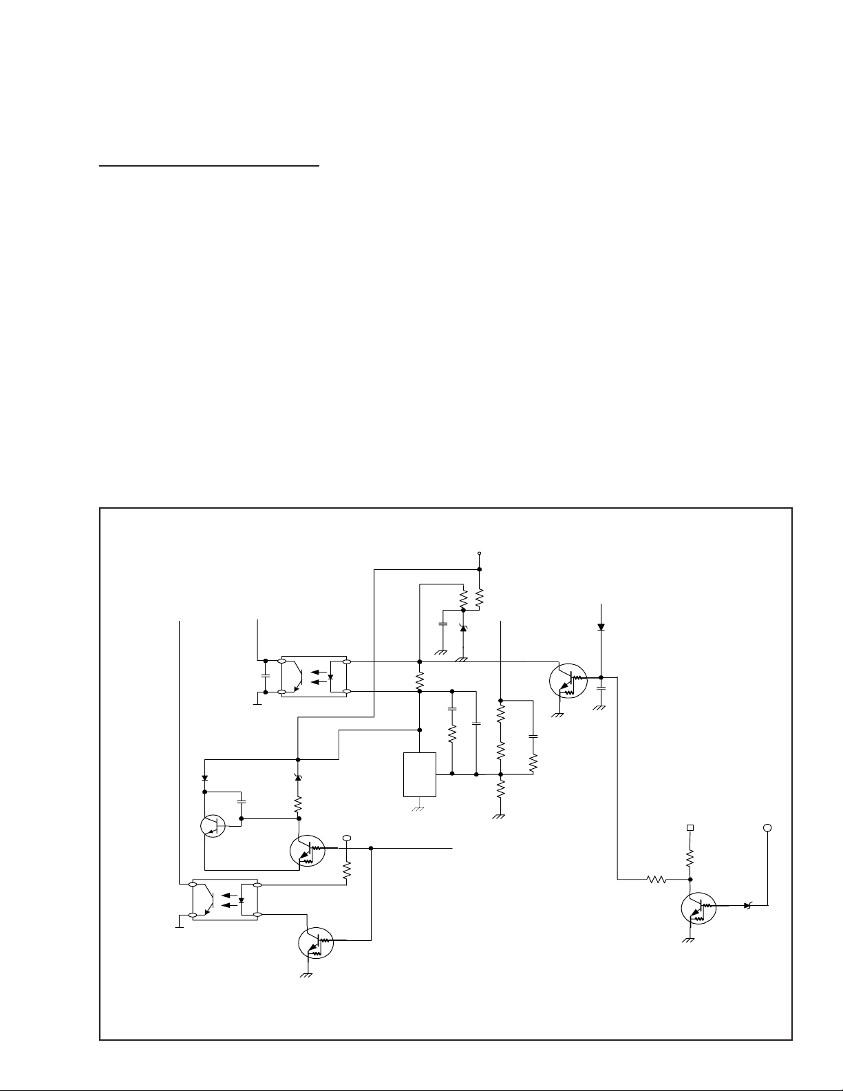
H Deflection Circuit
R517
R518
320
H DefINH Reg
Out
PWM IC805
H SHAPE
12V
2
7
H SHAPEINHD
IN
28
R512
- 11 -
R813
D503
D505
180V
L501
Q506
B+CHOP
5
2
Q518
12V
TO:
H Lin and
Ringing Circui t
4
HDYHDY-
3
CN801
HD out
T501 HDT
12V
1
12V
6
4
Q502
2
Q501
6
Q504
D502
T502
HOC
D504
C507
3
T504
2
HST
5
1
Q514
H DY+
2
H DY+
1
H FBP
TO CN801
#32
Q505
Q503
H-OUT
R507
-16V
Page 12

2. H Linearity and Raster/Distortion Ringing Correction Circuit
This section includes HLC Control circuit which is new in D98, S cap switching and HLC/S-Cap Damping circuits. These
circuits are placed directly on the “cool side” of DY which is in series with deflection current line.
H Centering circuit will be explained in next section.
HLC Balance Control and HLC damping
There is no HLC switch for this chassis. Instead of that, HLC(L502) effectiveness is changed by LCT(503) for each Fh
since T503 and L502 is in parallel. LCT is Cross Transformer which can change its inductance accordingly to the DC
current of secondly side. The current of secondly side controlled by DAC output of MICRO through Q507. *It can be
changed by register “HLC BAL”. R520 and C528 is damping circuit to avoid the Raster Ringing (mainly on left side of
picture) caused by HLC, DY and S-caps.
S-Cap switching and S-cap Damping
H Def current is distorted by resonance between S-Cap and DY to correct the linearity. Since the resonance frequency has
to be changed for each fH, S-Cap switching is controlled by MICRO
Switches are "On" when its gate is Hi(5V) and that moment, drain voltage should be grounded (0V).
L505, R522 and C513 is damping circuit to avoid Distortion Ringing (mainly on top of the picture) caused by S-caps and H
Control loop gain. L504, R523 and C527 is also the same purpose as above but only works when Q508 (Switch for the
Biggest S-Cap) is “On”.
Troubleshooting
See attached “FLOW CHART” and confirm if it’s really H lin issue.
Bad Linearity
Confirm that Raster is approximately in the center of the Bezel. If not, refer to next section (Raster Centering Circuit).
Check S-cap switches (Q508, 509, 510, 511, 512, 513) and confirm that H Linearity changes proportional to the value of
“S-Cap Direct”. Confirm that H LIN BAL changes by the register value of ”HLC Balance(Max/Min)”.
If it’s not working, check Q507 and the connection between N bd and D bd or, Check L502, T503.
Bad Top Distortion/ Left side Raster Ringing
Check damping circuits explained above or check the connection between N & D(HLC control line).
3. H. Raster Centering Circuit
Overview
H Centering is changed by supplying DC current to DY. D98 is taking the common level on DY cool(-) side and +/- 8V from
power supply transformer(T601 PIN#10, 11, 12. #11 is the common).
H Center Circuit
The DC current is outputted by powered OP-amp(IC502). This circuit is making “invert amp” with the gain of R549/R548
and input 1S Q515 collector. The level is controlled by MICRO”H CENT’ through Q517(buffer). Q516 is Stand by-MUTE
switch which activates when “Remote On/Off’ is Off(Lo).
Trouble Shooting
See attached “FLOW CHART” and confirm if it’s really H Center Circuit issue.
No Raster Centering Control
Check R621, 622(Right next the SRT) first. If it’s open, change IC502.
Confirm that voltage of Q5 l 5 base is changing accordingly to “H CENT MAX or MIN” register.
If not, change Q517 or check the connection between N and D.
Confirm that Q516 is Off. This circuit should not work when the Monitor is in Main mode.
Check IC502.
CAUTION!!
The heatsink of IC502 is connected to the H center(-) level, not GND! It could have up to 150V and should not be
touched to any other metals.
- 12 -
Page 13
H. DEFLECTION
CIRCUIT
H DY+
H DY+
H DY-
R520
C528
100
330p
2W
2kV
:RS
B
TO H. CENTERING CIRCUIT
2SK2098
R527
47k
4
S
Q509
C517
0.01
C518
0.68
250V
:PP
:PT
C521C522
R530
0.068
250V
:PP
Q512Q513
47k
IRLI530GIRLI530G
0.01
:PT
1
S
- 13 -
0.033
400V
:PP
C526
0.01
:PT
0
S
R529
2
S
0.15
250V
:PP
47k
C524C525
0.01
:PT
C519C520
0.33
250V
:PP
Q510Q511
IRLI530GIRLI530G
R528
47k
C523
0.01
:PT
3
S
R525
C515
L504
1.5
10mH
250V
:PP
47k
R543
47k
R536
SSSSSS
1M
C516
Q508
47
2SK2098
:PT
5
S
R523
1/2W
:FPRD
C527
4.7
250V
47
C514
0.17
400V
:FPRD
C513
2.2
250V
T503
:LCT
Q507
2SC2785-HFE
HLC CTRL
L505
2.2mH
R522
47
1/2W
6
2
1
R526
39
:RN
L502
:HLC
5
C537
0.22 :MPS
C511
0.22
:MPS
1
2
9
R519
2.2k
R747
7
L
A
B
N
I
L
.
H
C512
10
:FPRD
10
16V
H DY-
BOARD
H. LINEARITY AND RASTER/DISTORTION RINGING CORRECTION CIRCUIT
Page 14
FROM D648 IN P.S.
C656
HC+
HC+
R547
C538R545
R549
2
1
HC+
5
IC502
-
R546
TO H. DY(+) VIA T50
4
L503
(DRAIN OF Q506)
+
R541
3
HC-
!!!
IMPORTANT !!!
TO H. DY(-) VIA L50
R551
HC N
HC-
C545
Q515
D511
R550
R548
R542
Q516
STBY SW
R552
FROM PIN# 11 T601
FROM D649 IN A.S.
C657
Q517
- 14 -
H. CENT
R815
16V
REMOTE ON/OFF
Q802
CENTER VOLTAGE
=
COMMON
(ISOLATED)
(BOARD)
(19D98 H. CENTERING CIRCUIT)
Page 15
Rotation/Vertical Key Circuit
+5V
R735
Rotation Coil(CN702)
R775
R708
0
R709
C701
R707
C702
IC702
+16V
4
-16V
5
1
V+
+
V-
-
2
3
0
0
R736
R737
R729
C705
42
0
40
N-BOARD
D.TILT
59
IC1002(DSP)
ROTATION
3
IC1001
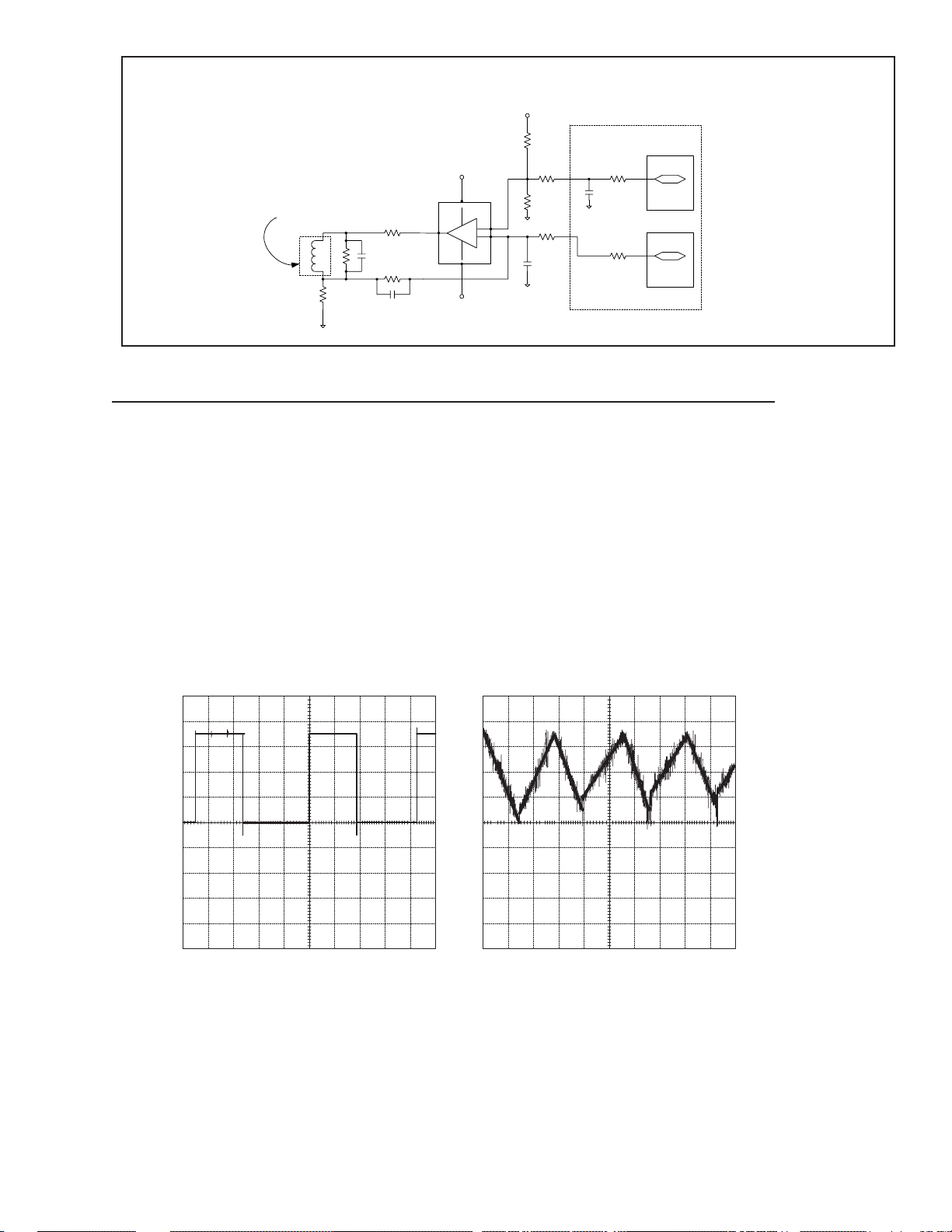
4. Rotation/Vertical Key Circuitry Mounted on the D/N Boards) Circuit
Theory of Operation
The Rotation/Vertical Key circuitry takes its input from the N-board via pins 40 (Rotation) and 42 (D.Tilt). D. (Dynamic)
TILT is generated by the DSP (IC1002) while Rotation is generated by the microprocessor (IC1001). Rotation is a PWM
waveform at approximately 40kHZ measuring 5V pk-pk at pin #3 of the microprocessor. While D.TILT is a triangular
waveform at the vertical scan rate, 1.0Vpk-pk in amplitude centered at 1.5V. Typical waveform patterns are provided as
figures #1 and #2 below. Rotation is filtered by the R729 and C705 combination and a DC offset is added to D.TILT from the
+5V line via R735. These two waveforms are added together and amplified by IC702. This amplifier is a transconductance
amplifier (it amplifies a low-level voltage into a high level current). The output current from pin 4 of IC702 flows through
R709 and the rotation coil and returns to ground through R708. The feedback is sensed at R708 and sent back to the amplifier
through R707. The DC level of the current through R708 is controlled by the Rotation signal while the triangular currant
amplitude is controlled by the D.TILT waveform.
FIGURE 1 FIGURE 2
T1 21.60us
T2 150ns
DT 21.75us
T1 1.10ms
T2 2.60ms
DT 13.70ms
Vertical Key Circuit Troubleshooting Hints
It is possible to have a malfunction of only the Vertical Key portion of the circuit. This can occur by a loss of signal from
D.TILT. First check if the Rotation function is working properly. There should be no more them a +/-15 degree picture
rotation by operating the rotation function through min-max extremes. When the Rotation function is at its full position (SV
at R729) the voltage at R708 should be a positive 2.25 vdc, approximately. And at its full negative position this voltage
should be a negative (-) 2.5 vdc approximately (NOTE: if D.TILT is open or shorted to ground these voltages will not be well
centered around 0V).
- 15 -
Page 16
Signal tracing should begin at pin 59 of IC1002 on the N board. The triangular output waveform at this point should change
+/-1 vdc by operating V.TrapSawBtm and V.TrapSawTop registers through function through min-max extremes. This same
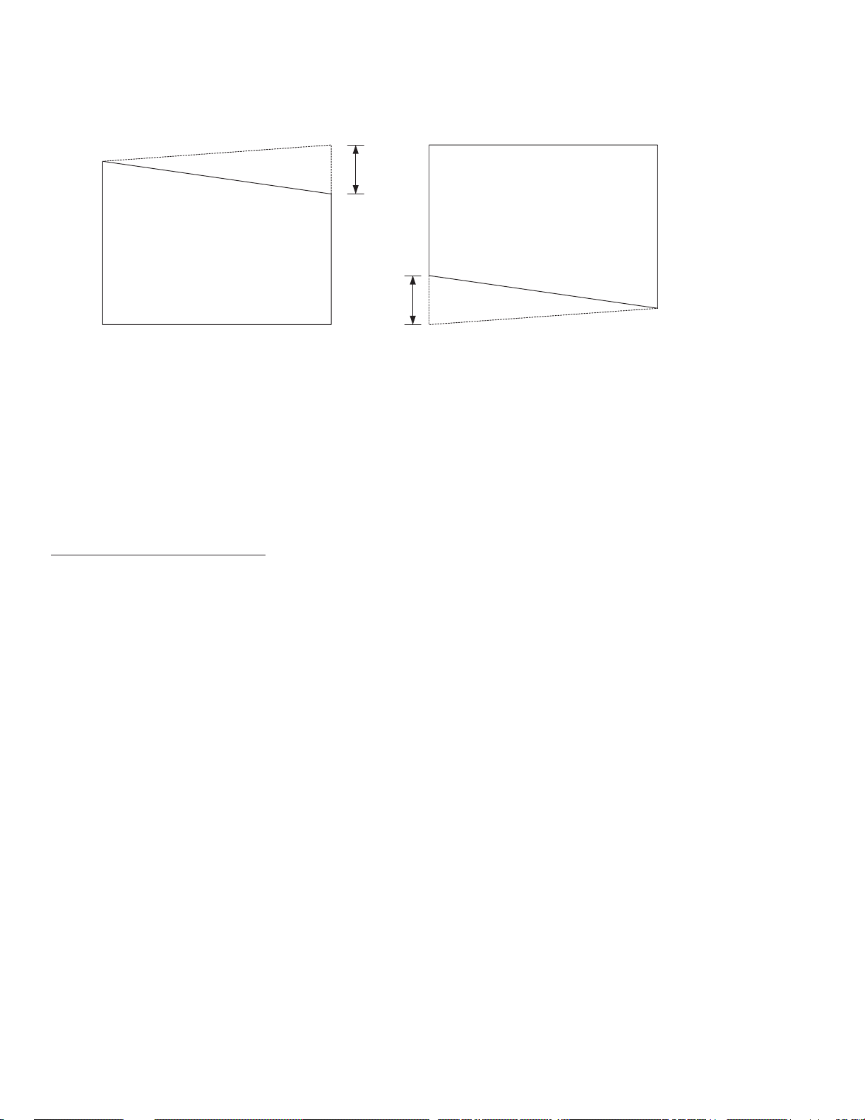
signal should appear at pin 42 of CN801 and at the input side of R736. Screen movement for this function is as shown below:
1.5mm
1.5mm
V.TRAPTOP
(Dashed lines Indicate
Negative movement)
Movement
V.TRAPBTM
(Dashed lines Indicate
Negative movement)
Movement
Rotation Circuit Troubleshooting Hints
If Rotation does not work Vertical Key will not work. Signal tracing for a rotation problem can start at pin 3 of IC1001. The
Rotation signal will be a square waveform at 40kHz. This signal is filtered at the R729, C705 combination. If this waveform
is reaching R705 the problem is in the IC702 area.
5. Dynamic Focus Circuit
Overview
Both H and V Dynamic Focus Waveform originally formed by DSP.
H DF is amplified by Hi-speed OP Amp and also Transformer.
V DF is amplified by Transistor inverter.
H DF
IC703 is amplifying the H DF waveform formed by DSP. The voltage is re-amplified by T701 to about 600Vp-p and supplied
to FBT.
V DF
V DF waveform is buffered by Q707 and amplified by Q706 to about 200vp-p.
300v Vcc is made by FBT through D906. This voltage is also used for HV Protector.
Troubleshooting
See attached “FLOW CHART” and confirm if it is really a DF issue.
Bad H DF
Confirm that waveform from N board is correctly there(1Vp-p).
Check the voltage of pin#6 of IC703. If no output, change IC703. If there is wave form, change T701.
Bad V DF
Confirm that waveform from N board is around 3Vp-p. If it’s more than 3.3Vp-p, change the N board.
Check 300v from FBT.
- 16 -
Page 17
Dynamic Focus Circuit
+16V
H. DF FROM N BOARD
C707
V. DF FROM N BOARD
R723
Q706
R724
R734
H. DF TO FBT
PIN# 14 VIA R9
T701
:DFT
12
11
10
9
7
6
R742
V. DF TO FBT
PIN# 15 VIA R909
C711
2
3
4
5
C714
R733
R738
C728
R754
D905
R917
8
6
+16V
9
5
-
IC703
4
+
7
-16V
300V
C931
R727
Q707
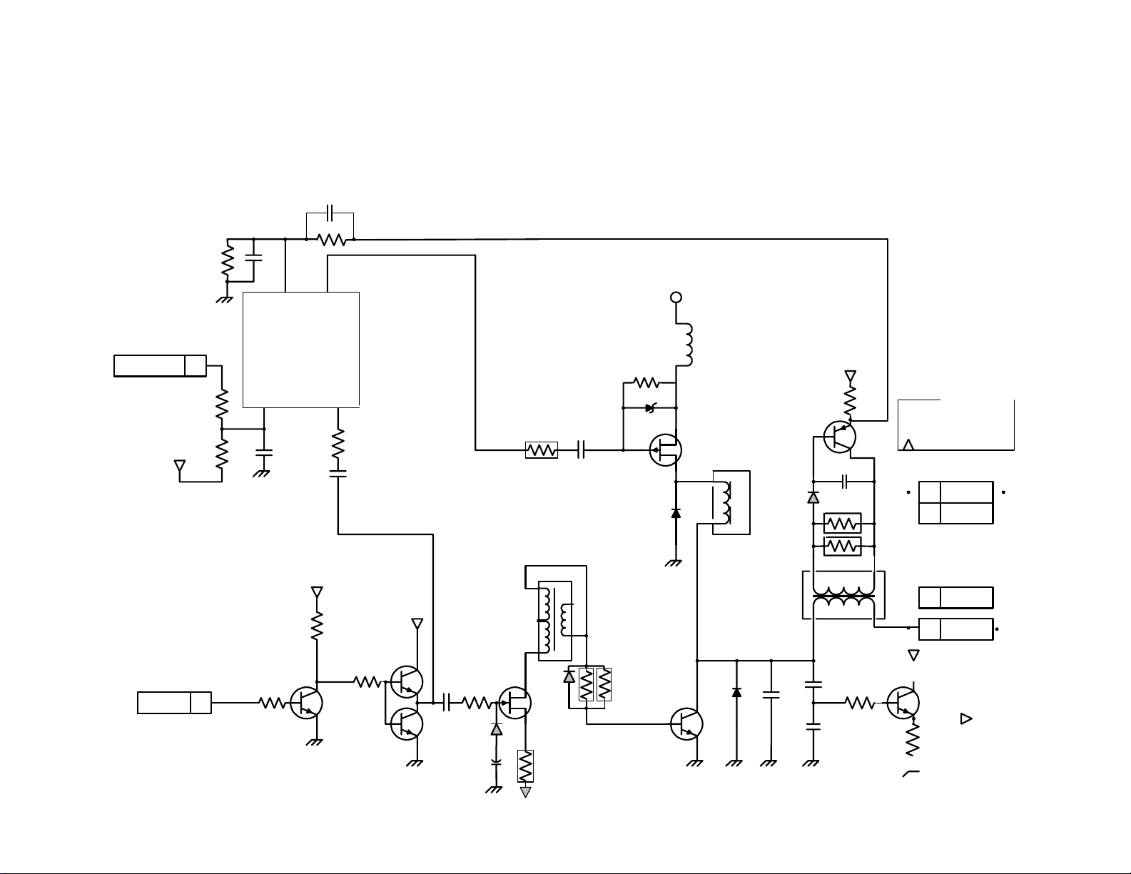
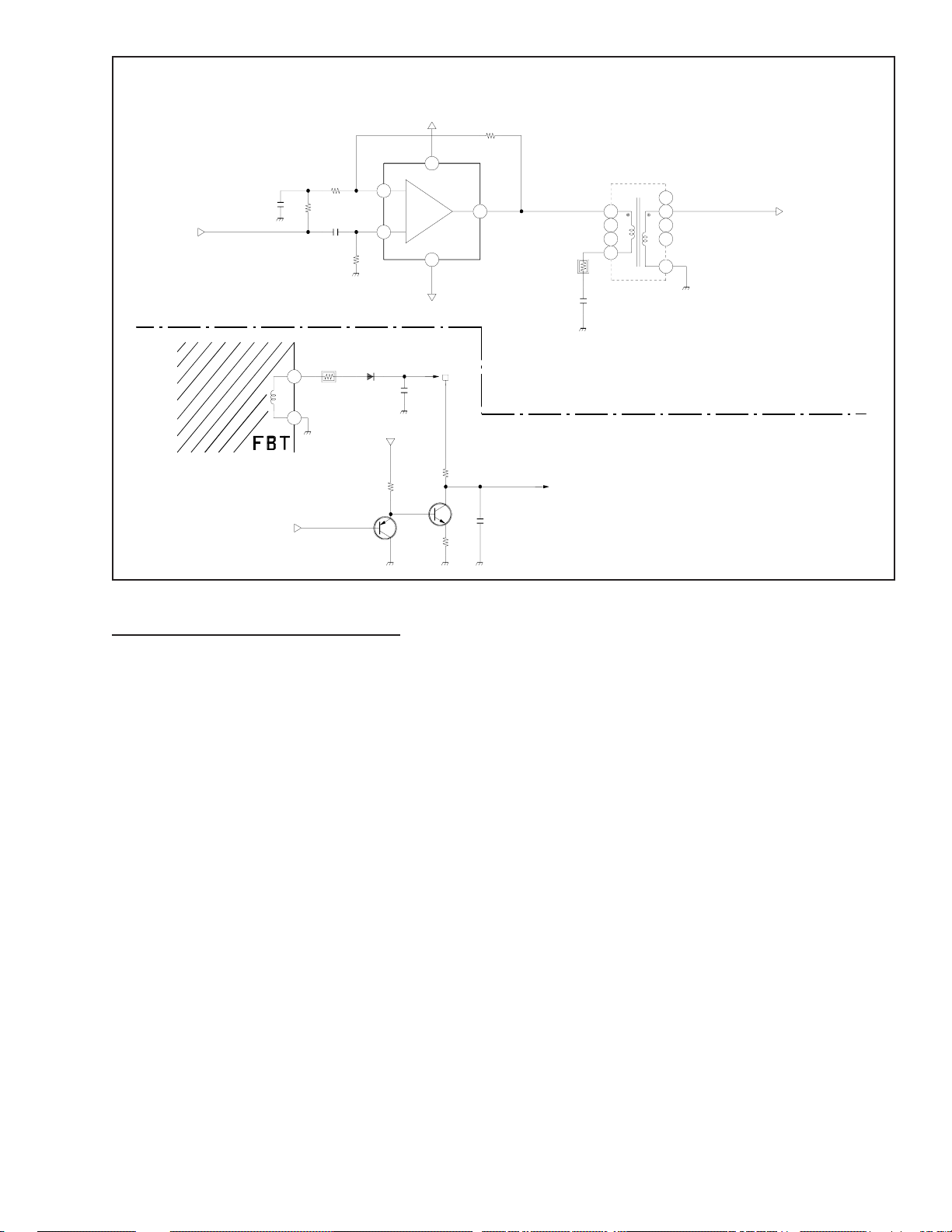
6. High Voltage Protect Circuit
This circuit generates the High Voltage supply for the anode and G2 (1000V) of the CRT. It consists of a high voltage driver
and regulator similar to a switching power supply function. In addition, there are High Voltage and Beam Current protection
circuits. All those circuits are similar to N3 or D1 chassis circuits.
High Voltage Regulation and Output Circuit
The HV Drive pulse is generated by IC805 and synchronized with Horizontal drive pulse. It is supplied to the Gate of Q902
the HV Out FET .
The HV Out Pulse approximately 700V, is generated by Q902 switching with the peak voltage being controlled by the
switching duty of Q901 (B+ chopper). Internal resistors and R903 and RV904 divide HV generated in the FBT. Since this
voltage is the feedback for HV Regulation control. Adjusting RV904 will result in changing the HV Regulation level(= HV
level). HV Feedback voltage is returned to IC805 at pin#12 to be compared with an internal reference voltage of IC805 at
pin#13. According to this feedback level, IC805 changes the pulse duty cycle. This pulse is felt at pin #18 of IC805 thereby
controlling the output of B+ chopper drive Q901.
G2 Voltage
G2 voltage at approximately 1000vdc is produced by the FBT rectifying the output voltage of T901 pin#2 through D906 and
C933. This voltage will be supplied to A board via CN 510, which contains the G2 control circuit.
HV Protect Circuit
HV Protect circuit will be activated by the Microprocessor when the signal at HV DET, CN801 pins#24 reaches a +5vdc
level. HV DET indicates the level of the primary current developed by the 300V winding of the FBT through R921, D908.
Beam Current Protect
Beam Current Protect will be activated when ABL DET at CN801 pin#1 reaches a level of 0V when operating in main mode.
ABL DET level is corresponding to the Beam Current which is supplied to FBT through R914 and D909. The voltage current
relationship is inversely proportional Volta ge (down) Current (up).
- 17 -
Page 18

Troubleshooting Hints
See attached FLOW CHART to confirm if is really an HV/Protect Circuit issue.
No HV / No Power
Perform basic checks of Q901 and Q902 first. If both Q901 and Q902 were not broken, check the HV Drive pulse at the gate
of Q901. If no pulse, check R911 and D903. Otherwise, check R910, D901 or try changing IC805.
No G2 Voltage
Check R918 and D906.
Protect Malfunction
To see if HV Prot or ABL Prot are suspect check the Shutdown Log data at the Shutdown Log register. Refer to Shutdown
Log Table below.
When an HV Shutdown is indicated, check all N board connections, R917, R921 and D905 or, replace T901 (FBT).
Where ABL Shutdown is indicated, check the voltage T901 pin#11.
If it is higher than 0.5v immediately prior to shutdown, check connections all the way to N board. Should the voltage reach
and remain at the 0 volt level, even after the first 2.0 seconds of Power On, check D909 and 904 or check White Balance.
SHUTDOWN LOG TABLE
Bit Register value Shutdown Mode Comment
bit7 128 N/A N/A
bit6 64 B+ Shutdown Explained later
bit5 32 S cap Shutdown Explained later
bit4 16 ABL Shutdown Hardware Controlled
bit3 8 HV Shutdown Hardware Controlled
bit2 4 HV U Shutdown Not Used
bit1 2 No Vertical Explained later
bit0 1 No H Pulse Explained later
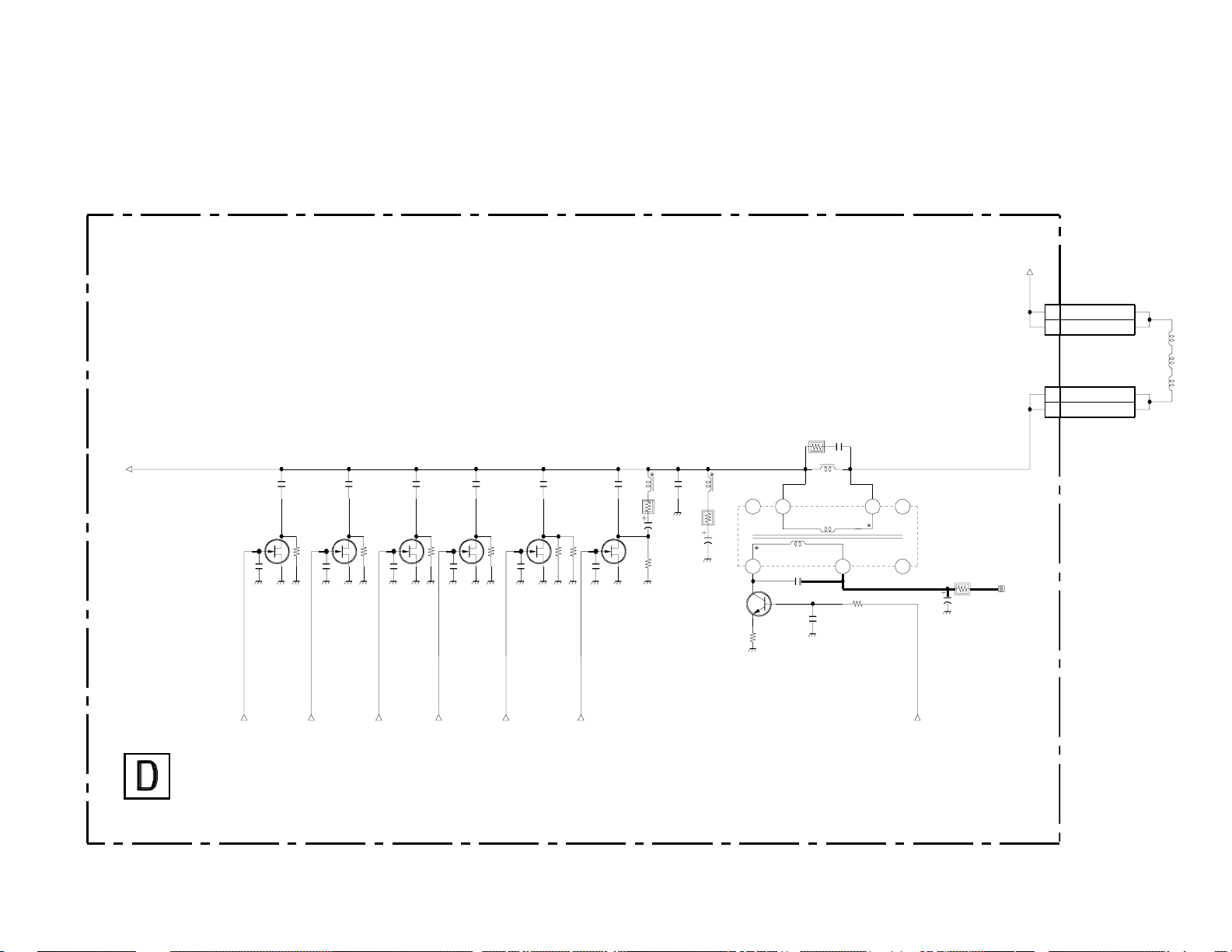
7. Protection Circuitry Overview
Overview
The 19D98 chassis was developed with protection circuits other than HV/ABL.These protection circuits are controlled by
the N board mounted Microprocessor(IC1001);
- B+ Shutdown: Activates when the secondary of the power supply is overloaded.
- S Cap Switch Shutdown: Activates when any of S-Cap Switching FETs are broken.
- V Scan Shutdown: Activates when Vertical Deflection signal is absent or of insufficient level or of a distorted nature.
- H Scan Shutdown: Activates when Horizontal Deflection signal is absent or of insufficient level or of a distorted nature.
Troubleshooting Hints
B+ Shutdown
Refer to POWER SUPPLY section.
S Cap Switch Shutdown
In the event of failure of any S-Cap Switching FETs, and Remote or AC Power switch was turned Off/On, the Microprocessor detects FET gate damage and goes into shutdown mode. For these conditions, refer to the section of H Linearity
Circuit.
Vertical Scan Shutdown
If the V FBP feedback at pin #42 the Microprocessor becomes less than +2.5V, a Shutdown will be initiated. Power Supply
problems may also produce a similar type failure. For these conditions, refer to the V Deflection Circuit or the Power
Supply section.
Horizontal Scan Shutdown
If the H FBP feedback at pin #32 of the Microprocessor becomes lower than +2.5V, Shutdown will be initiated. Some
power Supply problems may also produce a similar type failure. For these conditions, refer to the H Deflection Circuit or
Power Supply sections.
- 18 -
Page 19

180V-2
HV REG DRIVE
PIN# 18 IC805
D901
C921R910
R901
Q901
B+ CHOPPER HV
S
D902
T902
R920
R919
L902
C923
1
FB903
FB902
D903
Q902
HV OUT
C933
C934
R812C802
- 19 -
HV DRIVE PIN# 19
IC805
R911
G2 (1KV)
R811
C801
D908
HV DET PIN# 24
CN801
TO CN510
D906
R922
FB904
S
R921
3
C922
R918
300V
D905
C931
R917
C924
4
1
2
5
7
9
10
8
6
T901
:FBT
HV
17
13
SG901
FV1
14
15
16
FV2
D904
11
C925
R906
C926
SG902
SG903
C930
ANODE OF CRT
R907
CRT VIA
RED FV LEAD
R908
R909
CRT VIA
BLK FV LEAD
C929
R913
R902
R903
RV904
H DF OUT
V DF OUT
D909
C927
R923
R810
12V
C829
IC805 PIN# 12
"HV FEEDBACK"
BOARD
19 D98 CHASSIS HV/PROTECTOR CIRCUIT
C919
R915
R914
ABL DET PIN# 1
CN801
12
Page 20

8. Vertical Deflection (D/N Boards) Circuit
Theory of Operation
The Vertical Deflection block takes its input from the N-board via pins 13 (VSAWN) and 15 (DCC2). These two signals are
generated by the DSP (IC1002) and are both centered on 1.5V. VSAWN is a sawtooth waveform that controls VSIZE. DCC2
is a DC reference that is compared to VSAWN at IC401. VCENTER is controlled by the shift of VSAWN relative to DCC2.
VSAWN and DCC2 are filtered heavily on the N-board by R1035, R1036, C1009 and C1010 and therefore require the use of
IC1007 as a buffer. Along with a buffer a retrace switch is also necessary to short R1036 and remove the filtering during the
retrace. The retrace switch is internal to the DSP and is found between pins 63 and 64 (see schematic on the following page).
IC401 serves as a transconductance amplifier (it amplifies a low level voltage into a high level current) for VSAWN and the
DC difference between VSAWN and DCC2. The current generated by IC401 is fed to the Vertical Deflection Coil. At the
return point of the Vertical Deflection Coil the current flows through R405 and R403 which generates a voltage across them
which is fed back to the amplifier via R404.
The Vertical Deflection Coil has a large inductance (3mH) and therefore it is very difficult to make large quick changes in the
current without high voltage. This situation occurs during the retrace time (+/-15V is not enough). A circuit internal to IC401
is used to raise the voltage at its output. This circuit works as a charge pump that generates about 40V at pin 6 during retrace
and this is added to +/-15V to generate a total of 55Vpk-pk at the output of IC401. Two external components are used for the
flyback generator. C403 is used as part of the charge pump, while D401 is used to block the high voltage of the flyback pulse
during retrace.
VFB Signal Generation
For D98 VFB is a DC signal. It is generated by rectifying the flyback pulse generated at pin 3. D405 and C409 do the
rectification while R417 and R418 the DC level appropriately. If the flyback generation at IC401 does not work (ie. IC401
malfunctions) then the DC level at this point will be reduced and trigger the Vertical Shutdown Protection Mode after one
second the set’s LED will blink amber for 1.5 sec. and then off for 0.5 sec. This is the indication of a scan failure.
Troubleshooting Hints
Vertical Scan Failure
The first step is to check the shutdown log of the monitor and make sure the microprocessor has detected a loss of VFB.
Once this has been verified the output of IC401 should be checked. If a normal output exists after the remote on/off bit is
turned on but the monitor still shuts down then the VFB detection circuit (see VFB signal generation section) is malfunctioning. If no output exists signal tracing should begin at IC1002 pin 1 for VSAWN and pin 2 for DCC2. In shutdown
mode both of these levels should be 1.5V DC. If the remote on/off bit is turned on a sawtooth waveform of about 1Vpk-pk
should appear on VSAWN while DCC2 stays at 1.5V this should last about 2 seconds until a loss of VFB is detected and
the monitor shuts down again. If these signals are good check for the same signals at the output of the N-Board pins 13
(VSAWN) and 15 (DCC2) by repeating the remote on/off step. If no signal is present the problem is with IC1007, if
present continue tracing to R410 and R406. If the signals make it this far the problem is likely in the IC401 area.
IC401
4567123
D401
R407
C403
D405
C409
R417
R416
V.FBP
R418
- 20 -
Page 21

IC401
V-DY througt CN510
- 21 -
RL
R405R403
C403 D401
3
Flyback Generator
TDA8177
5417
R402
LVDY
C402
R401
-16V
R404
C406
D-BOARD
62
+
V+
V-
-
C401
0
+16V
C404
63
+
+
/
-
0
-
64
R409 R1053 R1061
IC1007/1A
+5V
V+
+
R1042
V-
-
R1036
C1010
VSAWN
1
0
IC1002(DSP)
DCC2
2
R410
R1052
R1068
R1081
IC1007/2A
+5V
0
+
V+
V-
C1009
0
0
N-BOARD
0
R1082
R1054
0
Page 22

Heater and Focus Voltages
from D Board
Rear Input
Video
Select,RGB
Process
D/A Conv
OSD Generation
Timing Analysis
A/D Conv
2
I
DDC2Bi
Rear
Input
DDC2B
Front
input
DDC2Bi to N Board
Front Input
Syncs to N Board
C Communication
H Sync,V Sync and H fly
DDC
19 D98 Chassis A board Block Diagram
VIDEO "A" BOARD ELECTRICAL CIRCUIT
RGB Cathode Drv
D/A Level
Active
Video
for ASC
Beam
Current
Feedback
Cuttoff
Voltage
J001
G2 Voltage
G2,Cutoff
and Beam
Current
Feedback
CRT
The main function of the A Board is to receive incoming video signals and process them into the RGB video drives necessary
for the CRT cathodes. Video signals can be received from two sources: One is the conventional 15 D-sub connector and the
second is an additional input located at the front of the monitor consis ing of the female portion of the 15 D-sub. The purpose
of this second input is to allow easy hookup to a laptop computer with the aid of an additional video cable (provided).
The A board circuitry also buffers the Sync timing signals, and provides On Screen Display (OSD) video. The timing
analysis for the Auto Size Center function as well as the Analog to Digital conversion for the Color Restoration functions are
processed on the A-board also. Additional functionality’s include: the Display Data Channel information functions to the
DDC equipped host computer and all the CRT cathodes operating voltages such as the heater, G2 and focus are either
processed or passed to the CRT socket (J001).
A Board Functions
The A Board functions are divided into four operational sections which are described as follows.
1) Video Select and RGB Process Functions
- Video input selecting is controlled by Microprocessor.
- Sync Timing Buffering.
- RGB video signal amplification and adjustment according to white balance requirements, contrast and
brightness settings.
- On Screen Display mixing.
- D/A conversion for RGB CRT cathode cutoff G2 levels control.
2) On Screen Display Generator, Timing Analysis and A/D Conversion
- OSD RGB video pattern generation.
- Timing analysis for Auto Size Center function.
- Analog to Digital Conversion for Color Restoration function.
- 22 -
Page 23

3) G2 and Beam Current Sensing Functions
- Amplifies setup levels provided by Preamplifier A/D outputs for G2 control.
- Beam Current Feedback (BCF) sensing for Color Restoration function.
4) Display Data Channel Interface
- DDC2Bi
- DDC2B
1. RGB Signal Processing (A Board)
RGB Signal Select
The Video and Sync inputs from the rear D sub and front input connectors are applied to the inputs of IC008. Each input is
terminated by an 82 Ohm resistor which is seen as 75 Ohm termination due to effect of the input impedance of IC008. IC008
switches between inputs, at the user’s discretion, when the input select button on the front panel is accessed. A low on IC008
Pin (9) selects the rear D sub input. Sync timing signals are buffered by IC008 before being sent to the N board. Sync on
Green timings are passed to IC001 where the sync signal is isolated and then sent to the N Board.
RGB Signal Amplifiers
Selected and buffered RGB video signals are amplified by IC001. Here the individual Sub Contrasts, Brightness offsets, and
Contrast gain levels are set by the Microprocessor via I2 C control. The OSD RGB video signals from IC003 are mixed into
the main video channels inside IC001. IC002 provides a final amplifier stage for the RGB video signals. This video driver
is internally set to a gain of –14. Therefore at the output pins of IC002 (Pin1, 3 & 5) the waveform is inverted with typical
drives levels on the order of 45Vpp. The Video Driver IC002 drives the CRT cathodes via AC coupling.
RGB Cathode Cutoff Amplifiers
The Red cathode DC cutoff level is amplified by IC004. It is controlled by the D/A output of IC001. The Red cutoff level is
Video Select and RGB Process Functions
+12V
+5V
IC008
R1
R2
G1
G2
B1
B2
V1
V2
H1
H2
SW
Sync Processi ng Circuit
Logic Sync BufferIC006
27
30
35
21
22
To N Board
2
I
2
I
CLK
BPCLP
R OSD
G OSD
B OSD
OSD BLK
10
5
6
C
C
H Sync
V Sync
C Sync
+5V
IC001
228
11
18
12
14
13
17
20
9
24
7
27
1
2
3
4
5
6
30
8
9
D/A G2 Control
4
C105
R
G
B
Cutoff Circui t
R107
R105
IC004
4
9
V-
V+
+
R116
+12V
R108
R122
+80V
IC003
610
D104
R119
R120
D108
D120
C106
C206
C306
+B
D106
D206
D306
R115
C108
+B +B
R219
R220
CRT
R316
R320
8
5
9
3
1
11
Video
Driver
7
10
13
C121
- 23 -
To IC003 A/D
Converters
Green and Blu e
Beam Current Se nsi ng Ci rcui t
Page 24

clamped by discharging C106 via D106. The Green and Blue cathode Cutoff levels are clamped in a similar fashion. The
individual cathode cutoff levels are set for white balance by the Microprocessor via I2C communication with IC001.
Troubleshooting Hints
1) If the screen is blank with no output check:
- Video signals with proper cutoff levels are provided to the CRT cathodes.
- Supply voltages are at the appropriate levels and locations starting at CN305.
- Heater voltage is correct and present at the heater cathode.
- Diode shorts at the cathodes.
- Sync timing signals are present at the output of IC008.
- That there is I2C communication to IC001.
2) If the screen is lighted with no video check:
- Control, blanking and clamp signals to IC001, IC002, and IC008.
- +5V, +12V, and +80V to these circuits.
-For shorted diodes on the IC002 outputs.
3) If colors are wrong or missing and white balance cannot be adjusted check:
- Each individual color signal path comparing DC offset and peak to peak signal levels to each other to determine if
there is any single amplifier at fault.
- For shorted diodes on the IC002 outputs.
2. On Screen Display Functions
On Screen Display(OSD)
IC003 is the On Screen Display character and graphic generator. It provides RGB and Fast Blanking data to IC001 for
mixing with the main video channels when required. Outputs voltages are two dimensional, either 0V or 3.6V. IC003 is
controlled by the Microprocessor via the I2C bus. The sync timings necessary are V sync and H Fly. The reference oscillator is set by an 8MHz crystal X001.
Timing Analysis
Timing Analysis for the Auto Size Center function is provided by IC003. Time measurements are taken with V sync (pin6),
H sync (pin5) and Active Video (pin7). These measurements are then sent to the Microprocessor via I2C communication for
size and centering calculations.
A/D Conversion for Color Restoration
Coloration can be achieved by measuring the CRT beam current during the blanking time. This current is converted to a
voltage via a sensing circuit. This voltage is converted to a digital format by the Analog to Digital converters contained in
IC003. There are three A/D converters for the RGB beam current feedback (BCF) circuits. These digital representations of
the RGB beam currents are stored in the BCF Red, BCF Green, and BCF Blue registers at the time white balance is finished
on the production line. In the field the Color Restoration can be achieved by sampling the RGB beam currents again and
comparing these new values to the ones stored in the BCF registers. The Microprocessor then adjusts the cutoff voltages
until the measured beam current is equal with the values stored in the BCF registers. This function is not done automatically.
It is necessary for the end user to activate this function through the OSD menu from the front panel controls.
Troubleshooting Hints
1) No OSD is displayed, check:
- RGB and Fast Blanking inputs to IC001. If there are no signals then IC003 may be at fault.
- That +5V is supplied to IC003(Note: Pin 18 will read 3.6V)
- V Sync and H fly signals are at pins 4 and 7 of IC003 respectfully.
- That Crystal X001 is oscillating (8MHz).
- That there is I2C communication to IC003.
2) Auto Size Center Does is not working, check:
- That +5V is supplied to IC003.
- V Sync, H Sync, H fly, and Active Video signals are at pins 6, 5, 7 & 8 of IC003 respectively.
- That Crystal X001 is oscillating (8MHz).
- That there is I2C communication to IC003.
- 24 -
Page 25

From N
Board
To
IC001
D024
ASC
Measurement
R080
C106
Active
Video
From
IC001
Timing
Analysis
Display
Controller
IC003
5V
Regulator
IC009
PLL
Oscill
ator
Cutoff
Control
D/A from
IC001
Beam Current
Measurement
Beam
Current
A/D
2
IC
Interface
Same as R
channel
C037
From N
Board
R003
Red
Green
Blue
C038
Cutoff Circuit
R107
C105
Simillar to
Red Channel
R105
+80V
+12V
IC003
610
D104
8
9
11
Video
Driver
IC004
4
9
V-
V+
+
R116
7
10
13
R108
C121
R122
Beam Current Sensing Circuit
C106
5
3
1
R119
R120
D108
D120
C206
C306
+B
D106
D206
D306
R115
C108
+B +B
R219
R220
CRT
R316
R320
3) Color Restoration doesn’t work. Bad color after restoration, check:
- That the OSD is working. If not follow steps of 1).
- BCF registers on the Color Table. Look to see if any registers are abnormally low or high.
The following are typical ranges:
Mode 1 Mode 2 Mode 3
R BCF 110~140 130~160 105~135
G BCF 115~145 90~120 130~160
B BCF 125~155 45~80 180~230
If values seem strange, check voltages at the BCF pins (20,21,22) of IC003. With a full white image the voltage should be
around 2.5~4.5V. If levels seem strange check beam current sensing circuit (next section).
3. G2 and Beam Current Sensing
G2 Amplifier
The G2 reference is provided to IC005 Pin 5 by the IC001 D/A converter. The G2 voltage at the cathode is typically 500v ~
750V.
Beam Current Sensing Circuit
Sensing resistors R108, R208, and R308 convert the beam current flowing through the cutoff amplifier during the blanking
time into a voltage. This voltage is then AC coupled and clamped to ground. It is then rectified to a DC voltage and sent to
the A/D converters of IC003. Here it is converted to digital format and stored in the RGB BCF registers.
Troubleshooting Hints
1) If picture is black, check:
- G2 level at the cathode using HV probe.
- Input to G2 amp, Pin 5 of IC005.
- 25 -
Page 26

Cutoff
Control
D/A from
IC001
To IC003 A/D Converter
Range
1V-4V
Red
Green
Blue
Cutoff Circuit
C105
Similar to
Red
Channel
R107
R105
Beam Current Sensing Circuit
D104
C106
C206
C306
Video
Driver
IC004
2
4
6
9
V-
-
11
12
V+
+
2
13
R108
R116
R122
D105
R119
R120
5
7
10
13
6
Beam Current Sensing Circuit
C121
D120
D108
C108
D106
D206
D306
R115
+B +B
R219
R220
R316
R320
Range 1V-4V
G2 Control Circuit
R048
R049
R047
13
5
V+
3
V-
6
2
12
11
IC005
CRT
Range 400V-800V
R053
R048R064
D045
Q1
R045
C048
R31
From IC001 D/A Converter
- Heater voltage at the cathode.
-+12V, +5V, and G2 voltage coming from D board.
2) Color Restoration doesn’t work. Bad color after restoration, check:
- Check waveforms at pins 6, 11 and 14 of IC004.
- Trace these signals through the rectifier back to IC003.
- If there are no waveforms at pins 6,11, and 14 then IC004 may be suspect.
4. Display Data Channel Circuits (DDC)
This display can support two video sources. The front input supports DDC2B. While the rear input supports DDC2Bi. For
DDC2B (Front Cable) IC007 is a serial memory device providing Extended Display Identification or EDID data that is read
by the compatible Host Computer on Pin 5. The basic EDID format consist of 128 bytes which are described in the table
below. The 15 Pin VGA connector allocation is also described. The compatible Host Computer provides a V CLK on Pin 7
that is derived from the V Sync input and is used to set the timing of each data reading cycle. The data is clocked by the
input of IC007 Pin 6. The rear input supports DDC2Bi. The data is passed through the A Board to the Microprocessor on the
N Board via CN311.
Troubleshooting Hints
1. The DDCB circuit should be checked if error DDC messages or erroneous monitor identification data is indicated by
DDC2B the compliant Host Computer. Check that the V CLK and S CLK signals are input to IC007 on Pins 7 and 6. The
Data transition should be visible at Pin 5.
- 26 -
Page 27

DDC Data format and VGA Connector Allocations
Basic EDID consist of 128 bytes 15 pin VGA type connector
Number Description Pin No Assignment Pin No Assignment
8 Bytes Header 1 RED Video 11 Option
10 Bytes Vender/Product Identification 2 GREEN Video 1 2 Data(SDA)
2 Bytes EDID Version/Revision 3 BLUE Video 1 3 H SYNC
5 Bytes Basic Display Parameters/Features 4 Option 1 4 V SYNC
10 Bytes Color Characteristics 5 Return 15 Clock(SCL)
3 Bytes Established Timings 6 Red Return
16 Bytes Standard Timings 7 Green Return
72 Bytes Detailed Timing Description 8 Blue Return
1 Bytes Extension Flag 9 Option +5V
1 Bytes Checksum 10 Sync Return
Display Data Channel Circuits (DDC)
DDCSLC
DDCSDA
Host GND
To CN306
1
2
3
D012
R92
D013
D011
R77
D010
IC007
DDC28
Cable
V Sync From Front Input
Front
D018
Host GND
4
DDC SDA
3
DDC SCL
2
D007
1
DDC2Bi(Rear Cable)
NC
D006
D005
1
3
2
To N Board
4
- 27 -
Page 28

N BOARD SYNC AND CONTROL CIRCUITS
Overview
The N board performs H and V Sync processing within the Microprocessor (IC1001)and DSP (IC1002 Digital Signal
Processor) which generates shaping, centering, deflection drive pulse and other corrections. The DSP is controlled by the
Microprocessor using I2C BUS with the Microprocessor having an external EEP ROM. Other Video functions are controlled
by Microprocessor through the I2C bus.
MICROPROCESSOR
H Sync (sync out from Microprocessor) and V sync (sync out from Microprocessor) is buffered by internal sync processors
and will be sent to DSP and OSD (on A board). In the absence of Video Input, this output will be the Microprocessor’s free
running output. The Microprocessor directly outputs the control of H center, H Lin Balance, and Rotation by DAC outputs. In
Accordance with the monitor’s operating condition, it switches the Remote On/Off, Heater On/Off, Input select, S Caps, and
Degauss.
DSP (Digital Signal Processor)
This IC requires 3.3v VDD. The 3.3vdc is supplied from IC1006 (Regulator). The DSP outputs waveforms for the deflection
circuit with most of these going to D Board. Pin #1 is V SAW output and will go to D board through IC1007 acting as a
buffer. Pins#6 and #7 are for Dynamic Convergence. Pins #60, 61 are for Static Convergence. Pin #10 is H DF output and
#58 is V DF. Pin #59 is V Key output and #64 is H Shape. Pin #57 is PIN/KEY Bal out, this is supplied to the Phase Lock
Loop(PLL) Circuit of the DSP which is on pin#12 – 22. H Drive Pulse will be outputted from pin#25 after being modulated
by Bal correction and Moire correction(#22). This IC works with 3.3v VDD. The 3.3v is supplied from the IC1006 (Regulator)
Trouble Shooting Hints
See attached “FLOW CHART” to confirm N Board issues.
Incorrect/No Wave form from DSP
Check the 3.3vdc from IC1006, if O.K, confirm that I2C BUS is sending a pulse(0v-5v) to the DSP. Confirm that Reset
(pin#49) is HI and POC-IN(pin#30) is almost 1v.
No Communication or Microprocessor related failur e
Check CN1003, CN1004 connections first. If OK, then check 5v supply and to see if X1001 is oscillating, also
RESET(pin#54) is HI. In case of No Communication, confirm pin #38(RXD) is receiving pulse signal (0v-5v).
From A boad
H Sync in
V Sync in
HFDP
KEY SCAN
TXD/RXD
ABL
HVDET
C Sync in
IN PUT SW
REMOTE
DEGAUSS
HEATER
-S1
-S2
-S3
IC1001
MICRO
H CENT
ROTATION
H LIN BAL
IC1005
EEPROM
I2 C BUS
H SYNC OUT
V SYNC OUT
RESET
IC1003
RESET
XSC/YSC
XDC/YDC
HDF/VDF
H SHAP
V Key
HD
IC002
DSP
DCC
2
C BLANC
3.3V
V SAW
IC1007
BUFFER
N board
IC1006
DSP
5V
- 28 -
Page 29

System Block Diagram
IN VIDEO X2
IN SYNC X2
DISPLAY DATA COMMUNICATION BUS
(DDC)
HEATER
MAIN
AC
POWER SW
POWER SUPPLY
JIG
I/O(RS232C)
D BOARD
DC POWER
2
I
C-BUS
Deflection
PS Mode
VIDEO BLOCK
ASC Measurement
1Kv
SYNC PROC.&
CONTROL
N-BOARD
OSD
A-BOARD
Sync
FOCUS
BLOCK
FBT
I/O
RGB VIDEO
FOCUS/G2
STATIC/
DYNAMIC
FOCUS
H & V
DEFLECTI
I/O
ON
HV
D.CONV
H/V
DEF.
TILT
USER
CONT
H
BOARD
Alignment jig
(factory,service)
PC
(Host computer)
DIGITAL CONTROL COMMUNICATION DIAGRAM
HV sync
Micro
DDC
processor
IC1001
User conrol/
Power sw
2
I
C-BUS
VIDEO BOARD
A BOARD
DSP IC
IC002
EEPROM
Pre-AMP
IC001
OSD
IC003
BIAS
DRIVE
CONTRAST
BRIGHT
G2
Information for USER
SIZE(ZOOM)
CENT
GEOM(PIN,KEY.x)
CONV.(STAT,DYNAMIC)
FOCUS
N BOARD
- 29 -
Page 30

GENERAL TROUBLESHOOTING
Input crosshatch signal at prime
Mode 94KHz X 70 Hz
No Picture A
Missing Color or Abnormal Color
Visible Retrace or Visible Raster
Mis-convergence
Poor Focus
Unsynchronized Image
B
C
D
E
F
Abnormal Geometry
Abnormal Image Size
Shutdown I
No Communication
- 30 -
G
H
J
Page 31

NO PICTURE
A
Is amber
Power LED
Blinking?
No
Is
amber LED steady on?
No
Is green power LED On?
Yes
Does
A-Board make proper
contact with CRT gun?
Yes
Yes
No
No
Yes
I
(See Part Level Board Repair Section)
Check the video cable connection or
INPUT SELECT registers
Is Monitor beeping? (Small)
No
Press power switch, if LED does no turn on,
repair"power supply"
Carefully press A Board
to make proper contact with CRT gun
1
Yes
Repair Video circuit
or repair H deflection
12
2
Check heater, G2, red, green and blue cathode
voltage levels.
Repair Video if needed
12
Done
No
- 31 -
Can you get picture?
Yes
Page 32

MISSING COLOR
B
Yes
Check signal generator & cable
I
(See Parts Level Board Repair Section)
No
Yes
Are proper video
levels present
on CN307,on313
pin 2, 4 &6?
Yes
Is amber
Power LED
Blinking?
No
12
(See Parts Level Board Repair Section)
- 32 -
Page 33

VISIBLE RETRACE
C
Yes
Check white balance
adjustment and check "H
Blank" register value.
Check IC004, IC005,G2
control circuit. IC001
pin 6 and FBT
Check connections &
signal at CN309 pin 1I
Check CN309 Pin 3
3
No
No
No
Is G2 voltage correct?
Yes
Is
blanking pulse present on pin18
of IC001 on A-Board?
Yes
Is blanking
pedestal present in the
waveforms at pin 12 of
IC001?
Yes
Check IC002 and IC004
No
blanking pulse present on all
Is
cathodes?
Yes
Done
- 33 -
Page 34

MISCONVERGENCE
D
Reset and check,
Try adjusting convergence
using front panel controls
Yes
Try adjusting convergence
using DAS
Is the convergence
within spec ?
No
No
Is the convergence
now within spec?
Check the convergence
circuit(IC701,704)
Change DY and
readjust convergence
Is the convergence
within spec
now?
Yes
Yes
Done
Is the convergence
circuit(IC701,704)
OK ?
No
Repair &
adjust
B
Yes
No
Change CRT &
readjust
conergence
Done
- 34 -
Page 35

POOR FOCUS
E
Adjust focus
VRs on FBT
Age monitor and
check for focus
change
6
Yes
Improved
focus?
No
Check focus leads
from FBT to CRT
socket
Check video bond CRT
socket
No
Is dynamic focus
circuit OK ?
(See Parts Level Board
Repair section)
Yes
Replace CRT
and verify
focus
Done
- 35 -
Page 36

UNSYNCHRONIZED IMAGE
F
Check input
signals CN307 or CN313
pins 4,8 and 9
Check video
cable
Check sync
separation circuits
on video board
Check wire
dressing and
connection
(from N board)
OK but
no
still
syncro
No
No
No
Signals levels
correct?
Yes
Signals at CN309
pin 4, 5 or 7
OK?
Yes
Signals at CN
306 pins1 and
2 OK?
Yes
Check N board
10
Done
- 36 -
Page 37

ABNORMAL GEOMETRIC DISTORTION
G
Down load
factory settings
and readjust
3
(See Parts Level Board
Repair Section)
Does distortion change
a lot when changing to
inverse pattern
No
Identify distortion
problem and repair
(see board level repair)
See"H Deflection circuit"
"H Line/Ringing correction"
Explanation
57
or
No
Is geometric
distortion OK?
Yes
Done
- 37 -
Page 38

5
(See part level board
Repair Section)
4
ABNORMAL IMAGE SIZE
H
With user controls
adjust picture size
No
Does horizontal size
adjustment?
Yes
No
Does vertical size
adjustment ?
(See part level board
Repair Section)
Yes
Adjust monitor
Done
- 38 -
Page 39

Check power
supply
10
SHUT DOWN
I
No
Is amber
LED blinking
Yes
Check shut down
log registers in IC1001
and Repair refering to
the explanation of
"Shut down"
- 39 -
Page 40

NO COMMUNICATION
J
Yes
Check connections
Check connect settings
and connections
Check Power supply
No
No
No
Are connections
to monitor OK?
Yes
Are computer settings and
connections OK?
Yes
Is 5 volts present
at CN801 pin 43?
Yes
Check N board
10
Done
- 40 -
Yes
Page 41

PARTS LEVEL BOARD REPAIR
Parts Level Board Repair
(1) Power Supply
(2) Horizontal Delection
(3) High Voltage
(4) Vertical Deflection
(5) Horizontal Size
(6) Horizontal Center
(7) Key and Pin
(8) Key and Pin Balance
(9) Rotation
(10) N board
(11) Dynamic Focus
(12) Video
(13) Convergence
- 41 -
Page 42

POWER SUPPLY
1
Check F601
and D601
Check Q505,506,901,
902 and video board
Check
IC701,703,704,604,601,504
R617
Replace Q602,
Check D603,615
R609,615,IC601
Replace parts,
verify voltage
Yes
Yes
No
No
Does power
supply make
chirping noise?
No
Does Power supply
try to start?
No
Q602 OK?
Yes
Are D603,615
R609,615
IC601 OK?
Yes
Check A board by
disconnecting CN602
If OK, replace SRT
Replace IC605,IC805
Check secondary diodes,
FPRD resistors
No
Operating?
Yes
Verify voltages and
adjust monitor
Done
- 42 -
Page 43

HORIZONTAL DEFLECTION
2
Change
IC805
Change
IC805
N board
( )
10
Change Q502,503
Check Q504,
& R504
Check Q506,D503
and R512
No
No
No
No
Is CN801 pin 26
output OK?
(HD OUT)
Yes
Q502 emitter
out put OK?
Yes
Is Q504 Gate
input OK?
Yes
Is Q506 drain
output OK?
Check R507,Q504
Change T501
No
Yes
Is Q504 drain
output OK?
Yes
Change
Q505
and T501
Done
- 43 -
Page 44

Replace Q902,901and
D901
10
HIGH VOLTAGE
3
No
Is Q902,901
OK?
Yes
Check R910,D901 and
change IC805
Check R911
and replace IC805
Resolder,
if necessary
No
No
No
Is Q901 gate
input OK?
Yes
Is Q902 gate
input OK?
Yes
Is soldering or
mount
around RV904,C926
are OK?
Yes
Change FBT,verify
operation and adjust
monitor
- 44 -
Done
Page 45

Check power
supply
10
VERTICAL DEFLECTION
4
No
Is +15V and
-15V OK?
Yes
Check N board
10
Replace IC401
and check R401
R407,D405
Replace, if necessary
No
No
Is CN801
pin13(VSAW)and
pin15(VREF)
waveform OK?
Yes
Is (-)side of C403
showing 30vp-p
pulse?
Yes
Change DY
Adjust
monitor
Done
- 45 -
Page 46

HORIZONTAL SIZE
5
Check T504 and IC805or
N board
10
10
Replace IC805 and
check N board
10
Check HV
Yes
Is horizontal size
the only problem ?
No
Yes
Distortion
a problem ?
No
No
Vertical size
OK?
Yes
Repair
H-Lin/Ringing
Correction circuit
No
Is H.linearity
OK?
Yes
Replace DY
and readjust
Done
- 46 -
Page 47

HORIZONTAL CENTER
6
Check landing
and if it is OK,
Check H centering
10
circuit
Check Q514
and D506
No
Is Raster center
OK ?
Yes
Is blanking pulse
(CN309 pin1)
OK ?
Yes
No
Is Q514 emitter
output OK?
Yes
Check N board
10
- 47 -
Page 48

Check N
board
10
10
KEY AND PIN
7
No
CN801 pin27
outputs normal?
Yes
Check Power
supply
1
N
o
Is B+ voltage
OK?
Yes
Check T504,IC805
and related
components
Done
- 48 -
Page 49

Check Rotation
10
circuit/adjustment
KEY AND PIN BALANCE
8
No
Is
Rotation OK?
Yes
Check N board
10
- 49 -
Page 50

ROTATION
9
Check N
board
10
10
Connect
CN702
Replace
IC702
No
No
No
Is
CN801
pin40 OK?
Yes
Is
CN702 properly
connected?
Ye
Is
IC702 pin4
output OK?
Ye
Check RV709 FPRD
OK
s
s
Replace
DY
Done
- 50 -
Page 51

N BOARD
Check the connection
between D and
N board
10
OK
Check soldering
of IC1006
or Replace
10
Check
IC1001,1005
No
No
Is
3.3V+/-0.1V
present on +side of
C1014?
Yes
Is
2
I
C BUS LINE
(CN1003 pin5,7)
has plus
communication ?
Yes
Check for solder
bridge, crack
or any mount mistakes
OK
Change
N board
- 51 -
Page 52

DYNAMIC FOCUS
11
Check Focus leads
are not reversed
Check N board
10
Replace IC703 and
R742
Replace T701,Q706
No
No
Is CN801 pin 33
output normal?*
(V.Focus)
* Should be less than
1.6vp-p
Yes
Is
IC703 pin 6 output
normal?
Yes
Is
FBT pin14,15
waveform OK?
Yes
- 52 -
Change FBT
Done
Page 53

Check connector
CN309
10
and IC003
VIDEO - A BOARD
12
OK
No
Check if I2C bus
pins
(CN309 pin6.8)
Yes
Check IC001
and IC003
Replace parts
& Verify
Check IC004
and +B
No
No
No
Check
IC001 pins 20
24 and 27
Yes
Check
IC002 pin 1,3,
and 5 OK?
Yes
Are cathode
DC levels and
waveforms
Correct?
Yes
Check IC005
G2 control circuit
and FBT
No
Is G2 voltage
correct?
Yes
Change CRT
Done
- 53 -
Page 54

Correct harness
and change IC704
10
R718, 750
Change to
Convergence SW
Register to 3
and
readjust as required.
CONVERGENCE
13
OK
No
Check if harness for
CN701 is not
switched at DY
connection
OK
NG
Check "CONV SW"
registers
OK
Still No Good
Change
DY
Check all RS
resistors
Change
IC701, 70
4
Readjust and
Done
OK
OK
- 54 -
Page 55

NOTES:
- 55 -
Page 56

9-978-848-01
Sony Corporation
Sony Technology Center
Product Quality Division
Service Promotion Department
- 57 -
English
99AJ74253-1
Printed in U.S.A.
© 1999.1
 Loading...