

Page 1
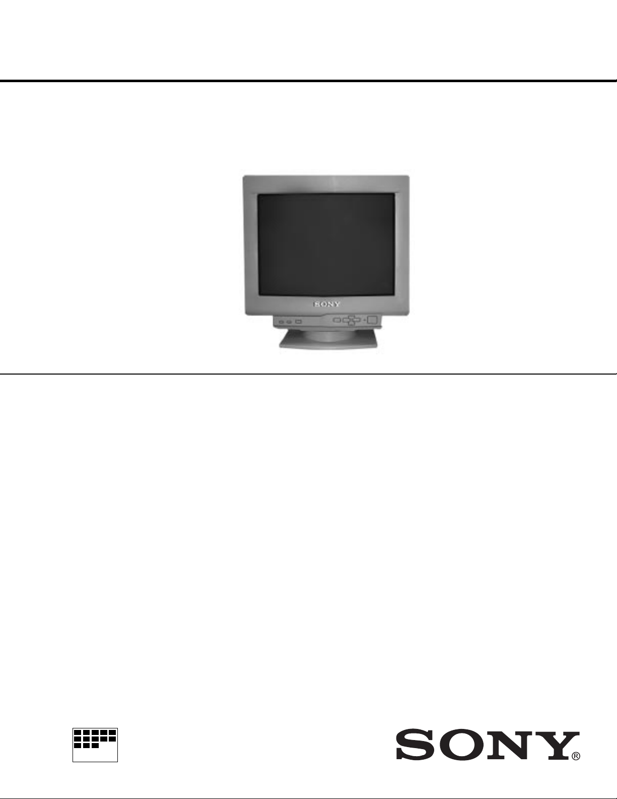
D1H
OPERATION MANUAL
TROUBLESHOOTING MANUAL
CHASSIS
TABLE OF CONTENTS
CIRCUIT DESCRIPTION
D Board (Power Supply Section) ........................ 2
D Board (Deflection Section) .............................. 2
A Board ............................................................... 3
TROUBLESHOOTING ........................................... 4
PARTS LEVEL BOARD REPAIR ........................... 15
TRINITRON® COLOR COMPUTER DISPLAY
MICROFILM
- 1 -
Page 2

CIRCUIT DESCRIPTION
D Board (Power Supply Section)
1. AC Input Section:
The AC input section is designed to accept the incoming AC
voltage in range of 100 V- 240 V AC and filter out noise that
could be conducted back into the mains. This is done by a
combination of capacitors (C601 & C608) and the line filter
transformer(LF 602). D601 full wave rectifies the AC input
voltage. Peak inrush current is limited by a thermistor
(TH600), and a resistor (R600).
2. Degauss Circuit:
During power up the CPU (IC 901), turns on Relay (RY601),
to allow current to flow into the degaussing coil through the
posistor (TH601), when the power switch is on. The CPU
shuts off R Y601 approximately 5-6 seconds after power-up.
3. Primary Section (Flyback type):
The essence of the primary section is the power controller IC
(IC601). Key pins are:
Pin 1: This pin is Vcc. Normal value for Vcc is 15.0 V.
During power-up the chip is powered via a kick-start resistor
(R610) until the secondary supply is avilable from T601.
Pin 3: Outputs the drive pulse for the main switching transistor Q602.
Pin 5: If the power supply load becomes high enough to
drop the voltage below 1 V(when Vcc<13 V) then IC 601
automatically limits the output duty cycle to limit the output
power.
Pin 6: If the voltage on this pin exceeds 17V the power supply shuts off and can only be restarted by disconnecting and
reonnecting the AC line.
Pin 7: If the voltage on this pin (primary current feedback)
exceeds 1 V the power supply will cycle-by-cycle current
limit to keep this voltage below 1 V.
Pin 8: Provides feedback to ensure that the power operates
in the discontinuous mode by checking for evidence of residual magnetism on the secondary winding. This is done by
verifying that there is zero voltage during the dead-time.
Pin 10 & 16: The power supply switching frequency is
preset to 70kHz by C614 connected to pin 10 and by R611
connected to pin 16.
Pin 11: The soft start capacitor (C616) connected to this pin
eliminate potentially destructive voltage transients during
start-up.
4. Secondary Section:
The secondary voltages are 185V(B+), 80V, 15V, -15V, +8V
and -8V . An external error amplifier IC is used (IC604) to
regulate the 185V line by keeping the voltage divider of R628
and R630 at 2.5 V. During standby mode current source Q604
turns Off and lowers all the secondary voltages by approximately 80%. The CPU shuts off the filament by turning off
Q605 and Q606 during the DPMS “off-state”.
T r oubleshooting Hint: Power supply will not operate with
the A Board disconnected.
D Board (Deflection Section):
1. Horizontal Deflection Circuit:
The 12Vp-p horizontal drive pulse is generated by the inverter Q903 using the Jungle IC 902 H.out pin 17. A pushpull amplifier (Q501 and Q502) buffers the drive pulse prior
to Q511, which drives the primary winding of the basedrive
transformer (T504).
The secondary of the basedrive transformer drives the base
of the Horizontal Output Transistor(HOT) Q507. When HOT
is turned on current begins to ramp up through the yoke thus
deflecting the beam from the center to the right side of the
screen. When the HOT is turned off the current that is flowing through the yoke ramps down rapidly to zero charging
up the Retrace Capacitors (C518, C521, and C522) to the
peak flyback voltage. This moves the beam back to the center of the screen during the blanking time.
At this point of time the Retrace Capacitors discharge driving the beam to the left side of the screen. When the retrace
capacitors have fully discharged the retrace diode (D506) is
turned on and the yoke current ramps back down to zero
moving the beam from the left to the center of the screen for
the next cycle. The CPU switches Q512, Q513, Q514, Q515
and Q516 on and off in different combination to allow 8 different S-cap values to compensate the horizontal linearity
over the frequency range.
A thermistor (TH501) located near the S-CAP transistors provide a shutdown mechanism in the event of a high thermal
condition in this area of the PCB. The chopper circuit regulates the horizontal size. The Deflection Chopper Circuit
Primary components include Q520(Deflection Chopper Transistor), D516(free-wheeling diode), L503 and IC 501.
2. Vertical Deflection Circuit:
The vertical deflection system utilizes a transconductance
amplifier IC 401. The negative input is driven by V.Saw
signal generated by Jungle IC 902. The positive input of the
- 2 -
Page 3

amplifier is Vref. Signal generated by IC 701(Convergence
IC). In the event of a loss of vertical retrace the horizontal
drive is shutdown and the screen is blanked to protect the
CRT.
3. Dynamic Focus Circuit:
Horizontal Parabola is injected into the secondary side of the
focus transformer(T503). In order to keep the amount of
parabola constant over the horizontal frequency range the
values of the AC coupling capacitors are changed by the transistors, which switch the s-caps. This signal is amplified by
the turns-ratio to the primary side of the transformer. The
primary is modulated at the vertical rate by a common emitter amplifier (Q504).
D Board (HV Regulation Section):
HV Regulation is accomplished by voltage feedback derived
off pin 14 of the flyback (T501). Main circuit components
of HV Circuit are T501(Flyback transformer), IC501(PWM
controller IC), Q503(HV Chopper transistor), and Q510(HV
switching Transistor). Q510 is just a switching transistor with
a fixed duty cycle supported by IC 501. Q503 is HV Chopper transistor and its function is to maintain consistent energy for different conditions, e.g. various picture brightness
or luminance.
D Board (Digital Convergence Section):
The main components of Digital Convergence Circuit are IC
701(Convergence IC), IC 702(Amplifier Hybrid IC), and IC
902(Jungle IC).
A BOARD:
1. Pre-Amplifier:
Preamplifier IC(IC 001) is controlled by IIC bus. It receives
R,G, and B signals from Sharpness IC(IC 006) and gives
amplified output signals up to 3 V p-p value. It provides R,
G, and B drive controls to make proper white balance. It
controls contrast, brightness, and OSD contrast by IIC bus.
Also, it has a blanking mix circuit and OSD mix circuit. When
pin 15 receives high signal(5V) from IC 003, OSD signals
are generated as outputs instead of original video signals.
2. Sync Processing and Sharpness Function:
The main function of IC 006 is sync processing and sharpness. IC 006 adds the sharp edge to R,G, and B signals and is
controlled by pin 12. The sharpness IC 006 includes the Sync
Seperation circuit for Sync on Green signal. The composite
sync (TTL Level) is the output from pin 14.
3. Output/Cutoff Stage:
The outputs of the pre-amp are fed into the LM2405(IC002)
7 ns video output stage where they are amplified up to 40 V
p-p. The output of this stage is AC coupled and DC restored
to the outputs from the cutoff IC(IC 004). The red, green,
and blue cutoffs are adjusted via PWM control signals from
Preamplifier IC 001.
4. G2 Section:
Convergence IC 701 generates the basic signals for Horizontal and Vertical Static and Dynamic convergence. To generate Static convergence outputs (Pins 8 & 9 of convergence
IC 701) the IC 701 uses V.sin signal and V.div. signals both
coming from IC 902(Jungle IC) pins 10 and 27 correspondingly. IC 701 generates dynamic convergence outputs i.e.
H.Conv-out and V.Conv-out (pins 6 & 7 of IC701) using
V.Sin, V.Div. and H.Drive signals all coming from IC
902(Jungle IC).
Convergence Amplifier IC 702 generates the amplified current waveforms for static and dynamic convergence. Basically the IC 702 consists of error amplifier Op-amps which
uses 4 basic convergence output signals (static & dynamic
convergence ouputs from pin 6,7, 8, and 9 of IC 701). IC
702 also uses V.ref (reference voltage) signal coming from
IC 701 for each op-amp. Finally the IC 702 gives four convergence current waveform outputs (static & Dynamic with
both polarity) which controls the convergence performance
of picture.
The G2 section is the regulation circuit consists of an opamp (IC005) regulating a common emitter amplifier Q001.
The G2 is adjusted controlled from Preamplifier IC 001 pin
28(G2). The G2 has an adjustment range of 0 V to 650V.
During any shutdown mode G2 is immediately adjusted down
to 0V to cutoff the beam.
5. OSD (On Screen Display):
OSD IC (IC 003) is controlled by IIC bus. It provides R,G,
and B signals to Preamplifier (IC001) for mixing. Pin 12 of
OSD (IC 003) is used to switch between OSD R,G, and B
signals and original R,G, and B signals. Horizontal and vertical flyback pulses are supplied to OSD IC to determine the
OSD position on the screen.
- 3 -
Page 4

GENERAL TROUBLESHOOTING
- 4 -
Page 5
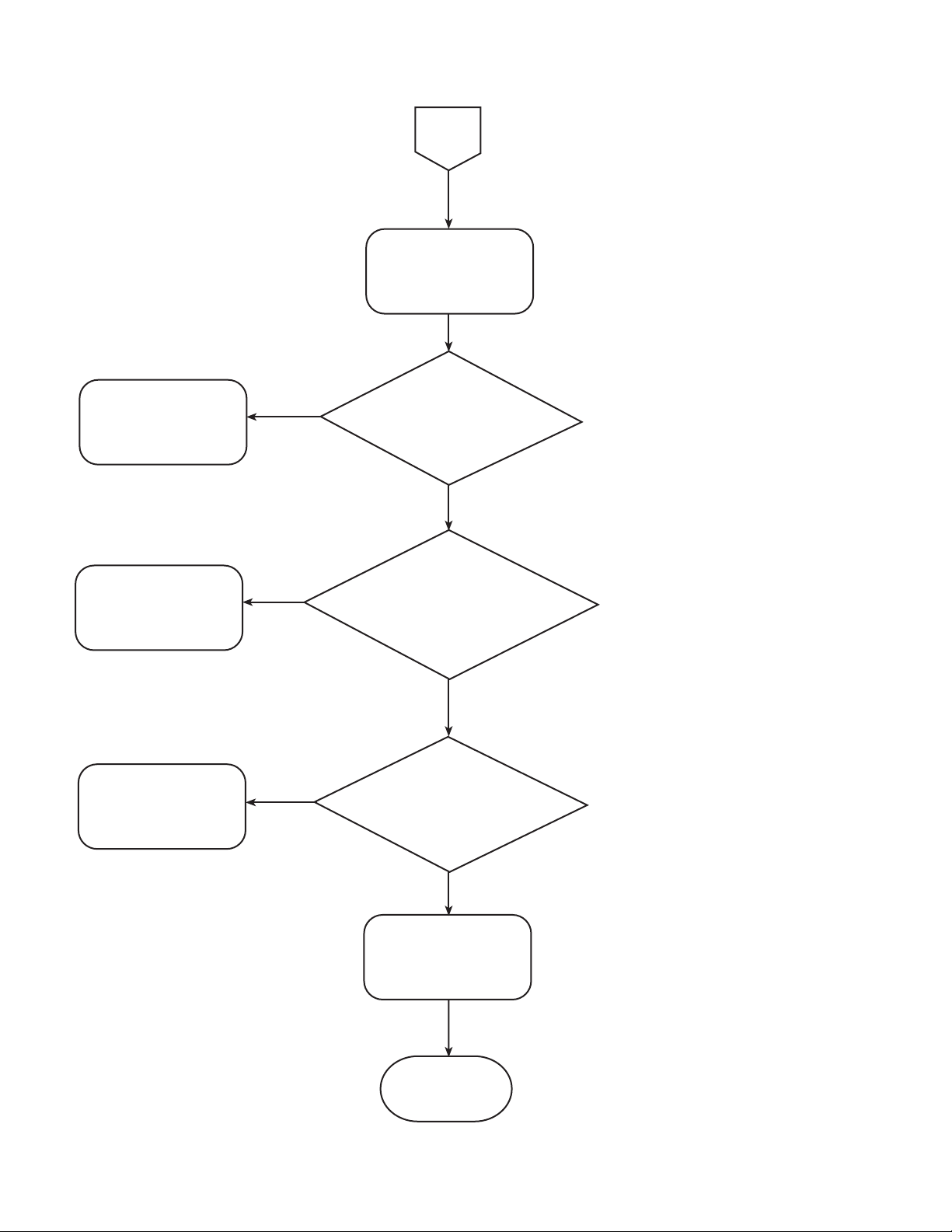
NO PICTURE
A
Is amber
power LED
blinking?
No
Is
amber LED
on?
No
Is
green
power LED
On?
Yes
Yes
I
Yes
Check the video
cable connection
No
Press power switch,
if LED does not turn
on, repair power supply (I)
Does
A-Board make proper
contact with
CRT gun?
Yes
Check heater, G2, red, green
and blue cathode voltage levels.
Repair video (12) if needed
Done
- 5 -
No
Press A Board carefully
to make proper contact with
CRT gun
No
Can
you get
picture?
Yes
Page 6
Check signal
generator &
cable
12
(See Parts Level Board
Repair Section - page 15)
No
No
MISSING COLOR
B
Are
proper video
levels present
on CN 307 pins
2, 4 & 6?
Yes
Are
proper AC
voltages present on
all cathodes?
Check IC004,
IC001 pins 3,
4, 5 and +B
voltage
Check IC005,
G2 control,
circuit, IC001
pin 28 and FBT
No
No
Yes
Are
proper DC
voltages present
on all
cathodes?
Yes
Is
G2 voltage
correct?
Yes
Change the
CRT
Done
- 6 -
Page 7

Check IC005,
G2 control
circuit, IC001
pin 28 and
FBT
No
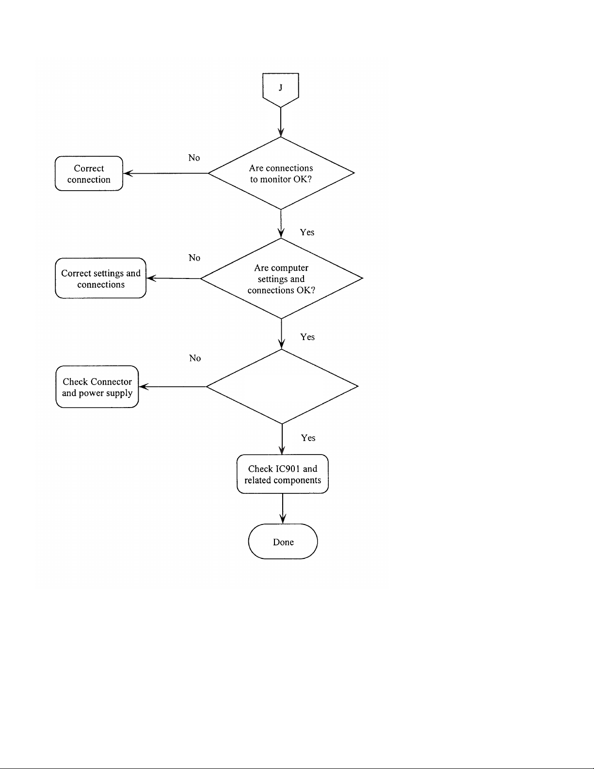
VISIBLE RETRACE
C
Check white balance
adjustment
Is
G2 voltage
correct?
Yes
Check
connections &
signal at
IC901 pin
46
Check IC001
and related
components
Check IC002
and
IC004
No
No
No
Is
blanking pulse
present on pin 16 of
IC001 on A-Board?
Yes
Is
blanking pedestal
present in the waveforms
at pins 18, 22 &
25 of IC001?
Yes
Is
blanking pulse
present on all
cathodes?
- 7 -
Yes
Done
Page 8
Try adjusting convergence
using DAS
MISCONVERGENCE
D
Reset using
front panel control
Try adjusting convergence
using front panel controls
Is
No
the
convergence now
within spec?
Yes
Done
Yes
Is the convergence
within spec?
Yes
No
readjust convergence
readjust convergence
Check the convergence
circuit (IC701 & IC702)
Change DY and
Is
convergence
within spec
now?
Change CRT &
Yes
Is the convergence
circuit (IC701, IC702)
OK?
No
Repair &
adjust
No
Done
- 8 -
Page 9

POOR FOCUS
E
Adjust
focus VRs
Age monitor
and check for
focus change
Yes
6
No
Improved
focus?
No
Check focus leads
from FBT to CRT
socket
Check CRT socket
Is dynamic focus
circuit OK?
(See Parts Level Board
Repair Section - page 15)
Yes
Replace CRT
and verify
focus
Done
- 9 -
Page 10
UNSYNCHRONIZED IMAGE
F
Check input
signals CN307
pins 4, 8 and 9
Check video
cable
Check sync
separation circuits
on video board
Check wire
dressing and
connections
No
No
No
Are signals
correct?
Yes
Signals at CN309
pins 4, 5 and 7 OK?
Yes
Signals at CN903
pins 4, 5 and 7 OK?
Yes
Check circuits on
D-board (IC901
and IC902)
Done
- 10 -
Page 11
ABNORMAL GEOMETRIC DISTORTION
G
Down load
factory settings
Identify distortion
problem and repair
(See Board Level Repair
page 15)
No
Is geometric
distortion OK?
Yes
Done
- 11 -
Page 12
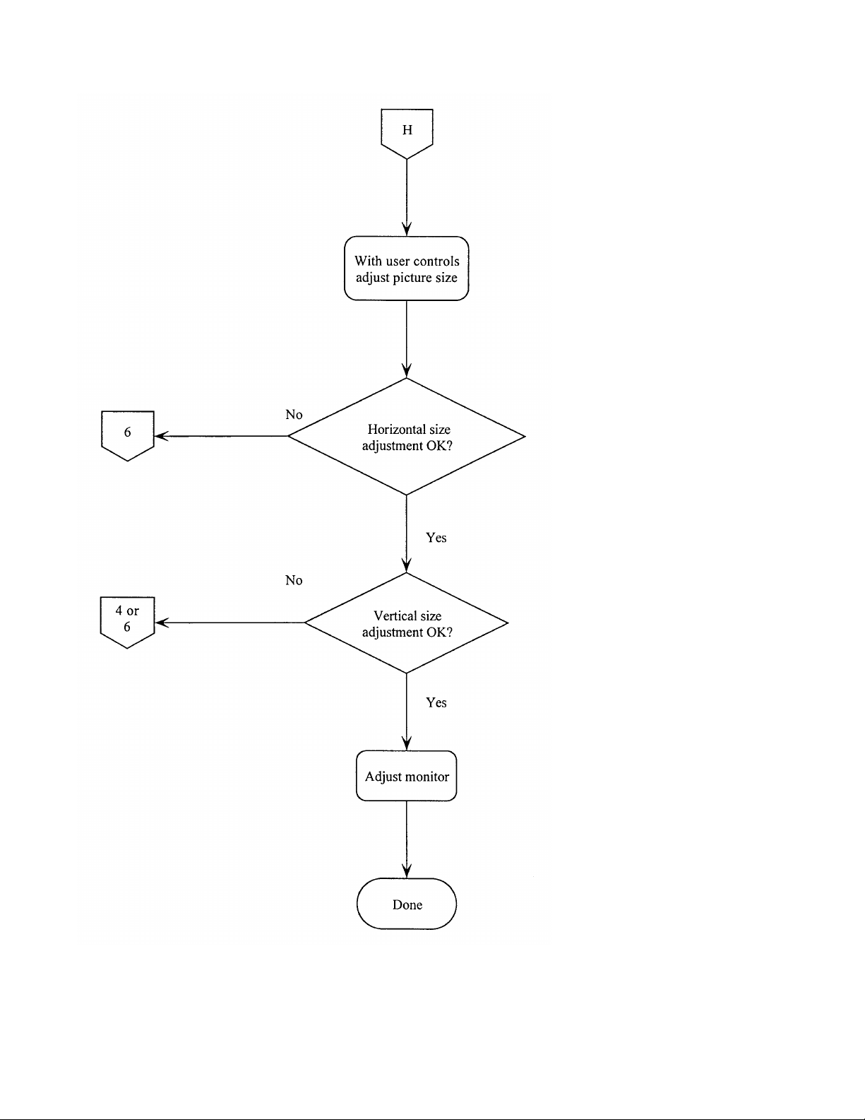
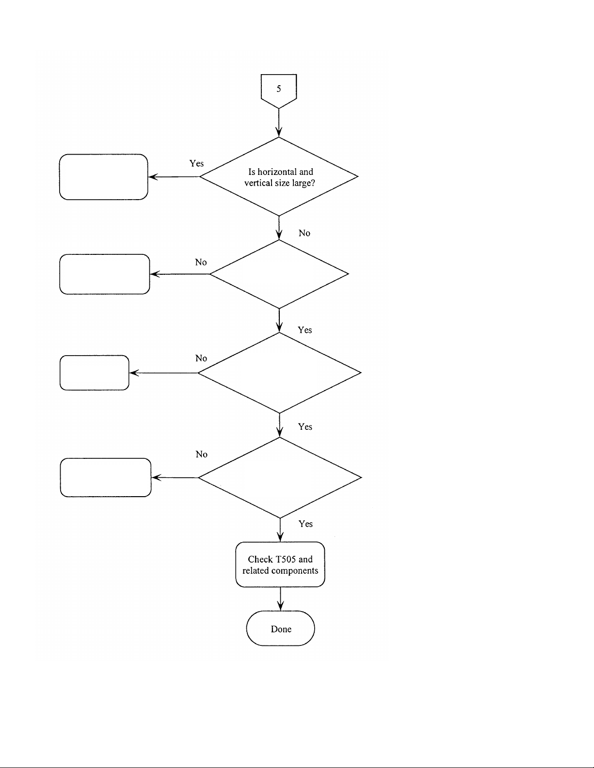
ABNORMAL IMAGE SIZE
(See Parts Level Board
Repair Section - page 15)
(See Parts Level Board
Repair Section - page 15)
- 12 -
Page 13
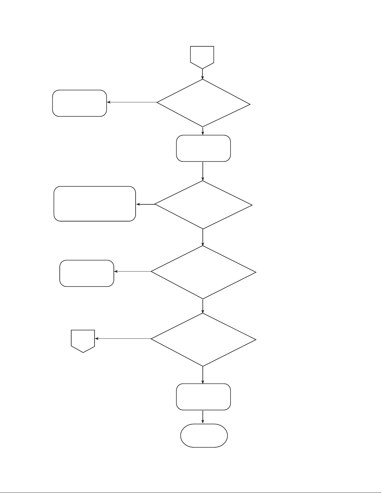
SHUT DOWN
I
Check power
supply
Check horizontal, vertical
deflection system and
check power supply
secondary voltages
Check high
voltage system
Yes
Yes
No
Is amber
LED blinking?
Yes
Check shutdown
log in IC901
Scan failure?
No
High voltage
failure?
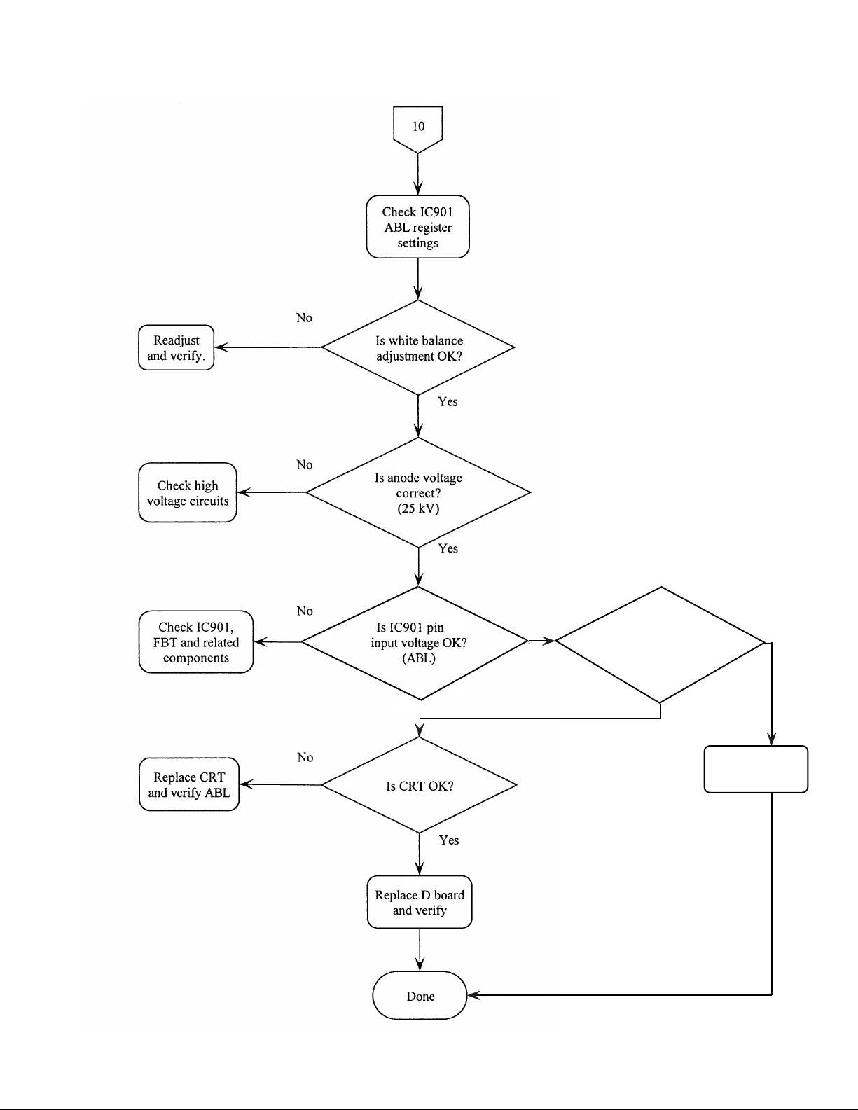
10
See Parts Level Board
Repair Section Page 15
No
No
ABL OK?
Yes
Set factory settings
inside IC901
Done
- 13 -
Page 14
NO COMMUNICATION
Is 5 volts present
at CN901 pin 2?
- 14 -
Page 15
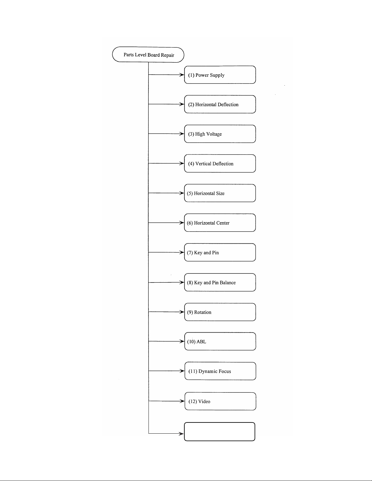
PARTS LEVEL BOARD REPAIR
(13) Convergence
- 15 -
Page 16
POWER SUPPLY
I
Check F601
and D601
Check Q503, Q507
and video board
Check IC603, IC604,
D622, R639, R621,
D614, D604
Replace Q602, Check
D608, D609, R605,
R614 and IC605
Replace parts,
verify voltages
Yes
Yes
No
Does power
supply make
chirping noise?
No
Tries to start?
No
No
Q602 OK?
Yes
Are D608, D609
R605, R614,
IC603 OK?
Check A board, if
OK, replace D board
Yes
Check secondary diodes, FPRD resistors,
IC501, IC901, IC902, IC605, IC401
and D902
No
Operating
Yes
Verify voltages and
adjust monitor
Done
- 16 -
Page 17

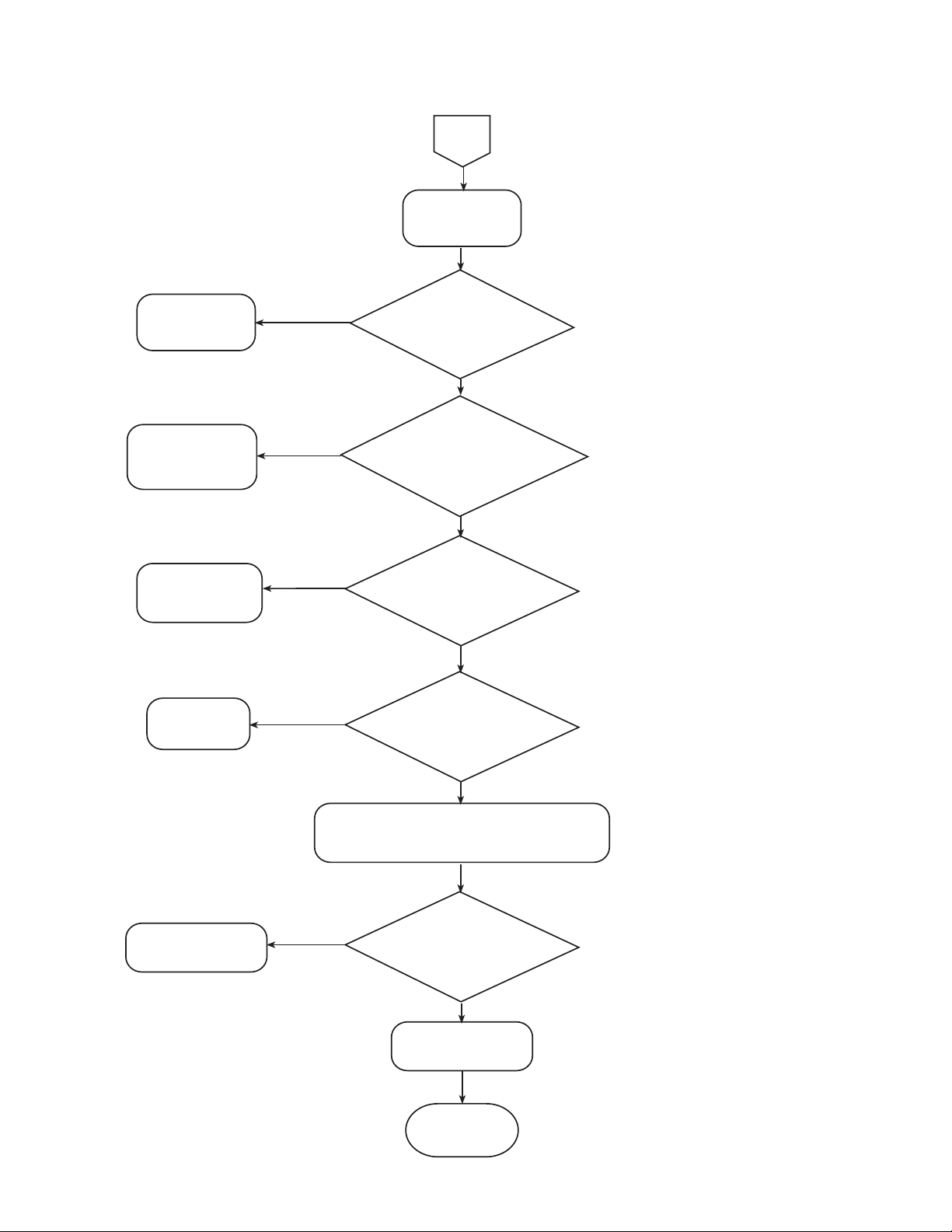
HORIZONTAL DEFLECTION
2
Check IC901 and
related components
Check IC902 and
related components
Check Q501,
Q502 & R504
Replace and check
related circuitry
No
No
No
No
Is IC901 pin 27
output OK?
(H-USYNC)
Yes
Is IC902 pin 17
output OK?
(H. Out)
Yes
Is Q501 emitter
output OK?
Yes
Is Q511 OK?
Replace and check
related circuitry
Replace and check
related circuitry
Yes
No
Is R623,
T504 and FPRDs
OK?
Yes
No
Is Q507 OK?
Yes
3
- 17 -
Page 18

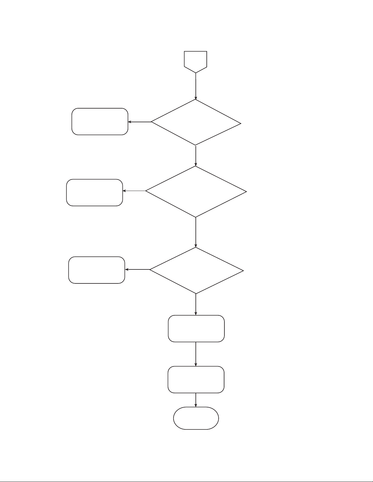
HIGH VOLT AGE
3
Replace Q503,
D509 and check
related components
Check Q510,
Q503 and related
components
Check IC501
and
related components
No
No
No
Is Q503 OK?
Yes
Is Q510, Q503 and
related
components OK?
Yes
Is IC501 pins 18 &
19 output
OK?
Change FBT and
verify operation
Yes
No
Is FBT OK?
Yes
Change DY, verify
operation and adjust
monitor
Done
- 18 -
Page 19
VERTICAL DEFLECTION
4
Check power
supply
Check IC902
& IC701
Verify IC401
and verify
No
No
No
Is +15V and
-15V OK?
Yes
Is
IC902 pin 8
(VSAW), IC701 pin 5
(VrefOut) & IC401
pin 4 waveforms
OK?
Yes
Is IC401 OK?
Change DY
Adjust
monitor
Done
- 19 -
Yes
Page 20
Check if IC501,
Q503 & Q510
OK
HORIZONTAL SIZE
Replace Q520 and
check related
components
Check IC902
Check IC501 and
related components
Is Q520 OK?
IC902 pin 9
(E/W) output
OK?
Is IC501 pins 15 & 19
output normal?
(Q503 Drive)
18
- 20 -
Page 21
Check IC901
No
HORIZONTAL CENTER
6
When
Power on is
pin 9 (DA8) of IC901
low (OV)?
Yes
Check D617, D618
& FBT
Replace corresponding
parts & adjust
monitor
No
No
No
Is
pin 4 (HCENT)
of IC901 working
OK?
Yes
Are
voltages at D617
and D618 OK?
Yes
Are
Q518 and Q506
and R529 OK?
Check
IC503
OK?
Yes
Check related
components or FRU
No
Replace
IC503
Yes
- 21 -
Done
Page 22
KEY AND PIN
7
Check IC902
related components
No
NoCheck IC501 and
IC902 pin 9 (E/W)
outputs normal?
Yes
Is IC501 and
related
components OK?
Yes
Check Q520 and
related components
Done
- 22 -
Page 23
KEY AND PIN BALANCE
8
Check IC901
No
Check if
IC902 pin 18
output OK?
Yes
Check related circuit
components, fix
and adjust monitor
Done
- 23 -
Page 24

Check for shorts,
check power supply
and check IC502
ROTATION
9
No
+15V and -15V
Normal?
Yes
Replace IC502 and
adjust monitor
No
IC502 OK?
Yes
Check rotation coil
and connections
Done
- 24 -
Page 25
Check B+ and
IC004 then readjust
and verify.
ABL FAILURE
(3)
Yes
Yes
Check
if R546,
R545 and FBT
related circuit
OK?
Yes
No
Replace parts
& verify
- 25 -
Page 26
IC902
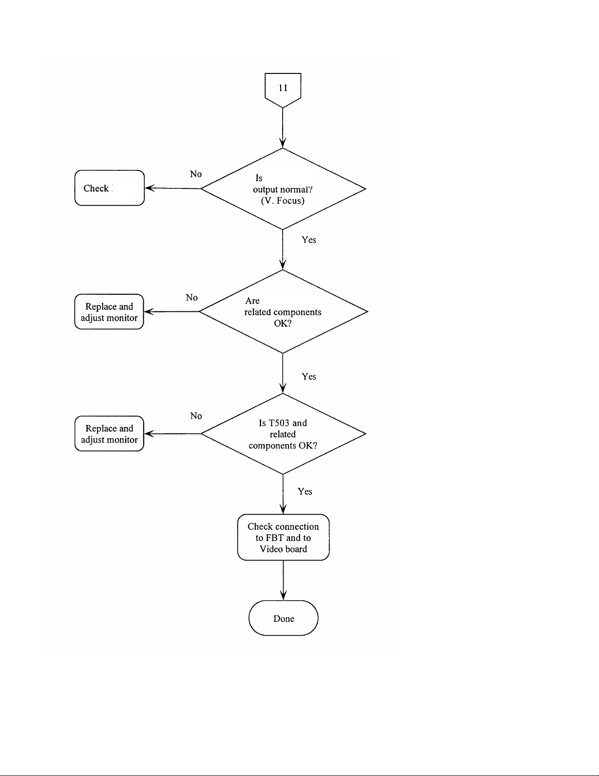
DYNAMIC FOCUS
IC902 pin 12
Q504, Q505 and
- 26 -
Page 27
VIDEO
12
Check connector
CN306,
IC901 & +5V
Check IC006
and
+5V
Check IC001
and
HV
Replace parts
& verify
No
No
No
No
Check if
2
I
C bus pins
1 & 2 of IC001
OK?
Check if
IC006 pins 17,
19 and 21 OK?
Yes
Check if
IC001 pins 18,
22 and 25 OK?
Yes
Check
if IC002
pins 1, 3 & 5
OK?
Check IC004
and +B
Check IC005,
G2 control circuit
and FBT
No
No
- 27 -
Yes
Are
cathode DC
levels correct?
Yes
Is
G2 voltage
correct?
Yes
Change CRT
Done
Page 28
CONVERGENCE
13
Check IC701,
IC605 outputs
pin 6 and
+15V power supply
Check IC702
+15V & -15V
line power
supply
Replace connector
and related
components
No
No
No
Check if
IC701 outputs
pins 8, 9, 6 and 7
are OK?
Yes
Check
if IC702
output pins 1, 6, 10,
and 15 are
OK?
Yes
Check
CN701 connector
if OK?
Yes
Yes
Replace
DY and verify
if OK?
No
Change CRT
Done
- 28 -
Page 29
NOTES:
- 29 -
Page 30
NOTES:
- 30 -
Page 31

- 31 -
Page 32

9-978-841-01
Sony Corporation
Sony T echnology Center
Product Quality Division
Service Promotion Department
- 32 -
English
98CJ74208-1
Printed in U.S.A.
© 1998.3
 Loading...