

Sony CXP85460, CXP85452 Datasheet
Description
The CXP85452/85460 are a highly integrated microcomputers composed of a 8-bit CPU, ROM, RAM,
and I/O ports. These chips feature many other highperformance circuits in a single-chip CMOS design,
including an A/D converter, serial interface,
timer/counter, time-base timer, on-screen display
function, I2C bus interface, PWM output, remote
control reception circuit, HSYNC counter, and
watchdog timer.
Futhermore, the CXP85452/85460 series provides
power-on reset and sleep functions which enable to
lower power consumption.
Features
• A wide instruction set (213 instructions) which covers various types of data
– 16-bit operation/multiplication and division/Boolean bit operation instructions
• Minimum instruction cycle 0.5µs at 8MHz
• Incorporated ROM capacity 52K bytes (CXP85452)
60K bytes (CXP85460)
• Incorporated RAM capacity 960 bytes
• Peripheral functions
– A/D converter 8-bit, 4-channel successive approximation method
(Conversion time of 20µs at 8MHz)
– Serial interface 8-bit clock sync type, 1 channel
– Timer 8-bit timer
8-bit timer/counter
19-bit time-base timer
– On screen display (OSD) function 12 × 18 dots, 384 character types, 15 character colors,
12lines of 32 characters,
black frame output/half blanking, shadow, background
color on full screen/half blanking,
double scanning, jitter elimination circuit
– I2C bus interface
– PWM output 14 bits, 1 channel
8 bits, 8 channels
– Remote control reception circuit 8-bit pulse measurement circuit, 6-state FIFO
– HSYNC counter 2 channels
– Watchdog timer
• Interruption 13 factors, 13 vectors, multi-interruption possible
• Standby mode SLEEP
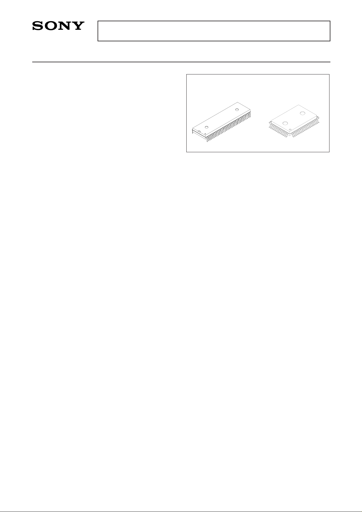
• Package 64-pin plastic SDIP/QFP
• Piggyback/evaluator CXP85400 64-pin ceramic PSDIP/PQFP
CXP85490 64-pin ceramic PSDIP (accommodates custom font)
Purchase of Sony's I2C components conveys a license under the Philips I2C Patent Rights to use these components
in an I2C system, provided that the system conforms to the I2C Standard Specifications as defined by Philips.
– 1 –
CXP85452/85460
E94323B86
CMOS 8-bit Single Chip Microcomputer
Sony reserves the right to change products and specifications without prior notice. This information does not convey any license by
any implication or otherwise under any patents or other right. Application circuits shown, if any, are typical examples illustrating the
operation of the devices. Sony cannot assume responsibility for any problems arising out of the use of these circuits.
64 pin SDIP (PIastic) 64 pin QFP (PIastic)
Structure
Silicon gate CMOS IC
– 2 –
CXP85452/85460
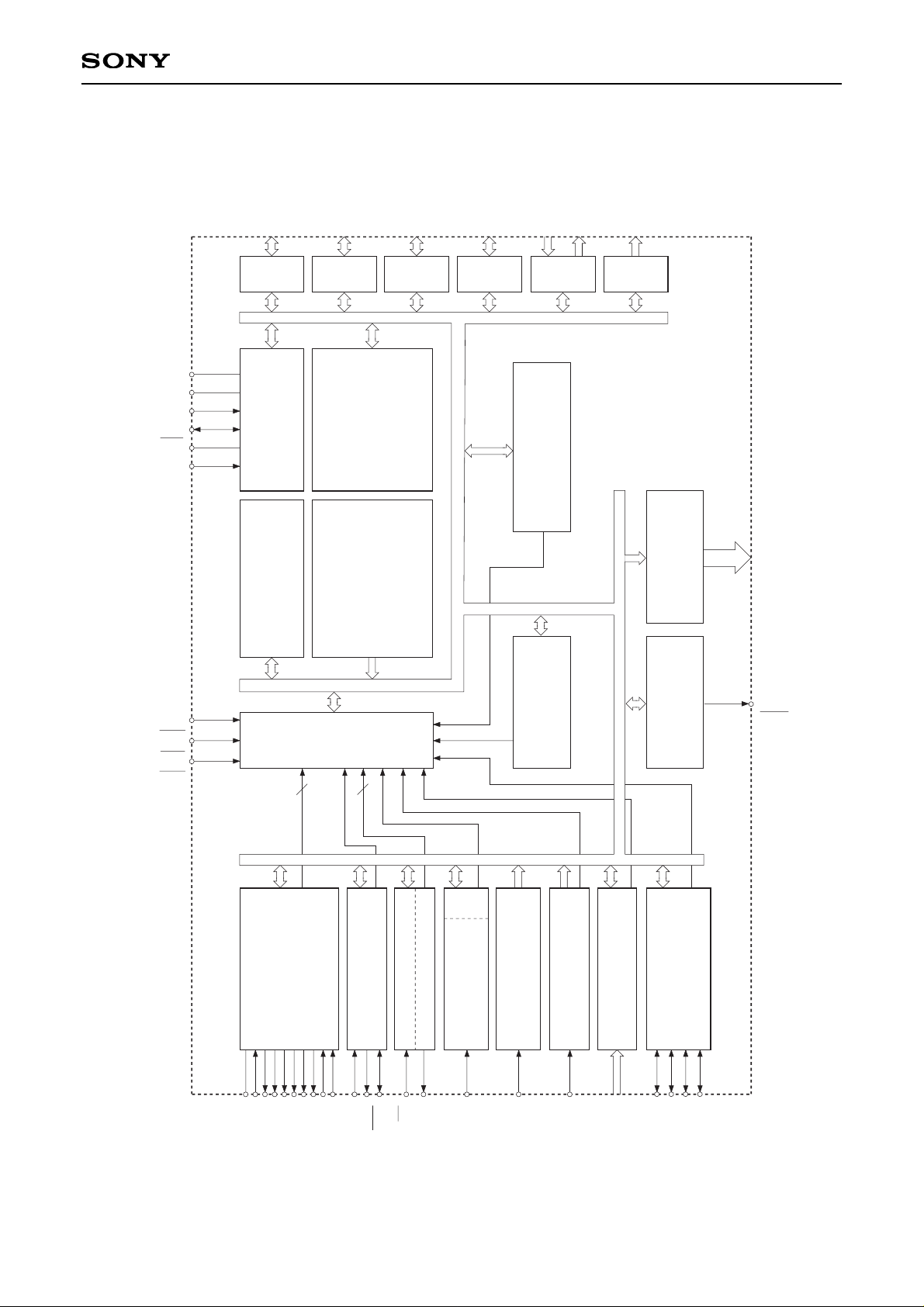
ON SCREEN DISPLAY
SERIAL INTERFACE UNIT
8 BIT TIMER/COUNTER 0
REMOCON FIFO
HSYNC COUNTER 0
HSYNC COUNTER 1
A/D CONVERTER
I
2
C BUS
INTERFACE UNIT
WATCH DOG TIMER
14 BIT PWM
8 BIT PWM
8CH
CLOCK GENERATOR/
SYSTEM CONTROL
RAM
960 BYTES
SPC700
CPU CORE
ROM
52K/60K
PRESCALER/
TIME BASE TIMER
PORT A
PORT B
PORT C
PORT D
PORT E
PORT F
2
2
V
SS
V
DD
MP
XTAL
EXTAL
RST
INT2
INT1
INT0
PWM0
to
PWM7
INTERRUPT
CONTROLLER
PWM
PA0 to PA7
PB0 to PB7
PC0 to PC7
PD0 to PD7
PE0 to PE5
PE6 to PE7
PF0 to PF7
XLC
EXLC
R
G
B
I
YS
YM
HSYNC
VSYNC
SI
SO
SCK
EC
TO
RMC
HS0
HS1
AN0
to
AN3
SCL0
SCL1
SDA0
SDA1
8 BIT TIMER 1
Block Diagram

– 3 –
CXP85452/85460
2
3
4
5
6
7
8
9
10
11
12
13
14
15
16
17
18
19
20
21
22
23
24
25
26
27
28
29
30
31
32
1
40
39
38
37
36
35
34
33
41
42
43
44
45
46
47
48
49
50
51
52
53
54
55
56
57
58
59
60
63
64
61
62
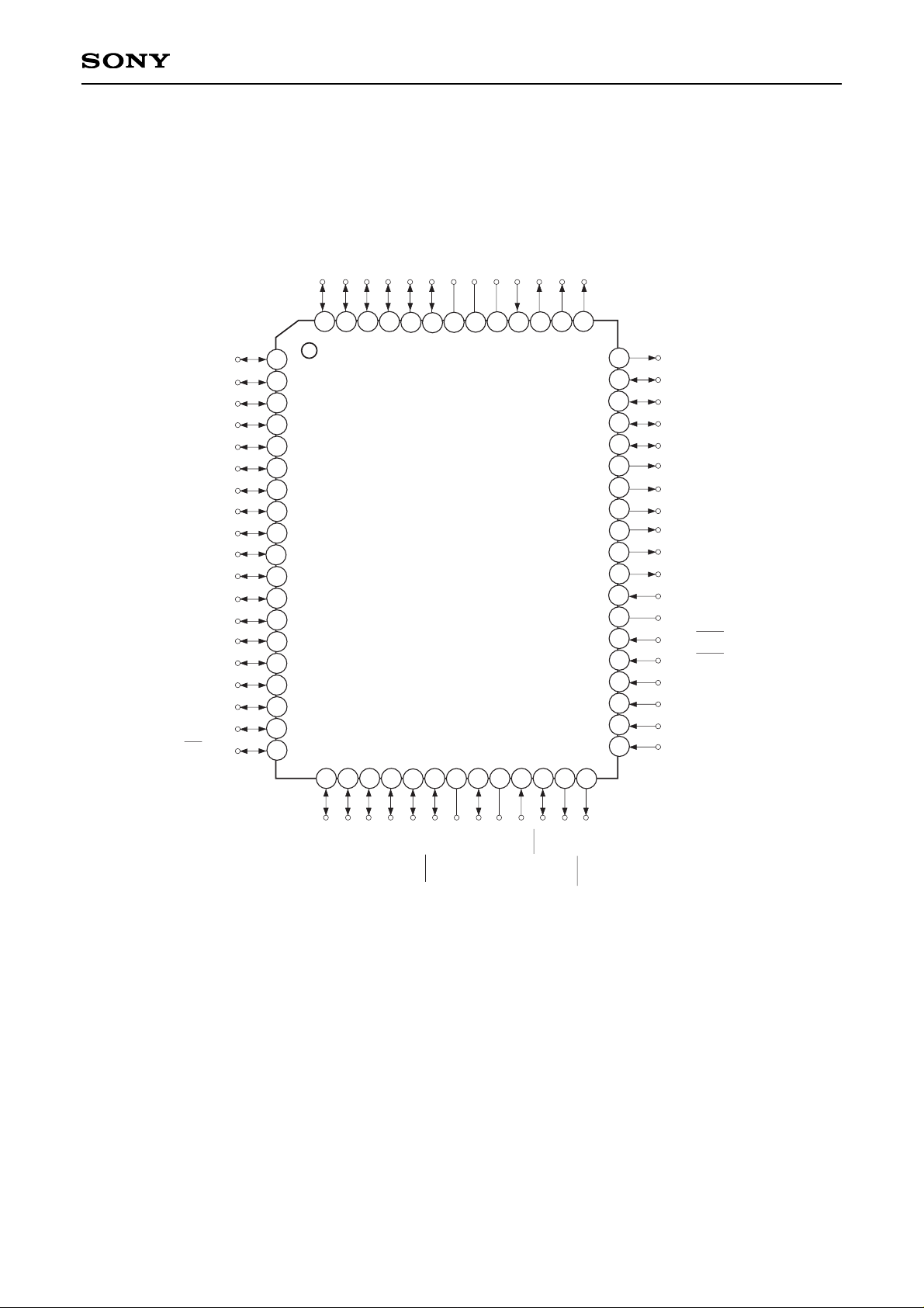
HSYNC/PA7
VSYNC/PA6
PA5
PA4
PA3
PA2
PA1
PA0
PB7
PB6
PB5
PB4
PB3
PB2
PB1
PB0
PC7
PC6
PC5
PC4
PC3
PC2
PC1
PC0
EC/PD7
RMC/PD6
HS1/PD5
HS0/PD4
SI/PD3
SO/PD2
SCK/PD1
V
SS
VDD
NC
V
SS
MP
PF0/PWM0
PF1/PWM1
PF2/PWM2
PF3/PWM3
PF4/PWM4/SCL0
PF5/PWM5/SCL1
PF6/PWM6/SDA0
PF7/PWM7/SDA1
YM
YS
I
B
G
R
EXLC
XLC
PE0/INT0
PE1/INT1
AN0/PE2
AN1/PE3
AN2/PE4
AN3/PE5
PE6/PWM
PE7/TO
RST
EXTAL
XTAL
PD0/INT2
Pin Assignment (Top View) 64-pin SDIP
Note) 1. NC (Pin 63) is always connected to VDD.
2. Vss (Pins 32 and 62) are both connected to GND.
3. MP (Pin 61) is always connected to GND.
– 4 –
CXP85452/85460
Note) 1. NC (Pin 56) is always connected to VDD.
2. Vss (Pins 26 and 58) are both connected to GND.
3. MP (Pin 55) is always connected to GND.
Pin Assignment (Top View) 64-pin QFP
PA1
PA0
PB7
PB6
PB5
PB4
PB3
PB2
PB1
PB0
PC7
PC6
PC5
PC4
PC3
PC2
PC1
PC0
EC/PD7
2
3
4
5
6
7
8
9
10
11
12
13
14
15
16
17
18
19
1
PF3/PWM3
PF4/PWM4/SCL0
PF5/PWM5/SCL1
PF6/PWM6/SDA0
PF7/PWM7/SDA1
YM
YS
I
B
G
R
EXLC
XLC
PE0/INT0
PE1/INT1
AN0/PE2
AN1/PE3
AN2/PE4
AN3/PE5
40
39
38
37
36
35
34
33
41
42
43
44
45
46
47
48
49
50
51
PA2
PA3
PA4
PA5
PA6/VSYNC
PA7/HSYNC
V
SS
V
DD
NC
MP
PF0/PWM0
PF1/PWM1
PF2/PWM2
52
53
54
55
56
57
58
59
60
63
64
61
62
RMC/PD6
HS1/PD5
HS0/PD4
SI/PD3
SO/PD2
SCK/PD1
V
SS
INT2/PD0
XTAL
EXTAL
RST
TO/PE7
PWM/PE6
20
21
22
23
24
25
26
27
28
29
30
31
32
(Port A)
8-bit I/O port. I/O can be set in a unit of single bits.
(8 pins)
(Port B)
8-bit I/O port. I/O can be set in a unit of single bits.
(8 pins)
(Port C)
8-bit I/O port. I/O can be set in a unit of single bits.
(8 pins)
(Port D)
8-bit I/O port. I/O
can be set in a unit
of single bits.
12mA sink current
drive possible.
(8 pins)
(Port E)
8-bit port. Lower
6 bits are for inputs;
upper 2 bits are for
outputs.
(8 pins)
(Port F)
8-bit output port.
Large current
(12mA) N-ch open
drain output.
Lower 4 bits are
mid-voltage drive
(12V); upper 4 bits
are 5V drive.
(8 pins)
OSD display 6-bit output pin. (6 pins)
– 5 –
CXP85452/85460
Pin Description
Symbol
PA0 to PA5
PA6/VSYNC
PA7/HSYNC
PB0 to PB7
PC0 to PC7
PD0/INT2
PD1/SCK
PD2/SO
PD3/SI
PD4/HS0
PD5/HS1
PD6/RMC
PD7/EC
PE0/INT0
PE1/INT1
PE2/AN0
to
PE5/AN3
PE6/PWM
PE7/TO
PF0/PWM0
to
PF3/PWM3
PF4/PWM4/
SCL0
PF5/PWM5/
SCL1
PF6/PWM6/
SDA0
PF7/PWM7/
SDA1
R, G, B, I, YS, YM
I/O
I/O/Input
I/O/Input
I/O
I/O
I/O/Input
I/O/I/O
I/O/Output
I/O/Input
I/O/Input
I/O/Input
I/O/Input
I/O/Input
Input/Input
Input/Input
Output/Output
Output/Output
Output/Output
Output/Output/
I/O
Output/Output/
I/O
Output
I/O Description
OSD display vertical synchronization signal input pin.
OSD display horizontal synchronization signal input pin.
Input pin for external interruption request.
Active when falling edge.
Serial clock I/O pin.
Serial data output pin.
Serial data input pin.
HSYNC counter (CH0) input pin.
HSYNC counter (CH1) input pin.
Remote control reception circuit input pin.
External event input pin for timer/counter.
Input pin for external interruption request.
Active when falling edge.
(2 pins)
Analog input pin for A/D converter.
(4 pins)
14-bit PWM output pin.
(CMOS output)
Timer/counter rectangular wave output pin.
8-bit PWM output pin.
(8 pins)
I2C bus interface transfer clock I/O pin.
(2 pins)
I2C bus interface transfer data I/O pin.
(2 pins)

– 6 –
CXP85452/85460
Symbol
EXLC
XLC
EXTAL
XTAL
RST
MP
NC
VDD
Vss
Input
Output
Input
Output
I/O
Input
OSD display clock oscillation I/O pin.
Oscillation frequency is determined by the external L and C.
Crystal connection pin for system clock oscillation. When using an external
clock, input to EXTAL pin and leave XTAL pin open.
System reset pin for active at low level. This pin becomes I/O pin, and
outputs low level at the power on with power-on reset function executed.
(Mask option)
Test mode input pin. Always connect to GND.
NC. Under normal operation, connect to VDD.
Positive supply voltage pin.
GND. Both Vss pins should be connected to common GND.
I/O Description
– 7 –
CXP85452/85460
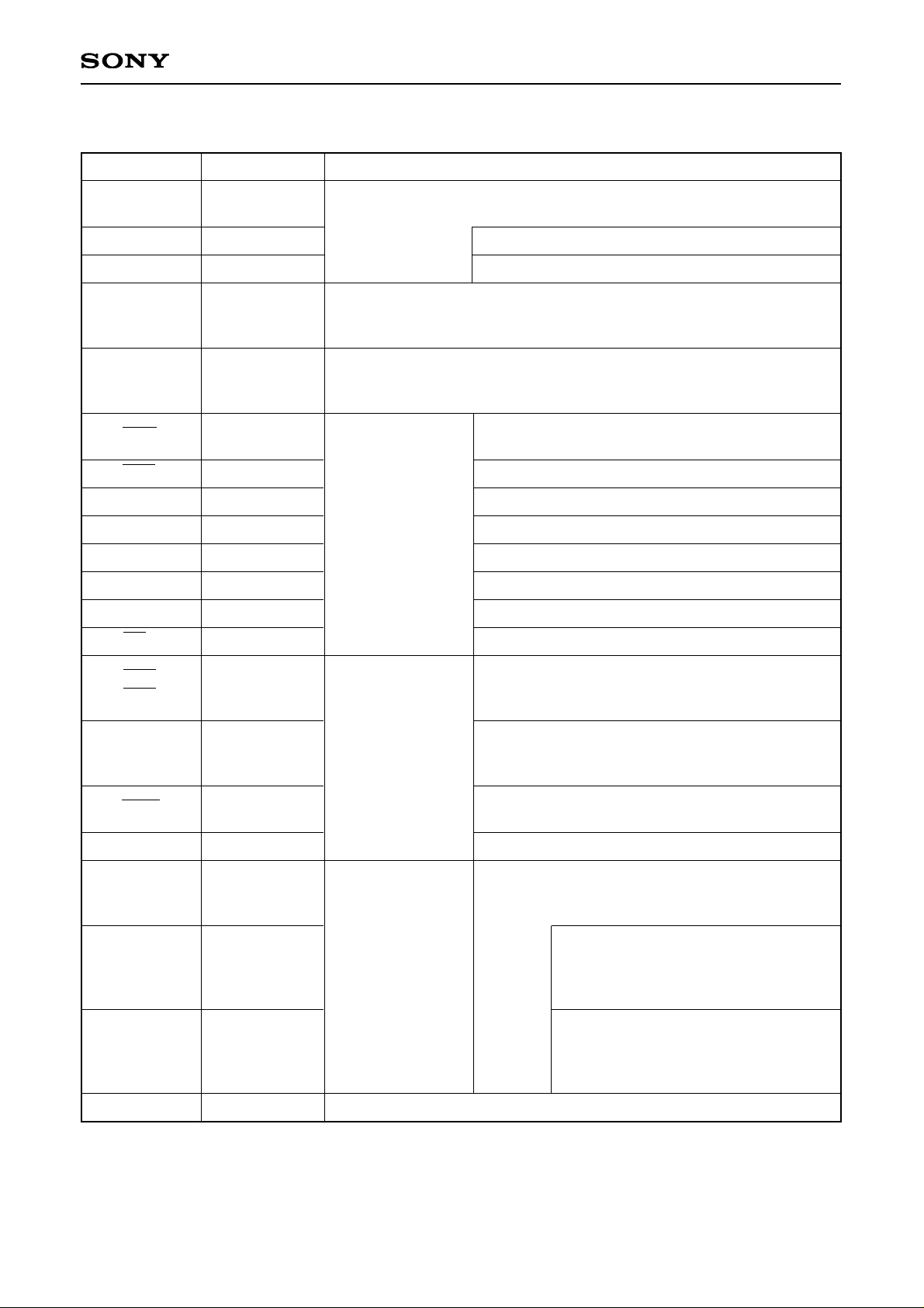
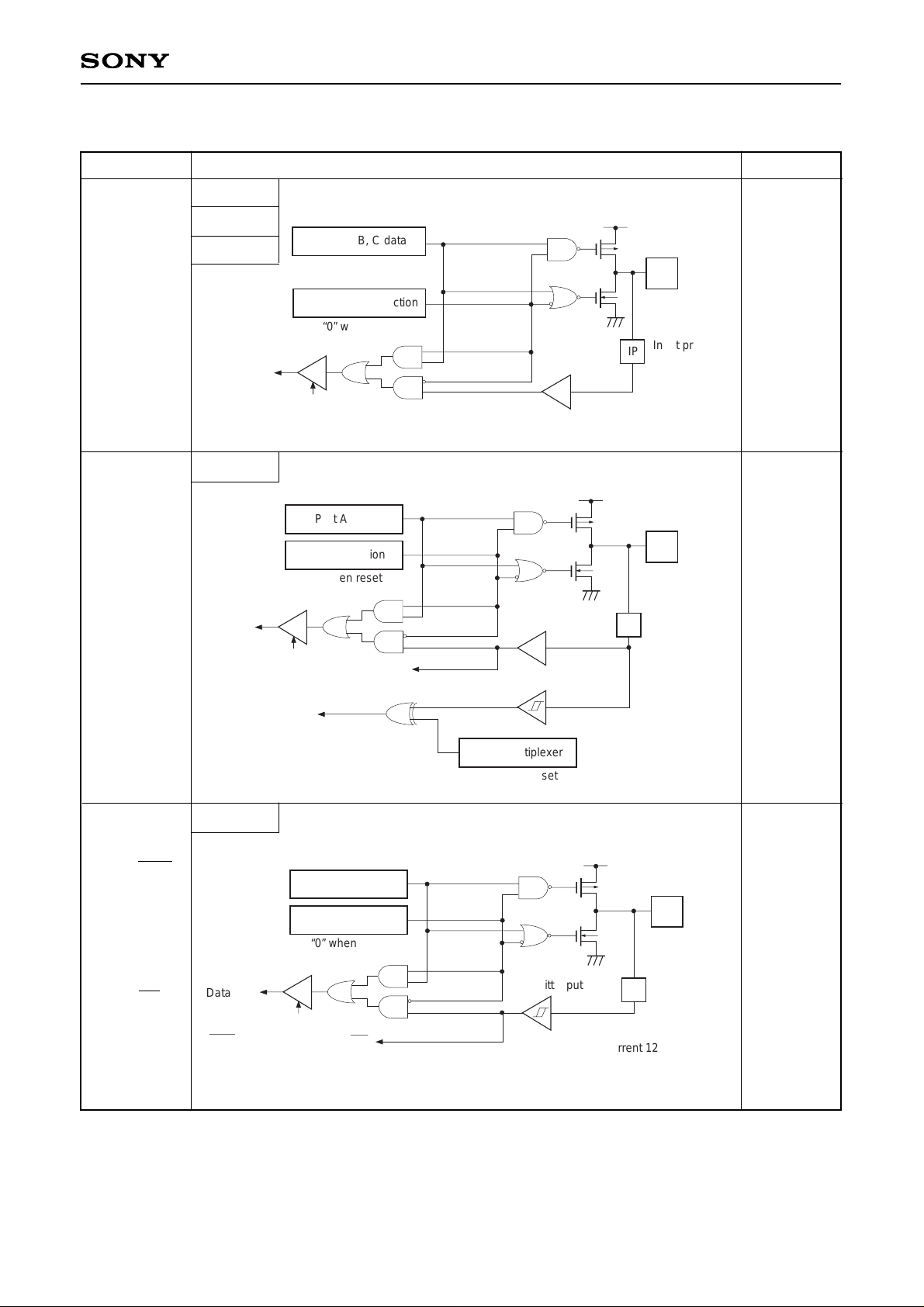
Input/Output Circuit Formats for Pins
Port A
Port B
Port C
Port A
Port D
22 pins
2 pins
6 pins
Hi-Z
Hi-Z
Hi-Z
Pin When resetCircuit format
PA0 to PA5
PB0 to PB7
PC0 to PC7
PA6/VSYNC
PA7/HSYNC
PD0/INT2
PD3/SI
PD4/HS0
PD5/HS1
PD6/RMC
PD7/EC
Ports A, B, C data
Ports A, B, C direction
“0” when reset
Data bus
RD
(Ports A, B, C)
Port A data
Input protection
IP
circuit
Data bus
Data bus
Port A direction
RD (Port A)
VSYNC
HSYNC
“0” when reset
Port D data
Port D direction
“0” when reset
Schmitt input
Input multiplexer
“0” when reset
Schmitt input
IP
∗
IP
RD (Port D)
INT2, SI, HS0, HS1, RMC, EC
∗
Large current 12mA
 Loading...