

Sony CXP84548, CXP84540 Datasheet
CMOS 8-bit Single Chip Microcomputer
Description
The CXP84540/84548 is a CMOS 8-bit microcomputer integrating on a single chip an A/D converter,
serial interface, timer/counter, time-base timer, capture
timer/counter, PWM output and the like besides the
basic configurations of 8-bit CPU, ROM, RAM and I/O
port.
The CXP84540/84548 also provide a sleep/stop
functions that enable to execute the power-on reset
function or lower the power consumption.
Features
• Wide range instruction system (213 instructions)
which covers various of data
— 16-bit arithmetic/multiplication and
division/Boolean bit operation instructions
• Minimum instruction cycle 143ns at 28MHz operation (4.5 to 5.5V)
200ns at 20kHz operation (3.0 to 5.5V)
• Incorporated ROM capacity 40K bytes (CXP84540)
48K bytes (CXP84548)
• Incorporated RAM capacity 1472 bytes
• Peripheral functions
— A/D converter 8 bits, 8 channels, successive approximation method
(Conversion time of 1.93µs / at 28MHz, 2.7µs / at 20MHz)
— Serial interface Incorporated 8-bit, 8-stage FIFO (Auto transfer for 1 to 8 bytes,
latch output function, MSB/LSB first selectable), 1 channel
8-bit clock syncronization, 1 channel
— Timer 8-bit timer
8-bit timer/counter
19-bit time-base timer
16-bit capture time/counter
— PWM output 8 bits, 2 channels
• Interruption 14 factors, 14 vectors, multi-interruption possible
• Standby mode Sleep/Stop
• Package 80-pin plastic QFP/LQFP
80-pin plastic LFLGA
• Piggyback/evaluator CXP84500
Structure
Silicon gate CMOS IC
– 1 –
E96528B9X-PS
Sony reserves the right to change products and specifications without prior notice. This information does not convey any license by
any implication or otherwise under any patents or other right. Application circuits shown, if any, are typical examples illustrating the
operation of the devices. Sony cannot assume responsibility for any problems arising out of the use of these circuits.
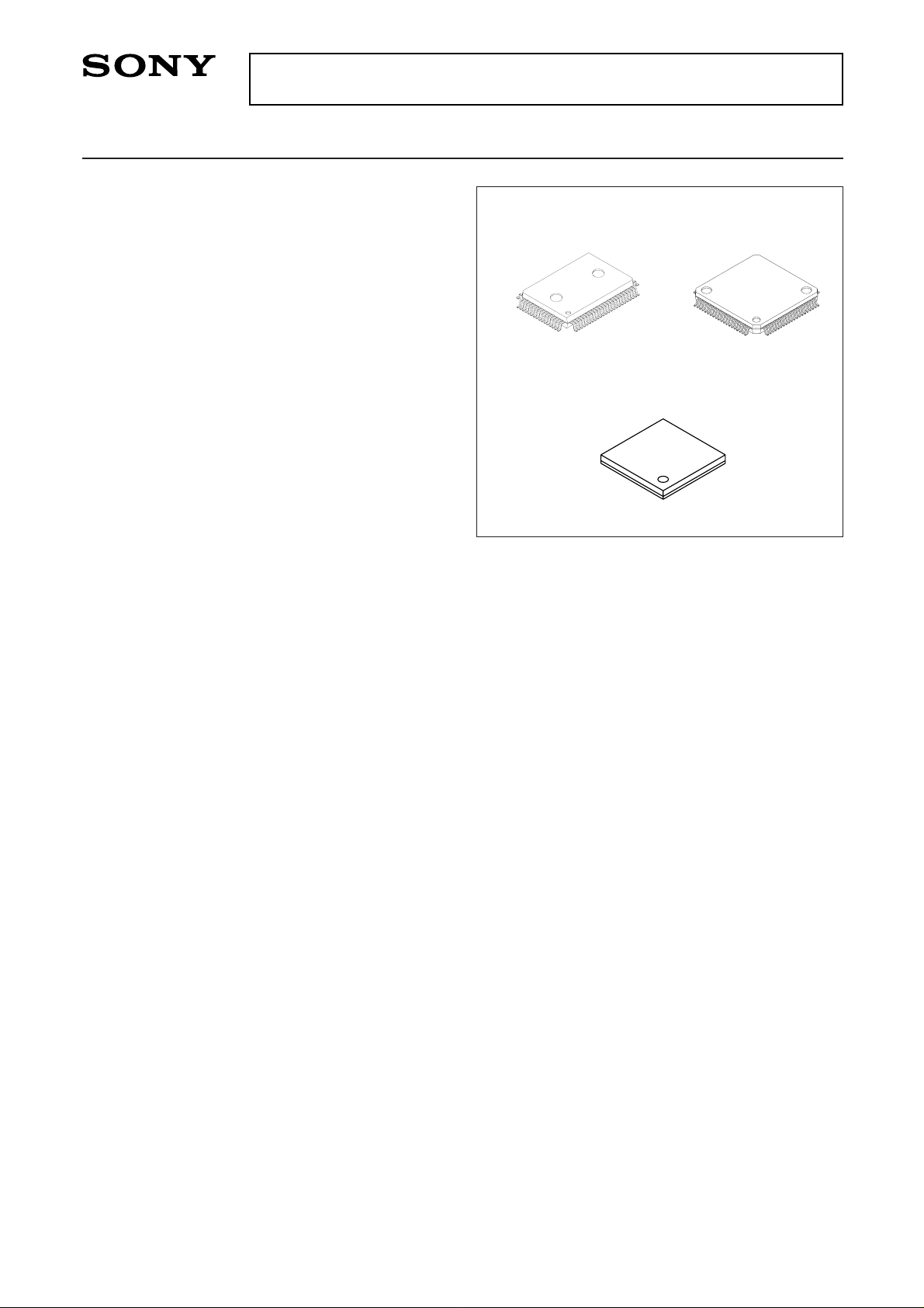
CXP84540/84548
80 pin LQFP (Plastic)
80 pin LFLGA (Plastic)
80 pin QFP (Plastic)

– 2 –
CXP84540/84548
8
AN0 to AN7
PWM0
PWM1
CS0
SI0
SO0
SCK0
SI1
SO1
SCK1
TO
CINT
EC1
EC0
A/D CONVERTER
AVss
AV
REF
8-BIT PWM GENERATOR 0
SERIAL
INTERFACE
UNIT (CH0)
FIFO
SERIAL INTERFACE UNIT (CH1)
8-BIT TIMER/COUNTER 0
8-BIT TIMER 1
16-BIT CAPTURE
TIMER/COUNTER 2
INTERRUPT CONTROLLER
INT0
INT1
INT2
INT3
NMI
SPC700
CPU CORE
ROM
40K/48K BYTES
CLOCK
GENERATOR/
SYSTEM CONTROL
RAM
1472 BYTES
PRESCALER/
TIME BASE TIMER
EXTAL
XTAL
V
DD
Vss
PORT A
8
8
8
4
4
8
PA0 to PA7
PB0 to PB7
PC0 to PC7
PD0 to PD7
PE0 to PE3
PE4 to PE7
PF0 to PF7
PG0 to PG7
PI0 to PI7
RST
8
8
8
PORT B
PORT C
PORT D
PORT E
PORT F
PORT G
PORT I
PH0 to PH7
8
PORT H
2
2
LAT0
8-BIT PWM GENERATOR 1
Block Diagram
– 3 –
CXP84540/84548
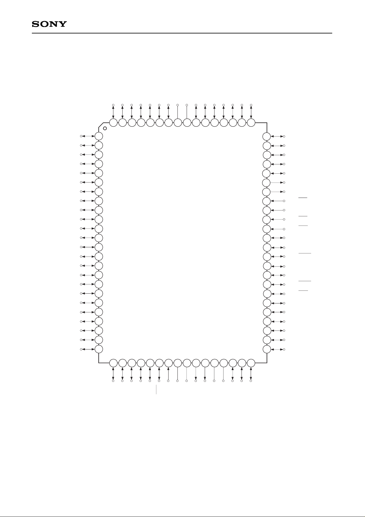
Pin Assignment (Top View) 80-pin QFP package
2
3
4
5
6
7
8
9
10
11
12
13
14
15
16
17
18
19
20
21
22
23
24
25
26
27 28
29
30
40
39
38
37
36
35
34
31
32
33
41
42
43
44
45
46
47
48
49
50
51
52
53
54
55
56
57
58
59
60
70
69
68
67
63
64
65
66
61
62
71
72
73
74
75
76
77
78
79
80
1
PE1/EC1
PI4
PI3/INT3
PI2/INT2
PI1/INT1
PI0/INT0
PE5/TO/PWM1
PE4/PWM0
PE3/NMI
PE2/CINT
PE0/EC0
PB7/SO1
PB6/SI1
PB5/SCK1
PB4/SO0
PB3/SI0
PB2/SCK0
PB1/CS0
PB0/LAT0
PA7/AN7
PA6/AN6
PA5/AN5
PA4/AN4
PA3/AN3
PH3
PH4
PH5
PH6
PH7
RST
EXTAL
XTAL
V
SS
PE6
PE7
AV
SS
AV
REF
PA0/AN0
PA1/AN1
PA2/AN2
PF3
PF4
PF5
PF6
PF7
PD0
PD1
PD2
PD3
PD4
PD5
PD6
PD7
PC0
PC1
PC2
PC3
PC4
PC5
PC6
PC7
PH0
PH1
PH2
PF2
PF1
PF0
PG7
PG6
PG5
PG4
NC
V
DD
PG3
PG2
PG1
PG0
PI7
PI6
PI5
Note) NC (Pin 73) is left open. However, this pin is used for the Flash EEPROM
incorporated version (CXP845F60).
– 4 –
CXP84540/84548
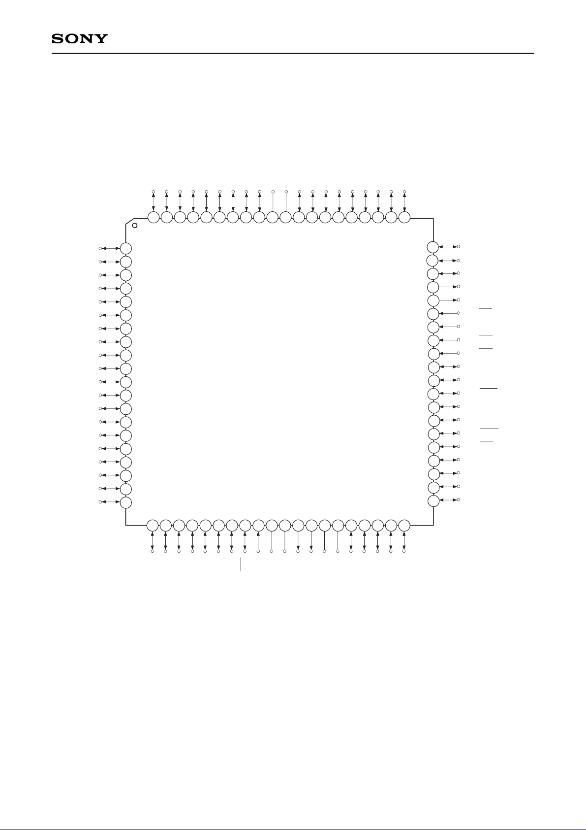
Pin Assignment (Top View) 80-pin LQFP package
Note) NC (Pin 73) is left open.
PF5
PF6
PF7
PD0
PD1
PD2
PD3
PD4
PD5
PD6
PD7
PC0
PC1
PC2
PC3
PC4
PC5
PC6
PC7
PH0
PI2/INT2
PI1/INT1
PI0/INT0
PE5/TO/PWM1
PE4/PWM0
PE3/NMI
PE2/CINT
PE1/EC1
PE0/EC0
PB7/SO1
PB6/SI1
PB5/SCK1
PB4/SO0
PB3/SI0
PB2/SCK0
PB1/CS0
PB0/LAT0
PA7/AN7
PA6/AN6
PA5/AN5
PH1
PH2
PH3
PH4
PH5
PH6
PH7
RST
EXTAL
XTAL
V
SS
PE6
PE7
AV
SS
AV
REF
PA0/AN0
PA1/AN1
PA2/AN2
PA3/AN3
PA4/AN4
PF4
PF3
PF2
PF1
PF0
PG7
PG6
PG5
PG4
NC
V
DD
PG3
PG2
PG1
PG0
PI7
PI6
PI5
PI4
PI3/INT3
2
3
4
5
6
7
8
9
10
11
12
13
14
15
16
17
18
19
20
21
22
23
24
25
26
27
28
29
30
40
39
38
37
36
35
34
31
32
33
70
69
68
67
65
66
71
72
73
74
75
76
77
78
79
80
1
41
42
43
44
45
46
47
48
49
50
51
52
53
54
55
56
57
58
59
60
63
64
61
62
– 5 –
CXP84540/84548
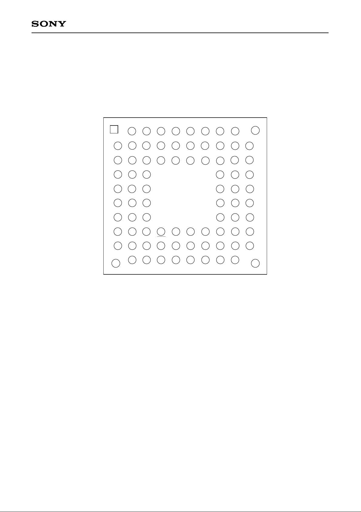
Pin Assignment (Top View) 80-pin LFLGA package
Note) NC (Pin 71) is left open.
80
78
75
72
69
67
65
62
2
1
79
76
73
70
66
63
61
60
5
3
4
77
74
71
68
64
59
58
7
6
8
57
56
55
9
10
11
54
53
52
12
13
14
51
50
49
15
16
17
48
46
47
18
19
24
28
31
34
37
44
43
45
20
21
23
26
30
33
36
39
41
42
22
25
27
29
32
35
38
40
PF4 PF2 PG7 PG4 PG3 PG1 PI7 PI4
PF5PF6 PF3 PF0 PG5 V
DD PG0 PI5 PI3 PI2
PF7PD1 PD0 PF1 PG6 NC PG2 PI6 PI1 PI0
PD2PD3 PD4 PE5 PE4 PE3
PD6PD5 PD7 PE2 PE1 PE0
PC1PC0 PC2 PB7 PB6 PB5
PC4PC3 PC5 PB4 PB2 PB3
PC7PC6 PH4 RST V
SS AVSS PA1 PB0 PA7 PB1
PH1PH0 PH3 PH6 XTAL PE7 PA0 PA3 PA5 PA6
PH2 PH5 PH7 EXTAL PE6 AVREF PA2 PA4
– 6 –
CXP84540/84548
Pin Description
Symbol I/O Description
I/O/Analog input
PA0/AN0
to
PA7/AN7
(Port A)
8-bit I/O port. I/O can be
set in a unit of single bits.
Incorporation of the
pull-up resistance can be
set through the software in
a unit of 4 bits.
(8 pins)
Analog inputs to A/D converter.
(8 pins)
I/OPC0 to PC7
(Port C)
8-bit I/O port. I/O can be set in a unit of single bits. Can drive 12mA sync
current. Incorporation of pull-up resistor can be set through the software
in a unit of 4 bits.
(8 pins)
I/OPD0 to PD7
(Port D)
8-bit I/O port. I/O can be set in a unit of single bits. Incorporation of pullup resistor can be set through the software in a unit of 4 bits.
(8 pins)
I/OPF0 to PF7
(Port F)
8-bit I/O port. I/O can be set in a unit of single bits. Incorporation of
pull-up resistor can be set through the software in a unit of 4 bits.
(8 pins)
Input/Input
Input/Input
Input/Input
Input/Input
Output/Output
Output/Output/
Output
Output
Output
PE0/EC0
PE1/EC1
PE2/CINT
PE3/NMI
PE4/PWM0
PE5/TO/
PWM1
PE6
PE7
(Port E)
8-bit port. Lower 4 bits
are for inputs; upper
4 bits are for outputs.
(8 pins)
External event inputs for timer/counter.
(2 pins)
Capture trigger input.
Non-maskable interruption request input.
8-bit PWM0 output.
Rectangular wave output for 16-bit timer/
counter and 8-bit PWM1 output.
I/O/Output
I/O/Input
I/O/I/O
I/O/Input
I/O/Output
I/O/I/O
I/O/Input
I/O/Output
PB0/LAT0
PB1/CS0
PB2/SCK0
PB3/SI0
PB4/SO0
PB5/SCK1
PB6/SI1
PB7/SO1
(Port B)
8-bit I/O port. I/O can be
set in a unit of single bits.
Incorporation of pull-up
resistor can be set
through the software in a
unit of 4 bits.
(8 pins)
Latch output for serial interface (CH0).
Chip select input for serial interface (CH0).
Serial clock I/O (CH0).
Serial data input (CH0).
Serial data output (CH0).
Serial clock I/O (CH1).
Serial data input (CH1).
Serial data output (CH1).
– 7 –
CXP84540/84548
Symbol I/O Description
I/OPG0 to PG7
(Port G)
8-bit I/O port. I/O can be set in a unit of single bits. Incorporation of pullup resistor can be set through the software in a unit of 4 bits.
(8 pins)
I/OPH0 to PH7
(Port H)
8-bit I/O port. I/O and standby release input function can be set in a unit
of single bits. Incorporation of pull-up resistor can be set through the
software in a unit of 4 bits.
(8 pins)
I/O/Input
PI0/INT0
to
PI3/INT3
I/O
PI4 to PI7
Input
Crystal connectors for system clock oscillation. When the clock is supplied
externally, input it to EXTAL; opposite phase clock should be input to XTAL.
EXTAL
OutputXTAL
I/O
System reset for active at Low level. This pin is I/O pin, and outputs Low
level at the power on with the power-on reset function executed. (Mask
option)
RST
No connected. Leave this pin open.
However, this is used for the Flash EEPROM incorporated version
(CXP845F60).
NC
Input
Reference voltage input for A/D converter.
AVREF
A/D converter GND.
AVss
Positive power supply.
VDD
GND
Vss
(Port I)
8-bit I/O port. I/O can be set in a unit of single
bits. Incorporation of pull-up resistor can be set
through the software in a unit of 4 bits.
(8 pins)
External interruption
request inputs.
(4 pins)
– 8 –
CXP84540/84548
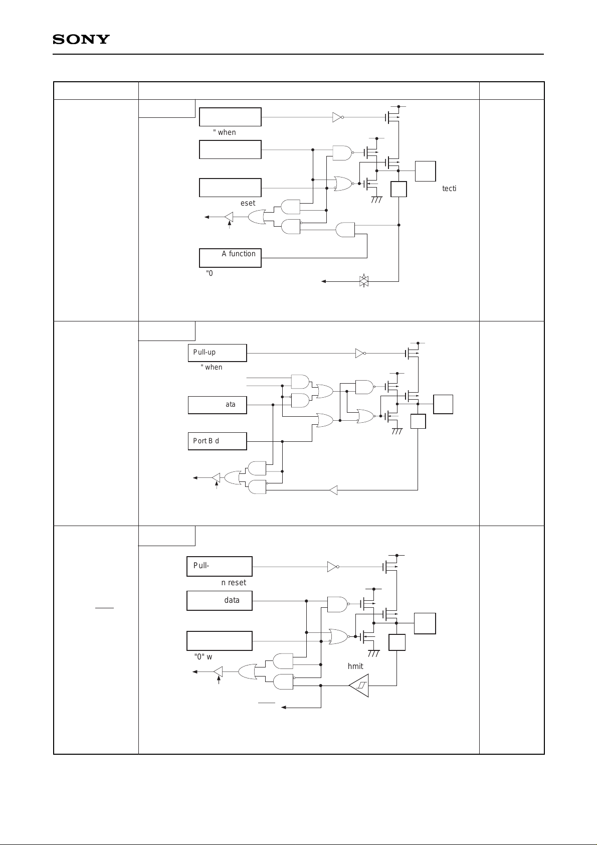
Data bus
RD (Port B)
Port B direction
IP
Port B data
Pull-up resistor
"0" when reset
"0" when reset
LAT0
Latch output enable
∗
Pull-up transistor
approx. 100kΩ (VDD = 4.5 to 5.5V)
approx. 300kΩ (VDD = 3.0 to 3.6V)
∗
Data bus
RD (Port B)
Port B direction
IP
Port B data
Pull-up resistor
"0" when reset
"0" when reset
Schmitt input
CS0
SI0
SI1
∗
Pull-up transistor
approx. 100kΩ (VDD = 4.5 to 5.5V)
approx. 300kΩ (VDD = 3.0 to 3.6V)
∗
Port B
8 pins
Hi-Z
Hi-Z
When reset
PA0/AN0
to
PA7/AN7
PB0/LAT0
Port B
1 pin
3 pins
Hi-Z
PB1/CS0
PB3/SI0
PB6/SI1
Data bus
RD (Port A)
Port A direction
IP
Port A data
Pull-up resistor
Port A function
selection
Input protection
circuit
"0" when reset
"0" when reset
"0" when reset
Input multiplexer
A/D converter
∗
Pull-up transistor
approx. 100kΩ (VDD = 4.5 to 5.5V)
approx. 300kΩ (VDD = 3.0 to 3.6V)
∗
Input/Output Circuit Formats for Pins
Port A
Pin
Circuit format
– 9 –
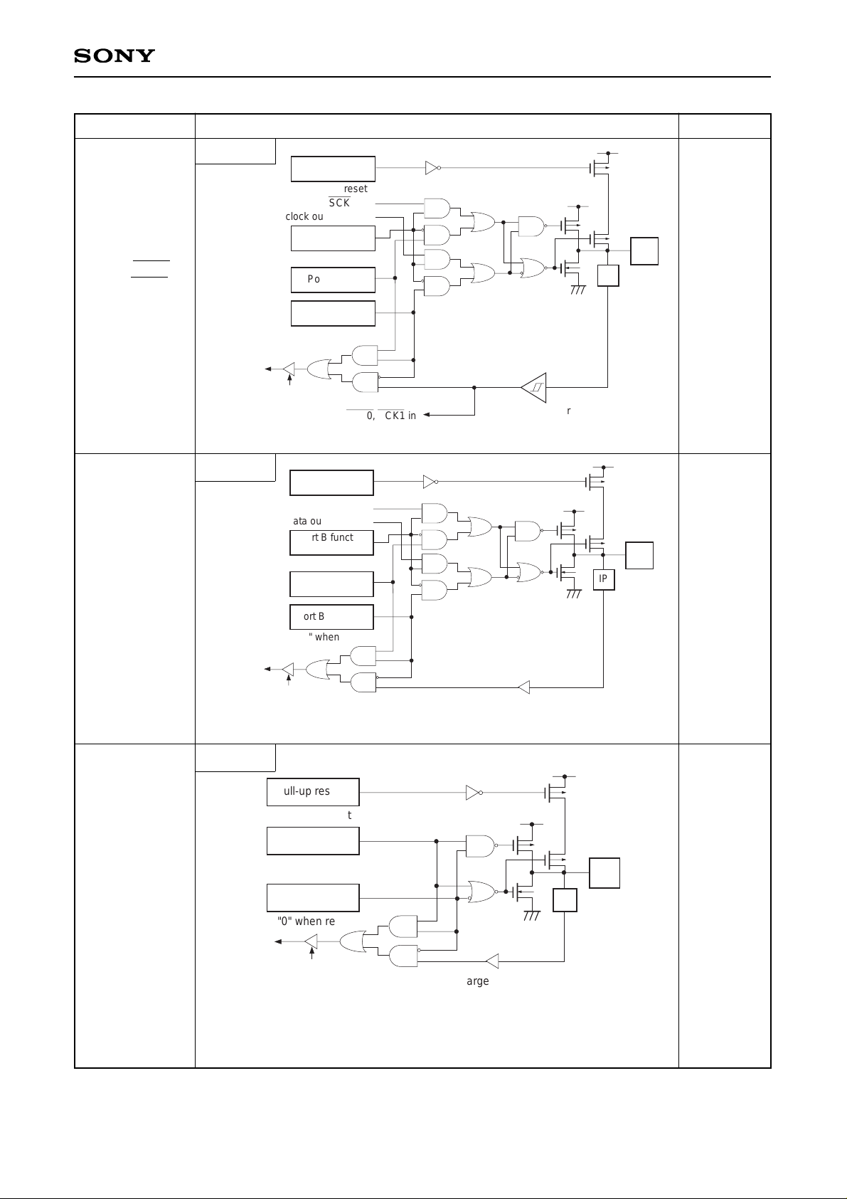
CXP84540/84548
Port B
2 pins
Hi-Z
Hi-Z
PB2/SCK0
PB5/SCK1
PB4/SO0
PB7/SO1
Port C
2 pins
8 pins
Hi-Z
PC0 to PC7
Data bus
RD (Port B)
IP
Port B function
selection
"0" when reset
Schmitt input
SCK0, SCK1 in
Port B data
Port B direction
"0" when reset
Pull-up resistor
"0" when reset
SCK OUT
Serial clock output enable
∗
Pull-up transistor
approx. 100kΩ (VDD = 4.5 to 5.5V)
approx. 300kΩ (VDD = 3.0 to 3.6V)
∗
Port B
When resetPin
Circuit format
Pull-up resistor
Serial data output enable
Port B function
selection
"0" when reset
Port B data
Port B direction
"0" when reset
SO
∗
IP
Data bus
Data bus
RD (Port B)
Pull-up resistor
"0" when reset
Port C data
Port C direction
"0" when reset
RD (Port C)
∗
Pull-up transistor
approx. 100kΩ (V
approx. 300kΩ (VDD = 3.0 to 3.6V)
∗
1
IP
DD = 4.5 to 5.5V)
∗
2
∗
1
Large current drive
(12mA: VDD = 4.5 to 5.5V)
( 5mA: VDD = 3.0 to 3.6V)
∗
2
Pull-up transistor
approx. 100kΩ (VDD = 4.5 to 5.5V)
approx. 300kΩ (VDD = 3.0 to 3.6V)
 Loading...