

Sony CXP84500 Datasheet

Description
The CXP84500 is a CMOS 8-bit single chip microcomputer of piggyback/evaluator combined type,
which is developed for evaluating the function of the
CXP84540/84548.
Features
• A wide instruction set (213 instructions) which
covers verious types of data.
– 16-bit operation/multiplication and division/Boolean bit operation instructions
• Minimum instruction cycle 143ns at 28MHz operation (4.5 to 5.5V)
200ns at 20MHz (3.0 to 5.5V)
• Applicable EPROM LCC type 27C512
(Maximum 60K bytes are available)
• Incorporated RAM capacity 1472 bytes
• Peripheral functions
– A/D converter 8 bits, 8 channels, successive approximation method
(Conversion time of 1.93µs at 28MHz/4.5 to 5.5V, 2.6µs at 20MHz/3.0 to 5.5V)
– Serial interface Incorporated 8-bit, 8-stage FIFO (Auto transfer for 1 to 8 bytes,latch output
function, MSB/LSB first selectable), 1 channel
8-bit clock sync type, 1 channel
– Timer 8-bit timer/counter
19-bit time base timer
16-bit capture timer/counter
– PWM output 8 bits, 2 channels
• Interruption 14 factors, 14 vectors, multi-interruption possible
• Standby mode SLEEP/STOP
• Package 80-pin ceramic PQFP
Note) Mask option depends on the type of the CXP84500. Refer to the Products List for details.
Structure
Silicon CMOS IC
– 1 –
CXP84500
E96907A82
CMOS 8-bit Single Chip Microcomputer
Sony reserves the right to change products and specifications without prior notice. This information does not convey any license by
any implication or otherwise under any patents or other right. Application circuits shown, if any, are typical examples illustrating the
operation of the devices. Sony cannot assume responsibility for any problems arising out of the use of these circuits.
80 pin PQFP (Ceramic)
Piggyback/
evaluator
– 2 –
CXP84500
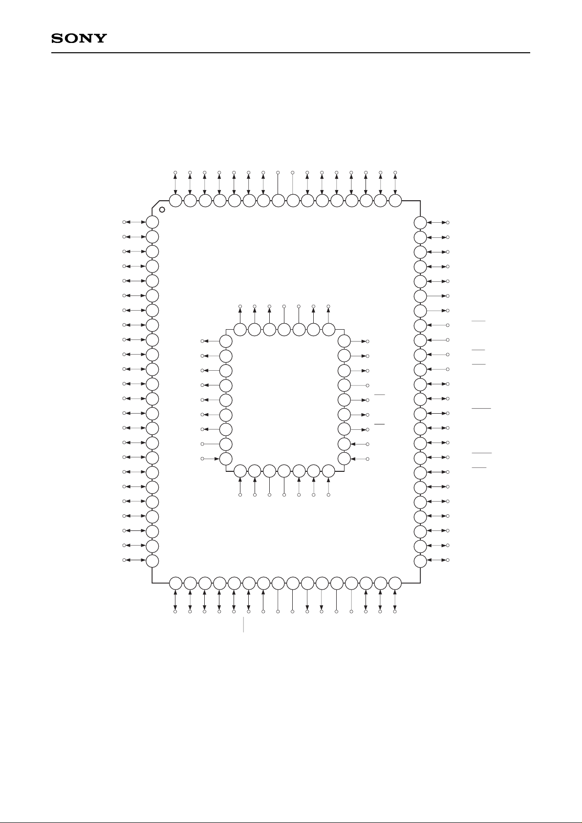
Pin Assignment in Piggyback Mode
Note) NC (pin 73) is left open.
However, this pin is used for the Flash EEPROM incorporated version (CXP845F60).
A8
A9
A11
NC
OE
A10
CE
D7
D6
A6
A5
A4
A3
A2
A1
A0
NC
D0
A7
A12
A15
NC
V
DD
A14
A13
D1
D2
GND
NC
D3
D4
D5
2
3
4
5
6
7
8
9
10
11
12
13
14 15
16
17
18
19
20
21
22
23
24
25
26
27
28
29
30
31
32
1
PF3
PF4
PF5
PF6
PF7
PD0
PD1
PD2
PD3
PD4
PD5
PD6
PD7
PC0
PC1
PC2
PC3
PC4
PC5
PC6
PC7
PH0
PH1
PH2
PI4
PI3/INT3
PI2/INT2
PI1/INT1
PI0/INT0
PE5/TO/PWM1
PE4/PWM0
PE3/NMI
PE2/CINT
PE1/EC1
PE0/EC0
PB7/SO1
PB6/SI1
PB5/SCK1
PB4/SO0
PB3/SI0
PB2/SCK0
PB1/CS0
PB0/LAT0
PA7/AN7
PA6/AN6
PA5/AN5
PA4/AN4
PA3/AN3
PH3
PH4
PH5
PH6
PH7
RST
EXTAL
XTAL
V
SS
PE6
PE7
AV
SS
AV
REF
PA0/AN0
PA1/AN1
PA2/AN2
PF2
PF1
PF0
PG7
PG6
PG5
PG4
NC
V
DD
PG3
PG2
PG1
PG0
PI7
PI6
PI5
2
3
4
5
6
7
8
9
10
11
12
13
14
15
16
17
18
19
20
21
22
23
24
25
26
27
28
29
30
40
39
38
37
36
35
34
31
32
33
41
42
43
44
45
46
47
48
49
50
51
52
53
54
55
56
57
58
59
60
70
69
68
67
63
64
65
66
61
62
71
72
73
74
75
76
77
78
79
80
1
 Loading...