

Sony CXP84224, CXP84220 Datasheet

Description
The CXP84220/84224 is a CMOS 8-bit single chip
microcomputer integrating on a single chip an A/D
converter, serial interface, timer/counter, time base
timer, capture timer counter, remote control reception
circuit besides the basic configurations of 8-bit CPU,
ROM, RAM, and l/O port.
The CXP84220/84224 also provides a power-on
reset function and a sleep/stop function that enables
lower power consumption.
Features
• Wide-range instruction system (213 instructions) to cover various types of data
—16-bit arithmetic/multiplication and division/Boolean bit operation instructions
• Minimum instruction cycle 400ns at 10MHz operation
• Incorporated ROM capacity 20K bytes (CXP84220)
24K bytes (CXP84224)
• Incorporated RAM capacity 624 bytes
• Peripheral functions
—A/D converter 8-bit, 8-channel, successive approximation method
(Conversion time of 32µs/10MHz)
—Serial interface SIO with 8-bit, 8-stage FIFO incorporated for data use
(Auto transfer for 1 to 8 bytes), 1 channel
8-bit standard SIO, 1 channel
—Timer 8-bit timer, 8-bit timer/counter, 19-bit time base timer,
16-bit capture timer/counter
—Remote control reception circuit Incorporated noise elimination circuit
Incorporated 8-bit, 6-stage FIFO for measurement data
—PWM output circuit 14 bits, 1 channel
• Interruption 13 factors, 14 vectors, multi-interruption possible
• Standby mode Sleep/stop
• Package 64-pin plastic SDIP
• Piggyback/evaluation chip CXP84200 64-pin ceramic SDIP
Structure
Silicon gate CMOS IC
CMOS 8-bit Single Chip Microcomputer
– 1 –
E93236A81-PS
Sony reserves the right to change products and specifications without prior notice. This information does not convey any license by
any implication or otherwise under any patents or other right. Application circuits shown, if any, are typical examples illustrating the
operation of the devices. Sony cannot assume responsibility for any problems arising out of the use of these circuits.
CXP84220/84224
64 pin SDIP (Plastic)
8
2
2
2
2
PA0/AN0 to
PA7/AN7
PE4/PWM
PE2/RMC
PB1/CS0
PB3/SI0
PB4/SO0
PB2/SCK0
PB6/SI1
PB7/SO1
PB5/SCK1
PE5/TO
PB0/CINT
PE1/EC1
PE0/EC0
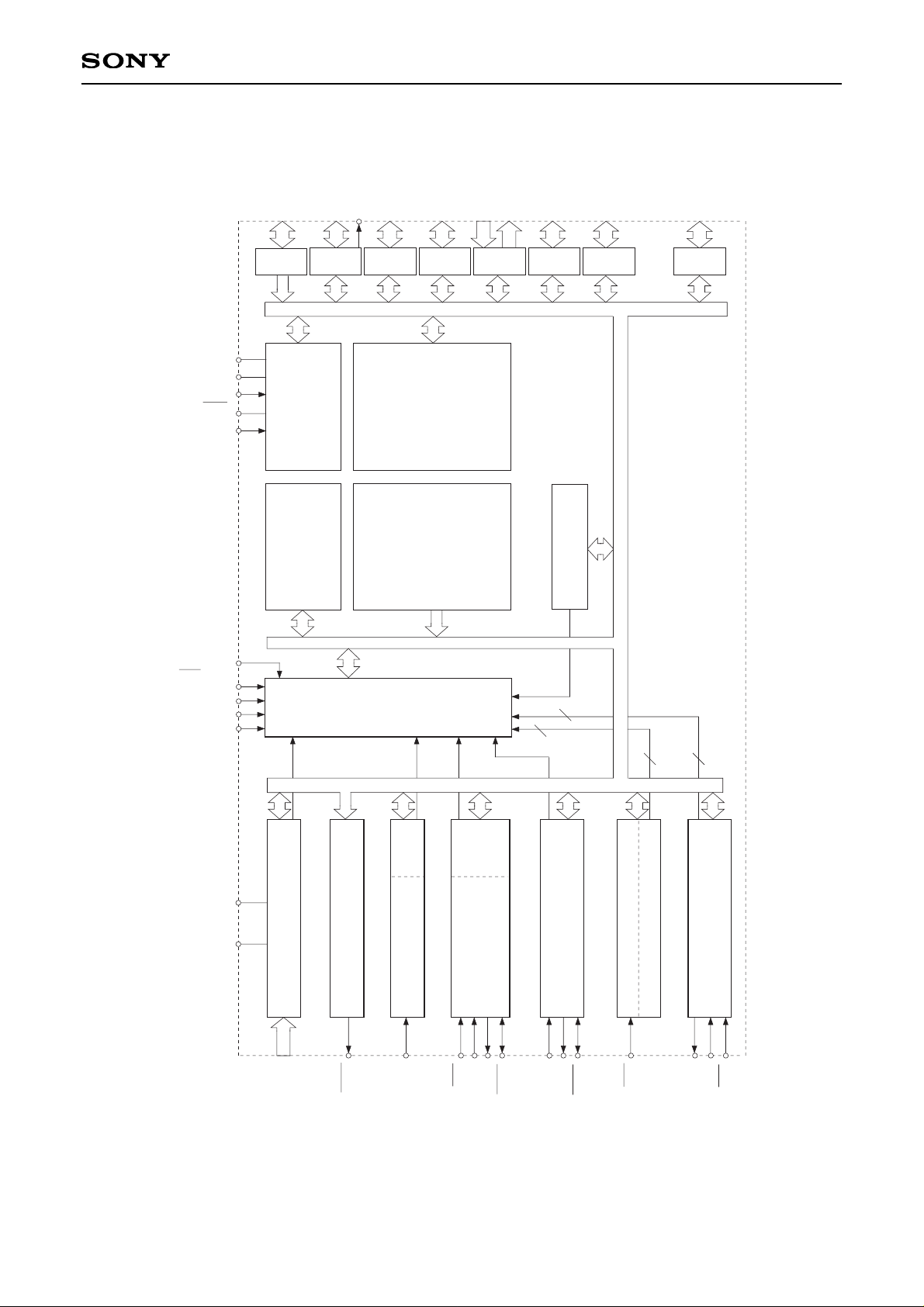
A/D CONVERTER
AVss
AV
REF
14 BIT PWM GENERATOR
REMOCON
FIFO
SERIAL
INTERFACE
UNIT 0
FIFO
SERIAL INTERFACE UNIT 1
8 BIT TIMER/COUNTER 0
8 BIT TIMER 1
16 BIT CAPTURE
TIMER/COUNTER 2
INTERRUPT CONTROLLER
PI0/INT0
PI1/INT1
PI2/INT2
PI3/INT3
PE3/NMI
SPC700
CPU CORE
ROM
20K/24K BYTES
CLOCK GEN./
SYSTEM CONTROL
RAM
624 BYTES
PRESCALER /
TIME BASE TIMER
EXTAL
XTAL
RST
V
DD
Vss
PORT A
7
8
8
4
2
7
PA0 to PA7
PB0 to PB6
PB7
PC0 to PC7
PD0 to PD7
PE0 to PE3
PE4 to PE5
PF0 to PF7
PG0 to PG2
PI0 to PI6
8
8
3
PORT B
PORT C
PORT D
PORT E
PORT F
PORT G
PORT I
– 2 –
CXP84220/84224
Block Diagram
NC
PG0
PG1
PG2
PF0
PF1
PF2
PF3
PF4
PF5
PF6
PF7
PD0
PD1
PD2
PD3
PD4
PD5
PD6
PD7
PC0
PC1
PC2
PC3
PC4
PC5
PC6
PC7
RST
XTAL
EXTAL
Vss
2
3
4
5
6
7
8
9
10
11
12
13
14
15
16
17
18
19
20
21
22
23
24
25
26
27
28
29
30
31
32
1
VDD
PI6
PI5
PI4
PI3/INT3
AV
REF
AVss
40
39
38
37
36
35
34
33
41
42
43
44
45
46
47
48
49
50
51
52
53
54
55
56
57
58
59
60
63
64
61
62
PI2/INT2
PI1/INT1
PI0/INT0
PE5/TO
PE4/PWM
PE3/NMI
PE2/RMC
PE1/EC1
PE0/EC0
PB7/SO1
PB6/SI1
PB5/SCK1
PB4/SO0
PB3/SI0
PB2/SCK0
PB1/CS0
PB0/CINT
PA7/AN7
PA6/AN6
PA5/AN5
PA4/AN4
PA3/AN3
PA2/AN2
PA1/AN1
PA0/AN0
– 3 –
CXP84220/84224
Pin Assignment (Top View)
Note) NC (Pin 1) is always connected to VDD.
– 4 –
CXP84220/84224
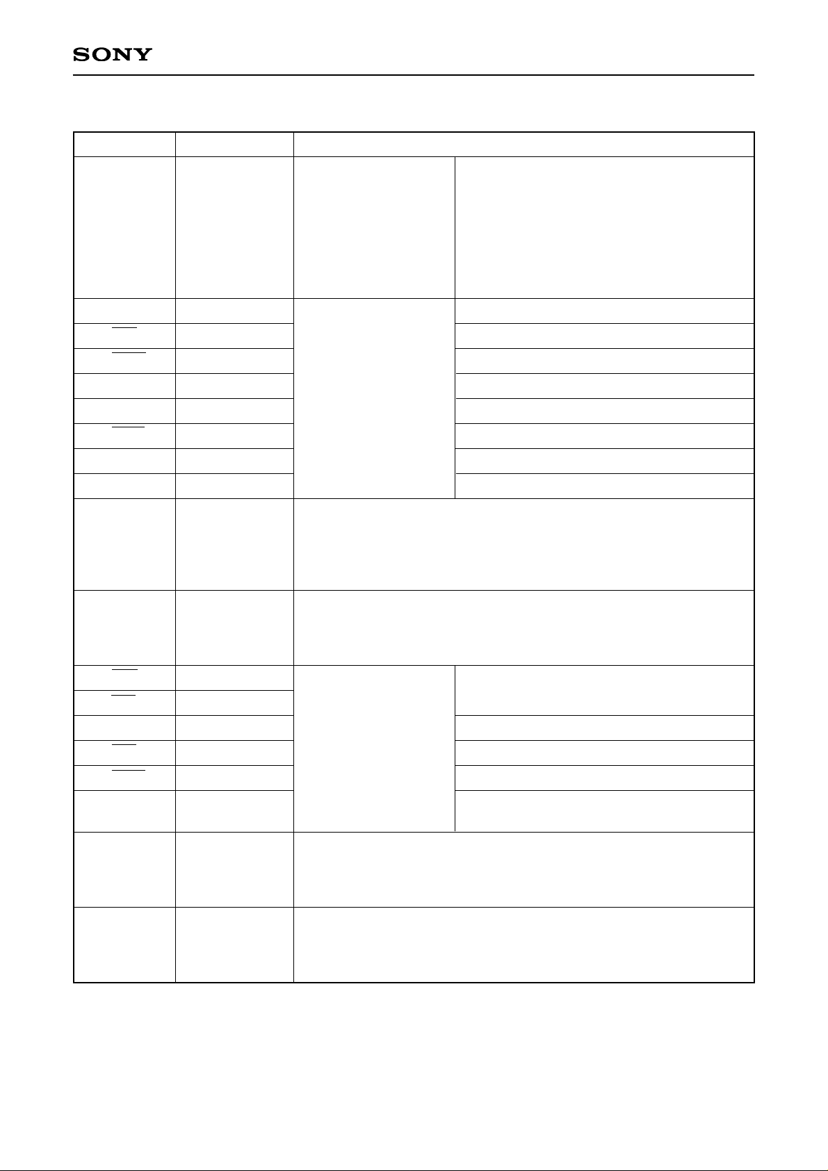
Pin Description
I/O/Analog input
PA0/AN0
to
PA7/AN7
(Port A)
8-bit l/O port. l/O can be
set in a unit of single bit.
Incorporation of the pullup resistance can be set
through the software in a
unit of 4 bits.
(8 pins)
Analog inputs to A/D converter.
(8 pins)
I/OPC0 to PC7
(Port C)
8-bit l/O port. l/O can be set in a unit of single bit. Capable of driving
12mA sink current. Incorporation of pull-up resistor can be set through
the software in a unit of 4 bits.
(8 pins)
I/OPD0 to PD7
(Port D)
8-bit l/O port. l/O can be set in a unit of single bits. Incorporation of pullup resistor can be set through the software in a unit of 4 bits.
(8 pins)
I/OPF0 to PF7
(Port F)
8-bit output port. I/O can be set in a unit of single bit. Incorporation of
pull-up resistor can be set through the software in a unit of 4 bits.
(8 pins)
I/OPG0 to PG2
(Port G)
8-bit I/O port. I/O can be set in a unit of single bit. Incorporation of pull-up
resistor can be set through the software in a unit of 4 bits.
(3 pins)
Input/Input
Input/Input
Input/Input
Input/Input
Output/Output
Output/Output
PE0/EC0
PE1/EC1
PE2/RMC
PE3/NMI
PE4/PWM
PE5/TO
(Port E)
6-bit port. Lower 4 bits
are for inputs; upper 2
bits are for outputs. (6
pins)
Remote control reception circuit input.
Non-maskable interruption request input.
14-bit PWM output.
Rectangular wave output for 16-bit
timer/counter.
I/O/Input
I/O/Input
I/O/I/O
I/O/Input
I/O/Output
I/O/I/O
I/O/Input
Output/Output
PB0/CINT
PB1/CS0
PB2/SCK0
PB3/SI0
PB4/SO0
PB5/SCK1
PB6/SI1
PB7/SO1
(Port B)
7-bit l/O port in which
l/O can be set in a unit
of single bit. Also, an
uppermost bit (PB7)
exclusively for output.
Incorporation of pull-up
resistor can be set
through the software in
a unit of 4 bits.
(8 pins)
External capture input to 16-bit timer/counter.
Chip select input for serial interface (CH0).
Serial clock l/O (CH0).
Serial data input (CH0).
Serial data output (CH0).
Serial clock l/O (CH1).
Serial data input (CH1).
Serial data output (CH1).
Pin code I/O Description
External event inputs for timer/counter.
(2 pins)
– 5 –
CXP84220/84224
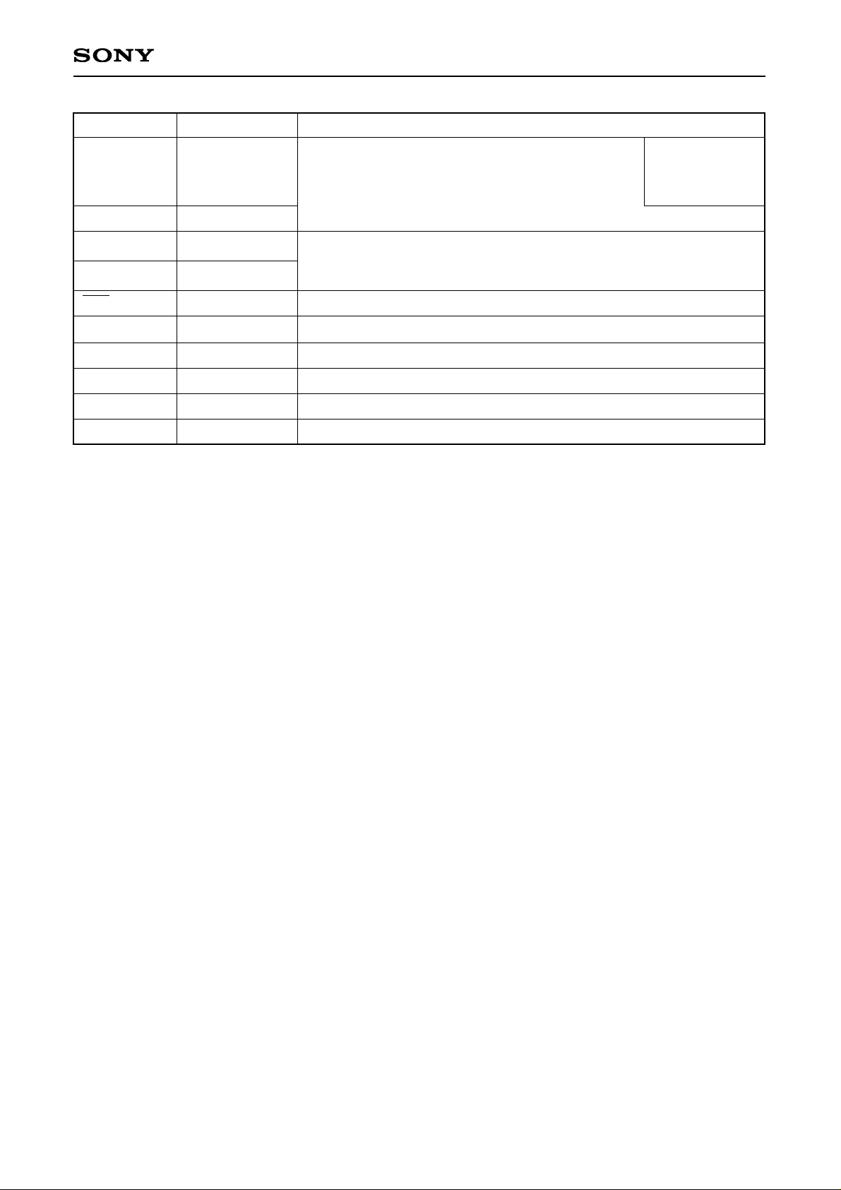
Pin code
I/O
Description
I/O/Input
PI0/INT0
to
PI3/INT3
I/O
PI4 to PI6
Input
Crystal connectors for system clock oscillation. When the clock is
supplied externally, input to EXTAL; opposite phase clock should be
input to XTAL.
EXTAL
Output
XTAL
I/O
Low-level active, system reset.
RST
NC. Under normal operating conditions, connect to VDD.
NC
Input
Reference voltage input for A/D converter.
AVREF
A/D converter GND.
AVss
Positive power supply.
VDD
GND
Vss
(Port l)
7-bit output ports. I/O can be set in a unit of single bit.
Incorporation of pull-up resistor can be set through
the software in a unit of 4 bits.
(7 pins)
External
interruption
request inputs.
– 6 –
CXP84220/84224
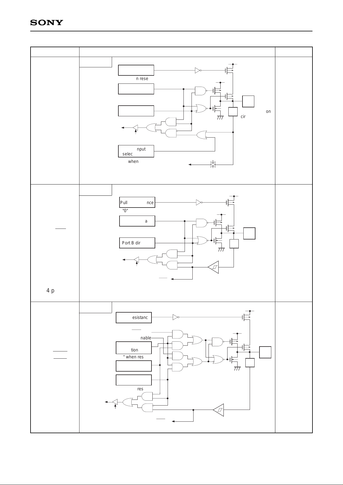
Input/Output Circuit Formats for Pins
Port B
Data bus
RD (Port B)
Port B direction
IP
Port B data
Pull-up resistance
"0" when reset
"0" when reset
∗
Pull-up transistors
approx. 10kΩ
∗
Schmitt input
CINT
CS0
SI0
SI1
8 pins
Hi-Z
Hi-Z
When reset
PA0/AN0
to
PA7/AN7
PB0/CINT
PB1/CS0
PB3/SI0
PB6/SI1
Port B
Data bus
RD (Port B)
IP
Port B output
selection
"0" when reset
∗
Pull-up transistors
approx. 10kΩ
∗
Schmitt input
SCK in
Port B data
Port B direction
"0" when reset
Pull-up resistance
"0" when reset
SCK OUT
Output enable
4 pins
2 pins
Hi-Z
PB2/SCK0
PB5/SCK1
Data bus
RD (Port A)
Port A direction
IP
Port A data
Pull-up resistance
Port A input
selection
Input protection
circuit
"0" when reset
"0" when reset
"0" when reset
Input multiplexer
A/D converter
∗
Pull-up transistors
approx. 10kΩ
∗
Port A
Pin
Circuit format
 Loading...