

Sony CXP83625, CXP83624, CXP83621, CXP83620 Datasheet
CMOS 8-bit Single Chip Microcomputer
Description
The CXP83620/83624 and the CXP83621/83625
are CMOS 8-bit single chip microcomputer integrating
on a single chip an A/D converter, serial interface,
timer/counter, time-base timer, sub timer/counter, LCD
controller/driver and remote control reception circuit
besides the basic configurations of 8-bit CPU, ROM,
RAM, and I/O port.
The CXP83620/83624 and the CXP83621/83625 also
provide a sleep/stop function that enables lower power
consumption.
Features
• Wide-range instruction system (213 instructions) to
cover various types of data.
— 16-bit arithmetic/multiplication and division/boolean
bit operation instructions
• Minimum instruction cycle
400ns at 10MHz operation (4.5 to 5.5V)
1µs at 4MHz operation (2.7 to 5.5V)
122µs at 32kHz operation (2.7 to 5.5V)
• Incorporated ROM capacity
20K bytes (CXP83620, 83621)
24K bytes (CXP83624, 83625)
• Incorporated RAM capacity
736 bytes (includes LCD display data area and serial interface RAM)
• Peripheral functions
— A/D converter 8-bit, 8-channel, successive approximation method
(Conversion time of 12.4µs/10MHz)
— Serial interface Incorporated buffer RAM
(Auto transfer for 1 to 32 bytes), 1 channel
8-bit clock synchronized type (MSB/LSB first selectable), 1 channel
— Timer 8-bit timer, 8-bit timer/counter, 19-bit time-base timer,
Sub timer/counter
— LCD controller/driver Maximum 128 segment display possible (during 1/4 duty)
4 common output, 32 segment output
Display method static, 1/2, 1/3, 1/4 duty
Bias method 1/2, 1/3 bias
— Remote control reception circuit 8-bit pulse measuring counter, 6-stage FIFO
• Interruption 14 factors, 14 vectors, multi-interruption possible
• Standby mode Sleep/stop
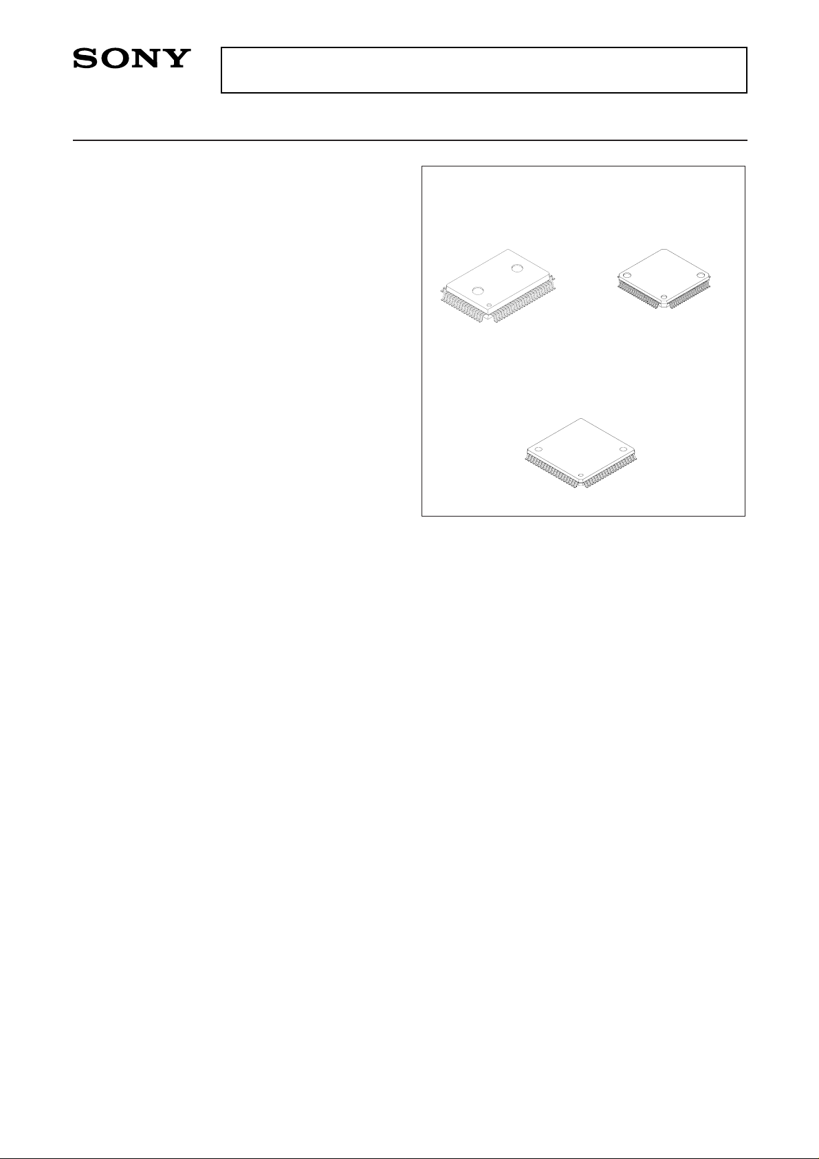
• Package 80-pin plastic QFP/LQFP
• Piggy/evaluation chip CXP83600 (CXP83620, 83624)
CXP83601 (CXP83621, 83625)
Structure
Silicon gate CMOS IC
– 1 –
E98134B96
Sony reserves the right to change products and specifications without prior notice. This information does not convey any license by
any implication or otherwise under any patents or other right. Application circuits shown, if any, are typical examples illustrating the
operation of the devices. Sony cannot assume responsibility for any problems arising out of the use of these circuits.
CXP83620/83624
CXP83621/83625
CXP83620/83624
80 pin QFP (Plastic) 80 pin LQFP (Plastic)
CXP83621/83625
80 pin QFP (Plastic)
– 2 –
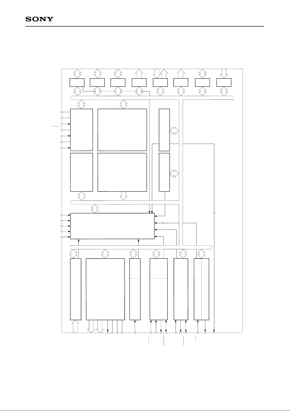
CXP83620/83624, CXP83621/83625
XTAL
A/D CONVERTER
REMOCON
SERIAL
INTERFACE
UNIT (CH0)
8-BIT TIMER/COUNTER 0
8-BIT TIMER 1
FIFO
BUFFER
RAM
INTERRUPT CONTROLLER
SPC700
CPU CORE
ROM
20K/24K BYTES
PRESCALER/
TIME-BASE TIMER
SUB TIMER/
COUNTER
RAM
736 BYTES
8
AN0 to AN7
RMC
SI0
SO0
SI1
SO1
EC
CS0
SCK0
SCK1
INT0
INT1
INT2
INT3
TEX
TX
EXTAL
V
DD
Vss
PORT C
8
PC0 to PC7
PORT H
1
PH0
PORT B
8
PB0 to PB7
PORT E
5
2
PE0 to PE4
PE5 to PE6
2
LCD
CONTROLLER/
DRIVER
32
SEG0 to SEG31
4
COM0 to COM3
VL
VLC1
VLC2
PORT A
8
PA0 to PA7
PORT D
8
PD0 to PD7
PORT F
8
PF0 to PF7
VLC3
ADJ
TO
CLOCK GENERATOR/
SYSTEM CONTROL
RST
3
INT4
PORT I
2
PI0 to PI1
SERIAL INTERFACE UNIT
(CH1)
Block Diagram
– 3 –
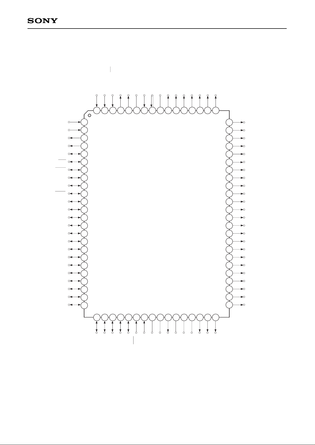
CXP83620/83624, CXP83621/83625
PE3/INT3
PE4/RMC
PE5/TO
PE6/ADJ
PB0
PB1/CS0
PB2/SCK0
PB3/SI0
PB4/SO0
PB5/SCK1
PB6/SI1
PB7/SO1
PC0
PC1
PC2
PC3
PC4
PC5
PC6
PC7
PH0/INT4
PA0/AN0
PA1/AN1
PA2/AN2
PD6/SEG22
PD5/SEG21
PD4/SEG20
PD3/SEG19
PD2/SEG18
PD1/SEG17
PD0/SEG16
SEG15
SEG14
SEG13
SEG12
SEG11
SEG10
SEG9
SEG8
SEG7
SEG6
SEG5
SEG4
SEG3
SEG2
SEG1
SEG0
COM3
PA3/AN3
PA4/AN4
PA5/AN5
PA6/AN6
PA7/AN7
RST
EXTAL
XTAL
V
SS
V
L
V
LC3
V
LC2
V
LC1
COM0
COM1
COM2
PE2/INT2
PE1/INT1
PE0/INT0/EC
PF7/SEG31
PF6/SEG30
NC
PI1/TEX
PI0/TX
V
DD
PF5/SEG29
PF4/SEG28
PF3/SEG27
PF2/SEG26
PF1/SEG25
PF0/SEG24
PD7/SEG23
2
3
4
5
6
7
8
9
10
11
12
13
14
15
16
17
18
19
20
21
22
23
24
25
26
27 28
29
30
40
39
38
37
36
35
34
31
32
33
70
69
68
67
65
66
71
72
73
74
75
76
77
78
79
80
1
41
42
43
44
45
46
47
48
49
50
51
52
53
54
55
56
57
58
59
60
63
64
61
62
Note) Do not make any connections to NC (Pin 75).
Pin Assignment (Top View) CXP83620/83624 (QFP package)

– 4 –
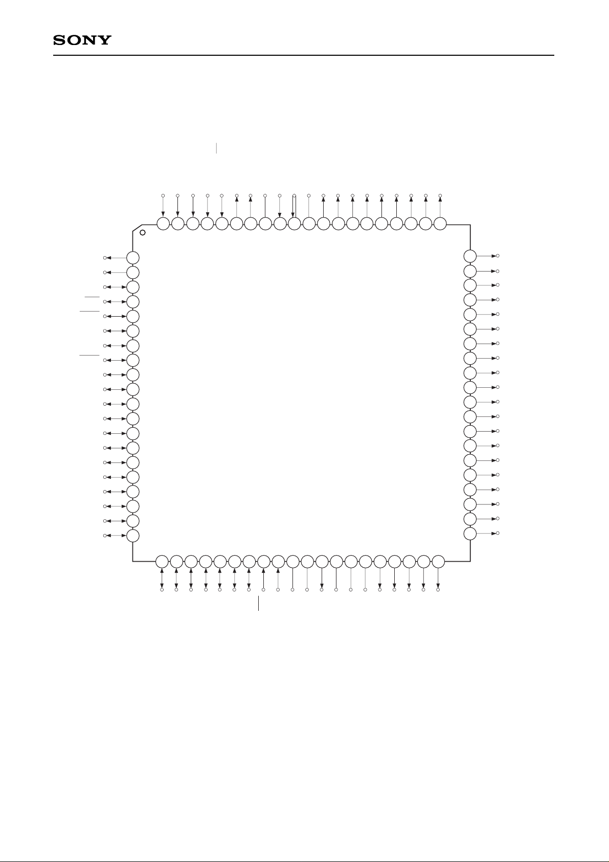
CXP83620/83624, CXP83621/83625
Pin Assignment (Top View) CXP83620/83624 (LQFP package)
PE5/TO
PE6/ADJ
PB0
PB1/CS0
PB2/SCK0
PB3/SI0
PB4/SO0
PB5/SCK1
PB6/SI1
PB7/SO1
PC0
PC1
PC2
PC3
PC4
PC5
PC6
PC7
PH0/INT4
PA0/AN0
PD4/SEG20
PD3/SEG19
PD2/SEG18
PD1/SEG17
PD0/SEG16
SEG15
SEG14
SEG13
SEG12
SEG11
SEG10
SEG9
SEG8
SEG7
SEG6
SEG5
SEG4
SEG3
SEG2
SEG1
PA1/AN1
PA2/AN2
PA3/AN3
PA4/AN4
PA5/AN5
PA6/AN6
PA7/AN7
RST
EXTAL
XTAL
V
SS
V
L
V
LC3
V
LC2
V
LC1
COM0
COM1
COM2
COM3
SEG0
PE4/RMC
PE3/INT3
PE2/INT2
PE1/INT1
PE0/INT0/EC
PF7/SEG31
PF6/SEG30
NC
PI1/TEX
PI0/TX
V
DD
PF5/SEG29
PF4/SEG28
PF3/SEG27
PF2/SEG26
PF1/SEG25
PF0/SEG24
PD7/SEG23
PD6/SEG22
PD5/SEG21
2
3
4
5
6
7
8
9
10
11
12
13
14
15
16
17
18
19
20
21
22
23
24
25
26
27
28
29
30
40
39
38
37
36
35
34
31
32
33
70
69
68
67
65
66
71
72
73
74
75
76
77
78
79
80
1
41
42
43
44
45
46
47
48
49
50
51
52
53
54
55
56
57
58
59
60
63
64
61
62
Note) Do not make any connections to NC (Pin 73).
– 5 –
CXP83620/83624, CXP83621/83625
Pin Assignment (Top View) CXP83621/83625 (QFP package)
PE5/TO
PE6/ADJ
PB0
PB1/CS0
PB2/SCK0
PB3/SI0
PB4/SO0
PB5/SCK1
PB6/SI1
PB7/SO1
PC0
PC1
PC2
PC3
PC4
PC5
PC6
PC7
PH0/INT4
PA0/AN0
PD4/SEG20
PD3/SEG19
PD2/SEG18
PD1/SEG17
PD0/SEG16
SEG15
SEG14
SEG13
SEG12
SEG11
SEG10
SEG9
SEG8
SEG7
SEG6
SEG5
SEG4
SEG3
SEG2
SEG1
PA1/AN1
PA2/AN2
PA3/AN3
PA4/AN4
PA5/AN5
PA6/AN6
PA7/AN7
RST
EXTAL
XTAL
V
SS
V
L
V
LC3
V
LC2
V
LC1
COM0
COM1
COM2
COM3
SEG0
PE4/RMC
PE3/INT3
PE2/INT2
PE1/INT1
PE0/INT0/EC
PF7/SEG31
PF6/SEG30
NC
PI1/TEX
PI0/TX
V
DD
PF5/SEG29
PF4/SEG28
PF3/SEG27
PF2/SEG26
PF1/SEG25
PF0/SEG24
PD7/SEG23
PD6/SEG22
PD5/SEG21
2
3
4
5
6
7
8
9
10
11
12
13
14
15
16
17
18
19
20
21
22
23
24
25
26
27
28
29
30
40
39
38
37
36
35
34
31
32
33
70
69
68
67
65
66
71
72
73
74
75
76
77
78
79
80
1
41
42
43
44
45
46
47
48
49
50
51
52
53
54
55
56
57
58
59
60
63
64
61
62
Note) Do not make any connections to NC (Pin 73).
– 6 –
CXP83620/83624, CXP83621/83625
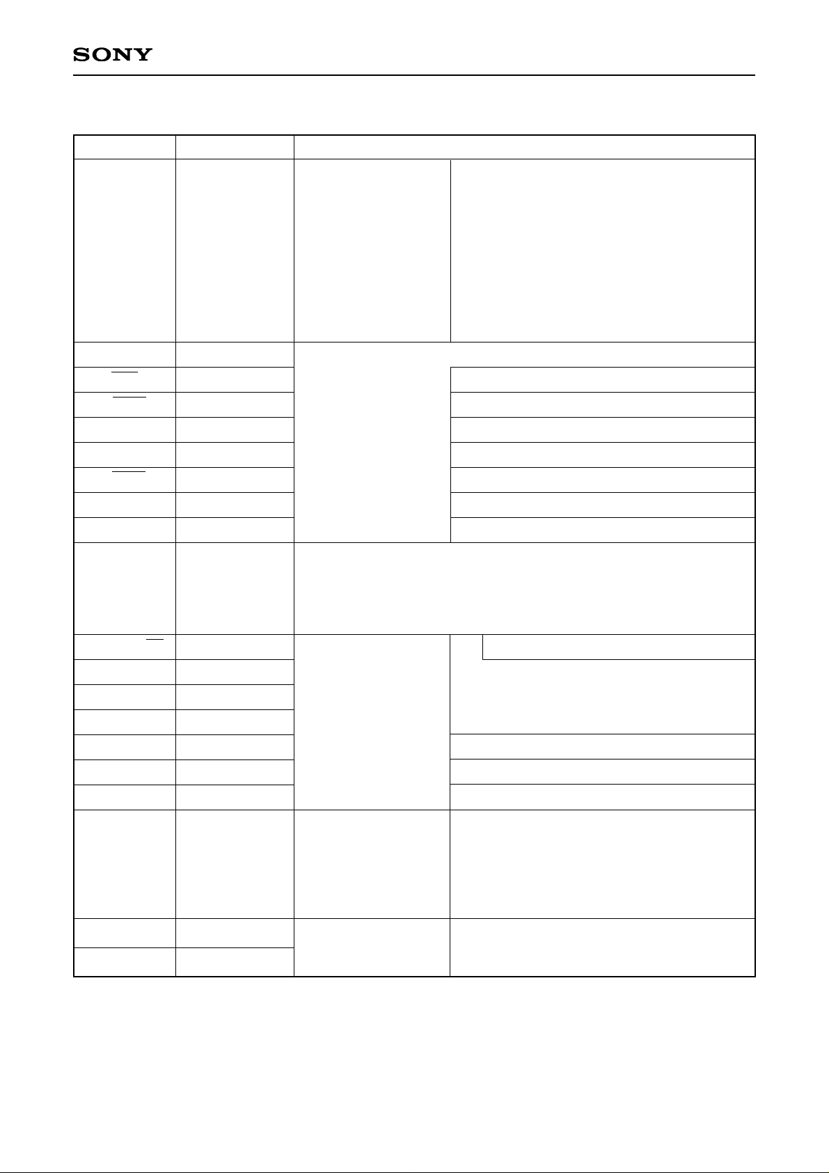
Pin Description
Symbol I/O Functions
I/O/Analog input
PA0/AN0
to
PA7/AN7
(Port A)
8-bit I/O port. I/O can
be set in a bit unit.
Standby release input
can be set in a bit unit.
Incorporation of pull-up
resistor can be set
through the program in
a bit unit.
(8 pins)
Analog inputs to A/D converter.
(8 pins)
I/O
PC0 to PC7
PE0/INT0/EC
PE1/INT1
PE2/INT2
PE3/INT3
PE4/RMC
PE5/TO
PE6/ADJ
PH0/INT4
PI0/TX
PI1/TEX
Input/Input/Input
Input/Input
Input/Input
Input/Input
Input/Input
Output/Output
Output/Output
I/O/Input
Input
Input/Input
(Port C)
8-bit I/O port. I/O can be set in a bit unit. Capable of driving 12mA sink
current. Incorporation of pull-up resistor can be set through the program
in a bit unit.
(8 pins)
(Port E)
7-bit port. Lower 5 bits
are for inputs; upper 2
bits are for outputs.
(7 pins)
(Port H)
1-bit I/O port.
Incorporation of pull-up
resistor can be set
through the program.
(1 pin)
(Port I)
2-bit input port.
(2 pins)
External interruption request input.
(1 pin)
Crystal connectors for sub timer/counter clock
oscillation. For usage as event counter, input to
TEX, and leave TX open.
External event inputs for 8-bit timer/counter.
External interruption request inputs.
(4 pins)
Remote control reception circuit input.
Output for 8-bit timer/counter rectangular wave.
Output for TEX oscillation frequency division.
I/O
I/O/Input
I/O/I/O
I/O/Input
I/O/Output
I/O/I/O
I/O/Input
I/O/Output
PB0
PB1/CS0
PB2/SCK0
PB3/SI0
PB4/SO0
PB5/SCK1
PB6/SI1
PB7/SO1
(Port B)
8-bit I/O port. I/O can
be set in a bit unit.
Incorporation of pull-up
resistor can be set
through the program in
a bit unit.
(8 pins)
Chip select input for serial interface (CH0).
Serial clock I/O (CH0).
Serial data input (CH0).
Serial data output (CH0).
Serial clock I/O (CH1).
Serial data input (CH1).
Serial data output (CH1).
– 7 –
CXP83620/83624, CXP83621/83625
Symbol I/O Functions
Output/Output
PF0/SEG24
to
PF7/SEG31
(Port F)
8-bit output port.
(8 pins)
Output/Output
PD0/SEG16
to
PD7/SEG23
(Port D)
8-bit output port.
(8 pins)
Output
SEG0 to SEG15
LCD segment signal output. (16 pins)
Input
Crystal connectors for system clock oscillation. When the clock is supplied
externally, input to EXTAL; opposite phase clock should be input to XTAL.
EXTAL
Output
COM0 to COM3 LCD common signal output. (4 pins)
VLC1 to VLC3
LCD bias power supply. (3 pins)
Output
VL
Control pin to cut off the current flowing to external LCD bias resistor
during standby.
XTAL
Input
Low-level active system reset.
NC. Do not make any connections to NC.
Positive power supply.
GND.
RST
NC
VDD
VSS
LCD segment signal outputs.
(16 pins)
– 8 –
CXP83620/83624, CXP83621/83625
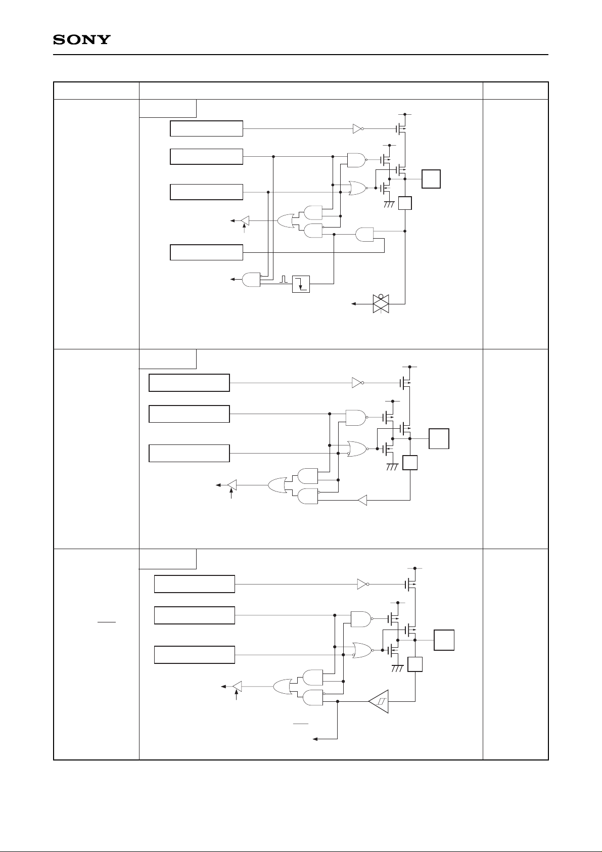
∗
Pull-up transistor
approx. 100kΩ (VDD = 4.5 to 5.5V)
approx. 150kΩ (VDD = 2.7 to 3.3V)
IP
Pull-up resistor
Port B data
Port B direction
"0" after a reset
RD (Port B)
"0" after a reset
∗
Internal data bus
∗
Pull-up transistor
approx. 100kΩ (VDD = 4.5 to 5.5V)
approx. 150kΩ (VDD = 2.7 to 3.3V)
IP
Pull-up resistor
Port B data
Port B direction
"0" after a reset
RD (Port B)
"0" after a reset
∗
Internal data bus
CS0
SI0
SI1
Schmitt input
Port B
8 pins
Hi-Z
Hi-Z
After a reset
PA0/AN0
to
PA7/AN7
PB0
Port B
1 pin
3 pins
Hi-Z
PB1/CS0
PB3/SI0
PB6/SI1
∗
Pull-up transistor
approx. 100kΩ (VDD = 4.5 to 5.5V)
approx. 150kΩ (VDD = 2.7 to 3.3V)
IP
Pull-up resistor
Port A data
Port A direction
"0" after a reset
Port A function select
"0" after a reset
RD (Port A)
A/D converter
Input multiplexer
"0" after a reset
Input protection
circuit
∗
Edge detection
circuit
Internal data bus
Standby release
I/O Circuit Format for Pins
Port A
Pin
Circuit format
– 9 –
CXP83620/83624, CXP83621/83625
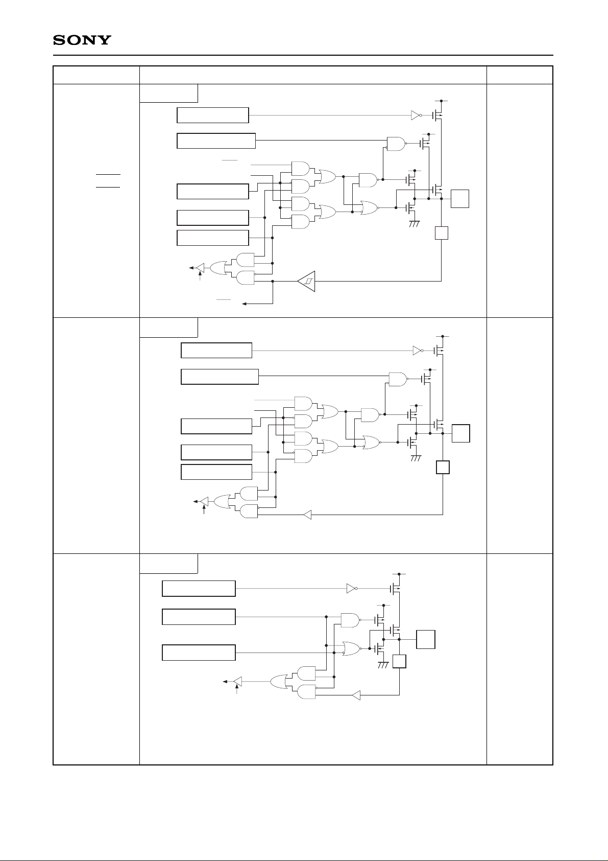
Port B
Port C
2 pins
Hi-Z
Hi-Z
After a reset
PB2/SCK0
PB5/SCK1
PB4/SO0
PB7/SO1
2 pins
Hi-Z
PC0 to PC7
8 pins
Pull-up resistor
"0" after a reset
RD (Port B)
∗
"0" after a reset
Schmitt input
SCK in
Internal
data bus
Port B data
Port B direction
IP
Serial clock output ebable
Port B function select
"0" after a reset
SCK out
"0" after a reset
∗
Pull-up transistor
approx. 100kΩ (VDD = 4.5 to 5.5V)
approx. 150kΩ (VDD = 2.7 to 3.3V)
Output buffer capability
Port B
Pin
Circuit format
IP
Pull-up resistor
Port C data
Port C direction
"0" after a reset
RD (Port C)
"0" after a reset
∗
2
Internal data bus
∗
1
∗2
Pull-up transistor
approx. 100kΩ (VDD = 4.5 to 5.5V)
approx. 150kΩ (VDD = 2.7 to 3.3V)
∗
1
High current drive
12mA (VDD = 4.5 to 5.5V)
4.5mA (VDD = 2.7 to 3.3V)
Pull-up resistor
"0" after a reset
Output buffer capability
"0" after a reset
Serial data output ebable
Port B function select
"0" after a reset
Port B data
Port B direction
"0" after a reset
Internal
data bus
RD (Port B)
SO
∗
IP
∗
Pull-up transistor
approx. 100kΩ (VDD = 4.5 to 5.5V)
approx. 150kΩ (VDD = 2.7 to 3.3V)
 Loading...