

Sony CXK5T16100TM-12LLX Datasheet
CXK5T16100TM-12LLX
For the availability of this product, please contact the sales office.
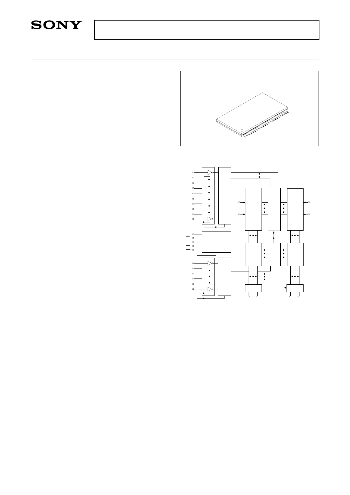
65536-word × 16-bit High Speed CMOS Static RAM
Description
The CXK5T16100TM is a general purpose high
speed CMOS static RAM organized as 65536words by 16-bits.
Special feature are low power consumption and
high speed.
The CXK5T16100TM is a suitable RAM for portable
equipment with battery back up.
Features
• Extended operating temperature range: –25 to +85°C
• Wide supply voltage range operation: 2.7 to 3.6V
• Fast access time: (Access time)
3.0V operation 120ns (max.)
3.3V operation 100ns (max.)
• Low power consumption operation:
Standby / DC operation
1.6µW (typ.) / 3.3mW (typ.)
100µW (max.) / 11mW (max.)
• Fully static memory ··· No clock or timing strobe
required
• Equal access and cycle time
• Common data input and output: three state output
• Directly LVTTL compatible: All inputs and outputs
• Low voltage data retention: 2.0V (min.)
• 400mil 44pin TSOP (type II) package
Block Diagram
A1
A0
A7
A6
A5
A4
A3
A2
A15
A14
CE
UB
LB
OE
WE
A13
A12
A11
A10
A9
A8
44 pin TSOP (PIastic)
Buffer
Control
Buffer
Vcc
GND
Preliminary
Memory
Matrix
512 × 1024
I/O Gate
Column
Decoder
I/O Buffer
I/O1 I/O8
Row
Decoder
Pre
Decoder
Memory
Matrix
512 × 1024
I/O Gate
Column
Decoder
I/O Buffer
I/O9 I/O16
Vcc
GND
Function
65536-word x 16-bit static RAM
Structure
Silicon gate CMOS IC
Sony reserves the right to change products and specifications without prior notice. This information does not convey any license by
any implication or otherwise under any patents or other right. Application circuits shown, if any, are typical examples illustrating the
operation of the devices. Sony cannot assume responsibility for any problems arising out of the use of these circuits.
– 1 –
PE96405-ST
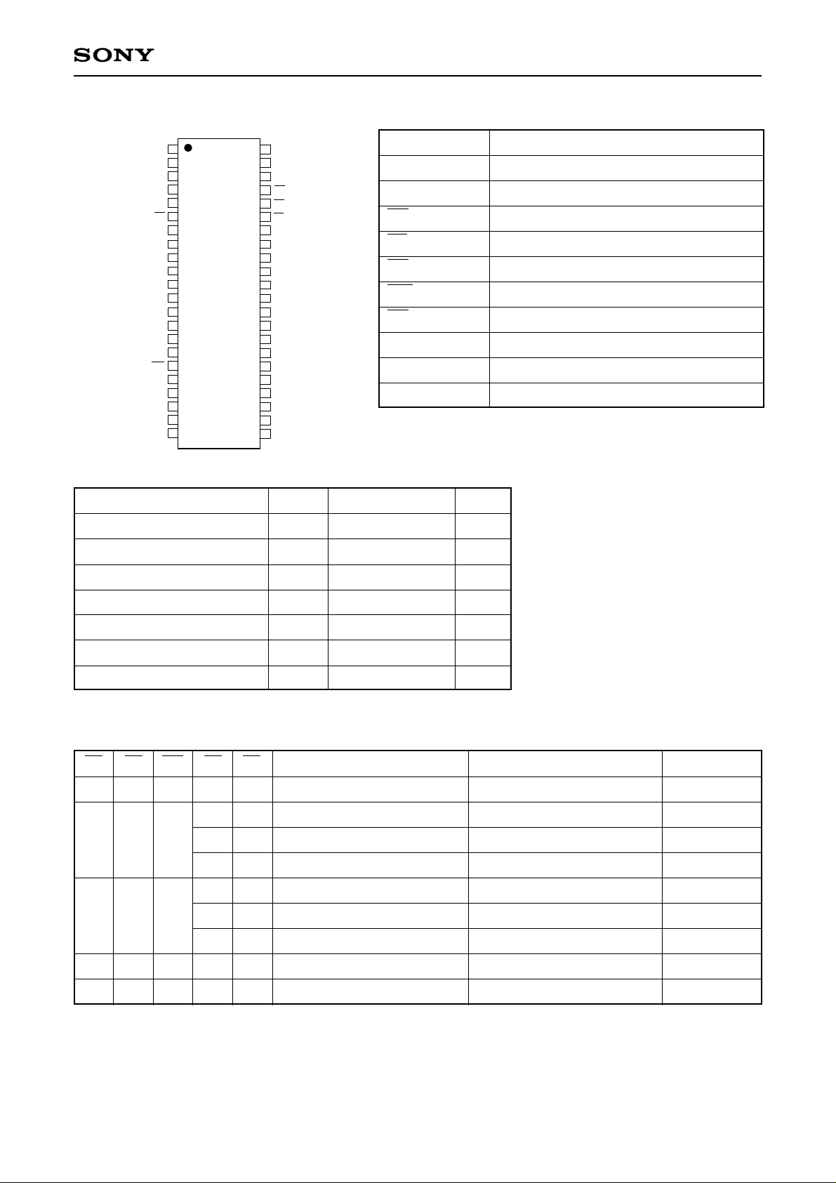
CE
I/O1
I/O2
I/O3
I/O4
Vcc
GND
I/O5
I/O6
I/O7
I/O8
WE
A15
A14
A13
A12
NC
CXK5T16100TM
Pin DescriptionPin Configuration (Top View)
1
A4
2
A3
3
A2
4
A1
5
A0
6
7
8
9
10
11
12
13
14
15
16
17
18
19
20
21
22
44
A5
43
A6
42
A7
41
OE
40
UB
39
LB
38
I/O16
37
I/O15
36
I/O14
35
I/O13
34
GND
33
Vcc
32
I/O12
31
I/O11
30
I/O10
29
I/O9
28
NC
27
A8
26
A9
25
A10
24
A11
23
NC
Symbol
A0 to A15
I/O1 to I/O16
CE
LB
UB
WE
OE
VCC
GND
NC
Address input
Data input/output
Chip enable input
Byte enable input (I/O1 to I/O8)
Byte enable input (I/O9 to I/O16)
Write enable input
Output enable input
Power supply
Ground
No connection
Description
Absolute Maximum Ratings (Ta = 25°C, GND = 0V)
Item Symbol Rating Unit
Supply voltage
Input voltage
Input and output voltage
Allowable power dissipation
Operating temperature
Storage temperature
Soldering temperature · time
∗1
VIN, VI/O = –3.0V Min. for pulse width less than 50ns.
VCC
VIN
VI/O
PD
Topr
Tstg
Tsolder
–0.5 to +4.6
–0.5∗1to VCC + 0.5
–0.5∗1to VCC + 0.5
0.7
–25 to +85
–55 to +150
235 · 10
V
V
V
W
°C
°C
°C · s
Truth Table
CE
OE WE LB UB I/O1 to I/O8 I/O9 to I/O16 Vcc Current
H
×
×
×
L
L
L
H
L
H
×
L
H
L
Not selected
Read
Read
High-Z
Not selected
Read
High-Z
Read
ISB1, ISB2
ICC1, ICC2, ICC3
ICC1, ICC2, ICC3
ICC1, ICC2, ICC3
L
×
L
H
L
×
×: “H” or “L”
L
L
L
H
H
×
×
H
Write
L
Write
H
Not Write/Hi-Z
L
High-Z
×
High-Z
H
Write
Not Write/Hi-Z
Write
High-Z
High-Z
ICC1, ICC2, ICC3
ICC1, ICC2, ICC3
ICC1, ICC2, ICC3
ICC1, ICC2, ICC3
ICC1, ICC2, ICC3
– 2 –
CXK5T16100TM
DC Recommended Operating Conditions (Ta = –25 to +85°C, GND = 0V)
Item
Supply voltage
Input high voltage
Input low voltage
∗1
VIL=–3.0V Min. for pulse width less than 50ns.
Symbol
VCC
VIH
VIL
VCC = 2.7 to 3.6V VCC = 3.3V ± 0.3V
Min.
2.7
2.4
–0.3
∗1
Typ. Max.
3.3
—
—
3.6
VCC + 0.3
0.4
Min. Typ. Max.
3.0
2.0
∗1
–0.3
3.3
—
—
3.6
VCC + 0.3
0.8
Unit
V
Electrical Characteristics
DC and operating characteristics (VCC = 2.7 to 3.6V, GND = 0V, Ta = –25 to +85°C)
—
—
∗2
Max. UnitTest condition
1
1
1
3
µA
µA
mA
Item Symbol Min. Typ.
Input leakage
current
Output leakage
current
Operating
power supply
current
ILI
ILO
ICC1
VIN = GND to VCC
CE = VIH or UB = VIH or LB = VIH or
OE = VIH or WE = VIL
VI/O = GND to VCC
CE = VIL
VIN = VIH or VIL
IOUT = 0mA
–1
–1
—
Min. cycle
ICC2
Duty = 100%
—
35
50
mA
IOUT = 0mA
Average
operating current
Standby current
Output
high voltage
Output
low voltage
∗2
VCC = 3.3V, Ta = 25°C
ICC3
ISB1
ISB2
VOH
VOL
Cycle time 1µs
Duty = 100%
IOUT = 0mA
CE ≤ 0.2V
VIL ≤ 0.2V
VIH ≥ VCC – 0.2V
CE ≥ VCC – 0.2V
CE = VIH
IOH = –2.0mA
IOL = 2.0mA
–25 to +85°C
–25 to +70°C
+25°C
—
—
—
—
—
2.4
—
10
—
—
0.48
0.03
—
—
20
28
14
—
0.6
—
0.4
mA
µA
mA
V
V
– 3 –
 Loading...