

Page 1
CFD-V3/V7/V7L
SERVICE MANUAL
Ver 1.5 2003.12
With SUPPLEMENT-1
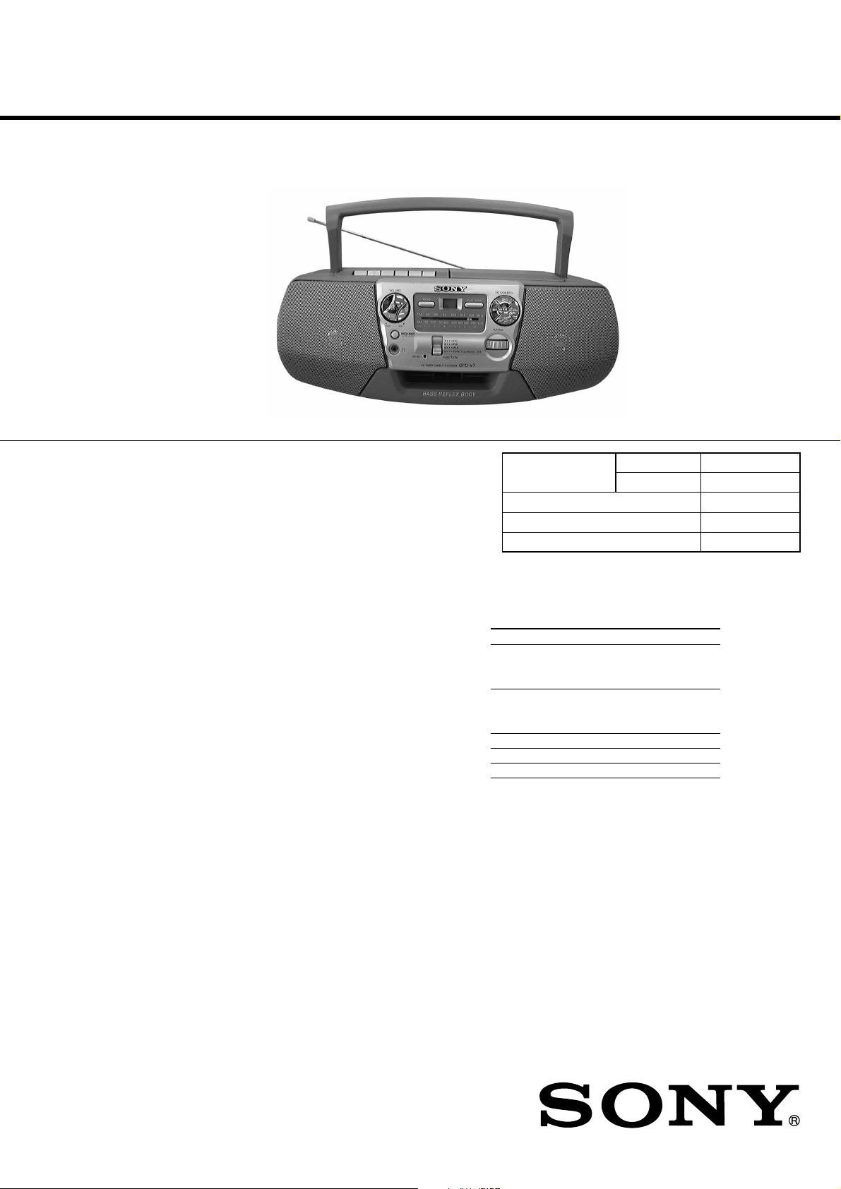
Photo : CFD–V7
Canadian Model
UK Model
Australian Model
CFD-V7
AEP Model
CFD-V3/V7/V7L
E Model
CFD-V3/V7
Model Name Using CD Section CFD-S36
Similar Mechanism Tape Section CFD-S36
CD Mechanism Type KSM-213CDP
Optical Pick-up Type KSS-213C
Tape Transport Mechanism T ype MF-V5-117
CD player section
System
Compact disc digital audio system
Laser diode properties
Material: GaAlAs
Wave length: 780 nm
Emission duration: Continuous
Laser output: Less than 44.6 µW
(This output is the value measured at a distance of about 200 mm
from the objective lens surface on the optical pick-up block with 7
mm aperture.)
Spindle speed
200 r/min (rpm) to 500 r/min (rpm) (CLV)
Number of channels
2
Frequency response
20 - 20 000 Hz +1/–2 dB
Wow and flutter
Below measurable limit
SPECIFICATIONS
Radio section
Frequency range
CFD-V3/V7
FM Italy 87.5 - 108 MHz
European countries 87.6 - 107 MHz
Other countries 87.6 - 108 MHz
AM Italy 526.5 - 1 606.5 kHz
European countries 531 - 1 602 kHz
Other countries 530 - 1 710 kHz
CFD-V7L
FM 87.6 - 107 MHz
LW 153 - 279 kHz
IF
FM: 10.7 MHz
AM/LW: 455 kHz
Aerials
FM: Telescopic aerial
AM/LW: Built-in ferrite bar aerial
Cassette-corder section
Recording system
4-track 2 channel stereo
Fast winding time
Approx. 120 s (sec.) with Sony cassette C-60
Frequency response
TYPE I (normal): 80 - 10 000 Hz
– Continued on page 2 –
9-873-079-16
2003L02-1
© 2003.12
CD RADIO CASSETTE-CORDER
Sony Corporation
Personal Audio Company
Published by Sony Engineering Corporation
Page 2
CFD-V3/V7/V7L
Ver 1.4 2003.06
General
Speaker
Full range: 10 cm dia., 3.2 Ω, cone type (2)
Outputs
Headphones jack (stereo minijack)
For 16 - 68 Ω impedance headphones
Maximum power output
3.6 W
Power requirements
For CD radio cassette-corder:
120 V AC, 60 Hz (Canadian, E4 model)
230 V AC, 50 Hz (Except Canadian model)
110-120V AC/220-240V AC
50/60Hz changeable (E4 model)
9 V DC, 6 R20 (size D) batteries
Power consumption
AC 20 W
Battery life
For CD radio cassette-corder:
FM recording
Sony R20P: approx. 13.5 h
Sony alkaline LR20: approx. 20 h
Tape playback
Sony R20P: approx. 7.5 h
Sony alkaline LR20: approx. 15 h
CD playback
Sony R20P: approx. 2.5 h
Sony alkaline LR20: approx. 7 h
Dimensions
Approx. 420 × 165 × 256 mm (w/h/d)
(16 5⁄8 × 6 1⁄2 × 10 1⁄8 inches) (incl. projecting parts)
Mass
Approx. 4.1 kg (9 lb. 1 oz) (incl. batteries)
Supplied accessory
Mains lead (1)
Design and specifications are subject to change without notice.
Information
For customers in Europe
This Compact Disc player is classified as a CLASS 1 LASER
product.
The CLASS 1 LASER PRODUCT label is located at the bottom
of the player.
CAUTION
Use of controls or adjustments or performance
of procedures other than those specified herein
may result in hazardous radiation exposure.
SAFETY-RELATED COMPONENT WARNING!!
COMPONENTS IDENTIFIED BY MARK 0 OR DOTTED LINE WITH
MARK 0 ON THE SCHEMATIC DIAGRAMS AND IN THE PARTS
LIST ARE CRITICAL TO SAFE OPERATION.
REPLACE THESE COMPONENTS WITH SONY PARTS WHOSE
PART NUMBERS APPEAR AS SHOWN IN THIS MANUAL OR IN
SUPPLEMENTS PUBLISHED BY SONY.
ATTENTION AU COMPOSANT AYANT RAPPORT
À LA SÉCURITÉ!!
LES COMPOSANTS IDENTIFIÉS PAR UNE MARQUE 0 SUR
LES DIAGRAMMES SCHÉMATIQUES ET LA LISTE DES
PIÈCES SONT CRITIQUES POUR LA SÉCURITÉ DE
FONCTIONNEMENT. NE REMPLACER CES COMPOSANTS
QUE PAR DES PIÈCES SONY DONT LES NUMÉROS SONT
DONNÉS DANS CE MANUEL OU DANS LES SUPPLÉMENTS
PUBLIÉS PAR SONY.
2
TABLE OF CONTENTS
Specifications ............................................................................... 1
1. SERVICING NOTES ...................................................... 3
2. GENERAL
Location and Function of Controls ....................................... 4
3. DISASSEMBLY
3-1. Cabinet (Front) Sub ASSY, Cabinet (Rear) ................. 5
3-2. Control Board .............................................................. 5
3-3. Cabinet (upper) ............................................................ 6
3-4. Power Board, Inlet Board, BATT (R) Board,
BATT (L) Board ........................................................... 6
3-5. Volume Board, FM SW Board, Main Board ............... 7
3-6. PRE Board, Mechanism Deck,
Optical Pick-up Section, CD Board ............................. 7
3-7. Belt, M601 (Capstan / Reel Motor),
“HRP901 Head, Magnetic (Record/Playback)”,
HE901 Head (Erase) .................................................... 8
3-8. Optical Pick-up (KSS-213C) ....................................... 8
4. DIAL POINTER INSTALLATION .............................. 9
5. ADJUSTMENTS
5-1. Mechanical Adjustments............................................ 10
5-2. Electrical Adjustments ............................................... 10
6. DIAGRAMS
6-1. Explanation of IC Terminals ...................................... 13
6-2. Block Diagrams – Tuner/TC Section – ..................... 15
6-3. Block Diagrams – Main Section – ............................. 16
6-4. Block Diagrams – CD Section – ................................ 17
6-5. Printed Wiring Boards – Main Section –
(Last digit :-11) ............ 18
6-6. Schematic Diagrams – Main Section (1/3) –
(Last digit :-11) ............ 19
6-7. Schematic Diagrams – Main Section (2/3) –
(Last digit :-11) ............ 20
6-8. Schematic Diagrams – Main Section (3/3) –
(Last digit :-11) ........... 21
6-9. Printed Wiring Boards – Main Section –
(Last digit :-12) ............ 22
6-10. Schematic Diagrams – Main Section (1/3) –
(Last digit :-12) ............ 23
6-11. Schematic Diagrams – Main Section (2/3) –
(Last digit :-12) ............ 24
6-12. Schematic Diagrams – Main Section (3/3) –
(Last digit :-12) ........... 25
6-13. Printed Wiring Boards – Control/Power Section –
(Except V7 :E4 model) ..... 26
6-13. Printed Wiring Boards – Control/Power Section –
(V7 :E4 model) ................. 27
6-15. Schematic Diagrams – Control/Power Section – ...... 28
6-16. Schematic Diagrams – CD Section – ........................ 29
6-17. Printed Wiring Boards – CD Section –...................... 30
7. EXPLODED VIEWS
7-1. Front Cabinet Section ................................................ 34
7-2. Rear Cabinet Section ................................................. 35
7-3. Upper Cabinet Section ............................................... 36
7-4. Mechanism Deck Section (1) .................................... 37
7-5. Mechanism Deck Section (2) .................................... 38
7-6. CD Block Section ...................................................... 39
8. ELECTRICAL PARTS LIST ...................................... 40
Page 3
SECTION 1
SERVICING NOTES
CFD-V3/V7/V7L
NOTES ON HANDLING THE OPTICAL PICK-UP
BLOCK OR BASE UNIT
The laser diode in the optical pick-up block may suffer electrostatic breakdown because of the potential difference generated
by the charged electrostatic load, etc. on clothing and the human
body.
During repair, pay attention to electrostatic breakdown and also
use the procedure in the printed matter which is included in the
repair parts.
The flexible board is easily damaged and should be handled
with care.
NOTES ON LASER DIODE EMISSION CHECK
The laser beam on this model is concentrated so as to be focused
on the disc reflective surface by the objective lens in the optical
pick-up block. Therefore, when checking the laser diode
emission, observe more than 30 cm away from the objective
lens.
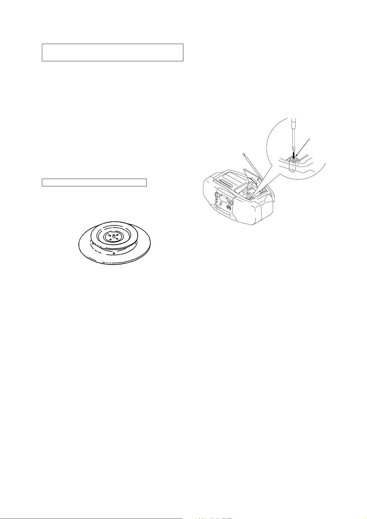
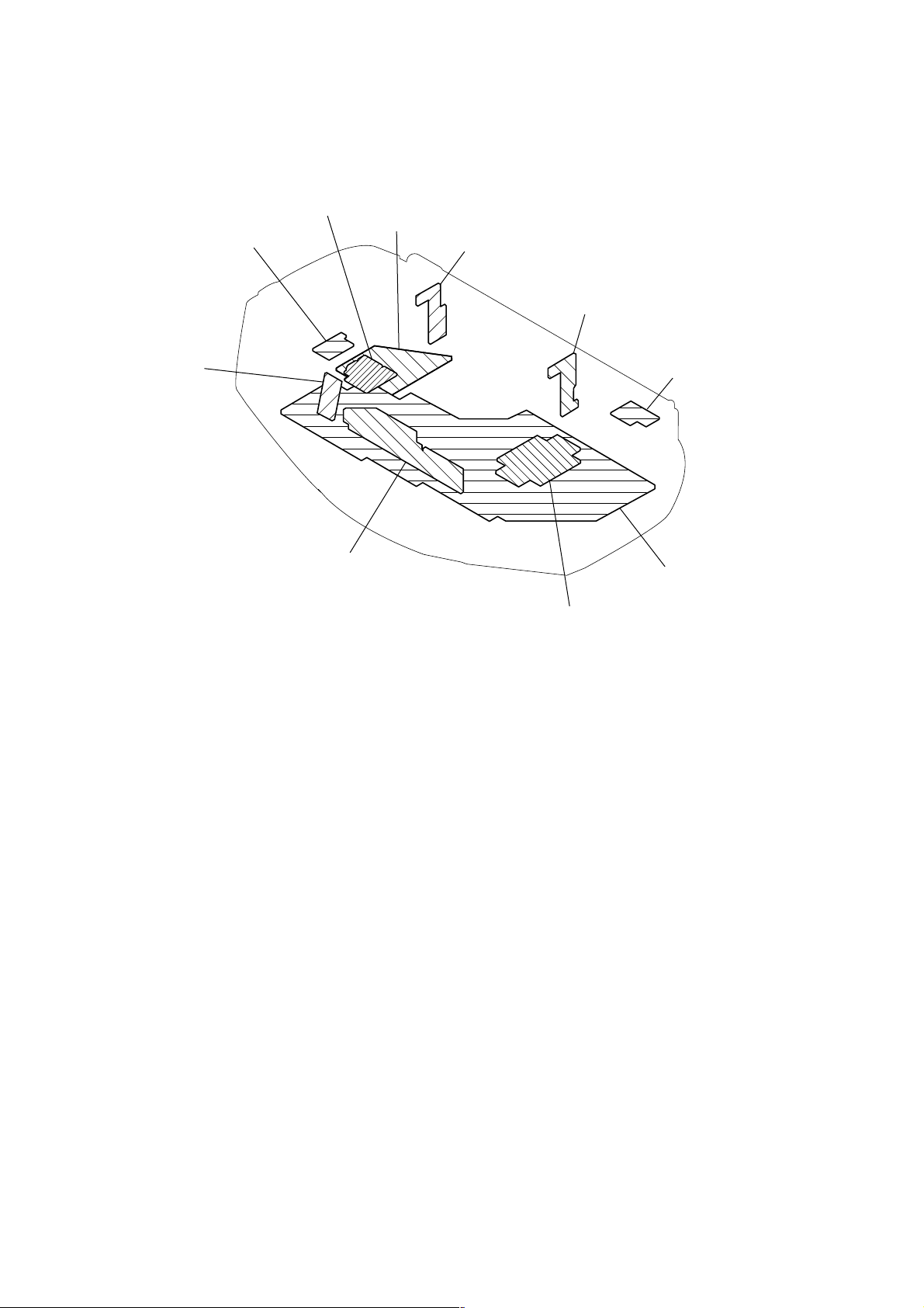
CHUCK PLATE JIG ON REPAIRING
On repairing CD section, playing a disc without the CD lid, use
Chuck Plate Jig.
• Code number of Chuck Plate Jig : X-4918-255-1
LASER DIODE AND FOCUS SEARCH OPERATION
CHECK
1. Press CD open knob.
2. Open the lid for CD.
3. Push on SWITCH (S801) as following figure.
4. Confirm the laser diode emission while observing the
objecting lens. When there is no emission, Auto Power
Control circuit or Optical Pick-up is broken.
Objective lens moves up and down once for the focus
search.
Insert a precision
screw driver and push
SWITCH (S801)
3
Page 4
CFD-V3/V7/V7L
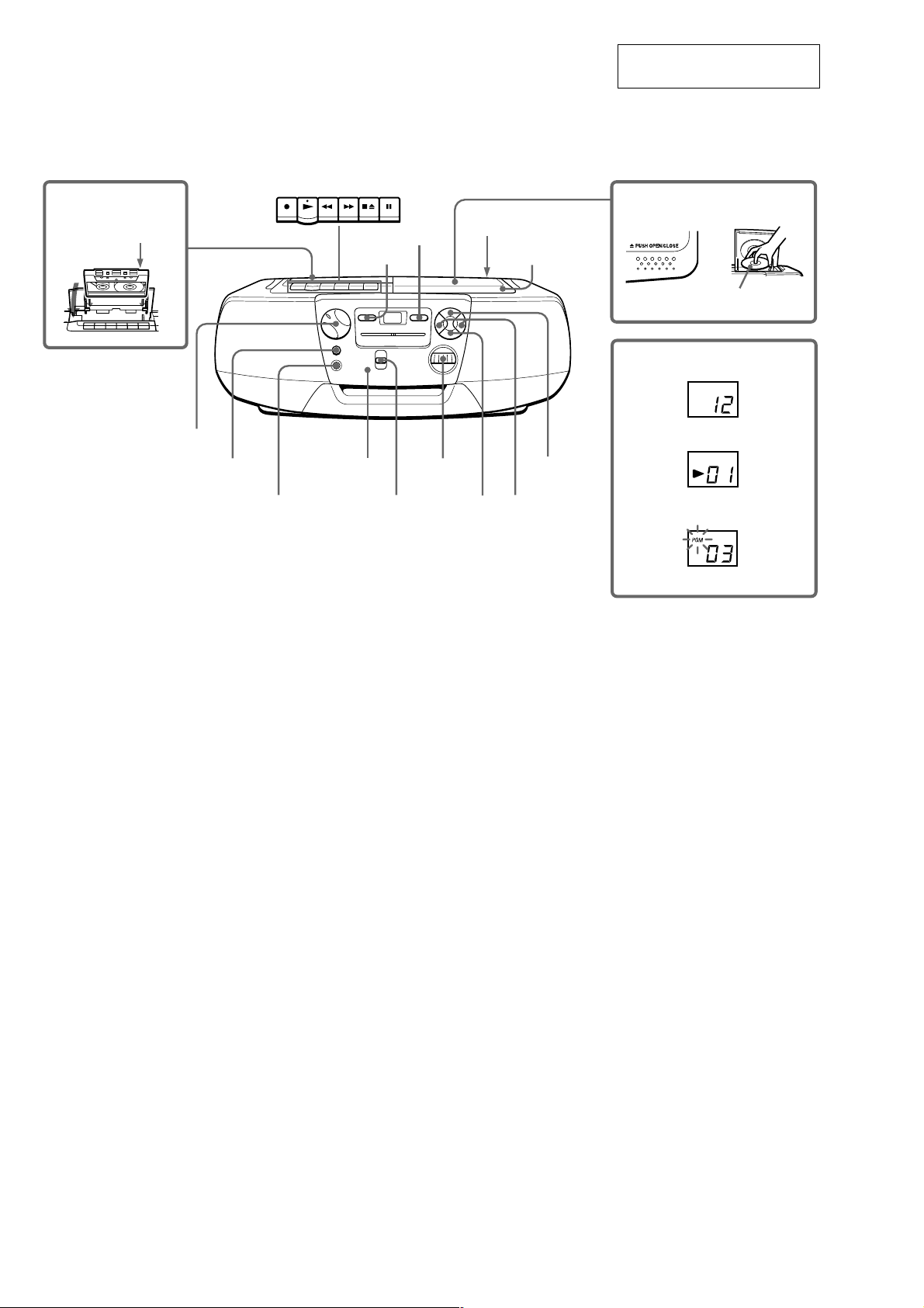
LOCATION AND FUNCTION OF CONTROLS
SECTION 2
GENERAL
This section is extracted from
instruction manual.
Inserting a cassette
With the side you want to
play facing upward
* FM MODE•ISS for CFD-V7L
VOLUME
MEGA BASS
REC PLAY REW FF
i
STOP/EJECT
PAUSE
PLAY MODE
ENTER
OPR/BATT
FUNCTION .,>
TUNING
FM MODE (rear)
Z PUSH OPEN/CLOSE
x
u
Loading a CD
c
With the labeled side up
Display
C
Total track number
D
Track number
E
Programmed track
4
Page 5
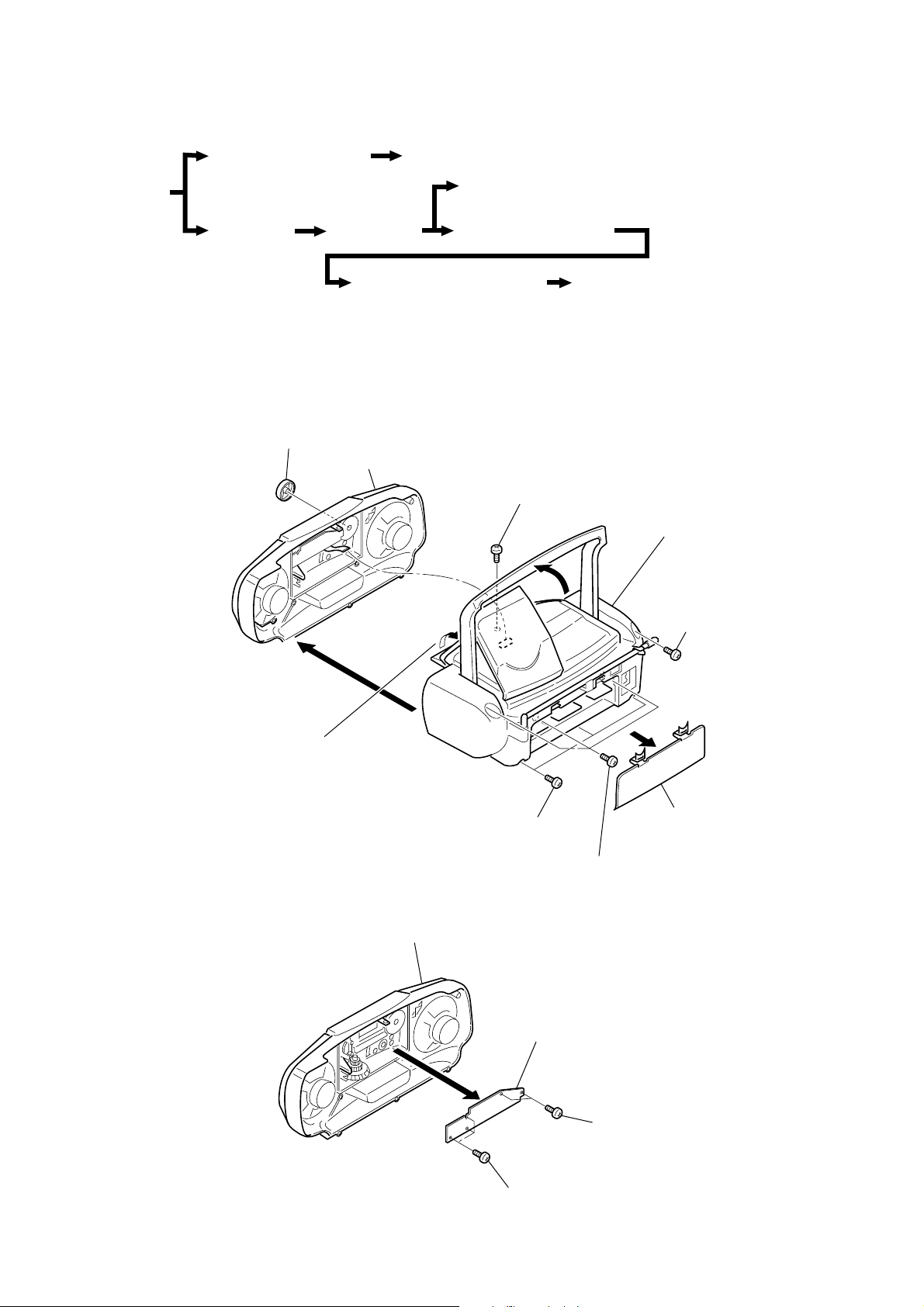
DISASSEMBLY
8
z
The equipment can be removed using the following procedure.
SECTION 3
CFD-V3/V7/V7L
Ver 1.1 2001.04
Cabinet (front) sub ASSY
Set
Cabinet (rear) Cabinet (upper)
Control board
Power board, Inlet board,
BATT (R) board, BATT (L) board
Volume board,
FM SW board, Main board
PRE board, Mechanism deck,
Optical pick-up section, CD board
Note : Follow the disassembly procedure in the numerical order given.
3-1. CABINET (FRONT) SUB ASSY, CABINET (REAR)
Knob (vol )
8
Cabinet (front) sub assy
7
Screw
+BVTP 3
5
Belt, M601 (capstan/reel motor),
HRP901 Head, Magnetic (Record/playback),
HE901 Head (Erase)
×
12
Cabinet (rear)
4
Screw
+BVTP 3
×
12
3-2. CONTROL BOARD
6
Open the Lid (CD)
9
Cabinet (front) sub assy
3
3
Screws
+BVTP 3
CONTROL board
×
12
2
Screws
+BVTP 3
1
Lid, battery case
×
12
2
Screws
+BVTP 2.6
1
Screws
+BVTP 2.6
×
8
×
5
Page 6
CFD-V3/V7/V7L
8
3-3. CABINET (UPPER)
5
6
Screw +BVTP 3 × 10
2
Open the Holder assy, cassette by
pressing STOP/EJECT button.
Screw +BVTP 3 × 12
STOP/EJECT
button
1
Screws
+BVTP 3
×
12
3
Open the Lid (CD)
Cabinet (upper)
4
Screw
+BVTP 3
Remove the handle in
the direction of the arrow.
×
12
8
9
7
CNP902
(POWER board)
3-4. POWER BOARD, INLET BOARD, BATT (R) BOARD, BATT (L) BOARD
BATT (R) board
4
CNP907
8
Cabinet (rear)
5
Screws
+WH 3
×
8
6
CNP90
1
+BVTP 3 × 10
6
Screws
POWER board
2
+BVTP 3 × 10
Screws
3
INLET board
CNP907
7
BATT (L) board
Cabinet (rear)
Page 7
3-5. VOLUME BOARD, FM SW BOARD, MAIN BOARD
)
4
Remove solder
(four places)
0
Screws
+BVTP 3 × 10
MAIN board
5
Screw
+BVTP 3
FM SW board
2
Remove solder
(five places)
CFD-V3/V7/V7L
Ver 1.1 2001.04
×
10
7
Wire, parallel (CN802)
(15 core)
6
KH801
1
Screws
+BVTP 3 × 10
qa
S801
3
VOLUME board
8
CNP304
9
Wire, parallel (CNP305)
(10 core) (V3, V7)
(12 core) (V7L)
Cabinet(upper)
3-6. PRE BOARD, MECHANISM DECK, OPTICAL PICK-UP SECTION, CD BOARD
8
7
Remove solder
(four places)
5
Screws
+PWH 2.6
×
10
CD board
9
Screw
+BVTT 2
×
6
0
Wire, parallel (CNP701
(16 core)
5
Screws +PWH 2.6 × 10
1
Screws +BVTP 3 × 10
3
Screw +BVTT 2 × 6
PRE board
Optical pick-up section
6
2
4
1
Screw
+BVTP 3
Mechanism deck
Cabinet(upper)
×
10
7
Page 8
CFD-V3/V7/V7L
)
Ver 1.1 2001.04
3-7. BELT, M601 (CAPSTAN / REEL MOTOR), “ HRP901 HEAD, MAGNETIC (RECORD/PLAYBACK) ”,
HE901 HEAD (ERASE)
HRP901 Head, Magnetic (Record/ Playback)
HE901 Head (Erase)
7 Claws
5 Claws
3-8. OPTICAL PICK-UP (KSS-213C)
8
3 Belt
1 Screws
+B 2.6 × 5
Mechanism deck
6
2
4 M601
(Capstan/reel motor)
Claws
4
Shaft, sled
Cover, CD
Claw
Optical pick-up (KSS-213C)
1
Claw
3
Bend the stopper
5
Gear
Claw
2
Chassis ASSY, motor (MB) (spindle
8
Page 9
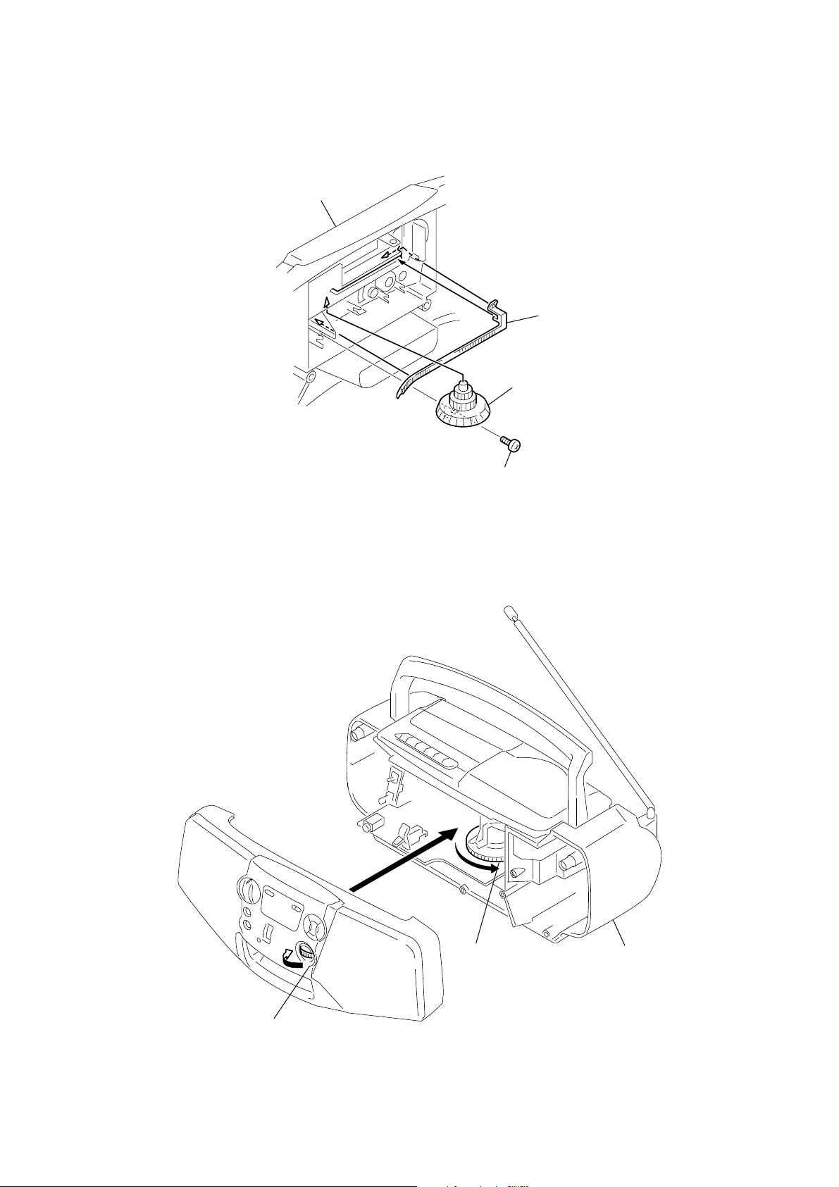
SECTION 4
)
DIAL POINTER INSTALLATION
Note : Follow the installation procedure in the numerical order given.
1 Align the pointer with the groove of “cabinet (front) sub ASSY” and insert it as shown in the illustration.
2 Align knob (TU) with “cabinet (front) sub ASSY” and fasten the screw.
Cabinet (front) sub ASSY
1 Pointer
knob (Tu)
CFD-V3/V7/V7L
2 Screw (+BVTP 2.6 × 8)
3 Turn the knob (TU) fully in the direction of the allow as shown in the illustration.
4 Turn the tuning capacitor gear fully in the direction of the allow as shown in the illustration.
5 Fasten the “cabinet (front) sub ASSY” and cabinet (rear) with the screws.
5
3
Tuning knob
4
Tuning capacitor gear
Cabinet (rear
9
Page 10
CFD-V3/V7/V7L
c
r
y
SECTION 5
ADJUSTMENTS
5-1. MECHANICAL ADJUSTMENTS
PRECAUTION
1. Clean the following parts with a denatured-alcohol-moistened
swab :
record/playback head pinch roller
erase head rubber belts
capstan
2. Demagnetize the record/playback head with a head demagnetizer. (Do not bring the head demagnetizer close to the erase
head.)
3. Do not use a magnetized screwdriver for the adjustments.
4. The adjustments should be performed with the rated power supply voltage (9V) unless otherwise noted.
Torque Measurement
Torque Torque Meter Meter Reading
1.77 – 5.88 mN•m
Forward CQ-102C (18 – 60 g•cm)
(0.25 – 0.83 oz•inch)
Forward
Back Tension
Fast Forward CQ-201B (45 – 95 g•cm)
Rewind CQ-201B (45 – 95 g•cm)
CQ-102C (1.0 – 5.0 g•cm)
Tape Tension Measurement
Torque Meter Meter Reading
CQ-403A
0.1 – 0.49 mN•m
(0.014 – 0.069 oz•inch)
4.42 – 9.31 mN•m
(0.62 – 1.32 oz•inch)
4.42 – 9.31 mN•m
(0.62 – 1.32 oz•inch)
more than 60g
(more than 2.12 oz)
Adjustment Location : Mechanism deck
Tape speed adjustment
control inside motor
TUNER SECTION
0dB = 1 µV
AM Section
Function switch : AM or LW
Volume : MIN
AM RF signal
generator
Put the lead-wire
antenna close to
the set.
5-2. ELECTRICAL ADJUSTMENTS
TAPE RECORDER SECTION
Standard Output Level
Output terminal HP OUT
load impedance 32 Ω
output signal level 0.25V (–10dB)
Test Tape
Type Signal Used for
WS-48A 3kHz, 0dB Tape Speed Adjustment
Tape Speed Adjustment
Procedure :
Mode : Playback
test tape
WS-48A
(3kHz, 0dB)
set
Adjustment Value : 3,000Hz
Standard Value : 2,940 - 3,060Hz
Frequency difference between the beginning and the end of the tape
should be within 1.5% (45Hz).
32Ω
J301 (phones)
0dB = 0.775V
digital frequenc
counter
30% amplitude modulation by 400Hz
signal.
Output level : as low as possible
FM Section
Function switch : FM
Volume : MIN
FM RF signal
generator
22.5kHz frequency deviation by
1kHz signal.
Output level : as low as possible
set
32Ω
J301 (phones)
0.01µF
level mete
telescopi
antenna
terminal
10
Page 11
• Repeat the procedures in each adjustment several times, and the
)
8
GND
51pin
TEST mode : momentarily short
[MAIN BOARD] (Conductor side)
R730
C
J
W
C
frequency coverage and tracking adjustments should be finally
done by the trimmer capacitors.
• Abbreviation
CET : East European & Russian
SP : Singapore
AM/LW IF ADJUSTMENT
Adjust for a maximum reading on level meter.
T2 455kHz
EXCEPT V7L
AM FREQUENCY COVERAGE ADJUSTMENT
Adjust for a maximum reading on level meter.
L4 520kHz ( 520kHz) < 516kHz>
CT4 1,780kHz (1,680kHz) <1,630kHz>
( ) : V3/V7: AEP, UK, CET, SP,KR
< > : V7:Italian
[ ] : V7L
C844
C8
C
IC801
R851
C801
CFD-V3/V7/V7L
R
R816
R815
R814
R813
R812
R811
C810
R810
21
JW316
S351
-1 -2
320
JC310
JW317
JW318
AM TRACKING ADJUSTMENT
Adjust for a maximum reading on level meter.
L3 620kHz
CT3 1,400kHz
V7L
LW FREQUENCY COVERAGE ADJUSTMENT
Adjust for a maximum reading on level meter.
L4 145kHz
CT4, CV2 300kHz
LW TRACKING ADJUSTMENT
Adjust for a maximum reading on level meter.
L3 160kHz
CT3, CV3 260kHz
FM IF ADJUSTMENT
Adjust for a maximum reading on level meter.
T1 10.7MHz
FM FREQUENCY COVERAGE ADJUSTMENT
Adjust for a maximum reading on level meter.
L2 86.5MHz ( 87.0MHz) < 87.35MHz> [ 87.0MHz]
CT2 109.5MHz (108.3MHz) <108.25MHz> [108.3MHz]
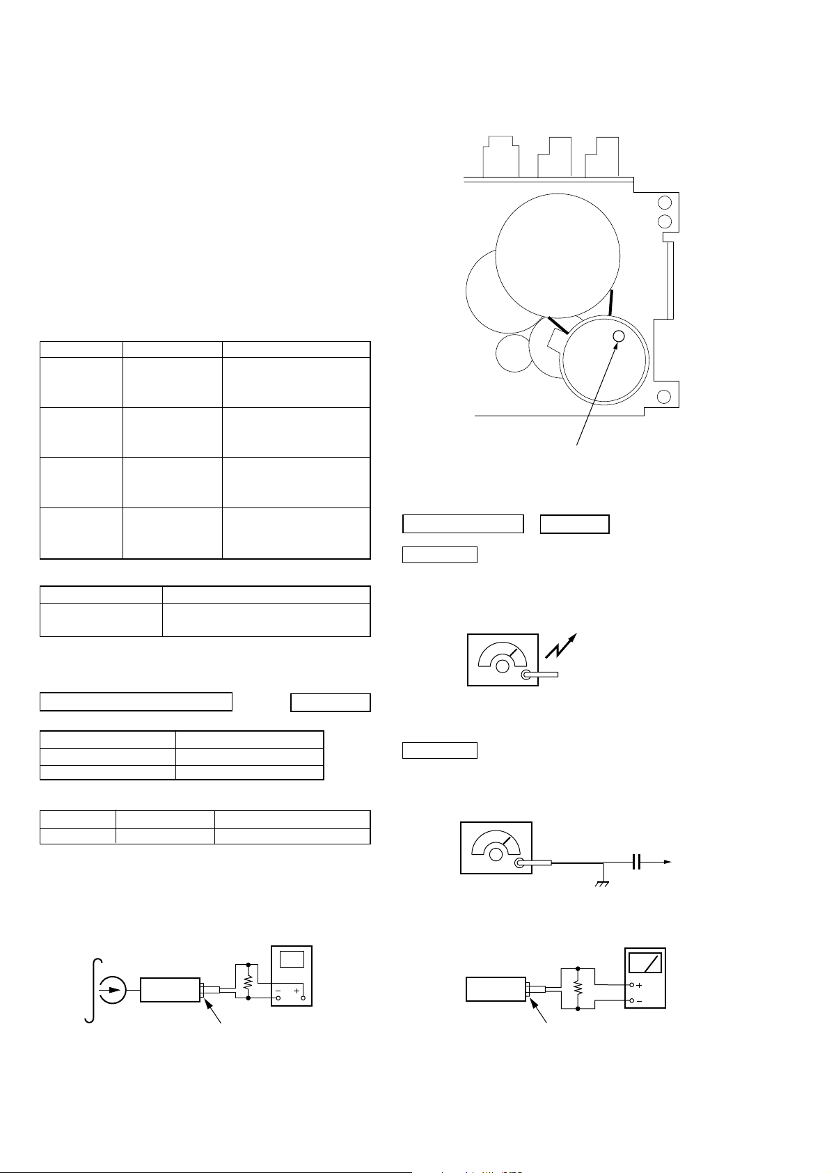
CD section adjustments are done automatically in this set.
In case of operation check, confirm that focus bias.
Focus Bias Check
1. Connect the oscilloscope between TP (RF) and GND on CD
board.
2. Insert the disc (YEDS-18). (Part No. : 3-702-101-01)
3. Press the 7 button two times (LPC ON).
4. Confirm that the oscilloscope waveform is as shown in the figure below. (eye pattern)
A good eye pattern means that the diamond shape (◊) in the
center of the waveform can be clearly distinguished.
• RF Signal Reference Waveform (eye pattern)
VOLT/TV : 200mV
TIME/DIV : 500 nS
RF level
0.7 – 1.0 Vp-p (LPC ON)
1.0 – 1.4 Vp-p (LPC OFF
When observing the eye pattern, set the oscilloscope for AC range
and raise certical sensitivity
oscilloscope
(AC range)
L1 86.5MHz ( 87.0MHz) < 87.35MHz> [ 87.0MHz]
CT1 109.5MHz (108.3MHz) <108.25MHz> [108.3MHz]
Adjustment Location : Main board (See page 12)
CD SECTION
How to put the set into CD Test Mode
1. Set the function switch to power off.
2. Set the function switch to CD.
3. Set Test mode by momentarily shorting both of the IC801 51pin
to GND. (Shorting the terminals momentarily is sufficient).
The set is into CD test mode (88 is displayed).
4. Turn the power off to release test mode.
FM TRACKING ADJUSTMENT
Adjust for a maximum reading on level meter.
[CD BOARD] (Conductor side)
JW710
R701
R706
R709
R705
R703
R702
R710
R704
C736
703
R711
C705
(RF)
TP
TP (RF)
R708
C734
2
(GND)
C731
C704
JW726
IC701
J
C703
C743
C730
R729
C747
C744
11
Page 12
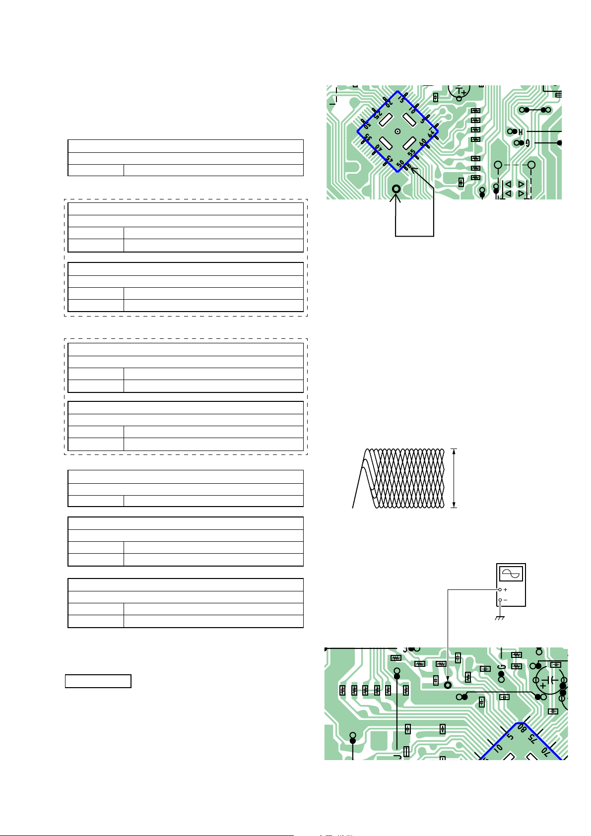
CFD-V3/V7/V7L
Adjustment Location :
[MAIN BOARD]
(Component side)
L4 : AM/LW Frequency
Coverage Adjustment
L3: AM/LW Tracking Adjustment
T1 : FM IF Adjustment
T2 : AM/LW IF Adjustment
CV2 : LW Frequency Coverage Adjustment
(V7L)
L2 : FM Frequency Coverage Adjustment
L1 : FM Tracking Adjustment
CV3: LW Tracking Adjustment (V7L)
[MAIN BOARD]
(Conductor side)
CT1 : FM Tracking Adjustment
CT3 : AM/LW Tracking Adjustment
CT2 : FM Frequency
Coverage Adjustment
CT4: AM/LW Frequency
Coverage Adjustment
12
Page 13
CFD-V3/V7/V7L
SECTION 6
DIAGRAMS
6-1. EXPLANATION OF IC TERMINALS
IC801 µPD789316GK-903 SIGNAL PROCESSOR, D/A CONVERTER, LCD DRIVE, SYSTEM CONTROL
Pin No. Pin name I/O Description
1 – 4 NC — Not used (open)
5 IC — Connect to ground.
6 XT1 I Connect to ground.
7 XT2 — Not used (open)
8 VDD — Power supply terminal (B+ 3.3 V)
9 VSS — Ground terminal
10 CL1 I Oscillator terminal (4 MHz)
11 CL2 — Oscillator terminal (4 MHz)
12 RESET I Reset signal input
13 NC — Not used (open)
14 SYNC–R — Not used (open)
15 CE O Chip enable signal output
16 C–RST O Reset signal output to the LC78645E (IC701)
17 CAPH — Charge pump capacitor terminal
18 CAPL — Charge pump capacitor terminal
19 – 21 VLC0 – 2 — Capacitor connect terminal
22 – 25 COM0 – 3 O LCD common drive output
26 – 43 S0 – 17 — Not used (open)
44 – 48 S18 – 22 O LCD segment drive output
49 S23 — Not used (open)
50 ENTER I Key (ENTER) input
51 MODE I Key (MODE) input
52 PLAY I Key (H PLAY) input
53 FR I Key (l FR) input
54 FF I Key (L FF) input
55 STOP I Key (s STOP) input
56 DOOR I Door open/close input
57 WRQ I Command signal input
58 TEST I Test mode signal terminal input (TEST: L)
59 MUTE O Mute signal output
60 FSEQ I Frame SYNC signal input
61 DRF I DRF (Defect RF) input
62 DO O Serial data output
63 DIN I Serial data input
64 CLK I Clock signal input
13
Page 14
CFD-V3/V7/V7L
d
• Circuit Boards Location
VOLUME board
POWER board
PRE board
INLET board
BATT (R) board
BATT (L) board
FM SW boar
CONTROL board
MAIN board
CD board
14
Page 15
6-2. BLOCK DIAGRAMS –TUNER/TC SECTION–
ANT1
TELESCOPIC ANTENNA
V7L
FM
CV3,CT3,L3
LW
TRACKING
CV2,L4,CT4
LW FREQUENCY
COVERAGE
EXCEPT V7L
TRACKING
AM FREQUENCY
COVERAGE
CT3,L3
L4,CT4
D1
AM
D2
FM FREQUENCY
FERRITE-ROD
CT1,L1
TRACKING
CT2,L2
COVERAGE
L3
AM/LW
ANTENNA
FM
L4
AM
OSC
L1
FM
RF
L2
FM
OSC
V7L
CV3
CV2
CT3
CT4
CT1
CT2
CV1-1
CV1-2
CV1-3
CV1-4
TU +6V
FM/AM
FRONT-END
IF AMP,DET,FM MPX
IC1
RF
IN
FRONT-END
FM RF OUT
FM OSC
AM RF
IN
FRONT-END
AM OSC
FM
AM
MIX
OUT
T2
AM IF
CF2
TU +6V
CF1
TU +6V
T1
FM IF
FM
IF IN
AM
IF IN
-11
-12
FM DET
AM DET
TU +6V
QUAD
DET OUT
V7L
CFD-V3/V7/V7L
Ver 1.5
LPF1
L OUT
R OUT
TU +6V
R-CH
S1
EXCEPT V7L
FM MODE
MONO
STEREO
FM MODE
ISS
MONO
1
STEREO
2
V7L
MPX IN
Q2
MPX
LPF2
Q1
CD
SECTION
CD L-CH
CD R-CH
HRP901
RECORD/
PLAYBACK
HEAD
HE901
ERASE
HEAD
R-CH
TU IN L
CD IN L
PRE/REC
AMP
IC301
MUTE
REG
6
BUFFER
REF
T301
-2
-1
L.LINE
22
L.RAD
24
MIC AMP
MIC
13
MUTE
PB AMP
L.IN
5
L.RO
4
PB AMP
REC
AMP(26dB)
DET
TAPE
ALC
1
S301
REC
PB
21
TU +6V
REC
MONITOR
LOGIC
AMP
(7dB)
BIAS
OSC
Q301
L.LO
LINE
TAPE
20
17
15
V7L
ISS1
Q303
V7L
ISS
L.OUT
CD
TAPE
L.OUT
FM
CD
TAPE
MAIN
SECTION
MAIN
SECTION
• R-CH is omitted:
same as L-CH
• Signal path.
F : FM
f : AM
E : PLA Y
a : REC
J : CD
• IC link button.
-11
Last digit : -11
-12
Last digit : -12
1515
Page 16

CFD-V3/V7/V7L
Ver 1.5
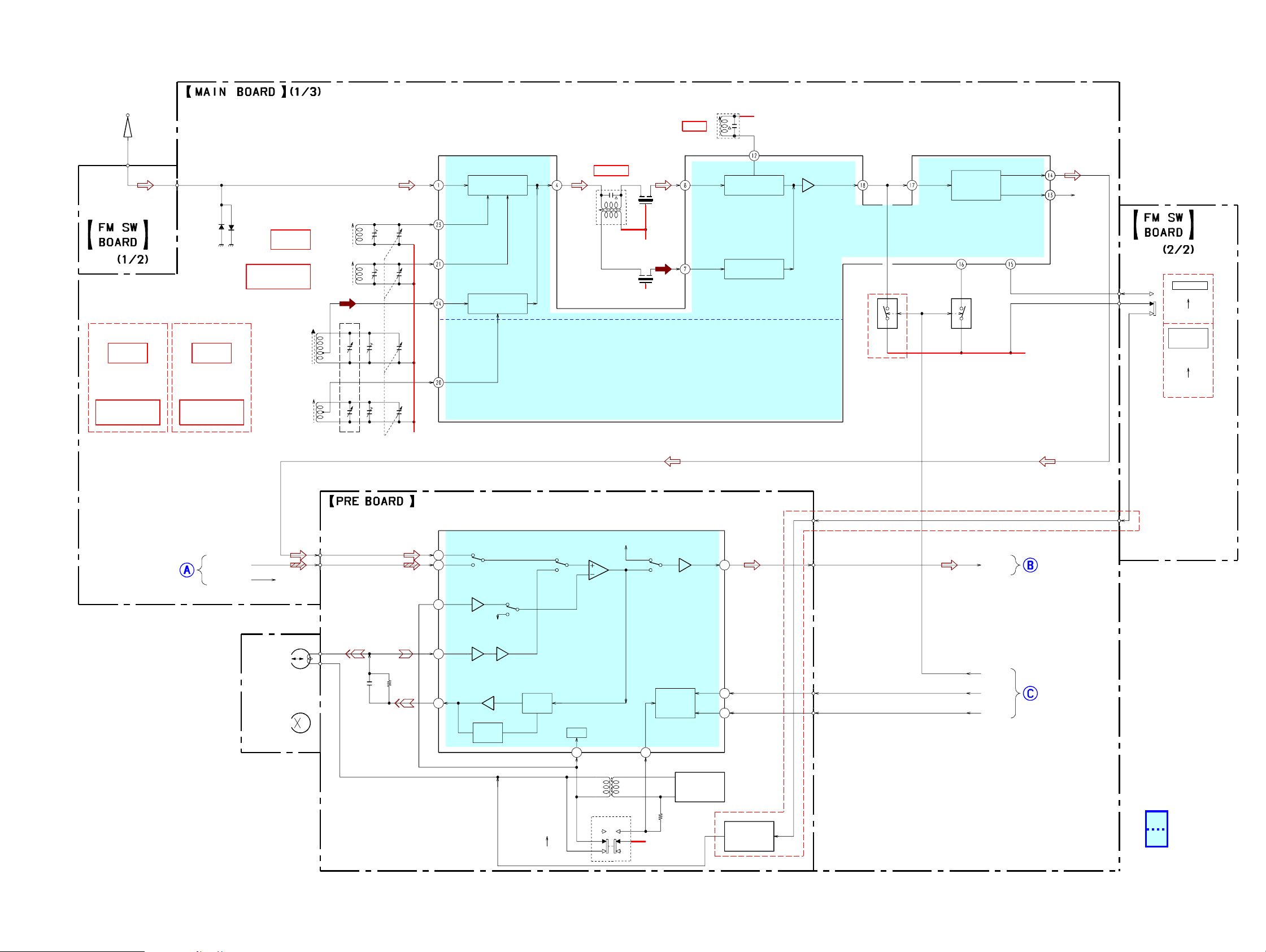
6-3. BLOCK DIAGRAMS –MAIN SECTION–
CD
SECTION
TUNER/TC
SECTION
RESET
L.OUT
MEGA BASS
ON
OFF
S355
RESET
Q801
RV352
VOLUME
CD +3.3V
D302
MUTE
Q101
R-CH
POWER
AMP
IC304
STANDBY
SWITCH
-11
-12
R-CH
J301
SP101
SPEAKER
(L-CH)
SP201
SPEAKER
(R-CH)
S801
CD DOOR
(OPEN/CLOSE)
DOOR
TUNER/TC
SECTION
TU +6V
TAPE +6V
CD+ 3.3V
CD +6V
RESET
DIGITAL SIGNAL
PROCESSOR,
LCD DRIVE,
SYSTEM CONTROL
IC801(1/2)
TAPE
POWER
SWITCH
Q311,312
POWER AMP
B+
(+8.9V)
D314
+6.9V REG
Q309,
Q311
POWER
SWITCH
Q402,Q405
E4
VOL SEL BOARD
S901
VOLTAGE
SELECTOR
220-240V AC
R
110-120V AC
CNJ901
AC IN
-1
-2
VOLTAGE
-11
DET
IC401
-12
FUNCTION
9V
AC
4.5V
S351-1
EXCEPT V7L
AM
LW
V7L
FM
CD
D901-904
F901
T901
POWER
TRANSFORMER
F901
EXCEPT E4
D309
FM
D303
D304
CD
+3.3V REG
Q310,
D308
(4MHz)
CL1
CL2
22
COM0
_
COM3
_
25
COM0-3
LCD401
LIQUID
CRYSTAL
DISPLAY
_
S22
_
48
S0-S4
ENTER
S18
44
S406
ENTER
MODE
S405
PLAY MODE
S404
CD CONTROL
PLAY
S403
FR
S402
STOP
FF
INITIAL
SWITCH
Q401
S401
D310
OPR/BATT
Q409
MOTOR
SWITCH
S601
(MD POWER)
CAPSTAN/REEL
MOTOR
M601
DRY BATTERY
SIZE "D"
(IEC DESIGNATION R20)
6PCS,9V
• R-CH is omitted: same as L-CH
• Signal path.
F : FM
• IC link button
-11
Last digit : -11
-12
Last digit : -12
1616
Page 17

6-4. BLOCK DIAGRAMS –CD SECTION–
CFD-V3/V7/V7L
Ver 1.5
OPTICAL PICK-UP
BLOCK
(KSS-213C)
LD
PD
REF
LD
PD
VR
CD RF/
SYSTEM SERVO
PROCESSOR
IC701
VC
A
B
C
D
E
F
LASER
POWER
CONTROL
G
Q701
VC
FIN1
FIN2
TIN1
TIN2
LDD
VREF
LDS
APC
TE
FE
SERVO
CONTROL
FDO
TDO
SPDO
RF
SLDO
PURPOSE
CONT5
CONT4
PORT
CONT2
CONT1
+
-
+
CONT3
EFMIN
XIN
DIGITAL
FILTER/
ERROR
CORRECTION
XOUT
D/A
COMMAND
INTERFACE
LCHO
RCHO
DRF
RES
WRQ
FSEQ
DO
DI
CL
CE
CD L-CH
CD R-CH
TUNER/TC
SECTION
TRACKING
COIL
FOCUS
COIL
M702
SLED
MOTOR
M701
SPINDLE
MOTOR
S701
(LIMIT)
SLED/SPINDLE MOTOR DRIVE,
TRACKING/FOCUS COIL DRIVE
IC702
T+
T-
F+
F-
+
-
+
-
SL+
SL-
SP+
SP-
VREF
LEVEL
LEVEL
LEVEL
LEVEL
SHIFT
SHIFT
SHIFT
SHIFT
MUTE
DRIVER
TIN
FIN
MUTE
SLIN
SPIN
RST
X701
33.86MHz
CE
DO
DIN
CLK
FSEQ
DIGITAL SIGNAL
PROCESSOR,
LCD DRIVE,
SYSTEM CONTROL
WRQ
IC801(2/2)
C-RST
-11
-12
DRF
RESET
• Signal path.
MAIN
SECTION
J : CD
• IC link button
SW
-11
Last digit : -11
-12
Last digit : -12
1717
Page 18

CFD-V3/V7/V7L
Ver 1.2 2001.08
6-5. PRINTED WIRING BOARDS – MAIN SECTION – (Last digit : -11) z Refer to page 14 for Circuit Boards Location.
1
MAIN
A
BOARD
2 3 4 5 6 7 8 9
S801
CD DOOR
(OPEN/CLOSE)
A
CD BOARD
CNP702
z
Semiconductor
Ref. No. Location
KH2
JC1
C891
C30
C2
JC2
JC4
JC6
R2
JW335
JW334
CF1
C4
R30
R8
C19
C10
V3/V7:AEP,
CET,UK,SP,IT/
V7L
CF2
C14
C13
C8
R4
C17
12
10
5
JW332
1
C15
JW333
C1
V7L
C3
Q2
V3/V7
C24
R1
IC1
C18
C25
R9
C26
C22
C23
C9
CN802
Q1
C27
C20
13
15
20
C11
R3
24
C12
JC5
V3/V7:AEP,
CET,UK,SP,IT/
V7L
JW331
FERRITE-ROD
V3/V7:AEP,
CET,UK,SP,IT/
V7L
CV-1
C21
L2
CT2
CT1
C32
R20
L3
AM/LW
ANTENNA
CV2
CV1-2
CV1-1
C5
L1
R11
CV1-4
CV1-3
C6
S801
D2
D1
KH801
B
T1
T2
C
D
ANT1
FM
TELESCOPIC ANTENNA
FM SW BOARD
E
KH1
S1
11
1-680-678-
F
FM MODE
STEREO
S1
t
MONO
(11)
V3/V7
FM MODE
ISS
t
MONO
V7L
STEREO
1 2
VOLUME BOARD
KH307
RV352
RV352
VOLUME
R123
C124
R223
R124
C224
R224
C223
JW330
V7L
CT4
CT3
JW328
D303
C123
C171
JW329
V3/V7
C7
JC7
L4
C36
R315
R314
D304
D314
S355
1-680-679-
S355
MEGA BASS
r
OFF
T
R
ON
V7L
C28
C31
JW327
D309
R319
C271
C29
11
(11)
C314
C317
CV3
C346
JW326
JW325
R806
Q801
C842
C843
C844
IC801
CONTROL BOARD
Q310
C841
CN401
D308
JW324
R819
CN801
B
C345
Q311
R818
R851
C348
C805
R805
R360
C851
1
2
CNP305
R349
R355
R354
ICP301
JW315
C802
R816
C801
R815
R814
R813
R812
R811
R810
C810
R809
JW321
D302
TAPE CD/RADIO OFF
V3/V7
TC BOARD
CN303
D
5
JC306
R353
R352
R351
R801
S351
-1 -2
JW320
JW323
S351
FUNCTION
AM
FM
CD
9
JW312
Q312
JW313
Q309
JW316
R344
LW
11
JC310
JW317
JW318
R340
R341
12
JW314
JW319
JW322
V7L
V7L
JW311
C347
C156
C351
R386
R342
D310
OPR/BATT
JW310
C256
C252
C152
R343
R253
Q101
Q201
C320
JW309
C349
JW308
JW307
C343
D311
R251
R151
4
R153
IC304
KH306
C341
CNP304
C255
C155
C253
C153
C154
1
JW306
R346
R345
JW305
JW304
1
C316
Q409
KH902
JW303
C401
C254
4
3
2
1
4
IC401
R154
R401
R403
Q402
S601
(MD POWER)
+
M601
CAPSTAN/REEL
MOTOR
-
INLET BOARD
C
CNP902
D306
JC303
R414
R415
C402
JC302
R416
R413
B
C
E
Q401
JC401
R417
CNP303
JW301
JC305
SP101
SPEAKER
(L-CH)
SP201
R418
D301
JW302
R404
R401
R402
E
C
B
Q405
M
SPEAKER
(R-CH)
R254
1-680-676-
11
(11)
J301
i
Note:
• X : parts extracted from the component side.
• : Pattern from the side which enables seeing.
• Abbreviation
D1 A-1
D2 A-1
D301 D-8
D302 E-6
D303 D-4
D304 D-4
D306 D-9
D308 C-5
D309 D-4
D310 E-7
D311 D-7
D314 E-4
IC1 C-3
IC304 E-7
IC401 D-8
IC801 D-5
Q1 B-3
Q2 C-3
Q101 E-7
Q201 E-7
Q309 D-7
Q310 C-5
Q311 C-6
Q312 C-6
Q401 E-9
Q402 E-8
Q405 E-8
Q409 C-8
Q801 D-5
CND : Canadian
IT : Italian
CET : East European & Russian
SP : Singapore
AR : Argentina
AUS : Australian
TW : Taiwan
KR : Korean
1818
Page 19

6-6. SCHEMATIC DIAGRAMS – MAIN SECTION (1/3) – ( Last digit : -11) z Refer to page 30 for Notes. z Refer to page 31 for IC Block
V3/
V7:AEP,CET,
UK,IT/
V7L
CV1-3
CT3
V7L
C36
10p
CV3
50p
L3
AM/LW
FERRITE-ROD
ANTENNA
C32
4.7p
CT1
R3
3.3k
L1
C11
10p
C12
10p
CV1-2
CT2
L2
CV1-1
C5
C6
5p
10p
C7
*
V7L
CV2
30p
CV1-4
CT4
V7L
C28
470p
JC7
C29
100p
C31
470p
V3/V7
CFD-V3/V7/V7L
V3/V7
L4
V7L
D1
1SS133T-77
V3/V7
*
C7
C19
C20
R20
V3:AR/
V7:CND,AR
AUS,TW
2.2PF
0.022uF
0.022uF
1k
D2
1SS355T-77
V7L
V3:AEP,CET,SP/
V7:AEP,
CET,UK,SP
4.7PF
0.01uF
0.01uF
1k
R1
220
V7:IT
4.7PF
0.01uF
0.01uF
1k
R20
*
C1
1000p
C23
10
50V
V7L
0.01uF
0.01uF
100
C20
V7L
Q2
KRA302-RTK
SWITCH
C26
4700p
KH2
JC2
JC1
4
1
0
0
ISS1
TU +B
JC4
100
C8
4.7
50V
C9
4.7
50V
R11
R30
220
10k
*
4.7p
C21
JC5
0
IN
RF
VCC
-
FM/AM/LW
FRONT-END,IF AMP,
DET,FM MPX
T2
330
R2
C24
0.01
JC6
0
AM RF
FM-RF
IN
FM RF
C13
0.47
OUT
RF
AM LOW
GND
FM OSC
CUT
MIX
C14
4.7
AM OSC
OUT
AFC
IC1
TA2111N
AGC
VCC
DET
AM IF
CF1
OUT
IN
MPX
FM IF
IN
C22
IN
1
CF2
LPF2
0.01
GND
C3
C25
100p
V3/V7
LPF1
TUN
LED
C30
2p
L-OUT
LED
ST
C4
22
C15
0.1
R-OUT
QUAD
C2
10p
T1
C17
0.1
V3:AEP,CET,SP/
V7:AEP,CET,
UK,SP,IT/
V7L
C10
4700p
R4
3.3k
C18
1
C27
4700p
R8
22k
Q1
KRA302-RTK
SWITCH
R9
22k
C19
*
TU.L
TU.R
FM
TU.GND
S-GND
ANT1
FM
TELESCOPIC
ANTENNA
KH1
4
1
S1
FM MODE
MONO
STEREO
FM MODE
ISS
MONO
1
STEREO
2
1919
Page 20

CFD-V3/V7/V7L
Ver 1.1 2001.04
6-7. SCHEMATIC DIAGRAMS – MAIN SECTION (2/3) – ( Last digit : -11)
S355
MEGA BASS
1k
S351-1
FUNCTION
AM
LW
D304
1SS355TE-17
R314
4.7k
C348
KTZ 3.9-RTK
100
10V
ON
OFF
V3/V7
V7L
D314
D308
FM
1SS355TE-17
C317
22
25V
C346
0.01
TU_IN_L
TU_IN_R
CD_IN_L
CD_IN_R
L_OUT
R_OUT
TAPE
SYNC-R
V7L
TU.L
TU.GND
TU.R
TU +B
S-GND
CD
6V
GND
ISS1
ISS1
FM
CNP305
12P
JC306
0
C171
10
50V
C271
10
50V
R124
6.8k
C123
0.47
50V
TAPE CD RADIO OFF
JC310
0
D309
1SS355TE-17
C314
47
10V
R315
R319
1k
4.7k
KTC3203Y-AT
+3.3V REG
C124
4700p
R123
D303
1SS355TE-17
Q310
R349
330
z
Refer to page 30 for Notes.
C224
4700p
KH307
CD
C345
0.01
R224
6.8k
C223
0.47
50V
R223
1k
5
5P
5
D302
1SS355TE-17
KTB1241Y-AT
1k
R351
Q311,312
+B SWITCH
Q311
1k
R352
ICP301
R360
100k
1k
1k
R353
R354
Q312
KRC405
RTK
RV352(1/2)
20kB
1
1
KH306
5P
R151
4.7k
R251
4.7k
1k
R355
C347
220
10V
KRC410-RTK
C316
1
50V
z
Refer to page 33 for IC Block Diagram.
RV352
VOLUME
RV352(2/2)
20kB
Q101
JC305
0
Q309
2SD2396K
+6.9V REG
D311
KDZ 7.5-RTK
1SS355TE-17
JC401
1k
R345
C343
0.01
D301
0
1k
R346
Q201
KRC410-RTK
Q101,201
KTA1266-GR
R413
4.7k
R416
4.7k
C402
50V
MUTE
Q401
INITIAL
SWITCH
10
R414
6.8k
R415
6.8k
R253
470
KTA1266-GR-AT
Q402
KRC402
Q402,405
POWER SWITCH
Q409
KTC3203Y-AT
MOTOR
SWITCH
C252
C152
1000p
C256
47
10V
TAPE CD RADIO OFF
C320
0.022
Q405
R417
10k
R418
10k
D306
1SS355TE-17
1000p
4
C156
47
10V
470
R153
C351
47
10V
S351-2
FUNCTION
AM
LW
R386
3.3k
CNP304
1
V3/V7
V7L
R343
D310
L-34HD
OPR/BATT
4P
C153
FM
3.3k
47
10V
C154
470
10V
C155
0.1
CD
R344
220
3.3k
R342
C341
3300
16V
C254
470
10V
C255
0.1
3.3k
R341
3.3k
R340
C253
47
10V
R402
10k
R403
22k
IC304
BA5417
POWER AMP
R254
R154
MM1468XD
VOLTAGE
VCC
TC
N.C.
VOUT
C401
100
10V
100
100
IC401
DETECT
CONT
N.C.
VM
GND
C349
10000p
JC302
JC303
0
CNP303
4P
4
1
KH902
4P
1
GND
9V
AC
4.5V
4
0
R404
1k
R401
100k
+
-
+
-
J301
SP201
SPEAKER
(R-CH)
SP101
SPEAKER
(L-CH)
P.GND
R-OUT
L-OUT
TU-GND
UCOM-GND
TU +B
CD 6V
D.GND
CD 3.3V
AU MUTE
M601
CAPSTAN/REEL
S601
(MD POWER)
MOTOR
2020
Page 21

CFD-V3/V7/V7L
6-8. SCHEMATIC DIAGRAMS – MAIN SECTION (3/3) – ( Last digit : -11)
CN802
15P
P.GND
CD6V
FSEQ
DRF
DO
*WRQ
CL
CE
*RES
R-CH
L-CH
D.GND
CD3.3V
U-RESET
1
5
DI
10
15
R801
R805
220k
22
z
Refer to page 30 for Notes.
C851
22p
C802
10V
R818
100
R819
100
47
R851
4.7k
C801
0.1
z
Refer to page 13 for Explanation of IC Terminals.
C810
NC
NC
NC
NC
IC
XT1
XT2
VDD
VSS
CL1
CL2
RESET
NC
SYNC-R
CE
C-RST
100p
CLK
CAPH
DIN
CAPL
DO
VLC0
DRF
FSEQ
MUTE
DIGITAL SIGNAL
PROCESSOR
LCD DRIVER
SYSTEM CONTROL
COM0
VLC2
VLC1
TEST
COM1
WRQ
IC801
COM2
DOOR
COM3
STOP
S0
FF
S1
R810
R812
R813
R814
R815
R816
100
1k
1k
1k
100
100
R811
10k
R809
1k
16
10
FR
PLAY
S3
S2
MODE
S4
ENTER
S5
S23
S6
S22
S21
S20
S19
S18
S17
S16
S15
S14
S13
S12
S11
S10
CN801
16P
S9
S8
S7
STOP
FF
FR
PLAY/PAUSE
PLAY MODE
ENTER
GND
COM0
COM1
COM2
COM3
5
S0
S1
S2
S3
S4
1
S801
CD DOOR
(OPEN/CLOSE)
UCOM-GND
TU-GND
TU +B
R-OUT
L-OUT
D.GND
CD 3.3V
P.GND
CD 6V
AU MUTE
KH801
2P
C805
0.1
C842
0.1
C843
0.1
1
C891
2
1000p
R806
220
Q801
KRC404-RTK
RESET
C841
0.1
C844
0.1
2121
Page 22

CFD-V3/V7/V7L
Ver 1.4 2003.06
6-9. PRINTED WIRING BOARDS – MAIN SECTION – (Last digit : -12) (Added V7: E4, KR model) z Refer to page 14 for Circuit Boards Location.
1
MAIN
A
BOARD
2 3 4 5 6 7 8 9
S801
CD DOOR
(OPEN/CLOSE)
A
CD BOARD
CNP702
z
Semiconductor
Ref. No. Location
KH2
C891
JC2
R5
JW335
JW334
C30
C2
V3:AEP,CET,SP/V7:AEP,
CET,UK,SP,IT,KR/V7L
JC6
R2
R30
CF1
C4
C14
C13
C8
R8
R4
C17
C15
C19
C18
C9
CN802
JW331
Q1
L3
C10
CF2
12
10
5
1
JW332
JW333
Q2
V7L
C3
C24
R1
C1
IC1
R9
C27
V3:AEP,CET,SP/V7:AEP,
C20
CET,UK,SP,IT,KR/V7L
13
15
C26
C22
C25
20
V7L
EXCEPT
24
JC5
V3:AEP,CET,SP/
V7:AEP,CET,UK,
SP,IT,KR/V7L
C23
C21
L2
C11
R3
C12
C32
AM/LW
FERRITE-ROD
ANTENNA
CV2
CV-1
CV1-2
CT2
CT1
CV1-1
C5
L1
R20
R11
V7L
CV1-4
CV1-3
C6
S801
D2
D1
KH801
B
T1
T2
C
D
ANT1
FM
TELESCOPIC ANTENNA
FM SW BOARD
E
KH1
S1
12
EXCEPT
V7L
(12)
1-680-678-
F
FM MODE
STEREO
S1
t
MONO
FM MODE
ISS
t
MONO
V7L
STEREO
1 2
VOLUME BOARD
KH307
RV352
RV352
VOLUME
R123
C124
R223
R124
C224
R224
C223
JW330
CT4
CT3
JW328
D303
C123
C171
JW329
EXCEPT
V7L
C7
JC7
L4
C36
R315
R314
D304
D314
S355
1-680-679-
S355
MEGA BASS
r
OFF
T
R
ON
V7L
C28
C31
D309
JW327
R319
C271
C29
12
(12)
C346
CV3
C314
C317
CONTROL BOARD
(EXCEPT V7:E4)
CONTROL BOARD
JW326
Q801
C844
CN401
CN401
(V7:E4)
C843
JW325
R806
C842
D305
Q310
C841
IC801
D308
JW324
R819
CN801
B
B
C345
Q311
R818
R851
C348
C805
R805
1
C801
R349
C802
R816
R815
R814
R813
R812
R811
C810
R809
2
R354
R810
R360
C851
TAPE•CD/RADIO OFF
EXCEPT
V7L
CNP305
Q312
JW315
R801
JW321
D302
FUNCTION
D
(EXCEPT V7:E4)
D
5
JC306
EXCEPT IT
R348
JW313
R353
R352
R351
S351
-1 -2
JW320
JW323
S351
AM
FM
CD
TC BOARD
CN303
TC BOARD
CN303
(V7:E4)
11
12
9
R350
JW314
Q309
JC310
JW316
JW317
JW318
JW319
JW322
R344
R340
R341
V7L
LW
V7L
JW311
JW312
C347
C156
C351
IT
R386
R342
D310
OPR/BATT
JW310
C256
C252
C152
R343
Q101
Q201
JW309
JW308
R253
C320
C349
JW307
R251
R151
4
R153
IC304
KH306
C341
C343
D311
C255
C155
1
CNP304
JW306
EXCEPT IT
R346
R345
JW305
JW304
C153
C154
C253
1
C316
Q409
KH902
JW303
C401
C254
4
3
2
1
4
R154
R401
R403
IC401
Q402
R418
S601
(MD POWER)
+
M601
CAPSTAN/REEL
M
MOTOR
INLET BOARD
C
CNP902
(EXCEPT V7:E4)
INLET BOARD
C
CNP902
(V7:E4)
D301
JW302
R404
R401
R402
E
C
B
Q405
JC303
JC302
R416
JC401
R417
JW301
C402
B
C
E
CNP303
D306
R415
R413
Q401
JC305
SP101
SPEAKER
(L-CH)
SP201
SPEAKER
(R-CH)
1-680-676-
(12)
12
R254
J301
i
Note:
• X : parts extracted from the component side.
• : Pattern from the side which enables seeing.
D1 A-1
D2 A-1
D301 D-8
D302 E-6
D303 D-4
D304 D-4
D305 C-5
D306 D-9
D308 C-5
D309 D-4
D310 E-7
D311 D-7
D314 E-4
IC1 C-3
IC304 E-7
IC401 D-8
IC801 D-5
Q1 B-3
Q2 C-3
Q101 E-7
Q201 E-7
Q309 D-7
Q310 C-5
Q311 C-6
Q312 C-6
Q401 E-9
Q402 E-8
Q405 E-8
Q409 C-8
Q801 D-5
• Abbreviation
CND : Canadian
IT : Italian
CET : East European & Russian
SP : Singapore
AR : Argentina
AUS : Australian
TW : Taiwan
KR : Korean
2222
Page 23

6-10. SCHEMATIC DIAGRAMS – MAIN SECTION (1/3) – ( Last digit : -12) z Refer to page 30 for Notes. z Refer to page 31 for IC Block
V3: AEP,CET,SP/
V7:AEP,CET,
UK,IT,SP,KR/
V7L
CV1-3
CT3
V7L
C36
10p
CV3
50p
L3
AM/LW
FERRITE-ROD
ANTENNA
C32
4.7p
CT1
R3
3.3k
L1
C11
10p
C12
10p
CV1-2
CT2
L2
CV1-1
C5
C6
5p
10p
C7
*
V7L
CV2
30p
CV1-4
V7L
CT4
EXCEPT V7L
C28
470p
JC7
C29
100p
C31
470p
EXCEPT V7L
L4
CFD-V3/V7/V7L
Ver 1.4 2003.06
V7L
D1
1SS133T-77
EXCEPT V7L
*
V3:AR/
V7:CND,AR
AUS,TW,E4
C7
0.022uF
C19
0.022uF
C20
1SS355T-77
2.2PF
R20
V7:IT
4.7PF
0.01uF
0.01uF
1k EXCEPT V7L
100 V7L
V7L
-
0.01uF
0.01uF
C1
1000p
C23
10
50V
C24
0.01
JC5
0
FM/AM/LW
FRONT-END,IF AMP,
DET,FM MPX
JC6
0
R2
330
IN
RF
VCC
OUT
FM RF
AM RF
FM-RF
T2
IN
C13
0.47
RF
AM LOW
GND
CUT
V7L
V3:AEP,CET,SP/
V7:AEP,
CET,UK,SP,KR
4.7PF
0.01uF
0.01uF
D2
220
R1
FM OSC
MIX
OUT
C14
4.7
4.7p
C21
AFC
AM OSC
TA2111N
AGC
IC1
VCC
OUT
DET
AM IF
CF1
IN
IN
MPX
FM IF
C22
IN
C25
100p
EXCEPT V7L
1
LPF1
LPF2
GND
TUN
CF2
C3
0.01
LED
C30
2p
L-OUT
ST
LED
C4
22
C15
0.1
R-OUT
QUAD
C2
10p
T1
C17
0.1
V3:AEP,CET,SP/
V7:AEP,CET,
UK,SP,IT,KR/
V7L
C10
4700p
R4
3.3k
C18
1
C27
4700p
22k
R8
Q1
KRA302-RTK
SWITCH
R9
22k
C19
*
C20
V7L
Q2
KRA302-RTK
SWITCH
C26
4700p
KH2
JC2
JC1
4
1
0
0
ISS1
TU +B
R5
100
C8
4.7
50V
C9
4.7
50V
R11
R30
220
10k
*
TU.L
TU.R
FM
TU.GND
S-GND
ANT1
FM
TELESCOPIC
ANTENNA
KH1
4
1
S1
FM MODE
MONO
STEREO
FM MODE
ISS
MONO
1
STEREO
2
EXCEPT V7L
V7L
2323
Page 24

CFD-V3/V7/V7L
Ver 1.4 2003.06
6-11. SCHEMATIC DIAGRAMS – MAIN SECTION (2/3) – ( Last digit : -12)
S355
MEGA BASS
1k
S351-1
FUNCTION
AM
LW
D304
1SS355TE-17
R314
4.7k
C348
KTZ 3.9-RTK
100
10V
ON
OFF
V3/V7
V7L
D314
D308
FM
1SS355TE-17
C317
22
25V
C346
0.01
R350
2.2k
TU_IN_L
TU_IN_R
CD_IN_L
CD_IN_R
L_OUT
R_OUT
TAPE
GND
SYNC-R
ISS1
V7L
ISS1
TU.L
TU.GND
TU.R
TU +B
S-GND
CD
FM
6.8k
C123
0.47
50V
JC310
0
C314
47
10V
R319
4.7k
KTC3203Y-AT
C124
4700p
D303
1SS355TE-17
Q310
+3.3V REG
R349
330
1k
R348
D305
KDS120-RTK
R123
EXCEPT IT
R124
CNP305
12P
6V
JC306
0
TAPE CD RADIO OFF
D309
1SS355TE-17
R315
1k
C171
10
50V
C271
10
50V
z
Refer to page 30 for Notes.
C224
4700p
KH307
CD
C345
0.01
R224
6.8k
C223
0.47
50V
R223
1k
5
5P
5
D302
1SS355TE-17
KTB1241Y-AT
680
R351
Q311,312
+B SWITCH
Q311
680
R352
R360
100k
680
680
R353
R354
Q312
KRC405
RTK
RV352(1/2)
20kB
1
1
KH306
5P
R151
4.7k
R251
4.7k
C316
C347
220
10V
KRC410-RTK
1
50V
z
Refer to page 33 for IC Block Diagram.
RV352
VOLUME
RV352(2/2)
20kB
Q101
JC305
0
Q309
2SD2396K
+6.9V REG
D311
KDZ 7.5-RTK
1SS355TE-17
JC401
1k
R345
C343
0.01
D301
0
EXCEPT IT
1k
R346
Q201
KRC410-RTK
Q101,201
KTA1266-GR
R416
4.7k
C402
50V
MUTE
Q401
INITIAL
SWITCH
10
R415
3.3k
R253
470
KTA1266-GR-AT
Q402
KRC402
Q402,405
POWER SWITCH
Q409
KTC3203Y-AT
MOTOR
SWITCH
C252
C152
1000p
C256
47
10V
TAPE CD RADIO OFF
C320
0.022
Q405
R417
10k
R418
10k
D306
1SS355TE-17
1000p
4
C156
47
10V
470
R153
C351
47
10V
S351-2
FUNCTION
AM
LW
R386
3.3k
CNP304
1
V3/V7
V7L
D310
L-34HD
OPR/BATT
4P
C153
FM
IT
R343
47
10V
1k
C154
470
10V
C155
0.1
CD
R344
220
3.3k
R342
C341
3300
16V
C254
470
10V
C255
3.3k
R341
0.1
3.3k
R340
C253
47
10V
R402
10k
R403
22k
IC304
BA5417
POWER AMP
R254
R154
MM1468XD
VOLTAGE
VCC
TC
N.C.
VOUT
C401
100
10V
100
100
IC401
DETECT
CONT
GND
N.C.
VM
C349
10000p
JC302
JC303
0
0
R401
100k
R404
1k
CNP303
4P
4
1
KH902
4P
1
GND
9V
AC
4.5V
4
+
-
+
-
J301
SP201
SPEAKER
(R-CH)
SP101
SPEAKER
(L-CH)
P.GND
R-OUT
L-OUT
TU-GND
UCOM-GND
TU +B
D.GND
CD 6V
CD 3.3V
AU MUTE
M601
CAPSTAN/REEL
S601
(MD POWER)
MOTOR
2424
Page 25

CFD-V3/V7/V7L
Ver 1.4 2003.06
6-12. SCHEMATIC DIAGRAMS – MAIN SECTION (3/3) – ( Last digit : -12)
CN802
15P
P.GND
CD6V
FSEQ
DRF
*WRQ
*RES
R-CH
L-CH
D.GND
CD3.3V
U-RESET
1
DO
CL
CE
5
DI
10
C801
*
0.1
0.01
15
R801
R805
220k
22
z
Refer to page 30 for Notes.
V3: AR/V7:CND,AR,AUS,E4,IT,TW/V7L
V3: AEP,CET,SP/V7:AEP,CET,KR,SP,UK
C851
22p
C802
10V
R818
100
R819
100
47
R851
4.7k
C801
*
z
Refer to page 13 for Explanation of IC Terminals.
C810
NC
NC
NC
NC
IC
XT1
XT2
VDD
VSS
CL1
CL2
RESET
NC
SYNC-R
CE
C-RST
100p
CLK
CAPH
DIN
CAPL
DO
VLC0
DRF
FSEQ
MUTE
DIGITAL SIGNAL
PROCESSOR
LCD DRIVER
SYSTEM CONTROL
COM0
VLC2
VLC1
TEST
COM1
WRQ
IC801
COM2
DOOR
COM3
STOP
S0
R810
R812
R813
R814
R815
R816
100
1k
1k
1k
100
100
R811
10k
R809
1k
16
10
FF
FR
PLAY
S3
S2
S1
MODE
S4
ENTER
S5
S23
S6
S22
S21
S20
S19
S18
S17
S16
S15
S14
S13
S12
S11
S10
CN801
16P
S9
S8
S7
STOP
FF
FR
PLAY/PAUSE
PLAY MODE
ENTER
GND
COM0
COM1
COM2
COM3
5
S0
S1
S2
S3
S4
1
S801
CD DOOR
(OPEN/CLOSE)
UCOM-GND
TU-GND
TU +B
R-OUT
L-OUT
D.GND
CD 3.3V
P.GND
CD 6V
AU MUTE
KH801
2P
C805
0.1
C842
0.1
C843
0.1
1
C891
2
1000p
R806
220
Q801
KRC404-RTK
RESET
C841
0.1
C844
0.1
2525
Page 26

CFD-V3/V7/V7L
Ver 1.4 2003.06
6-13. PRINTED WIRING BOARDS – CONTROL/POWER SECTION – (Exsept V7: E4 model) z Refer to page 14 for Circuit Boards Location.
A
B
C
1
HRP901
RECORD/PLAY BACK
HEAD
L-CH
R-CH
HP901
ERASE
HEAD
MAIN BOARD
CNP305
(Last digit :-11)
MAIN BOARD
CNP305
(Last digit :-12)
D
D
2 3 4 5 6 7 8 9
PRE BOARD
LCD401
LIQUID CRYSTAL
DISPLAY
CN401
R309
CN303
V7L
C303
R304
R303
Q302
JC309
R302
R105
C106
C206
JC304
R310
R111
JC302
JC301
JC303
R211
R205
C301
R206
IC301
R301
C105
R201
R106
C310
C205
C304
R307
V7L
R104
C302
C201
R204
C307
R103
C103
C203
R203
Q301
R102
C102
C204
C207
R202
R306
C107
C101
R110
T301
R101
C104
C202
R210
R315
-1
-2
S301
R314
R305
C306
R308
C305
1-681-594-
S301
PB
r
REC
12
(12)
CONTROL BOARD
S402
L
S404
7
S401
s
S403
l
S405
PLAY MODE
R424
R423
R422
R421
B
BATT(R)
BOARD
BATT(L)
BOARD
INLET BOARD
MAIN BOARD
CN801
(Last digit :-11)
S406
ENTER
1-680-677-
z
Semiconductor
Location
Ref. No. Location
D901 F-7
D902 E-7
D903 F-6
D904 E-6
IC301 B-3
Q301 C-3
Q303 C-2
NEW
TYPE
12
11
(12)
(11)
FORMER
TYPE
CNJ901
-AC IN
D
DRY BATTERY
SIZE "D"
E
F
1-680-681-
(IEC DESIGNATION R20)
6PCS, 9V
12
(12)
NEW
TYPE
11
(11)
FORMER
TYPE
CNP908
1-680-680-
FORMER
TYPE
11
(11)
12
(12)
NEW
TYPE
R901
D904
D903
C905
F901
C903
C904
V3/V7
CNP902
C902
C901
KH901
CNP907
D902
D901
B
MAIN BOARD
CN801
(Last digit :-12)
1-680-682-
T901
POWER TRANSFORMER
FORMER
TYPE
11
(11)
12
(12)
NEW
TYPE
POWER BOARD
KH904
1-680-683-
11
(11)
FORMER
TYPE
NEW
TYPE
12
(12)
2626
C
MAIN BOARD
KH902
(Last digit :-11)
C
MAIN BOARD
KH902
(Last digit :-12)
Note:
• X : parts extracted from the component side.
• : Pattern from the side which enables seeing.
Page 27

6-14. PRINTED WIRING BOARDS – CONTROL/POWER SECTION – (V7: E4 model) z Refer to page 14 for Circuit Boards Location.
CFD-V3/V7/V7L
Ver 1.4 2003.06
1
HRP901
RECORD/PLAY BACK
A
B
HP901
ERASE
HEAD
L-CH
R-CH
HEAD
D
MAIN BOARD
CNP305
C
2 3 4 5 6 7 8 9
PRE BOARD
LCD401
LIQUID CRYSTAL
DISPLAY
CN401
R309
CN303
C303
R304
R303
R302
JC304
R105
JC302
C106
C206
JC303
R111
R211
JC301
R205
C301
R106
R206
IC301
R301
C105
R201
C205
C304
R307
C307
R104
C302
C201
R204
R103
C103
C203
R203
Q301
R102
C102
C204
C207
R202
R306
C107
C101
R110
T301
R101
C104
C202
R210
R315
-1
-2
S301
R314
R305
C306
R308
C305
1-681-594-
S301
PB
r
REC
12
(12)
CONTROL BOARD
S402
L
S404
7
S401
s
S403
l
S405
PLAY MODE
R424
R423
R422
R421
S406
ENTER
1-680-677-
z
Semiconductor
Location
Ref. No. Location
D901 F-7
D902 E-7
D903 F-6
D904 E-6
IC301 B-3
Q301 C-3
Q303 C-2
12
(12)
B
BATT(R)
BOARD
D
BATT(L)
BOARD
INLET BOARD
CNJ901
-AC IN
MAIN BOARD
CN801
VOL SEL BOARD
RED
BRN
WHT
S901
VOLTAGE
SELECTOR
220-240V AC
R
110-120V AC
1-682-707-
DRY BATTERY
SIZE "D"
E
F
1-680-681-
(IEC DESIGNATION R20)
6PCS, 9V
12
(12)
CNP908
1-680-680-
12
(12)
R901
D904
D903
C905
C903
C904
F901
C902
C901
CNP902
KH901
CNP907
D902
D901
F902
WHT
BRN
RED
1-682-706-
T901
POWER TRANSFORMER
11
(11)
POWER BOARD
1-682-705-
11
(11)
KH904
11
(11)
C
MAIN BOARD
KH902
Note:
• X : parts extracted from the component side.
• : Pattern from the side which enables seeing.
2727
Page 28

CFD-V3/V7/V7L
Ver 1.4 2003.06
6-15. SCHEMATIC DIAGRAMS – CONTROL/POWER SECTION –
C102
47
R102
R103
68
68k
C103
0.047
C105
47p
C205
47p
C203
0.047
R203
68k
68
BIAS COIL
C306
0.01
HRP901
RECORD/PLAYBACK
HEAD
L
R
HE901
ERASE
HEAD
-1
S301
PB
REC
10V
C104
0.0022
C101
1000p
C107
470p
R110
100
C302
100
10V
R210
100
-2
0.0022
C202
47
10V
C305
470
R308
22k
R101
15k
R201
15k
C207
470p
C201
1000p
C204
R202
z
Refer to page 30 for Notes.
C301
100
10V
R301
1M
T301
C304
47
10V
R104
2.2k
R204
2.2k
R305
470
R306
6.8k
C307
0.0022
R314
470
IC301
TA2068N
REC/PB PRE AMP
AGC
L.PO
L.NF
L.RO
EXCEPT
L.IN
V7:E4
REF
GND
V7:E4
R.IN
R.RO
R.NF
R.PO
MIC.NF
R315
470
z
L.LIN
MIC
I/EX
L.RAD
REC
L.LO
VCC
R.LO
LINE
R.RAD
TAPE
R.LIN
MIC
Q301
2SC2412-T-146
BIAS OSC
R307
10
Refer to page 30 for Waveforms.
R111
4.7k
R304
C310
220p
R310
1M
R302
4.7k
R205
15k
R206
2.2k
JC302
JC301
R106
2.2k
0
R303
4.7k
0
1k
R211
4.7k
R309
Q302
KRC402-RTK
ISS1
JC309
0
47
JC303
C303
100
10V
0
C206
50V
R105
15k
V7L
z
Refer to page 31 for IC Block Diagram.
(-11)
(-12)
C106
1
JC304
1
50V
CNP301
TU_IN_L
TU_IN_R
CD_IN_L
CD_IN_R
L_OUT
R_OUT
CD
TAPE
6V
0
GND
SYNC-R
ISS1
V7L
(-11)
(-12)
STOP
PLAY/PAUSE
PLAY MODE
ENTER
GND
COM0
COM1
COM2
COM3
LCD401
LIQUID
CRYSTAL
DISPLAY
CD CONTROL
S403
S404
S405
PLAY MODE
S406
ENTER
S401
16
FF
FR
10
5
S0
S1
S2
S3
S4
1
CN401
16P
R421
R422
R423
R424
4.7k
4.7k
4.7k
4.7k
S402
(-11)
(-12)
KH904
2P
T901
POWER
TRANSFORMER
KH901
CNP902
4P
GND
9V
AC
4.5V
E4
F902
T315mA/250V
EXCEPT E4
D902
1N4002B
2P
*F901
3.15A/250V
T2.5AL/250V
T2.0AL/250V
1
4
F901
*
CND,TW
EXCEPT
CND,TW,E4
E4
V7L
C902
0.022
R901
2.2k
V7L
C904
0.022
1N4002B
V3/V7
C905
0.022
D904
1N4002B
1N4002B
D901
D903
C901
0.022
C903
0.022
CNJ901
AC IN
CNP907
3P
1
3
VOLTAGE
SELECTOR
220-240V AC
110-120V AC
1
4
VOL SEL BOARD
S901
R
DRY BATTERY
SIZE "D"
(IEC DESIGNATION R20)
6PCS,9V
CNP908
2828
Page 29

CFD-V3/V7/V7L
Ver 1.4 2003.06
6-16. SCHEMATIC DIAGRAMS – CD SECTION –
S701
(LIMIT)
CNP701
16P
16
VREF
VCC
E
E
D
D
A
A
B
B
C
F
GND
10
C
F
LD
VR
PD
F+
T+
TF-
R712
5
1
R701
R702
R703
R704
R705
R706
100
47k
15k
15k
15k
15k
47k
PD
TRACKING
COIL
FOCUS
COIL
VREF
VCC
LD
z
Refer to page 30 for Notes.
R724
47k
R707
10
KTN2907AS-RTK
Q701
LASER
POWER
CONTROL
C733
100
10V
C751
0.1
C702
10V
47
C701
1000p
R709
22k
C703
0.1
C704
22p
C732
100
10V
50V
1
C706
C750
100
10V
R710
4.7k
z
Refer to page 30 for Waveforms.
C746
R711
C707
R708
10k
1
C731
0.047
330
C734
C736
C744
0.1
RF
C708
100p
C742
0.1
4700p
4700p
C705
C743
JC703
C747
100
10V
4700p
0.1
VC
FE
TE
0
C745
100
0.1
SLCO
SLCIST
EFMIN
RF
RFVDD
RFVSS
FIN1
FIN2
TIN1
TIN2
VREF
REFI
FE
TEC
TE
RFMON
JITTC
ADAVDD
ADAVSS
TDO
TY
TX
R730
1k
R729
220
LDD
FDO
LDS
SPDO
FR
SLDO
VVDD
GPDAC
R728
10k
R727
2.2k
PCKIST
CONT4
CONT5
z
Refer to page 32, 33 for IC Block Diagram.
CONT2
SERVO
FSEQ
CONT3
ONI1
M
VSS
VDD5
INI2
M
R731
2.2k
DRF
MONI3
*RES
MONI4
C709
0.1
RQ
*W
ONI5
M
R722
R719
R720
DI
DO
FSX/16MIN
VDD
(3.3V)VSS
CL
CE
DATA
DATACK
LRSY
ASDFIN
ASDACK
ASLRCK
16MOUT
EFLG
XVSS
XOUT
XVDD
RVDD
RCHO
RVSS
LVSS
LCHO
LVDD
DOUT
TEST
100
100
100
C724
C726
1000p
22p
C2F
C717
XIN
0.01
C730
0.1
1
0.047
C729
C728
680
680
R726
R725
VVSS
PDO2
PDO1
SYSTEM
SBCK/CONT6
SBCK/FG
CONT1
IC701
LC78645NE
CD RF/
PROCESSOR
DEFECT
V/*P
C725
1000p
JC704
C716
0.01
C711
0.01
CNP702
15P
P.GND
CD6V
FSEQ
DRF
DO
1k
R717
1k
R716
1k
R718
1k
R721
C721
C720
C722
R715
150
R714
150
C723
0.01
22p
22p
22p
X701
33.86MHz
220
FB701
O
FB702
C735
1000
6.3V
R723
100
C727
1000p
C754
0.01
C755
0.01
L706
0
*WRQ
CL
CE
DI
*RES
R-OUT
L-OUT
D.GND
CD3.3V(D)
RESET
(-11)
(-12)
M702
SLED
MOTOR
M701
SPINDLE
MOTOR
IC702
BA6998FP-E2
SPINDLE/SLED MOTOR DRIVE,
TRACKING/FOCUS COIL DRIVE
JC702
0
JC701
0
GND
SP-
R743
6.8k
SL-
SP+
SL+
SPIN
RST
SLIN
(SLIN)
REG-B
R744
100k
VREF
REGO
VCC
MUTE
VCC
GND
(FIN)
TIN
FIN
(TIN)
FY
SLY
FX
SLX
SPY
SPX
F-
F+
NC
OPIN
GND
T-
OPOUT
T+
R741
6.8k
C741
C740
0.1
470
10V
2929
Page 30

CFD-V3/V7/V7L
p
p
p
Ver 1.4 2003.06
6-17. PRINTED WIRING BOARD – CD SECTION – z Refer to page 14 for Circuit Boards Location.
1
CD BOARD
A
JW716
JW715
1
2
JW713
JW711
R709
R705
C707
R703
5
R712
JW714
R702
JW708
JW706
R710
R704
JW705
10
JW712
R711
C705
C736
JC703
C708
B
C733
CNP701
C750
C706
JW710
C
R701
R706
C732
JW709
D
E
2 3 4
OPTICAL PICK-UP
BLOCK
KSS-213C
JC702
JC701
M701
SPINDLE MOTOR
15
TP
(RF)
JW707
C727
M
16
C734
C742
C704
R708
IC701
R723
S701
(LIMIT)
JW722
Q701
C701
C751
C731
JW726
C743
C709
JW703
JW725
C703
R741
C702
R727
R730
R729
C747
R728
C711
JW717
JW723
C730
C744
C716
JW702
JW718
JW721
R707
R726
C728
C729
JW724
C746
C745
C717
FB701
JW701
R714
R715
C741
C740
M702
SLED MOTOR
R725
R724
C726
JW727
R731
C723
R721
R722
R720
C720
C721
X701
JC704
C735
1-680-943-
R719
C725
R717
R718
R716
JW728
C724
C722
IC702
R744
JW719
JW720
M
CNP702
JW729
L706
JW730
FORMER
TYPE
C754
12
(12)
R743
A
A
C755
NEW
TYPE
13
(13)
MAIN BOARD
CN802
(Last digit:-11)
MAIN BOARD
CN802
(Last digit:-12)
Note on Schematic Diagram:
• All capacitors are in µF unless otherwise noted. pF: µµF
50 WV or less are not indicated except for electrolytics
and tantalums.
• All resistors are in Ω and 1/
specified.
f
•
• A : B+ Line.
• H : adjustment for repair.
• Power voltage is dc 9 V and fed with regulated dc power
•Voltage and waveforms are dc with respect to ground
•Voltages are taken with a VOM (Input impedance 10 MΩ).
•Waveforms are taken with a oscilloscope.
• Circled numbers refer to waveforms.
• Signal path.
• Abbreviation
: internal component.
Note:
The components identified by mark 0 or dotted
line with mark 0 are criti-
cal for safety.
Replace only with part
number specified.
supply from battery terminal.
under no-signal (detuned) conditions.
no mark : FM (RADIO SECTION),
TAPE PLAY (TAPE SECTION)
(): AM (RADIO SECTION),
REC (TAPE SECTION)
Voltage variations may be noted due to normal production tolerances.
Voltage variations may be noted due to normal production tolerances.
F : FM
f : AM
E : PB
a : REC
J : CD
CND : Canadian
IT : Italian
CET : East European & Russian
SP : Singapore
AR : Argentina
AUS : Australian
TW : Taiwan
KR : Korean
E4 : 110-120V AC/220-240V AC Changeable
4
W or less unless otherwise
Note:
Les composants identifiés par
une marque 0 sont critiques
pour la sécurité.
Ne les remplacer que par une
piéce portant le numéro
spécifié.
•Waveforms
– CONTROL/POWER SECTION –
1
3.1Vp-
17.95 µsec
Q301 C
VOLT/DIV : 1 V AC
TIME/DIV : 5 µsec
2
30Vp-
17.95 µsec
T301
VOLT/DIV : 1 V AC
(ATT : 1/10)
TIME/DIV : 5 µsec
– CD SECTION –
1
0.7–1.0Vp-p
(LPC ON)
IC701 4
RF
VOLT/DIV : 0.5 V AC
TIME/DIV : 0.5 µsec
2
1.1Vp-p
29.53nsec
IC701 rk
XOUT
VOLT/DIV : 0.5 V AC
TIME/DIV : 0.2 µsec
(PLAY MODE)
3
IC701 qd
(FE)
(PLAY MODE)
4
IC701 qg
(TE)
0.6Vp-p
VOLT/DIV : 1 V AC
TIME/DIV : 1 msec
0.6Vp-
VOLT/DIV : 20 V AC
TIME/DIV :1 msec
z
Semiconductor
Location
Ref. No. Location
IC701 D-2
IC702 A-3
Q701 B-2
Note:
• X : parts extracted from the component side.
• : Pattern from the side which enables seeing.
f
•
: internal component.
3030
Page 31

• IC BLOCK DIAGRAMS –MAIN SECTION–
IC1 TA2111N
FM OSC
AM RF IN
24 23
FM RF OUT
RF VCC
22 13
AM OSC
20
AFC
DET OUT
181921
17
MPX IN
LPF2
LPF1
141516
L-OUT
CFD-V3/V7/V7L
R-OUT
AM
RF AMP
FM RF IN
FM
RF AMP
RF GND
AM LOW-CUT
AM
MIX
FM
AM
OSC
OSC
AF BUFFER
FM
MUTE
AM IF IN
FM
DET
FM IF
AMP
AM
DET
FM
MIX
FM/AM
AGC
5431 2 6 8 9 1210 11
AGC
MIX OUT
VCC
AM IF
AMP
7
• IC BLOCK DIAGRAMS –CONTROL/POWER SECTION–
IC301 TA2068N
L. LIN
15k
MIC
I/EX
2324
LINE
L. RAD
22
10k
6k
RADOI
REC
21
1k
10k
MONITOR
L. LO
7dB
AMP
VCC
LOGIC
AF
AMP
FM IF IN
181920
7dB
LEVEL
DET
GND
R. LO
MONITOR
DIVIDER
ST/MONO
FM/AM
TUN
LED
1k
AMP
VCO
TUN LED
DECODER
LED
17
10k
ST
LINE
ST LED
QUAD
1k
10k
6k
16
R. RAD
RADIO
15
LINE
TAPE
10k
14
R. LIN
MIC
13
IN
MUTE
TAPE
10k
–––––
TAPE
BUF AMP
A1
NAB
AMP1
1
2
AGC
L. PO
10k
10k
3
L. NF
BUF AMP
B1
10k
26dB 26dB
REC
AMP1
4
L. RO
ON
ALC1
REF AMP
5
6
L. IN
DET
REF
ON
ALC2
7
GND
BUF AMP
B2
2.1
10k
MUTE
8
R. IN
10k
REC
AMP2
10k
10k
9
R. RO
BUF AMP
MUTE
ON
10
R. NF
TAPE
–––––
NAB
AMP2
TAPE
A2
11
R. PO
AMP1
10k
MIC
1k
12
NF
MIC
31
Page 32

CFD-V3/V7/V7L
• IC BLOCK DIAGRAMS –CD SECTION–
IC701 LC78645E
LDS
FR
VVDD
PLL
VCEC
PCK
MIX
EQ
+
LPF
SLCO
SLCIST
EFMIN
RFVDD
RFVSS
FIN1
FIN2
TIN1
LDD
79 78 777675 74 73
80
APC
1
2
3
4
RF
5
6
7
8
9
SLICE
LEVEL
CONTROL
–
+
–
+
–
+
LEVEL SET
–
+
TBAL
VVSS
PCKIST
PH
BH
AGC
PD02
PD01
VDD5V
67
DRF
AUTO
ADJUST
DRF
VSS
CONT1
CONT2
CONT3
72 71 70
69 68
GATE GATE
GENERALPURPOSE
PORTS
CE
CL
DI
DO
*RES
*WRQ
62 61
65 64 63
66
60
COMMAND
INTERFACE
8FS
DIGITAL
FILTER
1BIT
DAC
MUTE
INTERPOLATION
ERROR
CORRECTION
AUDIO CD
C1-1, C2-2
EXTERNAL
DEEMPHASIS
ATTENUATION
GENERATOR
SERIAL
OUT
AUDIO IN
RAM
CLOCK
59
58
57
56
55
54
53
52
51
50
49
48
47
DATA
DATACK
LRSY
ASDFIN
ASDACK
ASLRCK
16MOUT
EFLG
C2F
XVSS
FSX/16MIN
XIN
XOUT
XVDD
TIN2
VREF
REFI
TEC
RFMON
JITTC
ADAVDD
ADAVSS
TDO
46
RVSS
45
RCHO
RVSS
44
43
LVSS
42
LCHO
LVSS
41
RAM
+
–
+
AUDIO
OUT
39 40
VDD
DOUT
LPF
TEST
+
–
+
–
+
–
TRACK
JUMP
SW
21
S/H
22 23 24
FDO
SPDO
D/A
SLDO
25 26 27
GPDAC
CONT4
CONT5
SBCK/CONT6
CLV, CAV
CONTROL
28 29 30
DEFECT
SBCK/FG
FRAME SYNC DETECT,
PROTECT INSERT,
RUPTURE
DEFECT
V/*P
EFM DECODE
SUBCODE
DECODE CRC
FSEQ
MONITOR
SELECTOR
32 33 34 35 3631
MONI1
SIGNAL
MONI2
MONI3
MONI4
37 38
MONI5
(3.3V)VSS
MONI
CONT
–
+
–
+
JITTER
DETECT
A/D
TBAL
SERVO
PROCESSOR
LPF
LPF
SW
10
11
12
13
FE
14
15
TE
16
17
18
19
20
32
Page 33

IC702 BA6998FP
GND
T +
DRIVE
BUFFER
T –
28 27 26 25 24
TIN
NC
VREFI
23 22 21
VCC
VCC
VCC
NC
20 19 18 17 16
VCC
SLIN
SL +
DRIVE
BUFFER
CFD-V3/V7/V7L
SL –
VREF
SPI
15
LEVEL
SHIFT
–
+
+
–
LEVEL
SHIFT
DRIVE
BUFFER
1 2 3 5 6
F –
F +
FIN
REGULATOR VOLTAGE DETECT,
BIAS VOLTAGE DETECT,
THERMAL SHUT DOWN
–
+
4
REG-B
RESET
REGOUT
7
MUTE
8 9
GND
• IC BLOCK DIAGRAMS –MAIN SECTION–
IC401 MM1468XD
LEVEL
SHIFT
–
+
+
DRIVER
MUTING
–
10 11 12 13 14
NC
SP –
SPIN
LEVEL
SHIFT
DRIVE
BUFFER
SP +
GND
+
SPOUT
–
CONT
VM
GND
1
NC
2
3
4
DET
DET
VCC
VH
VL
LATCH
VCC
8
TC
7
6
NC
VOUT
5
33
Page 34

CFD-V3/V7/V7L
2
Ver 1.5
NOTE :
• -XX, -X mean standardized parts, so they
may have some difference from the original
one.
• Color indication of Appearance Parts
Example :
KNOB, BALANCE (WHITE)• • • (RED)
↑↑
Parts color Cabinet's color
• Items marked “ * ”are not stocked since they
are seldom required for routine service. Some
delay should be anticipated when ordering
these items.
• The mechanical parts with no reference
number in the exploded views are not
supplied.
7-1. FRONT CABINET SECTION
SECTION 7
EXPLODED VIEWS
• Hardware (# mark) list and accessories and
packing materials are given in the last of this
parts list.
• Abbreviation
CND : Canadian
IT : Italian
CET : East European & Russian
SP : Singapore
AR : Argentina
AUS : Australian
TW : Taiwan
KR : Korea
E4 : AC 110-120V AC/
220-240V AC Changeable
#1
SP101
The components identified by
mark 0 or dotted line with mark
0 are critical for safety.
Replace only with part number
specified.
Les composants identifiés par une
marque 0 sont critiquens pour la
sécurité.
Ne les remplacer que par une pièce
portant le numéro spécifié.
#2
#2
#2
#1
9
9
8
6
9
10
11
9
4
2
9
7
9
1
#1
SP201
#1
5
3
Ref. No. Part No. Description Remark Ref. No. Part No. Description Remark
1 3-226-979-01 WINDOW (TU) (V7:CND,AUS,TW(SILVER))
1 3-226-979-11 WINDOW (TU) (V7:AUS,AR,E4,TW(BLUE))
1 3-226-979-21 WINDOW (TU) (V3:AR)
1 3-229-933-01 WINDOW (TU) (V7:AEP,CET,UK,SP,KR)
1 3-229-933-11 WINDOW (TU) (V7:IT)
1 3-229-949-01 WINDOW (TU) (V3:AEP,CET,SP)
1 3-231-903-01 WINDOW (TU LW) (V7L)
2 3-031-549-21 KNOB (VOL) (V7:CND,AUS,TW(SILVER))
2 3-031-549-31 KNOB (VOL)
(V7:AEP,IT,CET,UK,AUS,AR,SP,E4,KR,
TW(BLUE)/V7L)
2 3-229-950-01 KNOB (VOLUME) (V3)
5 3-226-987-01 BUTTON CD (AMS)
(V7:AEP,IT,CET,UK,AUS,AR,SP,E4,KR,
5 3-229-952-01 BUTTON CD (AMS) (V3)
6 X-3380-206-1 CABINET (FRONT) SUB ASSY...(SILVER)
6 X-3380-518-1 CABINET (FRONT) SUB ASSY...(SILVER)
(V7:AEP,IT,CET,UK,AR,SP,E4,KR/V7L)
6 X-3380-520-1 CABINET (FRONT) SUB ASSY (V3)
6 X-3380-796-1 CABINET (FRONT) SUB ASSY...(BLUE)
(V7:AEP,IT,CET,UK,AUS,TW/V7L)
7 3-031-558-01 SHAFT (TU)
TW(BLUE)/V7L)
(V7:CND,AUS,TW)
* 8 1-681-677-12 CONTROL BOARD
3 3-033-527-01 BUTTON CD (PLAY/STOP)...(SILVER)
3 3-226-986-01 BUTTON CD (PLAY/STOP)...(BLUE)
(V7:AEP,IT,CET,UK,AUS,AR,SP,E4,KR,TW/V7L)
3 3-229-951-01 BUTTON CD (PLAY/STOP) (V3)
4 X-3380-207-1 PANEL SUB ASSY (V7)
4 X-3380-519-1 PANEL SUB ASSY (V3)
4 X-3380-521-1 PANEL SUB ASSY (V7L)
5 3-033-528-01 BUTTON CD (AMS) (V7:CND,AUS,TW(SILVER))
(V7:CND,AUS,TW)
9 4-951-620-01 SCREW (2.6X8), +BVTP
10 3-031-551-01 POINTER
11 3-031-552-41 KNOB (TU) (V7/V7L)
11 3-229-954-01 KNOB (TUNE) (V3)
SP101 1-529-723-11 SPEAKER (10cm) (L-CH) (V3)
SP101 1-529-723-21 SPEAKER (10cm) (L-CH) (V7/V7L)
SP201 1-529-723-11 SPEAKER (10cm) (R-CH) (V3)
SP201 1-529-723-21 SPEAKER (10cm) (R-CH) (V7/V7L)
34
#2
#
Page 35

7-2. REAR CABINET SECTION
56
55
#1
#2
#2
57
59
70
60
58
62
61
70
CFD-V3/V7/V7L
Les composants identifiés par une
marque 0 sont critiques pour la
sécurité.
Ne les remplacer que par une pièce
portant le numéro spécifié.
The components identified by mark
0 or dotted line with mark 0 are
critical for safety.
Replace only with part number
specified.
63
Ver 1.5
54
67
66
65
65
64
T901
66
#1
#1
#1
53
Ref. No. Part No. Description Remark Ref. No. Part No. Description Remark
51 3-226-989-01 CABINET (REAR)...(SILVER) (V7:CND,TW)
51 3-226-989-11 CABINET (REAR)...(SILVER) (V7:AUS)
51 3-229-939-11 CABINET (REAR)...(SILVER) (V7L)
51 3-229-939-21 CABINET (REAR)...(SILVER) (V7:IT)
51 3-229-939-31 CABINET (REAR)...(SILVER)
51 3-229-939-41 CABINET (REAR)...(SILVER)(V7:E4)
51 3-229-940-11 CABINET (REAR)...(BLUE) (V7L)
51 3-229-940-21 CABINET (REAR)...(BLUE) (V7:IT)
51 3-229-940-31 CABINET (REAR)...(BLUE)
51 3-229-940-41 CABINET (REAR)...(BLUE) (V7:AUS)
#1
52
69
(V7:AEP,UK,CET,AR,SP,KR)
(V7:AEP,UK,CET,AR,SP)
51
58 3-031-538-91 LID (CD) (V3)
58 3-226-993-01 LID CD...(SILVER) (V7:CND,AUS,TW)
58 3-229-945-01 LID CD...(SILVER)
58 3-229-946-01 LID CD ... (BLUE)
59 1-452-899-11 MAGNET
60 3-019-395-01 PLATE, CHUCKING
61 3-031-562-01 SPRING (CD)
62 4-951-620-11 SCREW (2.6X10), +BVTP
63 3-031-540-11 HANDLE (V7:CND,AUS)
63 3-031-540-81 HANDLE (V3)
68
(V7:AEP,IT,CET,UK,AR,SP,E4,KR/V7L)
(V7:AEP,IT,CET,UK,AUS,TW/V7L)
51 3-229-958-01 CABINET (REAR) (V3:AEP,CET)
51 3-229-958-11 CABINET (REAR) (V3:SP,AR)
* 52 1-680-682-12 INLET BOARD (EXCEPT E4)
* 52 1-682-706-11 INLET BOARD (E4)
* 53 1-680-683-12 POWER BOARD
54 3-031-570-41 KNOB (FUNCTION) (V7/V7L)
54 3-229-947-01 KNOB (FUNCTION) (V3)
55 3-226-978-01 BUTTON (MEGA BASS)
(V7:CND,AUS,TW(SILVER))
55 3-229-932-01 BUTTON (MEGA BASS)
(V7:AEP,IT,CET,UK,AUS,AR,SP,E4,KR,
55 3-229-948-01 BUTTON (MEGA BASS) (V3)
56 3-031-561-01 SPRING (CASSETTE)
57 3-043-830-01 HOLDER, CASSETE (V3)
57 3-226-991-01 HOLDER, CASSETE...(SILVER)
57 3-229-943-01 HOLDER, CASSETTE...(SILVER)
(V7:AEP,IT,CET,UK,AR,SP,E4,KR/V7L)
57 3-229-944-01 HOLDER, CASSETTE...(BLUE)
(V7:AEP,IT,CET,UK,AUS,TW/V7L)
TW(BLUE) /V7L)
(V7:CND,AUS,TW)
63 3-226-976-01 HANDLE...(SILVER) (V7:TW)
63 3-229-931-01 HANDLE...(SILVER)
(V7:AEP,IT,CET,UK,AR,SP,E4,KR/V7L)
63 3-229-935-01 HANDLE...(BLUE)(V7:AEP,IT,CET,UK,AUS,
TW/V7L)
* 64 1-680-680-12 BATT (L) BOARD
65 3-028-154-01 TERMINAL (–), BATT
66 4-960-167-01 SCREW (3X8) (DIA. 10), +WH
* 67 1-680-681-12 BATT (R) BOARD
68 3-036-134-81 LID, BATTERY CASE (V3)
68 3-226-980-01 LID BATTERY...(SILVER) (V7:TW)
68 3-229-934-01 LID BATTERY...(SILVER)
(V7:AEP,IT,CET,UK,AR,SP,E4,KR/V7L)
68 3-229-936-01 LID BATTERY...(BLUE)
(V7:AEP,IT,CET,UK,AUS,TW/V7L)
68 3-926-244-71 LID BATTERY...(SILVER) (V7:CND,AUS)
69 3-034-633-01 COVER (VOL SEL)
70 3-015-345-21 CUSHION
0 T901 1-433-576-11 TRANSFORMER, POWER (CND,TW)
0 T901 1-435-921-11 TRANSFORMER, POWER (EXCEPT CND,TW,E4)
0 T901 1-435-922-11 TRANSFORMER, POWER (E4)
35
Page 36

CFD-V3/V7/V7L
Ver 1.5
7-3. UPPER CABINET SECTION
ANT1
104
106
118
103
115
105
107
108
#1
#1
109
102
113
119
not supplied
110
114
112
#4
#1
117
116
#1
#1
120
123
#5
S801
122
126
127
121
KSM-213CDP
127
111
121
101
#1
125
Ref. No. Part No. Description Remark Ref. No. Part No. Description Remark
* 101 A-3062-295-A MAIN BOARD, COMPLETE (V7L)
* 101 A-3062-411-A MAIN BOARD, COMPLETE (V7:IT)
* 101 A-3062-472-A MAIN BOARD, COMPLETE
(V3:AEP,CET,SP/V7:AEP,CET,UK,SP,KR)
* 101 A-3347-106-A MAIN BOARD, COMPLETE
(V3:AR/V7:CND,AR,AUS,TW,E4)
102 4-960-167-01 SCREW (3X8) (DIA. 10), +WH
103 3-031-560-01 SHAFT (MD)
104 3-031-541-51 BUTTON (REC) (V7/V7L)
104 3-031-541-61 BUTTON (REC) (V3)
105 3-031-542-51 BUTTON (PLAY) (V7/V7L)
105 3-031-542-61 BUTTON (PLAY) (V3)
106 3-031-543-51 BUTTON (REW) (V7/V7L)
106 3-031-543-61 BUTTON (REW) (V3)
107 3-031-544-51 BUTTON (FF) (V7/V7L)
107 3-031-544-61 BUTTON (FF) (V3)
108 3-031-545-51 BUTTON (STOP) (V7/V7L)
108 3-031-545-61 BUTTON (STOP) (V3)
109 3-031-546-51 BUTTON (PAUSE) (V7/V7L)
109 3-031-546-61 BUTTON (PAUSE) (V3)
110 3-031-559-01 GEAR (PVC 2 BAND)
* 113 1-680-679-12 VOLUME BOARD
* 114 1-757-583-11 CABLE FLEXIBLE FLAT 16P
115 3-922-112-41 DAMPER
116 3-922-112-21 DAMPER
117 3-226-990-01 CABINET (UPPER)...(SILVER)
117 3-229-941-01 CABINET (UPPER)...(SILVER)
117 3-229-942-01 CABINET (UPPER)...(BLUE)
117 3-229-959-01 CABINET (UPPER) (V3)
118 3-225-866-01 CUSHION (MD BUTTON)
119 4-951-620-01 SCREW (2.6X8), +BVTP
* 120 1-680-678-12 FM SW BOARD
121 3-921-725-11 SCREW (2.6X10), +PWH
122 3-226-992-01 TERMINAL (ANTENNA)
123 3-038-948-01 RUBBER, VIBRATION PROOF (PINK)
124 1-757-689-11 CABLE FLEXIBLE FLAT 16P
* 125 A-3347-105-A CD BOARD, COMPLETE
126 3-923-736-01 COVER, CD
127 3-038-948-11 RUBBER, VIBRATION PROOF (BLUE)
123
121
#4
(V7:AEP,IT,CET,UK,AR,SP,E4,KR/V7L)
(V7:AEP,IT,CET,UK,AUS,TW/V7L)
121
124
(V7:CND,AUS,TW)
* 111 1-757-584-11 CABLE FLEXIBLE FLAT 15P
ANT1 1-501-883-21 ANTENNA, TELESCOPIC
* 112 1-757-688-11 CABLE FLEXIBLE FLAT 10P (V3/V7)
* 112 1-757-845-11 FFC 12P (V7L)
S801 1-692-960-11 SWITCH, PUSH (1 KEY)
(CD DOOR OPEN/CLOSE)
36
Page 37

7-4. MECHANISM DECK SECTION (1)
(MF-V5-117)
CFD-V3/V7/V7L
Ver 1.2 2001.08
HRP901
159
174
#3
171
172
158
157
155
153
HE901
169
156
154
168
151
167
160
161
162
170
163
164
165
166
152
#3
Ref. No. Part No. Description Remark Ref. No. Part No. Description Remark
151 3-933-010-01 SPRING (S/P), TORSION
152 3-933-025-01 SPRING (P), TORSION
153 3-040-857-01 LEVER (P)
154 3-933-024-01 ROLLER, PINCH
155 3-933-019-01 SPRING (F/R), TORSION
156 3-933-028-01 SPRING (FWD), TORSION
157 3-933-016-01 GEAR (S REEL)
158 3-008-590-01 SLIDER (REC)
159 3-008-592-01 BASE (H), HEAD
* 160 3-008-588-01 SLIDER (REW)
* 161 3-008-589-13 SLIDER (FF)
* 162 3-008-587-01 SLIDER (STOP)
* 163 3-008-591-01 SLIDER (PAUSE)
164 3-933-004-01 CLAW, REEL
173
* 165 3-933-021-01 SLIDER (FRP)
* 166 3-933-006-01 SLIDER (EJECT)
167 3-934-833-01 SPRING (FRP)
168 3-022-794-02 SPRING (BT)
169 3-933-007-01 PLATE, LOCK
* 170 3-012-114-01 LEVER (FR)
171 3-222-727-01 LEVER (REC)
172 4-951-620-01 SCREW (2.6X8), +BVTP
* 173 A-3062-296-A PRE BOARD, COMPLETE (V7L)
* 173 A-3347-104-A PRE BOARD, COMPLETE (EXCEPT V7L)
174 3-222-726-01 CHASSIS (TC)
HE901 1-543-876-11 HEAD (ERASE)
HRP901 1-500-668-11 HEAD,MAGNETIC (RECORD/PLAYBACK)
37
Page 38

CFD-V3/V7/V7L
7-5. MECHANISM DECK SECTION (2)
(MF-V5-117)
207
M601
204
S601
203
206
205
218
208
219
209
210
216
211
212
213
217
214
215
202
Ref. No. Part No. Description Remark Ref. No. Part No. Description Remark
201 3-933-029-01 LEVER, ERASING PREVENTION
202 3-933-182-01 SPRING, CASSETTE
203 3-932-995-01 GEAR (MID)
204 X-3371-667-1 CLUTCH ASSY
205 3-932-997-01 GEAR (CAM)
* 206 3-932-999-01 SLIDER (SW)
207 3-932-998-01 SPRING (GROUND), TORSION
208 3-009-648-01 LEVER (S.OFF)
209 3-936-438-01 LEVER (K)
210 X-3373-572-1 REEL ASSY (N), T
211 3-933-020-01 BELT
201
#4
212 X-3377-877-2 FLYWHEEL ASSY
213 3-932-993-01 CHASSIS, OUTSERT
214 3-343-358-01 RING, RETAINING
215 3-223-156-01 SPRING (CAM), COMPRESSION
216 3-939-383-02 SPRING, COMPRESSION
217 3-937-760-01 SPRING (GROUND), COMPRESSION
218 3-934-336-01 BEARING
219 3-009-650-02 SPRING (K), COMPRESSION
M601 A-3320-446-A MOTOR ASSY (CAPSTAN/REEL)
(INCLUDING PULLEY)
S601 1-762-679-11 SWITCH, LEAF (MD POWER)
38
Page 39

d
7-6. CD BLOCK SECTION (KSM–213CDP)
CFD-V3/V7/V7L
Ver 1.3 2002.06
253
254
256
not supplie
M701
251
252
(including M701)
M702
The components identified by
mark 0 or dotted line with
mark 0 are critical for safety .
Replace only with part number specified.
Ref. No. Part No. Description Remark Ref. No. Part No. Description Remark
251 2-626-908-01 SHAFT, SLED
252 X-2162-709-1 CHASSIS ASSY (CDP), MOTOR (SPINDLE)
(INCLUDING M701)
0 253 8-848-483-05 OPTICAL PICK-UP KSS-213C
254 2-624-188-02 GEAR (A)
255 2-627-003-01 GEAR B (BP)
256 3-713-786-51 SCREW +P 2X3
M702 X-2625-769-1 GEAR ASSY (MB), MOTOR (SLED)
Les composants identifiés par une
marque 0 sont critiques pour la
sécurité.
Ne les remplacer que par une pièce
portant le numéro spécifié.
255
(INCLUDING GEAR)
39
Page 40

CFD-V3/V7/V7L
Ver 1.5
BA TT (L) BATT (R)
SECTION 8
ELECTRICAL PARTS LIST
CD
NOTE:
•Due to standardization, replacements in the
parts list may be different from the parts specified in the diagrams or the components used
on the set.
• -XX and -X mean standardized parts, so they
may have some difference from the original
one.
• RESISTORS
All resistors are in ohms.
METAL: Metal-film resistor.
METAL OXIDE: Metal oxide-film resistor.
F: nonflammable
• Items marked “*” are not stocked since they
are seldom required for routine service.
Some delay should be anticipated when ordering these items.
Ref. No. Part No. Description Remark Ref. No. Part No. Description Remark
* 1-680-680-12 BATT (L) BOARD
• SEMICONDUCTORS
In each case, u: µ, for example:
uA. . : µA. . uPA. . : µPA. .
uPB. . : µPB. . uPC. . : µPC. . uPD. . : µPD. .
• CAPACITORS
uF: µF
• COILS
uH: µH
• Abbreviation
CND : Canadian
IT : Italian
CET : East European & Russian
SP : Singapore
AR : Argentina
AUS : Australian
TW : Taiwan
E4 : 110-120V AC/220-240V AC changeable
KR : Korean
• (-11) (-12) : Last digit
C732 1-104-658-11 ELECT 100uF 20% 10V
The components identified by
mark 0 or dotted line with mark 0
are critical for safety.
Replace only with part number
specified.
Les composants identifiés par une
marque 0 sont critiquens pour la
sécurité.
Ne les remplacer que par une pièce
portant le numéro spécifié.
When indicating parts by reference
number, please include the board.
************
C733 1-104-658-11 ELECT 100uF 20% 10V
3-028-154-01 TERMINAL (–), BATT
<CONNECTOR>
C734 1-162-968-11 CERAMIC CHIP 0.0047uF 10% 50V
C735 1-126-916-11 ELECT 1000uF 20% 6.3V
C736 1-162-968-11 CERAMIC CHIP 0.0047uF 10% 50V
C740 1-126-725-11 ELECT 470uF 20% 10V
* CNP908 1-815-550-11 PIN, CONNECTOR (PC BOARD) 2P
*****************************************************
*
1-680-681-12 BATT (R) BOARD
************
*****************************************************
3-028-154-01 TERMINAL (–), BATT
*
A-3347-105-A CD BOARD, COMPLETE
*****************
<CAPACITOR>
C701 1-162-964-11 CERAMIC CHIP 0.001uF 10% 50V
C702 1-104-657-11 ELECT 47uF 20% 10V
C703 1-107-826-11 CERAMIC CHIP 0.1uF 10% 16V
C704 1-162-919-11 CERAMIC CHIP 22PF 5% 50V
C705 1-162-968-11 CERAMIC CHIP 0.0047uF 10% 50V
C741 1-164-156-11 CERAMIC CHIP 0.1uF 25V
C742 1-164-156-11 CERAMIC CHIP 0.1uF 25V
C743 1-164-156-11 CERAMIC CHIP 0.1uF 25V
C744 1-164-156-11 CERAMIC CHIP 0.1uF 25V
C745 1-164-156-11 CERAMIC CHIP 0.1uF 25V
C746 1-126-925-11 ELECT 100uF 20% 10V
C747 1-126-925-11 ELECT 100uF 20% 10V
C750 1-126-925-11 ELECT 100uF 20% 10V
C751 1-164-156-11 CERAMIC CHIP 0.1uF 25V
C754 1-162-970-11 CERAMIC CHIP 0.01uF 10% 25V
C755 1-162-970-11 CERAMIC CHIP 0.01uF 10% 25V
<CONNECTOR>
* CNP701 1-779-553-21 CONNECTOR, FFC/FPC 16P
CNP702 1-784-737-11 CONNECTOR, FFC 15P
C706 1-126-960-11 ELECT 1uF 20% 50V
C707 1-115-156-11 CERAMIC CHIP 1uF 10V
C708 1-162-927-11 CERAMIC CHIP 100PF 5% 50V
C709 1-164-156-11 CERAMIC CHIP 0.1uF 25V
C711 1-162-974-11 CERAMIC CHIP 0.01uF 50V
C716 1-162-974-11 CERAMIC CHIP 0.01uF 50V
C717 1-163-021-11 CERAMIC CHIP 0.01uF 10% 50V
C720 1-162-919-11 CERAMIC CHIP 22PF 5% 50V
C721 1-162-919-11 CERAMIC CHIP 22PF 5% 50V
C722 1-162-919-11 CERAMIC CHIP 22PF 5% 50V
C723 1-162-974-11 CERAMIC CHIP 0.01uF 50V
C724 1-162-919-11 CERAMIC CHIP 22PF 5% 50V
C725 1-162-964-11 CERAMIC CHIP 0.001uF 10% 50V
C726 1-162-964-11 CERAMIC CHIP 0.001uF 10% 50V
C727 1-162-964-11 CERAMIC CHIP 0.001uF 10% 50V
C728 1-165-176-11 CERAMIC CHIP 0.047uF 10% 16V
C729 1-125-837-11 CERAMIC CHIP 1uF 10% 6.3V
C730 1-107-826-11 CERAMIC CHIP 0.1uF 10% 16V
C731 1-165-176-11 CERAMIC CHIP 0.047uF 10% 16V
40
<FERRITE BEAD>
FB701 1-469-701-11 FERRITE BEAD 0uH
<IC>
IC701 6-700-455-01 IC LC78645NE
IC702 8-759-591-62 IC BA6998FP
<JUMPER RESISTOR>
JC701 1-216-864-11 SHORT 0
JC702 1-216-864-11 SHORT 0
JC703 1-216-864-11 SHORT 0
JC704 1-216-813-11 METAL CHIP 220 5% 1/16W
<COIL>
L706 1-414-445-11 FERRITE BEAD
<TRANSISTOR>
Q701 8-729-054-57 TRANSISTOR KTN2907AS-RTK
Page 41

CFD-V3/V7/V7L
Ver 1.5
CD CONTROL FM SW INLET
Ref. No. Part No. Description Remark Ref. No. Part No. Description Remark
<RESISTOR>
<SWITCH>
R701 1-216-841-11 METAL CHIP 47K 5% 1/16W
R702 1-216-835-11 METAL CHIP 15K 5% 1/16W
R703 1-216-835-11 METAL CHIP 15K 5% 1/16W
R704 1-216-835-11 METAL CHIP 15K 5% 1/16W
R705 1-216-835-11 METAL CHIP 15K 5% 1/16W
R706 1-216-841-11 METAL CHIP 47K 5% 1/16W
R707 1-216-797-11 METAL CHIP 10 5% 1/16W
R708 1-216-833-11 METAL CHIP 10K 5% 1/16W
R709 1-216-837-11 METAL CHIP 22K 5% 1/16W
R710 1-216-829-11 METAL CHIP 4.7K 5% 1/16W
R711 1-216-815-11 METAL CHIP 330 5% 1/16W
R712 1-216-809-11 METAL CHIP 100 5% 1/16W
R714 1-216-811-11 METAL CHIP 150 5% 1/16W
R715 1-216-811-11 METAL CHIP 150 5% 1/16W
R716 1-216-821-11 METAL CHIP 1K 5% 1/16W
R717 1-216-821-11 METAL CHIP 1K 5% 1/16W
R718 1-216-821-11 METAL CHIP 1K 5% 1/16W
R719 1-216-809-11 METAL CHIP 100 5% 1/16W
R720 1-216-809-11 METAL CHIP 100 5% 1/16W
R721 1-216-821-11 METAL CHIP 1K 5% 1/16W
R722 1-216-809-11 METAL CHIP 100 5% 1/16W
R723 1-216-809-11 METAL CHIP 100 5% 1/16W
R724 1-216-841-11 METAL CHIP 47K 5% 1/16W
R725 1-216-819-11 METAL CHIP 680 5% 1/16W
R726 1-216-819-11 METAL CHIP 680 5% 1/16W
R727 1-216-825-11 METAL CHIP 2.2K 5% 1/16W
R728 1-216-833-11 METAL CHIP 10K 5% 1/16W
R729 1-216-813-11 METAL CHIP 220 5% 1/16W
R730 1-216-821-11 METAL CHIP 1K 5% 1/16W
R731 1-216-825-11 METAL CHIP 2.2K 5% 1/16W
R741 1-216-831-11 METAL CHIP 6.8K 5% 1/16W
R743 1-216-831-11 METAL CHIP 6.8K 5% 1/16W
R744 1-216-845-11 METAL CHIP 100K 5% 1/16W
S401 1-771-550-31 SWITCH, KEYBOARD (s)
S402 1-762-875-21 SWITCH, KEYBOARD (L)
S403 1-762-875-21 SWITCH, KEYBOARD (l)
S404 1-771-550-31 SWITCH, KEYBOARD (7)
S405 1-762-875-21 SWITCH, KEYBOARD (PLAY MODE)
S406 1-762-875-21 SWITCH, KEYBOARD (ENTER)
*************************************************************
* 1-680-678-12 FM SW BOARD
***********
<CABLE HOLDER>
* KH1 1-565-385-11 HOLDER, CABLE 4P
<SWITCH>
S1 1-786-114-11 FM (ST/MO) SW (V3/V7:FM MODE,
MONO/STEREO, V7L:FM MODE/ISS, MONO,
1/STEREO 2)
******************************************************
* 1-680-682-12 INLET BOARD (EXCEPT E4)
* 1-682-706-11 INLET BOARD (E4)
********************
1-533-233-31 HOLDER, FUSE
<CAPACITOR>
C901 1-162-995-11 CERAMIC CHIP 0.022uF 50V
C902 1-162-995-11 CERAMIC CHIP 0.022uF 50(V7L)
C903 1-162-995-11 CERAMIC CHIP 0.022uF 50V
C904 1-162-995-11 CERAMIC CHIP 0.022uF 50(V7L)
C905 1-162-995-11 CERAMIC CHIP 0.022uF 50V
(V3/V7)
<JACK>
<SWITCH>
S701 1-762-812-11 SWITCH, LEAF (LIMIT)
<VIBRATOR>
X701 1-795-173-11 VIBRATOR, CERAMIC (33.86MHz)
******************************************************
* 1-680-677-12 CONTROL BOARD
*************
<CONNECTOR>
* CN401 1-784-738-11 CONNECTOR, FFC 16P
<LIQUID CRYSTAL DISPLAY>
LCD401 1-804-219-11 DISPLAY PANEL, LIQUID CRYSTAL
<RESISTOR>
R421 1-216-829-11 METAL CHIP 4.7K 5% 1/16W
R422 1-216-829-11 METAL CHIP 4.7K 5% 1/16W
R423 1-216-829-11 METAL CHIP 4.7K 5% 1/16W
R424 1-216-829-11 METAL CHIP 4.7K 5% 1/16W
The components identified by
mark 0 or dotted line with
mark 0 are critical for safety.
Replace only with part number specified.
Les composants identifiés par une
marque 0 sont critiques pour la
sécurité.
Ne les remplacer que par une pièce
portant le numéro spécifié.
0 CNJ901 1-526-838-11 INLET, AC 2P (-AC IN)
(V3/V7:AEP,IT,CET,UK,AR,AUS,SP,E4,KR/V7L)
0 CNJ901 1-540-009-11 INLET, AC (-AC IN)(CND)
<CONNECTOR>
* CNP902 1-815-552-11 PIN, CONNECTOR (PC BOARD) 4P
* CNP907 1-815-444-11 PIN, CONNECTOR 3P
<DIODE>
D901 8-719-063-79 DIODE 1N4002B
D902 8-719-063-79 DIODE 1N4002B
D903 8-719-063-79 DIODE 1N4002B
D904 8-719-063-79 DIODE 1N4002B
<FUSE>
0 F901 1-533-468-11 FUSE, GLASS TUBE (DIA. 5)
(TIME LAG 2.0AL/250V) (E4)
0 F901 1-533-469-11 FUSE, GLASS TUBE (DIA. 5)
(TIME LAG 2.5AL/250V)
(V3/V7:AEP,IT,CET,UK,AR,AUS,SP,KR/V7L)
0 F901 1-533-470-11 FUSE, GLASS TUBE (DIA. 5)(3.15A/250V)
(V7:CND,TW)
0 F902 1-533-460-11 FUSE, GLASS TUBE (DIA. 5)(315mA/250V)(E4)
41
Page 42

CFD-V3/V7/V7L
Ver 1.5
INLET MAIN
Ref. No. Part No. Description Remark Ref. No. Part No. Description Remark
<CABLE HOLDER>
* KH901 1-573-287-11 HOLDER, CABLE 2P
<RESISTOR>
R901 1-216-825-11 METAL CHIP 2.2K 5% 1/16W
*************************************************************
*
A-3062-295-A MAIN BOARD, COMPLETE (V7L)
* A-3062-411-A MAIN BOARD, COMPLETE (V7:IT)
* A-3062-472-A MAIN BOARD, COMPLETE
(V3:AEP,CET,SP/V7:AEP,CET,UK,SP,KR)
* A-3347-106-A MAIN BOARD, COMPLETE
*********************
(V3:AR/V7:CND,AR,AUS,TW,E4)
3-031-559-01 GEAR (PVC 2 BAND)
7-621-775-20 SCREW +B 2.6X5
7-685-675-19 SCREW +BVTP 5X20 TYPE2 N-S (V3/V7)
7-685-645-79 SCREW +BVTP 3X6 TYPE2 N-S (V7L)
<CAPACITOR>
C29 1-130-044-00 FILM 100PF 5.00% 50V
(V7L)
C30 1-162-907-11 CERAMIC CHIP 2PF 0.25PF 50V
C31 1-130-014-00 FILM 470PF 5.00% 50V
(V7L)
C32 1-162-195-31 CERAMIC 4.7PF 10% 50V
(V3:AEP,CET,SP/V7:AEP,CET,UK,SP,IT,KR/V7L)
C36 1-162-915-11 CERAMIC CHIP 10PF 0.5PF 50V
(V7L)
C152 1-162-964-11 CERAMIC CHIP 0.001uF 10% 50V
C153 1-104-657-11 ELECT 47uF 20% 10V
C154 1-126-925-11 ELECT 470uF 20% 10V
C155 1-107-826-11 CERAMIC CHIP 0.1uF 10% 16V
C156 1-104-657-11 ELECT 47uF 20% 10V
C171 1-126-964-11 ELECT 10uF 20% 50V
C252 1-162-964-11 CERAMIC CHIP 0.001uF 10% 50V
C253 1-104-664-11 ELECT 47uF 20% 10V
C254 1-126-935-11 ELECT 470uF 20% 10V
C255 1-107-826-11 CERAMIC CHIP 0.1uF 10% 16V
C1 1-162-964-11 CERAMIC CHIP 0.001uF 10% 50V
C2 1-162-915-11 CERAMIC CHIP 10PF 0.5PF 50V
C3 1-162-974-11 CERAMIC CHIP 0.01uF 50V
C4 1-104-662-11 ELECT 22uF 20% 25V
C5 1-162-915-11 CERAMIC CHIP 10PF 0.5PF 50V
C6 1-162-910-11 CERAMIC CHIP 5PF 0.25PF 50V
C7 1-162-191-31 CERAMIC 2.2PF 10% 50V
(V3:AR/V7:CND,AR,AUS,TW,E4)
C7 1-162-195-31 CERAMIC 4.7PF 10% 50V
(V3:AEP,CET,SP/V7:AEP,CET,UK,SP,IT,KR)
C8 1-126-963-11 ELECT 4.7uF 20% 50V
C9 1-126-963-11 ELECT 4.7uF 20% 50V
C10 1-162-968-11 CERAMIC CHIP 0.0047uF 10% 50V
(V3:AEP,CET,SP/V7:AEP,CET,UK,SP,IT,KR/V7L)
C11 1-162-199-31 CERAMIC 10PF 5% 50V
C12 1-162-199-31 CERAMIC 10PF 5% 50V
C13 1-126-959-11 ELECT 0.47uF 20% 50V
C14 1-126-963-11 ELECT 4.7uF 20% 50V
C15 1-164-156-11 CERAMIC CHIP 0.1uF 25V
C17 1-164-156-11 CERAMIC CHIP 0.1uF 25V
C18 1-126-960-11 ELECT 1uF 20% 50V
C19 1-162-995-11 CERAMIC CHIP 0.022uF 50V
(V3:AR/V7:CND,AR,AUS,TW,E4)
C19 1-162-974-11 CERAMIC CHIP 0.01uF 50V
(V3:AEP,CET,SP/V7:AEP,CET,UK,SP,IT,KR/V7L)
C20 1-162-995-11 CERAMIC CHIP 0.022uF 50V
(V3:AR/V7:CND,AR,AUS,TW,E4)
C20 1-162-974-11 CERAMIC CHIP 0.01uF 50V
(V3:AEP,CET,SP/V7:AEP,CET,UK,SP,IT,KR/V7L)
C21 1-162-228-31 CERAMIC 4.7PF 10% 50V
C22 1-115-156-11 CERAMIC CHIP 1uF 10V
C23 1-126-964-11 ELECT 10uF 20% 50V
C256 1-104-657-11 ELECT 47uF 20% 10V
C271 1-126-964-11 ELECT 10uF 20% 50V
C314 1-104-657-11 ELECT 47uF 20% 10V
C316 1-126-960-11 ELECT 1uF 20% 50V
C317 1-104-662-11 ELECT 22uF 20% 25V
C320 1-162-995-11 CERAMIC CHIP 0.022uF 50V
C341 1-126-936-11 ELECT 3300uF 20% 16V
C343 1-162-974-11 CERAMIC CHIP 0.01uF 50V
C345 1-162-974-11 CERAMIC CHIP 0.01uF 50V
C346 1-162-974-11 CERAMIC CHIP 0.01uF 50V
C347 1-126-923-11 ELECT 220uF 20% 10V
C348 1-104-658-11 ELECT 100uF 20% 10V
C349 1-162-974-11 CERAMIC CHIP 0.01uF 50V
C351 1-104-657-11 ELECT 47uF 20% 10V
C401 1-104-658-11 ELECT 100uF 20% 10V
C402 1-126-964-11 ELECT 10uF 20% 50V
C801 1-162-974-11 CERAMIC CHIP 0.01uF 50V
(-12)(V3:AEP,CET,SP/V7:AEP,CET,KR,SP,UK)
C801 1-164-156-11 CERAMIC CHIP 0.1uF 25V(-11)
(-12:V3:AR/V7:CND,AR,AUS,IT,TW/V7L)
C802 1-104-657-11 ELECT 47uF 20% 10V
C805 1-164-156-11 CERAMIC CHIP 0.1uF 25V
C810 1-162-927-11 CERAMIC CHIP 100PF 5% 50V
C841 1-164-156-11 CERAMIC CHIP 0.1uF 25V
C842 1-164-156-11 CERAMIC CHIP 0.1uF 25V
C843 1-164-156-11 CERAMIC CHIP 0.1uF 25V
C844 1-164-156-11 CERAMIC CHIP 0.1uF 25V
C851 1-162-919-11 CERAMIC CHIP 22PF 5% 50V
C891 1-162-964-11 CERAMIC CHIP 0.001uF 10% 50V
<FILTER>
C24 1-162-974-11 CERAMIC CHIP 0.01uF 50V
C25 1-162-964-11 CERAMIC CHIP 0.001uF 10% 50V
(EXCEPT V7L)
C26 1-162-968-11 CERAMIC CHIP 0.0047uF 10% 50V
C27 1-162-968-11 CERAMIC CHIP 0.0047uF 10% 50V
(V3:AEP,CET,SP/V7:AEP,CET,UK,SP,IT,KR/V7L)
C28 1-130-014-00 FILM 470PF 5.00% 50V
42
(V7L)
(V7L)
CF1 1-781-962-11 FILTER, CERAMIC (V3/V7)
CF1 1-577-072-11 FILTER, CERAMIC (V7L)
CF2 1-795-277-11 CERAMIC FILTER (V7L)
CF2 1-760-738-61 FILTER, CERAMIC (V3/V7)
<CONNECTOR>
CN801 1-784-777-11 CONNECTOR, FFC 16P
CN802 1-784-737-11 CONNECTOR, FFC 15P
Page 43

CFD-V3/V7/V7L
Ver 1.5
MAIN
Ref. No. Part No. Description Remark Ref. No. Part No. Description Remark
<CONNECTOR>
JC401 1-216-864-11 SHORT 0
* CNP303 1-815-445-11 PIN, CONNECTOR 4P
* CNP304 1-815-552-11 PIN, CONNECTOR (PC BOARD) 4P
* CNP305 1-784-732-11 CONNECTOR, FFC 10P (V3/V7)
CNP305 1-784-734-11 CONNECTOR, FFC 12P (V7L)
<VARIABLE CAPACITOR>
CV1 1-141-637-11 CAP, VAR (TUNING)
CV2 1-141-604-11 CAP, ADJ (LW FREQUENCY COVERAGE)(V7L)
CV3 1-141-622-21 CAP, ADJ 50PF (LW TRACKING) (V7L)
<TRIMMER>
CT1 1-141-637-11 CAP, VAR (FM TRACKING)
CT2 1-141-637-11 CAP, VAR (FM FREQUENCY COVERAGE)
CT3 1-141-637-11 CAP, VAR (AM/LW TRACKING)
CT4 1-141-637-11 CAP, VAR (AM/LW FREQUENCY COVERAGE)
<DIODE>
D1 8-719-988-61 DIODE 1SS355TE-17
D2 8-719-988-61 DIODE 1SS355TE-17
D301 8-719-988-61 DIODE 1SS355TE-17
D302 8-719-988-61 DIODE 1SS355TE-17
D303 8-719-988-61 DIODE 1SS355TE-17
D304 8-719-988-61 DIODE 1SS355TE-17
D305 8-719-083-93 DIODE KDS120-RTK
D306 8-719-988-61 DIODE 1SS355TE-17
D308 8-719-082-09 DIODE KDZ3.9V-RTK
D309 8-719-988-61 DIODE 1SS355TE-17
D310 8-719-059-97 LED L-34HD (OPR/BATT)
D311 8-719-084-00 DIODE KDZ7.5V-RTK
D314 8-719-988-61 DIODE 1SS355TE-17
<CABLE HOLDER>
* KH2 1-565-385-11 HOLDER, CABLE 4P
* KH306 1-565-386-11 HOLDER, CABLE 5P
* KH801 1-573-287-11 HOLDER, CABLE 2P
* KH902 1-565-385-11 HOLDER, CABLE 4P
<COIL>
L1 1-406-998-11 COIL, AIR-CORE (FM TRACKING)
L2 1-411-949-11 COIL, AIR-CORE (FM FREQUENCY COVERAGE)
(V3/V7:CND,AR,AUS,TW,E4,AEP,CET,UK,SP/V7L)
L2 1-406-957-21 COIL (WITH CORE) (FM FREQUENCY
COVERAGE) (V7:IT)
L3 1-754-175-11 ANTENNA, FERR ROD (AM TRACKING)
(EXCEPT V7L)
L3 1-754-189-11 ANTENNA, FERR ROD (LW TRACKING) (V7L)
L4 1-406-040-00 COIL (OSC) (AM FREQUENCY COVERAGE)
(EXCEPT V7L)
L4 1-424-771-11 COIL (OSC) (LW FREQUENCY COVERAGE)
(V7L)
<TRANSISTOR>
Q1 8-729-054-02 TRANSISTOR KRA302-RTK
Q2 8-729-054-02 TRANSISTOR KRA302-RTK (V7L)
Q101 8-729-054-24 TRANSISTOR KRC410-RTK
Q201 8-729-054-24 TRANSISTOR KRC410-RTK
Q309 8-729-021-82 TRANSISTOR 2SD2396K
Q310 8-729-036-86 TRANSISTOR KTC3203Y-AT
Q311 8-729-055-41 TRANSISTOR KTB1241Y-AT
Q312 8-729-054-19 TRANSISTOR KRC405-RTK
Q401 8-729-037-03 TRANSISTOR KTA1266GR-AT
Q402 8-729-054-16 TRANSISTOR KRC402-RTK
<IC>
IC1 8-759-829-93 IC TA2111N
IC304 8-759-426-51 IC BA5417
IC401 8-759-646-86 IC MM1468XD
IC801 8-759-696-92 IC uPD789316GK-903
<IC LINK>
ICP301 1-533-674-21 IC LINK(-11)
<JACK>
J301 1-815-325-11 JACK (i)
<JUMPER RESISTOR>
JC1 1-216-864-11 SHORT 0
JC2 1-216-864-11 SHORT 0
JC4 1-216-809-11 METAL CHIP 100 5% 1/16W
(-11)
JC5 1-216-864-11 SHORT 0
JC6 1-216-864-11 SHORT 0
JC7 1-216-864-11 SHORT 0 (EXCEPT E4/V7L)
JC302 1-216-864-11 SHORT 0
JC303 1-216-864-11 SHORT 0
JC305 1-216-864-11 SHORT 0
JC306 1-216-864-11 SHORT 0
JC310 1-216-864-11 SHORT 0
Q405 8-729-037-03 TRANSISTOR KTA1266GR-AT
Q409 8-729-212-02 TRANSISTOR 2SC2120-Y
Q801 8-729-054-18 TRANSISTOR KRC404-RTK
<RESISTOR>
R1 1-216-813-11 METAL CHIP 220 5% 1/16W
R2 1-216-815-11 METAL CHIP 330 5% 1/16W
R3 1-216-827-11 METAL CHIP 3.3K 5% 1/16W
R4 1-216-827-11 METAL CHIP 3.3K 5% 1/16W
R5 1-216-809-11 METAL CHIP 100 5% 1/16W
(-12)
R8 1-216-837-11 METAL CHIP 22K 5% 1/16W
R9 1-216-837-11 METAL CHIP 22K 5% 1/16W
R11 1-216-833-11 METAL CHIP 10K 5% 1/16W
R20 1-216-821-11 METAL CHIP 1K 5% 1/16W
(EXCEPT V7L)
R20 1-216-809-11 METAL CHIP 100 5% 1/16W
(V7L)
R30 1-216-813-11 METAL CHIP 220 5% 1/16W
R151 1-216-829-11 METAL CHIP 4.7K 5% 1/16W
R153 1-216-817-11 METAL CHIP 470 5% 1/16W
R154 1-216-025-11 RES-CHIP 100 5% 1/10W
R251 1-216-829-11 METAL CHIP 4.7K 5% 1/16W
R253 1-216-817-11 METAL CHIP 470 5% 1/16W
R254 1-216-025-11 RES-CHIP 100 5% 1/10W
R314 1-216-829-11 METAL CHIP 4.7K 5% 1/16W
43
Page 44

CFD-V3/V7/V7L
Ver 1.5
MAIN PRE
Ref. No. Part No. Description Remark Ref. No. Part No. Description Remark
R315 1-216-821-11 METAL CHIP 1K 5% 1/16W
R319 1-216-829-11 METAL CHIP 4.7K 5% 1/16W
R340 1-216-827-11 METAL CHIP 3.3K 5% 1/16W
R341 1-216-827-11 METAL CHIP 3.3K 5% 1/16W
R342 1-216-827-11 METAL CHIP 3.3K 5% 1/16W
R343 1-216-827-11 METAL CHIP 3.3K 5% 1/16W
(-11)
R343 1-216-821-11 METAL CHIP 1K 5% 1/16W
(V7:IT)
R344 1-216-813-11 METAL CHIP 220 5% 1/16W
R345 1-216-821-11 METAL CHIP 1K 5% 1/16W
R346 1-216-821-11 METAL CHIP 1K 5% 1/16W
(EXCEPT IT)(-12)
R348 1-216-821-11 METAL CHIP 1K 5% 1/16W
(EXCEPT IT)(-12)
R349 1-216-815-11 METAL CHIP 330 5% 1/16W
R350 1-216-825-11 METAL CHIP 2.2K 5% 1/16W
R351 1-216-821-11 METAL CHIP 1K 5% 1/16W
(-11)
R351 1-216-819-11 METAL CHIP 680 5% 1/16W
(-12)
R352 1-216-821-11 METAL CHIP 1K 5% 1/16W
(-11)
R352 1-216-819-11 METAL CHIP 680 5% 1/16W
(-12)
R353 1-216-821-11 METAL CHIP 1K 5% 1/16W
(-11)
R353 1-216-819-11 METAL CHIP 680 5% 1/16W
(-12)
R354 1-216-819-11 METAL CHIP 1K 5% 1/16W
(-11)
R354 1-216-819-11 METAL CHIP 680 5% 1/16W
(-12)
R355 1-216-821-11 METAL CHIP 1K 5% 1/16W
(-11)
R360 1-216-845-11 METAL CHIP 100K 5% 1/16W
R386 1-216-827-11 METAL CHIP 3.3K 5% 1/16W
R401 1-216-845-11 METAL CHIP 100K 5% 1/16W
R402 1-216-833-11 METAL CHIP 10K 5% 1/16W
R403 1-216-837-11 METAL CHIP 22K 5% 1/16W
R404 1-216-821-11 METAL CHIP 1K 5% 1/16W
R413 1-216-829-11 METAL CHIP 4.7K 5% 1/16W
(-11)
R414 1-216-831-11 METAL CHIP 6.8K 5% 1/16W
(-11)
R415 1-216-831-11 METAL CHIP 6.8K 5% 1/16W
(-11)
R415 1-216-827-11 METAL CHIP 3.3K 5% 1/16W
(-12)
R416 1-216-829-11 METAL CHIP 4.7K 5% 1/16W
R417 1-216-833-11 METAL CHIP 10K 5% 1/16W
R418 1-216-833-11 METAL CHIP 10K 5% 1/16W
R801 1-216-801-11 METAL CHIP 22 5% 1/16W
R805 1-216-849-11 METAL CHIP 220K 5% 1/16W
R806 1-216-813-11 METAL CHIP 220 5% 1/16W
R809 1-216-821-11 METAL CHIP 1K 5% 1/16W
R810 1-216-809-11 METAL CHIP 100 5% 1/16W
R811 1-216-833-11 METAL CHIP 10K 5% 1/16W
R812 1-216-821-11 METAL CHIP 1K 5% 1/16W
R813 1-216-821-11 METAL CHIP 1K 5% 1/16W
R814 1-216-821-11 METAL CHIP 1K 5% 1/16W
R815 1-216-809-11 METAL CHIP 100 5% 1/16W
R816 1-216-809-11 METAL CHIP 100 5% 1/16W
R818 1-216-809-11 METAL CHIP 100 5% 1/16W
R819 1-216-809-11 METAL CHIP 100 5% 1/16W
R851 1-216-829-11 METAL CHIP 4.7K 5% 1/16W
<SWITCH>
S351 1-572-300-11 SWITCH, LEVER SLIDE (FUNCTION)
<TRANSFORMER>
T1 1-424-702-11 COIL, FM DET (FM IF)
T2 1-424-703-11 COIL, AM IFT (AM/LW IF)
*****************************************************
*
A-3062-296-A PRE BOARD, COMPLETE (V7L)
* A-3347-104-A PRE BOARD, COMPLETE (V3/V7)
************************
<CAPACITOR>
C101 1-162-964-11 CERAMIC CHIP 0.001uF 10% 50V
C102 1-104-664-11 ELECT 47uF 20% 10V
C103 1-165-176-11 CERAMIC CHIP 0.047uF 10% 16V
C104 1-162-966-11 CERAMIC CHIP 0.0022uF 10% 50V
C105 1-162-923-11 CERAMIC CHIP 47PF 5% 50V
C106 1-126-960-11 ELECT 1uF 20% 50V
C107 1-162-962-11 CERAMIC CHIP 470PF 10% 50V
C201 1-162-964-11 CERAMIC CHIP 0.001uF 10% 50V
C202 1-104-664-11 ELECT 47uF 20% 10V
C203 1-165-176-11 CERAMIC CHIP 0.047uF 10% 16V
C204 1-162-966-11 CERAMIC CHIP 0.0022uF 10% 50V
C205 1-162-923-11 CERAMIC CHIP 47PF 5% 50V
C206 1-126-960-11 ELECT 1uF 20% 50V
C207 1-162-962-11 CERAMIC CHIP 470PF 10% 50V
C301 1-104-665-11 ELECT 100uF 20% 10V
C302 1-104-665-11 ELECT 100uF 20% 10V
C303 1-104-665-11 ELECT 100uF 20% 10V
C304 1-104-664-11 ELECT 47uF 20% 10V
C305 1-162-962-11 CERAMIC CHIP 470PF 10% 50V
C306 1-162-970-11 CERAMIC CHIP 0.01uF 10% 25V
C307 1-162-966-11 CERAMIC CHIP 0.0022uF 10% 50V
C310 1-164-230-11 CERAMIC CHIP 220PF 5% 50V
(V7L)
<CONNECTOR>
CN303 1-695-371-31 CONNECTOR, FFC 10P (V3/V7)
CN302 1-784-773-11 CONNECTOR, FFC 12P (V7L)
<IC>
IC301 8-759-264-71 IC TA2068N
<JUMPER RESISTOR>
JC301 1-216-864-11 SHORT 0
JC302 1-216-864-11 SHORT 0
JC303 1-216-864-11 SHORT 0
JC304 1-216-864-11 SHORT 0
JC309 1-216-864-11 SHORT 0 (V7L)
44
Page 45

CFD-V3/V7/V7L
Ver 1.5
PRE POWER VOLUME
Ref. No. Part No. Description Remark Ref. No. Part No. Description Remark
<TRANSISTOR>
Q301 8-729-920-75 TRANSISTOR 2SC2412-T146
Q302 8-729-054-16 TRANSISTOR KRC402-RTK (V7L)
*
1-680-679-12 VOLUME BOARD
VOL SEL
*************
<CAPACITOR>
<RESISTOR>
R101 1-216-835-11 METAL CHIP 15K 5% 1/16W
R102 1-216-807-11 METAL CHIP 68 5% 1/16W
R103 1-216-843-11 METAL CHIP 68K 5% 1/16W
R104 1-216-825-11 METAL CHIP 2.2K 5% 1/16W
R105 1-216-835-11 METAL CHIP 15K 5% 1/16W
R106 1-216-825-11 METAL CHIP 2.2K 5% 1/16W
R110 1-216-809-11 METAL CHIP 100 5% 1/16W
R111 1-216-829-11 METAL CHIP 4.7K 5% 1/16W
R201 1-216-835-11 METAL CHIP 15K 5% 1/16W
R202 1-216-807-11 METAL CHIP 68 5% 1/16W
R203 1-216-843-11 METAL CHIP 68K 5% 1/16W
R204 1-216-825-11 METAL CHIP 2.2K 5% 1/16W
R205 1-216-835-11 METAL CHIP 15K 5% 1/16W
R206 1-216-825-11 METAL CHIP 2.2K 5% 1/16W
R210 1-216-025-11 RES-CHIP 100 5% 1/10W
R211 1-216-829-11 METAL CHIP 4.7K 5% 1/16W
R301 1-216-857-11 METAL CHIP 1M 5% 1/16W
R302 1-216-829-11 METAL CHIP 4.7K 5% 1/16W
R303 1-216-829-11 METAL CHIP 4.7K 5% 1/16W
R304 1-216-821-11 METAL CHIP 1K 5% 1/16W
R305 1-216-817-11 METAL CHIP 470 5% 1/16W
R306 1-216-831-11 METAL CHIP 6.8K 5% 1/16W
R307 1-216-797-11 METAL CHIP 10 5% 1/16W
R308 1-216-837-11 METAL CHIP 22K 5% 1/16W
R309 1-216-805-11 METAL CHIP 47 5% 1/16W
R310 1-216-857-11 METAL CHIP 1M 5% 1/16W
R314 1-216-817-11 METAL CHIP 470 5% 1/16W
R315 1-216-817-11 METAL CHIP 470 5% 1/16W
<SWITCH>
S301 1-786-126-11 SWITCH, SLIDE (REC/PB)
<TRANSFORMER>
T301 1-416-041-11 TRANSFORMER, BIAS OSCILLATION
(V7L)
******************************************************
*
1-680-683-12 POWER BOARD
***********
<CABLE HOLDER>
* KH904 1-573-287-11 HOLDER, CABLE 2P
******************************************************
* 1-682-707-11 VOL SEL BOARD(E4)
***************
<SWITCH>
0 S901 1-552-921-00 SWITCH,POWER(VOLTAGE SELECTOR)
******************************************************
C123 1-115-870-11 ELECT 0.47uF 20% 50V
C124 1-162-968-11 CERAMIC CHIP 0.0047uF 10% 50V
C223 1-115-870-11 ELECT 0.47uF 20% 50V
C224 1-162-968-11 CERAMIC CHIP 0.0047uF 10% 50V
<CABLE HOLDER>
* KH307 1-565-386-11 HOLDER, CABLE 5P
<RESISTOR>
R123 1-216-821-11 METAL CHIP 1K 5% 1/16W
R124 1-216-831-11 METAL CHIP 6.8K 5% 1/16W
R223 1-216-821-11 METAL CHIP 1K 5% 1/16W
R224 1-216-831-11 METAL CHIP 6.8K 5% 1/16W
<VARIABLE RESISTOR>
RV352 1-227-188-11 RES, VAR, CARBON 20K/20K (VOLUME)
<SWITCH>
S355 1-786-141-11 SWITCH PUSH (MEGA BASS)
*****************************************************
MISCELLANEOUS
*************
59 1-452-899-11 MAGNET
* 111 1-757-584-11 CABLE FLEXIBLE FLAT 15P
* 112 1-757-688-11 CABLE FLEXIBLE FLAT 10P (V3/V7)
* 112 1-757-845-11 FFC 12P (V7L)
* 114 1-757-583-11 CABLE FLEXIBLE FLAT 16P
124 1-757-689-11 CABLE FLEXIBLE FLAT 16P
252 X-2162-709-1 CHASSIS ASSY (CDP), MOTOR (SPINDLE)
(INCLUDING M701)
0 253 8-848-483-05 OPTICAL PICK-UP KSS-213C
ANT1 1-501-883-21 ANTENNA, TELESCOPIC
HE901 1-543-876-11 HEAD (ERASE)
HRP901 1-500-668-11 HEAD,MAGNETIC(RECORD/PLAYBACK)
M601 A-3320-446-A MOTOR ASSY (CAPSTAN/REEL)
M702 X-2625-769-1 GEAR ASSY (MB), MOTOR (SLED)
S601 1-762-679-11 SWITCH, LEAF (MD POWER)
S801 1-692-960-11 SWITCH, PUSH (1 KEY)
SP101 1-529-723-11 SPEAKER (10cm) (L-CH) (V3)
SP101 1-529-723-21 SPEAKER (10cm) (L-CH) (V7/V7L)
SP201 1-529-723-11 SPEAKER (10cm) (R-CH) (V3)
SP201 1-529-723-21 SPEAKER (10cm) (R-CH) (V7/V7L)
0 T901 1-433-576-11 TRANSFORMER, POWER (CND,TW)
0 T901 1-435-921-11 TRANSFORMER, POWER (EXCEPT CND,TW,E4)
0 T901 1-435-922-11 TRANSFORMER, POWER (E4)
(INCLUDING PULLEY)
(INCLUDING GEAR)
(CD DOOR OPEN/CLOSE)
*****************************************************
The components identified by
mark 0 or dotted line with
mark 0 are critical for safety.
Replace only with part number specified.
Les composants identifiés par une
marque 0 sont critiques pour la
sécurité.
Ne les remplacer que par une pièce
portant le numéro spécifié.
45
Page 46

CFD-V3/V7/V7L
Ver 1.2 2001.08
Ref. No. Part No. Description Remark
ACCESSORIES & PACKING MATERIALS
****************************
0 1-577-287-11 CORD, POWER (V7:TW)
0 1-569-008-21 ADAPTOR,CONVERSION (V7:E4)
0 1-690-952-12 CORD, POWER (V7:CND)
0 1-696-819-11 CORD, POWER (V7:AUS)
0 1-769-412-13 CORD, POWER
0 1-770-019-12 ADAPTOR, CONVERSION PLUG 3P (V7:UK)
0 1-776-985-11 CORD, POWER (V7:KR)
0 1-783-952-11 CORD, POWER (V3:AR/V7:AR)
3-227-154-11 MANUAL, INSTRUCTION (ENGLISH,FRENCH)
3-227-154-21 MANUAL, INSTRUCTION (ENGLISH,SPANISH)
3-227-154-31 MANUAL, INSTRUCTION (FRENCH,GERMAN)
3-227-154-41 MANUAL, INSTRUCTION
3-227-154-51 MANUAL, INSTRUCTION (ITALIAN)(V7:AEP,IT)
3-227-154-61 MANUAL, INSTRUCTION (SWEDISH,FINNISH)
3-227-154-71 MANUAL, INSTRUCTION (POLISH)(CET)
(V3:AEP,CET,SP/V7:AEP,IT,CET,UK,SP,E4/V7L)
(V7:CND)
(V3:AEP,AR,SP/V7:AEP,AR,AUS,SPE4,KR/V7L)
(V3:AEP,SP/V7:AEP,SP/V7L:AEP)
(DUTCH,PORTUGUESE) (V3:AEP/V7:AEP,E4/V7L:AEP)
(CET)
3-227-154-81 MANUAL, INSTRUCTION (CZECK,HUNGARIAN)
(CET)
3-227-154-91 MANUAL, INSTRUCTION (RISSIAN,SLOVAK)
3-230-889-11 MANUAL, INSTRUCTION
(ENGLISH,TRADITIONAL CHINESE) (V7:TW)
3-230-889-21 MANUAL, INSTRUCTION (KOREAN) (V7:KR)
(CET)
* 3-703-044-26 LABEL, CAUTION (V7:CND)
**************************************************************
**************
HARDWARELIST
**************
#1 7-685-647-79 SCREW +BVTP 3X10 TYPE2 N-S
#2 7-685-648-79 SCREW +BVTP 3X12 TYPE2 N-S
#3 7-685-853-04 SCREW +BVTT 2X6 (S)
#4 7-621-775-20 SCREW +B 2.6X5
#5 7-682-548-04 SCREW +B 3X8
The components identified by
mark 0 or dotted line with
mark 0 are critical for safety.
Replace only with part number specified.
Les composants identifiés par une
marque 0 sont critiques pour la
sécurité.
Ne les remplacer que par une pièce
portant le numéro spécifié.
46
Page 47

CFD-V3/V7/V7L
SERVICE MANUAL
Canadian Model
UK Model
Australian Model
CFD-V7
2002.06
AEP Model
CFD-V3/V7/V7L
E Model
CFD-V3/V7
SUPPLEMENT - 1
File this Supplement with the Service Manual.
Subject : CHANGE OF CD MECHANISM
(SPM-02027)
CD mechanism changed to KSM-213RDP from KSM-213CDP.
Please check serial No. when you exchange the parts of CD mechanism.
• Serial No. of changed model
CFD-V3 : No. 1,076,878 and later
CFD-V7 : No. 1,387,153 and later
CFD-V7L : (not changed)
Page 48

CFD-V3/V7/V7L
OPTICAL PICK-UP SECTION (KSM–213RDP)
256
254
257
256
258
259
251
M701
252
255
253
M702
(including M701)
The components identified by
mark 0 or dotted line with
mark 0 are critical for safety .
Replace only with part number specified.
Ref. No. Part No. Description Remark Ref. No. Part No. Description Remark
251 3-713-786-51 SCREW (M2X3)
252 2-626-908-01 SHAFT, SLED
253 X-2162-707-1 CHASSIS ASSY (RDP) (RP), MOTOR (SPINDLE)
(INCLUDING M701)
0 254 8-820-161-02 OPTICAL PICK-UP KSS-213R
256 2-169-388-01 TAPPING (M2), +PWB
* 257 2-169-065-01 GEAR (A)
* 258 2-169-385-01 SPRING, SLED
* 259 2-169-384-01 SHAFT (S), GEAR
M702 X-2162-712-1 GEAR ASSY (R) (RP), MOTOR (MB) (SLED)
* 255 2-647-408-02 GEAR (B)
Les composants identifiés par une
marque 0 sont critiques pour la
sécurité.
Ne les remplacer que par une pièce
portant le numéro spécifié.
(INCLUDING GEAR)
2
Page 49

MEMO
CFD-V3/V7/V7L
3
Page 50

CFD-V3/V7/V7L
REVISION HISTORY
Clicking the version allows you to jump to the revised page.
Also, clicking the version at the upper right on the revised page allows you to jump to the next revised
page.
Ver. Date Description of Revision
1.0 2001.02 New
1.1 2001.04 Model addition
CFD-V3: Singapore, Argentina model
CFD-V7: Singapore, Argentina, Australian, Taiwan model
Change of Schematic Diagram.
Cahnge of Printed Wiring Boards.
Change of Exploded views.
Change of Electrical Parts List
1.2 2001.08 Model addition
CFD-V7: E4, Korean model
Boards change (Last digit:-13). ( ENG-01016)
1.3 2002.06 SUPPLEMENT-1 ( SPM-02027)
Correction of exploded views (7-6. CD BLOCK SECTION).
1.4 2003.06 Correction of boards last digit. (SPM-03014)
1.5 2003.12 Blue model addition for CFD-V7 Ausiralian model.
Writing-together abolition of a former type and new type board of
parts list. (SPM-03063)
 Loading...