

Sony CFDV-17 Service manual
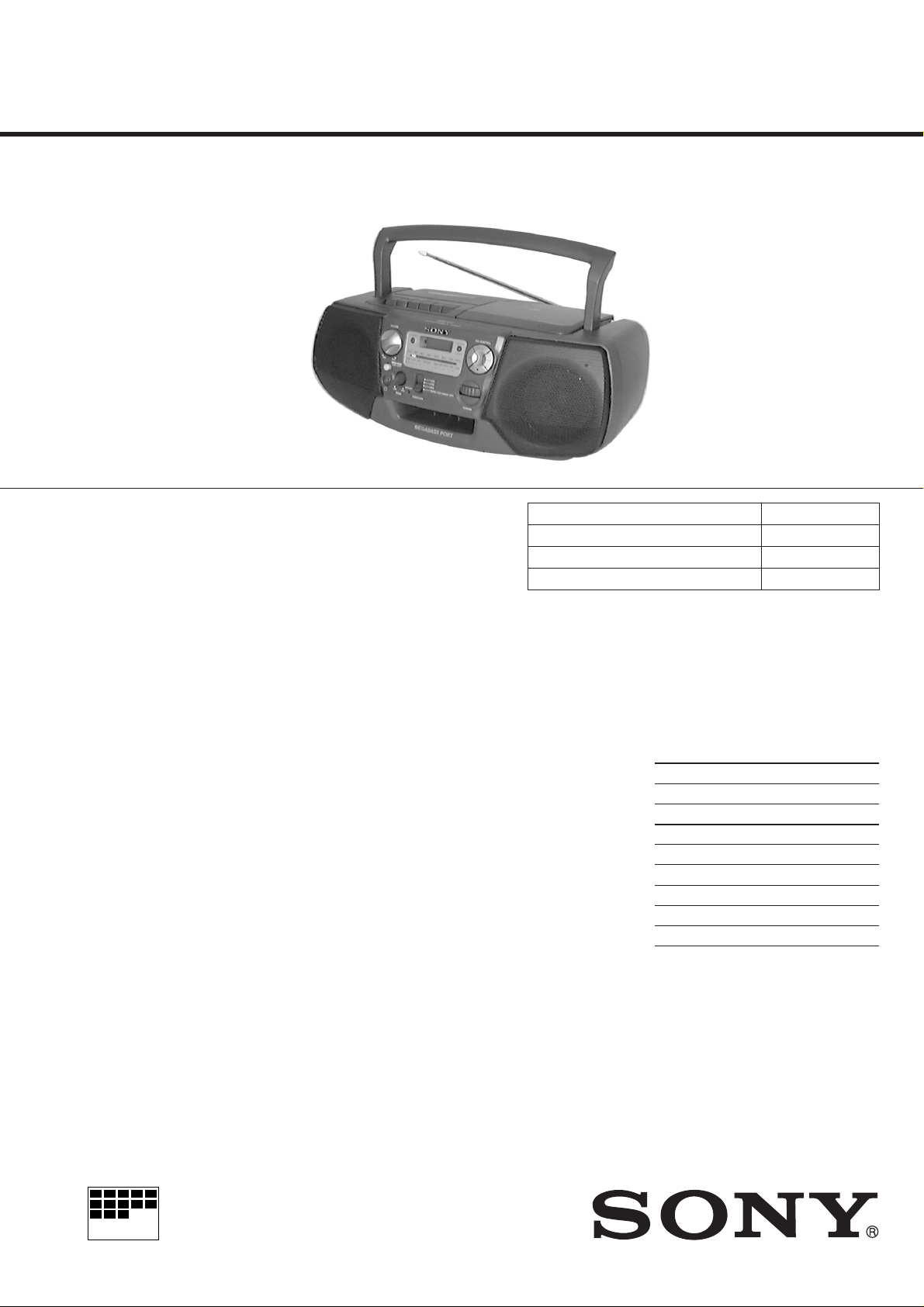
CFD-V17
SERVICE MANUAL
Ver 1.3 2000. 05
With SUPPLEMENT-1
(9-926-916-81)
SPECIFICATIONS
AUDIO POWER SPECIFICATIONS
POWER OUTPUT AND TOTAL HARMONIC DISTORTION
With 3.2 Ω loads, both channels driven from 150 – 10,000 Hz; rated 1.8
W per channel-minimum RMS power, with no more than 10 % total
harmonic distortion in AC operation.
Other Specifications
CD player section
System Compact disc digital audio system
Laser diode properties Material: GaAlAs
Wavelength:780 nm
Emission duration : Continuous
Laser output : Less than 44.6 µW
(This output is the value measured at a
distance of about 200 mm from the objective
lens surface on the optical pick-up block
with 7 mm aperture.)
Spindle speed 200 r/min (rpm) to 500 r/min (rpm) (CLV)
Number of channels 2
Frequency response 20 – 20,000 Hz + 1/-2 dB
Wow and flutter Below measurable limit
Radio section
Frequency range FM : 87.6 – 108 MHz
AM : 530 – 1,605 kHz (Australian model)
AM : 530 –1,710 kHz (Others models)
Aerials FM : Telescopic antenna
AM : Built-in ferrite bar aerial
Cassette-corder section
Recording system 4 -track 2 channel stereo
Fast winding time Approx. 120 s (sec.) with Sony cassette C-60
Frequency response TYPE I (normal) : 70 – 10,000 Hz
US Model
Canadian Model
E Model
Australian Model
Model Name Using • Similar Mechanism CFD-V15/V24
CD Mechanism Type KSM-213CDM
Optical Pick-up Type KSS-213CDM
T ape Transport Mechanism Type MF-V10-117
Power output (excluding US model)
2.3 W + 2.3 W (at 3.2 Ω, 10 % harmonic
distortion)
Power requirements For CD radio cassette-corder :
120V AC, 60 Hz
9V DC, 6 size D (R 20) batteries
Power consumption AC 20W
Battery life For CD radio cassette-corder:
FM recording
Sony R20P : approx. 13.5 h
Sony alkaline LR20 : approx. 20 h
Tape playback
Sony R20P : approx. 7.5 h
Sony alkaline LR20 : approx. 15 h
CD playback
Sony R20P : approx. 2.5 h
Sony alkaline LR20 : approx. 7 h
Dimensions Approx. 420 × 165 × 256 mm (w/h/d)
(16 5/8 × 6 1/2 × 10 1/8 inches) (incl. projecting
parts)
Mass Approx. 4.1 kg (9 lb. 1 oz) (incl. batteries)
Supplied accessories AC power cord (1)
Design and specifications are subject to change without notice.
General
Speakers Full range : 10 cm dia., 3.2 Ω, cone type (2)
Outputs Headphones jack (stereo minijack)
For 16 – 68 Ω impedance headphones
MICROFILM
CD RADIO CASSETTE-CORDER
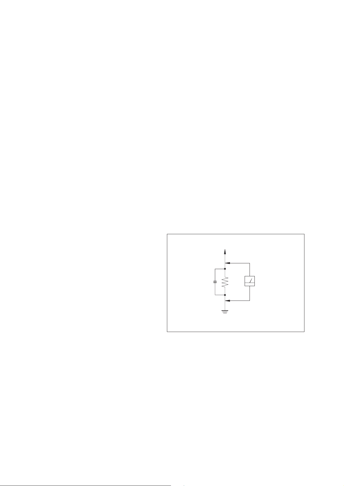
TABLE OF CONTENTS
1. SERVICE NOTES···························································· 3
SAFETY CHECK-OUT
2. GENERAL ··········································································4
3. DISASSEMBLY
3-1. Front Cabinet Assy ····························································· 5
3-2. Control Board ····································································· 6
3-3. Cabinet (upper) Assy··························································6
3-4. Inlet, Power, Battery, Half Battery Board···························7
3-5. Main Board·········································································7
3-6. Mechanism Deck, Optical Pick-up Section························8
4. DIAL POINTER INSTALLATION ·······························9
5. ADJUSTMENT
5-1. Mechanical Adjustment ···················································· 10
5-2. Electrical Adjustment ······················································· 10
5-3. Tuner Section···································································· 11
5-4. Reference·········································································· 15
6. DIAGRAM
6-1. Circuit Board Location ····················································· 17
6-2. Block Diagram ································································· 18
6-3. Printed Wiring Board························································ 21
6-4. Schematic Diagram – Main Section(1/2) – ······················ 25
6-5. Schematic Diagram – Main Section(2/2) – ······················ 30
6-6. Explanation of IC Terminals ············································ 33
7. EXPLODED VIEWS·················································38
After correcting the original service problem, perform the following
safety checks before releasing the set to the customer:
Check the antenna terminals, metal trim, “metallized” knobs, screws,
and all other exposed metal parts for A C leakage. Check leakage as
described below.
LEAKAGE
The AC leakage from any exposed metal part to earth ground and
from all exposed metal parts to any exposed metal part having a
return to chassis, must not exceed 0.5 mA (500 microamperes).
Leakage current can be measured by any one of three methods.
1. A commercial leakage tester, such as the Simpson 229 or RCA
WT -540A. Follo w the manufacturers’ instructions to use these
instruments.
2. A battery-operated AC milliammeter. The Data Precision 245
digital multimeter is suitable for this job.
3. Measuring the voltage drop across a resistor by means of a
VOM or battery-operated AC v oltmeter . The “limit” indication
is 0.75 V, so analog meters must have an accurate low-v olta ge
scale. The Simpson 250 and Sanwa SH-63Trd are e xamples of
a passive VOM that is suitable. Nearly all battery operated
digital multimeters that have a 2V AC range are suitable. (See
Fig. A)
8. ELECTRICAL PARTS LIST ··································· 44
T o Exposed Metal
Parts on Set
AC
0.15
µ
F
Fig. A. Using an A C v oltmeter to check A C leakage.
SAFETY-RELATED COMPONENT WARNING!!
COMPONENTS IDENTIFIED BY MARK ! OR DO TTED LINE WITH
MARK ! ON THE SCHEMATIC DIAGRAMS AND IN THE PARTS
LIST ARE CRITICAL TO SAFE OPERATION. REPLACE THESE
COMPONENTS WITH SONY PARTS WHOSE PART NUMBERS
APPEAR AS SHOWN IN THIS MANUAL OR IN SUPPLEMENTS
PUBLISHED BY SONY.
1.5 k
Ω
Earth Ground
Voltmeter
(0.75 V)
— 2 —
ATTENTION AU COMPOSANT AYANT RAPPORT
À LA SÉCURITÉ!
LES COMPOSANTS IDENTIFÉS P AR UNE MARQUE ! SUR LES
DIAGRAMMES SCHÉMA TIQUES ET LA LISTE DES PIÈCES SONT
CRITIQUES POUR LA SÉCURITÉ DE FONCTIONNEMENT. NE
REMPLACER CES COMPOSANTS QUE PAR DES PIÈSES SONY
DONT LES NUMÉROS SONT DONNÉS DANS CE MANUEL OU
DANS LES SUPPÉMENTS PUBLIÉS PAR SONY.
SECTION 1
Insert a precision screw driver
and push SWITCH(S801)
SERVICE NOTES
Laser component in this product is capable
of emitting radiation exceeding the limit for
Class 1.
This appliance is classified as a CLASS 1 LASER product. The
CLASS 1 LASER PRODUCT MARKING is located on the rear
exterior.
The following caution label is located inside the unit.
NOTES ON HANDLING THE OPTICAL PICK-UP
BLOCK OR BASE UNIT
The laser diode in the optical pick-up block may suffer electrostatic
breakdown because of the potential difference generated by the
charged electrostatic load, etc., on clothing and the human body.
During repair, pay attention to electrostatic breakdown and also use
the procedure in the printed matter which is included in the repair
parts.
The flexible board is easily damaged and should be handled with
care.
NOTES ON LASER DIODE EMISSION CHECK
The laser beam on this model is concentrated so as to be focused on
the disc reflective surface by the objective lens in the optical pickup block. Therefore, when checking the laser diode emission,
observe from more than 30 cm away from the objective lens.
CHUCK PLATE JIG ON REPAIRING
On repairing CD section, playing a disc without the CD lid, use
Chuck Plate Jig.
• Code number of Chuck Plate Jig : X-4918-255-1
CAUTION
Use of controls or adjustments or performance of procedures
other than those specified herein may result in hazardous radiation
exposure.
LASER DIODE AND FOCUS SEARCH OPERATION
CHECK
1. Press CD open knob.
2. Open the lid for CD.
3. Push on SWITCH (S801) as following figure.
4. Confirm the laser diode emission while observing the objecting
lens. When there is no emission, Auto Po wer Control circuit or
Optical Pick-up is broken.
Objective lens moves up and down once for the focus search.
— 3 —
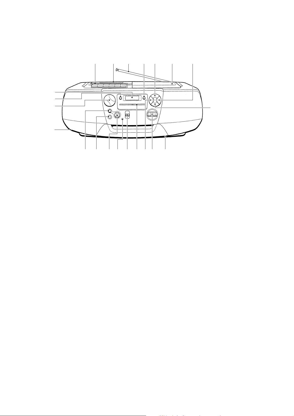
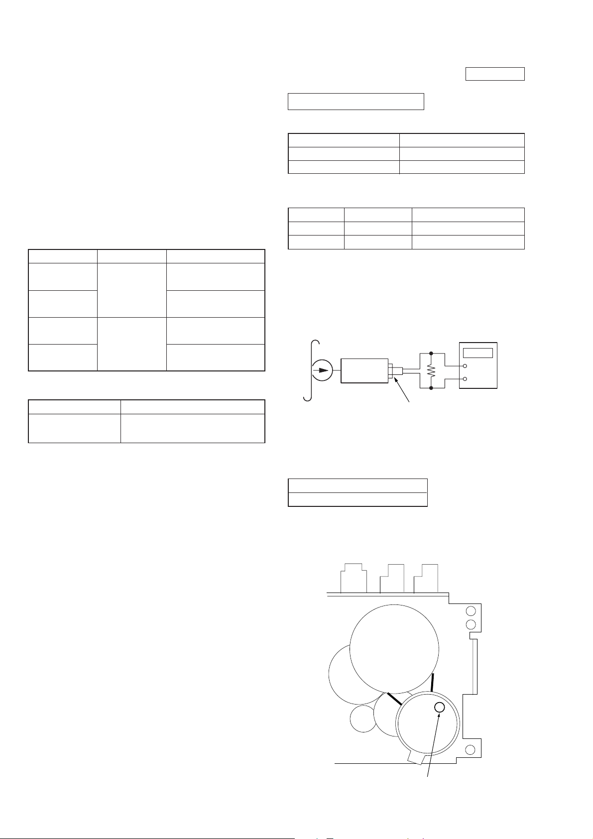
LOCATION AND FUNCTION OF CONTROLS
MAIN UNIT
SECTION 2
GENERAL
1
23
@¡
@º
!ª
!•
1 Tape operation buttons
r button
· button
0 button
) button
p, 6 button
P button
2 CASSETE LID
3 FM rod antenna
4 DISPLAY ENTER button
5 CD ^ button
6 CD 6 PUSH OPEN/CLOSE button
7 CD + button
8 CD p button
4
56
!™!£!¢!∞!§!¶
!¡
9 Battery compartment
!º TUNE knob
!¡ CD = button
!™ DIAL
!£ FUNCTION switch
!¢ OPR/BATT indicator
!∞ TONE knob
!§ 2 Phones jack
!¶ MEGA BASS knob
!• AC IN Socket
!ª VOLUME knob
@º PLAY MODE button
@¡ Information display
90
7
8
— 4 —
SECTION 3
DISASSEMBLY
• The equipment can be removed using the following procedure.
Front cabinet assySet
Cabinet (upper) assy
Control board
Inlet, power, battery, half battery board
Main board Mechanism deck, optical pick-up section
Note : Follow the disassembly procedure in the numerical order given.
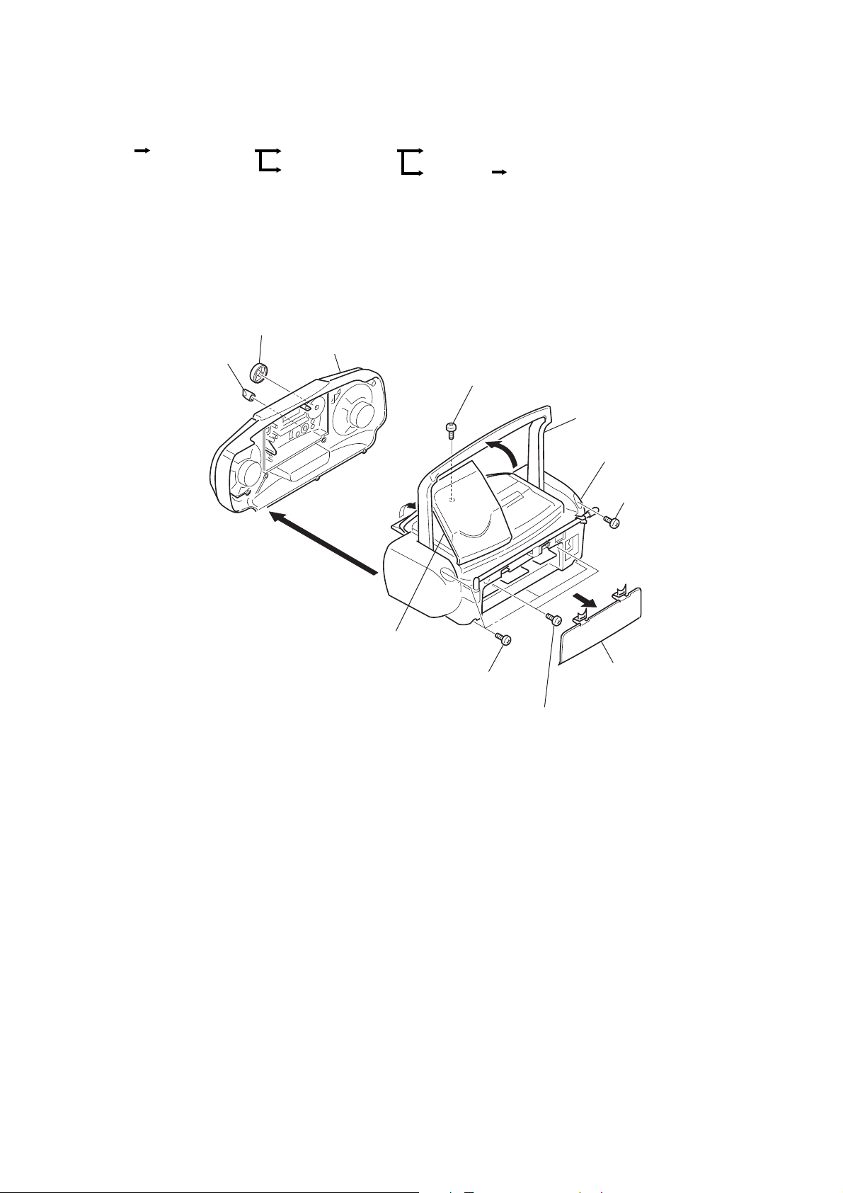
3-1. FRONT CABINET ASSY
8
Knob (Vol )
0
9
Knob (Tone)
Front cabinet assy
7
+BVTP 3
Screw
×
10
5
Remove the Handle
in the direction of the arrow.
Rear cabinet assy
4
Screw
+BVTP 3
×
10
6
Open the Lid (CD) in
the direction of the arrow.
3
Four screws
+BVTP 3
×
10
2
T wo screws
+BVTP 3
1
Lid, battery case
×
10
— 5 —
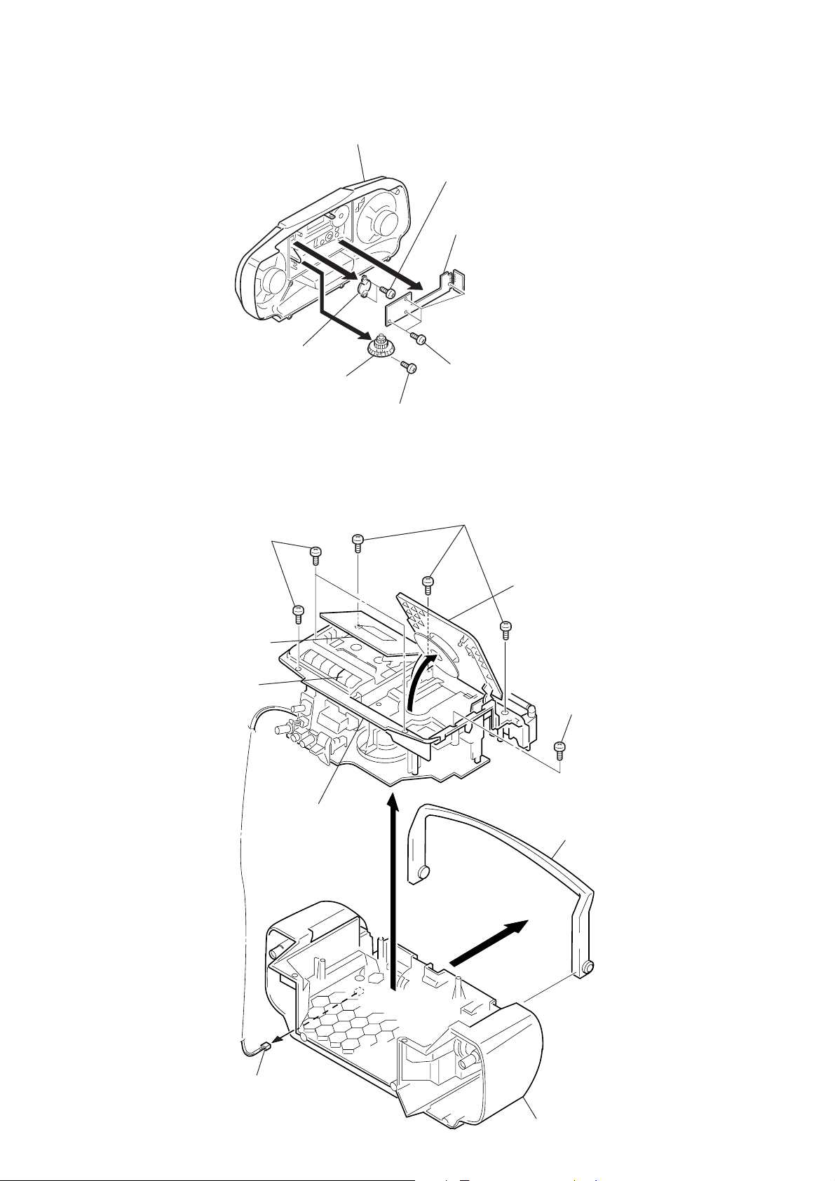
3-2. CONTROL BOARD
d
3-3. CABINET (UPPER) ASSY
Three screws
5
+BVTP 3
6
Button (CD)
×
10
4
Knob (TU)
7
Cabinet (Front) sub assy
5
T wo screws
+BVTP 2.6
3
Screw
×
8
2.6
×
8
2
CONTROL boar
1
Four screws
×
8
2.6
1
Three screws
+BVTP 3
×
10
2
Open the Holder assy, cassette by
pressing STOP/EJECT button.
STOP/EJECT
button
8
Cabinet (upper) assy
7
3
Open the Lid (CD) in
the direction of the arrow.
4
Screw
+BVTP 3
9
Open the Handle in
the direction of the arrow.
×
10
6
Connector
Rear cabinet
— 6 —
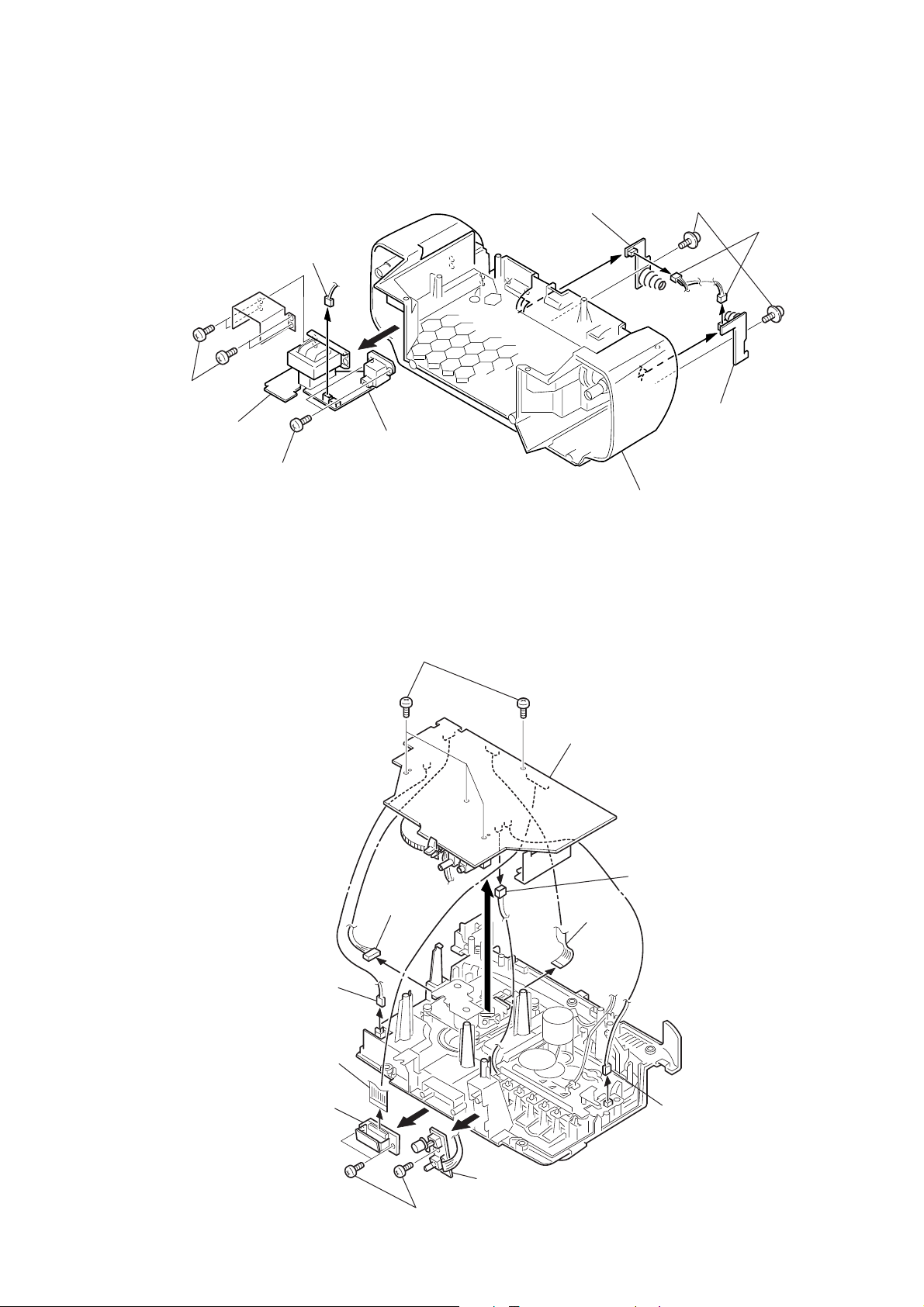
3-4. INLET, POWER, BATTERY, HALF BATTERY BOARD
r
5
Connector
1
Four screws
+BVTP 3 × 10
4
POWER board
2
T wo screws
+BVTP 3 × 10
3
INLET board
8
BATTERY board
6
T wo screws
+BVTP 3 × 8
9
Rear cabinet
7
T wo connectors
HALF BATTERY
board
3-5. MAIN BOARD
!¡
Connector
5
Four screws
+BVTP 3 × 10
0
Connector
6
!™
MAIN board
8
Flexible
9
Connector
3
Flexible
4
DISPLAY
board
2
1
Three Screws
+BVTP 3 × 10
— 7 —
VOLUME board
7
Connecto
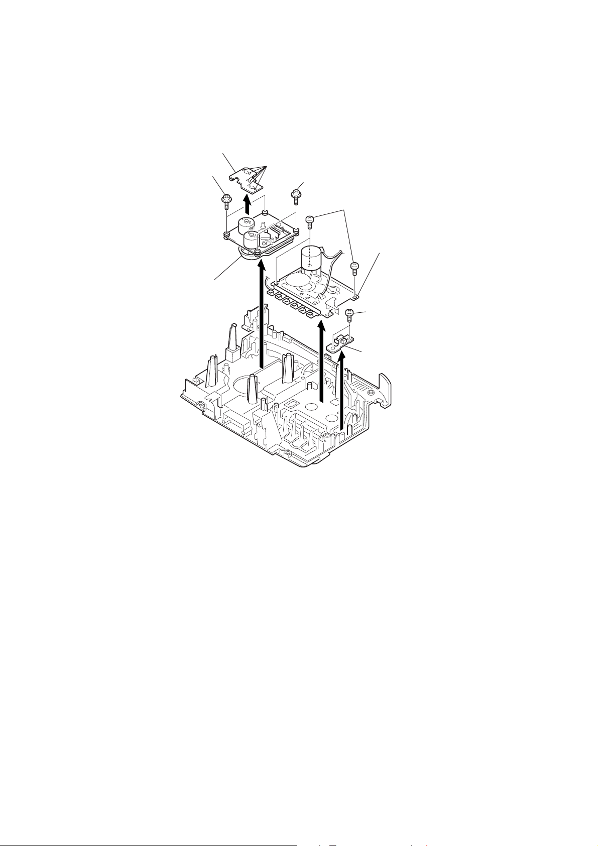
3-6. MECHANISM DECK, OPTICAL PICK-UP SECTION
0
8
CD MOTOR board
7
6
T wo screws
9
Optical pick-up section
Remove solder
5
T wo screws
3
+BVTP 3
Three screws
×
10
4
Mechanism deck
1
+BVTP 3
2
RECORD
switch board
T wo screws
×
1
— 8 —
SECTION 4
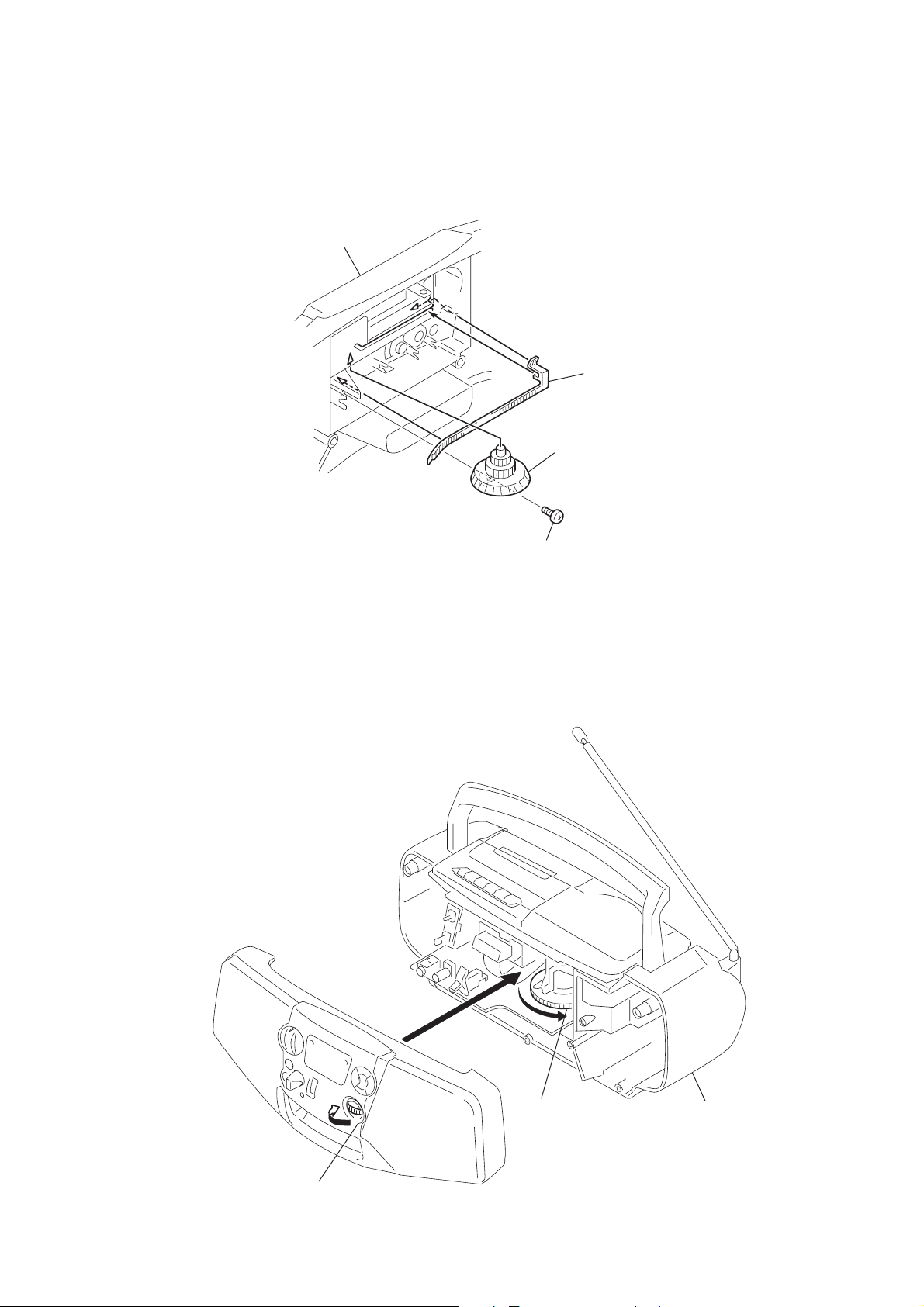
t
DIAL POINTER INSTALLATION
Note : Follow the installation procedure in the numerical order given.
1 Align the pointer with the groove of front cabinet and insert it as shown in the illustration.
2 Align Tuning knob with front cabinet and fasten the screw.
Front Cabinet
1
Pointer
Tuning knob B
2
Screw (2.6 × 8)
3 Turn the Tuning knob in the direction of the arrow as shown in the illustration until pointer agrees with scale “ 0 ” (at leftmost end of
scale).
4 Turn the tuning capacitor gear fully in the direction of the arrow as shown in the illustration.
5 Fasten the front cabinet and rear cabinet with the screws.
3
T uning knob
5
4
— 9 —
Tuning capacitor gear
Rear cabine
SECTION 5
ADJUSTMENTS
5-1. MECHANICAL ADJUSTMENT
PRECAUTION
1. Clean the following parts with a denatured-alchool-moistened
swab:
record/playback head pinch roller
erase head rubber belts
capstans
2. Demagnetize the record/playback head with a head
demagnetizer. (Do not bring the head demagnetizer close to
the erase head.)
3. Do not use a magnetized screwdriver for the adjustments.
4. After the adjustments, apply suitable locking compound to the
parts adjusted.
Torque Measurement
Mode
FWD
FWD
back tension
Fast Forward
Rewind
T ape Tension Measurement
Torque Meter
CQ-102C
CQ-201B
Meter Reading
18 – 60 g•cm
(0.25 – 0.83 oz•inch)
1.0 – 5.0 g•cm
(0.014 – 0.069 oz•inch)
45 – 95 g•cm
(0.62 – 1.32 oz•inch)
45 – 95 g•cm
(0.62 – 1.32 oz•inch)
5-2. ELECTRICAL ADJUSTMENT
TAPE RECODER SECTION
Standard output level
Output
Load impedance
Output signal level
Test tape
T est Tape
WS-48A
P-4-A063
Tape Speed Adjustment
Procedure :
Mode : Playback
test tape
WS-48A
(3kHz, 0dB)
Signal
3 kHz, 0 dB
6.3 kHz, –10 dB
set
0.25 V (–10 dB)
Tape speed adjustment
Head azimuth adjustment.
32
Ω
0dB = 0.775V
HP OUT
32 Ω
Used for
digital frequency
counter
+
–
Torque Meter
CQ-403A
Meter Reading
more than 60 g
(more than 2.12 oz)
J301 (phones)
Adjustment V alue : normal tape speed
Adjust the tape speed adjustment control inside motor, so that the
frequency counter reading becomes 3,000 Hz.
Specification Value :
Digital frequency counter
2,910 – 3,090Hz
Frequency difference between the beginning and the end of the
tape should be within 1.5% (45 Hz).
Adjustment Location :
— 10 —
Tape speed adjustment
control inside motor
5-3. TUNER SECTION
r
• Switch Location
VOLUME : MAX
MEGA BASS : OFF
PRESET SOUND MODE : OFF
AM SECTION
BAND : AM
Signal generator
AM RF signal
generator
Put the lead-wire
antenna close to
the set.
0 dB = 1 µV
• Repeat the procedures in each adjustment several times for the
maximum level meter indication.
• The frequency coverage and tracking adjustments should be
finally done by the trimmer capacitors.
AM IF ADJUSTMENT
Adjust for a maximum reading on level meter.
T2 455 kHz
AM TRACKING ADJUSTMENT
Adjust for a maximum reading on level meter.
L3 620 kHz
CT3 1,400 kHz
30% amplitude modulation by 400Hz
signal.
Output level : as low as possible
FM SECTION
BAND : FM
Signal generator
FM RF signal
generator
75kHz (100%) amplitude modulation
by 1kHz signal.
Output level : as low as possible
set
0.01µF
32
Ω
telescopic
antenna
terminal
level mete
+
–
AM FREQUENCY COVERAGE ADJUSTMENT
Adjust for a maximum reading on level meter.
L4 520 kHz (516 kHz)
CT4 1,780 kHz (1,605 kHz)
( ): Australian
FM IF ADJUSTMENT
Adjust for a maximum reading on level meter.
T1 10.7 MHz
FM TRACKING ADJUSTMENT
Adjust for a maximum reading on level meter.
L1 86.5 MHz
CT1 109.5 MHz
FM FREQUENCY COVERAGE ADJUSTMENT
Adjust for a maximum reading on level meter.
L2 86.5 MHz
CT2 109.5 MHz
Adjustment Location : Main board (See page 13)
J301 (phones)
— 11 —
FM VCO Adjustment
l
color
mark
CF1
r
Procedure :
FM RF SSG
0.01µF
to ANT IN termina
Carrier frequency : 98MHz
IF frequency : According to
the color of CF1.
Modulation : no modulation
Output level : 0.1V (100dB)
1. Connect frequency counter to the positions shown below.
2. Tune the set to 98MHz.
3. Adjust RV1 so that the frequency counter reading becomes
75,000 Hz.
Specification Value :
Frequency counter
75,950 – 76,050 Hz
Frequency counte
IC1 Pin
IC1 Pin
4
7
0.01µF
33k
Ω
+
–
RED 10.70MHz
BLUE 10.67MHz
ORANGE 10.73MHz
BLACK 10.64MHz
WHITE 10.76MHz
Adjustment Location : MAIN board (See page 13)
— 12 —
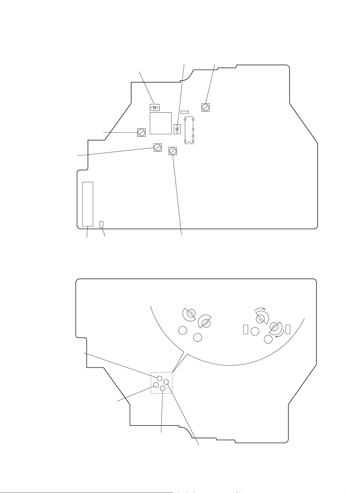
Adjustment Location : MAIN board (Component side)
L1
FM T rac king
Adjustment
L4
AM Frequency
Coverage
Adjustment
RV1
FM VCO
Adjustment
CV1
L2
FM Frequency
Coverage
Adjustment
CF1
15
16
7
4
1
30
IC1
T2
AM IF
Adjustment
L3
FM ANT IN
AM T rac king
Adjustment
Adjustment Location : MAIN board (Conductor side)
CT4
AM Frequency
Coverage
Adjustment
CT3
AM T rac king
Adjustment
T1
FM IF
Adjustment
Set the CT2 (FM OSC) and CT4 (AM OSC)
trimmers to their extreme outside.
AM OSC
AM OSC
FM OSC
Inside NG Outside OK
FM OSC
CT1
FM T rac king
Adjustment
— 13 —
CT2
FM Frequency
Coverage
Adjustment
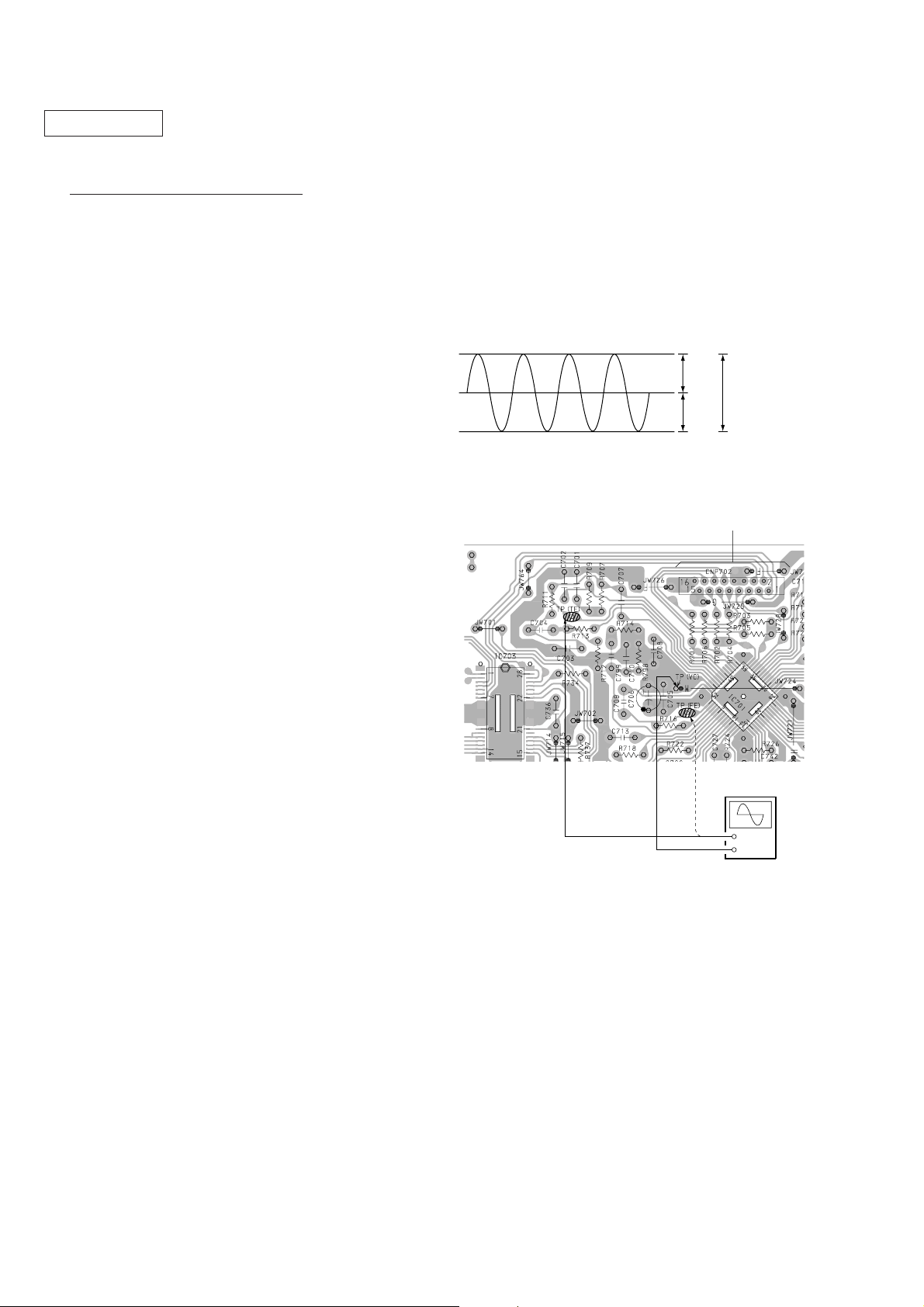
CD SECTION
V
s
Notes on Check
1. Perform the traverse check in the CD test mode.
After check, be sure to exit the test mode.
2. Perform check in the order given.
3. Use the disc (YEDS-18, Parts No. 3-702-101-01) only when
so indicated.
Before Check
Put the set into test mode and perform the following checks.
Repair if there are any problems.
• Sled Motor Check
Press + , = keys and confirm that the Optical pick-up moves
smoothly from the innermost to outermost circumference and back
smoothly and with no catching or abnormal noises.
(Cancellation of BTL mute)
+ : Optical pick-up moves to the outer circumference.
= : Optical pick-up moves to the inner circumference.
• Focus Search Check
1. Press the CD ^ key. (Focus search operation is performed
continuously.)
2. Look at the Optical pick-up objective lens and confirm that it
moves up and down smoothly, with no catching or abnormal
noises.
3. Press p button.
Confirm that focus search operation stops. If it does not, press
p button again longer.
TRAVERSE Check
This check is to be done when the optical pick-up block is replaced.
Check Procedure:
1. Connect the oscilloscope to test point TP (VC) and TP (TE) on
MAIN board.
2. Put the set into test mode.
3. Optical pick-up setting to the center by + or = button
pushing.
4. Insert disk (YEDS-18) and press ^ button.
5. Check that the oscilloscope traverse waveform is symmetrical,
as shown in the figure below.
6. Release test mode after adjustment is completed.
A
VOLT/DIV : 0.1
0V
TIME/DIV : 1m
B
A = B C = 300mV – 700mV
C
[MAIN BOARD] (Conductor side)
How to Enter the Set into Test Mode
1. Set the function switch to power off.
2. Set the function switch to CD while = key and p key
pressing.
The set is into CD test mode (88 is displayed).
3. Turn the power off to release test mode.
How to Exit the Test Mode
Turn the POWER OFF.
TP (TE)
TP (FE)
TP (VC)
Oscilloscope
(DC range)
+
–
— 14 —
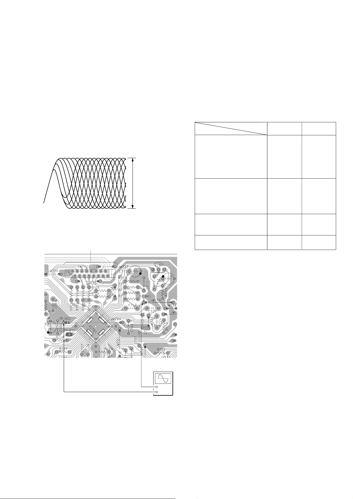
Focus Bias Check
s
This check is to be done when the optical block replaced.
Check Procedure:
1. Connect the oscilloscope to test point TP (VC) and TP (RF) on
MAIN board.
2. Put the set into test mode.
3. Opitical pick-up setting to the center by + or – button pushing.
4. Insert disk (YEDS-18) and press ^ button.
5. Press the MODE button. (Tracking servo ON)
6. Check that the oscilloscope wavewform is as sho wn in the figure
below (eye pattern).
A good eye pattern means that the diamond shape (◊) in the
center of the waveform can be clearly distinguished.
7. Release test mode after adjustment is completed.
• RF signal reference waveform (eye pattern)
VOLT/DIV : 0.2V
TIME/DIV : 500n
0.9Vp-p – 1.3Vp-p
When observing the eye pattern, set the oscilloscope for AC range
and raise vertical sensivity.
[MAIN BOARD] (Conductor side)
5-4. REFERENCE
Focus/Tracking Gain Check
Adjustment Location : MAIN board (Component side)
(See page 16)
A frequency response analyzer is necessary in order to perform this
check exactly.
However , this gain has a mar gin, so e ven if it is slightly of f, there is
no problem.
Focus/Tracking gain determines the pick-up follo w-up (vertical and
horizontal) relative to mechanical noise and mechanical shock when
the 2-axis device operate.
Symptoms
Gain
• The time until music starts
becomes longer for STOP ➡
CD ^ or automatic
selection (0 , ) buttons
pressed). (Normally takes
about 2 seconds.)
• Music does not start and disc
continues to rotate for STOP
➡ CD ^ or automatic
selection (0 , ) buttons
pressed.)
• Sound is interrupted during
PLAY. Or time counter
display stops progressing.
• More noise during 2-axis
device operation.
Focus
low
—
—
high
Tracking
low or high
low
low
high
TP
(RF)
TP(VC)
Check Procedure:
1. Keep the set horizontal.
2. Inset disk (YEDS-18) and press ^ button.
3. Connect an oscilloscope to TP (FE) and TP (VC) on the MAIN
board.
4. Check that the waveform is as sho wn in the figure below . (Focus
waveform)
Oscilloscope
(DC range)
+
–
— 15 —
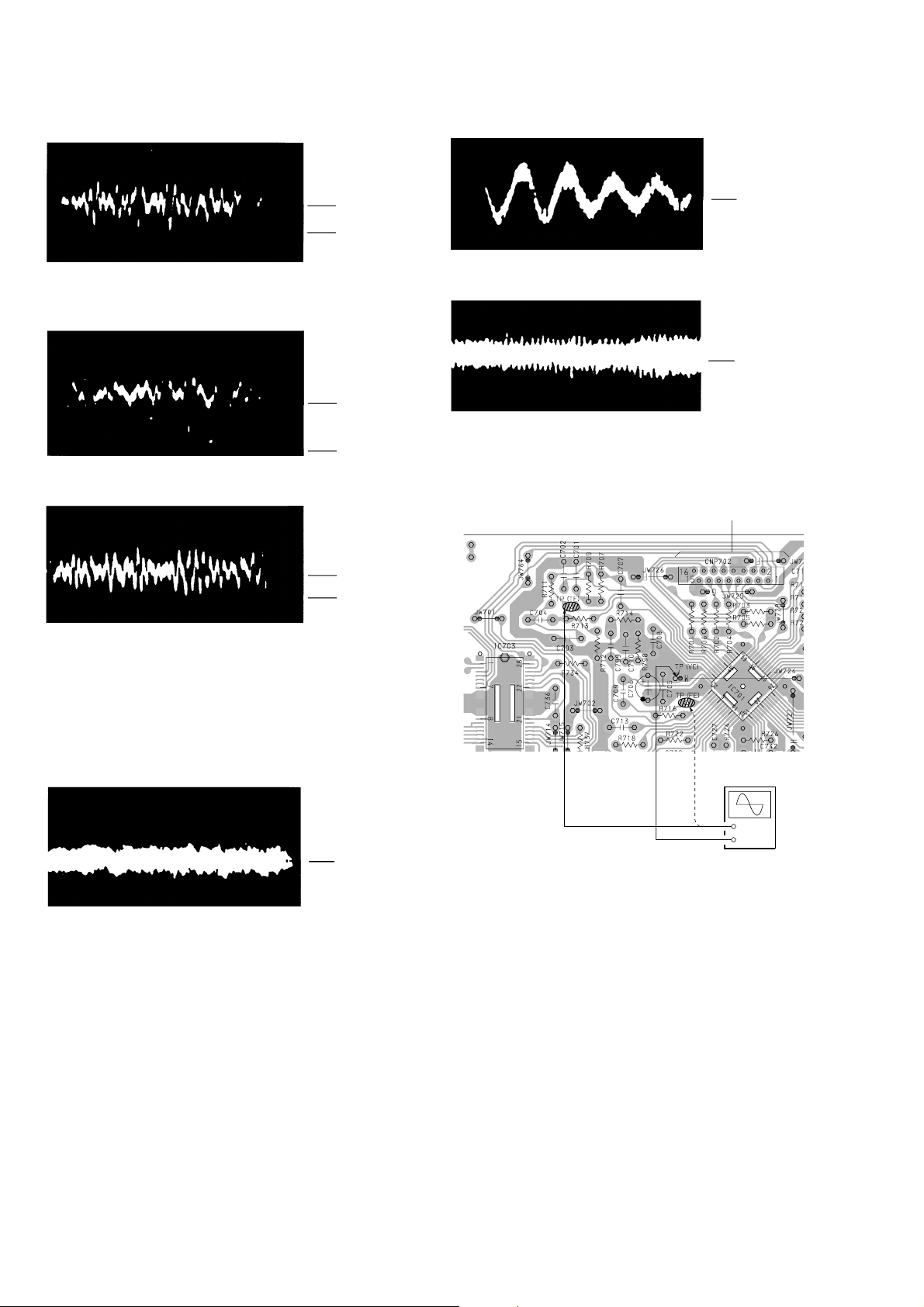
• Good Example
V
V
V
V
V
V
• Incorrect Examples (Fundamental wave appears)
VOLT/DIV : 100m
TIME/DIV : 1ms
100mV
0V
• Incorrent Examples (DC level changes more than on adjusted
waveform)
VOLT/DIV : 100m
TIME/DIV : 2ms
200mV
0V
low focus gain
VOLT/DIV : 100m
TIME/DIV : 2ms
75mV
0V
VOLT/DIV : 0.2
TIME/DIV : 2ms
0V
low tracking gain
VOLT/DIV : 0.2
TIME/DIV : 2ms
0V
high tracking gain
(high fundamental wave than for low gain)
[MAIN BOARD] (Conductor side)
high focus gain
5. Connect an oscilloscope between TP (TE) and TP (VC).
6. Insert disc (YEDS-18) and press the CD ^ button.
7. Check that the waveform is as shown in the figure below.
(tracking waveform)
VOLT/DIV : 0.2
TIME/DIV : 2ms
0V
TP (TE)
TP (FE)
TP (VC)
Oscilloscope
(DC range)
+
–
— 16 —
SECTION 6
d
DIAGRAMS
CFD-V17
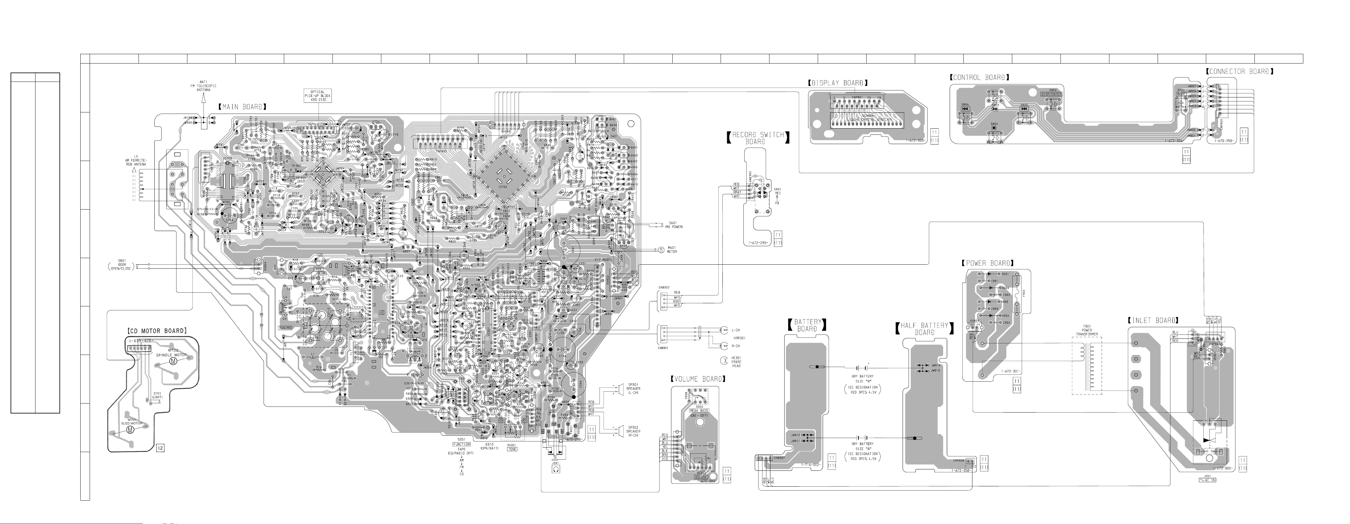
6-1. CIRCUIT BOARDS LOCATION
RECORD SWITCH board
INLET board
POWER board
VOLUME board
DISPLAY board
CONTROL board
CONNECTOR board
BATTERY board
MAIN board
HALF BATTERY board
CD MOTOR boar
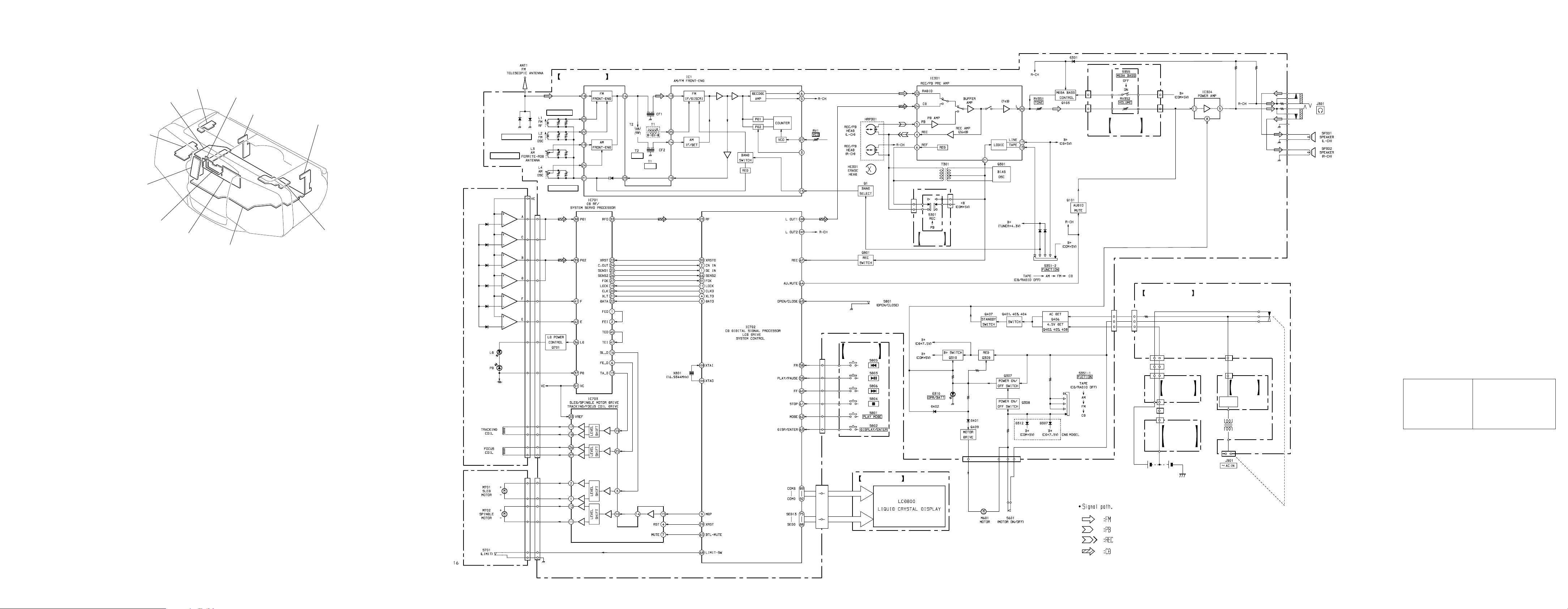
6-2. BLOCK DIAGRAM
FM F-COVERAGE
L3, CT3
AM TRACKING
OPTICAL PICK-UP
BLOCK
(KSS-213CDM)
L2, CT2
CNP702
12
10
11
13
9
14
7
5
3
2
4
1
CNB701
3
4
1
2
5
6
MAIN BOARD
L1, CT1
FM TRACKING
L4, CT4
AM F-COVERAGE
AM IF
FM IF
KH803
CNP803
7
6
5
4
3
2
CNP802 CNP801
1-4
5-18
CONTROL
BOARD
LCD BOARD
CNB302
CNJ302
4
3
RECORD
SWITCH
BOARD
CNJ302
CNB302
1
KH308
KH307
1 2
2 4
KH306
KH307
KH307 KH308
KH307 KH306
VOLUME
BOARD
Note on Printed Wiring Board:
• X : parts extracted from the component side.
• Y : parts extracted from the conductor side.
• b : Pattern from the side which enables seeing.
Note on Schematic Diagrams:
• All capacitors are in µF unless otherwise noted. pF: µµF
50 WV or less are not indicated except for electrolytics
INLET BOARD
KH902
3
2
4
3
2
4
CNP902
CNP907
31
CNJ907
1
3
31
CNB907
BATTERY
BOARD
CNB907
4
4
CNB908
4
CNB908
HALF
RECT
D901-904
KH902
2
KH904
2
POWER
BOARD
T901
POWER
TRANSFORMER
BATTERY
BOARD
4
3
CNP304
21
CNJ304
DRY BATTERY
SIZE "D"
(IEC DESIGNATION R20)
6PCS. 9V
and tantalums.
• All resistors are in Ω and 1/
specified.
¢
•
: internal component.
4
W or less unless otherwise
• 2 : nonflammable resistor.
• C : panel designation.
• H : adjustment for repair.
• U : B+ Line.
• Power voltage is dc 9 V and fed with regulated dc power
supply from battery terminal.
• Voltages and waveforms are dc with respect to ground
under no-signal (detuned) conditions.
Note:
The components identified by mark ! or dotted
line with mark ! are critical for safety.
Replace only with part
number specified.
Note:
Les composants identifiés par
une marque ! sont critiques
pour la sécurité.
Ne les remplacer que par une
piéce portant le numéro
spécifié.
– For Radio, TAPE section MAIN (1/2) –
no mark : PLAY (TAPE SECTION)
CD STOP
( ) : REC (TAPE SECTION)
[ ] : FM (RADIO SECTION)
< > : AM (RADIO SECTION)
– For CD Section MAIN (2/2) –
no mark : CD PLAY
TAPE STOP
• Voltages are taken with a V OM (Input impedance 10 MΩ).
Voltage variations may be noted due to normal production tolerances.
• Signal path.
F : FM
E : PB
a : REC
J : CD
• Abbreviation
CND : Canadian
MX : Mexican
AUS : Australian
— 17 — — 18 — — 19 — — 20 —
CFD-V17
6-3. PRINTED WIRING BOARD • Refer to page 20 for Note on Printed Wiring Board.
• Semiconductor
Location
Ref. No. Location
D1 G-6
D2 G-6
D301 G-10
D302 D-10
D303 G-8
D304 G-8
D307 E-8
D308 D-8
D309 G-7
D310 H-9
D312 F-8
D311 D-11
D314 G-7
D401 C-11
D402 C-12
D403 B-11
D404 B-11
D406 C-11
D407 C-11
D408 C-11
D409 C-12
D410 C-12
D411 C-12
D801 D-7
IC1 F-7
IC301 F-9
IC304 E-11
IC701 C-5
IC702 C-9
IC703 C-3
Q1 G-7
Q101 F-10
Q102 G-8
Q103 G-9
Q201 E-10
Q202 G-9
Q203 G-9
Q301 E-9
Q307 D-11
Q308 C-11
Q309 D-11
Q310 E-8
Q401 B-12
Q402 B-12
Q403 B-12
Q404 B-11
Q405 C-12
Q406 C-11
Q407 B-11
Q408 C-11
Q409 D-12
Q701 B-6
Q801 D-7
A
B
C
D
E
F
G
12
345678910111213141516171819202122232425
CND MODEL
CND MODEL
REC/PB
HEAD
H
+
16
I
— 21 — — 22 — — 23 — — 24 —
 Loading...