

SONY CFD S550, CFD S55 Service Manual
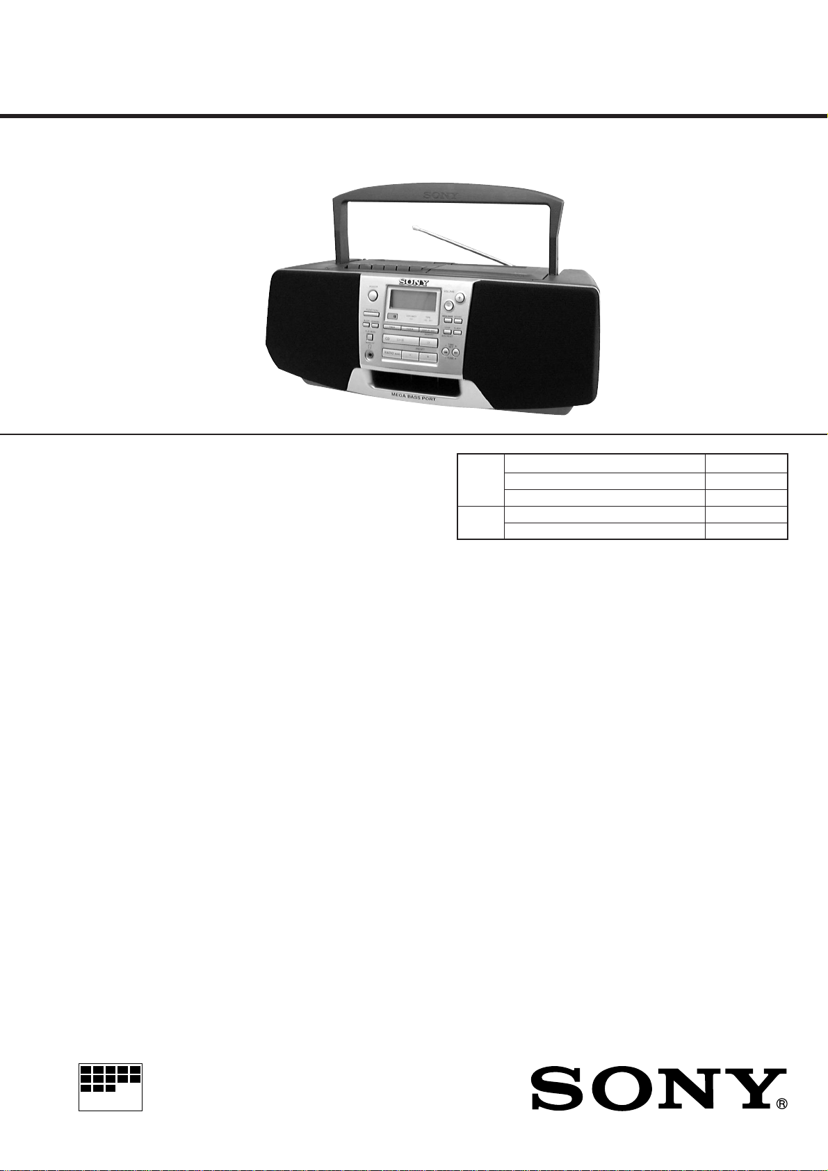
CFD-S39
SERVICE MANUAL
Ver 1.0 1999. 05
CD
Section
TC
Section
US Model
Model Name Using Similar Mechanism CFD-S38
CD Mechanism Type KSM-213CDM
Optical Pick-up Name KSS-213C
Model Name Using Similar Mechanism NEW
Tape Transport Mechanism Type MF-B7S-148
AUDIO POWER SPECIFICATIONS
POWER OUTPUT AND TOTAL
HARMONIC DISTORTION
With 6-ohm loads, both channels driven from
100 - 10,000 Hz; rated 4 W per channelminimum RMS power, with no more than 10%
total harmonic distortion in AC operation.
Other Specifications
CD player section
System
Compact disc digital audio system
Laser diode properties
Material: GaAlAs
Wave length: 780 nm
Emission duration: Continuous
Laser output: Less than 44.6 µW
(This output is the value measured at a distance of
about 200 mm from the objective lens surface on
the optical pick-up block with 7 mm aperture.)
Spindle speed
200 r/min (rpm) to 500 r/min (rpm) (CLV)
Number of channels
2
Frequency response
20 - 20,000 Hz +1/–2 dB
Wow and flutter
Below measurable limit
SPECIFICATIONS
Radio section
Frequency range
FM: 87.6 - 108 MHz
AM: 530 - 1,710 kHz
Aerials
FM: Telescopic aerial
AM: Built-in ferrite bar aerial
Cassette-corder section
Recording system
4-track 2 channel stereo
Fast winding time
Approx. 90 sec. with Sony cassette C-60
Frequency response
TYPE I (normal): 70 - 13,000 Hz
General
Speaker
Full range: 10 cm (4 in.) dia.,
6 ohms, cone type (2)
Outputs
Headphones jack (stereo minijack)
For 16 - 68 ohms impedance headphones
– Continued on next page –
MICROFILM
CD RADIO CASSETTE-CORDER
– 1 –
CFD-S39
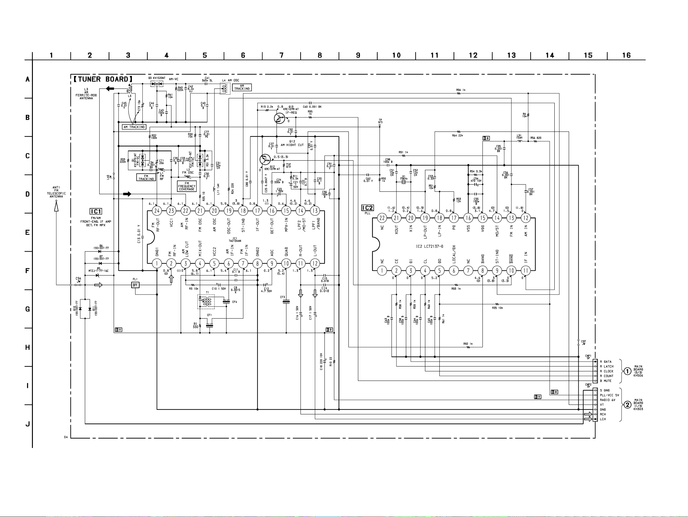
6-5. SCHEMATIC DIAGRAM — TUNER SECTION — • Refer to page 41 for IC Block Diagrams.
Note:
• All capacitors are in µF unless otherwise noted. pF: µµF
50 WV or less are not indicated except for electrolytics
and tantalums.
• All resistors are in Ω and 1/
specified.
¢
•
• U : B+ Line.
: internal component.
4
W or less unless otherwise
– 23 – – 24 –
• H : adjustment for repair.
• Power voltage is dc 9 V and fed with regulated dc power
supply from battery terminal.
• Voltage and waveforms are dc with respect to ground
under no-signal (detuned) conditions.
no mark : FM
( ) : AM
(Page 33)
(Page 29)
• V oltages are taken with a V OM (Input impedance 10 MΩ).
Voltage variations may be noted due to normal production tolerances.
• Signal path.
F : FM
f : AM
6-9. SCHEMATIC DIAGRAM — MAIN SECTION (1/3) — • Refer to page 41 for IC Block Diagrams.
CFD-S39
(Page 39)
• Semiconductor Location
Ref. No. Location
D302 C-5
D303 H-5
D351 D-3
D501 E-6
D502 E-7
D590 D-7
D591 E-7
D951 H-5
D952 H-5
D953 I-4
D955 H-5
D957 I-5
IC301 F-5
IC303 I-7
IC304 I-8
Ref. No. Location
IC501 C-8
IC502 D-6
IC503 B-10
IC701 H-13
IC702 H-11
IC703 E-13
Q301 C-5
Q311 F-9
Q312 F-10
Q313 G-10
Q321 C-6
Q322 C-5
Q323 C-5
Q324 C-5
Q325 C-4
Ref. No. Location
Q326 C-5
Q501 D-8
Q502 D-8
Q503 C-12
Q505 B-10
Q506 B-10
Q701 I-12
Q951 G-4
Q952 H-4
Q953 I-4
Q954 H-4
Q955 I-4
Q957 I-5
Q958 E-4
Q959 E-4
Q960 D-5
– 29 –
(Page 24)
(Page 32)
Note on Printed Wiring Boards:
• X : parts extracted from the component side.
• b : Pattern from the side which enables seeing.
(Page 33)
(Page 38)
Note on Schematic Diagram:
• All capacitors are in µF unless otherwise noted. pF: µµF
50 WV or less are not indicated except for electrolytics
and tantalums.
• All resistors are in Ω and 1/
specified.
• C : panel designation.
• U : B+ Line.
• Power voltage is dc 9 V and fed with regulated dc power
supply from battery terminal.
4
W or less unless otherwise
– 30 –
• Voltage and waveforms are dc with respect to ground
under no-signal (detuned) conditions.
no mark : TAPE PB
( ) : TAPE REC
• V oltages are taken with a V OM (Input impedance 10 MΩ).
Voltage variations may be noted due to normal production tolerances.
• Signal path.
F : FM
E : T APE PB
a : TAPE REC
 Loading...