

Page 1
Page 2
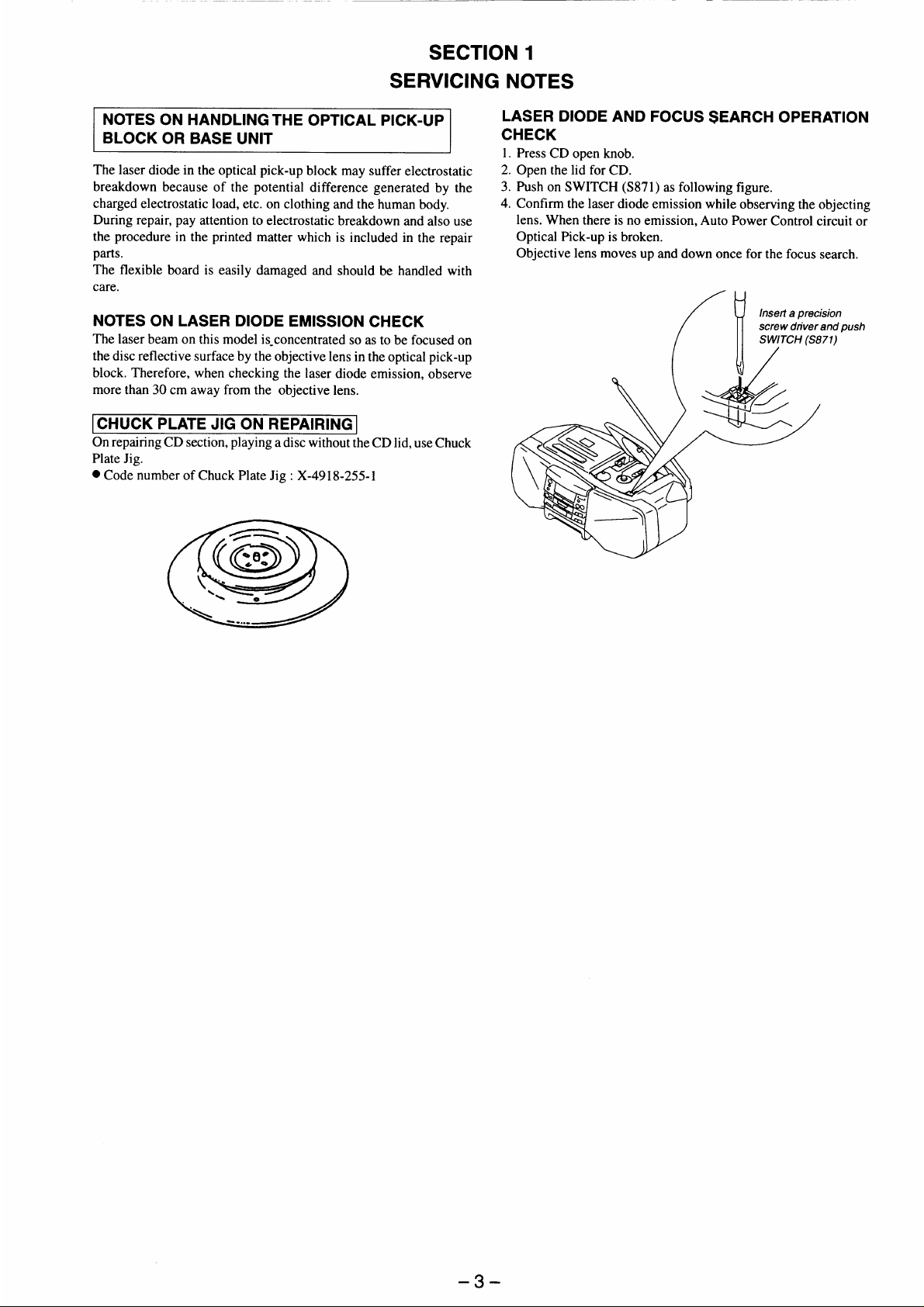
Page 3
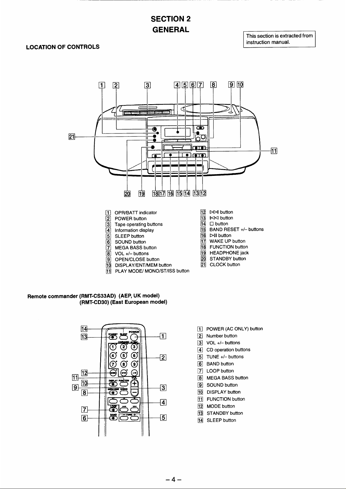
Page 4
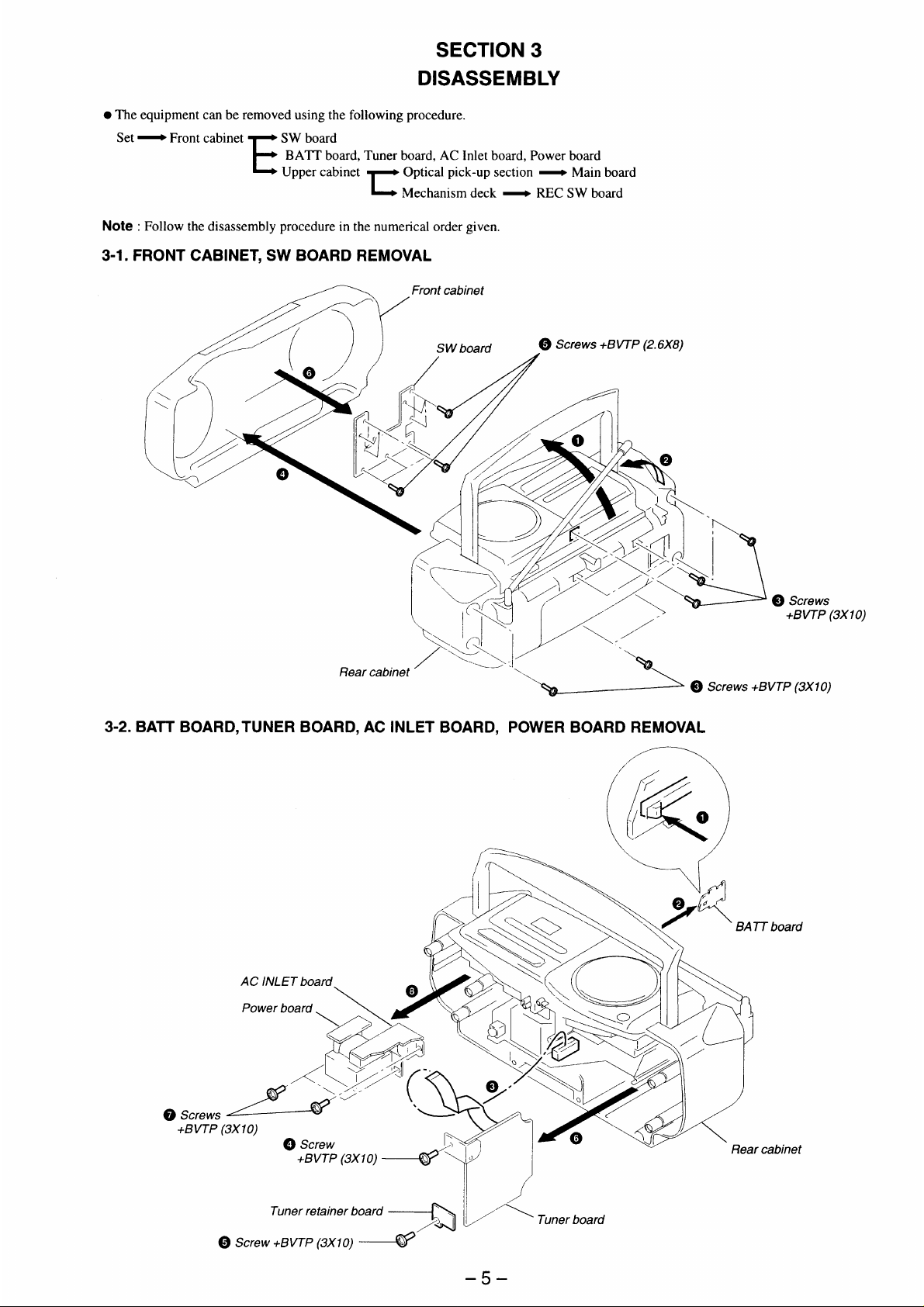
Page 5
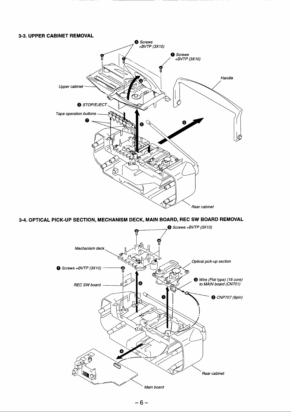
Page 6
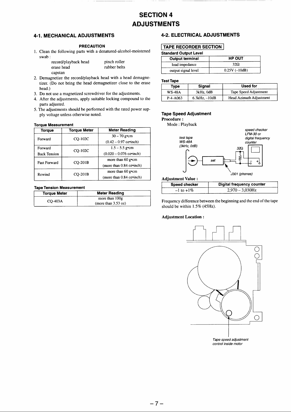
Page 7
Page 8
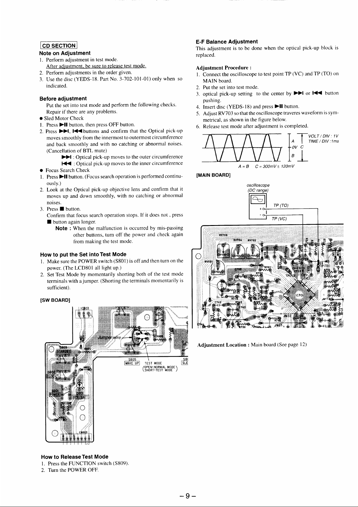
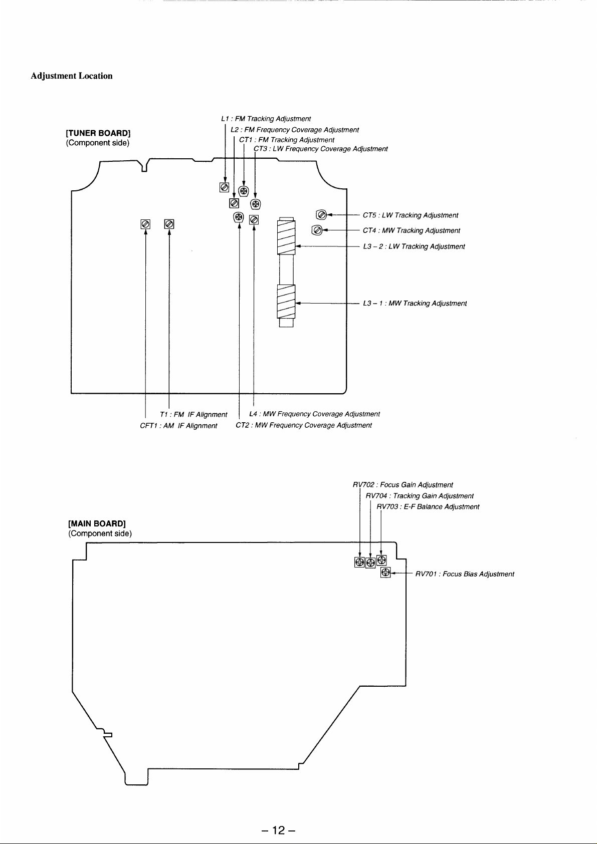
Page 9
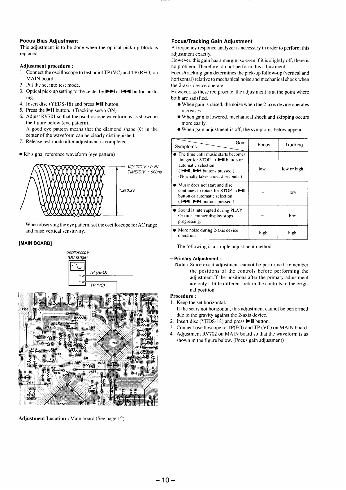
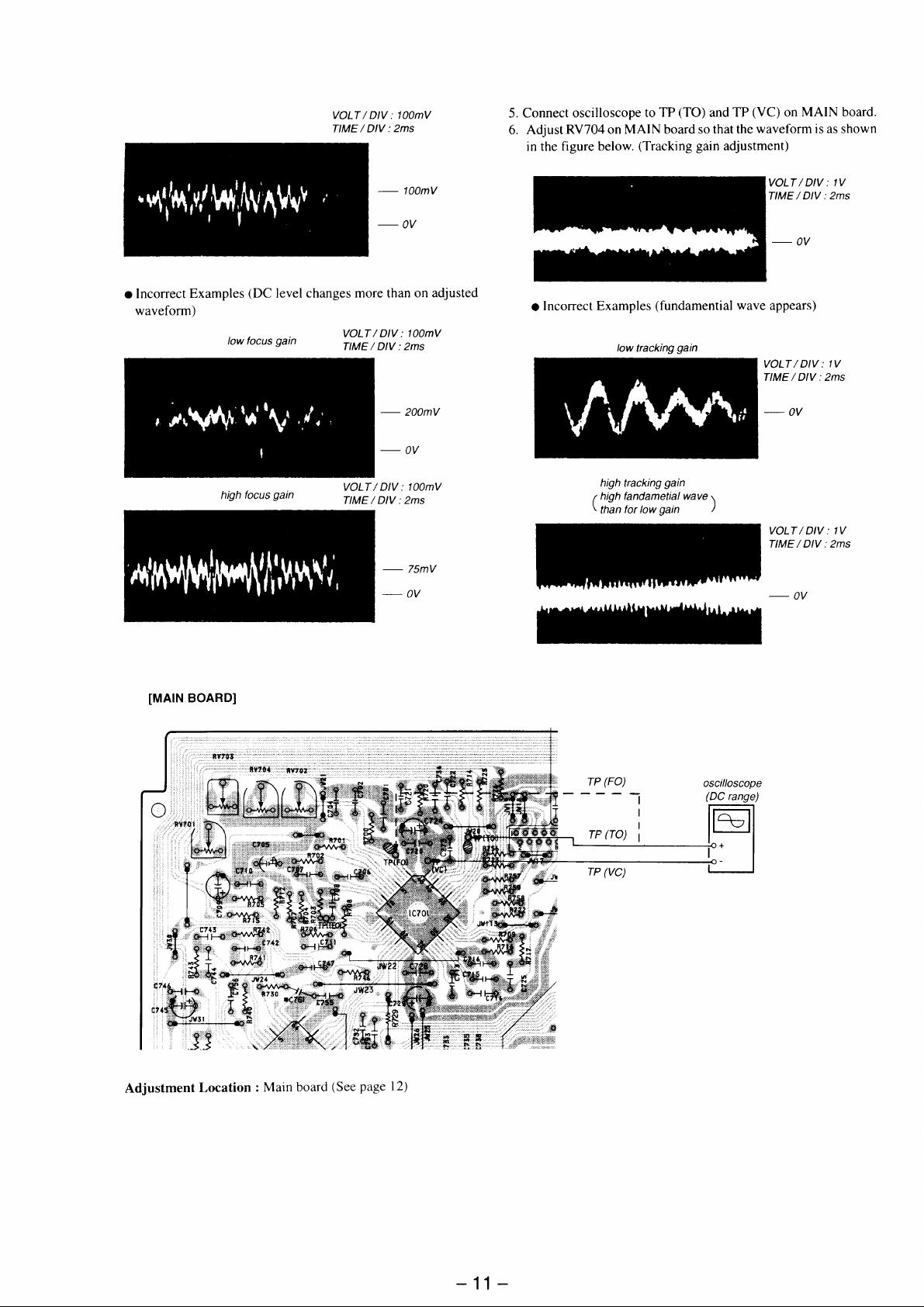
Page 10
Page 11
Page 12
Page 13
Page 14
Page 15

Page 16

Page 17

Page 18

Page 19

Page 20

Page 21

Page 22

Page 23

Page 24

Page 25

Page 26

Page 27

Page 28

Page 29

Page 30

Page 31

Page 32

Page 33

SERVICE MANUAL
Ver 1.0 1998. 08
SUPPLEMENT - 1
File this Supplement with the Service Manual.
Subject :
r
CHANGE OF BOARDS
AC INLET BOARD : 1-666-267-11 / 1-666-267-12
BATT BOARD : 1-666-266-11 / 1-666-266-12
MAIN BOARD : 1-666-263-11 / 1-666-263-12
POWER BOARD : 1-666-264-11 / 1-666-264-12
REC SW BOARD : 1-666-265-11 / 1-666-265-12
r
CHANGE OF OPTICAL PICK-UP BLOCK
KSM-213CAM / KSM-213CDM
r
CHANGE OF EXPLODED VIEWS
CFD-S33L
AEP Model
UK Model
(SPM-97033)
Page 34

r
CHANG OF BOARDS
The main boar d, po wer boar d, BA TT boar d, REC SW boar d, and A C inlet boar d ha ve been c hang ed.
Changed printed wiring boards and schematic diagram, and changed parts list are described in this Supplement-1.
Refer to original ser vice man ual (9-923-173-11) pre viousl y issued f or the other inf ormation.
NEW TYPE IDENTIFICA TION
[MAIN BOARD] (Component side)
[BATT BOARD]
(Component side)
1-666-266
-12
1-666-263
[AC INLET BOARD]
(Component side)
1-666-267
-12
-12
[POWER BOARD]
(Component side)
1-666-264
-12
[REC SW BOARD]
(Component side)
1-666-265
-12
– 2 –
Page 35

CHANGE OF ELECTRICAL PARTS LIST
M
MAIN
(Service Manual See page 39 to 42)
Before Change After Change
Ref. No. Part No. Description Part No. Description Remark
C303 –––––––––––
C316 1-136-165-00 FILM 0.1uF 5% 50V
C334 –––––––––––
C346 1-130-471-00 MYLAR 0.001uF 5% 50V
C398 1-162-282-31 CERAMIC 100PF 10% 50V
C716 1-136-169-00 FILM 0.22uF 5% 50V
C748 1-162-306-11 CERAMIC 0.01uF 20% 16V
C765 –––––––––––
C766 –––––––––––
C767 –––––––––––
C788 1-162-306-11 CERAMIC 0.01uF 20% 16V
C821 1-162-306-11 CERAMIC 0.01uF 20% 16V
D301 8-719-010-55 DIODE UZ-7.5BSC
D310 –––––––––––
D804 8-719-987-63 DIODE 1N4148M
D815 –––––––––––
Q952 8-729-037-11 TRANSISTOR KTA1271Y-AT
R125 –––––––––––
R225 –––––––––––
R305 1-249-407-11 CARBON 150 5% 1/4W
R760 –––––––––––
R822 –––––––––––
R890 –––––––––––
R937 –––––––––––
R954 –––––––––––
R955 –––––––––––
R956 –––––––––––
R957 –––––––––––
S821 1-762-758-11 SWITCH, KEYBOARD (RESET)
1-162-306-11 CERAMIC 0.01uF 20% 16V
1-136-153-00 FILM 0.01uF 5% 50V
1-162-294-31 CERAMIC 0.001uF 10% 50V
1-130-475-00 MYLAR 0.0022uF 5% 50V
1-162-282-31 CERAMIC 100PF 10% 50V
(AEP,UK)
1-136-153-00 FILM 0.01uF 5% 50V
1-161-494-00 CERAMIC 0.022uF 25V
1-162-282-31 CERAMIC 100PF 10% 50V
1-162-306-11 CERAMIC 0.01uF 20% 16V
1-162-306-11 CERAMIC 0.01uF 20% 16V
1-161-494-00 CERAMIC 0.022uF 5% 25V
1-124-903-11 ELECT 1uF 20% 50V
8-719-110-04 DIODE RD7.5ES-B3
8-719-991-33 DIODE 1SS133T-77
–––––––––––
8-719-991-33 DIODE 1SS133T-77
8-729-040-76 TRANSISTOR KTA1273-Y-AT
1-249-435-11 CARBON 33K 5% 1/4W
1-249-435-11 CARBON 33K 5% 1/4W
1-249-406-11 CARBON 120 5% 1/4W
1-249-417-11 CARBON 1K 5% 1/4W
1-249-393-11 CARBON 10 5% 1/4W
1-249-429-11 CARBON 10K 5% 1/4W
1-249-421-11 CARBON 2.2K 5% 1/4W
1-249-417-11 CARBON 1K 5% 1/4W
1-249-429-11 CARBON 10K 5% 1/4W
1-249-417-11 CARBON 1K 5% 1/4W
1-249-417-11 CARBON 1K 5% 1/4W
1-762-871-11 SWITCH, KEYBOARD (RESET)
Added
Changed
Added
Changed
Changed
Changed
Changed
Added
Added
Added
Changed
Changed
Changed
Added
Deleted
Added
Changed
Added
Added
Changed
Added
Added
Added
Added
Added
Added
Added
Added
Changed
TUNER
(Service Manual See page 43 to 45)
• Abbreviation
EE : East European
Before Change After Change
Ref. No. Part No. Description Part No. Description Remark
1-162-199-31 CERAMIC 10PF 5% 50V (EE)
(EE)
(EE)
(EE)
Changed
Changed
Changed
Changed
Changed
Changed
Changed
Added
Added
Added
Changed
Changed
Changed
Added
Changed
Changed
Changed
Changed
Changed
C4 1-162-203-31 CERAMIC 15PF 5% 50V
(AEP,UK)
C8
C23 1-161-052-00 CERAMIC 0.012uF 10% 25V
C24 1-161-052-00 CERAMIC 0.012uF 10% 25V
C48 1-162-207-31 CERAMIC 22PF 5% 50V
C61 1-162-306-11 CERAMIC 0.01uF 20% 16V
C63 1-162-294-31 CERAMIC 0.001uF 10% 50V
C71 ––––––––––––––
C72 ––––––––––––––
C73 ––––––––––––––
L1 0-435-499-20 COIL, FM RF (EE)
L2 0-435-500-20 COIL, FM OSC (EE)
L4 0-432-881-30 COIL, MW/LW OSC
L7 ––––––––––––––
R33 1-249-409-11 CARBON 220 5% 1/4W
R39 1-249-429-11 CARBON 10K 5% 1/4W
R40 1-249-421-11 CARBON 2.2K 5% 1/4W
R62 1-249-426-11 CARBON 5.6K 5% 1/4W
R64 1-249-426-11 CARBON 5.6K 5% 1/4W
1-162-195-31 CERAMIC 4.7PF 10% 50V
(AEP,UK)
1-162-203-31 CERAMIC 15PF 5% 50V
1-162-195-31 CERAMIC 4.7PF 10% 50V
1-161-053-00 CERAMIC 0.015uF 10% 25V
1-161-053-00 CERAMIC 0.015uF 10% 25V
1-162-201-31 CERAMIC 12PF 5% 50V
1-162-306-11 CERAMIC 0.01uF 20% 16V
(AEP,UK)
1-130-489-00 MYLAR 0.033uF 5% 50V (EE)
1-162-294-31 CERAMIC 0.001uF 10% 50V
(AEP,UK)
1-162-300-21 CERAMIC 0.01uF 30% 16V (EE)
1-162-282-31 CERAMIC 100PF 10% 50V
1-162-282-31 CERAMIC 100PF 10% 50V
1-162-294-31 CERAMIC 0.001uF 10% 50V
1-406-995-41 COIL, FM RF (EE)
1-406-994-41 COIL, FM OSC (EE)
1-411-199-31 COIL, MW/LW OSC
1-414-137-21 INDUCTOR, MICRO 0.22uH (EE)
1-249-402-11 CARBON 56 5% 1/4W
1-249-409-11 CARBON 220 5% 1/4W
(AEP, UK)
1-249-417-11 CARBON 1K 5% 1/4W
1-249-429-11 CARBON 10K 5% 1/4W
(AEP, UK)
1-249-417-11 CARBON 1K 5% 1/4W
1-249-421-11 CARBON 2.2K 5% 1/4W
(AEP, UK)
1-247-843-11 CARBON 3.3K 5% 1/4W
1-247-843-11 CARBON 3.3K 5% 1/4W
r
CORRECTION
Page
34,45
35,45 ! T901 1-426-632-11 TRANS FORMER, POWER
Ref. No. Part No. Description Remark Part No. Description Remark
55 1-452-899-11 MAGNET
56 3-923-498-01 PLATE, CHUCK
! 1-751-214-11 CORD, POWER (UK)
45
! ––––––––––––
INCORRECT CORRECT
The components identified by mark !
or dotted line with mark ! are critical
for safety.
Replace only with part number specified.
3-923-498-01 PLATE, CHUCK
1-452-899-11 MAGNET
1-427-943-11 TRANS FORMER, POWER
1-696-820-21 CORD, POWER (UK)
1-770-019-11 ADAPTOR, CONVERSION PLUG (UK)
r
CHANGE OF OPTICAL PICK-UP BLOCK
KSM-213CAM n KSM-213CDM
Since the new chassis assy (MB) (RP), motor (including M702) and chucking plate are not compatible with the former ones, when
replacing either of these parts, replace them with the same version.
How to distinguish the sets
You can distinguish the sets by the optical pick-up type name printed on the optical pick-up block.
Optical pick-up
Former T ype : KSM-213CAM
New Type : KSM-213CD
Page 1
!
: changed portion
New T ypeFormer Type
Model Name Using CD Section
Similar Mechanism Tape Section
Optical Pick-up Type KSM-213CAM/C1NP
Tape Transport Mechanism Type MF-V10-117
NEW
DIFFERENCE PARTS LIST
Page
38,45 255 X-2625-770-1 CHASSIS ASSY (MB) (RP), MOTOR
Ref. No. Part No. Description Remark Part No. Description Remark
34 55 3-923-498-01 PLATE, CHUCK (FOR KSM-213CAM)
7-6. OPTICAL PICK-UP SECTION
38
(KSM-213CAM/C1NP)
Former Type New T ype
(INCLUDING M702) (SPINDLE)
÷
Model Name Using CD Section
Similar Mechanism Tape Section
Optical Pick-up Type KSM-213CDM
Tape Transport Mechanism Type MF-V10-117
3-019-395-01 PLATE, CHUCKING (FOR KSM-213CDM)
NEW
7-6. OPTICAL PICK-UP SECTION
(KSM-213CDM)
X-2626-202-1 CHASSIS ASSY (MB) (RP), MOTOR
(INCLUDING M702) (SPINDLE)
$
– 3 – – 4 – – 6 –– 5 –
Page 36

Page 37

r
p
p
SCHEMATIC DIAGRAM – MAIN SECTION (1/2) –
r
Waveforms
1
CFD-S33L
1.1 Vp-
75 kHz
IC2 1
(X OUT)
2
IC801 &™
(XTAL)
3
IC801 #º
(TX)
VOLT/DIV : 0.2 V AC
TIME/DIV : 10 µsec
3.6 Vp-
4.19 MHz
VOLT/DIV : 1 V AC
TIME/DIV : 0.1 µsec
4.4 Vp-p
32.768 kHz
VOLT/DIV : 1 V AC
TIME/DIV : 20 µsec
Note:
• All capacitors are in µF unless otherwise noted. pF: µµF
50 WV or less are not indicated except for electrolytics
and tantalums.
• All resistors are in Ω and 1/
specified.
Note: The components identified by mark ! or dotted
line with mark ! are critical for safety.
Replace only with part number specified.
• U : B+ Line.
• Power voltage is dc 9 V and fed with regulated dc power
supply from external power voltage jack.
• Voltages and waveforms are dc with respect to ground
under no-signal (detuned) conditions.
no mark : FM (Radio Section) PLAY (Tape Section)
( ) : AM (Radio Section) REC (Tape Section)
• Voltages and currents are taken with a VOM (Input impedance 10 MΩ).
Voltage variations may be noted due to normal production tolerances.
• Waveforms are taken with a oscilloscope.
Voltage variations may be noted due to normal production tolerances.
• Circled numbers refer to waveforms.
• Signal path.
F : FM
E : PB (L-CH)
d : PB (R-CH)
a : REC (L-CH)
G : REC (R-CH)
• Abbreviation
EE : East European
4
W or less unless otherwise
– 11 – – 12 – – 14 –– 13 –
Page 38

CFD-S33L
p
p
r
Waveforms
(PLAY MODE)
1
r
SCHEMATIC DIAGRAM – MAIN SECTION (2/2) –
4
1.0 – 1.4
Vp-p
IC701 #¡
(RFO)
VOLT/DIV : 0.2 V AC
TIME/DIV : 0.5 µsec
2 5
4.8 Vp-
IC702 @∞
(XPCK)
242.0 µsec
VOLT/DIV : 1 V AC
TIME/DIV : 0.1 msec
3 6
5.3 Vp-p
µ
sec
140.5
IC702 @•
(RFCK)
VOLT/DIV : 1 V AC
TIME/DIV : 50 µsec
140.5
IC702 #¡
(MNT3)
140.5
IC702 #™
(MNT1)
16.9344 MHz
IC702 #∞
(XTAO)
µ
sec
VOLT/DIV : 1 V AC
TIME/DIV : 50 µsec
µ
sec
VOLT/DIV : 1 V AC
TIME/DIV : 50 µsec
VOLT/DIV : 0.2 V AC
TIME/DIV : 50 nsec
5.3 Vp-p
5.3 Vp-p
1.1 Vp-
Note:
• All capacitors are in µF unless otherwise noted. pF: µµF
50 WV or less are not indicated except for electrolytics
and tantalums.
• All resistors are in Ω and 1/
specified.
Note: The components identified by mark ! or dotted
line with mark ! are critical for safety.
Replace only with part number specified.
• U : B+ Line.
• H : adjustment for repair.
• Power voltage is dc 9 V and fed with regulated dc power
supply from external power voltage jack.
• Voltages and waveforms are dc with respect to ground
under no-signal (detuned) conditions.
no mark : CD STOP
• Voltages are taken with a VOM (Input impedance 10 MΩ).
Voltage variations may be noted due to normal production tolerances.
• Waveforms are taken with a oscilloscope.
Voltage variations may be noted due to normal production tolerances.
• Circled numbers refer to waveforms.
• Signal path.
J : CD
4
W or less unless otherwise
– 17 – – 8 –– 15 – – 16 –
Page 39

r
CHANGE OF EXPLODED VIEWS (Service Manual See page 33 to 38)
NOTE :
• -XX, -X mean standardized parts, so they
may have some difference from the original
one.
• Color indication of Appearance Parts
Example :
KNOB, BALANCE (WHITE) ••• (RED)
↑↑
Parts color Cabinet's color
• Items marked “ * ”are not stocked since they
are seldom required for routine service. Some
delay should be anticipated when ordering
these items.
• The mechanical parts with no reference
number in the exploded views are not
supplied.
• Accessories and packing materials are given
in the last of this parts list.
• Abbreviation
EE : East European
7-1. FRONT CABINET SECTION
The components identified by mark !
or dotted line with mark ! are critical
for safety.
Replace only with part number specified.
#9
#1
SP901
#1
#1
3
#9
#9
#9
4
2
5
#1
4
SP902
#1
#9
C851
#1
6
1
Ref. No. Part No. Description Remark Ref. No. Part No. Description Remark
1 X-3373-392-1 NET (R) ASSY
2 X-3373-391-1 NET (L) ASSY
3 X-3373-952-1 CABINET(FRONT) ASSY (BLACK) (AEP,UK)
3 X-3373-972-1 CABINET(FRONT) ASSY (SILVER) (AEP,UK)
3 X-3373-953-1 CABINET(FRONT) ASSY (EE)
4 4-951-620-01 SCREW (2.6X8), +BVTP
* 5 1-665-045-11 SW BOARD
6 3-009-228-01 WINDOW, INDICATION
C851 1-162-199-31 CERAMIC 10PF 5% 50V
SP901 1-505-531-11 SPEAKER (10cm) (L-CH)
SP902 1-505-531-11 SPEAKER (10cm) (R-CH)
– 19 –
Page 40

7-2. UPPER CABINET SECTION
59
58
60
61
74
62
63
64
65
MF-V10-117
#1
#1
68
#10
57
#10
56
55
54
#6
#10
#2
#10
66
#1
67
78
69
KSM-213CDM
72
71
71
53
72
73
77
52
51
#1
Ref. No. Part No. Description Remark Ref. No. Part No. Description Remark
51 3-009-208-01 SPRING, CASSETTE UP
52 3-922-112-11 DAMPER
53 3-009-186-01 CABINET (UPPER) (BLACK)
53 3-009-186-31 CABINET (UPPER) (SILVER)
54 3-009-209-01 SPRING, CD UP
S871
76
75
63 3-009-197-21 BUTTON (FF) (SILVER) (AEP,UK)
64 3-009-200-01 BUTTON (STOP) (BLACK)
64 3-009-200-21 BUTTON (STOP) (SILVER) (AEP,UK)
65 3-009-195-01 BUTTON (PAUSE) (BLACK)
65 3-009-195-21 BUTTON (PAUSE) (SILVER) (AEP,UK)
70
55 3-019-395-01 PLATE, CHUCKING (FOR KSM-213CDM)
55 3-923-498-01 PLATE, CHUCK (FOR KSM-213CAM)
(FORMER TYPE)
56 1-452-899-11 MAGNET
57 3-009-187-01 LID, CD (BLACK)
57 3-009-187-31 LID, CD (SILVER)
58 X-3373-389-1 HOLDER SUB ASSY,CASSETTE (BLACK)
58 X-3373-975-1 HOLDER SUB ASSY,CASSETTE (SILVER)
* 59 3-009-206-01 SHAFT (MD)
60 3-009-196-01 BUTTON (REC) (BLACK)
60 3-009-196-21 BUTTON (REC) (SILVER) (AEP,UK)
61 3-009-199-01 BUTTON (PLAY) (BLACK)
61 3-009-199-21 BUTTON (PLAY) (SILVER) (AEP,UK)
62 3-009-198-01 BUTTON (REW) (BLACK)
62 3-009-198-21 BUTTON (REW) (SILVER) (AEP,UK)
63 3-009-197-01 BUTTON (FF) (BLACK)
(NEW TYPE)
– 20 –
66 4-951-620-01 SCREW (2.6X8), +BVTP
* 67 1-666-265-11 REC SW BOARD
68 3-009-201-01 HANDLE (BLACK)
68 3-009-201-21 HANDLE (SILVER) (AEP,UK)
69 3-923-736-01 COVER, CD
70 1-777-955-11 WIRE (FLAT TYPE) (16 CORE)
71 3-910-095-31 RUBBER, VIBRATION PROOF (RED)
72 3-910-095-21 RUBBER, VIBRATION PROOF (GREEN)
73 1-639-678-12 CD MOTOR BOARD
74 3-009-214-01 SPRING, REC
75 3-831-441-99 CUSHION, SPEAKER
76 3-015-646-01 CUSHION (CD)
77 3-923-151-01 CUSHION, RUBBER
78 3-018-078-01 SPACER (PICK)
S871 1-692-960-11 SWITCH, PUSH (1 KEY) (DOOR OPEN CLOSE)
Page 41

7-3. REAR CABINET SECTION
104
105
103
not supplied
ANT1
116
106
F902
T901
#1
113
not supplied
101
#1
LCD801
#1
115
#1
102
#7
#1
#1
113
112
111
114
107
108
116
#3
109
110
The components identified by mark !
or dotted line with mark ! are critical
for safety.
Replace only with part number specified.
Ref. No. Part No. Description Remark Ref. No. Part No. Description Remark
* 101 A-3306-324-A MAIN BOARD, COMPLETE (AEP,UK)
* 101 A-3306-659-A MAIN BOARD, COMPLETE (EE)
* 102 3-009-219-01 HOLDER, LCD
103 1-533-233-31 HOLDER, FUSE
* 104 1-666-264-11 POWER BOARD
* 105 1-666-267-11 AC INLET BOARD
106 3-013-719-21 CABINET (REAR) (EE)
106 3-013-719-41 CABINET (REAR) (BLACK) (AEP,UK)
106 3-013-719-51 CABINET (REAR) (SILVER) (AEP,UK)
107 3-009-211-01 SPRING (–)
* 108 1-666-266-11 BATT BOARD
109 3-009-210-01 SPRING (+/–)
110 3-009-202-01 LID, BATTERY CASE (BLACK)
110 3-009-202-21 LID, BATTERY CASE (SILVER)(AEP,UK)
* 111 3-009-222-01 TERMINAL (SYNTHESIZER), ANTENNA
* 112 A-3306-516-A TUNER BOARD, COMPLETE (AEP,UK)
* 112 A-3306-658-A TUNER BOARD, COMPLETE (EE)
113 3-703-397-01 STOPPER, WIRING
114 1-782-112-11 WIRE, PARALLEL (FFC) (13 CORE)
115 1-666-570-11 TUNER RETAINER BOARD
116 3-831-441-11 CUSHION (F)
ANT1 1-501-918-11 ANTENNA, TELESCOPIC
! F902 1-532-464-31 FUSE (T2.5AL/250V)
LCD801 1-801-592-11 DISPLAY PANEL, LIQUID CRYSTAL
! T901 1-427-943-11 TRANSFORMER, POWER
– 21 –
Page 42

7-4. MECHANISM DECK SECTION (1)
(MF-V10-117)
HRP901
159
155
153
157
154
HE901
158
169
156
151
168
160
167
161
162
170
163
164
165
166
152
Ref. No. Part No. Description Remark Ref. No. Part No. Description Remark
151 3-933-010-01 SPRING (S/P), TORSION
152 3-933-025-01 SPRING (P), TORSION
153 3-933-026-01 LEVER (P)
154 3-933-024-01 ROLLER, PINCH
155 3-933-019-01 SPRING (F/R), TORSION
156 3-933-028-01 SPRING (FWD), TORSION
157 3-933-016-01 GEAR (S REEL)
158 3-008-590-01 SLIDER (REC)
159 3-008-592-01 BASE (H), HEAD
* 160 3-008-588-01 SLIDER (REW)
* 161 3-008-589-13 SLIDER (FF)
* 162 3-008-587-01 SLIDER (STOP)
* 163 3-008-591-01 SLIDER (PAUSE)
164 3-933-004-01 CLAW, REEL
* 165 3-933-021-01 SLIDER (FRP)
* 166 3-933-006-01 SLIDER (EJECT)
167 3-934-833-01 SPRING (FRP)
168 3-022-794-02 SPRING (BT)
169 3-933-007-01 PLATE, LOCK
* 170 3-012-114-01 LEVER (FR)
HE901 1-543-876-11 HEAD (ERASE)
HRP901 1-500-454-11 HEAD,MAGNETIC (RECORD/PLAYBACK)
– 22 –
Page 43

7-5. MECHANISM DECK SECTION (2)
(MF-V10-117)
207
M901
S902
204
#6
206
S901
203
205
218
208
220
209
210
219
211
212
213
217
214
#4
202
Ref. No. Part No. Description Remark Ref. No. Part No. Description Remark
201 3-933-029-01 LEVER, ERASING PREVENTION
202 3-933-182-01 SPRING, CASSETTE
203 3-932-995-01 GEAR (MID)
204 X-3371-667-1 CLUTCH ASSY
205 3-932-997-01 GEAR (CAM)
* 206 3-932-999-01 SLIDER (SW)
207 3-932-998-01 SPRING (GROUND), TORSION
208 3-009-648-01 LEVER (S.OFF)
209 3-936-438-01 LEVER (K)
210 X-3373-572-1 REEL ASSY, T
211 3-933-020-01 BELT
212 X-3372-924-1 FLYWHEEL ASSY
201
215
216
213 3-932-993-01 CHASSIS, OUTSERT
214 3-343-358-01 RING, RETAINING
215 3-933-005-01 SPRING (CAM), COMPRESSION
216 3-016-349-01 WASHER
217 3-937-760-01 SPRING (GROUND), COMPRESSION
218 3-934-336-01 BEARING
219 3-939-383-02 SPRING, COMPRESSION
220 3-009-650-02 SPRING (K), COMPRESSION
M901 A-3320-446-A MOTOR ASSY (INCLUDING MOTOR PULLEY)
S901 1-762-679-11 SWITCH, LEAF (MOTOR ON/OFF)
S902 1-771-059-11 SWITCH, LEAF (TAPE PLAY)
– 23 –
Page 44

CFD-S33L
7-6. OPTICAL PICK-UP SECTION
(FORMER TYPE : KSM-213CAM)
(NEW TYPE : KSM-213CDM)
253
254
255
#5
not supplied
252
M702
M701
251
The components identified by mark !
or dotted line with mark ! are critical
for safety.
Replace only with part number specified.
Ref. No. Part No. Description Remark Ref. No. Part No. Description Remark
251 2-626-908-01 SHAFT, SLED
252 2-627-003-02 GEAR (B) (RP)
253 2-626-907-01 GEAR (A) (S)
! 254 8-848-483-05 OPTICAL PICK-UP KSS-213C
255 X-2625-770-1 CHASSIS ASSY (MB)(RP), MOTOR
(INCLUDING M702) (SPINDLE)
(FOR KSM-213CAM) (FORMER TYPE)
9-923-173-81
Sony Corporation
Personal A&V Products Company
– 24 –
255 X-2626-202-1 CHASSIS ASSY (MB)(RP), MOTOR
(INCLUDING M702) (SPINDLE)
(FOR KSM-213CDM) (NEW TYPE)
M701 X-2625-769-1 GEAR ASSY (MB) (RP), MOTOR (SLED)
98H0251-1
Printed in Japan © 1998.8
Published by Quality Engineering Dept.
(Shibaura)
Page 45

SERVICE MANUAL
CORRECTION-1
Correct your Service Manual as shown below.
CFD-S33L
AEP Model
UK Model
r
: indicates corrected portion
page INCORRECT CORRECT
Ref. No. Part No. Description Part No. Description
38, 45 ! 254 8-820-018-02 OPTICAL PICK-UP KSS-213C
8-848-483-05 OPTICAL PICK-UP KSS-213C/Q-RP
9-923-173-91
Sony Corporation
Personal A&V Products Company
97G0250-1
Printed in Japan © 1997.7
Published by Quality Engineering Dept.
(Shibaura)
Page 46

CFD-S33L
SERVICE MANUAL
CORRECTION - 2
File this Correction with the Service Manual.
!
: indicates corrected portion
INCORRECT CORRECT
Page Ref. No. Part No. Description Part No. Description
37, 45 M901 A-3304-621-A MOTOR ASSY A-3304-619-A MOTOR ASSY
#
AEP Model
UK Model
(SPM97033)
9-923-173-92
Sony Corporation
Personal A&V Products Company
Printed in Japan © 1998.3
98C0251-1
Published by Quality Engineering Dept.
(Shibaura)
 Loading...