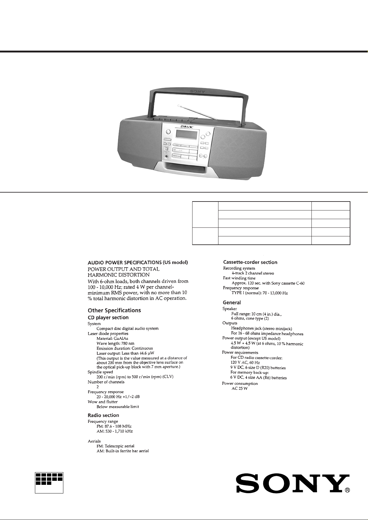
Sony CFDS-28 Service manual

CFD-S28
SERVICE MANUAL
Ver 1.0 1999. 03
CD
Section
TAPE
Section
US Model
E Model
Model Name Using Similar Mechanism NEW
CD Mechanism Type KSM-213CDM
Optical Pick-up Name KSS-213C
Model Name Using Similar Mechanism CFD-V10
Tape Transport Mechanism Type MF-V10-117
SPECIFICATIONS
– Continued on next page –
MICROFILM
CD RADIO CASSETTE-CORDER

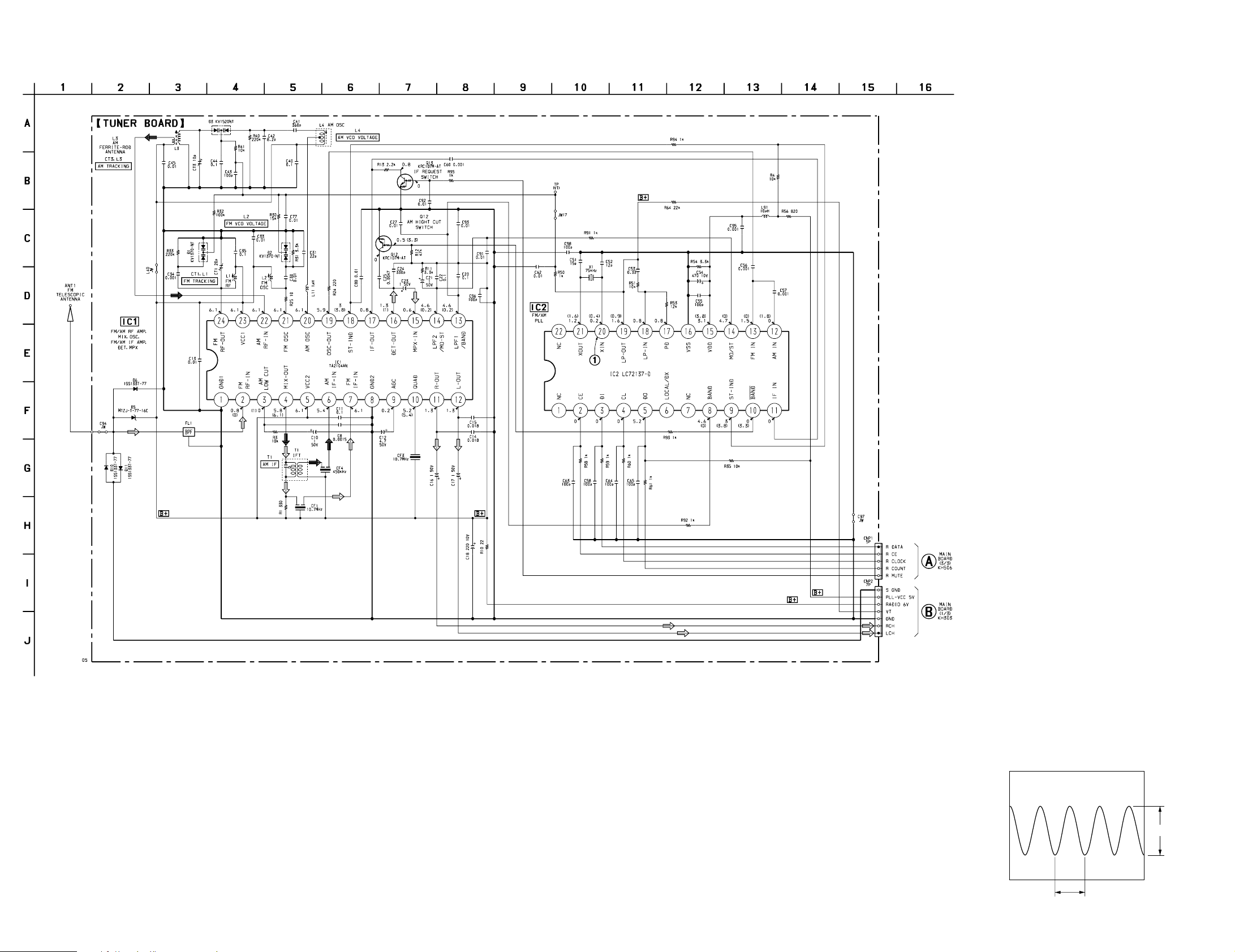
6-5. SCHEMATIC DIAGRAM – TUNER Section – • See page 45 for IC Block Diagrams.
Note on Schematic Diagram:
• All capacitors are in µF unless otherwise noted. pF: µµF
50 WV or less are not indicated except for electrolytics
and tantalums.
• All resistors are in Ω and 1/
specified.
¢
•
• U : B+ Line.
• H : adjustment for repair.
• Power voltage is dc 9 V and fed with regulated dc power
• Voltages and waveform are dc with respect to ground
• Voltages are tak en with a V OM (Input impedance 10 MΩ).
• Waveform is taken with a oscilloscope.
• Circled numbers refer to waveform.
• Signal path.
: internal component.
supply from battery terminal.
under no-signal (detuned) conditions.
no mark : FM
( ) : AM
Voltage variations may be noted due to normal production tolerances.
Voltage variations may be noted due to normal production tolerances.
F : FM
f : AM
4
W or less unless otherwise
(Page 37)
(Page 33π )
• Waveform
1 IC2 @º XIN (FM mode)
500 mV/DIV, 5 µs/DIV
1.8 Vp-p
– 27 –
13.3 µs
– 28 –

CFD-S28
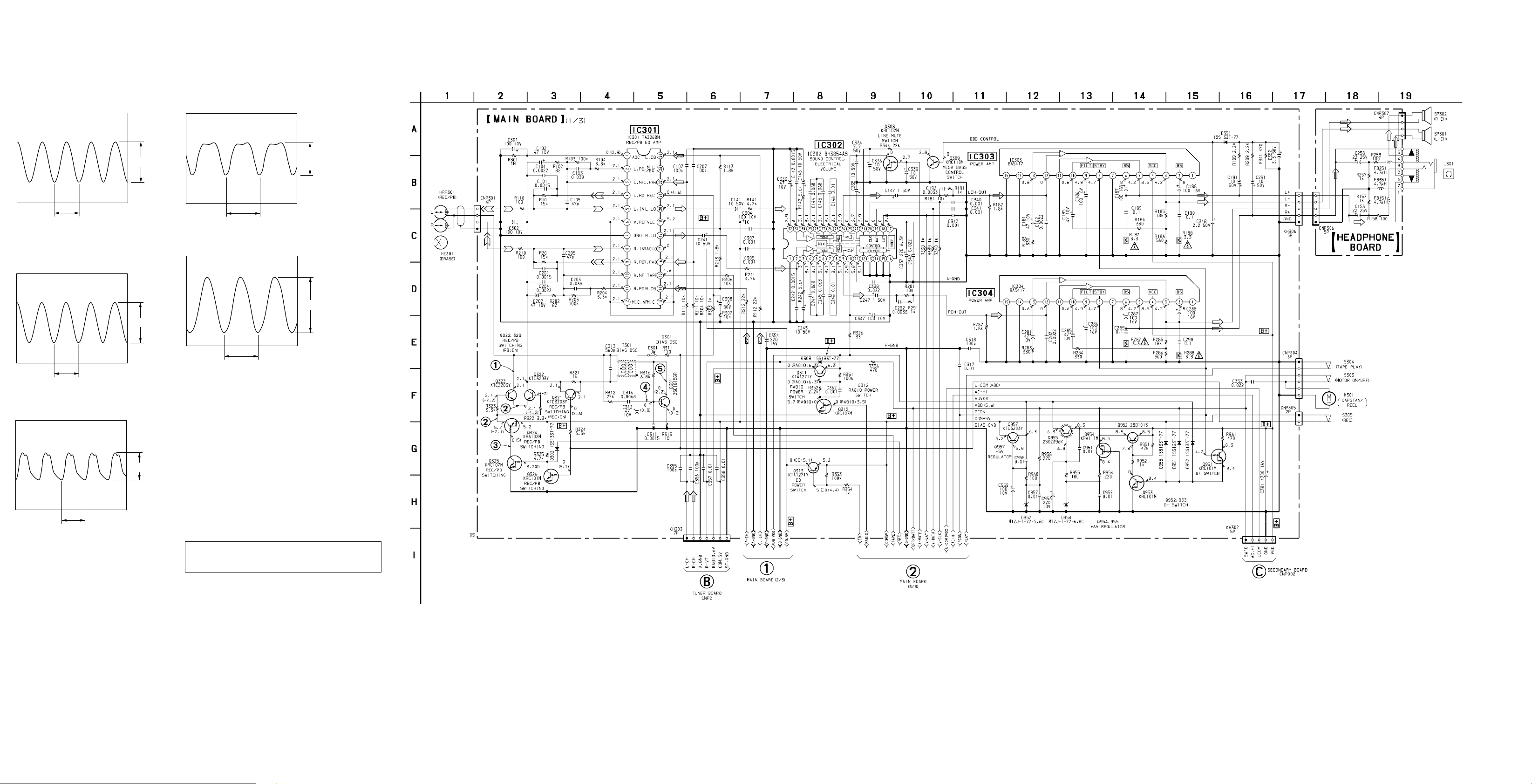
• Waveforms
– MAIN Board (1/3) –
1 Q323 Collector (REC mode)
20 V/DIV, 20 µs/DIV
20.8
µ
s
2 Q322 Emitter, Base
Q323 Emitter, Base
Q324 Collector (REC mode)
5 V/DIV, 20 µs/DIV
34.4 Vp-p
9.8 Vp-p
4 Q301 Base (REC mode)
500 mV/DIV, 10 µs/DIV
µ
s
20.8
5 Q301 Collector (REC mode)
1 V/DIV, 10 µs/DIV
6-7. SCHEMATIC DIAGRAM – MAIN Section (1/3) – • See page 45 for IC Block Diagrams.
1 Vp-p
3.6 Vp-p
20.8
µ
s
3 Q324 Base, Q325 Collector (REC mode)
50 mV/DIV, 10 µs/DIV
128 mVp-p
20.8 µs
20.8 µs
Note on Schematic Diagram:
• All capacitors are in µF unless otherwise noted. pF: µµF
50 WV or less are not indicated except for electrolytics
and tantalums.
• All resistors are in Ω and 1/
specified.
• 2 : nonflammable resistor.
• C : panel designation.
Note: The components identified by mark ! or dotted line
with mark ! are critical for safety.
Replace only with part number specified.
• U : B+ Line.
• Power voltage is dc 9 V and fed with regulated dc power
supply from battery terminal.
• Voltages and waveforms are dc with respect to ground
under no-signal conditions.
no mark : TAPE PLAY
( ) : TAPE REC
• Voltages are tak en with a V OM (Input impedance 10 MΩ).
Voltage variations may be noted due to normal production tolerances.
• Waveforms are taken with a oscilloscope.
Voltage variations may be noted due to normal production tolerances.
• Circled numbers refer to waveforms.
• Signal path.
F : TUNER (FM/AM)
E : T APE PLA Y
a : TAPE REC
J : CD PLAY
4
W or less unless otherwise
(Page 28)
(Page 36)
(Page 37)
(Page 44)
– 32 –
– 33 –
– 34 –
 Loading...