Sony CFD-S20CP Service Manual

CFD-S20CP
SERVICE MANUAL
Ver 1.3 2004.09
SUPPLEMENT-1
File this supplement with the service manual.
Subject: Change of CD Board
Change of CD Mechanism Block (KSM-213RDP→KSM-213CDP)
AEP Model
UK Model
E Model
(SPM-04041)
The CD board and CD mechanism block was changed from KSM-213RDP to
KSM-213CDP in the course of production.
This Supplement-1 only describes the change.
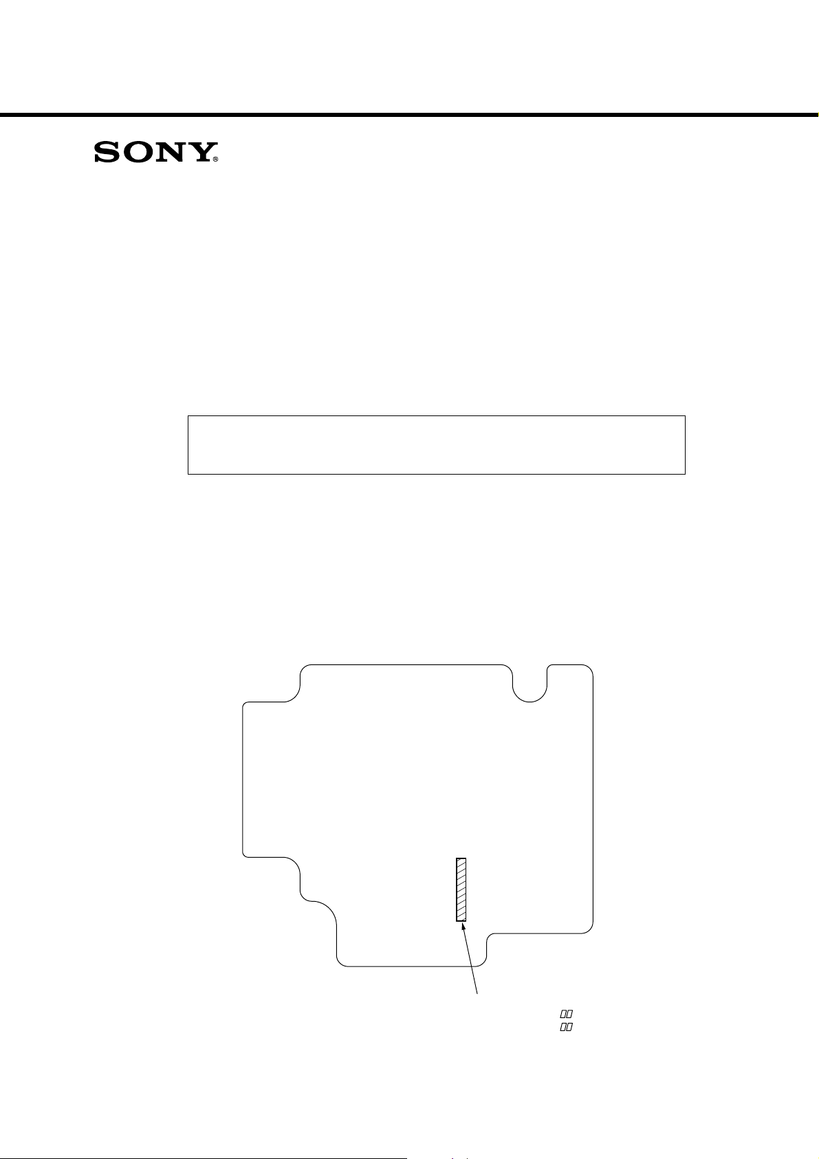
1. IDENTIFICATION
– CD BO
ARD (SIDE A) –
9-873-979-81
CD Board Part No.
Former type : 1-684-176New type : 1-687-530-

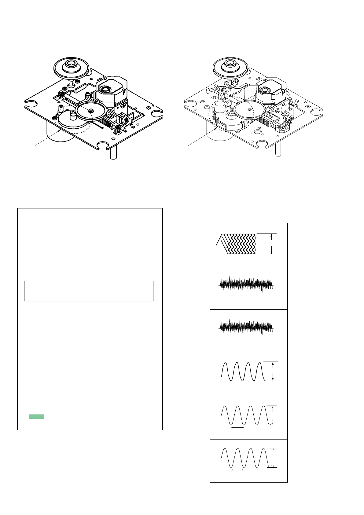
CFD-S20CP
KSM-213RDP
Without gear cover
THIS NOTE IS COMMON FOR PRINTED WIRING
BOARDS AND SCHEMATIC DIAGRAMS.
(In addition to this, the necessary note is
printed in each block.)
KSM-213CDP
With gear cover
• Wavef orms (Mode: PLAY)
— CD Board —
500mV/div 0.5µsec/div
1
Common Note on Schematic Diagrams:
• All capacitors are in µF unless otherwise noted. (p: pF)
50 WV or less are not indicated except for electrolytics
and tantalums.
• All resistors are in Ω and 1/
specified.
f
•
Note: The components identified by mark 0 or dotted line
• A : B+ Line.
•Total current is measured with no cassette installed.
•Power voltage is dc 9V and fed with regulated dc power
•Voltages are taken with a VOM (Input impedance 10 MΩ).
•Waveforms are taken with a oscilloscope.
• Circled numbers refer to waveforms.
• Signal path.
• (( )) : Refer to page of Service manual.
Common Note on Printed Wiring Boards:
• X : parts extracted from the component side.
• Y : parts extracted from the conductor side.
•
• : Pattern from the side which enables seeing.
• (( )) : Refer to page of Service manual.
: internal component.
with mark 0 are critical for safety.
Replace only with part number specified.
supply from battery terminal.
Voltage var iations may be noted due to normal produc-
tion tolerances.
Voltage var iations may be noted due to normal produc-
tion tolerances.
J : CD
f
: internal component.
4
W or less unless otherwise
0.85±0.2Vp-p
IC7014 (RF)
100mV/div 200µsec/div
2
Approx. 100mVp-p
IC701qd (FE)
100mV/div 200µsec/div
3
Approx. 100mVp-p
IC701qg (TE)
2V/div 0.05µsec/div
4
16.93MHz
IC701rk (XOUT)
2V/div 50nsec/div
5
60nsec
IC701 t; (FSX/16MIN (I))
2V/div 50nsec/div
6
1.8V
1.8V
6Vp-p
6Vp-p
7Vp-p
60nsec
IC1001 7 (CKIN (I))
2

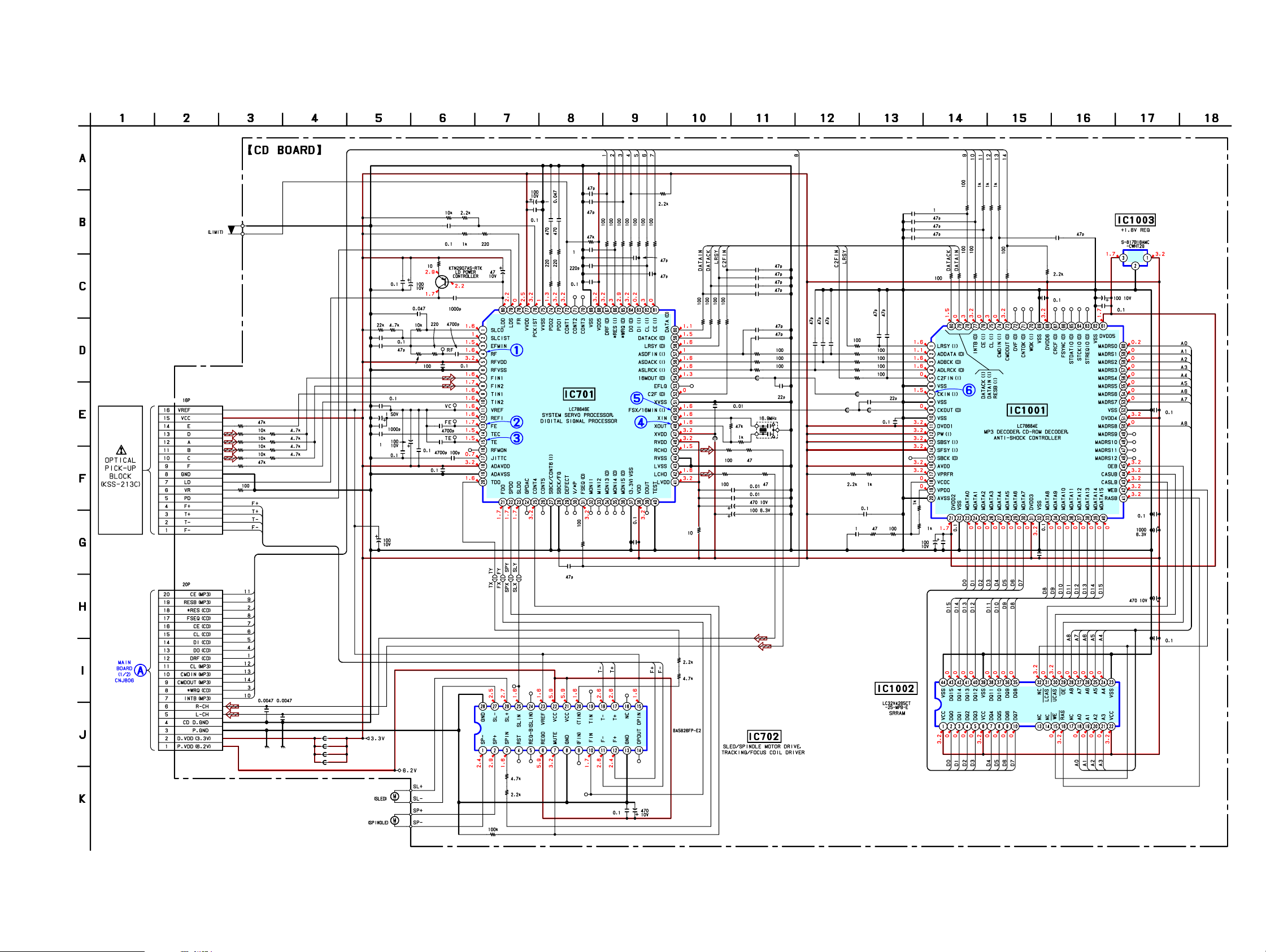
2. SCHEMATIC DIAGRAM — CD SECTION — • Refer to page 2 for Waveforms.
CFD-S20CP
CNP701
S701
R745
R701
R702
R703
R704
R705
R706
R755
R756
R757
R758
C701
C715
C718
C711
C712
C702
C703
C716
C707
C740
R759
C710
R708R710R709
C723
C721
C706
R707
R711
C717
R728 R727
C719
C713
C714
C705
C720
Q701
C743
R725
R763
C741
C750
C742
IC701
R740
C754
C753
R724
R716
R717
R718
R719
R720
C722
R721
R722
R731
C745
C751
R766
R723
FB701
R732
R733
C737
R714
R734
R715
R765
R713
C733
C732
C730
C729
R762
FB703
C760
C761
C762
C763
C764
C766
R735
R736
R737
X701
R761
C767
C1066
C1067
C1068
FB704
R1001
FB1001
C1012
R1002
R1003
R1004
R1005
R1081R1017
C1011
C1069
C1074
FB1002
C1010
C1070
R1018R1082
C1056
C1001
C1057
C1058
R1019
C1014
R1020
R1080
C1013
R1078
R1079
R1077
R1076
R1075
R1074
R1073
IC1001
C1044
C1037
R1068
C1059
IC1003
C1042
C1043
C1031
C1030
C1029
C709
C746
C744
R729R730C708
C704
R726
R764
((Page 28))
CNP702
C734 C731
FB702
FB705
FB706
FB707
•Voltage and waveforms are dc with respect to ground
under no-signal (detuned) conditions.
no mark : CD PLAY
M702
M701
R744
SL701
SL702
SL703
R743
R712
SL704
C756
C747
C1054
C1055
R760
R753
IC1002
IC702
C748
33
 Loading...