

Page 1

CFD-S20CP
SERVICE MANUAL
Ver 1.4 2004. 09
Section
Section
US Model
Canadian Model
Taiwan Model
Korean Model
Model Name Using Similar Mechanism CFD-S400/S500
CD
CD Mechanism Type KSM-213RDP
Optical Pick-up Name KSS-213R
Model Name Using Similar Mechanism CFD-S400/S500
TC
Tape Transport Mechanism T ype MF-S200
AUDIO POWER SPECIFICATIONS
POWER OUTPUT AND TOTAL
HARMONIC DISTORTION
With 3.2-ohm loads, both channels driven from
150 - 6,300 Hz; rated 1.8 W per channelminimum RMS power, with no more than 10%
total harmonic distortion in AC operation.
Other Specifications
CD player section
System
Compact disc digital audio system
Laser diode properties
Material: GaAlAs
Wave length: 780 nm
Emission duration: Continuous
Laser output: Less than 44.6 µW
(This output is the value measured at a distance of
about 200 mm from the objective lens surface on
the optical pick-up block with 7 mm aperture.)
Spindle speed
200 r/min (rpm) to 500 r/min (rpm) (CLV)
Number of channels
2
Frequency response
20 - 20,000 Hz +1/–2 dB
Wow and flutter
Below measurable limit
SPECIFICATIONS
Radio section
Frequency range
FM: 87.5 - 108 MHz
AM: 530 - 1,710 kHz (US, CND)
AM: 531 - 1,611 kHz (KR, TW)
Antennas
FM: Telescopic antenna
AM: Built-in ferrite bar antenna
Cassette-corder section
Recording system
4-track 2 channel stereo
Fast winding time
Approx. 120 sec. with Sony cassette C-60
Frequency response
TYPE I (normal): 80 - 10,000 Hz
– Continued on next page –
9-873-978-05
2004I04-1
© 2004. 09
CD RADIO CASSETTE-CORDER
Sony Corporation
Personal Audio Company
Published by Sony Engineering Corporation
1
Page 2

CFD-S20CP
Ver 1.3
General
Speaker
Full range: 10 cm (4 in.) dia.,
3.2 ohms, cone type (2)
Outputs
Headphones jack (stereo minijack)
For 16 - 68 ohms impedance headphones
Power output
2.3 W + 2.3 W (at 3.2 ohms, 10%
harmonic distortion)
Power requirements
For CD radio cassette-corder:
US, CND, TW model:
120 V AC, 60 Hz
KR model:
220 V AC, 60 Hz
9 V DC, 6 size D (R20) batteries
For remote control:
3 V DC, 2 size AA (R6) batteries
Battery life
For CD radio cassette-corder:
FM recording
Sony R20P: approx. 13.5 h
Sony alkaline LR20: approx. 20 h
Tape playback
Sony R20P: approx. 7.5 h
Sony alkaline LR20: approx. 15 h
CD playback
Sony R20P: approx. 2.5 h
Sony alkaline LR20: approx. 7 h
Dimensions
Approx. 386 × 166 × 252 mm (w/h/d)
1/4 × 6 5/8 × 10 inches) (incl. projecting parts)
(15
Mass
Approx. 3.3 kg (7 lb. 4 oz.) (incl. batteries)
Supplied accessories
AC power cord (1)
Remote control (RMT-CS20CPA) (1)
Design and specifications are subject to change without
notice.
•Abbreviation
CND : Canadian model
KR : Korean model
TW : Taiw an model
CAUTION
Use of controls or adjustments or performance of procedures other than those specified herein may result in hazardous radiation exposure.
Flexible Circuit Board Repairing
• Keep the temperature of the soldering iron around 270˚C during
repairing.
• Do not touch the soldering iron on the same conductor of the
circuit board (within 3 times).
• Be careful not to apply force on the conductor when soldering
or unsoldering.
Notes on Chip Component Replacement
• Never reuse a disconnected chip component.
• Notice that the minus side of a tantalum capacitor may be dam-
aged by heat.
NOTES ON HANDLING THE OPTICAL PICK-UP BLOCK
OR BASE UNIT
The laser diode in the optical pick-up block may suffer electrostatic
breakdown because of the potential difference generated by the
charged electrostatic load, etc. on clothing and the human body.
During repair, pay attention to electrostatic breakdown and also use
the procedure in the printed matter which is included in the repair
parts.
The flexible board is easily damaged and should be handled with
care.
NOTES ON LASER DIODE EMISSION CHECK
The laser beam on this model is concentrated so as to be focused on
the disc reflective surface by the objective lens in the optical pickup block. Therefore, when checking the laser diode emission,
observe from more than 30 cm away from the objective lens.
SAFETY-RELATED COMPONENT WARNING!!
COMPONENTS IDENTIFIED BY MARK 0 OR DOTTED LINE
WITH MARK 0 ON THE SCHEMATIC DIAGRAMS AND IN
THE PARTS LIST ARE CRITICAL TO SAFE OPERATION.
REPLACE THESE COMPONENTS WITH SONY PARTS WHOSE
PART NUMBERS APPEAR AS SHOWN IN THIS MANUAL OR
IN SUPPLEMENTS PUBLISHED BY SONY.
ATTENTION AU COMPOSANT AYANT RAPPORT
À LA SÉCURITÉ!!
LES COMPOSANTS IDENTIFIÉS P AR UNE MARQUE 0 SUR LES
DIAGRAMMES SCHÉMA TIQUES ET LA LISTE DES PIÈCES SONT
CRITIQUES POUR LA SÉCURITÉ DE FONCTIONNEMENT. NE
REMPLACER CES COMPOSANTS QUE PAR DES PIÈCES SONY
DONT LES NUMÉROS SONT DONNÉS DANS CE MANUEL OU
DANS LES SUPPLÉMENTS PUBLIÉS PAR SONY.
2
Page 3

TABLE OF CONTENTS
1. SERVICING NOTES......................................................... 4
2. GENERAL............................................................................ 5
3. DISASSEMBLY
3-1. Cabinet Top Assy ................................................................ 7
3-2. Cabinet Front Assy, Cabinet Rear Assy ..............................7
3-3. Wires ................................................................................... 8
3-4. MD Block............................................................................8
3-5. Cassette Door Assy ............................................................. 9
3-6. LCD Board, Control (4) Board ...........................................9
3-7. Main Board ....................................................................... 10
3-8. Tuner Board....................................................................... 10
3-9. Power Board......................................................................11
3-10. CD Lid............................................................................... 11
3-11. CD Block Assy.................................................................. 12
3-12. Optical Pick-up ................................................................. 12
3-13. R/P Head (HRP301), TC Board ........................................ 13
3-14. Motor Assy (M801), Main Belt (B), Sub Belt (B) ............ 13
CFD-S20CP
4. MECHANICAL ADJUSTMENTS............................... 14
5. ELECTRICAL ADJUSTMENTS
Tape Section .......................................................................... 14
Tuner Section......................................................................... 15
CD Section ............................................................................ 16
6. DIAGRAMS
6-1. IC Pin Descriptions ........................................................... 17
6-2. Circuit Boards Location .................................................... 19
6-3. Block Diagram – CD Section –......................................... 20
6-4. Block Diagram – Main Section –......................................21
6-5. Printed Wiring Board – CD Section – ...............................22
6-6. Schematic Diagram – CD Section –.................................. 24
6-7. Printed Wiring Board – Tuner Section – ...........................25
6-8. Schematic Diagram – Tuner Section –.............................. 26
6-9. Printed Wiring Boards – Main Section – .......................... 27
6-10. Schematic Diagram – Main Section (1/2) – ...................... 28
6-11. Schematic Diagram – Main Section (2/2) – ...................... 29
6-12. Printed Wiring Board – TC Section – ...............................30
6-13. Schematic Diagram – TC Section – .................................. 31
6-14. Printed Wiring Boards – Control Section –....................... 32
6-15. Schematic Diagram – Control Section – ........................... 33
6-16. Printed Wiring Boards – Display Section – ...................... 34
6-17. Schematic Diagram – Display Section –........................... 35
6-18. Printed Wiring Boards – Power Supply Section – ............36
6-19. Schematic Diagram – Power Supply Section –................. 37
6-20. IC Block Diagrams............................................................ 38
7. EXPLODED VIEWS
7-1. Main Section ..................................................................... 40
7-2. Cabinet Front Section........................................................ 41
7-3. Cabinet Top Section .......................................................... 42
7-4. Cabinet Rear Section.........................................................43
7-5. Tape Mechanism Section .................................................. 44
7-6. CD Mechanism Section .................................................... 45
8. ELECTRICAL PARTS LIST.........................................46
3
Page 4
CFD-S20CP
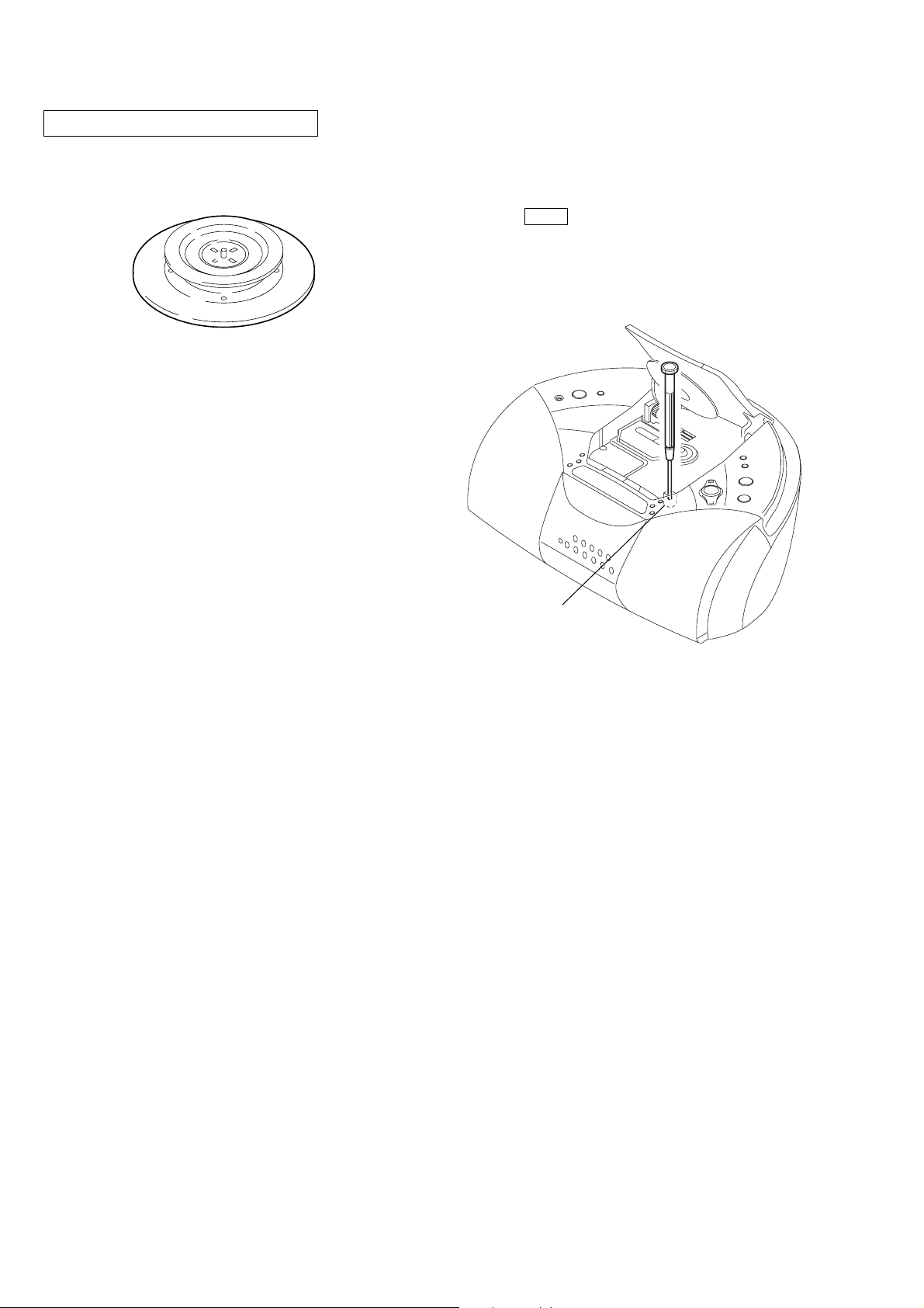
SECTION 1
SERVICING NOTES
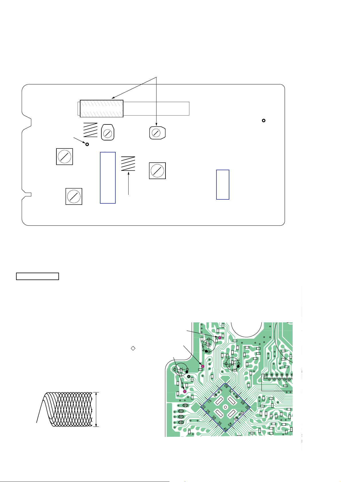
CHUCK PLATE JIG ON REPAIRING
On repairing CD section, playing a disc without the lid (CD), use
Chuck Plate Jig.
• Code number of Chuck Plate Jig: X-4918-255-1
LASER DIODE AND FOCUS SEARCH OPERATION
CHECK
1. Turn ON the [POWER] button and press [CD] button to
CD position.
2. Open the CD lid.
3. Turn on S801 with screwdriver, etc. as following figure.
4. Press the N X (CD) button.
5. Confirm the laser diode emission while observing the objecting
lens. When there is no emission, Auto P ower Control circuit or
Optical Pick-up is broken.
Objective lens moves up and do wn three times for focus search.
S801
4
Page 5
SECTION 2
Location of controls
Loading a CD
With the labeled side up
Inserting a cassette
With the side you want
to play facing you
Total track number Programmed track Playing orderTotal playing time
Display
CD
MEGA BASS
Z PUSH
OPEN/CLOSE
VOL +*, –
., >
TUNE –, +
DISPLAY
ENT
MEMORY
MODE
REPEAT
i
Number buttons
x
u*
POWER
SLEEP
OPR/BATT
RADIO BAND
AUTO PRESET
TAPE
Display
Remote sensor
MP3 FOLDER –FOLDER +
SOUND
*The button has a tactile dot.
*
GENERAL
CFD-S20CP
5
Page 6
CFD-S20CP
SECTION 3
DISASSEMBLY
• The equipment can be removed using the following procedure.
SET
3-1. CABINET T OP ASSY
(Page 7)
3-2. CABINET FRONT ASSY,
CABINET REAR ASSY
(Page 7)
3-3. WIRES
(Page 8)
3-4. MD BLOCK
(Page 8)
3-5. CASSETTE DOOR ASSY
(Page 9)
3-6. LCD BOARD,
CONTROL (4) BOARD
(Page 9)
3-7. MAIN BOARD
(Page 10)
3-10. CD LID
(Page 11)
3-8. TUNER BOARD
3-13. R/P HEAD (HRP301),
TC BOARD
(Page 13)
3-11. CD BLOCK ASSY
3-12. OPTICAL PICK-UP
(Page 10)
(Page 12)
(Page 12)
3-9. POWER BOARD
(Page 11)
3-14. MOTOR ASSY (M801),
MAIN BELT (B),
SUB BELT (B)
(Page 13)
6
Page 7
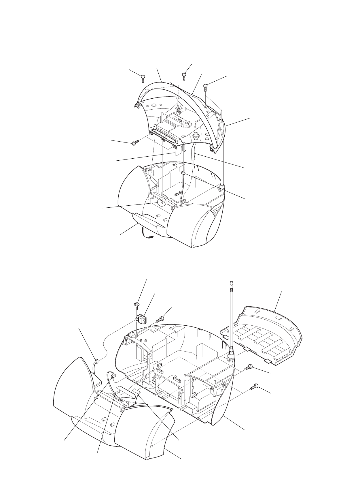
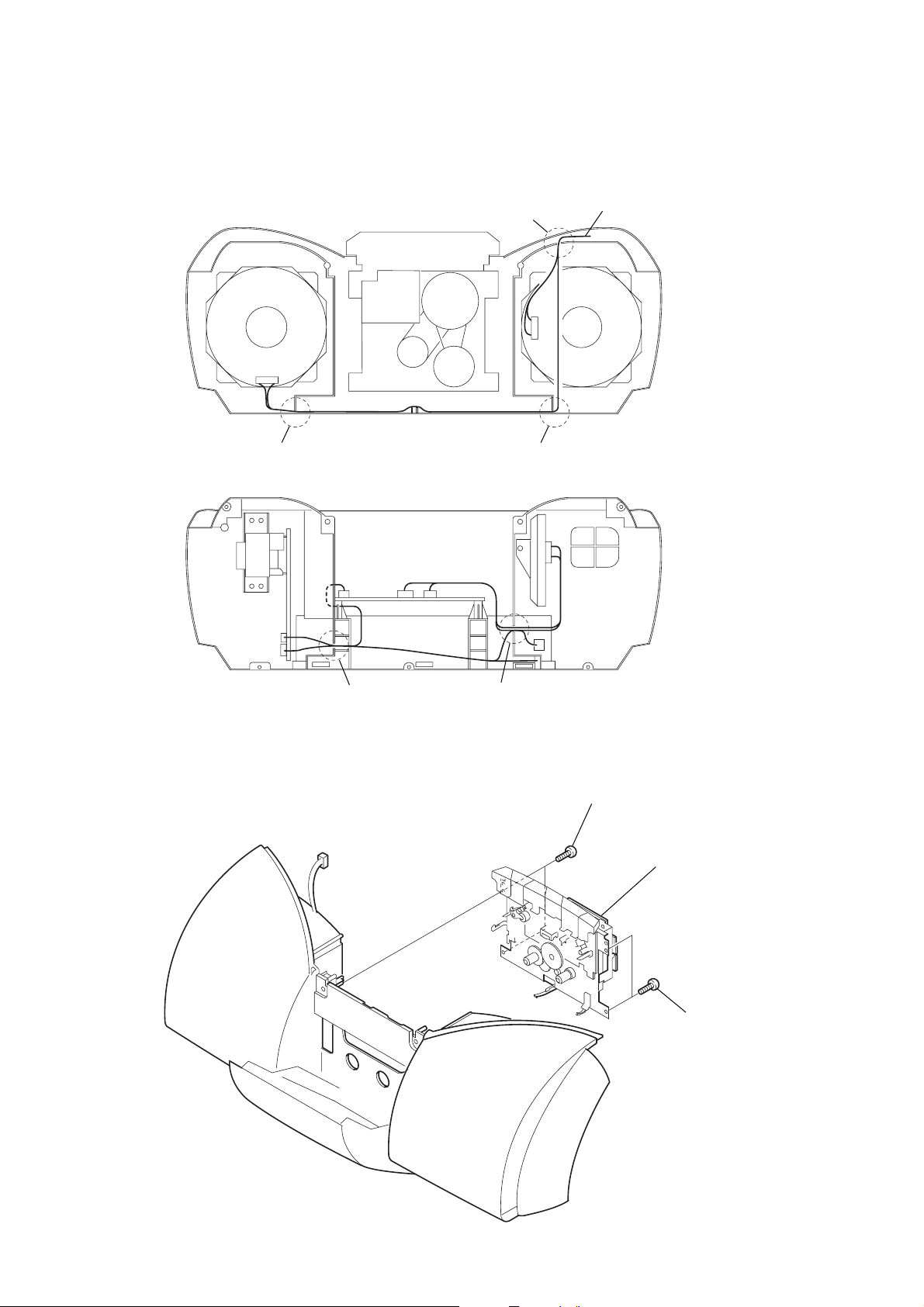
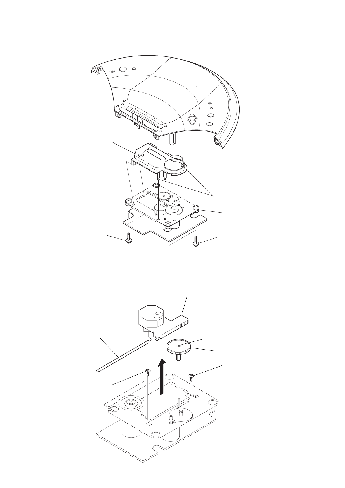
Note : Follow the disassembly procedure in the numerical order given.
3-1. CABINET TOP ASSY
2
1
BTP 2.6x6
6
3
screw (2.6)
CNJ806
handle
screw (2.6)
CD lid
4
screw (2.6)
8
cabinet top assy
5
CNJ804
CFD-S20CP
claw
cassette door assy
3-2. CABINET FRONT ASSY, CABINET REAR ASSY
1
PWH 2.6x10
2
HEADPHONE board
7
3
CNP323
screw (2.6)
7
connector
(S801)
9
battery lid
4
CNP801
5
CNJ807
6
CNJ805
qa
cabinet front assy
8
0
qs
cabinet rear assy
screw (2.6)
screw (2.6)
7
Page 8
CFD-S20CP
3-3. WIRES
Put flat cable and wires between the cabinets and push them in the
grooves located at A to E in the figure to prevent disconnection
before assembling the set.
C
from HEADPHONE board
cabinet front
3-4. MD BLOCK
A
D
B
cabinet rear
E
1
BVTP 2.6x10
3
MD block
2
BVTP 2.6x10
8
Page 9
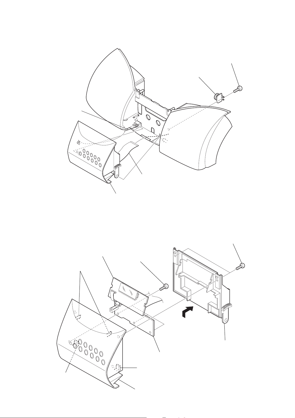
3-5. CASSETTE DOOR ASSY
0
cassette spring
2
damper
1
BVTP 2.6x1
CFD-S20CP
3
cassette door assy
3-6. LCD BOARD, CONTROL (4) BOARD
6
LCD board
5
claws
flexible flat cable
4
BVTP 2.6x10
2
1
BVTP (2.6)
claw
CONTROL (4) board
7
claw
cassette door sub assy
3
cassette holder
9
Page 10
CFD-S20CP
8
3-7. MAIN BOARD
1
PWH 2.6x10
2
HEADPHONE board
3
CNP322
4
CNP902
7
MAIN board
6
BVTP 2.6x10
3-8. TUNER BOARD
5
CNP1
2
telescopic antenna
1
B 3x
10
4
BVTP 2.6x10
5
claws
6
3
CNP1
7
TUNER board
Page 11
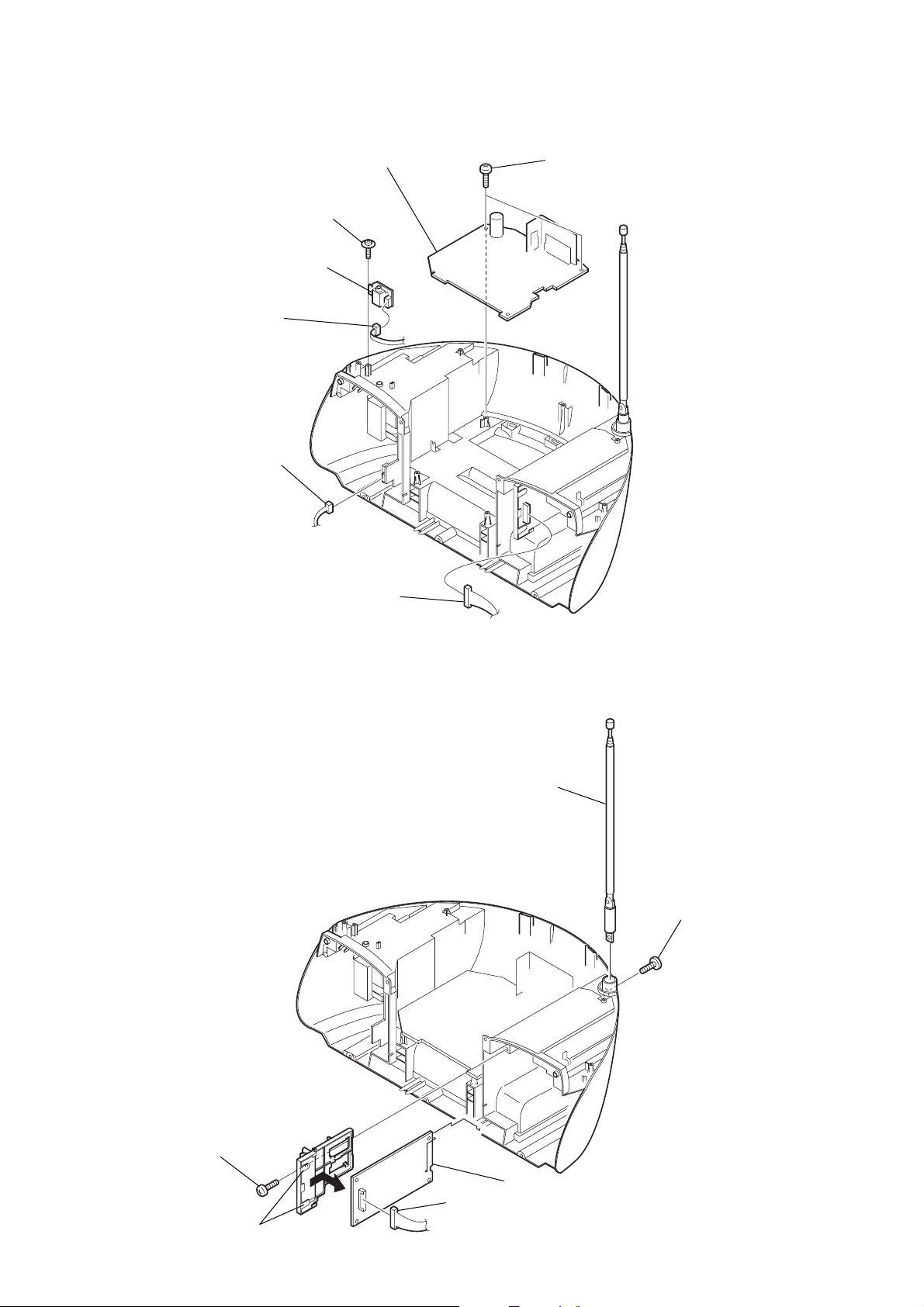
3-9. POWER BO ARD
3
BVTP 2.6x10
4
BVTP 2.6x10
CFD-S20CP
3-10. CD LID
2
CNP901
1
CNP902
3
5
BVTP 2.6x10
CD lid
6
POWER board
2
claw
1
CD spring
claw
11
Page 12
CFD-S20CP
y
)
3-11. CD BLOCK ASSY
3
CD cover
2
3-12. OPTICAL PICK-UP
PWH 2.6x10
5
sled shaft
4
6
optical pick-up
claws
claw
1
4
CD block ass
1
PWH 2.6x10
gear (A)
2
PWB tapping (M2
12
3
PWB tapping (M2)
Page 13
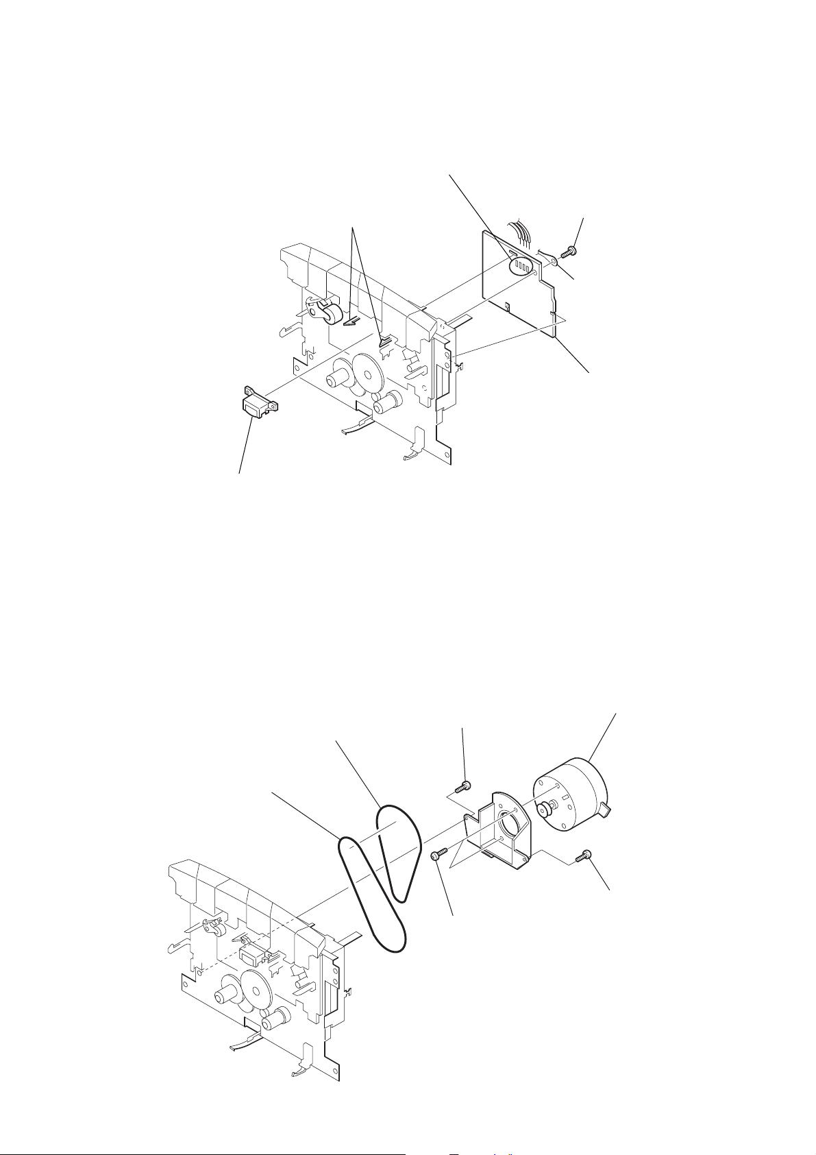
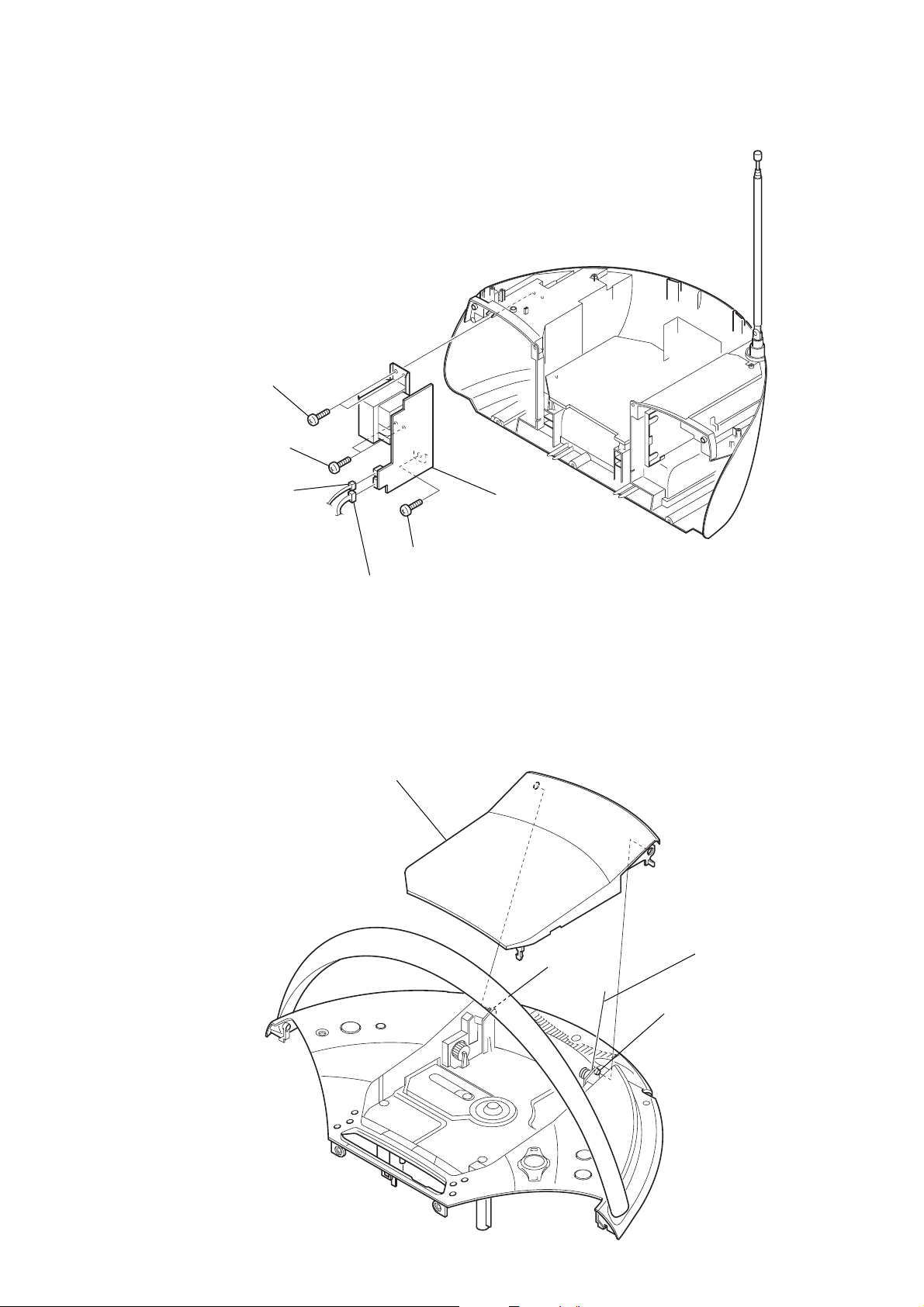
3-13. R/P HEAD (HRP301), TC BOARD
)
claws
4
Removal the solders.
2
BVTP 2x4
lug
3
TC board
CFD-S20CP
1
R/P head (HRP301)
3-14. MOTOR ASSY (M801), MAIN BELT (B), SUB BELT (B)
3
main belt (B)
4
sub belt (B)
2
bind DT M2x6
6
motor assy (M801
5
pan M2.6x4.5
1
bind DT M2x6
13
Page 14
CFD-S20CP
SECTION 4
MECHANICAL ADJUSTMENTS
SECTION 5
ELECTRICAL ADJUSTMENTS
PRECAUTION
1. Clean the following parts with a denatured-alcohol-moistened
swab :
record/playback head pinch roller
erase head rubber belts
capstan idlers
2. Demagnetize the record/playback head with a head demagnetizer. (Do not bring the head magnetizer close to the erase head.)
3. Do not use a magnetized screwdriver for the adjustments.
4. The adjustments should be performed with the rated power
supply voltage (9V) unless otherwise noted.
Torque Measurement
Mode Torque meter Meter reading
2.95 – 6.86 mN • m
FWD CQ-102C (30 – 70 g • cm)
(0.42 – 0.97 oz • inch)
FWD
Back Tension
FF CQ-201B (more than 60 g • cm)
REW CQ-201B (more than 60 g • cm)
CQ-102C (1.5 – 5.5 g • cm)
0.15 – 0.53 mN • m
(0.021 – 0.076 oz • inch)
more than 5.88 mN • m
(more than 0.83 oz • inch)
more than 5.88 mN • m
(more than 0.83 oz • inch)
TAPE SECTION 0 dB = 0.775 V
• Standard Output Level
Output terminal HP OUT
load impedance 32 Ω
output signal level 0.25 V (–10 dB)
• Test T ape
Type Signal Used for
WS-48A 3 kHz, 0 dB tape speed adjustment
Tape Speed Adjustment
Procedure:
Mode: playback
test tape
WS-48A
(3 kHz, 0 dB)
set
i
jack (J321)
Adjust so that the value on the digital frequency counter is
3,000 Hz.
digital frequency
counter
32
Ω
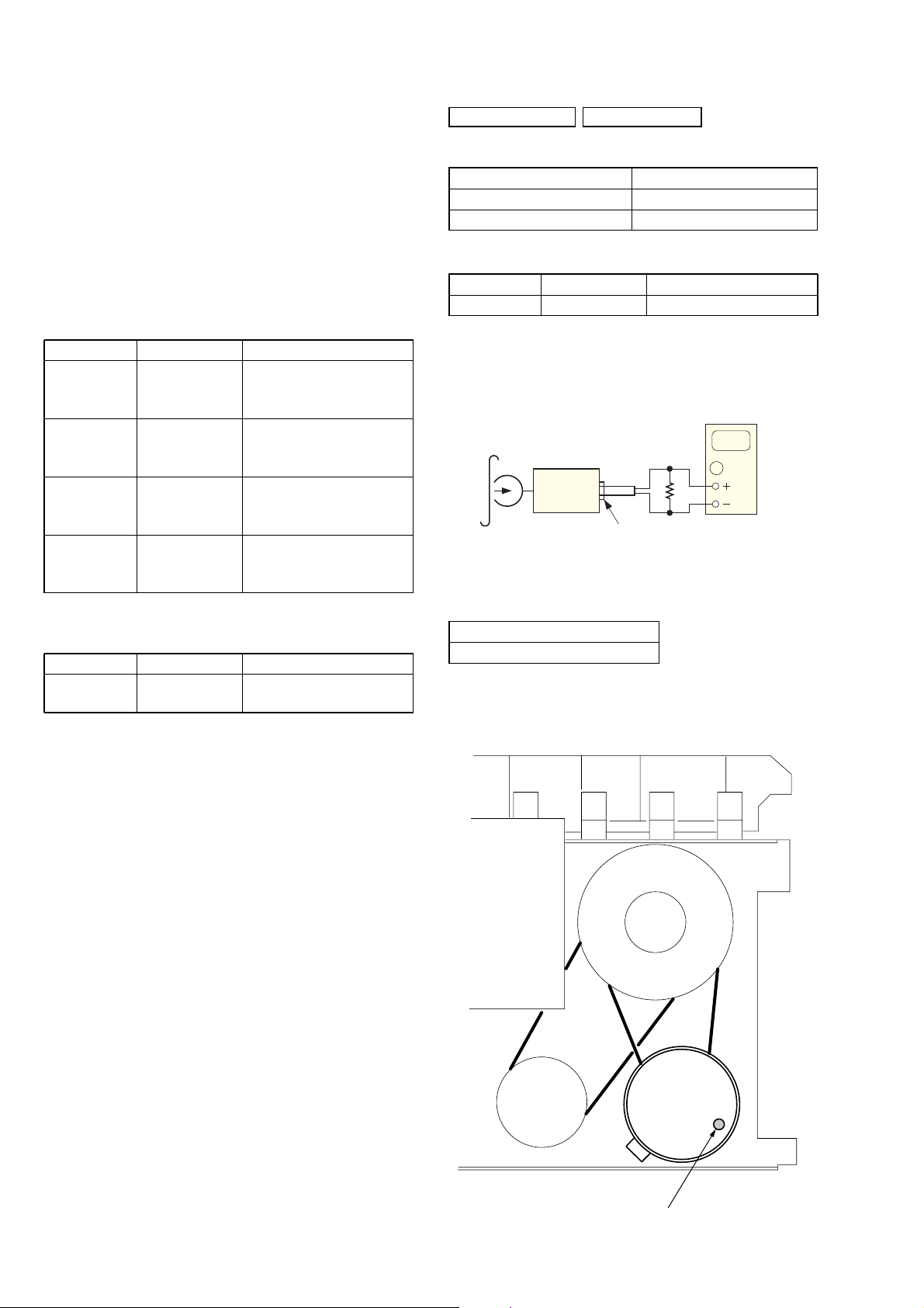
Tape Tension Measurement
Mode Tension meter Meter Reading
FWD CQ-403A
more than 100 g
(more than 3.53 oz)
Specification Value:
Digital frequency counter
2,940 to 3,060 Hz
Adjust so that the frequency at the beginning and that at the end of
tape winding are between 2,970 to 3,030 Hz.
Adjustment Location:
14
Tape speed adjustment
control inside motor
Page 15
CFD-S20CP
)
Ver 1.2
TUNER SECTION 0 dB = 1 µV
• FM Section
Setting:
RADIO BAND•AUTO PRESET button: FM
FM RF signal
generator
TP (FM IN)
0.01
µ
F
75 kHz frequency
deviation by 1 kHz signal
output level : as low as possible
• AM Section
Setting:
RADIO BAND•AUTO PRESET button: AM
AM RF signal
generator
30% amplitude
modulation by
400 Hz signal
• Connecting Level Meter (FM and AM)
set
Put the lead-wire
antenna close to
the set.
level meter
(range: 0.5–5 V ac
32 Ω
set
FM IF ADJUSTMENT
Adjust for a maximum reading on level meter.
T2
10.7 MHz
FM FREQUENCY COVERAGE
ADJUSTMENT
Frequency Display 87.5 MHz 108 MHz
Reading on Digital voltmeter 1.3 ± 0.3 V 3.0 ± 0.2 V
Adjustment Part <confirmation> L2
FM TRACKING ADJUSTMENT
Adjust for a maximum reading on level meter.
L1 CT1
87.5 MHz 108 MHz
AM IF ADJUSTMENT
Adjust for a maximum reading on level meter.
T1
450 kHz
AM FREQUENCY COVERAGE
ADJUSTMENT
Frequency Display 531 kHz 1,611 kHz
Reading on Digital voltmeter 1.0 ± 0.05 V 5.3 ± 0.7 V
Adjustment Part L4 <confirmation>
AM TRACKING ADJUSTMENT
Adjust for a maximum reading on level meter.
L3 CT3
621 kHz 1,404 kHz
i jack (J321)
• Connecting Digital Voltmeter (FM and AM)
digital
voltmeter
100 kΩ
TP (VT)
•Repeat the procedures in each adjustment several times, and the
frequency coverage and tracking adjustments should be finally
done by the trimmer capacitors.
Adjustment Location: See page 16.
15
Page 16
CFD-S20CP
7
0
0
Adjustment Location:
– MAIN board (component side) –
TP (FM IN)
(CONDUCTOR SIDE)
T1
AM
IF
ADJUSTMENT
ADJUSTMENT
T2
FM
IF
T1
T2
L1
L3
CT1
IC1
CT1, L1
FM
TRACKING
ADJUSTMENT
L2
L2
FM
FREQUENCY
COVERAGE
ADJUSTMENT
CT3, L3
AM
TRACKING
ADJUSTMENT
CT3
L4
TP (VT)
(CONDUCTOR SIDE)
L4
AM
FREQUENCY
COVERAGE
ADJUSTMENT
IC2
CD SECTION
CD section adjustments are done automatically in this set.
In case of operation check, confirm that focus bias.
FOCUS BIAS CHECK
1. Connect the oscilloscope between IC701 pin 4 and pin qa (or
TP (RF) and TP (VREF)).
2. Insert the disc (YEDS-18). (Part No. : 3-702-101-01)
3. Press the N X (CD) button.
4. Confirm that the oscilloscope waveform is as shown in the
figure below. (eye pattern)
A good eye pattern means that the diamond shape ( ) in the
center of the waveform can be clearly distinguished.
• RF signal reference waveform (eye pattern)
VOLT/DIV : 50 mV (10 : 1 probe in use)
TIME/DIV : 500 nS
RF level :
0.85 ± 0.2 Vp-p
When observing the eye pattern, set the oscilloscope for AC range
and raise vertical sensitivity.
TP
C719
C706
C717
(VREF)
C701
C721
R709
C711
C712
C740
TP
C722
R707
C714
C707
R759
C713
C709
R710
TP(RF)
R729
IC701
Test Point:
– CD board (conductor side) –
TP
(RF)
TP
(VREF)
TP
(TE)
C715
(FE)
C716
C718
TP
(TE)
C720
TX
TY
FX
FY
SPX
SPY
SLX
SLY
R740
C756
R708
R711
R730
Q701
C732
C705
C710
R727
C746
C733
C737
C708
R728
R765
R726
R764
R724
C742
FB704
R725
R763
C744
C743
C762
R732
FB703
C767
R733
R737
CNP701
C763
C761
R735
C766
C760
R734
R723
C764
R745
R757
R755
C1068
R736
R706
R1001
FB1001
C1066
C1074
R704
R1002
R1003
C1069
C1067
C1
R1
FB1002
R702
C
R1004
16
Page 17
CFD-S20CP
SECTION 6
DIAGRAMS
6-1. IC PIN DESCRIPTIONS
• IC1001 LC78683E-US-E (MP3 DECODER, CD-ROM DECODER, ANTI-SHOCK CONTROLLER) (CD BOARD)
Pin No. Pin Name I/O Pin Description
1 LRSY I CD L/R clock input
2 ADDATA O Audio data output
3 ADBCK O Audio bit clock output
4 ADLRCK O Audio L/R clock output
5 C2FIN I CD C2 error flag input
6 VSS — Ground
7 CKIN I System clock (16.9344 MHz) input
8 VSS — Ground
9CKOUT O Clock (384Fs) output for external DF/DAC.
10 VSS — Ground
11 DVDD1 — Digital power supply pin for I/O.
12 PW I CD subcode data serial input
13 SBSY I CD subcode block synchronized signal input
14 SFSY I CD subcode frame synchronized signal input
15 SBCK O Serial clock output for CD subcode transfer. (Not used. (Open))
16 AVDD — Analog (PLL) power supply pin
17 VPRFR — VCO oscillation range setting pin
18 VCOC I VCO control voltage input
19 VPDO O VCO charge pump output
20 AVSS — Analog ground
21 DVDD2 — Power supply pin for internal logic.
22 VSS — Ground
23 to 30 MDATA0 to 7 I/O DRAM data bus 0 to 7
31 DVDD3 — Digital power supply pin for I/O.
32 VSS — Ground
33 to 40 MDATA8 to 15 I/O DRAM data bus 8 to 15
41 RASB O Row Address Strobe signal output (L: active)
42 WEB O Data Write Enable signal output (L: active)
43 CASLB O Column Address Strobe signal output (for lower byte, L: active)
44 CASUB O Column Address Strobe signal output (for upper byte, L: active)
45 OEB O Output enable signal output (L: active)
46 to 49 MADRS12 to 9 O DRAM address output 12 to 9 (Not used. (Open))
50 MADRS8 O DRAM address output 8
51 DVDD4 — Digital power supply pin for I/O.
52 VSS — Ground
53 to 60 MADRS7 to 0 O DRAM address output 7 to 0
61 DVDD5 — Power supply pin for internal logic.
62 VSS — Ground
63 STREQ I/O
64 STCK I/O MP3 data transfer clock input/DRAM data transfer clock output (Not used. (Open))
65 STDAT I/O MP3 data serial input/DRAM data serial output (Not used. (Open))
66 FSYNC O MP3 frame synchronized signal input (H: active) (Not used. (Open))
67 CRCF O
68 DVDD6 — Power supply pin for internal logic.
69 VSS — Ground
70 WOK I
MP3 data request flag output (H: active)/DRAM data request flag input (H: active)
(Not used. (Open))
CDROM-CRC flag output (H: active)/DRAM data output enable signal output
(H: active) (Not used. (Open))
DRAM write OK input (at CD-DA, H: active)/DRAM data request flag input
(at CD-ROM, H: active)
17
Page 18

CFD-S20CP
Pin No. Pin Name I/O Pin Description
71 CNTOK O
72 OVF O
73 CMDOUT O Command serial data output (Nch open drain output pin)
74 CMDIN I Command serial data input
75 CL I Command serial clock input
76 CE I Command enable input (H: active)
77 INTB O Interrupt signal output (L: active)
78 RESB I System reset input (L: active)
79 DATAIN I CD serial data input
80 DATACK I CD bit clock input
Data connecting point detection completion flag output (at CD-DA, H: active)/DRAM
data serial output (at CD-ROM, H: active) (Not used. (Open))
DRAM write discontinue flag output (at CD-DA, H: active)/DRAM data transfer
clock output (at CD-ROM, H: active) (Not used. (Open))
18
Page 19
• IC801 µPD784216AGF-527-3BA (SYSTEM CONTROLLER) (MAIN BOARD)
d
Pin No. Pin Name I/O Pin Description
1 TU-CE O PLL chip enable output
2 TU-DATA O PLL serial data output
3 TU-CLK O PLL serial data transfer clock output
4 TU-COUNT I PLL serial count data input
5 TU-MUTE O Tuner muting ON/OFF control signal output (L: muting ON)
6 DEST1 I Destination setting input (Fixed at L: US, Canadian model, H: Singapore, Korean model)
7 DEST2 I Destination setting input (Fixed at L: US, Canadian model, H: Singapore, Korean model)
8 TEST-B O Fixed at L in this set.
9 VDD — Power supply pin (+3.3 V)
10 TEST-A I Fixed at L in this set.
11 EEPROM-SCL O Serial clock output for EEPROM IC (IC802).
12 EEPROM-SDA I/O Serial data bus input from/output for EEPROM IC (IC802).
13 to 16 N.C — Not used. (Open)
17, 18 ISS1, 2 O ISS1, 2 output
19 TU-ON O Tuner power ON/OFF control signal output (L: power ON)
20 TAPE-ON O Tape power ON/OFF control signal output (L: power ON)
21 CD-ON O CD power ON/OFF control signal output (L: power ON)
22 TEST/VPP I Fixed at L.
23 to 27 N.C — Not used. (Open)
28 MP3-LED O MP3 LED drive signal output (L: active)
29 LCD-RST O LCD system reset signal output (L: reset)
30 LCD-C/D O LCD command data output
31 LCD-CS O LCD chip select data output
32 LCD-DATA O LCD serial data output
33 LCD-CLK O LCD clock output
34 N.C — Not used. (Open)
35 FM/AM SHIFT O Shift point output for oscillation frequency change.
36 N.C — Not used. (Open)
37 VDD — Power supply pin (+3.3 V)
38 X2 O System clock output (5 MHz)
39 X1 I System clock input (5 MHz)
40 VSS — Ground
41 XT2 O Sub clock output (Not used. (Open))
42 XT1 I Sub clock input (Not used. (Connect to VSS))
43 RESET I System reset signal input (L: reset)
44 AC-CHK I AC power supply detection signal input (L: AC in)
45 RMC IN I Sircs receiver data input
46 WAKE-UP I Wake-up input
47 N.C — Not used. (Open)
48 CD-DOOR I CD lid open/close detection switch input (L: close)
49 INTB (MP3) I Interrupt request signal input (L: active)
50 WRQ (CD) I CD interruption signal input
51 AVDD — Power supply pin (+3.3 V)
52 AVREF0 — Connect to VDD.
53 to 57 KEY1 to 5 I Key input 1 to 5
58 REG-CHK I REG-CHK detection signal input
59 VH I High voltage (+9 V) detection signal input for battery check.
60 VM I Middle voltage (+4.5 V) detection signal input for battery check.
61 AVSS — Analog ground
62, 63 N.C — Not used. (Open)
64 AVREF1 — Connect to VDD.
65 to 67 N.C — Not used. (Open)
Pin No. Pin Name I/O Pin Description
68 CMDOUT (MP3) O Command serial data output
69 CMDIN (MP3) I Command serial data input
70 CL (MP3) O Command serial clock output
71 N.C — Not used. (Open)
72 DRF (CD) I CD focus ON/OFF detection signal input
73 DO (CD) O CD data output
74 DI (CD) I CD data input
75 CL (CD) O CD data transfer clock output
76 CE (CD) O CD chip enable output
77 FSEQ (CD) I CD synchronized signal detection input
78 RES (CD) O CD system reset signal output (L: reset)
79 RESB (MP3) O MP3 system reset signal output (L: reset)
80 CE (MP3) O MP3 chip enable output
81 to 90 N.C — Not used. (Open)
91 A-MUTE O Audio muting ON/OFF control signal output
92 MEGA BASS O MEGA BASS ON/OFF control signal output
93 P-CON O System power control output (H: active)
94 V-DATA O Volume data output
95 V-CLOCK O Volume clock output
96 N.C — Not used. (Open)
97 TAPE PLAY I Tape playback switch input (L: playback)
98 REC-IN I Tape record signal input (H: record)
99 N.C — Not used. (Open)
100 VSS — Ground
6-2. CIRCUIT BOARDS LOCATION
CONTROL (2) board
CD board
HEADPHONE board
POWER board
LCD board
BATTERY (2) board
CONTROL (1) board
CONTROL (4) board
TC board
BATTERY (1) board
CFD-S20CP
MAIN board
CONTROL (3) boar
TUNER board
19 19
Page 20
CFD-S20CP
Ver 1.3
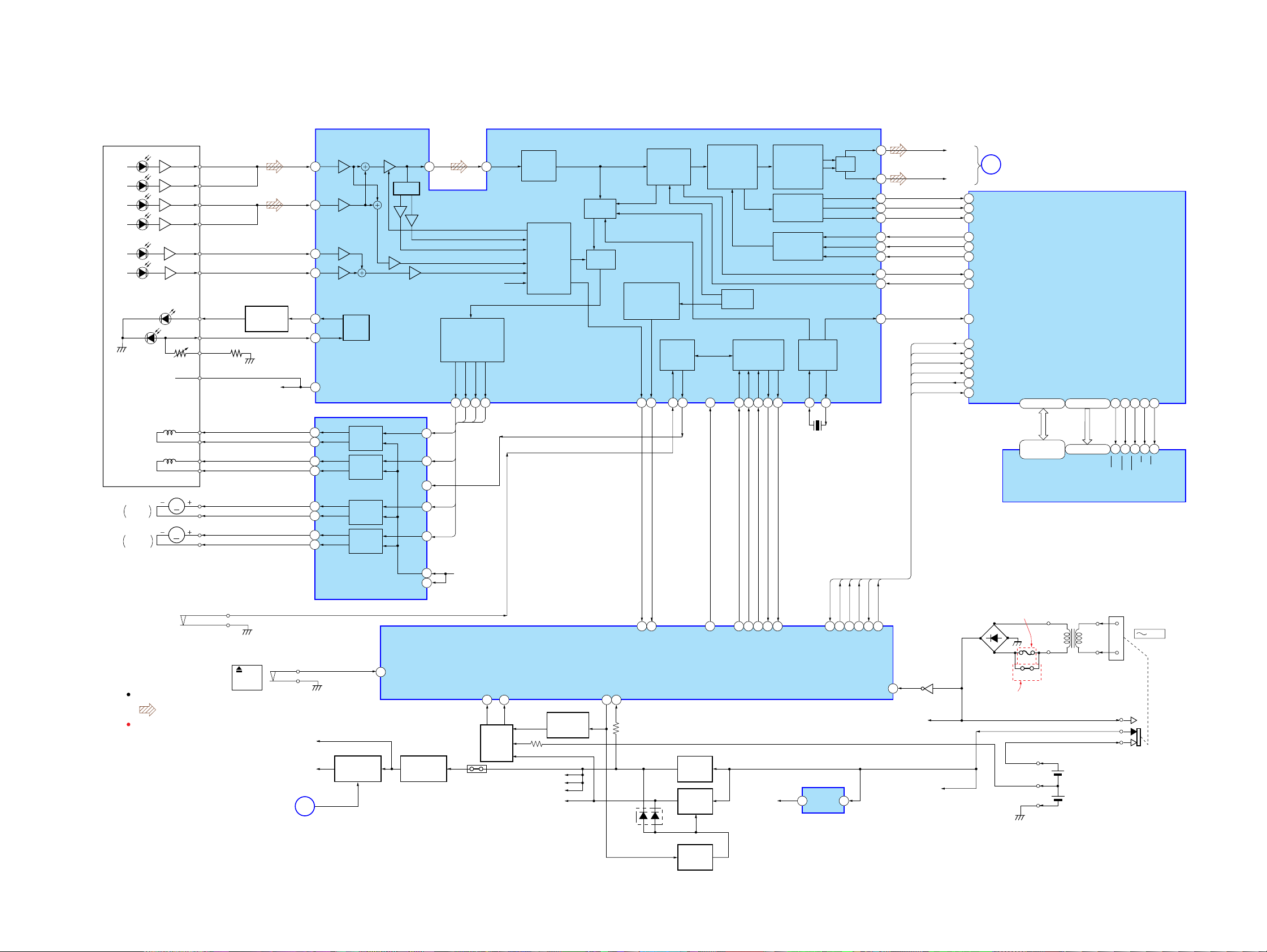
6-3. BLOCK DIAGRAM — CD SECTION —
A
C
B
D
E
F
LD
PD
VREF
OPTICAL PICK-UP
BLOCK
(KSS-213R)
TRACKING
COIL
FOCUS
COIL
M702
SLED
MOTOR
M701
SPINDLE
MOTOR
S701
(LIMIT)
M
M
Signal path
: CD
Abbreviation
CND : Canadian model
KR : Korean model
TW : Taiwan model
A
C
B
D
E
F
LD
PD
VR
VREF
T+
T–
F+
F–
SL+
SL–
SP+
SP–
CONTROLLER
S801
PUSH
OPEN/
CLOSE
LD POWER
Q701
VREF
COM. 3.3V
D.VDD (3.3V)
2
(Page 21)
FIN2
FIN1
7
TIN1
9
TIN2
10
LDD
80
LDS
79
VREF
11
T+
17
T–
18
F+
12
F–
11
SL+
26
SL–
27
SP+
2
SP–
1
SLED/SPINDLE
MOTOR DRIVER,
TRACKING/FOCUS
CD-CONT
APC
TRACKING
COIL
DRIVE
FOCUS
COIL
DRIVE
SLED
MOTOR
DRIVE
SPINDLE
MOTOR
DRIVE
COIL DRIVER
IC702
CD +3.3V
SWITCH
Q806,808
48
PH/BH
MUTE
CD DOOR
RF
TIN
20
FIN
10
SLIN
25
SPIN
VREF
23
OPIN
15
+3.3V
REG
Q957,D957
LCHO
RCHO
DATA
DATACK
LRSY
ASDFIN
ASDACK
ASLRCK
16MOUT
CE
CL
80CE70
CL(MP3)
CF2
RESB
INTB
79
49
INTB(MP3)
AC-CHK
42
45
59
58
57
56
55
52
50
RESB
44
AC-HI
CONT4
AUDIO+6V
REG
Q955,D953
POWER
SWITCH
Q952,953
INTERPOLATION
MUTE
&
ATTENUATION
DEEMPHASIS
PLL
VCEC
COMMAND
INTERFACE
RES
DICECL
DI(CD)
RES(CD)
CE(CD)
BATT COM
VDD
SLICE
LEVEL
CONTROL
A/D
CONVERTER,
SERVO
PROCESSOR
RF AMP,
SYSTEM SERVO PROCESSOR,
DIGITAL SIGNAL PROCESSOR
SYSTEM CONTROLLER
VH
59
CONTROLLER
Q807,D802
RADIO 6V
AUDIO 6V
P.VDD (6.2V)
VDD (SW)
IC701
IC801 (1/2)
POWER
CLV,CAV
CONTROL
SWITCH
93
P-CON58REG-CHK
D951
D/A
FDD
SPDO
21 22 23
FD
SP
ICP301
EFMIN
3
AGC
HFL
PH(RFENV)
FE
TE
VREF
SLDO
SL
VM
60
BATTERY
CHECK
Q804,805
48
CONVERTER
TDDTD
20
TD
FD
7
SL
SP
3
VREF
ERROR
CORRECTION
AUDIO CD
FRAME SYNC
DETECT,PROTECT
INSERT
EFM DECODER
GENERAL
PURPOSE
PORT
CONT1
FSEQ
DRF
67
31 72 25 66 63 61 62 49 48
72 77 74 76 75 50 7378
DRF(CD)
FSEQ(CD)
WRQ
65 64
CL(CD)
WRQ(CD)
3.3V
DIGITAL
FILTER
1-bit DAC
SERIAL
EXTERNAL
AUDIO IN
DO
DO(CD)
8FS
&
OUT
CLOCK
GENERATOR
XIN
16.93MHz
X701
+3.3V
IC803
REG
LPF
FSX/16MIN
XOUT
CMDIN
CMDOUT
69
68
CMDIN(MP3)
CMDOUT(MP3)
23
CMDOUT
CMDIN
CL
CE
INTB
RESB
Q803
U-COM
(VDD)
CD_IN_ L
CD_IN_R
1
7960
DATA IN
DATACK
80
1
LRSY
2
ADDATA
3
ADBCK
4
ADLRCK
5
CF2IN
CKOUT
9
CKIN
754
CMDOUT
73
74
CMDIN
75
CL
76
CE
INTB
77
78
RESB
CND,KR,TW MODEL
D901 – 904
RECT
(Page 21)
MDATA0
MDATA15
23-30,33-40 60-53,50
2-5,7-10,
35-38,40-43
DQ0-DQ15
F902
JW902
US MODEL
I
POWER
TRANSFORMER
4.5V
4.5V
MPS DECODER,
CD-ROM DECODER,
ANTI-SHOK
CONTROLLER
IC1001
MADRS0
I
MADRS8
18-21,24-28
A0-A8
SDRAM
IC1002
T901
DRY BATTERY
SIZE " D "
(IEC DESIGNATION R20)
6PCS,9V
OEB
CASLB
CASUB
RASB
41 44 43 45 42
16 30 31 29 15
OE
RAS
LCAS
UCAS
J901
AC IN
WEB
WE
POWER
SWITCH
Q951
2020
Page 21

6-4. BLOCK DIAGRAM — MAIN SECTION —
CD_IN_R
HRP301
RECORD/PLAYBACK
HEAD
L-CH
R-CH
HE301
ERASE HEAD
ANT1
FM
TELESCOPIC
ANTENNA
(Page 20)
3.3V
S301
(REC/PB)
REC
PB
RESET
2
AUDIO 6V
IC804
VDD (SW)
1
CD_IN_L
-1 -2
431
D324
CT3
TRACKING
RESET
D3
FERRITE-ROD
ANTENNA
CT3,L3
AM
98
REC-IN
FREQUENCY
COVERAGE
L3
AM
RADIO 6V
CT1,L1
FM
TRACKING
Q302
17
ISS1
L4
AM
RADIO 6V
22 4 6
2
RADIO 6V
Q303
AM
RF-IN
FM
RF-IN
L4
AM OSC
FM
RF-OUT
18
ISS2
EEPROM
PD
16
LP-IN
17
LP-OUT
18
AM
OSC
AM
MIX
D1 D2
EEPROM
-SDA
IC802
FM
MIX
FM
OSC
2124
R.RO
9
R.IN
8
R.LINE
14
4
24
5
6
T301
EEPROM
1112
65
11 12
FM OSC
L.RO
L.LINE
L.IN
REF
-SCL
AM IN
1920
RADIO 6V
FM IN
DET
REC
21 22 16
REC BIAS OSC
Q301
TU-CE
TU-CLK
TU-DATA
21 3 4
1 2 3 4
CEDICL
FM/AM FRONT END, IF AMP,
OSC-OUT
MIX-OUT
L2L1 CT1
FREQUENCY
COVERAGE
ALC 2
RADIO L
L.RAD
TU_IN_L
SYSTEM CONTROLLER
IC801 (2/2)
TU-COUNT
XT141XT2
42
DO
XOUT
T1
T1
AM IF
L2
FM
75kHz
FM MPX
IC1
RADIO 6V
RADIO 6V
XIN
X1
20 19
REC/PB
PRE AMP
IC301
R.RAD
TU_IN_R
39X138
NC
FM/AM PLL
IC2
CF4
CF2
L.LO
20
R-CH
18
17
15
TAPE
20
CD-ON
TAPE-ON
X2
FM/AM
OSC FREQ.
SHIFT SELECT
Q812,813
MO/ST10IF IN
13
14 17 13 18
LPF2/MO-ST
IF
BUFFER
IF-OUT
7
X801
5MHz
AM
IF-IN
FM
IF-IN
R.LO
LINE
TAPE
6
8
10
CD-CONT
IF CUT
AM
DET
FM
DET
10
RADIO 6V
SEL2
A2
B2
C2
2
(Page 20)
FM/AM SHIFT
35
7
BUFFER
QUAD
T2
3 2
BAND8ST-IND
ST-IND
LPF1/BAND
DET-OUT
AF
T2
FM IF
VOLUME/SOUND PROCESSOR
VIN2
LOGIC
SI
13SC14
9521 94
V-DATA
V-CLOCK
B-MUTE
5
16 15
IC303
TREBLE/
BASS
CONTROL
LED
DRIVER
Q810
D401
MP3
MPX-IN
MP3-LED
28
MPX
FM
VOUT2
IF CUT
MUTE
CFD-S20CP
POWER AMP
IC304
MUTE
Q124
91
49
A-MUTE
56
57
11 5
U-COM
(VDD)
LEVEL
DETECT
D323
TAPE PLAY
DETECT
TCPLAY
KEY5
KEY5
KEY4
KEY3
KEY2
KEY1
Q801
LCD-CLK33LCD-DATA32LCD-CS31LCD-C/D30LCD-RST
22 23 24 26 27
SCK
COM0-COM3
30-33
16
MEGA
BASS
CONTROLLER
Q122
D322
92
MEGA BASS
L-OUT
R-OUT
WAKE-UP
46
Q814,D804
12
11
KEY153KEY254KEY355KEY4
TU_IN_R
R-CH
VDD (SW)
RMC IN
29
SI
CS
C/D
RESET
S0-S27
34-41,43-55
1-8
LIQUID CRYSTAL
DISPLAY PANEL
ND401
KEY NETWORK
S401-406
S407-411
S412-417
S418-420
S425-431
LCD
DRIVER
IC401
VDD (SW)
Signal path
: FM
: AM
: TAPE PLAY
: TAPE REC
: CD
R-ch is omitted due to same as
L-ch.
45 1
AC-HI
D402
OPR/BATT
(TAPE PLAY)
M
M801
CAPSTAN/REEL
MOTOR
REMOTE
CONTROL
RECEIVER
IC402
D801
SP301
SPEAKER
(L-CH)
SP302
SPEAKER
(R-CH)
S802
3
J321
i
21 21
Page 22

CFD-S20CP
Ver 1.3
THIS NOTE IS COMMON FOR PRINTED WIRING
BOARDS AND SCHEMATIC DIAGRAMS.
(In addition to this, the necessary note is
printed in each block.)
Common Note on Schematic Diagrams:
• All capacitors are in µF unless otherwise noted. pF: µµF
50 WV or less are not indicated except for electrolytics
and tantalums.
• All resistors are in Ω and 1/
specified.
f
•
• C : panel designation.
Note:
The components identified by mark 0 or dotted
line with mark 0 are critical for safety.
Replace only with part
number specified.
• A : B+ Line.
• H : adjustment for repair.
•Total current is measured with no cassette installed.
•Power voltage is dc 9V and fed with regulated dc power
•Voltages are taken with a VOM (Input impedance 10 M Ω).
•Waveforms are taken with a oscilloscope.
• Circled numbers refer to waveforms.
• Signal path.
•Abbreviation
: internal component.
supply from battery terminal.
Voltage variations may be noted due to normal produc-
tion tolerances.
Voltage variations may be noted due to normal production tolerances.
F : FM
f : AM
E : PB
a : REC
J : CD
CND : Canadian model.
KR : Korean model.
TW : Taiwan model.
4
W or less unless otherwise
Note:
Les composants identifiés par
une marque 0 sont critiques
pour la sécurité.
Ne les remplacer que par une
piéce portant le numéro
spécifié.
6-5. PRINTED WIRING BOARD — CD SECTION — • Refer to page 19 for Circuit Boards Location.
9
2345678
1
A
B
C
D
E
Common Note on Printed Wiring Boards:
• X : parts extracted from the component side.
• Y : parts extracted from the conductor side.
f
•
• : Pattern from the side which enables seeing.
•Abbreviation
: internal component.
CND : Canadian model.
KR : Korean model.
TW : Taiwan model.
1-684-176-
F
G
H
11
(11)
2222
Page 23

CFD-S20CP
A
B
C
D
E
F
G
1
OPTICAL
PICK-UP
BLOCK
(KSS-213R)
2345678
R712
743
D701
FB707
FB706
FB705
FB702
R
M702
SLED
M
MOTOR
C731
C734
CNP702
(Page 27)
SPX
SLX
C720
FX
C718
C715
(TE)
TX
TP
C756
FY
SPY
SLY
C716
(FE)
TY
R740
TP
C719
C706
(VREF)
C701
C717
C721
R744
C704
C723
R707
R709
C711
C712
C740
TP
C714
C722
C729
C707
R759
TP(RF)
C713
C709
R710
R729
IC701
R730
R713
R708
R711
C732
Q701
C705
C710
R727
C746
FB701
X701
C733
C737
C708
R728
R765
C1014
R714
R726
C742
R715
R764
R763
R724
FB704
R761
R725
C744
C743
C762
R732
R1020
R1018
R1082
R762
(L-CH)
FB703
C767
TP
CNP701
C763
R733
R737
C766
C760
R734
C1011
R1017
R1019
TP
(R-CH)
C761
R735
R723
C764
C1012
R757
R745
C1068
R736
R1081
R755
R706
C1013
R1001
FB1001
C1074
C1010
C1037
R704
R1002
C1069
C1066
R1003
C1067
R702
C703
R1004
C1070
R1005
FB1002
IC702
C1030
C702
C1058
C1059
R1068
C1043
C747
C748
C753
R1075
R1074
C1042
D702
C1029
M701
SPINDLE
M
MOTOR
R758
R756
R703
C745
C750
R1079
R720
R721
R722
R1078
C1056
R705
R716
C752
R1077
R701
R719
C751
R1080
IC1001
R731
C1057
C1001
C1044
S701
C754
R717
C741
R1073
R753
R760
(LIMIT)
R718
R1076
C1004
C1031
9
• Semiconductor
Location
Ref. No. Location
D701 G-7
D702 F-7
IC701 D-3
IC702 B-7
IC1001 F-5
IC1002 H-6
Q701 B-3
H
IC1002
C1055
C1054
23 23
1-684-176-
11
(11)
Page 24

CFD-S20CP
6-6. SCHEMATIC DIAGRAM — CD SECTION — • Refer to page 22 for Common Note on Schematic Diagrams and page 38 for IC Block Diagrams.
S701
CNP701
R701
R702
R703
R704
R705
R706
R745
R755
R756
R757
R758
C703
C723
C707
C706
C702
C708
C710
R709 R710
C711
C712
C701
C715
C716
C718
C720
C705
C740
R727R728
R729R730
R708
R759R711
C714
C719
C717
Q701
R724
C709
C746
R707
C704
IC B/D
TP
C713
TP
TP
TP
C721
C744
726
R
764
R
C743
725
R
763
R
C756
C752
C753
C754
C751
C750
C745
C741
C742
IC701
R731
717
716
718
719
720
721
R
R
C722R740
722
R
R
R
R
R
FB704
X701
TP
66
C10
R1005
C1070
C1067
C1068
C1074
C1011
C760
C761
C762
C763
3
3
732
734
R
R
R73
R72
C767
C766
C764
R735
R736
R737
FB703
C737
R765
FB701
R713
C733
C732
C729
R715
R714
R762
R761
TP
R1001
C1069
R1002
R1003
R1004
FB1001
FB1002
C1010
R1017R1081
R1018
R1082
C1012
C1014
1080
R
R1019R1020
C1013
75
074
1076
R1
R10
R
R1078
79
077
1073
R1
R10
R
C1044
IC1001
C1037
R1068
C1043
C1056
C1001
C1057
C1058
C1059
C1004
C1042
D702
D701
C1031
C1030
C1029
M702
M701
•Voltage and waveforms are dc with respect to ground
under no-signal (detuned) conditions.
no mark : CD PLAY
R743
R712
R744
• Wavef orms (Mode: PLAY)
500mV/div 0.5µsec/div
1
0.85±0.2Vp-p
R760
R753
C748
C747
100mV/div 20µsec/div
2
IC B/D
IC702
100mV/div 20µsec/div
3
1.8V 1.8V
1V/div 0.05µsec/div
4
IC1002
3.2Vp-p
5
C1054
C1055
C731
C734
FB702
FB705
FB706
FB707
2V/div 50nsec/div
6Vp-p
6
(Page 28)
CNP702
2V/div 50nsec/div
5.2Vp-p
IC7014 (RF)
Approx. 100mVp-p
IC701qd (FE)
Approx. 100mVp-p
IC701qg (TE)
2424
16.93MHz
IC701rk (XOUT)
60nsec
IC701t; (FSX/16MIN (I))
60nsec
IC10017 (CKIN (I))
Page 25

6-7. PRINTED WIRING BOARD — TUNER SECTION — • Refer to page 19 for Circuit Boards Location and page 22 for Common Note on Printed Wiring Boards.
CFD-S20CP
Ver 1.3
A
B
C
D
E
F
G
1
(Page 27)
(Page 27)
234567891011 12 13 14
L3 AM FERRITE-ROD ANTENNA
US,CND MODEL
C32
KR,TW MODEL
R32
JC24
CT1
C13
IC1
C11
C80
C14
C15
C78
D1
C34
C35
L1
R2
C1
US,CND MODEL
C9
C7
C12
TP
FM
IN
C18
C4
JW12
T1
JW11
T2
JW13
D10
C8
R3
JC13
CF4
C10
R1
CF2
D11
CNP2
JW2
JC6
11
1-680-952- (11)
WHT
BLK
BLK
BLK
BLK
BLK
WHT
BLK
BLK
BLK
BLK
C26
C27
TP
(VT)
CNP1
JC1
R61
R60
R59
R58
C65
L21
JC33
R63
JC34
R10
JW3
C62
C63
R13
R65
R94
C60
C29
C61
C51
C66
C52
IC2
C68
X1
R56
C59
R53
JC2
R50
R52
C55
C57
R4
C53
C95
C37
R54
JC5
JW5
JW4
R51
C54
R91
JW6
JC4
JC11
C47
C39
JW7
R40
C41
CT3
C49
C42
L4
R11
C21
C43
JC3
JC12
R30
JW9
D3
C22
D2
C30
C56
R41
C33
L2
R31
C31
R24
C24
C23
C20
JW10
KR,TW MODEL
L11
JW8
R92
C77
ANT1
FM
TELESCOPIC
ANTENNA
• Semiconductor
Location
Ref. No. Location
D1 C-10
D2 D-8
D3 D-8
D10 B-12
D11 B-12
IC1 E-10
IC2 E-5
25 25
Page 26

CFD-S20CP
Ver 1.3
6-8. SCHEMATIC DIAGRAM — TUNER SECTION — • Refer to page 22 for Common Note on Schematic Diagrams and page 38 for IC Block Diagrams.
L3
D3
C34
CT3
R41 C49 C47R40
CT1
D1
C35 C33
L1
JC12 JC11
L11JC24
C41
C42
C43
R30R32 C80
C31
D2
L2
C30
R31
JC3
C39
C37
C24
L4
R11
C21 C22
R50
R91
C51 C52
X1
R52 R65
C53
R51
C59
R53
C54
R54
C95
C55
C65
R63
TP
C56
C57
IC B/D
R24
C13
C23
C20
IC2
IC B/D
JC13
C12
IC1
C7
C9
C61
C62
C63
R92
C66
C68
C60
R94
JC5
R4
R56
ANT1
TP
CNP2
C32 C4 C8
D11D10
C1
R2
R3
C10
•Voltage and waveforms are dc with respect to ground
under no-signal (detuned) conditions.
no mark : FM
(): AM
C11
C18
T2
C14 C15
C77 C78
JC4
JC33
JC2
JC34
C29
R10
R60R61 R59 R58
JC1
C27 C26
T1
CF4
JC6
R1
CF2
R13
L21
CNP1
(Page 28)
(Page 28)
• Wavef orm
0.5V/div 5µsec/div
1
1.5Vp-p
75kHz
IC2 w; (XOUT)
2626
Page 27

6-9. PRINTED WIRING BOARDS — MAIN SECTION — • Refer to page 19 for Circuit Boards Location and page 22 for Common Note on Printed Wiring Boards.
CFD-S20CP
Ver 1.3
A
B
C
D
E
F
G
H
1
(Page 25)
(Page 32)
S801
Z PUSH
OPEN/CLOSE
D804
C831
JC315
23456789101112
IC304
C128
C228
C126
L804
C229
Q224
R228
R248
C328
R819
R148
C139
C836
JW319
R332
C206
JC304
JC303
JC306
JC305
R882
R883
JW332
C838
C129
L803
R820
R130
C150
C239
R135
JW385
148
IC802
C837
C322
R149
C855
C146
C135
5
R821
R240
R125
C331
JW380
R890
R811
R814
R815
R816
C856
L801
R822
R244
Q124
R150
R133
R812
R806
R807
R808
R809
R810
R868
JW329
JW306
C132
R233
C133
R823
Q812
R144
C232
JW338
KR,TW
MODEL
JW386
JW327
C858
R825
R140
C235
JW321
JW339
X801
C820
C862
C130
R250
R249
C839
C804
R805
C859
IC804
JW318
R225
C246
R235
R879
C840
CN803
R804
C863
3
2
4
1
C233
R803
R826
JW317
JW353
R881
C841
JC317
C861
R824
JW352
C842
R802
JW326
R834
C230
C250
R335
R833
R334
C832
C843
C860
C821
Q813
C864
R844
JW316
JW366
C830
R877
R801
C822
JW379
JW384
C829
R851
IC801
R846
JW397
JW313
R960
C951
Q955
C952
R955
D953
R954
JW314
JW315
R325
C326
61
CN802
JW355
JW365
R813
R322
D322
JW387
C825
JW388
JW390
C827
C828
R876
JW359
JW393
R899
JW394
R875
R827
R873
C826
C803
JW360
R828
R874
R871
D805
R869
R872
R891
JW322
JW342
R326
C824
R837
D324
JW354
R841
R838
JW343
C953
R889
R836
R898
Q811
R897
JW363
JW344
JW324
JW310
R843
R842
R839
R870
JW362
R892
R896
JW312
Q802
JW305
R858
R857
R856
R855
R854
R852
R831
C846
C847
R840
JW311
R862
R861
R845
R860
R859
R853
R830
R895
JW341
JW340
C148
R893
JW348
JW395
C882
C849
JW349
Q953
C248
C848
JW309
JW325
JW328
R894
Q951
JW308
JW320
CNJ806
R952
R961
C881
R953
R962
JW391
R865
JW346
CNJ807
R956
R963
JW304
R957
R964
R951
JW369
JW368
JW367
JW357
JW356
JW307
JW333
JW350
Q952
JW358
D951
C801
R888
JW330
Q805
C131
R829
Q807
JC314
C231
D323
JW301
Q804
KH321
Q806
Q808
Q803
C325
KH301
R231
R131
C323
R959
C959
JW374
JW323
JW389
R850
Q801
D802
1-683-992-
JW303
JW302
JW392
R324
C880
JC311
R323
R887
C324
Q957
D801
ICP301
R958
R333
D957
C957
CNP801
C960
JW351
11
(11)
(Page 36)
(Page 23)
M
M801
CAPSTAN/
REEL
MOTOR
FB302
R132
S802
(TAPE PLAY)
R232
CNP322
J321
FB301
JW101
FB303
CNP323
1-683-999-
11
(11)
R886
JC310
R885
C823
C147
C327
CNJ804
Q810
D803
R884
C247
R847
R848
C852
R849
R864
R863
C222
JW361
JW373
JW371
JW372
JW382
R227
C225
C125
C122
C329
R880
JW375
C850
R127
C226
Q222
Q122
IC303
C321
C854
123
IC803
JW331
1
2
KH801
Q814
JW376
JW337
JW335
C834
C851
R128
JW396
R832
C857
JW334
R817
R818
R230
C106
US,
CND
MODEL
JW364
C853
C835
C833
R331
CNJ805
SP302
SP301
• Semiconductor
Location
Ref. No. Location
D322 D-6
D323 E-8
D324 C-6
D801 G-9
D802 H-9
D803 G-2
D804 G-2
D805 E-6
(D951) B-8
D953 B-6
D957 F-9
IC303 C-3
IC304 A-4
IC801 F-5
IC802 E-4
IC803 E-3
IC804 H-5
Q122 B-3
Q124 B-4
Q222 B-3
Q224 B-3
Q801 G-9
Q802 C-7
Q803 G-9
Q804 H-8
Q805 H-8
Q806 G-9
Q807 G-8
Q808 G-8
Q810 G-2
Q811 C-6
Q812 G-4
Q813 G-5
Q814 F-3
(Q951) B-7
Q952 B-8
Q953 B-7
Q955 B-5
Q957 E-9
( ) : CND, SP, KR model
I
(Page 34)
(Page 30)
27 27
Page 28

CFD-S20CP
Ver 1.3
6-10. SCHEMATIC DIAGRAM — MAIN SECTION (1/2) — • Refer to page 22 for Common Note on Schematic Diagrams and page 39 for IC Block Diagrams.
M801
S802
(Page 26)
(Page 26)
(Page 31)
R850
CNP801
CN802
CN803
C839
CNJ807
C880
C248
C148
C840
C843
C842
C841
C106 C206
C326
Q801
R889
JC304
JC306
IC803
C853
JC303
IC802
Q802
JC305
R812
R813
R814
R815
R816
IC B/D
R882
R804
R805
R883
Q811
L803
L804
R888
Q806
Q808
R865
C833
JC315
Q810
R827
CNJ806
CNJ804
KH801
CNJ805
(Page 24)
(Page 33)
S801
Q803
JC311
R884 R885
R886
R843
R842
R841
R840
R839
R836
R838
R837
C803
C823
D803
R862
R861
R845
R860
R859
R858
R857
R856
R855
R854
R853
R852
R849
C848
Q814(1/2)
JC310
D802
C849
R891
C850
C851
D804
C852
Q807
R894
R898
R899
R863
R864
D801
C824
C825
C826
C827
C828
C829
C830
R877
R876
R875
R822
R823
R874
C804
JC317
R851
R801
R802
R803
R806
R807
R808
R809
R810
R811
R881
R868
R817
R818
R890
C855C854
C856
R819
R820
R821
R873
R826
R872
R871
X801
IC801
R897
D805
R870
R828
C822
R869
R830
R831
Q804
R880
R879
R887
R829
C801
Q805
R896R895
C846
C847
R893
R892
R848
R846
R847
R844
C857
R832
C831
(Page 29)
• Waveform
1V/div 0.2µsec/div
1
IC801 ek (X2)
5MHz
C881
2.6Vp-p
C882
C862
Q812
C820
C858R825R824
C861C860
C821C859
Q813
C863
C864
R833
R834
IC804
L801
C832
C838
C837
C836
C835
C834
•Voltage and waveforms are dc with respect to ground
under no-signal (detuned) conditions.
no mark : FM
(): PB
<>: REC
[]: CD PLAY
2828
(Page 35)
Page 29

6-11. SCHEMATIC DIAGRAM — MAIN SECTION (2/2) — • Refer to page 22 for Common Note on Schematic Diagrams and page 39 for IC Block Diagrams.
C327
C147
C122
C222
C247
C328
C139
C239
C146
R135
C135
C246
R233R133
R235
C235
R334
R335
R332
R331
C329
IC B/D
IC303
C133
C233
C321
R127
C125
C225
R227
R150 C150
R125 R149
Q122
Q222
R225 R249
R250C250
R140
R148
R128
C126
C226
R228
R248
R240
Q124 Q224
C331
R230
C228
C229
C128
R130
C129
IC304
C322
C130
C131
C132
R144
C232
R244
C230
C231
R131
R231
KH301
CNP322
R232
R132
FB303
CNP323
FB302
FB301
CFD-S20CP
Ver 1.3
SP301
SP302
J321
(Page 28)
D324
R325
R326
C960
D322
R333
Q957
R322
C959
ICP301
D957
C957
R959
R958
Q955
R960
C953
C951
D953
R955 R954
C952
Q952
R951
R952
R953
Q953
R956
R957
JC314
D951
R961
R962
R963
R964
Q951
C323
C325
C324
R324
D323
R323
C324
R324
KH321
(Page 37)
29 29
•Voltage is dc with respect to ground under no-signal
(detuned) condition.
no mark : FM
(): PB
<>: REC
[]: CD PLAY
Page 30

CFD-S20CP
Ver 1.2
6-12. PRINTED WIRING BOARD — TC SECTION — • Refer to page 19 for Circuit Boards Location and page 22 for Common Note on Printed Wiring Boards.
A
B
C
D
E
S301
(REC/PB)
REC
PB
1
234567
• Semiconductor
Location
Ref. No. Location
IC301 C-4
Q301 B-3
Q302 B-5
Q303 B-5
R305
S301
C305
R308
C306
-1-2
T301
R314
R315
R210
R306
C102
C104
Q301
R202
C202
R110
C304
R203
C302
R102
C203
C204
R103
C207
C307
R204
C201
C107
C103
R307
R212
R104
C101
C308
C310
R206
C205
C105
R301
IC301
R201
R112
R106
R101
JC306
JC308
R111
C301
R205
R211
R310
JC302
JC303
R302
JC301
R303
R304
R105
R311
JC304
JC305
JC307
Q303
BLK
Q302
JC309
CN303
(Page 27)
R309
C303
F
G
YEL
RED
WHT
R-CH
L-CH
HRP301
RECORD/PLAYBACK
HEAD
1-681-594- (12)
12
BLK
(CHASSIS)
3030
Page 31

6-13. SCHEMATIC DIAGRAM — TC SECTION — • Refer to page 22 for Common Note on Schematic Diagrams and page 39 for IC Block Diagrams.
IC301
CFD-S20CP
Ver 1.2
R301
C102
C301
R110 R101
C104
C101
C107
C207
C201
C202
C204
R102
R103
C103
C203
R203R202
C302
R112
C105
C205R201R210
R104
R204
R212
R106
R206
R111
JC302
JC306
JC308
R211
R304
JC303
C303
R309
R105
R205
IC B/D
JC305
JC307
CN303
JC301
R303
R302
(Page 28)
• Wavef orms
0.1V/div 5µsec/div
1
19.5µsec
Q301 C (REC)
4Vp-p
C310 C308
10V/div 5µsec/div
2
19.5µsec
T301, HRP301 (YEL)
40Vp-p
R305
R314 R315
T301
C305
R308
Q303Q302
R311R310
C306
R306
C304
Q301
R307C307
JC304
JC309
•Voltage and waveforms are dc with respect to ground
under no-signal (detuned) conditions.
no mark : FM
(): PB
<>: REC
[]: CD PLAY
31 31
Page 32

CFD-S20CP
6-14. PRINTED WIRING BOARDS — CONTROL SECTION — • Refer to page 19 for Circuit Boards Location and page 22 for Common Note on Printed Wiring Boards.
A
B
C
D
S425
CD
1
R434
R433
R445
234567891011121314
S422
S427
TAPE
S426
RADIO BAND •
S421
MODE
AUTO PRESET
S428
S429
N X
R435
14
CNJ407
R444
R436
JC405
JC404
./
TUNE -
15
CNJ406
R437
S431
> /
TUNE +
R441
R440
14
CNJ408
S430
x
R438
R429
1-683-995-
DISPLAY •
ENT•
MEMORY
R430
S420
REPEAT
E
F
G
H
(Page 27)
S414
FOLDER +
D401
MP3
S415
FOLDER -
S418
CNJ405
R439
R426
R425
C414
R421
JW
403
R424
R423
POWER
R447
R443
I
R446
S419
SLEEP
S417
SOUND
CNJ404
R422
S413
VOL -
1-683-997-
J
1-683-996-
S416
MEGA
S412
VOL +
BASS
3232
Page 33

6-15. SCHEMATIC DIAGRAM — CONTROL SECTION — • Refer to page 22 for Common Note on Schematic Diagrams.
CFD-S20CP
S418
S419
(Page 28)
R443
R446
CNJ405
CNJ406
CNJ407
R444
JC405
S420
S425
S426
S427
S428
S429
CNJ408 CNJ404
R445
R433
R434
R435
JC404
R436
R447
R422
R423
R424
R425
R426
R439
R421
C414
S412
S413
S414
S415
S416
S417
D401
FA3864X
R429
R430
S421
S422
33 33
S430
S431
R437
R440
R438
R441
•Voltage is dc with respect to ground under no-signal
(detuned) condition.
no mark : FM
Page 34

CFD-S20CP
6-16. PRINTED WIRING BOARDS — DISPLAY SECTION — • Refer to page 19 for Circuit Boards Location and page 22 for Common Note on Printed Wiring Boards.
A
B
C
D
1
2345678910
• Semiconductor
Location
Ref. No. Location
D402
OPR/BATT
C403
R411
R412
C410
R413
IC401
R420
R442
1
5
10
15
20
R414
C408
C407
C406
C405
25
CNJ403
R428
81
30
R416
R417
R418
R419
JC402
32
R474
R473
C409
C413
R415
C415
JC407
JC406
C404
L401
D402 B-8
IC401 C-4
IC402 H-9
E
F
G
H
ND401 LIQUID CRYSTAL DISPLAY PANEL
R404
S404
4
R409
R471
R427
R470
S409
R403
R405
S403
3
R408
S408
JW401
R407
S402
2
R402
JW406
R448
R449
S401
JW408
1
R401
R406
JW404
S405
5
JW402
R410
S411
>10 0/10 9 8 7 6
R475
R469
S410
R472
1-683-993-
CNJ402
C402
IC402
123
S406S407
C401
JW405
CNJ401
1-683-994-
I
(Page 27)
3434
Page 35

6-17. SCHEMATIC DIAGRAM — DISPLAY SECTION — • Refer to page 22 for Common Note on Schematic Diagrams.
S406
R406
S405
R405
S411
CFD-S20CP
(Page 28)
CNJ401
R475
R469
IC402
C402
C401
R471
R470
R427
S404
S403
S402
S401
R404
R403
R402
R449
R401
S410
S409
S408
S407
R410
R409
R408
R407
R448
CNJ402
CNJ403
C415
R428
R472
R473
R474
JC406
L401
D402
JC407
C403
C404
C405
R415
JC402
C413
C406
C407
C408
C409
R411
R412
R413
R414
C410
R416
R417
R418
R419
ND401
R442R420
IC401
35 35
•Voltage is dc with respect to ground under no-signal
(detuned) condition.
no mark : FM
Page 36

CFD-S20CP
Ver 1.3
6-18. PRINTED WIRING BOARDS — POWER SUPPLY SECTION — • Refer to page 19 for Circuit Boards Location and page 22 for Common Note on Printed Wiring Boards.
A
B
C
D
1
J901
~ AC IN
2345678910 11 12
CNP904
RED
JW911
JW912
CNB901
DRY BATTERY
SIZE " D "
(IEC DESIGNATION R20)
6PCS, 9V
JW
JW
914
913
CND,KR,TW
MODEL
C902
D902
C904
F902
JW902
US MODEL
D901
C901
D904
C903
D903
JW904
JW905
C906
CNP902CNP901
(Page 27)
• Semiconductor
Location
Ref. No. Location
D901 B-3
D902 B-3
D903 C-4
D904 C-3
E
F
T901
POWER
TRANSFORMER
1-683-998-
RED
1-684-000-
1-684-001-
3636
Page 37

6-19. SCHEMATIC DIAGRAM — POWER SUPPLY SECTION — • Refer to page 22 for Common Note on Schematic Diagrams.
(Page 29)
CNP902
CFD-S20CP
Ver 1.3
J901
T901
F902
JW902
C904
D904
D903
C903
C902
D902
D901
C901
CNP904
C906
CNP901
CNB901
37 37
Page 38

CFD-S20CP
6-20. IC BLOCK DIAGRAMS
IC701 LC78646E-E (CD Board)
FIN1
FIN2
TIN1
TIN2
REFI
DEFECT
ADAVDD
ADAVSS
JITTC
SLCO
1
SLCO
SLCIST
EFMIN
RFVDD
RFVSS
VREF
RFMON
JITTC
ADAVDD
ADAVSS
FIN1
FIN2
TIN1
TIN2
REFI
TEC
TDO
SLCIST
2
EFMIN
3
RF
4
RF
5
6
FIN1
7
FIN2
8
TIN1
9
TIN2
10
VREF
11
REFI
12
FE
13
FE
TE
14
15
16
17
18
19
20
TEC
TE
RFMON
JITTC
ADAVDD
ADAVSS
TDO
PDO1
PDO2
FR
PCKIST
VVDD
VVSS
SBCK/FG
WRQ
CL
CE
DI
DO
CONT1-3
SBCK/CONT6
CONT4,5
LDS80LDD
79 78 77 76 75 74 73 72 71
LDS
LDD
+
–
+
–
+
–
+
–
LEVEL SET
A/D
SLICE LEVEL
CONTROL
PLL
VCEC
CLOCK
GENERATOR
COMMAND
INTERFACE
GENERAL PURPOSE
PORTS
8FS
DIGITAL FILTER
1BIT DAC
FDO
21 22 23 24 25 26 27 28 29 30 31 32 33 34 35 36 37 38
FR
VVDD
FR
VVDD
PCKIST
MIX
LPF
TBAL
TBAL
RAM
SERVO PROCESSOR
JITTER
DETECT
CLV,CAV
CONTROL
16MOUT
XVSS
XIN
XOUT
XVDD
SLDO
SPDO
CONT4
CONT5
GPDAC
FDO
SLDO
SPDO
CONT4
GPDAC
PCKIST
VVSS
PDO2
VVSS
PDO2
AGC
ERROR
CORRECTION
AUDIO CD
INTERPOLATION
ATTENUATION
DEEMPHASIS
SBCK/FG
SBCK/CONT6
CONT5
SBCK/FG
SBCK/CONT6
VSS
PDO1
CONT1
PDO1
CONT1
FE
MONITOR SIGNAL SELECTOR
MUTE
LPF
V/P
DEFECT
V/P
DEFECT
VDD5
CONT2
CONT3
69 68 67 66 65 64 63 62 61
70
CONT2
CONT3
TE
EQ
LPF
LPF
–
+
AUTO ADJUST
SW
DRF
RUPTURE DEFECT
FRAME SYNC
DETECT,PROTECT,INSERT,
EFM DECODE
SUBCODE DECODE CRC
FSEQ
MONI1
MONI2
MONI3
FSEQ
MONI1
MONI2
MONI3
DRF
RES
DRF
SW
+
–
TRACK JUMP
D/A
MONI4
MONI5
MONI4
MONI5
WRQDODICLCE
WRQDODICLCE
RF
TEC
PH
BH
S/H
RAM
EXTERNAL
AUDIO IN
SERIAL
OUT
AUDIO OUT
39 40
VSS
TEST
DOUT
VDD(3.3V)
MONI
CONT
APC
+
–
+
–
FDO
SPDO
SLDO
GPDAC
FSEQ
MONI1-5
V/P
RFMON
VREF
LDD
LDS
TDO
FSX/16MIN
ASDFIN
ASDACK
ASLRCK
DATACK
DRF
EFLG
DATA
LRSY
LVDD
LVSS
LCHO
RCHO
RVDD
RVSS
C2F
DATA
DATACK
LRSY
ASDFIN
ASDACK
ASLRCK
16MOUT
EFLG
C2F
XVSS
FSX/16MIN
XIN
XOUT
XVDD
RVDD
RCHO
RVSS
LVSS
LCHO
LVDD
60
59
58
57
56
55
54
53
52
51
50
49
48
47
46
45
44
43
42
41
DATA
DATACK
LRSY
ASDFIN
ASDACK
ASLRCK
16MOUT
EFLG
C2F
XVSS
FSX/16MIN
XIN
XOUT
XVDD
RVDD
RCHO
RVSS
LVSS
LCHO
LVDD
IC702 BA5826FP-E2 (CD Board) IC1 TA2149BN (TUNER Board)
GND1
1
SP–
SP+
SPIN
RST
REG–B
REGO
MUTE
GND
(TIN)
GND
OPOUT
TIN
28
1
D.BUFF
2
D.BUFF
3
4
THERMAL
SHUT-DOWN
MONITOR
5
6
7
8
9
10
D.BUFF
T–
11
D.BUFF
T+
12
13
14
DRIVER
MUTE
LEVEL
SHIFT
REGULATOR
LEVEL
SHIFT
LEVEL
SHIFT
LEVEL
SHIFT
D.BUFF
D.BUFF
VCC
VCC
D.BUFF
D.BUFF
GND
27
SL–
SL+
26
25
SLIN
24
(SLIN)
23
VREF
VCC
22
VCC
21
20
(FIN)
FIN
19
F–
18
F+
17
NC
16
OPIN
15
FM RF-IN
AM LOW CUT
MIX OUT
VCC2
AF IF-IN
FM IF-IN
GND2
AGC
QUAD
R-OUT
L-OUT
FM RF
2
3
4
5
6
7
8
9
10
11
MUTE
12
AM IF
FM IF
AGC
FM
MIX
AM
MIX
IC2 LC72137M-TLM (TUNER Board)
CE
1
DI
2
CCB
3
4
5
6
7
8
9
10
UNIVERSAL
COUNTER
I/F
PROGRAMMABLE
LATCH
DATA SHIFT REGISTER
12BITS
DIVIDER
UNLOCK
DETECTOR
SWALLOW
COUNTER
1/16,1/17
4BITS
REFERENCE
DIVIDER
PHASE
DETECTOR
CHARGE
PUMP
POWER ON
RESET
1/2
20
XOUT
XIN
19
18
LP-OUT
17
LP-IN
PD
16
VSS
15
14
VDD
MO/ST
13
FM IN
12
AM IN
11
CL
DO
MUTE
FM/AM
BAND
ST-IND
BAND
IF IN
LEVEL
DET
AM
DET
FM
DET
ST/MO
FM/AM
24
FM RF-OUT
23
VCC1
AM RF-IN
22
FM
OSC
AM
OSC
BUFF
BUFF
IF BUFF
1/8
AF BUFF
VCO
DIVIDE
DECODE
ST
SW
IF REQ
1/1 OR
1/16
AF
16
15
21
20
19
18
17
14
13
FM OSC
ST-IND
AM OSC
OSC-OUT
IF-OUT
DET-OUT
MPX- IN
LPF2/MO-ST
LPF1/BAND
3838
Page 39

IC802 CAT24WC02JI-1.8-TE13 (MAIN Board)
CFD-S20CP
1K BIT EEPROM ARRAY
7BIT
START STOP
VOLTAGE DETECTION
GND
1
A0
7BIT
ADDRESS
A1
2
A2
3
4
DECODER
CONTROL CIRCUIT
HIGH VOLTAGE
OCCURENCE CIRCUIT
IC303 BD3870FS-E2 (MAIN Board)
CAP
24
SURROUND
TNF1
23
TREBLE1
0
=8kHz
f
TREBLE2
0
=8kHz
f
SLAVE • WORD
ADDRESS
REGISTER
POWER SUPPLY
TNF2
22
8
VCC/2
7
6
5
VCC
WP
SCL
SDA
OUT1
OUT2
VCC
SI
LOGIC
8BIT
DATA
REGISTER
ACK
BNF2
BOUT2
21 20 19 18 17 16 15 14 13
BASS2
f0=80Hz
BNF1
BASS1
0
=80Hz
f
BOUT1
SC
VCC/2
VCC/2 VCC/2
1 2 3 4
VIN1
IC301 TA2068N (TC Board)
1
AGC
2
L.PO
L.NF
L.RO
L.IN
REF
GND
R.IN
R.RO
R.NF
R.PO
MIC.NF
3
4
5
6
REF
AMP
7
8
9
10
11
12
REC
AMP1
2.1
NAB
AMP2
26dB
REC
AMP2
26dB
MIC
AMP1
DET
NAB
AMP1
ALC2 ALC1
ON
VIN2
BUF AMP
MUTE
BUF AMP
A1
SEL2
A2
5 6 7 8 9 10 11 12
SEL1
TAPE
BUF AMP
BUF AMP
TAPE
A1
TAPE
B1
B2
TAPE
LINE
RADIO
MUTE
ON
ON
MUTE
RADIO
LINE
A2
MONITOR
AMP
7dB
7dB
MONITOR
AMP
B1
LOGIC
24
23
22
21
20
19
18
17
16
15
14
13
B2
L.RAD
MIC I/EX
L.LINE
REC
L.LO
VCC
R.LO
LINE
R.LINE
TAPE
R.RAD
MIC
C1
C2
VCC/2
FILTER
GND
39
Page 40

CFD-S20CP
Ver 1.3
NOTE:
• The mechanical parts with no reference
number in the exploded views are not supplied.
• Items marked “*” are not stocked since
they are seldom required for routine service.
Some delay should be anticipated
when ordering these items.
•Abbreviation
CND : Canadian model
KR : Korean model
TW : Taiwan model
7-1. MAIN SECTION
SECTION 7
EXPLODED VIEWS
• Color Indication of Appearance Parts
Example :
KNOB, BALANCE (WHITE) ... (RED)
R
Parts Color Cabinet’s Color
• Accessories are given in the last of this parts list.
R
The components identified by
mark 0 or dotted line with mark
0 are critical for safety.
Replace only with part number
specified.
Les composants identifiés par une
marque 0 sont critiques pour
la sécurité.
Ne les remplacer que par une piéce
portant le numéro spécifié.
3
3
3
4
2
#1
3
5
3
3
1
Ref. No. Part No. Description Remark
1 3-237-699-41 LID, BATTERY (US,CND)
1 3-237-699-51 LID, BATTERY (KR,TW)
2 3-237-726-11 PLATE (L) (KR,TW)
2 3-237-726-31 PLATE (L) (US,CND)
3 4-951-620-81 SCREW (2.6)
40
Ref. No. Part No. Description Remark
4 3-237-700-11 HANDLE (KR,TW)
4 3-237-700-31 HANDLE (US,CND)
5 3-237-727-11 PLATE (R) (KR,TW)
5 3-237-727-31 PLATE (R) (US,CND)
#1 7-685-533-19 SCREW +BTP 2.6X6 TYPE2 N-S
Page 41

7-2. CABINET FRONT SECTION
SP301
#2
69
68
67
CFD-S20CP
Ver 1.3
66
65
ND401
62
63
55
72
54
56
57
70
59
58
61
53
#2
71
59
MD block
59
60
64
59
#2
#2
SP302
51
52
Ref. No. Part No. Description Remark Ref. No. Part No. Description Remark
51 X-3382-002-1 DOOR SUB ASSY, CASSETTE (US,CND)
51 X-3382-175-1 DOOR SUB ASSY, CASSETTE (KR,TW)
52 3-237-694-31 HOLDER, CASSETTE (KR,TW)
52 3-237-694-51 HOLDER, CASSETTE (US,CND)
53 3-040-916-01 FOOT (FRONT), RUBBER
54 X-3382-003-1 FRONT SUB ASSY, CABINET (US)
54 X-3382-176-1 FRONT SUB ASSY, CABINET (TW)
54 X-3382-178-1 FRONT SUB ASSY, CABINET (CND)
54 X-3382-302-1 FRONT SUB ASSY, CABINET (KR)
55 3-242-758-01 HOLDER (LCD)
* 56 1-683-993-11 LCD BOARD
57 1-824-342-11 CABLE, FLEXIBLE FLAT 8P (CNJ403)
58 3-237-725-01 SPRING, CASSETTE
59 4-951-620-11 SCREW (2.6X10), +BVTP
60 3-047-468-11 DAMPER (US,CND)
61 4-951-620-31 SCREW (2.6), +BVTP
62 3-237-709-41 WINDOW, LCD (KR,TW)
62 3-237-709-61 WINDOW, LCD (US,CND)
* 63 1-683-994-11 CONTROL (4) BOARD
64 3-237-707-31 BUTTON, REC
65 3-237-706-31 BUTTON, PLAY
66 3-237-704-31 BUTTON, REW
67 3-237-705-31 BUTTON, FF
68 3-237-703-31 BUTTON, S/E
69 3-237-702-31 BUTTON, PAUSE
70 3-831-441-11 CUSHION (B)
71 3-243-185-11 CUSHION
72 1-824-344-11 CABLE, FLEXIBLE FLAT (13 CORE)
ND401 1-804-712-11 DISPLAY PANEL, LIQUID CRYSTAL
SP301 1-825-031-11 SPEAKER (10cm) (L-CH)
SP302 1-825-031-11 SPEAKER (10cm) (R-CH)
#2 7-685-647-79 SCREW +BVTP 3X10 TYPE2 N-S
41
Page 42

CFD-S20CP
Ver 1.3
7-3. CABINET TOP SECTION
109
108
106
110
111
#1
123
105
121
122
107
107
107
104
101
103
102
121
116
114
115
118
117
#3
115
KSM-213RDP
117
116
119
113
112
S801
124
125
122
120
107
Ref. No. Part No. Description Remark Ref. No. Part No. Description Remark
* 101 1-683-995-11 CONTROL (1) BOARD
102 1-824-340-11 CABLE, FLEXIBLE FLAT 4P (CNJ408)
103 1-824-341-11 CABLE, FLEXIBLE FLAT 5P (CNJ406)
104 1-824-339-11 CABLE, FLEXIBLE FLAT 4P (CNJ407)
* 105 1-683-996-11 CONTROL (2) BOARD
106 3-922-112-41 DAMPER
107 4-951-620-01 SCREW (2.6X8), +BVTP
108 3-019-395-01 PLATE, CHUCKING
109 1-452-899-11 MAGNET
110 3-240-598-21 LID, CD (US,CND)
110 3-240-598-31 LID, CD (KR,TW)
111 3-245-184-01 SPRING, CD
112 X-3382-004-1 TOP SUB ASSY, CABINET (US)
112 X-3382-179-1 TOP SUB ASSY, CABINET (CND)
112 X-3382-303-1 TOP SUB ASSY, CABINET (KR,TW)
* 113 A-3323-787-A CD BOARD, COMPLETE
114 3-923-736-01 COVER, CD
115 3-931-379-21 RUBBER, VIBRATION PROOF
116 3-921-725-11 SCREW (2.6X10), +PWH
117 3-931-379-31 RUBBER, VIBRATION PROOF
118 1-757-689-11 CABLE, FLEXIBLE FLAT (16 CORE)
119 1-824-345-11 CABLE, FLEXIBLE FLAT 20P
* 120 1-683-997-11 CONTROL (3) BOARD
121 3-220-756-01 CUSHION (BUTTON)
122 3-831-441-11 CUSHION (B)
123 3-040-315-01 COVER (AC OUT)
124 3-244-257-01 ILLUMINATOR
125 3-240-288-01 TUBE, DIFFUSION
S801 1-692-960-11 SWITCH, PUSH (1 KEY)
(Z PUSH OPEN/CLOSE)
#1 7-685-533-19 SCREW +BTP 2.6X6 TYPE2 N-S
#3 7-685-853-04 SCREW +BVTT 2X6 (S)
42
Page 43

7-4. CABINET REAR SECTION
159
157
160
164
157
#4
CFD-S20CP
Ver 1.3
ANT1
161
#4
#5
165
162
T901
167
157
158
166
152
153
157
163
154
157
156
155
166
Ref. No. Part No. Description Remark Ref. No. Part No. Description Remark
* 151 1-684-000-11 BATTERY (1) BOARD
152 4-960-167-01 SCREW (3X8) (DIA.10), +WH
153 3-240-561-01 TERMINAL (–), BATTERY
154 3-237-724-01 TERMINAL, ANTENNA (CNP2)
* 155 A-3323-778-A TUNER BOARD, COMPLETE (US,CND)
153
165
152
The components identified by
mark 0 or dotted line with mark
0 are critical for safety.
Replace only with part number
specified.
* 162 1-684-001-11 BATTERY (2) BOARD
163 3-240-597-51 REAR, CABINET (US)
163 3-240-597-61 REAR, CABINET (CND)
163 3-240-597-71 REAR, CABINET (KR,TW)
164 1-824-343-11 CABLE, FLEXIBLE FLAT 13P
151
Les composants identifiés par une
marque 0 sont critiques pour
la sécurité.
Ne les remplacer que par une piéce
portant le numéro spécifié.
* 155 A-3323-815-A TUNER BOARD, COMPLETE (KR,TW)
156 3-249-551-01 HOLDER (PWB TU)
157 4-951-620-11 SCREW (2.6X10), +BVTP
* 158 1-683-998-11 POWER BOARD
159 3-921-725-11 SCREW (2.6X10), +PWH
* 160 1-683-999-11 HEADPHONE BOARD
* 161 A-3178-741-A MAIN BOARD, COMPLETE (KR,TW)
* 161 A-3323-783-A MAIN BOARD, COMPLETE (US)
* 161 A-3323-961-A MAIN BOARD, COMPLETE (CND)
165 3-018-963-01 CUSHION (BATTERY CASE LID)
166 3-846-312-01 SPACER
* 167 3-703-044-26 LABEL, CAUTION (CND)
ANT1 1-754-241-11 ANTENNA, TELESCOPIC (FM)
0 T901 1-435-918-21 TRANSFORMER, POWER (KR)
0 T901 1-437-351-21 TRANSFORMER, POWER (CND,TW)
0 T901 1-437-540-11 TRANSFORMER, POWER (US)
#4 7-685-645-79 SCREW +BVTP 3X6 TYPE2 N-S
#5 7-682-548-04 SCREW +B 3X8
43
Page 44

CFD-S20CP
d
Ver 1.2
7-5. TAPE MECHANISM SECTION
201
210
202
HRP301
204
not supplied
203
M801
204
205
206
209
#6
not supplie
207
208
#6
Ref. No. Part No. Description Remark Ref. No. Part No. Description Remark
201 3-244-086-01 ARM ASSY, PINCH ROLLER
202 3-244-079-01 BELT (B), SUB
203 3-244-080-01 BELT (B), MAIN
204 3-244-083-01 SCREW BIND DT M2X6
205 3-244-084-01 SCREW PAN M2.6X4.5
206 3-237-718-01 LEVER, REC
* 207 A-3323-806-A TC BOARD, COMPLETE
208 3-237-719-01 CHASSIS, TC
209 3-030-741-01 SCREW (M2X2)
210 A-3013-956-A MF-S200
HRP301 3-244-085-01 HEAD, R/P (REC/PB)
M801 3-244-082-01 MOTOR ASSY (CAPSTAN/REEL)
#6 7-685-851-04 SCREW +BVTT 2X4 (S)
44
Page 45

7-6. CD MECHANISM SECTION
(KSM-213RDP)
CFD-S20CP
Ver 1.1
253
254
251
255 255
257
M701
M702
The components identified by
mark 0 or dotted line with mark
0 are critical for safety.
Replace only with part number
specified.
252
256
Les composants identifiés par une
marque 0 sont critiques pour
la sécurité.
Ne les remplacer que par une piéce
portant le numéro spécifié.
Ref. No. Part No. Description Remark
251 2-626-908-01 SHAFT, SLED
* 252 2-647-408-02 GEAR (B)
0 253 8-820-161-02 PICK-UP, OPTICAL KSS-213R/C2RP
* 254 2-169-065-01 GEAR (A)
255 2-169-388-01 TAPPING (M2), +PWB
Ref. No. Part No. Description Remark
256 X-2162-707-1 CHASSIS ASSY (RDP) (RP), MOTOR (SPINDLE)
(including M701)
257 3-713-786-51 SCREW (M2X3)
M702 X-2162-712-1 GEAR ASSY (R) (RP), MOTOR (SLED)
45
Page 46

CFD-S20CP
Ver 1.3
BA TTERY (1)
SECTION 8
ELECTRICAL PARTS LIST
BA TTERY (2)
NOTE:
• Due to standardization, replacements in
the parts list may be different from the
parts specified in the diagrams or the
components used on the set.
• -XX and -X mean standardized parts, so
they may have some difference from the
original one.
• RESISTORS
All resistors are in ohms.
METAL:Metal-film resistor.
METAL OXIDE: Metal oxide-film resistor.
F:nonflammable
• Items marked “*” are not stocked since
they are seldom required for routine service.
Some delay should be anticipated
when ordering these items.
Ref. No. Part No. Description Remark Ref. No. Part No. Description Remark
* 1-684-000-11 BATTERY (1) BOARD
3-240-561-01 TERMINAL (–), BATTERY
*************************************************************
* 1-684-001-11 BATTERY (2) BOARD
3-240-561-01 TERMINAL (–), BATTERY
* CNP904 1-815-550-11 PIN, CONNECTOR (PWB) 2P
*************************************************************
* A-3323-787-A CD BOARD, COMPLETE
C701 1-164-156-11 CERAMIC CHIP 0.1uF 25V
C702 1-104-665-11 ELECT 100uF 20% 10V
C703 1-164-156-11 CERAMIC CHIP 0.1uF 25V
C704 1-126-947-11 ELECT 47uF 20% 10V
C705 1-162-964-11 CERAMIC CHIP 0.001uF 10% 50V
C706 1-164-156-11 CERAMIC CHIP 0.1uF 25V
C707 1-104-665-11 ELECT 100uF 20% 10V
C708 1-107-826-11 CERAMIC CHIP 0.1uF 10% 16V
C709 1-104-665-11 ELECT 100uF 20% 10V
C710 1-165-176-11 CERAMIC CHIP 0.047uF 10% 16V
C711 1-107-826-11 CERAMIC CHIP 0.1uF 10% 16V
C712 1-162-923-11 CERAMIC CHIP 47PF 5% 50V
C713 1-162-968-11 CERAMIC CHIP 0.0047uF 10% 50V
C714 1-164-156-11 CERAMIC CHIP 0.1uF 25V
C715 1-126-960-11 ELECT 1uF 20% 50V
C716 1-162-964-11 CERAMIC CHIP 0.001uF 10% 50V
C717 1-162-968-11 CERAMIC CHIP 0.0047uF 10% 50V
C718 1-115-156-11 CERAMIC CHIP 1uF 10V
C719 1-162-968-11 CERAMIC CHIP 0.0047uF 10% 50V
C720 1-162-927-11 CERAMIC CHIP 100PF 5% 50V
C721 1-164-156-11 CERAMIC CHIP 0.1uF 25V
C722 1-164-156-11 CERAMIC CHIP 0.1uF 25V
C723 1-104-665-11 ELECT 100uF 20% 10V
C729 1-126-927-11 ELECT 2200uF 20% 10V
C731 1-162-968-11 CERAMIC CHIP 0.0047uF 10% 50V
C732 1-162-970-11 CERAMIC CHIP 0.01uF 10% 25V
C733 1-162-970-11 CERAMIC CHIP 0.01uF 10% 25V
CD
*****************
*****************
< CONNECTOR >
*******************
< CAPACITOR >
• SEMICONDUCTORS
In each case, u : µ, for example:
uA.. : µA.. uPA.. : µPA..
uPB.. : µPB.. uPC.. : µPC.. uPD.. : µPD..
• CAPACITORS
uF : µF
• COILS
uH : µH
•Abbreviation
CND : Canadian model
KR : Korean model
TW : Taiwan model
C734 1-162-968-11 CERAMIC CHIP 0.0047uF 10% 50V
C737 1-162-970-11 CERAMIC CHIP 0.01uF 10% 25V
C740 1-164-156-11 CERAMIC CHIP 0.1uF 25V
C741 1-115-156-11 CERAMIC CHIP 1uF 10V
C742 1-164-156-11 CERAMIC CHIP 0.1uF 25V
C743 1-165-176-11 CERAMIC CHIP 0.047uF 10% 16V
C744 1-115-156-11 CERAMIC CHIP 1uF 10V
C745 1-162-923-11 CERAMIC CHIP 47PF 5% 50V
C746 1-164-156-11 CERAMIC CHIP 0.1uF 25V
C747 1-164-156-11 CERAMIC CHIP 0.1uF 25V
C748 1-126-935-11 ELECT 470uF 20% 10V
C750 1-162-919-11 CERAMIC CHIP 22PF 5% 50V
C751 1-162-923-11 CERAMIC CHIP 47PF 5% 50V
C752 1-162-923-11 CERAMIC CHIP 47PF 5% 50V
C753 1-162-923-11 CERAMIC CHIP 47PF 5% 50V
C754 1-162-923-11 CERAMIC CHIP 47PF 5% 50V
C756 1-162-923-11 CERAMIC CHIP 47PF 5% 50V
C760 1-162-923-11 CERAMIC CHIP 47PF 5% 50V
C761 1-162-923-11 CERAMIC CHIP 47PF 5% 50V
C762 1-162-923-11 CERAMIC CHIP 47PF 5% 50V
C763 1-162-923-11 CERAMIC CHIP 47PF 5% 50V
C764 1-162-923-11 CERAMIC CHIP 47PF 5% 50V
C766 1-162-923-11 CERAMIC CHIP 47PF 5% 50V
C767 1-162-919-11 CERAMIC CHIP 22PF 5% 50V
C1001 1-162-923-11 CERAMIC CHIP 47PF 5% 50V
C1004 1-162-923-11 CERAMIC CHIP 47PF 5% 50V
C1010 1-164-156-11 CERAMIC CHIP 0.1uF 25V
C1011 1-164-156-11 CERAMIC CHIP 0.1uF 25V
C1012 1-115-156-11 CERAMIC CHIP 1uF 10V
C1013 1-164-156-11 CERAMIC CHIP 0.1uF 25V
C1014 1-104-665-11 ELECT 100uF 20% 10V
C1029 1-126-916-11 ELECT 1000uF 20% 6.3V
C1030 1-164-156-11 CERAMIC CHIP 0.1uF 25V
C1031 1-164-156-11 CERAMIC CHIP 0.1uF 25V
C1037 1-164-156-11 CERAMIC CHIP 0.1uF 25V
C1042 1-104-665-11 ELECT 100uF 20% 10V
C1043 1-164-156-11 CERAMIC CHIP 0.1uF 25V
C1044 1-164-156-11 CERAMIC CHIP 0.1uF 25V
C1054 1-126-935-11 ELECT 470uF 20% 10V
C1055 1-164-156-11 CERAMIC CHIP 0.1uF 25V
C1056 1-115-156-11 CERAMIC CHIP 1uF 10V
C1057 1-162-923-11 CERAMIC CHIP 47PF 5% 50V
C1058 1-162-923-11 CERAMIC CHIP 47PF 5% 50V
C1059 1-162-923-11 CERAMIC CHIP 47PF 5% 50V
C1066 1-162-923-11 CERAMIC CHIP 47PF 5% 50V
The components identified by
mark 0 or dotted line with mark
0 are critical for safety.
Replace only with part number
specified.
Les composants identifiés par une
marque 0 sont critiques pour
la sécurité.
Ne les remplacer que par une piéce
portant le numéro spécifié.
When indicating parts by reference
number, please include the board.
46
Page 47

CFD-S20CP
Ver 1.2
CD
Ref. No. Part No. Description Remark Ref. No. Part No. Description Remark
C1067 1-162-923-11 CERAMIC CHIP 47PF 5% 50V
C1068 1-162-923-11 CERAMIC CHIP 47PF 5% 50V
C1069 1-162-923-11 CERAMIC CHIP 47PF 5% 50V
C1070 1-162-923-11 CERAMIC CHIP 47PF 5% 50V
C1074 1-162-919-11 CERAMIC CHIP 22PF 5% 50V
R721 1-216-809-11 METAL CHIP 100 5% 1/10W
R722 1-216-809-11 METAL CHIP 100 5% 1/10W
R723 1-216-809-11 METAL CHIP 100 5% 1/10W
R724 1-216-841-11 METAL CHIP 47K 5% 1/10W
R725 1-216-817-11 METAL CHIP 470 5% 1/10W
< CONNECTOR >
CNP701 1-779-553-21 CONNECTOR, FFC (LIF(NON-ZIF)) 16P
CNP702 1-784-742-11 CONNECTOR, FFC 20P
< DIODE >
D701 8-719-988-61 DIODE 1SS355TE-17
D702 8-719-988-61 DIODE 1SS355TE-17
< FERRITE BEAD >
FB701 1-469-701-21 FERRITE, EMI (SMD)
FB702 1-469-701-21 FERRITE, EMI (SMD)
FB703 1-469-701-21 FERRITE, EMI (SMD)
FB704 1-469-701-21 FERRITE, EMI (SMD)
FB705 1-469-701-21 FERRITE, EMI (SMD)
FB706 1-469-701-21 FERRITE, EMI (SMD)
FB707 1-469-701-21 FERRITE, EMI (SMD)
FB1001 1-469-701-21 FERRITE, EMI (SMD)
FB1002 1-469-701-21 FERRITE, EMI (SMD)
< IC >
IC701 6-701-796-01 IC LC78646E-E
IC702 6-701-787-11 IC BA5826FP-E2
IC1001 6-701-791-01 IC LC78683E-US-E
IC1002 8-759-597-78 IC MSM54V16258BSL-40TSK
R726 1-216-817-11 METAL CHIP 470 5% 1/10W
R727 1-216-825-11 METAL CHIP 2.2K 5% 1/10W
R728 1-216-833-11 METAL CHIP 10K 5% 1/10W
R729 1-216-813-11 METAL CHIP 220 5% 1/10W
R730 1-216-821-11 METAL CHIP 1K 5% 1/10W
R731 1-216-825-11 METAL CHIP 2.2K 5% 1/10W
R732 1-216-809-11 METAL CHIP 100 5% 1/10W
R733 1-216-809-11 METAL CHIP 100 5% 1/10W
R734 1-216-809-11 METAL CHIP 100 5% 1/10W
R735 1-216-809-11 METAL CHIP 100 5% 1/10W
R736 1-216-809-11 METAL CHIP 100 5% 1/10W
R737 1-216-809-11 METAL CHIP 100 5% 1/10W
R740 1-216-809-11 METAL CHIP 100 5% 1/10W
R743 1-216-829-11 METAL CHIP 4.7K 5% 1/10W
R744 1-216-845-11 METAL CHIP 100K 5% 1/10W
R745 1-216-809-11 METAL CHIP 100 5% 1/10W
R753 1-216-829-11 METAL CHIP 4.7K 5% 1/10W
R755 1-216-829-11 METAL CHIP 4.7K 5% 1/10W
R756 1-216-829-11 METAL CHIP 4.7K 5% 1/10W
R757 1-216-829-11 METAL CHIP 4.7K 5% 1/10W
R758 1-216-829-11 METAL CHIP 4.7K 5% 1/10W
R759 1-216-809-11 METAL CHIP 100 5% 1/10W
R760 1-216-825-11 METAL CHIP 2.2K 5% 1/10W
R761 1-216-805-11 METAL CHIP 47 5% 1/10W
R762 1-216-805-11 METAL CHIP 47 5% 1/10W
< TRANSISTOR >
Q701 8-729-054-57 TRANSISTOR KTN2907AS-RTK
< RESISTOR >
R701 1-216-841-11 METAL CHIP 47K 5% 1/10W
R702 1-216-833-11 METAL CHIP 10K 5% 1/10W
R703 1-216-833-11 METAL CHIP 10K 5% 1/10W
R704 1-216-833-11 METAL CHIP 10K 5% 1/10W
R705 1-216-833-11 METAL CHIP 10K 5% 1/10W
R706 1-216-841-11 METAL CHIP 47K 5% 1/10W
R707 1-216-797-11 METAL CHIP 10 5% 1/10W
R708 1-216-833-11 METAL CHIP 10K 5% 1/10W
R709 1-216-837-11 METAL CHIP 22K 5% 1/10W
R710 1-216-829-11 METAL CHIP 4.7K 5% 1/10W
R711 1-216-813-11 METAL CHIP 220 5% 1/10W
R712 1-216-825-11 METAL CHIP 2.2K 5% 1/10W
R713 1-216-821-11 METAL CHIP 1K 5% 1/10W
R714 1-216-809-11 METAL CHIP 100 5% 1/10W
R715 1-216-809-11 METAL CHIP 100 5% 1/10W
R716 1-216-809-11 METAL CHIP 100 5% 1/10W
R717 1-216-809-11 METAL CHIP 100 5% 1/10W
R718 1-216-809-11 METAL CHIP 100 5% 1/10W
R719 1-216-809-11 METAL CHIP 100 5% 1/10W
R720 1-216-809-11 METAL CHIP 100 5% 1/10W
R763 1-216-813-11 METAL CHIP 220 5% 1/10W
R764 1-216-813-11 METAL CHIP 220 5% 1/10W
R765 1-216-841-11 METAL CHIP 47K 5% 1/10W
R1001 1-216-809-11 METAL CHIP 100 5% 1/10W
R1002 1-216-809-11 METAL CHIP 100 5% 1/10W
R1003 1-216-809-11 METAL CHIP 100 5% 1/10W
R1004 1-216-809-11 METAL CHIP 100 5% 1/10W
R1005 1-216-809-11 METAL CHIP 100 5% 1/10W
R1017 1-216-825-11 METAL CHIP 2.2K 5% 1/10W
R1018 1-216-809-11 METAL CHIP 100 5% 1/10W
R1019 1-216-821-11 METAL CHIP 1K 5% 1/10W
R1020 1-216-821-11 METAL CHIP 1K 5% 1/10W
R1068 1-216-825-11 METAL CHIP 2.2K 5% 1/10W
R1073 1-216-809-11 METAL CHIP 100 5% 1/10W
R1074 1-216-809-11 METAL CHIP 100 5% 1/10W
R1075 1-216-809-11 METAL CHIP 100 5% 1/10W
R1076 1-216-809-11 METAL CHIP 100 5% 1/10W
R1077 1-216-809-11 METAL CHIP 100 5% 1/10W
R1078 1-216-809-11 METAL CHIP 100 5% 1/10W
R1079 1-216-809-11 METAL CHIP 100 5% 1/10W
R1080 1-216-809-11 METAL CHIP 100 5% 1/10W
R1081 1-216-821-11 METAL CHIP 1K 5% 1/10W
R1082 1-216-805-11 METAL CHIP 47 5% 1/10W
47
Page 48

CFD-S20CP
CONTROL (4)CD CONTROL (1) CONTROL (2) CONTROL (3)
Ref. No. Part No. Description Remark Ref. No. Part No. Description Remark
< SWITCH >
R446 1-216-817-11 METAL CHIP 470 5% 1/10W
S701 1-571-936-11 SWITCH, LEAF (LIMIT)
< VIBRATOR >
X701 1-795-563-21 VIBRATOR, CERAMIC (16.9MHz)
*************************************************************
* 1-683-995-11 CONTROL (1) BOARD
******************
1-824-339-11 CABLE, FLEXIBLE FLAT 4P (CNJ407)
1-824-340-11 CABLE, FLEXIBLE FLAT 4P (CNJ408)
1-824-341-11 CABLE, FLEXIBLE FLAT 5P (CNJ406)
< JUMPER RESISTOR >
JC404 1-216-864-11 METAL CHIP 0 5% 1/10W
JC405 1-216-864-11 METAL CHIP 0 5% 1/10W
< RESISTOR >
R429 1-216-821-11 METAL CHIP 1K 5% 1/10W
R430 1-216-825-11 METAL CHIP 2.2K 5% 1/10W
R433 1-216-813-11 METAL CHIP 220 5% 1/10W
R434 1-216-821-11 METAL CHIP 1K 5% 1/10W
R435 1-216-821-11 METAL CHIP 1K 5% 1/10W
R436 1-216-825-11 METAL CHIP 2.2K 5% 1/10W
R437 1-216-821-11 METAL CHIP 1K 5% 1/10W
R438 1-216-825-11 METAL CHIP 2.2K 5% 1/10W
R440 1-216-825-11 METAL CHIP 2.2K 5% 1/10W
R441 1-216-829-11 METAL CHIP 4.7K 5% 1/10W
< SWITCH >
S418 1-786-050-21 SWITCH, KEYBOARD (POWER)
S419 1-786-050-21 SWITCH, KEYBOARD (SLEEP)
*************************************************************
* 1-683-997-11 CONTROL (3) BOARD
******************
3-240-288-01 TUBE, DIFFUSION
3-244-257-01 ILLUMINATOR
3-831-441-11 CUSHION (B)
< CAPACITOR >
C414 1-162-970-11 CERAMIC CHIP 0.01uF 10% 25V
< CONNECTOR >
CNJ404 1-784-726-11 CONNECTOR, FFC 4P
< DIODE >
D401 6-500-306-01 LED FA3864X (MP3)
< RESISTOR >
R421 1-216-809-11 METAL CHIP 100 5% 1/10W
R422 1-216-813-11 METAL CHIP 220 5% 1/10W
R423 1-216-821-11 METAL CHIP 1K 5% 1/10W
R424 1-216-821-11 METAL CHIP 1K 5% 1/10W
R425 1-216-825-11 METAL CHIP 2.2K 5% 1/10W
R444 1-216-821-11 METAL CHIP 1K 5% 1/10W
R445 1-216-817-11 METAL CHIP 470 5% 1/10W
< SWITCH >
S420 1-786-050-21 SWITCH, KEYBOARD (REPEAT)
S421 1-786-050-21 SWITCH, KEYBOARD (MODE)
S422 1-786-050-21 SWITCH, KEYBOARD (DISPLAY•ENT•MEMORY)
S425 1-786-050-21 SWITCH, KEYBOARD (CD)
S426 1-786-050-21 SWITCH, KEYBOARD (RADIO BAND•
AUTO PRESET)
S427 1-786-050-21 SWITCH, KEYBOARD (TAPE)
S428 1-786-050-21 SWITCH, KEYBOARD (./TUNE –)
S429 1-786-050-21 SWITCH, KEYBOARD (N X)
S430 1-786-050-21 SWITCH, KEYBOARD (x)
S431 1-786-050-21 SWITCH, KEYBOARD (>/TUNE +)
*************************************************************
* 1-683-996-11 CONTROL (2) BOARD
******************
3-831-441-11 CUSHION (B)
< CONNECTOR >
CNJ405 1-784-726-11 CONNECTOR, FFC 4P
< RESISTOR >
R426 1-216-821-11 METAL CHIP 1K 5% 1/10W
R439 1-216-825-11 METAL CHIP 2.2K 5% 1/10W
R447 1-216-817-11 METAL CHIP 470 5% 1/10W
< SWITCH >
S412 1-786-050-21 SWITCH, KEYBOARD (VOL +)
S413 1-786-050-21 SWITCH, KEYBOARD (VOL –)
S414 1-786-050-21 SWITCH, KEYBOARD (FOLDER +)
S415 1-786-050-21 SWITCH, KEYBOARD (FOLDER –)
S416 1-786-050-21 SWITCH, KEYBOARD (MEGA BASS)
S417 1-786-050-21 SWITCH, KEYBOARD (SOUND)
*************************************************************
* 1-683-994-11 CONTROL (4) BOARD
******************
< CAPACITOR >
C401 1-164-156-11 CERAMIC CHIP 0.1uF 25V
C402 1-126-785-11 ELECT 47uF 20% 10V
< CONNECTOR >
CNJ401 1-784-735-11 CONNECTOR, FFC 13P
CNJ402 1-770-516-31 CONNECTOR, FFC 8P
< IC >
R443 1-216-813-11 METAL CHIP 220 5% 1/10W
48
IC402 6-600-070-01 IC PIC-37041TE2
Page 49

CFD-S20CP
LCDHEADPHONECONTROL (4)
Ref. No. Part No. Description Remark Ref. No. Part No. Description Remark
< RESISTOR >
R401 1-216-817-11 METAL CHIP 470 5% 1/10W
R402 1-216-821-11 METAL CHIP 1K 5% 1/10W
R403 1-216-821-11 METAL CHIP 1K 5% 1/10W
R404 1-216-825-11 METAL CHIP 2.2K 5% 1/10W
R405 1-216-821-11 METAL CHIP 1K 5% 1/10W
* 1-683-993-11 LCD BOARD
**********
1-824-342-11 CABLE, FLEXIBLE FLAT 8P (CNJ403)
3-242-758-01 HOLDER (LCD)
< CAPACITOR >
R406 1-216-825-11 METAL CHIP 2.2K 5% 1/10W
R407 1-216-817-11 METAL CHIP 470 5% 1/10W
R408 1-216-821-11 METAL CHIP 1K 5% 1/10W
R409 1-216-821-11 METAL CHIP 1K 5% 1/10W
R410 1-216-825-11 METAL CHIP 2.2K 5% 1/10W
R427 1-216-821-11 METAL CHIP 1K 5% 1/10W
R448 1-216-813-11 METAL CHIP 220 5% 1/10W
R449 1-216-813-11 METAL CHIP 220 5% 1/10W
R469 1-216-845-11 METAL CHIP 100K 5% 1/10W
R470 1-216-821-11 METAL CHIP 1K 5% 1/10W
R471 1-216-821-11 METAL CHIP 1K 5% 1/10W
R475 1-216-849-11 METAL CHIP 220K 5% 1/10W
< SWITCH >
S401 1-786-050-21 SWITCH, KEYBOARD (1)
S402 1-786-050-21 SWITCH, KEYBOARD (2)
S403 1-786-050-21 SWITCH, KEYBOARD (3)
S404 1-786-050-21 SWITCH, KEYBOARD (4)
S405 1-786-050-21 SWITCH, KEYBOARD (5)
S406 1-786-050-21 SWITCH, KEYBOARD (6)
S407 1-786-050-21 SWITCH, KEYBOARD (7)
S408 1-786-050-21 SWITCH, KEYBOARD (8)
S409 1-786-050-21 SWITCH, KEYBOARD (9)
S410 1-786-050-21 SWITCH, KEYBOARD (0/10)
S411 1-786-050-21 SWITCH, KEYBOARD (>10)
*************************************************************
C403 1-162-974-11 CERAMIC CHIP 0.01uF 50V
C404 1-126-964-11 ELECT 10uF 20% 50V
C405 1-162-974-11 CERAMIC CHIP 0.01uF 50V
C406 1-107-826-11 CERAMIC CHIP 0.1uF 10% 16V
C407 1-107-826-11 CERAMIC CHIP 0.1uF 10% 16V
C408 1-107-826-11 CERAMIC CHIP 0.1uF 10% 16V
C409 1-162-962-11 CERAMIC CHIP 470PF 10% 50V
C410 1-162-962-11 CERAMIC CHIP 470PF 10% 50V
C413 1-164-227-11 CERAMIC CHIP 0.022uF 10% 25V
C415 1-162-970-11 CERAMIC CHIP 0.01uF 10% 25V
< DIODE >
D402 6-500-198-01 LED BT-233D-31 (OPR/BATT)
< IC >
IC401 8-759-153-90 IC uPD7225GB-3B7
< JUMPER RESISTOR >
JC402 1-216-864-11 METAL CHIP 0 5% 1/10W
JC406 1-216-864-11 METAL CHIP 0 5% 1/10W
JC407 1-216-864-11 METAL CHIP 0 5% 1/10W
< COIL >
L401 1-410-509-11 INDUCTOR 10uH
< LIQUID CRYSTAL DISPLAY >
* 1-683-999-11 HEADPHONE BOARD
*****************
< CONNECTOR >
* CNP322 1-815-444-11 PIN, CONNECTOR (PWB) 3P
CNP323 1-815-445-11 PIN, CONNECTOR (PWB) 4P
< FERRITE BEAD >
FB301 1-469-701-21 FERRITE, EMI (SMD)
FB302 1-469-701-21 FERRITE, EMI (SMD)
FB303 1-469-701-21 FERRITE, EMI (SMD)
< JACK >
J321 1-815-325-11 JACK (i)
< RESISTOR >
R132 1-216-809-11 METAL CHIP 100 5% 1/10W
R232 1-216-809-11 METAL CHIP 100 5% 1/10W
*************************************************************
ND401 1-804-712-11 DISPLAY PANEL, LIQUID CRYSTAL
< RESISTOR >
R411 1-216-833-11 METAL CHIP 10K 5% 1/10W
R412 1-216-833-11 METAL CHIP 10K 5% 1/10W
R413 1-216-833-11 METAL CHIP 10K 5% 1/10W
R414 1-216-833-11 METAL CHIP 10K 5% 1/10W
R415 1-216-837-11 METAL CHIP 22K 5% 1/10W
R416 1-216-864-11 METAL CHIP 0 5% 1/10W
R417 1-216-864-11 METAL CHIP 0 5% 1/10W
R418 1-216-833-11 METAL CHIP 10K 5% 1/10W
R419 1-216-833-11 METAL CHIP 10K 5% 1/10W
R420 1-216-845-11 METAL CHIP 100K 5% 1/10W
R428 1-216-813-11 METAL CHIP 220 5% 1/10W
R442 1-216-841-11 METAL CHIP 47K 5% 1/10W
R472 1-216-821-11 METAL CHIP 1K 5% 1/10W
R473 1-216-821-11 METAL CHIP 1K 5% 1/10W
R474 1-216-821-11 METAL CHIP 1K 5% 1/10W
*************************************************************
49
Page 50

CFD-S20CP
Ver 1.3
MAIN
Ref. No. Part No. Description Remark Ref. No. Part No. Description Remark
* A-3178-741-A MAIN BOARD, COMPLETE (KR,TW)
* A-3323-783-A MAIN BOARD, COMPLETE (US)
* A-3323-961-A MAIN BOARD, COMPLETE (CND)
*********************
7-685-645-79 SCREW +BVTP 3X6 TYPE2 N-S
< CAPACITOR >
C106 1-126-960-11 ELECT 1uF 20% 50V
C122 1-162-964-11 CERAMIC CHIP 0.001uF 10% 50V
C125 1-162-966-11 CERAMIC CHIP 0.0022uF 10% 50V
C126 1-126-960-11 ELECT 1uF 20% 50V
C128 1-162-964-11 CERAMIC CHIP 0.001uF 10% 50V
C129 1-126-947-11 ELECT 47uF 20% 10V
C130 1-104-665-11 ELECT 100uF 20% 10V
C131 1-126-926-11 ELECT 1000uF 20% 10V
C132 1-107-826-11 CERAMIC CHIP 0.1uF 10% 16V
C133 1-126-963-11 ELECT 4.7uF 20% 50V
C135 1-107-826-11 CERAMIC CHIP 0.1uF 10% 16V
C139 1-162-966-11 CERAMIC CHIP 0.0022uF 10% 50V
C146 1-164-156-11 CERAMIC CHIP 0.1uF 25V
C147 1-126-963-11 ELECT 4.7uF 20% 50V
C148 1-115-156-11 CERAMIC CHIP 1uF 10V
C150 1-162-970-11 CERAMIC CHIP 0.01uF 10% 25V
C206 1-126-960-11 ELECT 1uF 20% 50V
C222 1-162-964-11 CERAMIC CHIP 0.001uF 10% 50V
C225 1-162-966-11 CERAMIC CHIP 0.0022uF 10% 50V
C226 1-126-960-11 ELECT 1uF 20% 50V
C228 1-162-964-11 CERAMIC CHIP 0.001uF 10% 50V
C229 1-126-947-11 ELECT 47uF 20% 10V
C230 1-104-665-11 ELECT 100uF 20% 10V
C231 1-126-926-11 ELECT 1000uF 20% 10V
C232 1-107-826-11 CERAMIC CHIP 0.1uF 10% 16V
C233 1-126-963-11 ELECT 4.7uF 20% 50V
C235 1-164-156-11 CERAMIC CHIP 0.1uF 25V
C239 1-162-966-11 CERAMIC CHIP 0.0022uF 10% 50V
C246 1-164-156-11 CERAMIC CHIP 0.1uF 25V
C247 1-126-963-11 ELECT 4.7uF 20% 50V
C248 1-115-156-11 CERAMIC CHIP 1uF 10V
C250 1-162-970-11 CERAMIC CHIP 0.01uF 10% 25V
C321 1-104-665-11 ELECT 100uF 20% 10V
C322 1-126-947-11 ELECT 47uF 20% 10V
C323 1-126-964-11 ELECT 10uF 20% 50V
C324 1-162-974-11 CERAMIC CHIP 0.01uF 50V
(US,CND)
C324 1-164-245-11 CERAMIC CHIP 0.015uF 10% 25V
(KR,TW)
C325 1-126-937-11 ELECT 4700uF 20% 16V
C326 1-126-934-11 ELECT 220uF 20% 16V
C327 1-126-947-11 ELECT 47uF 20% 10V
C328 1-126-959-11 ELECT 0.47uF 20% 50V
C329 1-162-974-11 CERAMIC CHIP 0.01uF 50V
C331 1-126-934-11 ELECT 220uF 20% 10V
C801 1-126-947-11 ELECT 47uF 20% 10V
C803 1-162-964-11 CERAMIC CHIP 0.001uF 10% 50V
C804 1-162-964-11 CERAMIC CHIP 0.001uF 10% 50V
C820 1-162-908-11 CERAMIC CHIP 3PF 0.25PF 50V
C821 1-162-908-11 CERAMIC CHIP 3PF 0.25PF 50V
C822 1-162-962-11 CERAMIC CHIP 470PF 10% 50V
C823 1-104-665-11 ELECT 100uF 20% 10V
C824 1-162-927-11 CERAMIC CHIP 100PF 5% 50V
C825 1-162-927-11 CERAMIC CHIP 100PF 5% 50V
C826 1-162-927-11 CERAMIC CHIP 100PF 5% 50V
C827 1-162-927-11 CERAMIC CHIP 100PF 5% 50V
C828 1-162-927-11 CERAMIC CHIP 100PF 5% 50V
C829 1-162-927-11 CERAMIC CHIP 100PF 5% 50V
C830 1-162-927-11 CERAMIC CHIP 100PF 5% 50V
C831 1-162-927-11 CERAMIC CHIP 100PF 5% 50V
C832 1-162-927-11 CERAMIC CHIP 100PF 5% 50V
C833 1-162-927-11 CERAMIC CHIP 100PF 5% 50V
C834 1-162-974-11 CERAMIC CHIP 0.01uF 50V
C835 1-162-974-11 CERAMIC CHIP 0.01uF 50V
C836 1-162-974-11 CERAMIC CHIP 0.01uF 50V
C837 1-162-927-11 CERAMIC CHIP 100PF 5% 50V
C838 1-162-927-11 CERAMIC CHIP 100PF 5% 50V
C839 1-162-964-11 CERAMIC CHIP 0.001uF 10% 50V
C840 1-162-927-11 CERAMIC CHIP 100PF 5% 50V
C841 1-162-964-11 CERAMIC CHIP 0.001uF 10% 50V
C842 1-162-964-11 CERAMIC CHIP 0.001uF 10% 50V
C843 1-162-970-11 CERAMIC CHIP 0.01uF 10% 25V
C846 1-162-927-11 CERAMIC CHIP 100PF 5% 50V
C847 1-162-927-11 CERAMIC CHIP 100PF 5% 50V
C848 1-162-927-11 CERAMIC CHIP 100PF 5% 50V
C849 1-162-927-11 CERAMIC CHIP 100PF 5% 50V
C850 1-162-927-11 CERAMIC CHIP 100PF 5% 50V
C851 1-162-927-11 CERAMIC CHIP 100PF 5% 50V
C852 1-162-927-11 CERAMIC CHIP 100PF 5% 50V
C853 1-162-970-11 CERAMIC CHIP 0.01uF 10% 25V
C854 1-104-665-11 ELECT 100uF 20% 10V
C855 1-126-964-11 ELECT 10uF 20% 50V
C856 1-107-826-11 CERAMIC CHIP 0.1uF 10% 16V
C857 1-162-927-11 CERAMIC CHIP 100PF 5% 50V
C858 1-162-921-11 CERAMIC CHIP 33PF 5% 50V
C859 1-162-921-11 CERAMIC CHIP 33PF 5% 50V
C860 1-162-921-11 CERAMIC CHIP 33PF 5% 50V
C861 1-162-921-11 CERAMIC CHIP 33PF 5% 50V
C862 1-162-970-11 CERAMIC CHIP 0.01uF 10% 25V
C863 1-162-970-11 CERAMIC CHIP 0.01uF 10% 25V
C864 1-162-970-11 CERAMIC CHIP 0.01uF 10% 25V
C880 1-164-156-11 CERAMIC CHIP 0.1uF 25V
C881 1-126-963-11 ELECT 4.7uF 20% 50V
C882 1-126-963-11 ELECT 4.7uF 20% 50V
C951 1-162-974-11 CERAMIC CHIP 0.01uF 50V
C952 1-162-974-11 CERAMIC CHIP 0.01uF 50V
C953 1-126-935-11 ELECT 470uF 20% 10V
C957 1-162-974-11 CERAMIC CHIP 0.01uF 50V
C959 1-104-665-11 ELECT 100uF 20% 10V
C960 1-164-156-11 CERAMIC CHIP 0.1uF 25V
< CONNECTOR >
CNJ804 1-784-766-11 CONNECTOR, FFC 5P
CNJ805 1-784-774-11 CONNECTOR, FFC 13P
CNJ806 1-784-781-11 CONNECTOR, FFC 20P
CNJ807 1-784-774-11 CONNECTOR, FFC 13P
50
Page 51

CFD-S20CP
Ver 1.3
MAIN
Ref. No. Part No. Description Remark Ref. No. Part No. Description Remark
CNP801 1-815-445-11 PIN, CONNECTOR (PWB) 4P
< TRANSISTOR >
< DIODE >
D322 8-719-988-61 DIODE 1SS355TE-17
D323 8-719-988-61 DIODE 1SS355TE-17
D324 8-719-988-61 DIODE 1SS355TE-17
D801 8-719-082-07 DIODE KDS121-RTK
D802 8-719-082-07 DIODE KDS121-RTK
D803 8-719-069-54 DIODE UDZS-TE-17-5.1B
D804 8-719-083-93 DIODE KDS120-RTK
D805 8-719-988-61 DIODE 1SS355TE-17
D951 8-719-083-93 DIODE KDS120-RTK
D953 8-719-978-33 DIODE DTZ-TT11-6.8B
D957 8-719-083-58 DIODE UDZS-TE-17-3.9B
< IC >
IC303 6-701-824-11 IC BD3870FS-E2
IC304 8-759-426-51 IC BA5417
IC801 6-801-938-01 IC uPD784216AGF-527-3BA
IC802 6-700-336-01 IC CAT24WC02JI-1.8-TE13
IC803 8-759-658-46 IC S-81233SGY-Z
IC804 8-759-544-01 IC S-80828ANNP-EDR-T2
< IC LINK >
0 ICP301 1-533-674-11 LINK, CHIP IC (0.5A)
< JUMPER RESISTOR >
JC303 1-216-864-11 METAL CHIP 0 5% 1/10W
JC304 1-216-864-11 METAL CHIP 0 5% 1/10W
JC305 1-216-864-11 METAL CHIP 0 5% 1/10W
JC306 1-216-864-11 METAL CHIP 0 5% 1/10W
JC310 1-216-864-11 METAL CHIP 0 5% 1/10W
JC311 1-216-864-11 METAL CHIP 0 5% 1/10W
JC314 1-216-864-11 METAL CHIP 0 5% 1/10W
JC315 1-216-864-11 METAL CHIP 0 5% 1/10W
JC317 1-216-864-11 METAL CHIP 0 5% 1/10W
(KR,TW)
(US,CND)
(KR,TW)
(US,CND)
Q122 8-729-905-34 TRANSISTOR 2SC4081-Q
Q124 8-729-029-10 TRANSISTOR DTC143TUA-T106
Q222 8-729-905-34 TRANSISTOR 2SC4081-Q
Q224 8-729-029-10 TRANSISTOR DTC143TUA-T106
Q801 8-729-028-99 TRANSISTOR DTC114YUA-T106
Q802 8-729-028-76 TRANSISTOR DTA114YUA-T106
Q803 8-729-028-99 TRANSISTOR DTC114YUA-T106
Q804 8-729-028-76 TRANSISTOR DTA114YUA-T106
Q805 8-729-028-76 TRANSISTOR DTA114YUA-T106
Q806 8-729-922-10 TRANSISTOR 2SA1577-QR
Q807 8-729-028-99 TRANSISTOR DTC114YUA-T106
Q808 8-729-028-99 TRANSISTOR DTC114YUA-T106
Q810 8-729-028-76 TRANSISTOR DTA114YUA-T106
Q811 8-729-028-99 TRANSISTOR DTC114YUA-T106
Q812 8-729-905-34 TRANSISTOR 2SC4081-Q
Q813 8-729-905-34 TRANSISTOR 2SC4081-Q
Q814 8-729-028-92 TRANSISTOR DTA144TUA-T106
Q951 8-729-029-13 TRANSISTOR DTC143ZUA-T106
Q952 8-729-040-76 TRANSISTOR KTA1273-Y-AT
Q953 8-729-029-09 TRANSISTOR DTC143EUA-T106
Q955 8-729-021-82 TRANSISTOR 2SD2396K
Q957 8-729-028-54 TRANSISTOR KTC3205-AT
< RESISTOR >
R125 1-216-825-11 METAL CHIP 2.2K 5% 1/10W
R127 1-216-833-11 METAL CHIP 10K 5% 1/10W
R128 1-216-817-11 METAL CHIP 470 5% 1/10W
R130 1-216-813-11 METAL CHIP 220 5% 1/10W
R131 1-216-829-11 METAL CHIP 4.7K 5% 1/10W
R133 1-216-829-11 METAL CHIP 4.7K 5% 1/10W
R135 1-216-853-11 METAL CHIP 470K 5% 1/10W
R140 1-216-825-11 METAL CHIP 2.2K 5% 1/10W
R144 1-216-789-11 METAL CHIP 2.2 5% 1/10W
R148 1-216-813-11 METAL CHIP 220 5% 1/10W
R149 1-216-821-11 METAL CHIP 1K 5% 1/10W
R150 1-216-825-11 METAL CHIP 2.2K 5% 1/10W
R225 1-216-825-11 METAL CHIP 2.2K 5% 1/10W
R227 1-216-833-11 METAL CHIP 10K 5% 1/10W
R228 1-216-817-11 METAL CHIP 470 5% 1/10W
< CABLE HOLDER >
KH301 1-824-027-11 HOLDER, CABLE 3P
KH321 1-824-029-11 HOLDER, CABLE 4P
KH801 1-824-028-11 HOLDER, CABLE 2P
< COIL >
L801 1-414-142-61 INDUCTOR 1uH
L803 1-410-509-11 INDUCTOR 10uH
L804 1-414-142-61 INDUCTOR 1uH
R230 1-216-813-11 METAL CHIP 220 5% 1/10W
R231 1-216-829-11 METAL CHIP 4.7K 5% 1/10W
R233 1-216-829-11 METAL CHIP 4.7K 5% 1/10W
R235 1-216-853-11 METAL CHIP 470K 5% 1/10W
R240 1-216-825-11 METAL CHIP 2.2K 5% 1/10W
R244 1-216-789-11 METAL CHIP 2.2 5% 1/10W
R248 1-216-813-11 METAL CHIP 220 5% 1/10W
R249 1-216-821-11 METAL CHIP 1K 5% 1/10W
R250 1-216-825-11 METAL CHIP 2.2K 5% 1/10W
R322 1-216-833-11 METAL CHIP 10K 5% 1/10W
The components identified by
mark 0 or dotted line with mark
0 are critical for safety.
Replace only with part number
specified.
Les composants identifiés par une
marque 0 sont critiques pour
la sécurité.
Ne les remplacer que par une piéce
portant le numéro spécifié.
51
Page 52

CFD-S20CP
Ver 1.3
MAIN
Ref. No. Part No. Description Remark Ref. No. Part No. Description Remark
R323 1-216-857-11 METAL CHIP 1M 5% 1/10W
R324 1-216-825-11 METAL CHIP 10K 5% 1/10W
(KR,TW)
R324 1-216-833-11 METAL CHIP 10K 5% 1/10W
(US,CND)
R325 1-216-821-11 METAL CHIP 1K 5% 1/10W
R326 1-216-821-11 METAL CHIP 1K 5% 1/10W
R331 1-216-809-11 METAL CHIP 100 5% 1/10W
R332 1-216-809-11 METAL CHIP 100 5% 1/10W
R333 1-216-833-11 METAL CHIP 10K 5% 1/10W
R334 1-216-809-11 METAL CHIP 100 5% 1/10W
R335 1-216-809-11 METAL CHIP 100 5% 1/10W
R801 1-216-821-11 METAL CHIP 1K 5% 1/10W
R802 1-216-821-11 METAL CHIP 1K 5% 1/10W
R803 1-216-821-11 METAL CHIP 1K 5% 1/10W
R804 1-216-821-11 METAL CHIP 1K 5% 1/10W
R805 1-216-821-11 METAL CHIP 1K 5% 1/10W
R806 1-216-821-11 METAL CHIP 1K 5% 1/10W
R807 1-216-821-11 METAL CHIP 1K 5% 1/10W
R808 1-216-821-11 METAL CHIP 1K 5% 1/10W
R809 1-216-821-11 METAL CHIP 1K 5% 1/10W
R810 1-216-821-11 METAL CHIP 1K 5% 1/10W
R811 1-216-821-11 METAL CHIP 1K 5% 1/10W
R812 1-216-821-11 METAL CHIP 1K 5% 1/10W
R813 1-216-821-11 METAL CHIP 1K 5% 1/10W
R814 1-216-821-11 METAL CHIP 1K 5% 1/10W
R815 1-216-821-11 METAL CHIP 1K 5% 1/10W
R816 1-216-821-11 METAL CHIP 1K 5% 1/10W
R817 1-216-829-11 METAL CHIP 4.7K 5% 1/10W
R818 1-216-825-11 METAL CHIP 2.2K 5% 1/10W
R819 1-216-829-11 METAL CHIP 4.7K 5% 1/10W
R820 1-216-829-11 METAL CHIP 4.7K 5% 1/10W
R821 1-216-829-11 METAL CHIP 4.7K 5% 1/10W
R822 1-216-829-11 METAL CHIP 4.7K 5% 1/10W
R823 1-216-821-11 METAL CHIP 1K 5% 1/10W
R824 1-216-821-11 METAL CHIP 1K 5% 1/10W
R825 1-216-833-11 METAL CHIP 10K 5% 1/10W
R826 1-216-815-11 METAL CHIP 330 5% 1/10W
R827 1-216-821-11 METAL CHIP 1K 5% 1/10W
R828 1-216-829-11 METAL CHIP 4.7K 5% 1/10W
R829 1-216-829-11 METAL CHIP 4.7K 5% 1/10W
R830 1-216-809-11 METAL CHIP 100 5% 1/10W
R831 1-216-821-11 METAL CHIP 1K 5% 1/10W
R832 1-216-833-11 METAL CHIP 10K 5% 1/10W
R833 1-216-841-11 METAL CHIP 47K 5% 1/10W
R834 1-216-817-11 METAL CHIP 470 5% 1/10W
R836 1-216-829-11 METAL CHIP 4.7K 5% 1/10W
R837 1-216-829-11 METAL CHIP 4.7K 5% 1/10W
R838 1-216-829-11 METAL CHIP 4.7K 5% 1/10W
R839 1-216-829-11 METAL CHIP 4.7K 5% 1/10W
R840 1-216-829-11 METAL CHIP 4.7K 5% 1/10W
R841 1-216-821-11 METAL CHIP 1K 5% 1/10W
R842 1-216-821-11 METAL CHIP 1K 5% 1/10W
R843 1-216-821-11 METAL CHIP 1K 5% 1/10W
R844 1-216-829-11 METAL CHIP 4.7K 5% 1/10W
R845 1-216-821-11 METAL CHIP 1K 5% 1/10W
R846 1-216-829-11 METAL CHIP 4.7K 5% 1/10W
R847 1-216-829-11 METAL CHIP 4.7K 5% 1/10W
R848 1-216-829-11 METAL CHIP 4.7K 5% 1/10W
R849 1-216-829-11 METAL CHIP 4.7K 5% 1/10W
R850 1-216-825-11 METAL CHIP 2.2K 5% 1/10W
R851 1-216-833-11 METAL CHIP 10K 5% 1/10W
R852 1-216-809-11 METAL CHIP 100 5% 1/10W
R853 1-216-809-11 METAL CHIP 100 5% 1/10W
R854 1-216-809-11 METAL CHIP 100 5% 1/10W
R855 1-216-821-11 METAL CHIP 1K 5% 1/10W
R856 1-216-821-11 METAL CHIP 1K 5% 1/10W
R857 1-216-821-11 METAL CHIP 1K 5% 1/10W
R858 1-216-821-11 METAL CHIP 1K 5% 1/10W
R859 1-216-821-11 METAL CHIP 1K 5% 1/10W
R860 1-216-821-11 METAL CHIP 1K 5% 1/10W
R861 1-216-809-11 METAL CHIP 100 5% 1/10W
R862 1-216-809-11 METAL CHIP 100 5% 1/10W
R863 1-216-821-11 METAL CHIP 1K 5% 1/10W
R864 1-216-821-11 METAL CHIP 1K 5% 1/10W
R865 1-216-845-11 METAL CHIP 100K 5% 1/10W
R868 1-216-821-11 METAL CHIP 1K 5% 1/10W
R869 1-216-821-11 METAL CHIP 1K 5% 1/10W
R870 1-216-821-11 METAL CHIP 1K 5% 1/10W
R871 1-216-817-11 METAL CHIP 470 5% 1/10W
R872 1-216-821-11 METAL CHIP 1K 5% 1/10W
R873 1-216-817-11 METAL CHIP 470 5% 1/10W
R874 1-216-829-11 METAL CHIP 4.7K 5% 1/10W
R875 1-216-829-11 METAL CHIP 4.7K 5% 1/10W
R876 1-216-829-11 METAL CHIP 4.7K 5% 1/10W
R877 1-216-833-11 METAL CHIP 10K 5% 1/10W
R879 1-216-845-11 METAL CHIP 100K 5% 1/10W
R880 1-216-849-11 METAL CHIP 220K 5% 1/10W
R881 1-216-845-11 METAL CHIP 100K 5% 1/10W
R882 1-216-845-11 METAL CHIP 100K 5% 1/10W
R883 1-216-845-11 METAL CHIP 100K 5% 1/10W
R884 1-216-813-11 METAL CHIP 220 5% 1/10W
R885 1-216-813-11 METAL CHIP 220 5% 1/10W
R886 1-216-813-11 METAL CHIP 220 5% 1/10W
R887 1-216-841-11 METAL CHIP 47K 5% 1/10W
R888 1-216-817-11 METAL CHIP 470 5% 1/10W
R889 1-216-833-11 METAL CHIP 10K 5% 1/10W
R890 1-216-841-11 METAL CHIP 47K 5% 1/10W
R891 1-216-833-11 METAL CHIP 10K 5% 1/10W
R892 1-216-833-11 METAL CHIP 10K 5% 1/10W
R893 1-216-833-11 METAL CHIP 10K 5% 1/10W
R894 1-216-833-11 METAL CHIP 10K 5% 1/10W
R895 1-216-841-11 METAL CHIP 47K 5% 1/10W
R896 1-216-841-11 METAL CHIP 47K 5% 1/10W
R897 1-216-797-11 METAL CHIP 10 5% 1/10W
R898 1-216-821-11 METAL CHIP 1K 5% 1/10W
R899 1-216-821-11 METAL CHIP 1K 5% 1/10W
R951 1-216-841-11 METAL CHIP 47K 5% 1/10W
R952 1-216-829-11 METAL CHIP 4.7K 5% 1/10W
R953 1-216-829-11 METAL CHIP 4.7K 5% 1/10W
R954 1-216-821-11 METAL CHIP 1K 5% 1/10W
R955 1-216-821-11 METAL CHIP 1K 5% 1/10W
R956 1-216-829-11 METAL CHIP 4.7K 5% 1/10W
52
Page 53

CFD-S20CP
POWER TCMAIN
Ver 1.3
Ref. No. Part No. Description Remark
R957 1-216-829-11 METAL CHIP 4.7K 5% 1/10W
R958 1-216-813-11 METAL CHIP 220 5% 1/10W
R959 1-216-809-11 METAL CHIP 100 5% 1/10W
R960 1-216-864-11 METAL CHIP 0 5% 1/10W
R961 1-216-825-11 METAL CHIP 2.2K 5% 1/10W
R962 1-216-825-11 METAL CHIP 2.2K 5% 1/10W
R963 1-216-825-11 METAL CHIP 2.2K 5% 1/10W
R964 1-216-825-11 METAL CHIP 2.2K 5% 1/10W
< VIBRATOR >
X801 1-795-526-11 VIBRATOR, CERAMIC (5MHz)
*************************************************************
* 1-683-998-11 POWER BOARD
*************
1-533-233-11 HOLDER, FUSE (CND,KR,TW)
< CAPACITOR >
C901 1-162-995-11 CERAMIC CHIP 0.022uF 50V
C902 1-162-995-11 CERAMIC CHIP 0.022uF 50V
C903 1-162-995-11 CERAMIC CHIP 0.022uF 50V
C904 1-162-995-11 CERAMIC CHIP 0.022uF 50V
C906 1-126-964-11 ELECT 10uF 20% 50V
< CONNECTOR >
* CNP901 1-815-551-11 PIN, CONNECTOR (PWB) 3P
* CNP902 1-815-552-21 PIN, CONNECTOR (PWB) 4P
Ref. No. Part No. Description Remark
* A-3323-806-A TC BOARD, COMPLETE
*******************
< CAPACITOR >
C101 1-162-964-11 CERAMIC CHIP 0.001uF 10% 50V
C102 1-104-665-11 ELECT 100uF 20% 10V
C103 1-165-176-11 CERAMIC CHIP 0.047uF 10% 16V
C104 1-162-966-11 CERAMIC CHIP 0.0022uF 10% 50V
C105 1-162-923-11 CERAMIC CHIP 47PF 5% 50V
C107 1-162-962-11 CERAMIC CHIP 470PF 10% 50V
C201 1-162-964-11 CERAMIC CHIP 0.001uF 10% 50V
C202 1-104-665-11 ELECT 100uF 20% 10V
C203 1-165-176-11 CERAMIC CHIP 0.047uF 10% 16V
C204 1-162-966-11 CERAMIC CHIP 0.0022uF 10% 50V
C205 1-162-923-11 CERAMIC CHIP 47PF 5% 50V
C207 1-162-962-11 CERAMIC CHIP 470PF 10% 50V
C301 1-104-665-11 ELECT 100uF 20% 10V
C302 1-104-665-11 ELECT 100uF 20% 10V
C303 1-104-665-11 ELECT 100uF 20% 10V
C304 1-126-947-11 ELECT 47uF 20% 10V
C305 1-162-962-11 CERAMIC CHIP 470PF 10% 50V
C306 1-162-970-11 CERAMIC CHIP 0.01uF 10% 25V
C307 1-162-964-11 CERAMIC CHIP 0.001uF 10% 50V
C308 1-162-927-11 CERAMIC CHIP 100PF 5% 50V
C310 1-164-230-11 CERAMIC CHIP 220PF 5% 50V
< CONNECTOR >
< DIODE >
D901 8-719-063-79 DIODE 1N4002B
D902 8-719-063-79 DIODE 1N4002B
D903 8-719-063-79 DIODE 1N4002B
D904 8-719-063-79 DIODE 1N4002B
< FUSE >
0 F902 1-533-469-22 FUSE, GLASS TUBE (DIA.5) (T2.5AL/250V) (KR)
0 F902 1-533-470-22 FUSE, GLASS TUBE (DIA.5) (3.15A/250V)
(CND,TW)
< AC INLET >
0 J901 1-526-818-11 INLET, AC (- AC IN) (TW)
0 J901 1-526-838-11 INLET, AC 2P (- AC IN) (KR)
0 J901 1-540-009-11 INLET, AC (- AC IN) (US,CND)
< TRANSFORMER >
0 T901 1-435-918-21 TRANSFORMER, POWER (KR)
0 T901 1-437-351-21 TRANSFORMER, POWER (CND,TW)
0 T901 1-437-540-11 TRANSFORMER, POWER (US)
*************************************************************
CN303 1-784-774-11 CONNECTOR, FFC 13P
< IC >
IC301 8-759-264-71 IC TA2068N
< JUMPER RESISTOR >
JC301 1-216-864-11 METAL CHIP 0 5% 1/10W
JC302 1-216-864-11 METAL CHIP 0 5% 1/10W
JC303 1-216-864-11 METAL CHIP 0 5% 1/10W
JC304 1-216-864-11 METAL CHIP 0 5% 1/10W
JC305 1-216-864-11 METAL CHIP 0 5% 1/10W
JC306 1-216-295-11 SHORT CHIP 0
JC307 1-216-864-11 METAL CHIP 0 5% 1/10W
JC308 1-216-295-11 SHORT CHIP 0
JC309 1-216-864-11 METAL CHIP 0 5% 1/10W
< TRANSISTOR >
Q301 8-729-901-81 TRANSISTOR 2SC2412K-T-146-R
Q302 8-729-907-00 TRANSISTOR DTC114EU
Q303 8-729-907-00 TRANSISTOR DTC114EU
< RESISTOR >
R101 1-216-835-11 METAL CHIP 15K 5% 1/10W
R102 1-216-807-11 METAL CHIP 68 5% 1/10W
R103 1-216-843-11 METAL CHIP 68K 5% 1/10W
R104 1-216-835-11 METAL CHIP 15K 5% 1/10W
R105 1-216-835-11 METAL CHIP 15K 5% 1/10W
The components identified by
mark 0 or dotted line with mark
0 are critical for safety.
Replace only with part number
specified.
Les composants identifiés par une
marque 0 sont critiques pour
la sécurité.
Ne les remplacer que par une piéce
portant le numéro spécifié.
53
Page 54

CFD-S20CP
Ver 1.3
TUNERTC
Ref. No. Part No. Description Remark
R106 1-216-825-11 METAL CHIP 2.2K 5% 1/10W
R110 1-216-809-11 METAL CHIP 100 5% 1/10W
R111 1-216-829-11 METAL CHIP 4.7K 5% 1/10W
R112 1-216-827-11 METAL CHIP 3.3K 5% 1/10W
R201 1-216-827-11 METAL CHIP 3.3K 5% 1/10W
R202 1-216-807-11 METAL CHIP 68 5% 1/10W
R203 1-216-843-11 METAL CHIP 68K 5% 1/10W
R204 1-216-835-11 METAL CHIP 15K 5% 1/10W
R205 1-216-835-11 METAL CHIP 15K 5% 1/10W
R206 1-216-825-11 METAL CHIP 2.2K 5% 1/10W
R210 1-216-025-11 RES-CHIP 100 5% 1/10W
R211 1-216-829-11 METAL CHIP 4.7K 5% 1/10W
R212 1-216-827-11 METAL CHIP 3.3K 5% 1/10W
R301 1-216-857-11 METAL CHIP 1M 5% 1/10W
R302 1-216-829-11 METAL CHIP 4.7K 5% 1/10W
R303 1-216-829-11 METAL CHIP 4.7K 5% 1/10W
R304 1-216-821-11 METAL CHIP 1K 5% 1/10W
R305 1-216-817-11 METAL CHIP 470 5% 1/10W
R306 1-218-867-11 RES-CHIP 6.8K 5% 1/10W
R307 1-216-797-11 METAL CHIP 10 5% 1/10W
R308 1-216-837-11 METAL CHIP 22K 5% 1/10W
R309 1-216-805-11 METAL CHIP 47 5% 1/10W
R310 1-216-857-11 METAL CHIP 1M 5% 1/10W
R311 1-216-857-11 METAL CHIP 1M 5% 1/10W
R314 1-216-817-11 METAL CHIP 470 5% 1/10W
R315 1-216-817-11 METAL CHIP 470 5% 1/10W
Ref. No. Part No. Description Remark
C15 1-162-970-11 CERAMIC CHIP 0.01uF 10% 25V
(KR,TW)
C15 1-164-227-11 CERAMIC CHIP 0.022uF 10% 25V
(US,CND)
C18 1-126-934-11 ELECT 220uF 20% 10V
C20 1-107-826-11 CERAMIC CHIP 0.1uF 10% 16V
C21 1-126-960-11 ELECT 1uF 20% 50V
C22 1-107-826-11 CERAMIC CHIP 0.1uF 10% 16V
C23 1-126-960-11 ELECT 1uF 20% 50V
C24 1-162-960-11 CERAMIC CHIP 220PF 10% 50V
C26 1-162-927-11 CERAMIC CHIP 100PF 5% 50V
C27 1-162-927-11 CERAMIC CHIP 100PF 5% 50V
C29 1-104-665-11 ELECT 100uF 20% 10V
C30 1-162-970-11 CERAMIC CHIP 0.01uF 10% 25V
C31 1-162-919-11 CERAMIC CHIP 22PF 5% 50V
C32 1-162-964-11 CERAMIC CHIP 0.001uF 10% 50V
C33 1-162-970-11 CERAMIC CHIP 0.01uF 10% 25V
C34 1-162-970-11 CERAMIC CHIP 0.01uF 10% 25V
C35 1-162-970-11 CERAMIC CHIP 0.01uF 10% 25V
C37 1-162-970-11 CERAMIC CHIP 0.01uF 10% 25V
C39 1-107-826-11 CERAMIC CHIP 0.1uF 10% 16V
C41 1-164-230-11 CERAMIC CHIP 220PF 5% 50V
C42 1-162-927-11 CERAMIC CHIP 100PF 5% 50V
C43 1-162-919-11 CERAMIC CHIP 22PF 5% 50V
C47 1-162-915-11 CERAMIC CHIP 10PF 0.5PF 50V
C49 1-161-051-00 CERAMIC 0.01uF 10% 50V
C51 1-162-919-11 CERAMIC CHIP 22PF 5% 50V
< SWITCH >
S301 1-786-126-11 SWITCH, SLIDE (REC/PB)
< TRANSFORMER >
T301 1-416-041-11 TRANSFORMER, BIAS OSCILLATION
*************************************************************
* A-3323-778-A TUNER BOARD, COMPLETE (US,CND)
* A-3323-815-A TUNER BOARD, COMPLETE (KR,TW)
**********************
3-237-724-01 TERMINAL, ANTENNA (CNP2)
< CAPACITOR >
C1 1-162-923-11 CERAMIC CHIP 47PF 5% 50V
C4 1-162-964-11 CERAMIC CHIP 0.001uF 10% 50V
C7 1-162-910-11 CERAMIC CHIP 5PF 0.25PF 50V
C8 1-162-964-11 CERAMIC CHIP 0.001uF 10% 50V
C9 1-162-915-11 CERAMIC CHIP 10PF 0.5PF 50V
C10 1-126-960-11 ELECT 1uF 20% 50V
C11 1-107-826-11 CERAMIC CHIP 0.1uF 10% 16V
C12 1-126-963-11 ELECT 4.7uF 20% 50V
C13 1-162-970-11 CERAMIC CHIP 0.01uF 10% 25V
(US,CND)
C14 1-162-970-11 CERAMIC CHIP 0.01uF 10% 25V
(KR,TW)
C52 1-162-915-11 CERAMIC CHIP 10PF 0.5PF 50V
C53 1-136-169-00 FILM 0.22uF 5% 50V
C54 1-126-934-11 ELECT 220uF 20% 10V
C55 1-162-927-11 CERAMIC CHIP 100PF 5% 50V
C56 1-162-964-11 CERAMIC CHIP 0.001uF 10% 50V
C57 1-162-964-11 CERAMIC CHIP 0.001uF 10% 50V
C59 1-162-927-11 CERAMIC CHIP 100PF 5% 50V
C60 1-162-964-11 CERAMIC CHIP 0.001uF 10% 50V
C61 1-162-927-11 CERAMIC CHIP 100PF 5% 50V
C62 1-162-927-11 CERAMIC CHIP 100PF 5% 50V
C63 1-162-927-11 CERAMIC CHIP 100PF 5% 50V
C65 1-126-963-11 ELECT 4.7uF 20% 50V
C66 1-162-927-11 CERAMIC CHIP 100PF 5% 50V
C68 1-162-927-11 CERAMIC CHIP 100PF 5% 50V
C77 1-162-968-11 CERAMIC CHIP 0.0047uF 10% 50V
(KR,TW)
C78 1-162-968-11 CERAMIC CHIP 0.0047uF 10% 50V
(KR,TW)
C80 1-162-970-11 CERAMIC CHIP 0.01uF 10% 25V
C95 1-162-964-11 CERAMIC CHIP 0.001uF 10% 50V
< FILTER >
CF2 1-760-023-11 FILTER, CERAMIC
CF4 1-781-962-21 FILTER, CERAMIC
< CONNECTOR >
C14 1-164-227-11 CERAMIC CHIP 0.022uF 10% 25V
54
* CNP1 1-785-663-11 PIN, CONNECTOR (PC BOARD) 11P
(US,CND)
Page 55

CFD-S20CP
Ver 1.3
TUNER
Ref. No. Part No. Description Remark Ref. No. Part No. Description Remark
< TRIMMER >
CT1 1-141-442-91 CAP, CERAMIC TRIMMER
CT3 1-141-304-21 CAP, CERAMIC TRIMMER 10PF
< DIODE >
D1 8-719-078-48 DIODE KV1471ETR1-3
D2 8-719-078-48 DIODE KV1471ETR1-3
D3 8-719-050-69 DIODE KV1520N
D10 8-719-988-61 DIODE 1SS355TE-17
D11 8-719-988-61 DIODE 1SS355TE-17
< IC >
IC1 6-700-512-01 IC TA2149BN
IC2 8-759-483-40 IC LC72137M-TLM
R52 1-216-864-11 METAL CHIP 0 5% 1/10W
R53 1-216-835-11 METAL CHIP 15K 5% 1/10W
R54 1-216-817-11 METAL CHIP 470 5% 1/10W
R56 1-216-815-11 METAL CHIP 330 5% 1/10W
R58 1-216-825-11 METAL CHIP 2.2K 5% 1/10W
R59 1-216-825-11 METAL CHIP 2.2K 5% 1/10W
R60 1-216-825-11 METAL CHIP 2.2K 5% 1/10W
R61 1-216-825-11 METAL CHIP 2.2K 5% 1/10W
R63 1-216-833-11 METAL CHIP 10K 5% 1/10W
R65 1-216-833-11 METAL CHIP 10K 5% 1/10W
R91 1-216-813-11 METAL CHIP 220 5% 1/10W
R92 1-216-813-11 METAL CHIP 220 5% 1/10W
R94 1-216-821-11 METAL CHIP 1K 5% 1/10W
< TRANSFORMER >
< JUMPER RESISTOR >
JC1 1-216-864-11 METAL CHIP 0 5% 1/10W
JC2 1-216-864-11 METAL CHIP 0 5% 1/10W
JC3 1-216-864-11 METAL CHIP 0 5% 1/10W
JC4 1-216-864-11 METAL CHIP 0 5% 1/10W
JC5 1-216-864-11 METAL CHIP 0 5% 1/10W
JC6 1-216-864-11 METAL CHIP 0 5% 1/10W
JC11 1-216-864-11 METAL CHIP 0 5% 1/10W
JC12 1-216-864-11 METAL CHIP 0 5% 1/10W
JC13 1-216-864-11 METAL CHIP 0 5% 1/10W
JC24 1-216-864-11 METAL CHIP 0 5% 1/10W
(KR,TW)
JC33 1-216-864-11 METAL CHIP 0 5% 1/10W
JC34 1-216-864-11 METAL CHIP 0 5% 1/10W
< COIL >
L1 1-409-775-11 COIL, AIR-CORE
L2 1-416-509-11 COIL, AIR-CORE
L3 1-754-117-11 ANTENNA, FERRITE-ROD (AM)
L4 1-411-234-21 COIL, AM OSC
L11 1-414-142-11 INDUCTOR 1uH (US,CND)
L21 1-410-509-61 INDUCTOR 10uH
< RESISTOR >
R1 1-216-815-11 METAL CHIP 330 5% 1/10W
R2 1-216-817-11 METAL CHIP 470 5% 1/10W
R3 1-216-833-11 METAL CHIP 10K 5% 1/10W
R4 1-216-833-11 METAL CHIP 10K 5% 1/10W
R10 1-216-805-11 METAL CHIP 47 5% 1/10W
R11 1-216-827-11 METAL CHIP 3.3K 5% 1/10W
R13 1-216-825-11 METAL CHIP 2.2K 5% 1/10W
R24 1-216-813-11 METAL CHIP 220 5% 1/10W
R30 1-216-835-11 METAL CHIP 15K 5% 1/10W
R31 1-216-827-11 METAL CHIP 3.3K 5% 1/10W
R32 1-216-845-11 METAL CHIP 100K 5% 1/10W
R40 1-216-849-11 METAL CHIP 220K 5% 1/10W
R41 1-216-833-11 METAL CHIP 10K 5% 1/10W
R50 1-216-821-11 METAL CHIP 1K 5% 1/10W
R51 1-216-833-11 METAL CHIP 10K 5% 1/10W
T1 1-433-741-11 TRANSFORMER, IF
T2 1-419-465-11 COIL (DET)
< VIBRATOR >
X1 1-795-449-11 VIBRATOR, CRYSTAL (75kHz)
*************************************************************
MISCELLANEOUS
***************
72 1-824-344-11 CABLE, FLEXIBLE FLAT (13 CORE)
109 1-452-899-11 MAGNET
118 1-757-689-11 CABLE, FLEXIBLE FLAT (16 CORE)
119 1-824-345-11 CABLE, FLEXIBLE FLAT 20P
164 1-824-343-11 CABLE, FLEXIBLE FLAT 13P
0 253 8-848-483-05 OPTICAL PICK-UP KSS-213R/C2N
ANT1 1-754-241-11 ANTENNA, TELESCOPIC (FM)
HRP301 3-244-085-01 HEAD, R/P (REC/PB)
M801 3-244-082-01 MOTOR ASSY (CAPSTAN/REEL)
S801 1-692-960-11 SWITCH, PUSH (1 KEY)
(Z PUSH OPEN/CLOSE)
SP301 1-825-031-11 SPEAKER (10cm) (L-CH)
SP302 1-825-031-11 SPEAKER (10cm) (R-CH)
*************************************************************
ACCESSORIES
************
0 1-776-985-11 CORD, POWER (KR)
0 1-782-126-11 CORD, POWER (US,CND)
0 1-791-210-12 CORD, POWER (TW)
3-027-153-11 LID, BATTERY CASE (for RMT-CS20CPA)
3-241-606-11 MANUAL, INSTRUCTION (ENGLISH)
(US,CND,TW)
3-241-606-21 MANUAL, INSTRUCTION (FRENCH) (CND)
3-241-606-31 MANUAL, INSTRUCTION (ENGLISH,SPANISH)
(KR)
3-242-756-11 MANUAL, INSTRUCTION (KOREAN) (KR)
A-3013-994-A REMOTE COMMANDER (RMT-CS20CPA)
(US,CND)
A-3172-013-A REMOTE COMMANDER (RMT-CS20CPA)
(KR,TW)
The components identified by
mark 0 or dotted line with mark
0 are critical for safety.
Replace only with part number
specified.
Les composants identifiés par une
marque 0 sont critiques pour
la sécurité.
Ne les remplacer que par une piéce
portant le numéro spécifié.
55
Page 56

CFD-S20CP
MEMO
56
Page 57

CFD-S20CP
SERVICE MANUAL
Ver 1.4 2004. 09
SUPPLEMENT-1
File this supplement with the service manual.
Subject: Change of CD Board
Change of CD Mechanism Block (KSM-213RDP→KSM-213CDP)
US Model
Canadian Model
Taiwan Model
Korean Model
(SPM-04041)
The CD board and CD mechanism block was changed from KSM-213RDP to
KSM-213CDP in the course of production.
This Supplement-1 only describes the change.
1. IDENTIFICATION
– CD BOARD (SIDE A) –
9-873-978-81
CD Board Part No.
Former type : 1-684-176New type : 1-687-530-
Page 58

CFD-S20CP
KSM-213RDP
Without gear cover
THIS NOTE IS COMMON FOR PRINTED WIRING
BOARDS AND SCHEMATIC DIAGRAMS.
(In addition to this, the necessary note is
printed in each block.)
KSM-213CDP
With gear cover
• Wavef orms (Mode: PLAY)
— CD Board —
500mV/div 0.5µsec/div
1
Common Note on Schematic Diagrams:
• All capacitors are in µF unless otherwise noted. (p: pF)
50 WV or less are not indicated except for electrolytics
and tantalums.
• All resistors are in Ω and 1/
specified.
f
•
Note:
The components identified by mark 0 or dotted
line with mark 0 are criti-
cal for safety.
Replace only with part
number specified.
• A : B+ Line.
•Total current is measured with no cassette installed.
•Power voltage is dc 9V and fed with regulated dc power
•Voltages are taken with a VOM (Input impedance 10 MΩ).
•Waveforms are taken with a oscilloscope.
• Circled numbers refer to waveforms.
• Signal path.
• (( )) : Refer to page of Service manual.
Common Note on Printed Wiring Boards:
• X : parts extracted from the component side.
• Y : parts extracted from the conductor side.
•
• : Pattern from the side which enables seeing.
• (( )) : Refer to page of Service manual.
: internal component.
supply from battery terminal.
Voltage variations may be noted due to normal produc-
tion tolerances.
Voltage variations may be noted due to normal produc-
tion tolerances.
J : CD
f
: internal component.
4
W or less unless otherwise
Note:
Les composants identifiés par
une marque 0 sont critiques
pour la sécurité.
Ne les remplacer que par une
piéce portant le numéro
spécifié.
0.85±0.2Vp-p
IC7014 (RF)
100mV/div 200µsec/div
2
Approx. 100mVp-p
IC701qd (FE)
100mV/div 200µsec/div
3
Approx. 100mVp-p
IC701qg (TE)
2V/div 0.05µsec/div
4
16.93MHz
IC701rk (XOUT)
2V/div 50nsec/div
5
60nsec
IC701 t; (FSX/16MIN (I))
2V/div 50nsec/div
6
1.8V
1.8V
6Vp-p
6Vp-p
7Vp-p
60nsec
IC1001 7 (CKIN (I))
2
Page 59

2. SCHEMATIC DIAGRAM — CD SECTION — • Refer to page 2 for Waveforms.
CFD-S20CP
CNP701
S701
R745
R701
R702
R703
R704
R705
R706
R755
R756
R757
R758
C701
C715
C718
C711
C712
C702
C703
C716
C707
C740
R759
R708R710R709
C723
C710
C721
C706
R707
R711
C717
R728 R727
C714
C719
C713
C705
C720
Q701
C743
R725
R763
C741
C750
C742
IC701
R740
C754
C753
R724
R716
R717
R718
R719
R720
C722
R721
R722
R731
C745
C751
R766
R723
FB701
R732
R733
C737
R714
R734
R715
R765
R713
C733
C732
C730
C729
R762
FB703
C760
C761
C762
C763
C764
C766
R735
R736
R737
X701
R761
C767
C1066
C1067
C1068
FB704
R1001
FB1001
C1012
R1002
R1003
R1004
R1005
R1081R1017
C1011
C1069
C1074
FB1002
C1010
C1070
R1018R1082
C1056
C1001
C1057
C1058
R1019
C1014
R1020
R1080
C1013
R1078
R1079
R1077
R1076
R1075
R1074
R1073
IC1001
C1044
C1037
R1068
C1059
IC1003
C1042
C1043
C1031
C1030
C1029
C709
C746
C744
R729R730C708
C704
R726
R764
((Page 28))
CNP702
C734 C731
FB702
FB705
FB706
FB707
•Voltage and waveforms are dc with respect to ground
under no-signal (detuned) conditions.
no mark : CD PLAY
M702
M701
R744
SL701
SL702
SL703
R743
R712
SL704
C756
C747
C1054
C1055
R760
R753
IC1002
IC702
C748
33
Page 60

CFD-S20CP
3. PRINTED WIRING BOARD — CD SECTION —
23456789101112
1
A
B
C
D
E
F
G
H
I
J
44
Page 61

CFD-S20CP
A
B
C
D
E
F
G
H
J
1
23456789101112
((Page 27))
CNJ806
• Semiconductor
Location
CNP702
R1074
C1001
R1080
FB1002
R1005
C1066
C760
C767
FB704
R765
C732
R766
C756
R1077
C1074
FB1001
R734
C730
C722
C731
R1068
C737
C734
C1043
R1073
C1044
FB701
C729
C1010
C1011
R713
R1017
R1081
R1019
R1020
X701
C1042
C1012
R1018
IC1001
C1013
IC1003
R1082
R715
C1014
C1031
C1037
R762
C1030
R714
C1029
R761
C1055
C1054
IC1002
M702
FB705
C1058
R722
R1079
R1003
R1004
C1067
FB703
R1075
R1076
C1057
R1078
R736
R737
R740
FB702
C1059
C1056
C1070
C766
C733
C753
R717
C745
C1068
C761
R718
C741
C750
R1001
R732
C762
FB707
FB706
R731
R721
C751
R1002
C1069
C764
R735
R733
IC701
R743
R712
R744
C747
IC702
C723
C705
Q701
C704
I
R707
R710
R709
R708
C711
R759
C712
R753
M701
C748
R760
C708
C710
R711
C713
C707
R704
R757
R726
R730
C744
R764
R727
R702
R729
C706
S701
C743
C740
R755
R725
R763
C709
R758
R756
R728
C715
C703
R706
R724
C714
C701
C702
C746
C717
R705
R703
C716
C718
R745
C742
C719
C754
R716
R701
CNP701
C763
C721
C720
R720
R719
R723
Ref. No. Location
IC701 I-6
IC702 D-2
IC1001 F-8
IC1002 D-10
IC1003 C-8
Q701 H-2
55
Page 62

CFD-S20CP
CD
4. ELECTRICAL PARTS LIST
NOTE:
• Due to standardization, replacements in
the parts list may be different from the
parts specified in the diagrams or the
components used on the set.
• -XX and -X mean standardized parts, so
they may have some difference from the
original one.
• RESISTORS
All resistors are in ohms.
METAL:Metal-film resistor.
METAL OXIDE: Metal oxide-film resistor.
F:nonflammable
Ref. No. Part No. Description Remark Ref. No. Part No. Description Remark
* A-3347-681-A CD BOARD, COMPLETE
*******************
< CAPACITOR >
C701 1-164-156-11 CERAMIC CHIP 0.1uF 25V
C702 1-104-658-11 ELECT 100uF 20% 10V
C703 1-164-156-11 CERAMIC CHIP 0.1uF 25V
C704 1-126-947-11 ELECT 47uF 20% 35V
C705 1-162-964-11 CERAMIC CHIP 0.001uF 10% 50V
C706 1-164-156-11 CERAMIC CHIP 0.1uF 25V
C707 1-104-658-11 ELECT 100uF 20% 10V
C708 1-107-826-11 CERAMIC CHIP 0.1uF 10% 16V
C709 1-104-658-11 ELECT 100uF 20% 10V
C710 1-165-176-11 CERAMIC CHIP 0.047uF 10% 16V
C711 1-107-826-11 CERAMIC CHIP 0.1uF 10% 16V
C712 1-162-923-11 CERAMIC CHIP 47PF 5% 50V
C713 1-162-968-11 CERAMIC CHIP 0.0047uF 10% 50V
C714 1-164-156-11 CERAMIC CHIP 0.1uF 25V
C715 1-126-960-11 ELECT 1uF 20% 50V
C716 1-162-964-11 CERAMIC CHIP 0.001uF 10% 50V
C717 1-162-968-11 CERAMIC CHIP 0.0047uF 10% 50V
C718 1-115-156-11 CERAMIC CHIP 1uF 10V
C719 1-162-968-11 CERAMIC CHIP 0.0047uF 10% 50V
C720 1-162-927-11 CERAMIC CHIP 100PF 5% 50V
C721 1-164-156-11 CERAMIC CHIP 0.1uF 25V
C722 1-164-156-11 CERAMIC CHIP 0.1uF 25V
C723 1-104-658-11 ELECT 100uF 20% 10V
C729 1-126-916-11 ELECT 1000uF 20% 6.3V
C730 1-126-925-11 ELECT 470uF 20% 10V
C731 1-162-968-11 CERAMIC CHIP 0.0047uF 10% 50V
C732 1-162-970-11 CERAMIC CHIP 0.01uF 10% 25V
C733 1-162-970-11 CERAMIC CHIP 0.01uF 10% 25V
C734 1-162-968-11 CERAMIC CHIP 0.0047uF 10% 50V
C737 1-162-970-11 CERAMIC CHIP 0.01uF 10% 25V
C740 1-164-156-11 CERAMIC CHIP 0.1uF 25V
C741 1-115-156-11 CERAMIC CHIP 1uF 10V
C742 1-164-156-11 CERAMIC CHIP 0.1uF 25V
C743 1-165-176-11 CERAMIC CHIP 0.047uF 10% 16V
C744 1-115-156-11 CERAMIC CHIP 1uF 10V
C745 1-162-923-11 CERAMIC CHIP 47PF 5% 50V
C746 1-164-156-11 CERAMIC CHIP 0.1uF 25V
C747 1-164-156-11 CERAMIC CHIP 0.1uF 25V
C748 1-126-925-11 ELECT 470uF 20% 10V
C750 1-162-919-11 CERAMIC CHIP 22PF 5% 50V
• Items marked “*” are not stocked since
they are seldom required for routine service.
Some delay should be anticipated
when ordering these items.
• SEMICONDUCTORS
In each case, u : µ, for example:
uA.. : µA.. uPA.. : µPA..
uPB.. : µPB.. uPC.. : µPC.. uPD.. : µPD..
• CAPACITORS
uF : µF
• COILS
uH : µH
C751 1-162-923-11 CERAMIC CHIP 47PF 5% 50V
C753 1-162-923-11 CERAMIC CHIP 47PF 5% 50V
C754 1-162-923-11 CERAMIC CHIP 47PF 5% 50V
C756 1-162-923-11 CERAMIC CHIP 47PF 5% 50V
C760 1-162-923-11 CERAMIC CHIP 47PF 5% 50V
C761 1-162-923-11 CERAMIC CHIP 47PF 5% 50V
C762 1-162-923-11 CERAMIC CHIP 47PF 5% 50V
C763 1-162-923-11 CERAMIC CHIP 47PF 5% 50V
C764 1-162-923-11 CERAMIC CHIP 47PF 5% 50V
C766 1-162-923-11 CERAMIC CHIP 47PF 5% 50V
C767 1-162-919-11 CERAMIC CHIP 22PF 5% 50V
C1001 1-162-923-11 CERAMIC CHIP 47PF 5% 50V
C1010 1-164-156-11 CERAMIC CHIP 0.1uF 25V
C1011 1-164-156-11 CERAMIC CHIP 0.1uF 25V
C1012 1-115-156-11 CERAMIC CHIP 1uF 10V
C1013 1-164-156-11 CERAMIC CHIP 0.1uF 25V
C1014 1-104-658-11 ELECT 100uF 20% 10V
C1029 1-126-916-11 ELECT 1000uF 20% 6.3V
C1030 1-164-156-11 CERAMIC CHIP 0.1uF 25V
C1031 1-164-156-11 CERAMIC CHIP 0.1uF 25V
C1037 1-164-156-11 CERAMIC CHIP 0.1uF 25V
C1042 1-104-658-11 ELECT 100uF 20% 10V
C1043 1-164-156-11 CERAMIC CHIP 0.1uF 25V
C1044 1-164-156-11 CERAMIC CHIP 0.1uF 25V
C1054 1-126-925-11 ELECT 470uF 20% 10V
C1055 1-164-156-11 CERAMIC CHIP 0.1uF 25V
C1056 1-115-156-11 CERAMIC CHIP 1uF 10V
C1057 1-162-923-11 CERAMIC CHIP 47PF 5% 50V
C1058 1-162-923-11 CERAMIC CHIP 47PF 5% 50V
C1059 1-162-923-11 CERAMIC CHIP 47PF 5% 50V
C1066 1-162-923-11 CERAMIC CHIP 47PF 5% 50V
C1067 1-162-923-11 CERAMIC CHIP 47PF 5% 50V
C1068 1-162-923-11 CERAMIC CHIP 47PF 5% 50V
C1069 1-162-923-11 CERAMIC CHIP 47PF 5% 50V
C1070 1-162-923-11 CERAMIC CHIP 47PF 5% 50V
C1074 1-162-919-11 CERAMIC CHIP 22PF 5% 50V
CNP701 1-779-553-21 CONNECTOR, FFC (LIF(NON-ZIF)) 16P
CNP702 1-784-742-11 CONNECTOR, FFC 20P
FB701 1-469-701-21 FERRITE, EMI (SMD) (1608)
FB702 1-469-701-21 FERRITE, EMI (SMD) (1608)
The components identified by
mark 0 or dotted line with mark
0 are critical for safety.
Replace only with part number
specified.
Les composants identifiés par une
marque 0 sont critiques pour
la sécurité.
Ne les remplacer que par une piéce
portant le numéro spécifié.
When indicating parts by reference
number, please include the board.
< CONNECTOR >
< FERRITE BEAD >
Ref. No. Part No. Description Remark Ref. No. Part No. Description Remark
FB703 1-469-701-21 FERRITE, EMI (SMD) (1608)
FB704 1-469-701-21 FERRITE, EMI (SMD) (1608)
FB705 1-469-701-21 FERRITE, EMI (SMD) (1608)
FB706 1-469-701-21 FERRITE, EMI (SMD) (1608)
FB707 1-469-701-21 FERRITE, EMI (SMD) (1608)
FB1001 1-469-701-21 FERRITE, EMI (SMD) (1608)
FB1002 1-469-701-21 FERRITE, EMI (SMD) (1608)
< IC >
IC701 6-701-796-01 IC LC78646E-US-E
IC702 6-701-787-11 IC BA5826FP-E2
IC1001 6-704-008-01 IC LC78684E-US-E
IC1002 6-704-009-01 IC LC32V4265CT-25-MPB-E
IC1003 6-704-059-01 IC S-817B18AMC-CWHT2G
< TRANSISTOR >
Q701 8-729-054-57 TRANSISTOR KTN2907AS-RTK
< RESISTOR >
R701 1-216-841-11 METAL CHIP 47K 5% 1/10W
R702 1-216-833-11 METAL CHIP 10K 5% 1/10W
R703 1-216-833-11 METAL CHIP 10K 5% 1/10W
R704 1-216-833-11 METAL CHIP 10K 5% 1/10W
R705 1-216-833-11 METAL CHIP 10K 5% 1/10W
R706 1-216-841-11 METAL CHIP 47K 5% 1/10W
R707 1-216-797-11 METAL CHIP 10 5% 1/10W
R708 1-216-833-11 METAL CHIP 10K 5% 1/10W
R709 1-216-837-11 METAL CHIP 22K 5% 1/10W
R710 1-216-829-11 METAL CHIP 4.7K 5% 1/10W
R711 1-216-813-11 METAL CHIP 220 5% 1/10W
R712 1-216-825-11 METAL CHIP 2.2K 5% 1/10W
R713 1-216-821-11 METAL CHIP 1K 5% 1/10W
R714 1-216-809-11 METAL CHIP 100 5% 1/10W
R715 1-216-809-11 METAL CHIP 100 5% 1/10W
R716 1-216-809-11 METAL CHIP 100 5% 1/10W
R717 1-216-809-11 METAL CHIP 100 5% 1/10W
R718 1-216-809-11 METAL CHIP 100 5% 1/10W
R719 1-216-809-11 METAL CHIP 100 5% 1/10W
R720 1-216-809-11 METAL CHIP 100 5% 1/10W
R721 1-216-809-11 METAL CHIP 100 5% 1/10W
R722 1-216-809-11 METAL CHIP 100 5% 1/10W
R723 1-216-809-11 METAL CHIP 100 5% 1/10W
R724 1-216-841-11 METAL CHIP 47K 5% 1/10W
R725 1-216-817-11 METAL CHIP 470 5% 1/10W
R726 1-216-817-11 METAL CHIP 470 5% 1/10W
R727 1-216-825-11 METAL CHIP 2.2K 5% 1/10W
R728 1-216-833-11 METAL CHIP 10K 5% 1/10W
R729 1-216-813-11 METAL CHIP 220 5% 1/10W
R730 1-216-821-11 METAL CHIP 1K 5% 1/10W
R731 1-216-825-11 METAL CHIP 2.2K 5% 1/10W
R732 1-216-809-11 METAL CHIP 100 5% 1/10W
R733 1-216-809-11 METAL CHIP 100 5% 1/10W
R734 1-216-809-11 METAL CHIP 100 5% 1/10W
R735 1-216-809-11 METAL CHIP 100 5% 1/10W
R736 1-216-809-11 METAL CHIP 100 5% 1/10W
R737 1-216-809-11 METAL CHIP 100 5% 1/10W
R740 1-216-809-11 METAL CHIP 100 5% 1/10W
R743 1-216-829-11 METAL CHIP 4.7K 5% 1/10W
R744 1-216-845-11 METAL CHIP 100K 5% 1/10W
R745 1-216-809-11 METAL CHIP 100 5% 1/10W
R753 1-216-829-11 METAL CHIP 4.7K 5% 1/10W
R755 1-216-829-11 METAL CHIP 4.7K 5% 1/10W
R756 1-216-829-11 METAL CHIP 4.7K 5% 1/10W
R757 1-216-829-11 METAL CHIP 4.7K 5% 1/10W
R758 1-216-829-11 METAL CHIP 4.7K 5% 1/10W
R759 1-216-809-11 METAL CHIP 100 5% 1/10W
R760 1-216-825-11 METAL CHIP 2.2K 5% 1/10W
R761 1-216-805-11 METAL CHIP 47 5% 1/10W
R762 1-216-805-11 METAL CHIP 47 5% 1/10W
R763 1-216-813-11 METAL CHIP 220 5% 1/10W
R764 1-216-813-11 METAL CHIP 220 5% 1/10W
R765 1-216-841-11 METAL CHIP 47K 5% 1/10W
R766 1-216-797-11 METAL CHIP 10 5% 1/10W
R1001 1-216-809-11 METAL CHIP 100 5% 1/10W
R1002 1-216-809-11 METAL CHIP 100 5% 1/10W
R1003 1-216-809-11 METAL CHIP 100 5% 1/10W
R1004 1-216-809-11 METAL CHIP 100 5% 1/10W
R1005 1-216-809-11 METAL CHIP 100 5% 1/10W
R1017 1-216-825-11 METAL CHIP 2.2K 5% 1/10W
R1018 1-216-809-11 METAL CHIP 100 5% 1/10W
R1019 1-216-821-11 METAL CHIP 1K 5% 1/10W
R1020 1-216-821-11 METAL CHIP 1K 5% 1/10W
R1068 1-216-825-11 METAL CHIP 2.2K 5% 1/10W
R1073 1-216-809-11 METAL CHIP 100 5% 1/10W
R1074 1-216-821-11 METAL CHIP 1K 5% 1/10W
R1075 1-216-821-11 METAL CHIP 1K 5% 1/10W
R1076 1-216-821-11 METAL CHIP 1K 5% 1/10W
R1077 1-216-809-11 METAL CHIP 100 5% 1/10W
R1078 1-216-809-11 METAL CHIP 100 5% 1/10W
R1079 1-216-809-11 METAL CHIP 100 5% 1/10W
R1080 1-216-809-11 METAL CHIP 100 5% 1/10W
R1081 1-216-821-11 METAL CHIP 1K 5% 1/10W
R1082 1-216-805-11 METAL CHIP 47 5% 1/10W
< SWITCH >
S701 1-571-936-11 SWITCH, LEAF (LIMIT)
< VIBRATOR >
X701 1-795-563-21 VIBRATOR, CERAMIC (16.9MHz)
66
Page 63

5. CD MECHANISM SECTION
(KSM-213CDP)
251
CFD-S20CP
256
not supplied
254
255
252
253
not supplied
(M701 (SPINDLE))
M702
Ref. No. Part No. Description Remark
0 251 8-848-483-12 OPTICAL PICK-UP (KSS-213C/C2RP1)
252 2-174-500-01 SCREW (2X3)
253 2-626-908-01 SHAFT, SLED
254 2-627-003-01 GEAR (B) (RP)
The components identified by
mark 0 or dotted line with mark
0 are critical for safety.
Replace only with part number
specified.
Ref. No. Part No. Description Remark
255 X-2162-709-2 CHASSIS ASSY (CDP), MOTOR
256 2-626-907-11 GEAR (A)
M702 X-2625-769-1 GEAR ASSY (MB) (RP), MOTOR (SLED)
Les composants identifiés par une
marque 0 sont critiques pour
la sécurité.
Ne les remplacer que par une piéce
portant le numéro spécifié.
(including M701 (SPINDLE))
7
Page 64

CFD-S20CP
REVISION HISTORY
Clicking the version allows you to jump to the revised page.
Also, clicking the version at the upper on the revised page allows you to jump to the next revised page.
Ver. Date Description of Revision
1.0 2002. 05 New
1.1 2002. 07 Repair parts change of CD mechanism. (SPM-02027)
1.2 2003. 05 Taiwan model addition.
1.3 2004. 04 Singapore model deletion.
1.4 2004. 09 Change of CD board.
Change of CD mechanism block. (SPM-04041)
8
 Loading...