

Page 1
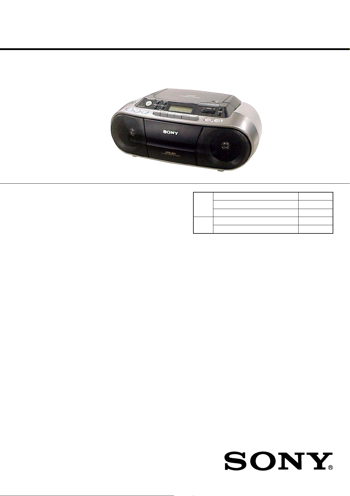
CFD-S01
SERVICE MANUAL
Ver. 1.0 2006.01
CD
Section
TC
Section
US Model
Model Name Using Similar Mechanism CFD-S350
CD Mechanism Type KSM-213CDP
Optical Pick-up Name KSS-213C
Model Name Using Similar Mechanism NEW
Tape Transport Mechanism Type MF-S01
SPECIFICATIONS
AUDIO POWER SPECIFICATIONS
POWER OUTPUT AND TOTAL HARMONIC DISTORTION
With 4-ohm loads, both channels driven from 150 -10,000 Hz; rated
1 W per channel-minimum RMS power, with no more than 10 % total
harmonic distortion in AC operation.
Other specifications
CD player section
System
Compact disc digital audio system
Laser diode properties
Emission duration: Continuous
Laser output: Less than 44.6 µW
(This output is the value measured at a distance of
about 200 mm from the objective lens surface on the
optical pick-up block with 7 mm aperture.)
Number of channels
2
Frequency response
20 - 20 000 Hz +1/–2 dB
Wow and flutter
Below measurable limit
Radio section
Frequency range
FM: 87.5 - 108 MHz
AM:530 - 1 710 kHz
IF
FM: 10.7 MHz
AM: 450 kHz
Antennas
FM: Telescopic antenna
AM: Built-in ferrite bar antenna
Cassette-corder section
Recording system
4-track 2 channel stereo
Fast winding time
Approx. 150 s (sec.) with Sony cassette C-60
Frequency response
TYPE I (normal): 80 - 10 000 Hz
General
Speaker
Full range: 8 cm dia., 4 Ω, cone type (2)
Outputs
Headphones jack (stereo minijack):
For 16 - 32 Ω impedance headphones
Power output
1.7 W + 1.7 W (at 4 Ω, 10% harmonic distortion)
Power requirements
For CD radio cassette-corder:
120 V AC, 60Hz
9 V DC, 6 R14 (size C) batteries
Power consumption
AC 13 W
– Continued on next page –
9-887-035-01
2006A04-1
© 2006.01
CD RADIO CASSETTE-CORDER
Sony Corporation
Personal Audio Division
Published by Sony Techno Create Corporation
Page 2
CFD-S01
r
Battery life
For CD radio cassette-corder:
FM recording
Sony R14P: approx. 6 h
Sony alkaline LR14: approx. 20 h
Tape playback
Sony R14P: approx. 3 h
Sony alkaline LR14: approx. 12 h
CD playback
Sony R14P: approx. 1.5 h
Sony alkaline LR14: approx. 7 h
Dimensions
Approx. 360 × 141 × 235 mm (w/h/d)
14 1/4 × 5 5/8 × 9 3/8 inches)
(incl. projecting parts)
Mass
Approx. 2.6 kg (5 lb, 11 oz) (incl. batteries)
Supplied accessory
AC power cord (1)
Design and specifications are subject to change
without notice.
SAFETY CHECK-OUT
After correcting the original service problem, perform the following
safety check before releasing the set to the customer:
Check the antenna terminals, metal trim, “metallized” knobs, screws,
and all other exposed metal parts for AC leakage.
Check leakage as described below.
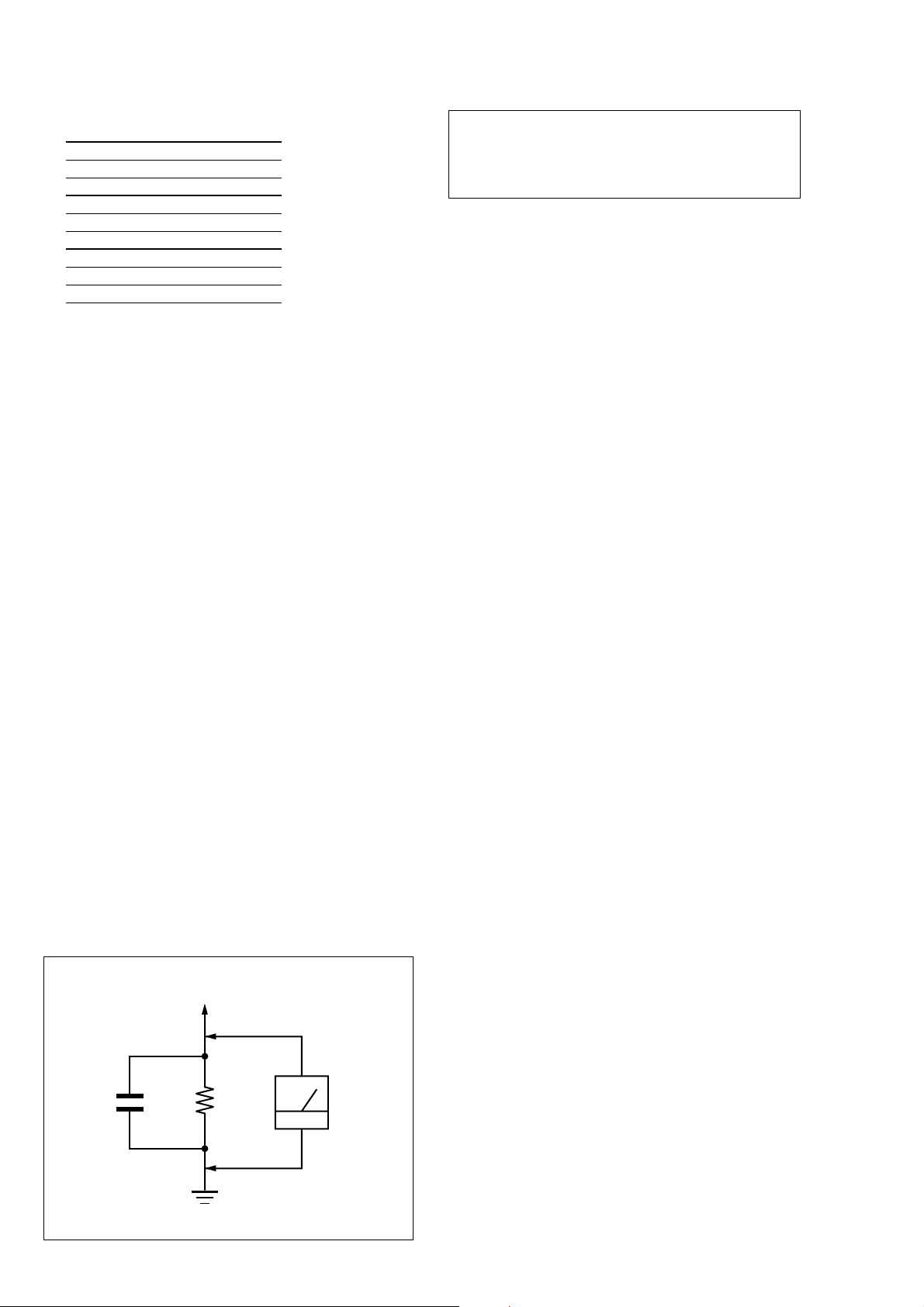
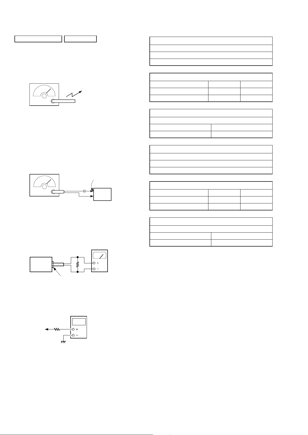
LEAKAGE TEST
The AC leakage from any exposed metal part to earth ground and
from all exposed metal parts to any exposed metal part having a
return to chassis, must not exceed 0.5 mA (500 microampers.).
Leakage current can be measured by any one of three methods.
1. A commercial leakage tester, such as the Simpson 229 or RCA
WT-540A. Follow the manufacturers’ instructions to use these
instruments.
2. A battery-operated AC milliammeter. The Data Precision 245
digital multimeter is suitable for this job.
3. Measuring the voltage drop across a resistor by means of a
VOM or battery-operated AC voltmeter. The “limit” indication is 0.75 V, so analog meters must have an accurate lowvoltage scale. The Simpson 250 and Sanwa SH-63Trd are
examples of a passive VOM that is suitable. Nearly all battery
operated digital multimeters that have a 2 V AC range are
suitable. (See Fig. A)
CAUTION
Use of controls or adjustments or performance of procedures
other than those specified herein may result in hazardous
radiation exposure.
Flexible Circuit Board Repairing
• Keep the temperature of the soldering iron around 270˚C during
repairing.
• Do not touch the soldering iron on the same conductor of the
circuit board (within 3 times).
• Be careful not to apply force on the conductor when soldering or
unsoldering.
Notes on Chip Component Replacement
• Never reuse a disconnected chip component.
• Notice that the minus side of a tantalum capacitor may be damaged
by heat.
NOTES ON HANDLING THE OPTICAL PICK-UP BLOCK
OR BASE UNIT
The laser diode in the optical pick-up block may suffer electrostatic
breakdown because of the potential difference generated by the
charged electrostatic load, etc. on clothing and the human body.
During repair, pay attention to electrostatic breakdown and also use
the procedure in the printed matter which is included in the repair
parts.
The flexible board is easily damaged and should be handled with
care.
NOTES ON LASER DIODE EMISSION CHECK
The laser beam on this model is concentrated so as to be focused on
the disc reflective surface by the objective lens in the optical pickup block. Therefore, when checking the laser diode emission,
observe from more than 30 cm away from the objective lens.
Notes on DualDiscs
A DualDisc is a two sided disc product which mates DVD recorded
material on one side with digital audio material on the other side.
However, since the audio material side does not conform to the
Compact Disc (CD) standard, playback on this product is not
guaranteed.
To Exposed Metal
Parts on Set
AC
0.15 µF
1.5 k
Ω
Earth Ground
voltmete
(0.75 V)
Fig. A. Using an AC voltmeter to check AC leakage.
2
SAFETY-RELATED COMPONENT WARNING!!
COMPONENTS IDENTIFIED BY MARK 0 OR DOTTED LINE
WITH MARK 0 ON THE SCHEMATIC DIAGRAMS AND IN
THE PARTS LIST ARE CRITICAL TO SAFE OPERATION.
REPLACE THESE COMPONENTS WITH SONY PARTS WHOSE
PART NUMBERS APPEAR AS SHOWN IN THIS MANUAL OR
IN SUPPLEMENTS PUBLISHED BY SONY.
Page 3

CFD-S01
UNLEADED SOLDER
•
Boards requiring use of unleaded solder are printed with the leadfree mark (LF) indicating the solder contains no lead.
(Caution: Some printed circuit boards may not come printed with
the lead free mark due to their particular size.)
: LEAD FREE MARK
Unleaded solder has the following characteristics.
• Unleaded solder melts at a temperature about 40°C higher than
ordinary solder.
Ordinary soldering irons can be used but the iron tip has to be
applied to the solder joint for a slightly longer time.
Soldering irons using a temperature regulator should be set to
about 350°C.
Caution: The printed pattern (copper foil) may peel away if the
heated tip is applied for too long, so be careful!
• Strong viscosity
Unleaded solder is more viscous (sticky, less prone to flow)
than ordinary solder so use caution not to let solder bridges
occur such as on IC pins, etc.
• Usable with ordinary solder
It is best to use only unleaded solder but unleaded solder may
also be added to ordinary solder.
TABLE OF CONTENTS
1. SERVICING NOTES ................................................ 4
2. GENERAL ................................................................... 5
3. DISASSEMBLY
3-1. Cabinet (Rear) Assy ......................................................... 7
3-2. Cabinet (Front) Assy, Cabinet (Upper) Assy ................... 7
3-3. Main Board ...................................................................... 8
3-4. CD Block Assy ................................................................ 8
3-5. CD Motor Board.............................................................. 9
3-6. Optical Pick-up................................................................ 9
3-7. Control Board .................................................................. 10
3-8. CD Lid ............................................................................. 10
3-9. Tape Mechanism Block, Belt (1), Belt (2) ...................... 11
3-10. TC Board ......................................................................... 11
3-11. Key (FUNC) Board, Key (VOL) Board .......................... 12
3-12. Power Board .................................................................... 12
4. MECHANICAL ADJUSTMENTS......................... 13
5. ELECTRICAL ADJUSTMENTS
Tape Section .................................................................... 13
Tuner Section................................................................... 14
CD Section ...................................................................... 16
6. DIAGRAMS
6-1. Block Diagram – CD Section – ....................................... 17
6-2. Block Diagram – Main Section – .................................... 18
6-3. Circuit Boards Location .................................................. 19
6-4. Schematic Diagram – Main Section (1/4) – .................... 20
6-5. Schematic Diagram – Main Section (2/4) – .................... 21
6-6. Schematic Diagram – Main Section (3/4) – .................... 22
6-7. Schematic Diagram – Main Section (4/4) – .................... 23
6-8. Printed Wiring Board – Main Section – .......................... 24
6-9. Printed Wiring Boards – TC Section – ............................ 25
6-10. Schematic Diagram – TC Section – ................................ 26
6-11. Printed Wiring Boards – Control Section – ..................... 27
6-12. Schematic Diagram – Control Section – ......................... 28
6-13. Printed Wiring Boards – Power Supply Section – ........... 29
6-14. Schematic Diagram – Power Supply Section – ............... 30
7. EXPLODED VIEWS
7-1. Rear Cabinet Section ....................................................... 38
7-2. Front Cabinet Section (1) ................................................ 39
7-3. Front Cabinet Section (2) ................................................ 40
7-4. Upper Cabinet Section (1) ............................................... 41
7-5. Upper Cabinet Section (2) ............................................... 42
7-6. CD Mechanism Section ................................................... 43
8. ELECTRICAL PARTS LIST .................................. 44
3
Page 4
CFD-S01
SECTION 1
SERVICING NOTES
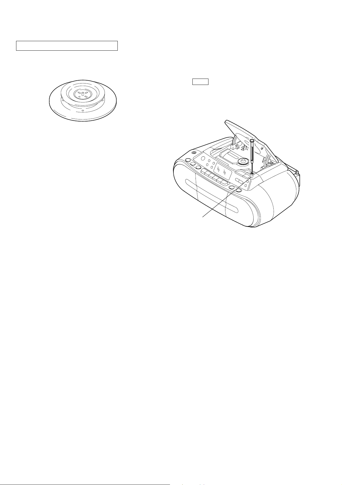
CHUCK PLATE JIG ON REPAIRING
On repairing CD section, playing a disc without the lid (CD), use
Chuck Plate Jig.
• Code number of Chuck Plate Jig: X-4918-255-1
LASER DIODE AND FOCUS SEARCH OPERATION
CHECK
1. Turn ON the [POWER] button and press [CD] button to CD
position.
2. Open the CD lid.
3. Turn on S801 with screwdriver, etc. as following figure.
4. Press the N X (CD) button.
5. Confirm the laser diode emission while observing the objecting
lens. When there is no emission, Auto Power Control circuit or
Optical Pick-up is broken.
Objective lens moves up and down three times for focus search.
S801
4
Page 5
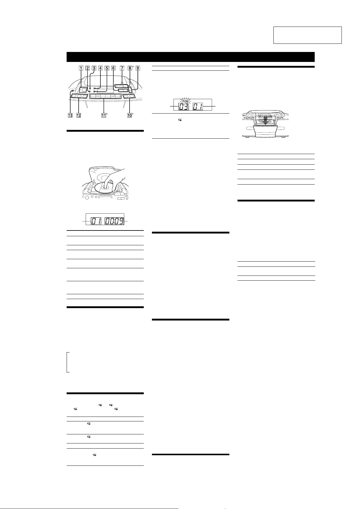
Basic Operations
*
VOLUME + 0 u 8, and n qa have a tactile dot.
Playing a CD
1
Press CD qs (direct power-on).
2
Press Z PUSH OPEN/CLOSE 7 and place a disc
with the label side up on the CD compartment.
To close the CD compartment, press Z PUSH OPEN/
7
.
CLOSE
3
Press u 8.
The player plays all the tracks once.
Track
number
To Press
Pause playback
Stop playback
Go to the next
track
Go back to the
previous track
Locate a point
while listening to
the sound
Locate a point
while observing
the display
Remove the CD
8. To resume play, press it
u
again.
8.
x
6.
>
6.
.
(forward) or . (backward)
>
6
while playing and hold it until
you find the point.
(forward) or . (backward)
>
6
in pause and hold it until you
find the point.
PUSH OPEN/CLOSE
Z
Using the display
To check the total track number and playing
time
Press DISPLAY•ENTER 5 in stop mode.
To check the remaining time
Press DISPLAY•ENTER 5 repeatedly while playing a
CD. The display changes as follows:
B
The current track number and playing time
r
The current track number and the remaining
time of the current track*
r
The number of tracks left and remaining
time on the CD
* For a track whose number is more than 20, the remaining time
appears as “- -:- -” in the display.
Selecting the play mode
Press MODE 4 until “ 1”, “ ”, “SHUF”, “SHUF”
and “
”, “PGM”, or “PGM” and “ ” appear in
the display. Then proceed as follows:
To Select Select Then do this
Repeat a
single track
Repeat all
tracks
Shuffle play “SHUF” Press
Repeat
tracks in
random
order
“ 1” Press . or > 6 to
select the track that you want
to repeat, then press
” Press u 8.
“
Press
“SHUF”
”
and “
u
u
8.
8.
Playing
time
7
u
8.
SECTION 2
GENERAL
To Select Select Then do this
Program
play
repeat
programed
tracks
To cancel selected play mode
Press MODE 4 repeatedly until the selected mode
disappears from the display.
To check the programed track and playing
order in the display
To check the order of tracks before play, press
DISPLAY•ENTER
Every time you press the button, the track number
appears in the programed order.
To change the current program
Press x 8 once if the CD is stopped and twice if the
CD is playing. The current program will be erased.
Then create a new program following the programing
procedure.
Tips
• You can play the same program again, since the program is saved
• You can record your own program. After you’ve created the
Listening to the radio
1
2
Tip
If the FM broadcast is noisy, press MODE 4 until “Mono” appears
in the display and radio will play in monaural.
Presetting radio stations
You can store radio stations into the player’s memory.
You can preset up to 30 radio stations, 20 for FM and 10
for AM in any order.
1
2
3
If a station cannot be preset automatically
You need to preset a station with a weak signal
manually.
1
2
3
4
5
Tip
The preset radio stations remain in memory even if you unplug the
AC power cord or remove the batteries.
Playing preset radio stations
1
2
“PGM” Press . or > 6 then
press DISPLAY•ENTER
5
for the tracks you want
to program in the order you
want up to 20 tracks. Then
press
8.
u
Programed
track
“PGM”
Press
and “
5
until you open the CD compartment.
program, insert a blank tape and press
Press RADIO BAND•AUTO PRESET qs
repeatedly (direct power-on).
Each time you press the button, the indication
changes as follows:
“FM” t “AM”
Hold down TUNE + or – 9 until the frequency
digits begin to change in the display.
The player automatically scans the radio frequencies
and stops when it finds a clear station.
If you can’t tune in a station, press the button
repeatedly to change the frequency step by step.
When an FM stereo broadcast is received, “ST”
appears.
Press RADIO BAND•AUTO PRESET qs to
select the band.
Hold down RADIO BAND•AUTO PRESET qs for
2 seconds until “AUTO” flashes in the display.
Press DISPLAY•ENTER 5.
The stations are stored in memory from the lower
frequencies to the higher ones.
Press RADIO BAND•AUTO PRESET qs to
select the band.
Tune in a station you want.
Hold down DISPLAY•ENTER 5 for 2 seconds
until the preset number flashes in the display.
Press PRESET + or – 6 until the preset number
you want for the station flashes in the display.
Press DISPLAY•ENTER 5.
The new station replaces the old one.
Press RADIO BAND•AUTO PRESET qs to
select the band.
Press PRESET + or – 6 to tune in the stored
station.
.
press DISPLAY•ENTER
”
5
for the tracks you want
to program in the order you
want up to 20 tracks. Then
Press
u
.
z
Playing
order
or > 6 then
8.
qa to start recording.
CFD-S01
This section is extracted
from instruction manual.
Playing a tape
1
Press TAPE qs (direct power-on).
2
Press xZ qa, and insert the tape into the tape
compartment with the side you want to play
facing you. Use TYPE I (normal) tape only. Close
the compartment.
Make sure there is no slack in the tape to avoid
damaging the tape or the unit.
3
Press n qa.
The player starts playing.
To Press
Pause playbackX qa. To resume play, press it again.
Stop playback
Fast-forward or
rewind*
Eject the cassette
* When the tape is wound to the end, press xZ qa to release m or
qa.
M
Recording on a tape
1
Press xZqa to open the tape compartment
and insert a blank tape with the side you want to
record on facing you. Use TYPE I (normal) tape
only. Close the compartment.
2
Select the program source you want to record.
To record from the CD player, place a CD and press
qs
CD
To record from the radio, tune in the station you want.
3
Press z qa to start recording
is depressed automatically).
(
n
To Pr ess
Pause recording
Stop recording
Tips
• Adjusting the volume or the audio emphasis will not affect the
recording level.
• For the best results, use wall outlet as a power source for recording.
• To erase a recording, proceed as follows:
1 Insert the tape whose recording you want to erase.
2 Press TAPE
3 Press
qa.
z
qa.
xZ
or M (fast forward or rewind)
m
qa
.
qa.
xZ
.
X
press it again.
xZ
qs
.
qa. To resume recording,
qa
.
5
Page 6
CFD-S01
SECTION 3
DISASSEMBLY
Note: This set can be disassemble according to the following sequence.
SET
3-1. CABINET (REAR) ASSY
(Page 7)
3-2. CABINET (FRONT) ASSY,
CABINET (UPPER) ASSY
(Page 7)
3-3. MAIN BOARD
(Page 8)
3-4. CD BLOCK ASSY
(Page 8)
3-9. TAPE MECHANISM BLOCK,
3-12. POWER BOARD
(Page 12)
BELT (1), BELT (2)
(Page 11)
3-7. CONTROL BOARD
(Page 10)
3-11. KEY (FUNC) BOARD,
KEY (VOL) BOARD
(Page 12)
3-10. TC BOARD
(Page 11)
3-8. CD LID
(Page 10)
3-5. CD MOTOR BOARD
(Page 9)
3-6. OPTICAL PICK-UP
(Page 9)
6
Page 7
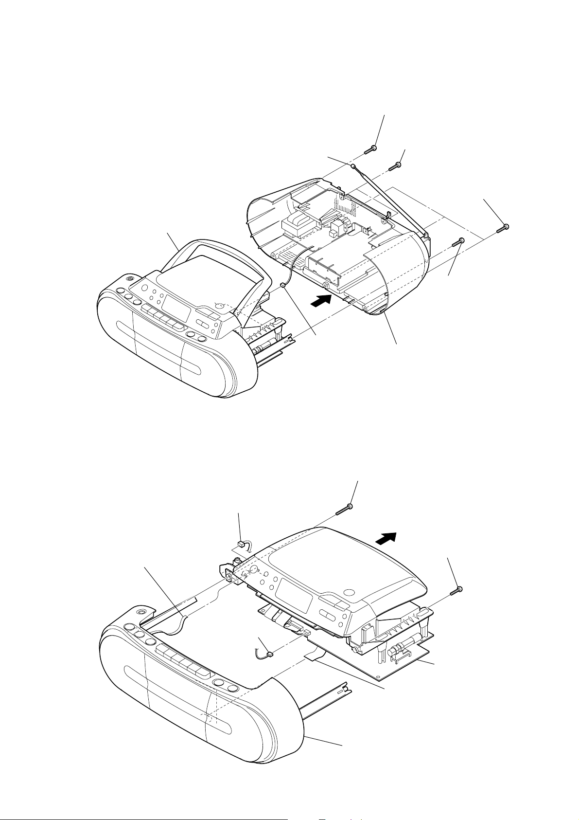
Note: Follow the disassembly procedure in the numerical order given.
)
3-1. CABINET (REAR) ASSY
telescopic antenna
handle
5
2
screw
(+BV tapping B2.6)
1
two
screws
(+BV tapping (B2.6))
4
three
(+BV tapping (B2.6))
3
(+BV tapping B2.6)
CFD-S01
screws
screw
6
3-2. CABINET (FRONT) ASSY, CABINET (UPPER) ASSY
1
CN308 (4P)
5
flexible flat cable (4 core)
(CN402)
6
CN304 (4P)
CN305 (3P)
2
(+BV tapping B2.6)
screw
7
cabinet (rear) assy
4
3
(+BV tapping B2.6
screw
7
flexible flat cable (11 core)
(CN301)
8
cabinet (front) assy
9
cabinet (upper) assy
7
Page 8
CFD-S01
)
)
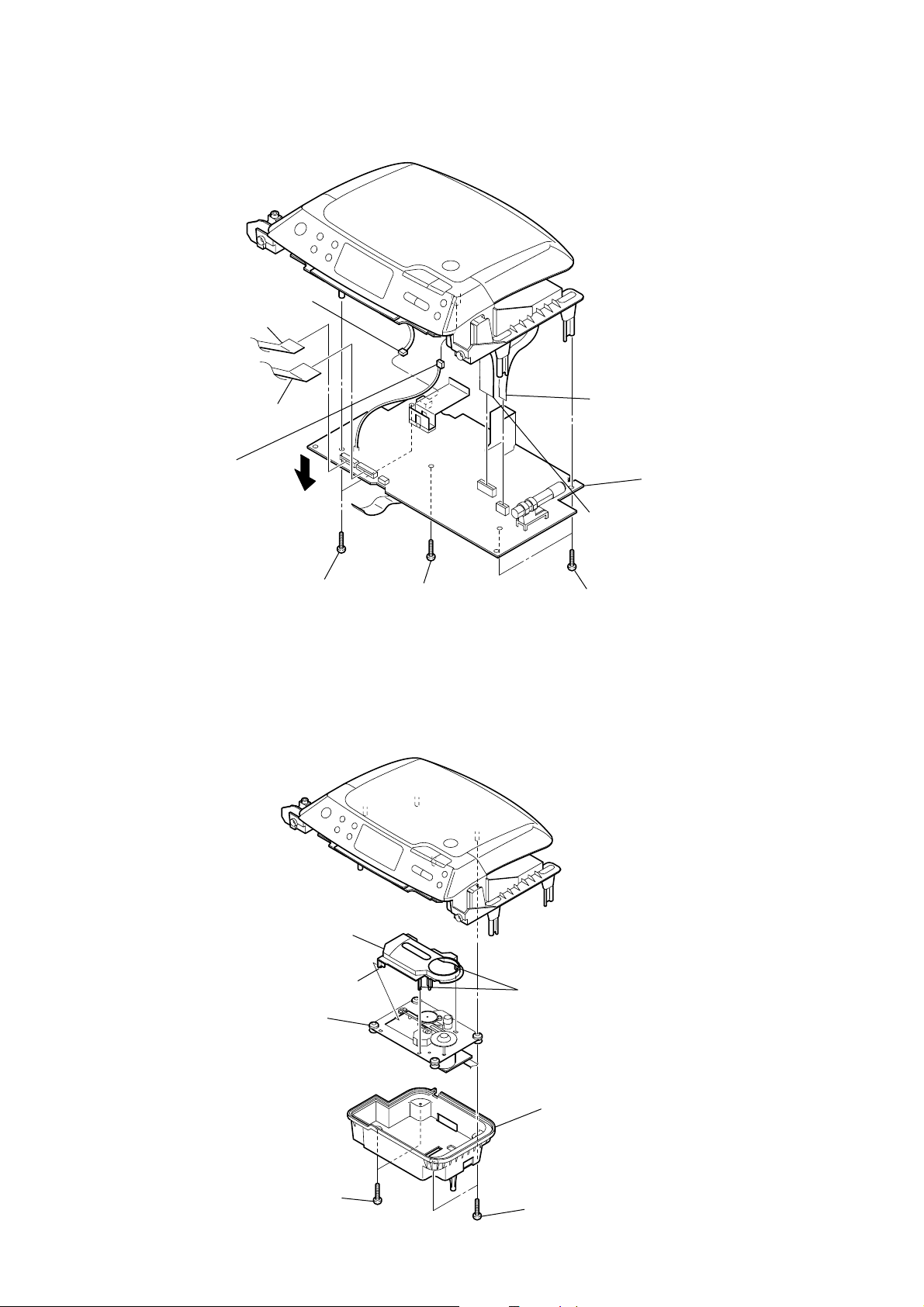
3-3. MAIN BOARD
3
flexible flat cable (12 core)
(CN802)
2
flexible flat cable (14 core)
(CN801)
0
connector
(S801)
1
CN306 (4P)
7
8
flexible flat cable (6 core)
(CN702)
qa
MAIN board
9
flexible flat cable (16 core
(CN701)
3-4. CD BLOCK ASSY
6
two
(+BV tapping B2.6)
4
CD cover
5
CD block assy
screws
claw
5
screw
(+BV tapping B2.6)
two claws
4
two
screws
(+BV tapping B2.6)
3
CD chassis
2
two
screws
(+BV tapping (B2.6))
1
two
screws
(+BV tapping (B2.6)
8
Page 9
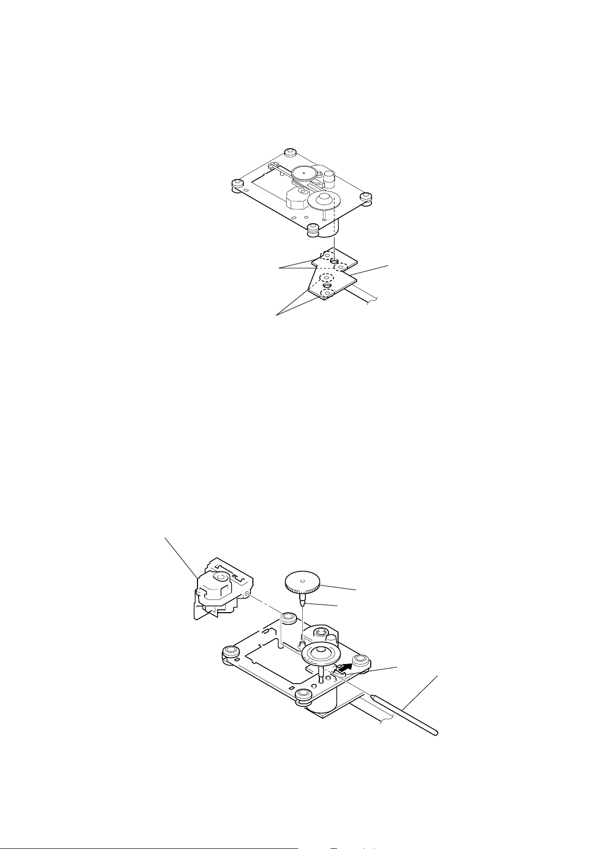
3-5. CD MOTOR BOARD
d
t
2
Remove the two solders.
3
CD MOTOR boar
CFD-S01
3-6. OPTICAL PICK-UP
5
optical pick-up
1
Remove the two solders.
claw
1
gear (A)
3
2
claw
sled shaf
4
9
Page 10
CFD-S01
d
g
3-7. CONTROL BOARD
3
CONTROL boar
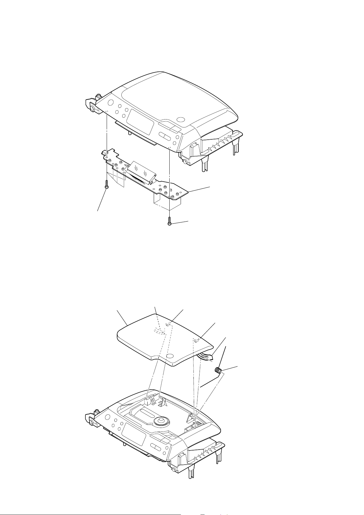
3-8. CD LID
2
five
screws
(+P tapping (B2.6))
5
CD lid
1
1
four
screws
(+P tapping (B2.6))
2
4
3
6
CD sprin
10
Page 11
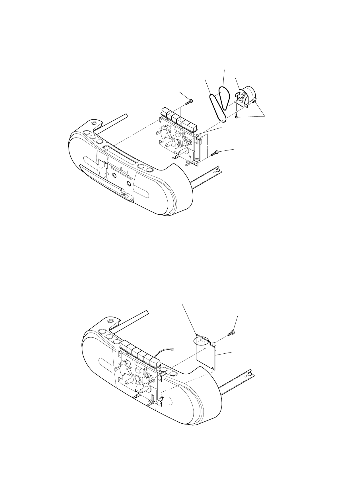
3-9. TAPE MECHANISM BLOCK, BELT (1), BELT (2)
1
two
screws
(+BV tapping (B2.6))
7
belt (2)
6
belt (1)
5
motor bracket
3
tape mechanism block
2
two
screws
(+BV tapping (B2.6))
4
two screws
CFD-S01
3-10. TC BOARD
2
Remove the four solders.
1
screw
(+P tapping (B2.6))
3
TC board
11
Page 12
CFD-S01
s
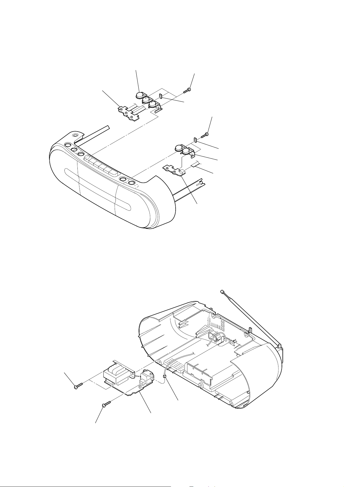
3-11. KEY (FUNC) BOARD, KEY (VOL) BOARD
9
8
KEY (FUNC) board
button (FUNC)
6
three
(+BV tapping (B2.6))
7
RETAINER board
screws
2
two
(+BV tapping (B2.6))
3
5
1
flexible flat cable (4 core)
(CN401)
screws
two RETAINER board
button (volume)
3-12. POWER BOARD
3
two
screws
(+BV tapping (B2.6))
4
KEY (VOL) board
12
2
screw
(+BV tapping (B2.6))
4
POWER board
1
CN902 (2P)
Page 13
SECTION 4
MECHANICAL ADJUSTMENTS
CFD-S01
SECTION 5
ELECTRICAL ADJUSTMENTS
PRECAUTION
1. Clean the following parts with a denatured-alcohol-moistened
swab :
record/playback head pinch roller
erase head rubber belts
capstan idlers
2. Demagnetize the record/playback head with a head demagnetizer.
(Do not bring the head magnetizer close to the erase head.)
3. Do not use a magnetized screwdriver for the adjustments.
4. The adjustments should be performed with the rated power
supply voltage (9V) unless otherwise noted.
Torque Measurement
Mode Torque meter Meter reading
2.95 – 6.86 mN • m
FWD CQ-102C (30 – 70 g • cm)
(0.42 – 0.97 oz • inch)
FWD
Back Tension
FF CQ-201B (more than 60 g • cm)
REW CQ-201B (more than 60 g • cm)
CQ-102C (1.5 – 5.5 g • cm)
0.15 – 0.53 mN • m
(0.021 – 0.076 oz • inch)
more than 5.88 mN • m
(more than 0.83 oz • inch)
more than 5.88 mN • m
(more than 0.83 oz • inch)
TAPE SECTION 0 dB = 0.775 V
• Standard Output Level
Output terminal HP OUT
load impedance 32 Ω
output signal level 0.25 V (–10 dB)
• Test Tape
Type Signal Used for
WS-48A 3 kHz, 0 dB tape speed adjustment
Tape Speed Adjustment
Procedure:
Mode: playback
test tape
WS-48A
(3 kHz, 0 dB)
set
i
jack (J321)
Adjust so that the value on the digital frequency counter is
3,000 Hz.
digital frequency
counter
Ω
32
Tape Tension Measurement
Mode Tension meter Meter reading
FWD CQ-403A
more than 100 g
(more than 3.53 oz)
Specification Value:
Digital frequency counter
2,910 to 3,090 Hz
Adjust so that the frequency at the beginning and that at the end of
tape winding are between 2,910 to 3,090 Hz.
Adjustment Location:
Tape speed adjustment
control inside motor
13
Page 14
CFD-S01
)
TUNER SECTION 0 dB = 1 µV
• AM Section
Setting:
RADIO BAND•AUTO PRESET button: AM
AM RF signal
generator
30% amplitude
modulation by
400 Hz signal
• FM Section
Setting:
RADIO BAND•AUTO PRESET button: FM
FM RF signal
generator
75 kHz frequency
deviation by 1 kHz signal
output level : as low as possible
Put the lead-wire
antenna close to
the set.
0.01
µ
F
ANT2
set
AM IF ADJUSTMENT
Adjust for a maximum reading on level meter.
T1
450 kHz
AM FREQUENCY COVERAGE CHECK
Frequency Display 530 kHz 1,710 kHz
Reading on Digital voltmeter 0.8 ± 0.3 V 5.8 ± 0.1 V
Adjustment Part L3 <confirmation>
AM TRACKING ADJUSTMENT
Adjust for a maximum reading on level meter.
ANT1 CT3
620 kHz 1,400 kHz
FM IF ADJUSTMENT
Adjust for a maximum reading on level meter.
L6
10.7 MHz
FM FREQUENCY COVERAGE ADJUSTMENT
Frequency Display 87.5 MHz 108 MHz
Reading on Digital voltmeter 1.5 ± 0.3 V 3.0 ± 0.2 V
Adjustment Part <confirmation> L2
• Connecting Level Meter (FM, AM)
level meter
(range: 0.5–5 V ac
32
Ω
set
i
jack (J321)
• Connecting Digital Voltmeter (FM, AM)
digital
voltmeter
Ω
100 k
TP (VT)
•Repeat the procedures in each adjustment several times, and the
frequency coverage and tracking adjustments should be finally
done by the trimmer capacitors.
FM TRACKING ADJUSTMENT
Adjust for a maximum reading on level meter.
L1 CT1
87.5 MHz 108 MHz
Adjustment Location: See page 15.
14
Page 15
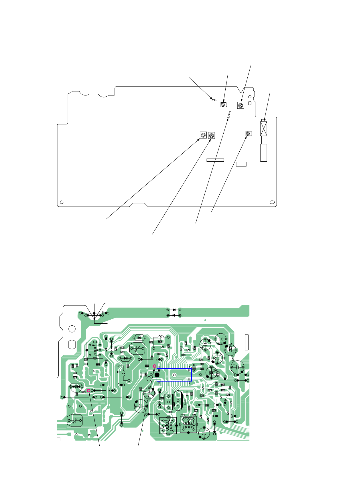
Adjustment Location:
E
– MAIN BOARD (Component Side) –
L2: FM FREQUENCY COVERAGE
ADJUSTMENT
CFD-S01
L3: AM FREQUENCY COVERAG
ADJUSTMENT
CT1: FM TRACKING
ADJUSTMENT
ANT1: AM TRACKING
ADJUSTMENT
CN701
CN702
Test Point:
L6: FM IF ADJUSTMENT
T1: AM IF ADJUSTMENT
– MAIN BOARD (Conductor Side) –
JW232
JW231
L3
C14
C11
C10
C13
C12
R6
D3
C9
R5
JW226
CT3
C15
JW218
JW224
JW217
JW219
ANT2
R11
JW223
C3
C2
R2
R1
D1
C1
L1
JW220
CT3: AM TRACKING ADJUSTMENT
L1: FM TRACKING ADJUSTMENT
D5
D4
D2
CT1
C21
C70
C29
JW207
C67
C22
C23
C6
C4
R26
JW209
T1
L2
R3
JW208
C17
C18
R18
C37
C46
C40
C35
C38
R22
JW189
JW191
R14
C43
R24
C20
C326
D6
JW183
JW184
JW187
C36
R21
R899
R23
JW190
C5
C7
C24
C16
R4
R13
R9
R7
R12
X1
IC1
CF2
CF3
C25
C27
C26
R25
C28
R29
L6
R28
C42
JW188
R41
C19
C45
R15
R39
R27
C41
C39
R20
C34
R19
C32
R17
R10
R16
C30
TP (VT) TP (GND)
15
Page 16
CFD-S01
C782
R715
CD SECTION
CD section adjustments are done automatically in this set.
In case of operation check, confirm that focus bias.
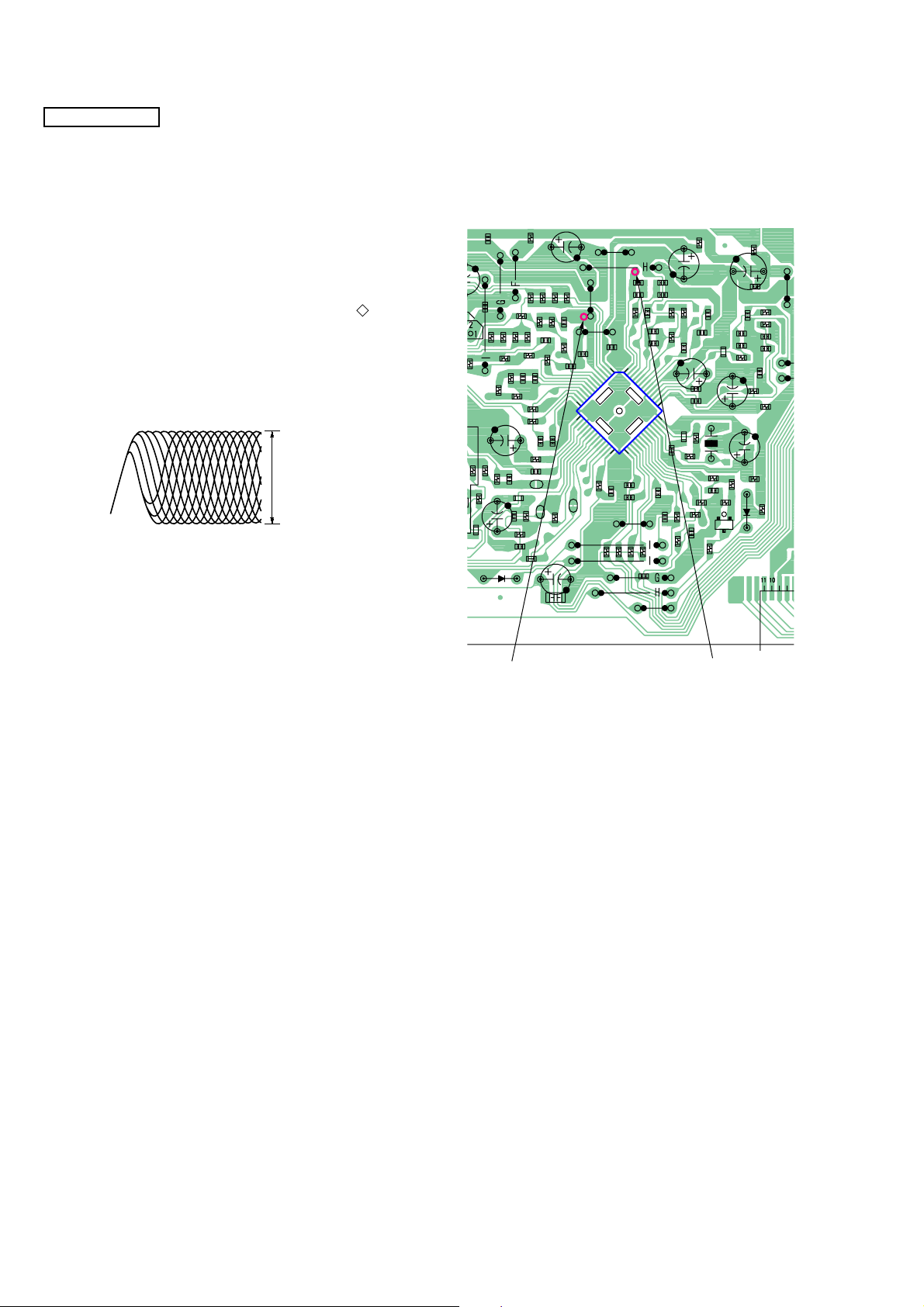
FOCUS BIAS CHECK
1. Connect the oscilloscope between IC701 pin ts and pin 4 (or
TP (RF) and TP (VREF)).
2. Insert the disc (PATD-012 (Tr 15)). (Part No. : 4-225-203-01)
3. Press the N X (CD) button.
4. Confirm that the oscilloscope waveform is as shown in the figure
below. (eye pattern)
A good eye pattern means that the diamond shape ( ) in the
center of the waveform can be clearly distinguished.
• RF signal reference waveform (eye pattern)
VOLT/DIV : 50 mV (10 : 1 probe in use)
TIME/DIV : 500 nS
RF level :
1.7
±
0.2 Vp-p
When observing the eye pattern, set the oscilloscope for AC range
and raise vertical sensitivity.
Test Point:
– MAIN BOARD (Conductor Side) –
R721
C703
C772
JW204
R782
JC704
R702
R725
JW205
R781
R783
D703
C706
JW203
R701
R714
C716
R728
C720
JW202
R704
R726
C719
JC702
R700
R712
R710
C774
R703
C718
R708
C777
JC703
R740
C709
R717
R722
C712
R736
R707
R716
C710
R727
C717
TP701
JW197
JW198
C748
C707
R705
R713
TP702
R711
C711
C713
R734
R706
C700
R709
14
C708
C759
JW195
TP703
R757
JW193
JW194
R754
JW192
C705
26
R758
JW200
C755
C779
113
C725
RF
R772
C762
C754
C753
52
IC701
27 39
C726
C727
JW196
R755
R759
C728
JW199
JW201
C757
C729
C730
R766
40
C758
R768
C704
C744
C745
C738
R762
R756
C749
JC705
R748
R760
R770
C752
C773
R763
C731
R761
X701
R739
FB704
C751
R746
C750
JC701
R743
E CB
Q703
C747
C764
C763
R773
FB701
C761
R742
C735
FB702
C767
R774
D704
C766
C733
R775
R776
C769
C765
FB703
R744
JW180
FFC
TP (VREF)
TP (RF)
16
Page 17

SECTION 6
DIAGRAMS
6-1. BLOCK DIAGRAM — CD SECTION —
CFD-S01
A
C
B
D
E
F
LD
PD
OPTICAL PICK-UP
BLOCK
(KSS-213C)
TRACKING
COIL
FOCUS
COIL
M702
SLED
MOTOR
M701
SPINDLE
MOTOR
(LIMIT)
VC
S701
S801
PUSH
OPEN/
CLOSE
8FS
DOUT (O)
BUSY (O)
C-DOUT
CD-BUSY
DIGITAL
FILTER
&
1-bit DAC
GENERATOR
XI (I)
16.93MHz
U-COM
(VDD)
A
C
B
D
E
F
LD
PD
VR
VC
T+
T–
F+
F–
M
M
LD POWER
CONTROLLER
Q701
SL+
SL–
SP+
SP–
VC
Signal path
: CD
AC (I)
2
BD (I)
3
E (I)
5
F (I)
6
LD (O)
12
PD (I)
11
4
VBIAS (O)
12
11
17
18
26
27
2
1
(Page 18)
APC
T+
TRACKING
COIL
T–
DRIVE
F+
FOCUS
COIL
F–
DRIVE
SL–
SLED
MOTOR
SL+
DRIVE
SP+
SPINDLE
MOTOR
SP–
DRIVE
SLED/SPINDLE
MOTOR DRIVER,
TRACKING/FOCUS
COIL DRIVER
IC703
CD-LIM_SW
64
CD DOOR
29
CD 3.3V
CD-CONT
B
PRI-
SERVO
AMP
42
3V-CHK
TIN
(FIN)
MUTE
(SLIN)
SPIN
OPOUT
OPIN
VREF
Q957-959,D957
9
20
7
24
3
14
15
23
CD +3.3V
REC/PB
POWER
CONTROL
CONTROL
JUMPO (O)
18
VC
CD 6V
TAPE 6V
RADIO 6V
DIGITAL
SERVO
SDOUT (O)
21 22
CLVOUT(O)
41
+
6V-CHK
39
SYNCHRONOUS
CIRCUIT
BATT-CHK-H
SYSTEM SERVO PROCESSOR,
DIGITAL SIGNAL PROCESSOR
ERROR
AMP
Q705
ERROR
AMP
Q704
SYSTEM CONTROLLER
IC801 (1/2)
RIPPLE
FILTER
Q304
9V (SW)
R-VT
D324
RF AMP,
IC701
PULSE/DC
CONVERTER
Q703
P-CON
65
D951
D952
DIN (I)
RESETX (I)
MONI1
XPLCK
35 34 31 2826 30 27 37 3832 29
D703
POWER
SWITCH
Q951
+3.3V REG
IC802
AUDIO+6V
REG
Q955,D953
POWER
SWITCH
Q952,953
3.3V
SUBSYQ (O)
51
CD-RESETX
CD-SUBSYQ
23
54 62 55 52 5364
CD-DIN
DSP
I/F
R/W (I)
MCK (I)
CD-R/W
VDD
CD-MCK
LDACO (O)
CLOCK
XO (O)
X701
41
RDA
43
D901 – 904
RECT
BATT
F902
CD_IN_ L
CD_IN_R
T901
POWER
TRANSFORMER
DRY BATTERY
(IEC DESIGNATION R20)
6PCS, 9V
SIZE "D"
A
(Page 18)
J901
AC IN
CFD-S01
17 17
Page 18

CFD-S01
6-2. BLOCK DIAGRAM — MAIN SECTION —
HRP301
RECORD/PLAYBACK
HEAD
L-CH
R-CH
HE301
ERASE HEAD
(Page 17)
S301
(REC/PB)
REC
PB
A
AUDIO 6V
CD_IN_R
CD_IN_L
-1 -2
27
SAD
EEPROM
IC805
TAPE REC
SCL
7980
65
S1
COM1|COM4
10–266 – 9
LIQUID CRYSTAL
DISPLAY PANEL
LCD401
R.RO
9
R.IN
8
14
4
24
5
6
R.LIN
L.RO
L.LIN
L.IN
REF
T301
DET
REC
21 22 16
REC BIAS OSC
Q301
ALC 2
RADIO L
L.RAD
TU_IN_L
REC/PB
PRE AMP
IC301
R.RAD
TU_IN_R
L.LO
R.LO
LINE
TAPE
20
R-CH
18
17
15
TAPE
CD
CD-CONT
8 7
B
(Page 17)
37
SYSTEM CONTROLLER
IC801 (2/2)
|
S17
XT171XT2
70
X801
32.768kHz
74X175
X802
4.19MHz
X2
76
1
RESET
IC804
2
3.3V
RST
FUNC TC
FUNC CD
TU-DATA
57 58 5956
TU-COUNT
TU-CLK
TU-CE
IC302
ELECTRONIC VOLUME
L-IN
VOL AMP
LOGIC
CLK4DATA
5
7736 78
V-CLK
V-DATA
L-OUT
MEGA
BASS
SWITCH
Q122
68
50
D322
DBB
WP/INI
Q805, D801, 804
MUTE
Q124
35
49
A-MUTE
TC-PLAY
POWER AMP
IC303
6 2
U-COM
(VDD)
LEVEL
DETECT
D323
TAPE PLAY
DETECT
Q808
KEY145KEY244KEY3
43
9V (SW)
R-CH
OPR/BATT
D406
9V (SW)
SP101
SPEAKER
(L-CH)
SP201
SPEAKER
(R-CH)
S301
(TAPE PLAY)
M
M301
CAPSTAN/REEL
MOTOR
J321
i
ANT2
FM
TELESCOPIC
ANTENNA
L3
AM
FREQUENCY
COVERAGE
CT3,ANT1
AM
TRACKING
D3
CT3
RADIO 6V
ANT1
AM
FERRITE-ROD
ANTENNA
L3
CT1,L1
FM
TRACKING
31
1
2
36
L1 CT1
RADIO 6V
AM OSC
AM RF-IN
REG
FM
RF-IN
(VT)
D1
AM
OSC
AM
MIX
FM
RF-OUT
28
FM
MIX
FM
OSC
3234
27PD26
LP-IN
LP-OUT
FM OSC
D2
RADIO 6V
R-VT
FM/AM RF AMP, MIX, OSC, IF AMP,
AM
MIX-OUT
FM
MIX-OUT
L2
FM MPX
IC1
T1
5 7
RADIO 6V
3
RADIO 6V
L2
FM
FREQUENCY
COVERAGE
CF2
CF3
MW
X1
75kHz
20 19 16 17CE15
X IN
X OUT
AM
IF-IN
FM
IF-IN
8
T1
IF
AM
DET
FM
DET
FM-DET
11
RADIO 6V
L6
AF
BUFFER
L6
FM
IF
DI
18
DO
CL
DET-OUT
23 22
MPX-IN
FM
MPX
R-OUT
L-OUT
TU_IN_R
13
12
KEY3
KEY2
KEY1
Signal path
: FM
: AM
: TAPE PLAY
: TAPE REC
: CD
R-ch is omitted due to same as
L-ch.
KEY NETWORK
S402,415,416,418
S401,403-405,410-412
S407,408,413,414,417
CFD-S01
1818
Page 19

THIS NOTE IS COMMON FOR PRINTED WIRING
d
d
BOARDS AND SCHEMATIC DIAGRAMS.
(In addition to this, the necessary note is
printed in each block.)
CFD-S01
6-3. CIRCUIT BOARDS LOCATION• NOTE FOR PRINTED WIRING BOARDS AND SCHEMATIC DIAGRAMS
POWER board
HEADPHONE board
CD MOTOR board
For schematic diagrams.
Note:
• All capacitors are in µF unless otherwise noted. (p: pF)
50 WV or less are not indicated except for electrolytics
and tantalums.
• All resistors are in Ω and 1/
specified.
• f : internal component.
• C : panel designation.
Note: The components identified by mark 0 or dotted line
with mark 0 are critical for safety.
Replace only with part number specified.
• A : B+ Line.
• H : adjustment for repair.
•Voltages and waveforms are dc with respect to ground
under no-signal (detuned) conditions.
– MAIN (1/4) Board –
no mark : CD PLAY
– MAIN (2/4) Board –
no mark : FM
(): AM
– MAIN (3/4), (4/4) and Other Boards –
no mark : FM
(): PB
<>: REC
[]: CD PLAY
•Voltages are taken with a VOM (Input impedance 10 MΩ).
Voltage variations may be noted due to normal production
tolerances.
•Waveforms are taken with a oscilloscope.
Voltage variations may be noted due to normal production
tolerances.
• Circled numbers refer to waveforms.
• Signal path.
F : FM
f : AM
E : PB
a : REC
J : CD PLAY
4
W or less unless otherwise
For printed wiring boards.
Note:
• X : parts extracted from the component side.
• Y : parts extracted from the conductor side.
• W : indicates side identified with part number.
f
•
• : Pattern from the side which enables seeing.
Caution:
Pattern face side: Parts on the pattern face side seen from
(Conductor Side) the pattern face are indicated.
Par ts face side: Parts on the parts face side seen from
(Component Side) the parts face are indicated.
: internal component.
(The other layers' patterns are not indicated.)
C
Q
B
E
Q
BCE
Q
B
C
These are omitted.
These are omitted.
E
KEY (FUNC) board
CONTROL board
TC board
• Waveforms
— MAIN Board —
1 IC701 9 (FEO (O))
– CD PLAY – – CD PLAY –
1.7V
Approx. 100mVp-p
100mV/div, 5msec/div
4 IC701 ts (EQO (O))
50mV/div, 0.5 µsec/div
BATTERY TERMINAL (R) boar
BATTERY TERMINAL (F) board
7 IC801 ug (X2)
1.7±0.2Vp-p
1V/div, 0.1 µsec/div
MAIN board
KEY (VOL) boar
3.5Vp-p
4.19MHz
CFD-S01
2 IC701 ek (XO (O))
– CD PLAY –
3.3Vp-p
16.93MHz
1V/div, 20nsec/div
3 IC701 rk (TEO (O))
– CD PLAY –
1.7V
Approx. 100mVp-p
100mV/div, 5msec/div
5 IC1 w; (X OUT)
75kHz
1V/div, 5 µsec/div
6 IC801 ua (XT2)
32.768kHz
1V/div, 10 µsec/div
2.0Vp-p
3.4Vp-p
— TC Board — (TAPE REC)
1
Q301 C (REC)
21.1 µsec
1V/div, 10 µsec/div
2
HRP301 (YEL)
21.1 µsec
10V/div, 10 µsec/div
2.8Vp-p
30Vp-p
19 19
Page 20

CFD-S01
6-4. SCHEMATIC DIAGRAM — MAIN SECTION (1/4) —
Q701
R716
CN701
C700
R700
R701
R702
R704
R703
R711
R726
• Refer to page 19 for Waveforms. • Refer to page 32 for IC Block Diagram. • Refer to page 34 for IC Pin Description of IC701.
C762
C753
R772
Q703
R743
R770
C754
R768
R742 R739
C773
C752
R766
IC701
C749
JC701
C744
R773
R774
C747
C745
R761
R756
R760
R755
X701
C764
C763
R762
C766
C765
R748
R763
C767
C769
R775
R776
JC705
C738
C733
D703
R759
R758
R757
R724
R719
R714
R710
C710
C777
R725
R715
R712
R717
R708
R707
R706
R705
C709
C701
C702
C772
C703
R721
R709
C759
R723
R722
C748
C707
C708
C751
C704
C750
C757
C758
C705
D704
C706
R713
C711
C712
C713
R746
FB704
R744
C755 C779
FB703
FB702
R778
C761
FB701
C735
(Page 22)
R777
M702
S701
FFC020
CN702
R749
R750
Q705
R785 R783
R784
C783
Q704
R745
C782
IC703
R782
R781
C774
R780
R747
C781
R729
R728
C723
R751
C717
R786
C716
R730
R731
JC703JC704
R727
TP701
R733
R732
R736
C718 R740
C719
C720
TP704
TP702
R734
IC B/D
R741
TP703
JC702
R754
C725
C730
C731
C729
C728
C727
C726
CFD-S01
M701
C721 C760
C722
2020
Page 21

CFD-S01
6-5. SCHEMATIC DIAGRAM — MAIN SECTION (2/4) —
L3
R1 R2
C13
C14
C10
D3
C12
C11
C15
R6
C9
R5
D1
CT1
L1 L2 R3
C7
• Refer to page 19 for Waveforms. • Refer to page 31 for IC Block Diagram.
R11
C2
C16
C4C67
C3
R7
D2
R9
C5
C6
IC B/D
R4
C45
R13
R12
R14
C17
C19
C18
R27
C20C46
C39
C40
R15R39
C41
C42C1
X1
C43
R24
D6
ANT2
ANT1
CT3
C25
C22
C21
C29
R26
D4
D5
C70
C23
C24
T1
CF3
CF2
C26
IC1
R28
R25
C27
C28
C30
R10
R41
R29
L6
C31 C33
C34C32
R19R18 R21R20
C35 C36 C37
R16
R17
C38
R22
R23
(Page 22)
CFD-S01
21 21
Page 22

CFD-S01
6-6. SCHEMATIC DIAGRAM — MAIN SECTION (3/4) —
FFC11P
(Page 26)
• Refer to page 19 for Waveforms. • Refer to page 36 for IC Pin Description of IC801.
R844
R847
R870
R871
R872
R873
R874
R875
R876
R877
R878
R879
R880
R881
R882
R883
R884
R846
IC801
R801
C351
C352
R837
R803
R864
R863
R890
R889
R888
R887
R886
R804
R862
R901
R903
R905
R885
R848
R807
R895
R854
X801
R896
R869
R322
R834
R833
R832
R843
R842
X802
C815
C814
R836
C824
IC805
R860
R845
C821C801
R853 R856
R850
R852R851
R849
C822
IC804
L802
L801
CN801
(Page 28)
C820
CN802
(Page 28)
(Page 23)
C826
C817
IC802
C816
R861
R802
R835
C835
R840
JC801
D804
R823
R824
R808
R827
D801
JC802
C802
R894
R891
R893
R829
Q805
R892
R858
R805
R806
R857
R868
R825
R838
R826
R841
R828
R818
C812
R812
C803
R813
C804
R810
C805
R811
C806
R814
C807
R815
C808
R816
C809
R817
C810
R820
R819
C818
R830
C819
R831
C813
R866
R865
R867
C262
C162
CN803
S801
(Page 20)
CFD-S01
R899
C163
C263
R166
R266
(Page 21)
2222
Page 23

CFD-S01
6-7. SCHEMATIC DIAGRAM — MAIN SECTION (4/4) —
C113
R330
R329
R321
R328
C213
C117
R335
C353
C330
C349
R332
R331
C350
• Refer to page 32 for IC Block Diagrams.
C217
R338
C311
R337
R336
IC B/D
IC302
C115
R139
R239
D322
R134
R135 R136
Q122
C106
C206
Q222
C215
R234
C129
R236R235
C229
C125
C225
C132
C232
R138
C127
C227
R238
R327
R140
R147
C331
R247
R240
Q124
Q224
C130
R141
R241
C230
C108
C208
R142
R242
C231
R243
C131
R143
C322
C323
C119
C219
C110
R144
R244
C210
R323
C355
D323
C354
C356
R324
C324
C112
IC B/D
IC303
C212
R245 R145
CN306
CN305
CN307
R148
R146
C216
C116
J321
R246R248
CN308
SP101
SP201
(Page 22)
M801
SW1
C326
D324
CN304
R325
R326
JC807
JW807
R855
Q957
R959 R958
C961
R333 C957
C905R900
D957
C959
Q808
Q958
Q959
C960
Q304
C357
R334
C952
Q955
C951
D953
C953
R960
R955
R954
D951
R952
Q953
Q952
R957
R951
R953
C954
R956
961
R
Q951
R962
R963
(Page 30)
R964
C325
D952
CFD-S01
23 23
Page 24

CFD-S01
6-8. PRINTED WIRING BOARD — MAIN SECTION —
1
A
B
C
D
234567891011 12 13 14
ANT2
FM TERESCOPIC
ANTENNA
JW232
JW231
L3
C14
C13
C11
C10
C12
R6
D3
C9
R5
JW226
CT3
E
ANT001
F
CN702
ANT1
AM FERRITE
BAR ANTENNA
G
JW230
H
I
OPTICAL PICK-UP BLOCK
(KSS-213C)
J
CFD-S01
• Semiconductor Location
Ref. No. Location
D1 C-4
D2 B-4
D3 D-3
D4 B-5
D5 B-5
D6 C-6
D322 E-11
D323 C-12
Ref. No. Location
D324 C-7
D703 H-5
D704 H-8
D801 F-14
D804 F-14
D951 C-9
D952 C-8
D953 C-7
• Refer to page 19 for Circuit Boards Location. : Uses unleaded solder.
D5
D4
D2
C15
JW218
JW229
JW227
JW228
JW224
JW217
JW219
R741
JW225
R2
C2
JW220
JW222
R750
CT1
R1
D1
C1
L1
C21
C70
C29
C701
R723
JW211
JW212
JW213
JW214
C721
JW216
IC703
C760
R730
R732
R733
JW223
R11
C3
C722
JW221
R749
JW207
C67
C22
JW209
JW215
R731
L2
C5
C6
R3
C7
C4
R26
CF3
C24
JW208
C23
C25
T1
R724
C702
JW210
ECB
Q701
CN701
R719
R747
R729
R780
R751
C723
C781
R745
R786
R784
Q704
Q705
C783
R785
JW206
F
CD MOTOR BOARD
FFC020
(Page 25)
Ref. No. Location Ref. No. Location
D957 D-7
IC1 C-5
IC302 D-9
IC303 D-12
IC701 G-7
IC703 G-4
IC801 G-12
IC802 F-10
IC804 H-9
IC805 G-10
Q122 D-11
Q124 E-11
Q222 D-11
Q224 C-11
(Page 29)
POWER BOARD
CN901
D
(Page 27)
HEADPHONE BOARD
CN307
E
C951
CN305
JW163
JW165
Q959
FB702
C960
C959
FB701
R775
R774
FB703
D704
C766
C733
R954
R955
R960
R776
C769
C765
R744
JW168
JW180
C953
D952
JW172
JW179
R778
FFC11P
C952
JW177
JW178
C262
JW175
JW173
JW176
JW171
D951
R956
C311
R335
JW174
R328
R330
JW169
R329
JW170
JW167
R957
C349
C163
R338
R336
C162
C954
R337
R777
JW166
R321
Q952
C350
R166
JW164
Q951
Q953
JW162
R951
R953
IC302
JW161
R852
R851
C820
IC804
R952
C263
C213
R856
4
R964
C113
JW156
JW160
R266
R849
R853
CN304
JW157
R963
C330
C117
JW158
R850
R855
C762
C730
R768
R766
C738
R959
C744
R756
Q304
C752
JC705
R762
R760
R958
Q957
JW186
R770
C751
C749
C745
R763
R748
C731
Q955
JW181
D324
C961
JW185
C704
R761
R739
C773
R334
D957
FB704
R746
JW182
Q958
C957
C750
JC701
C747
R743
Q703
D953
X701
R333
C764
C763
R773
R326
R325
C357
C761
C735
C767
R742
C17
C45
R28
R41
JW202
R712
C718
C42
C33
JW188
R704
JC703
R740
C720
C16
R721
R708
C777
R15
C41
C34
C709
R703
C712
R736
C40
R10
C30
R717
R722
R707
C710
R727
C717
C759
C748
C31
C32
R716
R20
R16
R27
R39
R705
R713
C39
R19
C707
R711
C19
JW191
R706
C700
R709
C711
C713
R734
JW197
R4
R9
R13
R7
R12
X1
IC1
CF2
C27
C26
R25
R29
C28
L6
C706
C703
JW203
JW204
R700
C772
R701
R702
R714
R715
R710
R725
R726
C716
JW205
R781
R782
C782
R728
C774
R783
C719
JC704
JC702
D703
C18
R18
C37
R17
JW189
C708
C46
JW194
JW195
R757
JW198
C35
C38
R758
D6
R22
R754
C20
JW192
JW193
C705
R755
JW200
JW187
R23
JW190
R759
R14
R21
IC
C726
C725
C727
JW196
JW199
C36
7
C326
R899
C755
C779
R772
C754
C753
0
C43
R24
JW183
JW184
C757
C758
1
C729
C728
JW201
A
TC BOARD
CN301
(Page 25)
SW1
(LEAF SW)
(CAPSTAN/REEL MOTOR)
R962
JC807
JW141
R961
C217
JW159
C824
1
C905
R900
M801
JW154
C353
JW155
C816
Q808
MM
C817
JW153
JW151
IC805
C325
JW148
C215
JW146
C115
JW152
R134
JW149
1
IC802
3
C351
JW145
R235
C227
R136
R135
C129
JW147
C352
R870
JW142
JW139
R236
R234
C232
C229
C127
C132
JW143
JW138
JW144
C826
L802
L801
C821
R895
R896
R869
R854
R860
R845
R843
JW150
R873
R874
R872
R871
CN801
B
CONTROL BOARD
FFC14P
(Page 27)
R238
C125
R138
R140
JW140
R240
R247
C331
JW137
R332
R842
R875
R876
C225
Q222
Q122
Q124
JW136
JW132
R877
R241
R147
JW135
R331
C822
JW133
R878
Q224
JW233
X801
R807
R848
R879
JW134
C230
C208
C206
JW130
R139
C106
R141
JW131
X802
R880
C131
R834
R833
R322
C323
R239
C108
D322
R844
R881
R883
1
R245
C809
R801
JW121
JW126
CN803
R837
JW122
R816
R817
R827
JW125
R862
C212
C119
JW120
CN306
JW116
R145
16
R815
R812
JW119
JW124
JW118
R826
R327
R905
R806
R805
R901
C808
R891
R244
R324
C219
C210
C322
R243
712
IC303
R143
R831
R830
C818
C813
C819
R819
C810
JW127
R836
C801
IC801
JW123
R888
R889
R886
R885
CN802
R887
R890
C130
R820
R846
R242
C814
C815
R847
JW129
R882
D323
C324
R323
C231
R142
R832
JW128
R884
C
CONTROL BOARD
FFC12P
(Page 27)
4
C354
JW117
R818
R838
R828
R868
R903
R814
R811
C802
R804
R144
C110
C835
C356
JW109
C807
JW113
C355
C806
R808
JW111
JW108
C805
C812
R824
R835
JW112
JW115
C112
R813
R840
R810
C803
R841
R825
JW110
R857
R893
R892
R803
JW114
R863
R864
R865
C804
JC802
JC801
R867
R866
Q805
R802
R823
R858
JW107
R894
D801
JW101
JW102
R861
JW103
JW104
JW105
JW106
ZPUSH
OPEN/CLOSE
R829
D804
1-869-864-
S801
JW807
(11)
11
Ref. No. Location Ref. No. Location
Q304 D-7
Q701 F-5
Q703 H-7
Q704 H-5
Q705 H-5
Q805 F-14
Q952 C-9
Q953 C-9
Q955 B-7
Q957 D-7
Q958 D-7
Q959 D-8
Q808 H-10
Q951 C-9
2424
Page 25

CFD-S01
6-9. PRINTED WIRING BOARDS — TC SECTION —
1
234567891011 12 13 14
A
WHT
RED
YEL
BLK
B
C
D
HE301
ERASE
HEAD
(L-CH)
RECORD/PLAYBACK
HRP301
HEAD
(R-CH)
R102
R108
C105
R109
R103
C103
R104
C301
E
C303
F
• Refer to page 19 for Circuit Boards Location. : Uses unleaded solder.
HT
RED
FB201
C102
FB202
R111
C104
301
JW
YEL
FB207
C202
R210
FB203
C309
IC301
302
JW
C305
C302
C204
R211
T301
C201
FB204
C207
FB205
JC305
R302
R205
R201
FB206
R206
R303
R202
R207
R212
R308
C306
C205
R204
JC302
R304
CN301
R208
C203
JC303
R312
C307
R203
JW
R306
R307
R209
JC306
303
Q301
R314
C304
S301
R305
R315
S301
(REC/PB)
PB
REC
BLK
R107
R101
R301
C312
W
R110
C107
C101
R112
R106
R105
R309
M702
(SLED MOTOR)
FFC020
S701
M701
(SPINDLE MOTOR)
S701
(LIMIT)
1-869-865-
(11)
11
CFD-S01
G
H
A
MAIN BOARD
FFC030
(Page 24)
1-869-869-
11
(11)
25 25
F
MAIN BOARD
CN702
(Page 24)
Page 26

CFD-S01
6-10. SCHEMATIC DIAGRAM — TC SECTION —
HRP301
HE301
S301
• Refer to page 19 for Waveforms. • Refer to page 33 for IC Block Diagram.
C102 R102 R108 R103
R112
R104
FB201
FB202
FB203
FB204
FB205
FB206
R204
R212
JC302
C301
FB207
R109
R301
R110
R210 C205
C104
C101
C107
R101
R107
C309
R207
R201
C207
C201
C204
C103
C105
C302
C203
R209
R203R202 R208C202
IC301
R106
R206
JC303
IC B/D
R111
C312
JC305
C303
R303
R211
R302
R309
R205
R304
JC306
CN301
R105
CFD-S01
C305
R308
T301
C306
C304
(Page 22)
R315R314R305
R306
C307
R312
Q301
R307
2626
Page 27

CFD-S01
6-11. PRINTED WIRING BOARDS — CONTROL SECTION —
1
234567891011 12 13 14
A
B
C
S410
S401
TUNE
R428
R426
S403
x
S412
R410
R409
R404
R403
R406
R430
S411
R429
S404
BX
R424
R413
D
S411
>/
PRESET
S411
./
• Refer to page 19 for Circuit Boards Location. : Uses unleaded solder.
(Page 24) (Page 24)
MAIN BOARD
CN801
B
121
LIQUID CRYSTAL DISPLAY UNIT
LCD401
MAIN BOARD
CN802
C
FFC12PFFC14P
S414
S413
S413
DISPLAY/
ENTER
SLEEPMODE
S408
R407
S417
S417
MEGA BASS
R434
R433
R417
R415
R423
R414
S407
S407
z/POWER
OPR/BATT
JC401
R425
1-869-867-
D406
D406
11
(11)
CN402
3
E
F
G
H
SP201
SPEAKER
(R-CH)
SP101
SPEAKER
(L-CH)
CN308
CN307
JW321
C116
R146
JW322
R148
R248
R246
C216
1-869-868-
E
(11)
11
(Page 24)
MAIN BOARD
CN306
5
4
3
2
6
7
1
J321
i
CN401
R432
S418
VOLUM
R418
R436
R435
S415
TAPE
S416
1-869-873-
E
(11)
11
FFC4PL
R419
S402
RADIO/BAND/
AUTO PRESET
FFC4PS
1-869-872-
S405
CD
(11)
11
I
CFD-S01
27 27
Page 28

CFD-S01
6-12. SCHEMATIC DIAGRAM — CONTROL SECTION —
R418 R432
FFC4PS FFC4PL
S402S405 S415
JC401
CN402
R419
R435 R436
S401 S403S404
R428 R429R413 R424 R426 R430 R406
POWER
S410 S411 S412
CN401
S416 S418
R404 R409R403
R410
(Page 22)
(Page 22)
FFC12P
R425
D406
LCD401
S407
S408
R415 R417R423 R414
S413S414 S417
R433 R434 R407
CFD-S01
FFC14P
2828
Page 29

CFD-S01
6-13. PRINTED WIRING BOARDS — POWER SUPPLY SECTION —
1
234567891011 12 13 14
A
B
C
T901
FH901 FH902
D903
D902
D
• Refer to page 19 for Circuit Boards Location. : Uses unleaded solder.
F902
C903
C901
D901
D904
C902
C904
907
JW
CN901
C906
CN902
D
RED
GRY
MAIN BOARD
CN305
(Page 24)
CN903
JW905
–
904
JW
DRY BATTERY
(IEC DESIGNATION R20)
+
SIZE "D"
6pcs, 9V
1-869-870-
–
(11)
11
E
F
G
H
J901
-
AC IN
1-869-866-
11
(11)
JW900
JW901
+
–
JW902
+
JW903
1-869-871-
(11)
11
CFD-S01
I
29 29
Page 30

CFD-S01
6-14. SCHEMATIC DIAGRAM — POWER SUPPLY SECTION —
CN902 CN903
C901
D901
D902
J901
T901
F902
C902
C903
D903
FH902FH901
D904
C904
C906
CN901
(Page 23)
CFD-S01
3030
Page 31

• IC BLOCK DIAGRAMS
CFD-S01
IC1 LV23003VA (MAIN Board (2/4))
AM RF-IN
REG
FM MIX
GND1
AM MIX-OUT
VCC1
AM IF-IN
FM IF-IN
P-DET
P-COMP
FM-DET
L-OUT
R-OUT
VSS
FM
MIX
AM
DET
FM
DET
AM
RF
AM
MIX
AGC
FM
S-METER
PIROT
DET
COMPARATOR
FF
FF
PHASE
MUTE
1
2
3
4
5
6
7
8
9
10
11
12
13
14
IF
BUFFER
AM
IF
FM
IF
DECODER
FM
RF
FM
OSC
OSC
BUFFER
SD
ST
TRIG
STSW
FF
VCO
AM
OSC
LOW-PASS
FILTER
36
FM RF-IN
35
GND2
34
FM RF-OUT
33
VCC2
32
FM OSC
31
AM OSC
30
BO2
29
BO1
28
LP-OUT
27
LP-IN
26
PD
25
AGC
24
AM LOW CUT
23
DET-OUT
22
MPX-IN
UNIVERSAL
COUNTER
DATA SHIFT
15
CE
16
DI
17
CL
18
DO
CCB
I/F
REGISTER
LATCH
PROGRAMMABLE
DIVIDER
SWALLOW
COUNTER
UNLOCK
DETECTOR
POWER ON
RESET
REFERENCE
DIVIDER
PHASE
DETECTOE
CHARGE
PUMP
21
VDD
20
X OUT
19
X IN
31
Page 32

CFD-S01
IC703 BA5826FP-E2 (MAIN Board (1/4))
1
SP–
D.BUFF
2
SP+
SPIN
RST
REG–B
REGO
MUTE
GND
TIN
(TIN)
GND
OPOUT
D.BUFF
3
4
THERMAL
SHUT-DOWN
MONITOR
5
6
7
8
9
10
D.BUFF
T–
11
D.BUFF
T+
12
13
14
DRIVER
MUTE
LEVEL
SHIFT
REGULATOR
LEVEL
SHIFT
LEVEL
SHIFT
LEVEL
SHIFT
D.BUFF
D.BUFF
VCC
VCC
D.BUFF
D.BUFF
28
GND
27
SL+
SL–
26
25
SLIN
24
(SLIN)
23
VREF
VCC
22
VCC
21
20
(FIN)
FIN
19
F–
18
F+
17
NC
16
OPIN
15
32
IC303 TA8227P (MAIN Board (4/4))
L-IN
L-NF
6
7 8 9 10 11 12
R-IN
PREGND
5 4 3 2 1
R-NF
RIPPLE
L-BS
R-BS
L-OUT
R-OUT
VCC2
VCC1
Page 33

IC302 PT2257-S (MAIN Board (4/4))
CFD-S01
L-IN L-OUT VDD CLK
8
VR 2
VOL AMP 2
VOL AMP 1
VR 1
1
R-IN R-OUT GND DATA
7
REF AMP
2 3 4
6
VREF
5
LOGIC
CONTROL
IC301 TA2068N (TC Board)
1
AGC
2
L.PO
L.NF
L.RO
L.IN
REF
GND
R.IN
R.RO
R.NF
R.PO
MIC.NF
3
4
5
6
REF
AMP
7
8
9
10
11
12
REC
AMP1
2.1
NAB
AMP2
26dB
REC
AMP2
26dB
MIC
AMP1
DET
NAB
AMP1
ALC2 ALC1
ON
BUF AMP
A1
MUTE
BUF AMP
A2
TAPE
BUF AMP
BUF AMP
TAPE
TAPE
B1
B2
TAPE
LINE
MUTE
MUTE
RADIO
LINE
RADIO
ON
ON
MONITOR
AMP
7dB
7dB
MONITOR
AMP
LOGIC
24
23
22
21
20
19
18
17
16
15
14
13
L.LIN
MIC I/EX
L.RAD
REC
L.LO
VCC
R.LO
LINE
R.RAD
TAPE
R.LIN
MIC
33
Page 34

CFD-S01
• IC PIN DESCRIPTIONS
• IC701 BU9532KS2 (RF AMP, SYSTEM SERVO PROCESSOR, DIGITAL SIGNAL PROCESSOR) (MAIN BOARD (1/4))
Pin No. Pin Name I/O Pin Description
1AVDD1 I Power supply pin (+3.3V)
2AC (I) I A+C RF signal input
3 BD (I) I B+D RF signal input
4 VBIAS (O) O VC voltage output
5E (I) I E RF signal input
6F (I) I F RF signal input
7 PKC (O) O RF signal peak detector capacitor fitted
8 FEN (I) I Focus error amp input
9 FEO (O) O Focus error output
10 BTC (O) O RF signal bottom detector capacitor fitted
11 PD (I) I Photo detector signal input
12 LD (O) O Laser diode drive signal outout
13 ASY (I) I Asymmentric correction input
14 PCO (O) O PLL PCO output
15 FCO (O) O PLL FCO-DAC output
16 AGND1 — Ground
17 FDOUT (O) O Focus drive signal output
18 JUMPO (O) O track jump pulse drive signal input
19 TDOUT (O) O Tracking drive sigmal outout
20 SDIN (I) I Sled drive signal input
21 SDOUT (O) O Sled drive signal output
22 CLVOUT (O) O CLV drive signal output
23 CLK88 (O) O Not used (Open)
24 LON (O) O Not used (Open)
25 CLK (O) O Not used (Open)
26 SUBSYQ (O) O Sub code synchronous signal output
27 MCK (I) I Command transfer clock input
28 DIN (I) I Status and SUB-Q data input
29 DOUT (O) O Command data output
30 R/W (I) I Command read/write signal input
31 RESETX (I) I Reset signal input
32 BUSY (O) O BUSY signal output
33 MONI 0 I Test input (Not used (pull duwn))
34 MONI 1 I Muting signal input
35 XPCLK O XPCLK signal output
36 DVDD — Power supply pin (+3.3V)
37 XI (I) I Main clock input (18.432MHz)
38 XO (O) O Main clock output (18.432MHz)
39 DGND — Ground
40 AVDD2 — Power supply pin (+3.3V)
41 LDACO (O) O Audio L-CH output
42 VCDAC O Audio DAC reference voltage output
43 RDACO (O) O Audio R-CH output
44 AGND2 — Ground
45 RFRPRFM (O) O RFRP capacitor fitted
46 TZCRFM (O) O TZC capacitor fitted
47 SC (O) O Scratch depth ajstment output
48 TEO (O) O Tracking error outpot
34
Page 35

Pin No. Pin Name I/O Pin Description
49 TEN (O) O Tracking error input
50 CACG (O) O RFAGC time constant capacitor fitted
51 RFI (I) O RF capacitor fitted
52 EQO (O) O RF EQ output
CFD-S01
35
Page 36

CFD-S01
• IC801 µPD78947GC-A49-8BT-A (SYSTEM CONTROL) (MAIN BOARD (3/4))
Pin No. Pin Name I/O Pin Description
1, 2 NC I Not used. (Open)
3 to 5 VLC2 to 0 O LCD drive bias voltage input
6 to 9 COM1 to 4 O LCD drive common output
10 to 26 S1 to 17 I LCD drive segment output
27 TAPE REC I Tape record signal input H: REC
28 NC I Not used. (Pull down)
29 DOOR SW I CD door open/close switch input L: Close
30 NC O Not used (Open)
31 SIMUKE1 I Model discrimination input
32 SIMUKE2 I Model discrimination input
33 SIMUKE3 I Model discrimination input
34 NC O Not used (Open)
35 A-MUTE O Audio mute output H: Mute
36 FUNC CD O CD power control signal output H: CD ON
37 FUNC TC O Tape function output H: Tape
38 AVDD — Power supply (+3.3 V)
39 BATT-CHK-H I Battery voltage check input
40 BATT-CHK-M I Battery voltage check input (Not used (Pull down))
41 6V-CHK I Power supply 6V check signal input
42 3V-CHK I Power supply CD 3.3V check signal input
43 to 45 KEY3 to 1 I Key input
46 NC I Not used (Pull down)
47 AGND I Ground
48 RMC IN I Remote commander receiver data input (Not used)
49 TC-PLAY I Tape play switch input L: Tape play
50 WP/INI I Wake-up/Interrupt signal input
51 CD-SUBSYQ I CD sub code synchronous signal input
52 CD-BUSY I CD BUSY signal input
53 CD-DOUT I CD command data input
54 CD-DIN O CD status and SUB-Q data output
55 CD-MCK O CD command transfer clock output
56 TU-COUNT I Tuner PLL serial data input
57 TU-DATA O Tuner PLL serial data output
58 TU-CLK O Tuner PLL serial transfer clock output
59 TU-CE O Tuner PLL chip enable signal output
60 MIC DET I Not used (Pull down)
61 TU-ON O Not used (Open)
62 CD-R/W O CD command read/write signal output
63 CD-LIM_SW I CD optical inner limit signal input
64 CD-RESETX O CD system reset output
65 P-CON O System power control output H: Power on
66 ISS1 O Not used (Open)
67 ISS2 O Not used (Open)
68 M-BASS O MEGA BASS control signal output H: MEGA BASS on
69 ICO I Not used (Pull down)
70 XT1 I Sub system oscillation input (32.768 kHz)
71 XT2 O Sub system oscillation output (32.768 kHz)
72 VDD — Power supply (+3.3 V)
73 VSS — Ground
36
Page 37

Pin No. Pin Name I/O Pin Description
74 X1 I Main system oscillation input (4.19 MHz)
75 X2 O Main system oscillation output (4.19 MHz)
76 RST I System reset input
77 V-CLK O Volume command transfer clock output
78 V-DATA O Volume command data output
79 SCULL O EEPROM serial clock output
80 SAD I/O EEPROM serial data input/output
CFD-S01
37
Page 38

CFD-S01
NOTE:
• The mechanical parts with no reference
number in the exploded views are not supplied.
• Items marked “*” are not stocked since
they are seldom required for routine service.
Some delay should be anticipated
when ordering these items.
• -XX and -X mean standardized parts, so
they may have some difference from the
original one.
7-1. REAR CABINET SECTION
SECTION 7
EXPLODED VIEWS
• Color Indication of Appearance Parts
Example :
KNOB, BALANCE (WHITE) ... (RED)
RR
Parts Color Cabinet’s Color
• Accessories are given in the last of this parts list.
The components identified by
mark 0 or dotted line with mark
0 are critical for safety.
Replace only with part number
specified.
1
3
F902
T901
11
ANT2
10
3
2
9
3
3
8
5
3
11
6
3
7
3
5
4
3
3
6
11
3
Ref. No. Part No. Description Remark Ref. No. Part No. Description Remark
1 2-654-054-11 LID, BATTERY
2 3-252-833-01 SCREW (M3), (+) P
3 3-252-827-01 SCREW (B2.6), (+) BV TAPPING
4 A-1174-392-A BATTERY TERMINAL (R) BOARD, COMPLETE
5 3-229-975-01 SPRING, BATTERY (–)
6 3-252-540-01 SPRING (+.–), BATTERY
7 2-654-073-01 TERMINAL, ANTENNA
8 A-1174-391-A BATTERY TERMINAL (F) BOARD, COMPLETE
9 A-1154-800-A POWER BOARD, COMPLETE
10 2-654-040-11 CABINET (REAR)
11 3-831-441-99 SHEET (1)
ANT2 1-754-376-11 ANTENNA, TELESCOPIC (FM)
0F902 1-533-468-12 FUSE, GLASS TUBE (DIA. 5) (2A/125V)
0T901 1-443-871-11 TRANSFORMER, POWER
38
Page 39

7-2. FRONT CABINET SECTION (1)
51
52
57
58
A
59
60
CFD-S01
71
70
61
54
55
56
A
67
51
62
68
69
not supplied
51
53
66
65
63
64
not supplied
63
51
51
52
Ref. No. Part No. Description Remark Ref. No. Part No. Description Remark
51 3-252-827-01 SCREW (B2.6), (+) BV TAPPING
52 2-655-159-11 JOINT, CABINET
53 3-047-468-01 DAMPER
54 2-654-071-01 SPRING, CASSETTE
55 X-2103-200-1 HOLDER SUB ASSY, CASSETTE
56 1-797-376-11 DECK, MECHANICAL
57 2-654-047-11 BUTTON (PAUSE)
58 2-654-046-11 BUTTON (STOP)
59 2-654-045-11 BUTTON (REW)
60 2-654-044-11 BUTTON (FF)
61 2-654-042-11 BUTTON (PLAY)
62 2-654-043-11 BUTTON (REC)
63 3-254-029-01 SCREW
64 A-1174-385-A TC BOARD, COMPLETE
65 3-253-143-01 SCREW (B2.6), (+) P TAPPING
66 2-668-660-01 PAPER (C), SHIELD
67 3-923-151-01 CUSHION, RUBBER
68 2-670-389-01 BELT (1)
69 2-670-390-01 BELT (2)
70 3-254-140-01 SCREW (B2.6), (+) BV TAPPING
71 3-254-141-01 SCREW (B2.6), (+) BV TAPPING
39
Page 40

CFD-S01
7-3. FRONT CABINET SECTION (2)
106
106
101
102
105
106
108
SP201
103
104
107
109
110
102
not supplied
106
108
106
SP101
106
Ref. No. Part No. Description Remark Ref. No. Part No. Description Remark
101 A-1174-380-A KEY (FUNC) BOARD, COMPLETE
102 3-831-441-99 SHEET (1)
103 1-831-616-11 CABLE, FLEXIBLE FLAT (4 CORE)
104 1-831-613-11 CABLE, FLEXIBLE FLAT (4 CORE)
105 2-654-050-01 BUTTON (FUNC)
106 3-252-827-01 SCREW (B2.6), (+) BV TAPPING
107 A-1174-381-A KEY (VOL) BOARD, COMPLETE
108 1-869-874-11 RETAINER BOARD
109 X-2103-202-1 CABINET (FRONT) SUB ASSY
110 3-040-916-01 FOOT (FRONT), RUBBER
SP101 1-826-280-11 SPEAKER (7.7cm) (L-CH)
SP201 1-826-280-11 SPEAKER (7.7cm) (R-CH)
40
Page 41

7-4. UPPER CABINET SECTION (1)
152
153
154
CFD-S01
151
155
156
164
S801
158
160
158
161
158
162
157
158
163
159
Ref. No. Part No. Description Remark Ref. No. Part No. Description Remark
151 2-654-053-11 LID, CD
152 1-452-899-11 MAGNET
153 3-019-395-01 PLATE, CHUCKING
154 3-253-143-01 SCREW (B2.6), (+) P TAPPING
155 2-654-056-11 HANDLE
156 2-654-072-01 SPRING, CD
157 3-047-468-21 DAMPER
158 3-252-827-01 SCREW (B2.6), (+) BV TAPPING
159 A-1154-802-A MAIN BOARD, COMPLETE
160 1-831-619-11 CABLE, FLEXIBLE FLAT (11 CORE)
161 2-666-526-01 PAPER (B), SHIELD
162 2-666-525-01 PAPER (A), SHIELD
163 2-666-527-01 PLATE (A), SHIELD
164 3-923-151-01 CUSHION, RUBBER
S801 1-692-960-21 SWITCH, PUSH (1 KEY)
(Z PUSH OPEN/CLOSE)
41
Page 42

CFD-S01
7-5. UPPER CABINET SECTION (2)
213
214
211
215
212
213
LCD401
213
210
208
202
217
204
216
201
203
205
203
206
209
209
207
Ref. No. Part No. Description Remark Ref. No. Part No. Description Remark
201 3-923-736-01 COVER, CD
202 3-931-379-21 RUBBER, VIBRATION PROOF (RED)
203 3-931-379-31 RUBBER, VIBRATION PROOF (GREEN)
204 1-831-623-11 CABLE, FLEXIBLE FLAT (16 CORE)
205 A-1174-402-A CD MOTOR BOARD, COMPLETE
206 1-831-614-11 CABLE, FLEXIBLE FLAT (6 CORE)
207 3-252-827-01 SCREW (B2.6), (+) BV TAPPING
208 2-654-055-11 CHASSIS, CD
209 3-254-151-01 SCREW (B2.6), (+) P TAPPING
210 A-1174-401-A CONTROL BOARD, COMPLETE
211 1-831-615-11 CABLE, FLEXIBLE FLAT (12 CORE)
212 1-831-617-11 CABLE, FLEXIBLE FLAT (14 CORE)
213 3-831-441-99 SHEET (1)
214 2-654-057-13 WINDOW, LCD
215 A-1174-379-A HEADPHONE BOARD, COMPLETE
216 X-2103-203-1 CABINET (UPPER) SUB ASSY
217 3-831-441-11 CUSHION (D)
LCD401 1-802-024-11 DISPLAY PANEL, LIQUID CRYSTAL
207
42
Page 43

7-6. CD MECHANISM SECTION
(KSM-213CDP)
256
CFD-S01
251
not supplied
252
255
253
254
M702
Ref. No. Part No. Description Remark Ref. No. Part No. Description Remark
251 2-626-907-11 GEAR (A)
252 2-627-003-01 GEAR (B) (RP)
253 2-174-500-01 SCREW (2X3)
254 2-626-908-01 SHAFT, SLED
255 X-2162-709-2 CHASSIS ASSY (CDP), MOTOR (SPINDLE)
(including M701)
0256 8-848-483-12 OPTICAL PICK-UP (KSS-213C/C2RP)
M702 X-2625-769-1 GEAR ASSY (MB) (RP), MOTOR (SLED)
43
Page 44

CFD-S01
SECTION 8
BATTERY TERMINAL (F)
BATTERY TERMINAL (R)
CD MOTOR CONTROL
HEADPHONE
NOTE:
• Due to standardization, replacements in
the parts list may be different from the
parts specified in the diagrams or the
components used on the set.
• -XX and -X mean standardized parts, so
they may have some difference from the
original one.
• RESISTORS
All resistors are in ohms.
METAL:Metal-film resistor.
METAL OXIDE: Metal oxide-film resistor.
F:nonflammable
Ref. No. Part No. Description Remark Ref. No. Part No. Description Remark
A-1174-391-A BATTERY TERMINAL (F) BOARD, COMPLETE
************************************
3-229-975-01 SPRING, BATTERY (–)
< CONNECTOR >
CN903 1-815-550-11 PIN, CONNECTOR (PWB) 2P
*************************************************************
A-1174-392-A BATTERY TERMINAL (R) BOARD, COMPLETE
************************************
3-229-975-01 SPRING, BATTERY (–)
*************************************************************
A-1174-402-A CD MOTOR BOARD, COMPLETE
**************************
< SWITCH >
S701 1-572-085-21 SWITCH, LEAF (LIMIT)
*************************************************************
A-1174-401-A CONTROL BOARD, COMPLETE
*************************
1-831-615-11 CABLE, FLEXIBLE FLAT (12 CORE) (FFC12P)
1-831-617-11 CABLE, FLEXIBLE FLAT (14 CORE) (FFC14P)
3-831-441-99 SHEET (1)
< CONNECTOR >
CN402 1-784-726-11 CONNECTOR, FFC 4P
ELECTRICAL PARTS LIST
• Items marked “*” are not stocked since
they are seldom required for routine service.
Some delay should be anticipated
when ordering these items.
• SEMICONDUCTORS
In each case, u : µ, for example:
uA.. : µA.. uPA.. : µPA..
uPB.. : µPB.. uPC.. : µPC.. uPD.. : µPD..
• CAPACITORS
uF : µF
• COILS
uH : µH
R409 1-216-829-11 METAL CHIP 4.7K 5% 1/10W
R410 1-216-833-11 METAL CHIP 10K 5% 1/10W
R413 1-216-813-11 METAL CHIP 220 5% 1/10W
R414 1-216-817-11 METAL CHIP 470 5% 1/10W
R415 1-216-821-11 METAL CHIP 1K 5% 1/10W
R417 1-216-821-11 METAL CHIP 1K 5% 1/10W
R423 1-216-813-11 METAL CHIP 220 5% 1/10W
R424 1-216-817-11 METAL CHIP 470 5% 1/10W
R425 1-216-813-11 METAL CHIP 220 5% 1/10W
R426 1-216-821-11 METAL CHIP 1K 5% 1/10W
R428 1-216-821-11 METAL CHIP 1K 5% 1/10W
R429 1-216-825-11 METAL CHIP 2.2K 5% 1/10W
R430 1-216-821-11 METAL CHIP 1K 5% 1/10W
R433 1-216-825-11 METAL CHIP 2.2K 5% 1/10W
R434 1-216-821-11 METAL CHIP 1K 5% 1/10W
S401 1-786-050-21 SWITCH, KEYBOARD (TUNE –)
S403 1-786-050-21 SWITCH, KEYBOARD (x)
S404 1-786-050-21 SWITCH, KEYBOARD (u)
S407 1-786-050-21 SWITCH, KEYBOARD (z/POWER)
S408 1-786-050-21 SWITCH, KEYBOARD (SLEEP)
S410 1-786-050-21 SWITCH, KEYBOARD (TUNE +)
S411 1-786-050-21 SWITCH, KEYBOARD (./PRESET –)
S412 1-786-050-21 SWITCH, KEYBOARD (>/PRESET +)
S413 1-786-050-21 SWITCH, KEYBOARD (DISPLAY/ENTER)
S414 1-786-050-21 SWITCH, KEYBOARD (MODE)
S417 1-786-050-21 SWITCH, KEYBOARD (MEGA BASS)
*************************************************************
The components identified by
mark 0 or dotted line with mark.
0 are critical for safety.
Replace only with part number
specified.
When indicating parts by reference
number, please include the board.
< SWITCH >
< DIODE >
D406 8-719-059-97 LED L-34HD (OPR/BATT)
< JUMPER RESISTOR >
JC401 1-216-864-11 SHORT CHIP 0
< LIQUID CRYSTAL DISPLAY >
LCD401 1-802-024-11 DISPLAY PANEL, LIQUID CRYSTAL
< RESISTOR >
R403 1-216-825-11 METAL CHIP 2.2K 5% 1/10W
R404 1-216-829-11 METAL CHIP 4.7K 5% 1/10W
R406 1-216-825-11 METAL CHIP 2.2K 5% 1/10W
R407 1-216-825-11 METAL CHIP 2.2K 5% 1/10W
44
A-1174-379-A HEADPHONE BOARD, COMPLETE
***************************
< CAPACITOR >
C116 1-162-927-11 CERAMIC CHIP 100PF 5% 50V
C216 1-162-927-11 CERAMIC CHIP 100PF 5% 50V
< CONNECTOR >
CN308 1-815-445-11 PIN, CONNECTOR (PWB) 4P
< JACK >
J321 1-815-325-11 JACK (i)
Page 45

CFD-S01
MAINHEADPHONE KEY (FUNC) KEY (VOL)
Ref. No. Part No. Description Remark Ref. No. Part No. Description Remark
< RESISTOR >
R146 1-216-809-11 METAL CHIP 100 5% 1/10W
R148 1-216-805-11 METAL CHIP 47 5% 1/10W
R246 1-216-809-11 METAL CHIP 100 5% 1/10W
R248 1-216-805-11 METAL CHIP 47 5% 1/10W
*************************************************************
A-1174-380-A KEY (FUNC) BOARD, COMPLETE
**************************
1-831-613-11 CABLE, FLEXIBLE FLAT (4 CORE) (FFC4PL)
1-831-616-11 CABLE, FLEXIBLE FLAT (4 CORE) (FFC4PS)
3-831-441-99 SHEET (1)
< RESISTOR >
R418 1-216-813-11 METAL CHIP 220 5% 1/10W
R419 1-216-817-11 METAL CHIP 470 5% 1/10W
R435 1-216-821-11 METAL CHIP 1K 5% 1/10W
R436 1-216-821-11 METAL CHIP 1K 5% 1/10W
< SWITCH >
C6 1-162-915-11 CERAMIC CHIP 10PF 0.5PF 50V
C7 1-165-176-11 CERAMIC CHIP 0.047uF 10% 16V
C9 1-165-176-11 CERAMIC CHIP 0.047uF 10% 16V
C10 1-162-927-11 CERAMIC CHIP 100PF 5% 50V
C11 1-162-927-11 CERAMIC CHIP 100PF 5% 50V
C12 1-164-230-11 CERAMIC CHIP 220PF 5% 50V
C13 1-162-915-11 CERAMIC CHIP 10PF 0.5PF 50V
C14 1-162-913-11 CERAMIC CHIP 8PF 0.5PF 50V
C15 1-107-826-11 CERAMIC CHIP 0.1uF 10% 16V
C16 1-125-891-11 CERAMIC CHIP 0.47uF 10% 10V
C17 1-104-662-91 ELECT 22uF 20% 25V
C18 1-126-963-11 ELECT 4.7uF 20% 50V
C19 1-126-956-91 ELECT 0.1uF 20% 50V
C20 1-164-315-11 CERAMIC CHIP 470PF 5% 50V
C21 1-162-970-11 CERAMIC CHIP 0.01uF 10% 25V
C22 1-165-176-11 CERAMIC CHIP 0.047uF 10% 16V
C23 1-126-947-11 ELECT 47uF 20% 35V
C24 1-165-176-11 CERAMIC CHIP 0.047uF 10% 16V
C25 1-162-927-11 CERAMIC CHIP 100PF 5% 50V
C26 1-115-156-11 CERAMIC CHIP 1uF 10V
S402 1-786-050-21 SWITCH, KEYBOARD (RADIO/BAND/
AUTO PRESET)
S405 1-786-050-21 SWITCH, KEYBOARD (CD)
S415 1-786-050-21 SWITCH, KEYBOARD (TAPE)
*************************************************************
A-1174-381-A KEY (VOL) BOARD, COMPLETE
*************************
3-831-441-99 SHEET (1)
< CONNECTOR >
CN401 1-784-726-11 CONNECTOR, FFC 4P
< RESISTOR >
R432 1-216-825-11 METAL CHIP 2.2K 5% 1/10W
< SWITCH >
S416 1-786-050-21 SWITCH, KEYBOARD (VOLUME –)
S418 1-786-050-21 SWITCH, KEYBOARD (VOLUME +)
*************************************************************
A-1154-802-A MAIN BOARD, COMPLETE
*********************
1-831-619-11 CABLE, FLEXIBLE FLAT (11 CORE) (FFC11P)
2-666-525-01 PAPER (A), SHIELD
2-666-526-01 PAPER (B), SHIELD
2-666-527-01 PLATE (A), SHIELD
3-254-142-01 SCREW (B3), (+) BV TAPPING
< ANTENNA >
C27 1-125-891-11 CERAMIC CHIP 0.47uF 10% 10V
C28 1-115-156-11 CERAMIC CHIP 1uF 10V
C29 1-126-925-91 ELECT 470uF 20% 10V
C30 1-126-923-91 ELECT 220uF 20% 10V
C31 1-162-968-11 CERAMIC CHIP 0.0047uF 10% 50V
C32 1-162-970-11 CERAMIC CHIP 0.01uF 10% 25V
C33 1-162-968-11 CERAMIC CHIP 0.0047uF 10% 50V
C34 1-162-970-11 CERAMIC CHIP 0.01uF 10% 25V
C35 1-162-968-11 CERAMIC CHIP 0.0047uF 10% 50V
C36 1-162-962-11 CERAMIC CHIP 470PF 10% 50V
C37 1-162-962-11 CERAMIC CHIP 470PF 10% 50V
C38 1-162-927-11 CERAMIC CHIP 100PF 5% 50V
C39 1-126-923-91 ELECT 220uF 20% 10V
C40 1-162-970-11 CERAMIC CHIP 0.01uF 10% 25V
C41 1-162-915-11 CERAMIC CHIP 10PF 0.5PF 50V
C42 1-162-915-11 CERAMIC CHIP 10PF 0.5PF 50V
C43 1-126-964-11 ELECT 10uF 20% 50V
C45 1-162-970-11 CERAMIC CHIP 0.01uF 10% 25V
C46 1-115-416-11 CERAMIC CHIP 0.001uF 5% 25V
C67 1-162-964-11 CERAMIC CHIP 0.001uF 10% 50V
C70 1-162-927-11 CERAMIC CHIP 100PF 5% 50V
C106 1-162-966-11 CERAMIC CHIP 0.0022uF 10% 50V
C108 1-162-970-11 CERAMIC CHIP 0.01uF 10% 25V
C110 1-127-715-91 CERAMIC CHIP 0.22uF 10% 16V
C112 1-126-925-91 ELECT 470uF 20% 10V
C113 1-126-960-11 ELECT 1uF 20% 50V
C115 1-126-960-11 ELECT 1uF 20% 50V
C117 1-162-964-11 CERAMIC CHIP 0.001uF 10% 50V
C119 1-104-658-91 ELECT 100uF 20% 10V
C125 1-126-959-11 ELECT 0.47uF 20% 50V
ANT1 1-754-117-12 ANTENNA, FERRITE-ROD (AM)
< CAPACITOR >
C1 1-162-964-11 CERAMIC CHIP 0.001uF 10% 50V
C2 1-162-970-11 CERAMIC CHIP 0.01uF 10% 25V
C3 1-162-970-11 CERAMIC CHIP 0.01uF 10% 25V
C4 1-162-970-11 CERAMIC CHIP 0.01uF 10% 25V
C5 1-162-970-11 CERAMIC CHIP 0.01uF 10% 25V
C127 1-125-891-11 CERAMIC CHIP 0.47uF 10% 10V
C129 1-165-176-11 CERAMIC CHIP 0.047uF 10% 16V
C130 1-126-957-11 ELECT 0.22uF 20% 50V
C131 1-126-947-11 ELECT 47uF 20% 35V
C132 1-164-227-11 CERAMIC CHIP 0.022uF 10% 25V
C162 1-126-960-11 ELECT 1uF 20% 50V
C163 1-126-960-11 ELECT 1uF 20% 50V
C206 1-162-966-11 CERAMIC CHIP 0.0022uF 10% 50V
45
Page 46

CFD-S01
MAIN
Ref. No. Part No. Description Remark Ref. No. Part No. Description Remark
C208 1-162-970-11 CERAMIC CHIP 0.01uF 10% 25V
C210 1-127-715-91 CERAMIC CHIP 0.22uF 10% 16V
C212 1-126-925-91 ELECT 470uF 20% 10V
C213 1-126-960-11 ELECT 1uF 20% 50V
C215 1-126-960-11 ELECT 1uF 20% 50V
C729 1-162-927-11 CERAMIC CHIP 100PF 5% 50V
C730 1-162-970-11 CERAMIC CHIP 0.01uF 10% 25V
C731 1-162-964-11 CERAMIC CHIP 0.001uF 10% 50V
C733 1-104-658-91 ELECT 100uF 20% 10V
C735 1-107-826-11 CERAMIC CHIP 0.1uF 10% 16V
C217 1-162-964-11 CERAMIC CHIP 0.001uF 10% 50V
C219 1-104-658-91 ELECT 100uF 20% 10V
C225 1-126-959-11 ELECT 0.47uF 20% 50V
C227 1-125-891-11 CERAMIC CHIP 0.47uF 10% 10V
C229 1-165-176-11 CERAMIC CHIP 0.047uF 10% 16V
C230 1-126-957-11 ELECT 0.22uF 20% 50V
C231 1-126-947-11 ELECT 47uF 20% 35V
C232 1-164-227-11 CERAMIC CHIP 0.022uF 10% 25V
C262 1-126-960-11 ELECT 1uF 20% 50V
C263 1-126-960-11 ELECT 1uF 20% 50V
C311 1-126-965-91 ELECT 22uF 20% 50V
C322 1-126-934-11 ELECT 220uF 20% 16V
C323 1-126-964-11 ELECT 10uF 20% 50V
C324 1-164-156-11 CERAMIC CHIP 0.1uF 25V
C325 1-126-937-11 ELECT 4700uF 20% 16V
C326 1-126-923-91 ELECT 220uF 20% 10V
C330 1-162-974-11 CERAMIC CHIP 0.01uF 50V
C331 1-126-947-11 ELECT 47uF 20% 35V
C349 1-162-915-11 CERAMIC CHIP 10PF 0.5PF 50V
C350 1-162-915-11 CERAMIC CHIP 10PF 0.5PF 50V
C351 1-162-915-11 CERAMIC CHIP 10PF 0.5PF 50V
C352 1-162-915-11 CERAMIC CHIP 10PF 0.5PF 50V
C353 1-126-925-91 ELECT 470uF 20% 10V
C354 1-162-964-11 CERAMIC CHIP 0.001uF 10% 50V
C355 1-126-767-11 ELECT 1000uF 20% 16V
C738 1-162-970-11 CERAMIC CHIP 0.01uF 10% 25V
C744 1-107-826-11 CERAMIC CHIP 0.1uF 10% 16V
C745 1-107-826-11 CERAMIC CHIP 0.1uF 10% 16V
C747 1-104-658-91 ELECT 100uF 20% 10V
C748 1-127-692-11 CERAMIC CHIP 10uF 10% 16V
C749 1-126-964-11 ELECT 10uF 20% 50V
C750 1-162-923-11 CERAMIC CHIP 47PF 5% 50V
C751 1-162-927-11 CERAMIC CHIP 100PF 5% 50V
C752 1-162-966-11 CERAMIC CHIP 0.0022uF 10% 50V
C753 1-164-230-11 CERAMIC CHIP 220PF 5% 50V
C754 1-162-927-11 CERAMIC CHIP 100PF 5% 50V
C755 1-162-968-11 CERAMIC CHIP 0.0047uF 10% 50V
C757 1-162-919-11 CERAMIC CHIP 22PF 5% 50V
C758 1-162-923-11 CERAMIC CHIP 47PF 5% 50V
C759 1-104-658-91 ELECT 100uF 20% 10V
C760 1-107-826-11 CERAMIC CHIP 0.1uF 10% 16V
C761 1-104-655-91 ELECT 470uF 20% 6.3V
C762 1-125-837-91 CERAMIC CHIP 1uF 10% 6.3V
C763 1-162-966-11 CERAMIC CHIP 0.0022uF 10% 50V
C764 1-162-964-11 CERAMIC CHIP 0.001uF 10% 50V
C765 1-162-966-11 CERAMIC CHIP 0.0022uF 10% 50V
C766 1-162-964-11 CERAMIC CHIP 0.001uF 10% 50V
C767 1-162-966-11 CERAMIC CHIP 0.0022uF 10% 50V
C769 1-162-966-11 CERAMIC CHIP 0.0022uF 10% 50V
C772 1-107-826-11 CERAMIC CHIP 0.1uF 10% 16V
C356 1-107-826-11 CERAMIC CHIP 0.1uF 10% 16V
C357 1-126-923-91 ELECT 220uF 20% 10V
C700 1-162-966-11 CERAMIC CHIP 0.0022uF 10% 50V
C701 1-104-658-91 ELECT 100uF 20% 10V
C702 1-107-826-11 CERAMIC CHIP 0.1uF 10% 16V
C703 1-104-658-91 ELECT 100uF 20% 10V
C704 1-104-658-91 ELECT 100uF 20% 10V
C705 1-107-826-11 CERAMIC CHIP 0.1uF 10% 16V
C706 1-107-826-11 CERAMIC CHIP 0.1uF 10% 16V
C707 1-104-658-91 ELECT 100uF 20% 10V
C708 1-107-826-11 CERAMIC CHIP 0.1uF 10% 16V
C709 1-162-964-11 CERAMIC CHIP 0.001uF 10% 50V
C710 1-162-927-11 CERAMIC CHIP 100PF 5% 50V
C711 1-164-315-11 CERAMIC CHIP 470PF 5% 50V
C712 1-107-826-11 CERAMIC CHIP 0.1uF 10% 16V
C713 1-107-826-11 CERAMIC CHIP 0.1uF 10% 16V
C716 1-126-963-11 ELECT 4.7uF 20% 50V
C717 1-127-715-91 CERAMIC CHIP 0.22uF 10% 16V
C718 1-127-715-91 CERAMIC CHIP 0.22uF 10% 16V
C719 1-126-964-11 ELECT 10uF 20% 50V
C720 1-107-826-11 CERAMIC CHIP 0.1uF 10% 16V
C721 1-164-156-11 CERAMIC CHIP 0.1uF 25V
C722 1-126-923-91 ELECT 220uF 20% 10V
C723 1-162-923-11 CERAMIC CHIP 47PF 5% 50V
C725 1-162-964-11 CERAMIC CHIP 0.001uF 10% 50V
C773 1-125-837-91 CERAMIC CHIP 1uF 10% 6.3V
C774 1-125-837-91 CERAMIC CHIP 1uF 10% 6.3V
C777 1-162-919-11 CERAMIC CHIP 22PF 5% 50V
C779 1-162-966-11 CERAMIC CHIP 0.0022uF 10% 50V
C781 1-125-837-91 CERAMIC CHIP 1uF 10% 6.3V
C782 1-125-837-91 CERAMIC CHIP 1uF 10% 6.3V
C783 1-125-837-91 CERAMIC CHIP 1uF 10% 6.3V
C801 1-162-927-11 CERAMIC CHIP 100PF 5% 50V
C802 1-162-927-11 CERAMIC CHIP 100PF 5% 50V
C803 1-162-927-11 CERAMIC CHIP 100PF 5% 50V
C804 1-162-915-11 CERAMIC CHIP 10PF 0.5PF 50V
C805 1-162-915-11 CERAMIC CHIP 10PF 0.5PF 50V
C806 1-162-915-11 CERAMIC CHIP 10PF 0.5PF 50V
C807 1-162-927-11 CERAMIC CHIP 100PF 5% 50V
C808 1-162-927-11 CERAMIC CHIP 100PF 5% 50V
C809 1-162-927-11 CERAMIC CHIP 100PF 5% 50V
C810 1-162-927-11 CERAMIC CHIP 100PF 5% 50V
C812 1-162-927-11 CERAMIC CHIP 100PF 5% 50V
C813 1-162-927-11 CERAMIC CHIP 100PF 5% 50V
C814 1-162-919-11 CERAMIC CHIP 22PF 5% 50V
C815 1-162-919-11 CERAMIC CHIP 22PF 5% 50V
C816 1-164-156-11 CERAMIC CHIP 0.1uF 25V
C817 1-104-658-91 ELECT 100uF 20% 10V
C818 1-162-927-11 CERAMIC CHIP 100PF 5% 50V
C819 1-162-927-11 CERAMIC CHIP 100PF 5% 50V
C726 1-162-919-11 CERAMIC CHIP 22PF 5% 50V
C727 1-162-919-11 CERAMIC CHIP 22PF 5% 50V
C728 1-162-919-11 CERAMIC CHIP 22PF 5% 50V
46
C820 1-115-156-11 CERAMIC CHIP 1uF 10V
C821 1-115-156-11 CERAMIC CHIP 1uF 10V
C822 1-126-923-91 ELECT 220uF 20% 10V
Page 47

CFD-S01
MAIN
Ref. No. Part No. Description Remark Ref. No. Part No. Description Remark
C824 1-115-156-11 CERAMIC CHIP 1uF 10V
C826 1-164-156-11 CERAMIC CHIP 0.1uF 25V
C835 1-162-974-11 CERAMIC CHIP 0.01uF 50V
C905 1-164-156-11 CERAMIC CHIP 0.1uF 25V
C951 1-162-974-11 CERAMIC CHIP 0.01uF 50V
IC302 6-701-919-01 IC PT2257-S
IC303 6-703-710-01 IC TA8227P
IC701 6-708-984-01 IC BU9532KS2
IC703 6-701-787-11 IC BA5826FP-E2
IC801 6-806-100-01 IC uPD789478GC-A49-8BT-A
C952 1-162-974-11 CERAMIC CHIP 0.01uF 50V
C953 1-126-925-91 ELECT 470uF 20% 10V
C954 1-126-965-91 ELECT 22uF 20% 50V
C957 1-162-974-11 CERAMIC CHIP 0.01uF 50V
C959 1-126-923-91 ELECT 220uF 20% 10V
C960 1-107-826-11 CERAMIC CHIP 0.1uF 10% 16V
C961 1-107-826-11 CERAMIC CHIP 0.1uF 10% 16V
< FILTER >
CF2 1-767-555-11 FILTER, CERAMIC
CF3 1-781-962-21 FILTER, CERAMIC
< CONNECTOR >
CN304 1-815-552-11 PIN, CONNECTOR (PWB) 4P
CN305 1-815-551-11 PIN, CONNECTOR (PWB) 3P
CN306 1-815-552-11 PIN, CONNECTOR (PWB) 4P
CN701 1-770-646-11 CONNECTOR, FFC/FPC 16P
CN702 1-784-767-11 CONNECTOR, FFC 6P
CN801 1-784-736-11 CONNECTOR, FFC 14P
CN802 1-784-734-11 CONNECTOR, FFC 12P
< TRIMMER >
CT1 1-141-304-21 CAP, CERAMIC TRIMMER 10PF
CT3 1-141-442-91 CAP, CERAMIC TRIMMER 20PF
< DIODE >
D1 6-501-440-01 DIODE SVC707-AL
D2 6-501-440-01 DIODE SVC707-AL
D3 6-501-392-01 DIODE SVC386-AL
D4 8-719-991-33 DIODE 1SS133T-77
D5 8-719-991-33 DIODE 1SS133T-77
D6 6-500-697-01 DIODE UDZSTE-173.3B
D322 8-719-991-33 DIODE 1SS133T-77
D323 8-719-988-61 DIODE 1SS355TE-17
D324 8-719-991-33 DIODE 1SS133T-77
D703 8-719-991-33 DIODE 1SS133T-77
D704 8-719-991-33 DIODE 1SS133T-77
D801 6-500-334-01 DIODE MC2836-T112-1
D804 8-719-991-33 DIODE 1SS133T-77
D951 6-500-334-01 DIODE MC2836-T112-1
D952 8-719-991-33 DIODE 1SS133T-77
IC802 6-703-285-01 IC S-812C33AUA-C2NT2G
IC804 6-704-118-01 IC S-80828CNMC-B8NT2G
IC805 6-703-740-01 IC S-24CS02AFT-TB-G
< JUMPER RESISTOR >
JC701 1-216-864-11 SHORT CHIP 0
JC702 1-216-864-11 SHORT CHIP 0
JC703 1-216-864-11 SHORT CHIP 0
JC704 1-216-864-11 SHORT CHIP 0
JC705 1-216-864-11 SHORT CHIP 0
JC801 1-216-864-11 SHORT CHIP 0
JC802 1-216-864-11 SHORT CHIP 0
JC807 1-216-864-11 SHORT CHIP 0
< COIL >
L1 1-419-847-11 COIL, AIR-CORE
L2 1-419-655-11 COIL, AIR-CORE
L3 1-411-199-31 COIL, AM OSC
L6 1-457-168-11 COIL, DET
L801 1-414-137-31 INDUCTOR 0.22uH
L802 1-410-521-11 INDUCTOR 100uH
< TRANSISTOR >
Q122 8-729-120-28 TRANSISTOR 2SC1623-L5L6
Q124 8-729-120-28 TRANSISTOR 2SC1623-L5L6
Q222 8-729-120-28 TRANSISTOR 2SC1623-L5L6
Q224 8-729-120-28 TRANSISTOR 2SC1623-L5L6
Q304 8-729-120-28 TRANSISTOR 2SC1623-L5L6
Q701 8-729-600-22 TRANSISTOR 2SA1235-F
Q703 8-729-120-28 TRANSISTOR 2SC1623-L5L6
Q704 8-729-120-28 TRANSISTOR 2SC1623-L5L6
Q705 8-729-120-28 TRANSISTOR 2SC1623-L5L6
Q805 8-729-600-22 TRANSISTOR 2SA1235-F
Q808 8-729-120-28 TRANSISTOR 2SC1623-L5L6
Q951 6-551-444-01 TRANSISTOR RT1N436C-TP-1
Q952 8-729-040-76 TRANSISTOR KTA1273-Y-AT
Q953 8-729-120-28 TRANSISTOR 2SC1623-L5L6
Q955 8-729-018-99 TRANSISTOR 2SD2394-F
Q957 8-729-036-86 TRANSISTOR KTC3203Y-AT
Q958 6-551-443-01 TRANSISTOR RT1P436C-TP-1
Q959 8-729-027-46 TRANSISTOR DTC114YKA-T146
D953 8-719-978-33 DIODE DTZ-TT11-6.8B
D957 8-719-083-58 DIODE UDZSTE-173.9B
< JUMPER RESISTOR >
FB701 1-216-295-91 SHORT CHIP 0
FB702 1-216-295-91 SHORT CHIP 0
FB703 1-216-295-91 SHORT CHIP 0
FB704 1-216-295-91 SHORT CHIP 0
< IC >
IC1 6-708-840-01 IC LV23003VA
< RESISTOR >
R1 1-216-845-11 METAL CHIP 100K 5% 1/10W
R2 1-216-837-11 METAL CHIP 22K 5% 1/10W
R3 1-216-829-11 METAL CHIP 4.7K 5% 1/10W
R4 1-216-797-11 METAL CHIP 10 5% 1/10W
R5 1-216-833-11 METAL CHIP 10K 5% 1/10W
R6 1-216-853-11 METAL CHIP 470K 5% 1/10W
R7 1-216-797-11 METAL CHIP 10 5% 1/10W
R9 1-216-829-11 METAL CHIP 4.7K 5% 1/10W
R10 1-216-801-11 METAL CHIP 22 5% 1/10W
R11 1-216-821-11 METAL CHIP 1K 5% 1/10W
47
Page 48

CFD-S01
MAIN
Ref. No. Part No. Description Remark Ref. No. Part No. Description Remark
R12 1-216-825-11 METAL CHIP 2.2K 5% 1/10W
R13 1-216-825-11 METAL CHIP 2.2K 5% 1/10W
R14 1-216-833-11 METAL CHIP 10K 5% 1/10W
R15 1-216-837-11 METAL CHIP 22K 5% 1/10W
R16 1-216-864-11 SHORT CHIP 0
R333 1-216-833-11 METAL CHIP 10K 5% 1/10W
R334 1-216-821-11 METAL CHIP 1K 5% 1/10W
R335 1-216-829-11 METAL CHIP 4.7K 5% 1/10W
R336 1-216-833-11 METAL CHIP 10K 5% 1/10W
R337 1-216-833-11 METAL CHIP 10K 5% 1/10W
R17 1-216-864-11 SHORT CHIP 0
R18 1-216-809-11 METAL CHIP 100 5% 1/10W
R19 1-216-809-11 METAL CHIP 100 5% 1/10W
R20 1-216-809-11 METAL CHIP 100 5% 1/10W
R21 1-216-809-11 METAL CHIP 100 5% 1/10W
R22 1-216-829-11 METAL CHIP 4.7K 5% 1/10W
R23 1-216-817-11 METAL CHIP 470 5% 1/10W
R24 1-216-829-11 METAL CHIP 4.7K 5% 1/10W
R25 1-216-821-11 METAL CHIP 1K 5% 1/10W
R26 1-216-813-11 METAL CHIP 220 5% 1/10W
R27 1-216-833-11 METAL CHIP 10K 5% 1/10W
R28 1-216-825-11 METAL CHIP 2.2K 5% 1/10W
R29 1-216-833-11 METAL CHIP 10K 5% 1/10W
R39 1-216-864-11 SHORT CHIP 0
R41 1-216-837-11 METAL CHIP 22K 5% 1/10W
R134 1-216-813-11 METAL CHIP 220 5% 1/10W
R135 1-216-825-11 METAL CHIP 2.2K 5% 1/10W
R136 1-216-864-11 SHORT CHIP 0
R138 1-216-817-11 METAL CHIP 470 5% 1/10W
R139 1-216-833-11 METAL CHIP 10K 5% 1/10W
R140 1-216-821-11 METAL CHIP 1K 5% 1/10W
R141 1-216-841-11 METAL CHIP 47K 5% 1/10W
R142 1-216-821-11 METAL CHIP 1K 5% 1/10W
R143 1-216-809-11 METAL CHIP 100 5% 1/10W
R144 1-216-789-11 METAL CHIP 2.2 5% 1/10W
R338 1-216-833-11 METAL CHIP 10K 5% 1/10W
R700 1-216-837-11 METAL CHIP 22K 5% 1/10W
R701 1-216-837-11 METAL CHIP 22K 5% 1/10W
R702 1-216-833-11 METAL CHIP 10K 5% 1/10W
R703 1-216-837-11 METAL CHIP 22K 5% 1/10W
R704 1-216-833-11 METAL CHIP 10K 5% 1/10W
R705 1-216-837-11 METAL CHIP 22K 5% 1/10W
R706 1-216-833-11 METAL CHIP 10K 5% 1/10W
R707 1-216-837-11 METAL CHIP 22K 5% 1/10W
R708 1-216-833-11 METAL CHIP 10K 5% 1/10W
R709 1-216-833-11 METAL CHIP 10K 5% 1/10W
R710 1-216-853-11 METAL CHIP 470K 5% 1/10W
R711 1-216-833-11 METAL CHIP 10K 5% 1/10W
R712 1-216-837-11 METAL CHIP 22K 5% 1/10W
R713 1-216-833-11 METAL CHIP 10K 5% 1/10W
R714 1-216-833-11 METAL CHIP 10K 5% 1/10W
R715 1-216-841-11 METAL CHIP 47K 5% 1/10W
R716 1-216-837-11 METAL CHIP 22K 5% 1/10W
R717 1-216-864-11 SHORT CHIP 0
R719 1-216-809-11 METAL CHIP 100 5% 1/10W
R721 1-216-793-11 METAL CHIP 4.7 5% 1/10W
R722 1-216-821-11 METAL CHIP 1K 5% 1/10W
R723 1-216-845-11 METAL CHIP 100K 5% 1/10W
R724 1-216-793-11 METAL CHIP 4.7 5% 1/10W
R725 1-216-841-11 METAL CHIP 47K 5% 1/10W
R145 1-216-829-11 METAL CHIP 4.7K 5% 1/10W
R147 1-216-833-11 METAL CHIP 10K 5% 1/10W
R166 1-216-841-11 METAL CHIP 47K 5% 1/10W
R234 1-216-813-11 METAL CHIP 220 5% 1/10W
R235 1-216-825-11 METAL CHIP 2.2K 5% 1/10W
R236 1-216-864-11 SHORT CHIP 0
R238 1-216-817-11 METAL CHIP 470 5% 1/10W
R239 1-216-833-11 METAL CHIP 10K 5% 1/10W
R240 1-216-821-11 METAL CHIP 1K 5% 1/10W
R241 1-216-841-11 METAL CHIP 47K 5% 1/10W
R242 1-216-821-11 METAL CHIP 1K 5% 1/10W
R243 1-216-809-11 METAL CHIP 100 5% 1/10W
R244 1-216-789-11 METAL CHIP 2.2 5% 1/10W
R245 1-216-829-11 METAL CHIP 4.7K 5% 1/10W
R247 1-216-833-11 METAL CHIP 10K 5% 1/10W
R266 1-216-841-11 METAL CHIP 47K 5% 1/10W
R321 1-216-809-11 METAL CHIP 100 5% 1/10W
R322 1-216-833-11 METAL CHIP 10K 5% 1/10W
R323 1-216-857-11 METAL CHIP 1M 5% 1/10W
R324 1-216-833-11 METAL CHIP 10K 5% 1/10W
R325 1-216-821-11 METAL CHIP 1K 5% 1/10W
R326 1-216-821-11 METAL CHIP 1K 5% 1/10W
R327 1-216-821-11 METAL CHIP 1K 5% 1/10W
R328 1-216-809-11 METAL CHIP 100 5% 1/10W
R329 1-216-809-11 METAL CHIP 100 5% 1/10W
R726 1-216-841-11 METAL CHIP 47K 5% 1/10W
R727 1-216-813-11 METAL CHIP 220 5% 1/10W
R728 1-216-845-11 METAL CHIP 100K 5% 1/10W
R729 1-216-841-11 METAL CHIP 47K 5% 1/10W
R730 1-216-837-11 METAL CHIP 22K 5% 1/10W
R731 1-216-845-11 METAL CHIP 100K 5% 1/10W
R732 1-216-833-11 METAL CHIP 10K 5% 1/10W
R733 1-216-864-11 SHORT CHIP 0
R734 1-216-845-11 METAL CHIP 100K 5% 1/10W
R736 1-216-837-11 METAL CHIP 22K 5% 1/10W
R739 1-216-841-11 METAL CHIP 47K 5% 1/10W
R740 1-216-829-11 METAL CHIP 4.7K 5% 1/10W
R741 1-216-833-11 METAL CHIP 10K 5% 1/10W
R742 1-216-841-11 METAL CHIP 47K 5% 1/10W
R743 1-216-841-11 METAL CHIP 47K 5% 1/10W
R744 1-216-821-11 METAL CHIP 1K 5% 1/10W
R745 1-216-817-11 METAL CHIP 470 5% 1/10W
R746 1-216-837-11 METAL CHIP 22K 5% 1/10W
R747 1-216-837-11 METAL CHIP 22K 5% 1/10W
R748 1-216-837-11 METAL CHIP 22K 5% 1/10W
R749 1-216-825-11 METAL CHIP 2.2K 5% 1/10W
R750 1-216-864-11 SHORT CHIP 0
R751 1-216-841-11 METAL CHIP 47K 5% 1/10W
R754 1-216-809-11 METAL CHIP 100 5% 1/10W
R755 1-216-809-11 METAL CHIP 100 5% 1/10W
R330 1-216-809-11 METAL CHIP 100 5% 1/10W
R331 1-216-817-11 METAL CHIP 470 5% 1/10W
R332 1-216-817-11 METAL CHIP 470 5% 1/10W
48
R756 1-216-809-11 METAL CHIP 100 5% 1/10W
R757 1-216-809-11 METAL CHIP 100 5% 1/10W
R758 1-216-809-11 METAL CHIP 100 5% 1/10W
Page 49

CFD-S01
MAIN
Ref. No. Part No. Description Remark Ref. No. Part No. Description Remark
R759 1-216-809-11 METAL CHIP 100 5% 1/10W
R760 1-216-825-11 METAL CHIP 2.2K 5% 1/10W
R761 1-216-813-11 METAL CHIP 220 5% 1/10W
R762 1-216-853-11 METAL CHIP 470K 5% 1/10W
R763 1-216-864-11 SHORT CHIP 0
R841 1-216-829-11 METAL CHIP 4.7K 5% 1/10W
R842 1-216-821-11 METAL CHIP 1K 5% 1/10W
R843 1-216-821-11 METAL CHIP 1K 5% 1/10W
R844 1-216-833-11 METAL CHIP 10K 5% 1/10W
R845 1-216-841-11 METAL CHIP 47K 5% 1/10W
R766 1-216-837-11 METAL CHIP 22K 5% 1/10W
R768 1-216-841-11 METAL CHIP 47K 5% 1/10W
R770 1-216-833-11 METAL CHIP 10K 5% 1/10W
R772 1-216-821-11 METAL CHIP 1K 5% 1/10W
R773 1-216-817-11 METAL CHIP 470 5% 1/10W
R774 1-216-817-11 METAL CHIP 470 5% 1/10W
R775 1-216-817-11 METAL CHIP 470 5% 1/10W
R776 1-216-817-11 METAL CHIP 470 5% 1/10W
R777 1-216-821-11 METAL CHIP 1K 5% 1/10W
R778 1-216-849-11 METAL CHIP 220K 5% 1/10W
R780 1-216-829-11 METAL CHIP 4.7K 5% 1/10W
R781 1-216-841-11 METAL CHIP 47K 5% 1/10W
R782 1-216-813-11 METAL CHIP 220 5% 1/10W
R783 1-216-825-11 METAL CHIP 2.2K 5% 1/10W
R784 1-216-813-11 METAL CHIP 220 5% 1/10W
R785 1-216-825-11 METAL CHIP 2.2K 5% 1/10W
R786 1-216-821-11 METAL CHIP 1K 5% 1/10W
R801 1-216-833-11 METAL CHIP 10K 5% 1/10W
R802 1-216-841-11 METAL CHIP 47K 5% 1/10W
R803 1-216-821-11 METAL CHIP 1K 5% 1/10W
R804 1-216-841-11 METAL CHIP 47K 5% 1/10W
R805 1-216-829-11 METAL CHIP 4.7K 5% 1/10W
R806 1-216-829-11 METAL CHIP 4.7K 5% 1/10W
R807 1-216-829-11 METAL CHIP 4.7K 5% 1/10W
R808 1-216-829-11 METAL CHIP 4.7K 5% 1/10W
R846 1-216-841-11 METAL CHIP 47K 5% 1/10W
R847 1-216-841-11 METAL CHIP 47K 5% 1/10W
R848 1-216-841-11 METAL CHIP 47K 5% 1/10W
R849 1-216-841-11 METAL CHIP 47K 5% 1/10W
R850 1-216-821-11 METAL CHIP 1K 5% 1/10W
R851 1-216-817-11 METAL CHIP 470 5% 1/10W
R852 1-216-817-11 METAL CHIP 470 5% 1/10W
R853 1-216-817-11 METAL CHIP 470 5% 1/10W
R854 1-216-813-11 METAL CHIP 220 5% 1/10W
R855 1-216-833-11 METAL CHIP 10K 5% 1/10W
R856 1-216-821-11 METAL CHIP 1K 5% 1/10W
R857 1-216-833-11 METAL CHIP 10K 5% 1/10W
R858 1-216-837-11 METAL CHIP 22K 5% 1/10W
R860 1-216-841-11 METAL CHIP 47K 5% 1/10W
R861 1-216-825-11 METAL CHIP 2.2K 5% 1/10W
R862 1-216-829-11 METAL CHIP 4.7K 5% 1/10W
R863 1-216-821-11 METAL CHIP 1K 5% 1/10W
R864 1-216-821-11 METAL CHIP 1K 5% 1/10W
R865 1-216-845-11 METAL CHIP 100K 5% 1/10W
R866 1-216-845-11 METAL CHIP 100K 5% 1/10W
R867 1-216-845-11 METAL CHIP 100K 5% 1/10W
R868 1-216-841-11 METAL CHIP 47K 5% 1/10W
R869 1-216-813-11 METAL CHIP 220 5% 1/10W
R870 1-216-833-11 METAL CHIP 10K 5% 1/10W
R871 1-216-833-11 METAL CHIP 10K 5% 1/10W
R810 1-216-821-11 METAL CHIP 1K 5% 1/10W
R811 1-216-817-11 METAL CHIP 470 5% 1/10W
R812 1-216-841-11 METAL CHIP 47K 5% 1/10W
R813 1-216-821-11 METAL CHIP 1K 5% 1/10W
R814 1-216-825-11 METAL CHIP 2.2K 5% 1/10W
R815 1-216-825-11 METAL CHIP 2.2K 5% 1/10W
R816 1-216-825-11 METAL CHIP 2.2K 5% 1/10W
R817 1-216-825-11 METAL CHIP 2.2K 5% 1/10W
R818 1-216-825-11 METAL CHIP 2.2K 5% 1/10W
R819 1-216-817-11 METAL CHIP 470 5% 1/10W
R820 1-216-841-11 METAL CHIP 47K 5% 1/10W
R823 1-216-829-11 METAL CHIP 4.7K 5% 1/10W
R824 1-216-829-11 METAL CHIP 4.7K 5% 1/10W
R825 1-216-841-11 METAL CHIP 47K 5% 1/10W
R826 1-216-821-11 METAL CHIP 1K 5% 1/10W
R827 1-216-845-11 METAL CHIP 100K 5% 1/10W
R828 1-216-829-11 METAL CHIP 4.7K 5% 1/10W
R829 1-216-853-11 METAL CHIP 470K 5% 1/10W
R830 1-216-825-11 METAL CHIP 2.2K 5% 1/10W
R831 1-216-821-11 METAL CHIP 1K 5% 1/10W
R832 1-216-817-11 METAL CHIP 470 5% 1/10W
R833 1-216-825-11 METAL CHIP 2.2K 5% 1/10W
R834 1-216-829-11 METAL CHIP 4.7K 5% 1/10W
R835 1-216-833-11 METAL CHIP 10K 5% 1/10W
R836 1-216-833-11 METAL CHIP 10K 5% 1/10W
R872 1-216-833-11 METAL CHIP 10K 5% 1/10W
R873 1-216-833-11 METAL CHIP 10K 5% 1/10W
R874 1-216-833-11 METAL CHIP 10K 5% 1/10W
R875 1-216-833-11 METAL CHIP 10K 5% 1/10W
R876 1-216-833-11 METAL CHIP 10K 5% 1/10W
R877 1-216-833-11 METAL CHIP 10K 5% 1/10W
R878 1-216-833-11 METAL CHIP 10K 5% 1/10W
R879 1-216-833-11 METAL CHIP 10K 5% 1/10W
R880 1-216-833-11 METAL CHIP 10K 5% 1/10W
R881 1-216-833-11 METAL CHIP 10K 5% 1/10W
R882 1-216-833-11 METAL CHIP 10K 5% 1/10W
R883 1-216-833-11 METAL CHIP 10K 5% 1/10W
R884 1-216-833-11 METAL CHIP 10K 5% 1/10W
R885 1-216-833-11 METAL CHIP 10K 5% 1/10W
R886 1-216-833-11 METAL CHIP 10K 5% 1/10W
R887 1-216-833-11 METAL CHIP 10K 5% 1/10W
R888 1-216-833-11 METAL CHIP 10K 5% 1/10W
R889 1-216-833-11 METAL CHIP 10K 5% 1/10W
R890 1-216-833-11 METAL CHIP 10K 5% 1/10W
R891 1-216-841-11 METAL CHIP 47K 5% 1/10W
R892 1-216-845-11 METAL CHIP 100K 5% 1/10W
R893 1-216-853-11 METAL CHIP 470K 5% 1/10W
R894 1-216-841-11 METAL CHIP 47K 5% 1/10W
R895 1-216-813-11 METAL CHIP 220 5% 1/10W
R896 1-216-813-11 METAL CHIP 220 5% 1/10W
R837 1-216-833-11 METAL CHIP 10K 5% 1/10W
R838 1-216-841-11 METAL CHIP 47K 5% 1/10W
R840 1-216-845-11 METAL CHIP 100K 5% 1/10W
R899 1-216-825-11 METAL CHIP 2.2K 5% 1/10W
R900 1-216-821-11 METAL CHIP 1K 5% 1/10W
R901 1-216-841-11 METAL CHIP 47K 5% 1/10W
49
Page 50

CFD-S01
MAIN POWER TC
Ref. No. Part No. Description Remark Ref. No. Part No. Description Remark
R903 1-216-841-11 METAL CHIP 47K 5% 1/10W
R905 1-216-841-11 METAL CHIP 47K 5% 1/10W
R951 1-216-841-11 METAL CHIP 47K 5% 1/10W
R952 1-216-825-11 METAL CHIP 2.2K 5% 1/10W
R953 1-216-825-11 METAL CHIP 2.2K 5% 1/10W
C104 1-162-966-11 CERAMIC CHIP 0.0022uF 10% 50V
C105 1-162-923-11 CERAMIC CHIP 47PF 5% 50V
C107 1-162-962-11 CERAMIC CHIP 470PF 10% 50V
C201 1-162-964-11 CERAMIC CHIP 0.001uF 10% 50V
C202 1-104-658-91 ELECT 100uF 20% 10V
R954 1-216-821-11 METAL CHIP 1K 5% 1/10W
R955 1-216-821-11 METAL CHIP 1K 5% 1/10W
R956 1-216-833-11 METAL CHIP 10K 5% 1/10W
R957 1-216-833-11 METAL CHIP 10K 5% 1/10W
R958 1-216-813-11 METAL CHIP 220 5% 1/10W
R959 1-216-809-11 METAL CHIP 100 5% 1/10W
R960 1-216-821-11 METAL CHIP 1K 5% 1/10W
R961 1-216-825-11 METAL CHIP 2.2K 5% 1/10W
R962 1-216-825-11 METAL CHIP 2.2K 5% 1/10W
R963 1-216-825-11 METAL CHIP 2.2K 5% 1/10W
R964 1-216-825-11 METAL CHIP 2.2K 5% 1/10W
< TRANSFORMER >
T1 1-433-741-11 TRANSFORMER, IF
< VIBRATOR >
X1 1-795-449-11 VIBRATOR, CRYSTAL (75kHz)
X701 1-795-563-21 VIBRATOR, CERAMIC (16.93MHz)
X801 1-795-915-11 VIBRATOR, CRYSTAL (32.768kHz)
X802 1-795-054-21 VIBRATOR, CERAMIC (4.19MHz)
*************************************************************
A-1154-800-A POWER BOARD, COMPLETE
***********************
1-533-217-41 HOLDER, FUSE
C203 1-165-176-11 CERAMIC CHIP 0.047uF 10% 16V
C204 1-162-966-11 CERAMIC CHIP 0.0022uF 10% 50V
C205 1-162-923-11 CERAMIC CHIP 47PF 5% 50V
C207 1-162-962-11 CERAMIC CHIP 470PF 10% 50V
C301 1-104-658-91 ELECT 100uF 20% 10V
C302 1-104-658-91 ELECT 100uF 20% 10V
C303 1-104-658-91 ELECT 100uF 20% 10V
C304 1-126-947-11 ELECT 47uF 20% 35V
C305 1-162-964-11 CERAMIC CHIP 0.001uF 10% 50V
C306 1-162-966-11 CERAMIC CHIP 0.0022uF 10% 50V
C307 1-162-964-11 CERAMIC CHIP 0.001uF 10% 50V
C309 1-162-964-11 CERAMIC CHIP 0.001uF 10% 50V
C312 1-162-964-11 CERAMIC CHIP 0.001uF 10% 50V
< CONNECTOR >
CN301 1-568-830-11 CONNECTOR, FFC 11P
< JUMPER RESISTOR >
FB201 1-216-864-11 SHORT CHIP 0
FB202 1-216-864-11 SHORT CHIP 0
FB203 1-216-864-11 SHORT CHIP 0
FB204 1-216-864-11 SHORT CHIP 0
FB205 1-216-864-11 SHORT CHIP 0
FB206 1-216-864-11 SHORT CHIP 0
FB207 1-216-864-11 SHORT CHIP 0
< CAPACITOR >
C901 1-162-995-11 CERAMIC CHIP 0.022uF 50V
C902 1-162-995-11 CERAMIC CHIP 0.022uF 50V
C903 1-162-995-11 CERAMIC CHIP 0.022uF 50V
C904 1-162-995-11 CERAMIC CHIP 0.022uF 50V
C906 1-126-964-11 ELECT 10uF 20% 50V
< CONNECTOR >
CN902 1-815-443-11 PIN, CONNECTOR (PWB) 2P
< DIODE >
D901 8-719-063-79 DIODE 1N4002B
D902 8-719-063-79 DIODE 1N4002B
D903 8-719-063-79 DIODE 1N4002B
D904 8-719-063-79 DIODE 1N4002B
< AC INLET >
0J901 1-540-009-11 INLET, AC (- AC IN)
*************************************************************
A-1174-385-A TC BOARD, COMPLETE
*******************
< CAPACITOR >
C101 1-162-964-11 CERAMIC CHIP 0.001uF 10% 50V
C102 1-104-658-91 ELECT 100uF 20% 10V
C103 1-165-176-11 CERAMIC CHIP 0.047uF 10% 16V
< IC >
IC301 8-759-264-71 IC TA2068N
< JUMPER RESISTOR >
JC302 1-216-864-11 SHORT CHIP 0
JC303 1-216-864-11 SHORT CHIP 0
JC305 1-216-864-11 SHORT CHIP 0
JC306 1-216-864-11 SHORT CHIP 0
< CAPACITOR >
JW304 1-162-282-31 CERAMIC 100PF 10% 50V
< TRANSISTOR >
Q301 8-729-901-81 TRANSISTOR 2SC2412K-T-146-R
< RESISTOR >
R101 1-216-837-11 METAL CHIP 22K 5% 1/10W
R102 1-216-805-11 METAL CHIP 47 5% 1/10W
R103 1-216-845-11 METAL CHIP 100K 5% 1/10W
R104 1-216-825-11 METAL CHIP 2.2K 5% 1/10W
R105 1-216-837-11 METAL CHIP 22K 5% 1/10W
R106 1-216-825-11 METAL CHIP 2.2K 5% 1/10W
R107 1-216-841-11 METAL CHIP 47K 5% 1/10W
R108 1-216-801-11 METAL CHIP 22 5% 1/10W
R109 1-216-849-11 METAL CHIP 220K 5% 1/10W
R110 1-216-809-11 METAL CHIP 100 5% 1/10W
50
Page 51

Ref. No. Part No. Description Remark
R111 1-216-833-11 METAL CHIP 10K 5% 1/10W
R112 1-216-821-11 METAL CHIP 1K 5% 1/10W
R201 1-216-837-11 METAL CHIP 22K 5% 1/10W
R202 1-216-805-11 METAL CHIP 47 5% 1/10W
R203 1-216-845-11 METAL CHIP 100K 5% 1/10W
R204 1-216-825-11 METAL CHIP 2.2K 5% 1/10W
R205 1-216-837-11 METAL CHIP 22K 5% 1/10W
R206 1-216-825-11 METAL CHIP 2.2K 5% 1/10W
R207 1-216-841-11 METAL CHIP 47K 5% 1/10W
R208 1-216-801-11 METAL CHIP 22 5% 1/10W
R209 1-216-849-11 METAL CHIP 220K 5% 1/10W
R210 1-216-809-11 METAL CHIP 100 5% 1/10W
R211 1-216-833-11 METAL CHIP 10K 5% 1/10W
R212 1-216-821-11 METAL CHIP 1K 5% 1/10W
R301 1-216-857-11 METAL CHIP 1M 5% 1/10W
R302 1-216-829-11 METAL CHIP 4.7K 5% 1/10W
R303 1-216-829-11 METAL CHIP 4.7K 5% 1/10W
R304 1-216-821-11 METAL CHIP 1K 5% 1/10W
R305 1-216-817-11 METAL CHIP 470 5% 1/10W
R306 1-216-833-11 METAL CHIP 10K 5% 1/10W
CFD-S01
TC
R307 1-216-797-11 METAL CHIP 10 5% 1/10W
R308 1-216-837-11 METAL CHIP 22K 5% 1/10W
R309 1-216-805-11 METAL CHIP 47 5% 1/10W
R312 1-216-837-11 METAL CHIP 22K 5% 1/10W
R314 1-216-817-11 METAL CHIP 470 5% 1/10W
R315 1-216-817-11 METAL CHIP 470 5% 1/10W
< SWITCH >
S301 1-786-126-11 SWITCH, SLIDE (REC/PB)
< TRANSFORMER >
T301 1-443-758-11 TRANSFORMER, BIAS OSCILLATION
*************************************************************
MISCELLANEOUS
***************
56 1-797-376-11 DECK, MECHANICAL
152 1-452-899-11 MAGNET
204 1-831-623-11 CABLE, FLEXIBLE FLAT (16 CORE)
206 1-831-614-11 CABLE, FLEXIBLE FLAT (6 CORE)
255 X-2162-709-2 CHASSIS ASSY (CDP), MOTOR (SPINDLE)
(including M701)
0256 8-848-483-12 OPTICAL PICK-UP (KSS-213C/C2RP)
ANT2 1-754-376-11 ANTENNA, TELESCOPIC (FM)
0F902 1-533-468-12 FUSE, GLASS TUBE (DIA. 5) (2A/125V)
M702 X-2625-769-1 GEAR ASSY (MB) (RP), MOTOR (SLED)
S801 1-692-960-21 SWITCH, PUSH (1 KEY)
(Z PUSH OPEN/CLOSE)
SP101 1-826-280-11 SPEAKER (7.7cm) (L-CH)
SP201 1-826-280-11 SPEAKER (7.7cm) (R-CH)
0T901 1-443-871-11 TRANSFORMER, POWER
*************************************************************
ACCESSORIES
************
0 1-782-126-11 CORD, POWER
2-655-834-11 MANUAL, INSTRUCTION (ENGLISH)
51
Page 52

CFD-S01
REVISION HISTORY
Clicking the version allows you to jump to the revised page.
Also, clicking the version at the upper on the revised page allows you to jump to the next revised page.
Ver. Date Description of Revision
1.0 2006.01 New
52
 Loading...