Sony CFDG-30-L, CFDG-50-L Service manual
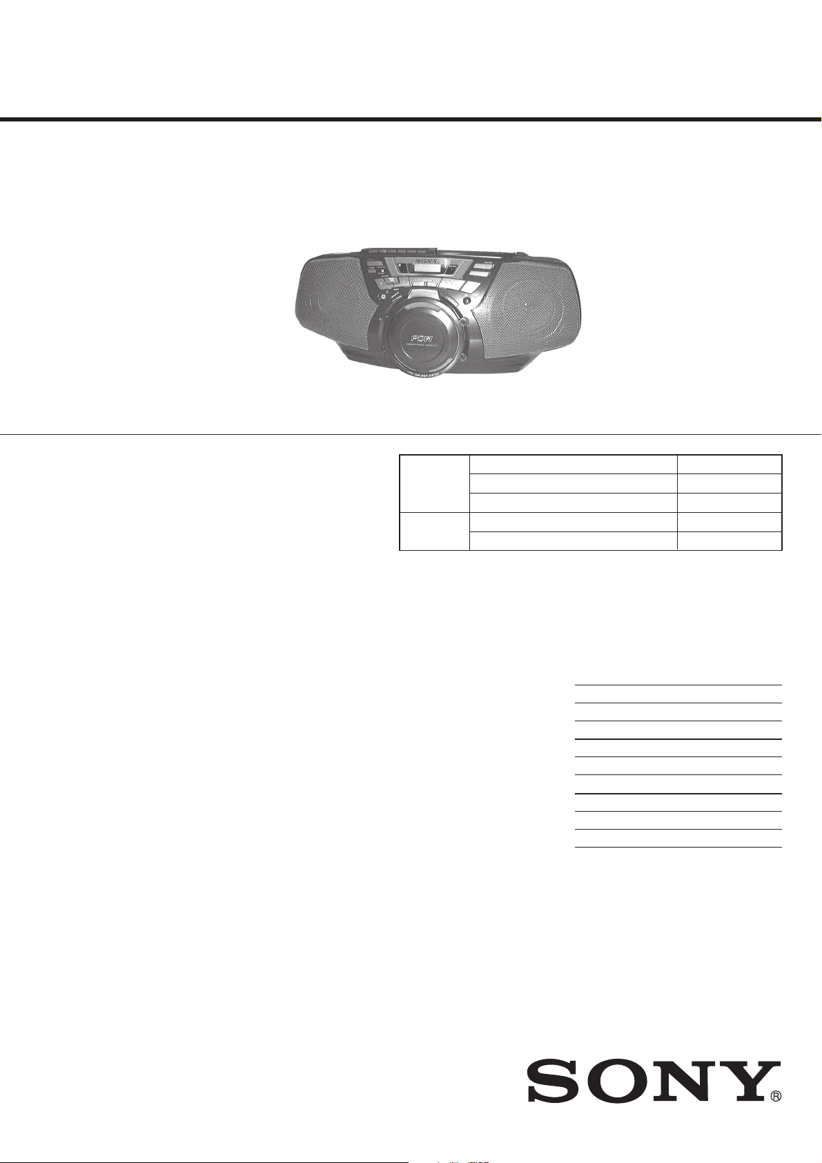
CFD-G30L/G50L
SERVICE MANUAL
Ver 1.1 2001.04
PHOTO : CFD-G50L
CD
Section
Tape deck Model Name Using Similar Mechanism CFD-V27L
Section T ape Transport Mechanism T ype MF-V5-117
AEP Model
UK Model
Singapore Model
CFD-G30L/G50L
Australian Model
CFD-G30L
Argentina Model
CFD-G50L
Model Name Using Similar Mechanism CFD-V27L
CD Mechanism Type KSM-213CDP
Optical Pick-up Name KSS-213C
SPECIFICATIONS
CD player section
System Compact disc digital audio system
Laser diode properties Material: GaAlAs
Wavelength:780 nm
Emission duration : Continuous
Laser output : Less than 44.6 µW
(This output is the value measured at a distance of
about 200 mm from the objective lens surface on
the optical pick-up block with 7 mm aperture.)
Spindle speed 200 r/min (rpm) to 500 r/min (rpm) (CLV)
Number of channels 2
Frequency response 20 – 20,000 Hz + 0.5/-1.5 dB
Wow and flutter Below measurable limit
Radio section
Frequency range FM : 87.5 – 108 MHz
MW : 531 – 1,602 kHz
LW : 153 – 279 kHz
IF FM : 10.7 MHz
MW/LW : 450 kHz
Aerials FM : Telescopic aerial
MW/LW : Built-in ferrite bar aerial
Cassette-corder section
Recording system 4 -track 2 channel stereo
Fast winding time Approx. 110 sec. with Sony cassette C-60
Frequency response TYPE I (normal) : 70 – 13,000 Hz
General
Speaker Full range : 10 cm (4 in.) dia., 3.2 Ω, cone type (2)
W oofer : 8 cm (3 1/4 in.) dia., 4 Ω, cone type (1)
Inputs LINE IN (stereo minijack) : Sensetivity 436 mV
Outputs Headphones jack (stereo minijack)
For 16 – 68 Ω impedance headphones
Maximum power output Full range : 4 W + 4 W
Woofer : 12W
Power requirements For CD radio cassette-corder :
230V AC, 50 Hz
12V DC, 8 size D (R 20) batteries
For remote contorol (CFD-G50L only):
3V DC, 2 size AA (R6) batteries
Power consumption AC 30W
Battery life For CD radio cassette-corder:
FM recording
Sony R20P : approx. 8 h
Sony alkaline LR20 : approx. 18 h
Tape playback
Sony R20P : approx. 1.5 h
Sony alkaline LR20 : approx. 6 h
CD playback
Sony R20P : approx. 1 h
Sony alkaline LR20 : approx. 4 h
Dimensions Approx. 500 × 206 × 328 mm (w/h/d)
(19 3/4 × 8 1/8 × 13 inches) (incl. projecting
parts)
Mass Approx. 7 kg (15 lb. 7 oz) (incl. batteries)
Supplied accessories Mains lead (1)
Remote control (1) (CFD-G50L only)
Design and specifications are subject to change without notice.
CD RADIO CASSETTE-CORDER
9-927-696-12
2001D1600-1
© 2001.4
Sony Corporation
Personal Audio Company
Shinagawa Tec Service Manual Production Group

TABLE OF CONTENTS
1. SERVICE NOTES ···························································· 3
2. GENERAL ·········································································· 4
3. DISASSEMBLY
3-1. Front Cabinet Assy ····························································· 5
3-2. Control-1, Headphone Board ············································· 6
3-3. Cabinet (Upper) Assy ························································· 6
3-4. Power, Batt, Tuner, Batt Com Board ·································· 7
3-5. Main, Line In, LCD Board ················································· 7
3-6. CD Board, Optical Pick-up Section,
Mechanism Deck ································································ 8
3-7. Belt ····················································································· 8
4. ADJUSTMENT
4-1. Mechanical Adjustment ······················································ 9
4-2. Electrical Adjustment ························································· 9
5. DIAGRAM
5-1. Circuit Boards Location ··················································· 12
5-2. Block Diagrams – Tuner/CD Section –···························· 13
– Main Section –······························································· 15
5-3. Schematic Diagram – CD Section –································· 18
5-4. Printed Wiring Board – CD Section – ······························ 21
5-5. Schematic Diagram – Cassette Deck Section –················ 23
5-6. Printed Wiring Board – Cassette Deck Section –············· 25
5-7. Schematic Diagram – Tuner Section – ····························· 27
5-8. Printed Wiring Board – Tuner Section – ·························· 29
5-9. Printed Wiring Board – Main Section – ··························· 31
5-10. Schematic Diagram – Main Section (1/2) – ····················· 33
5-11. Schematic Diagram – Main Section (2/2) –····················· 35
5-12. Printed Wiring Board and Schematic Diagram
– Control Section –·························································· 37
5-13. Schematic Diagram – Power Section – ···························· 39
5-14. Printed Wiring Board – Power Section – ························· 41
5-15. IC Pin Function Description············································· 43
5-16. IC Block Diagrams ··························································· 45
6. EXPLODED VIEWS
6-1. Front Cabinet Section ······················································· 49
6-2. Rear Cabinet Section ························································ 50
6-3. Upper Cabinet Section······················································ 51
6-4. Mechanism Deck Section (1) (MF-V5-117) ···················· 52
6-5. Mechanism Deck Section (2) (MF-V5-117) ···················· 53
6-6. Optical Pick-up Section (KSM-213CDP) ························ 54
7. ELECTRICAL PARTS LIST ··································· 55
SAFETY CHECK-OUT
After correcting the original service problem, perform the following
safety checks before releasing the set to the customer.
1. Check the area of your repair for unsoldered or poorly-soldered
connections. Check the entire board surface for solder splashes
and bridges.
2. Check the interboard wiring to ensure that no wires are
"pinched" or contact high-wattage resistors.
3. Look for unauthorized replacement parts, particularly
transistors, that were installed during a previous repair . Point
them out to the customer and recommend their replacement.
SAFETY-RELATED COMPONENT WARNING!!
COMPONENTS IDENTIFIED BY MARK 0 OR DOTTED LINE WITH
MARK 0 ON THE SCHEMATIC DIAGRAMS AND IN THE PARTS
LIST ARE CRITICAL TO SAFE OPERATION. REPLACE THESE
COMPONENTS WITH SONY PARTS WHOSE PART NUMBERS
APPEAR AS SHOWN IN THIS MANUAL OR IN SUPPLEMENTS
PUBLISHED BY SONY.
4. Look for parts which, through functioning, show obvious signs
of deterioration. Point them out to the customer and
recommend their replacement.
5. Check the B+ voltage to see it is at the values specified.
6. Flexible Circuit Board Repairing
• Keep the temperature of the soldering iron around 270˚C
during repairing.
• Do not touch the soldering iron on the same conductor of the
circuit board (within 3 times).
• Be careful not to apply force on the conductor when soldering
or unsoldering.
— 2 —
SECTION 1
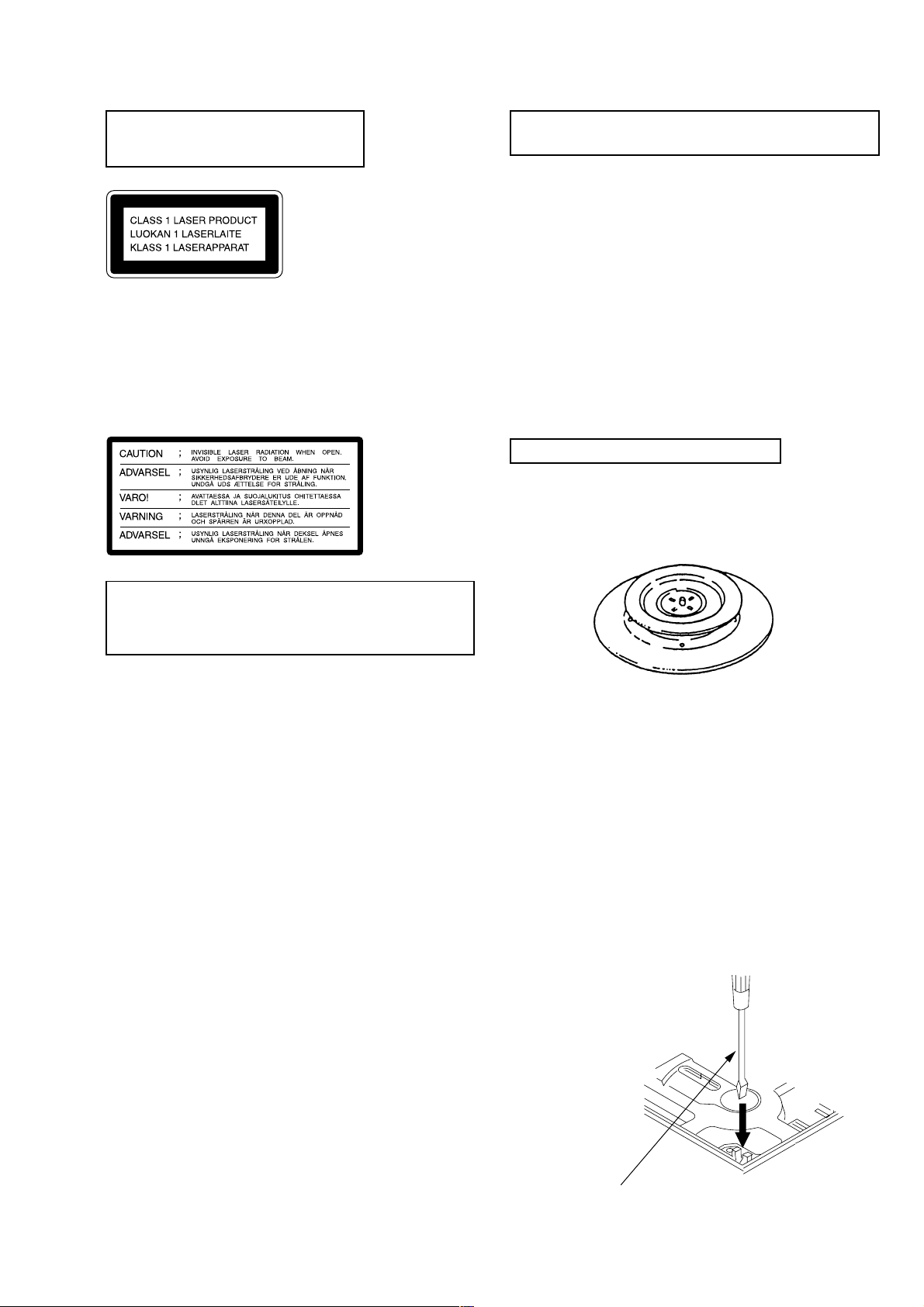
Insert a precision screw driver
and push SWITCH (S701)
SERVICE NOTES
Laser component in this product is capable
of emitting radiation exceeding the limit for
Class 1.
This appliance is classified as a CLASS 1 LASER product. The
CLASS 1 LASER PRODUCT MARKING is located on the rear
exterior.
The following caution label is located inside the unit.
NOTES ON HANDLING THE OPTICAL PICK-UP
BLOCK OR BASE UNIT
The laser diode in the optical pick-up block may suffer electrostatic
breakdown because of the potential difference generated by the
charged electrostatic load, etc., on clothing and the human body.
During repair, pay attention to electrostatic breakdown and also use
the procedure in the printed matter which is included in the repair
parts.
The flexible board is easily damaged and should be handled with
care.
NOTES ON LASER DIODE EMISSION CHECK
The laser beam on this model is concentrated so as to be focused on
the disc reflective surface by the objective lens in the optical pickup block. Therefore, when checking the laser diode emission,
observe from more than 30 cm away from the objective lens.
CHUCK PLATE JIG ON REPAIRING
On repairing CD section, playing a disc without the CD lid, use
Chuck Plate Jig.
• Code number of Chuck Plate Jig : X-4918-255-1
CAUTION
Use of controls or adjustments or performance of procedures
other than those specified herein may result in hazardous radiation
exposure.
LASER DIODE AND FOCUS SEARCH OPERATION
CHECK
1. Press CD open knob.
2. Open the lid for CD.
3. Push on SWITCH (S701) as following figure.
4. Confirm the laser diode emission while observing the objecting
lens. When there is no emission, Auto Po wer Control circuit or
Optical Pick-up is broken.
Objective lens moves up and down once for the focus search.
— 3 —
LOCATION AND FUNCTION OF CONTROLS
SECTION 2
GENERAL
,wf,wg,wh
wd
qlqkqj w;
qh
qg
qf
qd
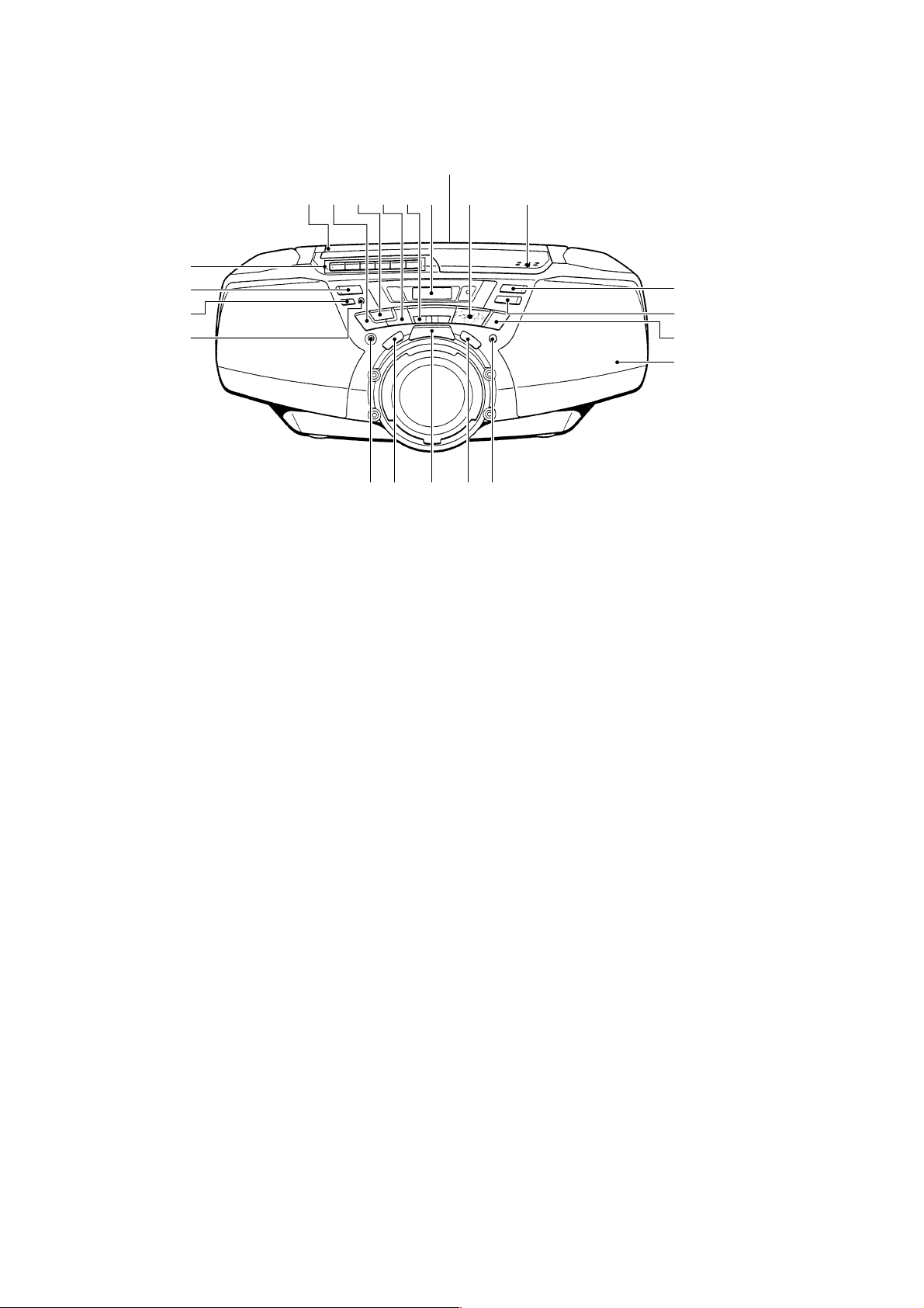
1 CD Z PUSH OPEN/CLOSE button
2 CD LID
3 CD u button
4 VOLUME + button
5 VOLUME − button
6 CD x button
7 Speaker
8 LINE button
9 SOUND button
0 POWER DRIVE WOOFER button
qa PLAY MODE (MONO/ST) button
qs i Phone jack
qd DISPLAY ENT MEMORY button
qf SLEEP button
qg POWER button
wa
3ws
1,2
8qs 0 9qa
qh Tape operation buttons
z button
N button
m button
M button
x, Z button
X button
qj CASSETTE LID
qk PRESET − button
ql RADIO BAND AUTO PRESET button
w; PRESET + button
wa TUNE ., > buttons
ws Information display OPR/BATT indicator
wd AC IN jack
wf FM rod antenna
wg Battery compartment
wh LINE IN jack
4
5
6
7
— 4 —
SECTION 3
DISASSEMBLY
• The equipment can be removed using the following procedure.
Cabinet (front) sub assySet
Cabinet (upper) assy
Control-1, Headphone board
Note : Follow the disassembly procedure in the numerical order given.
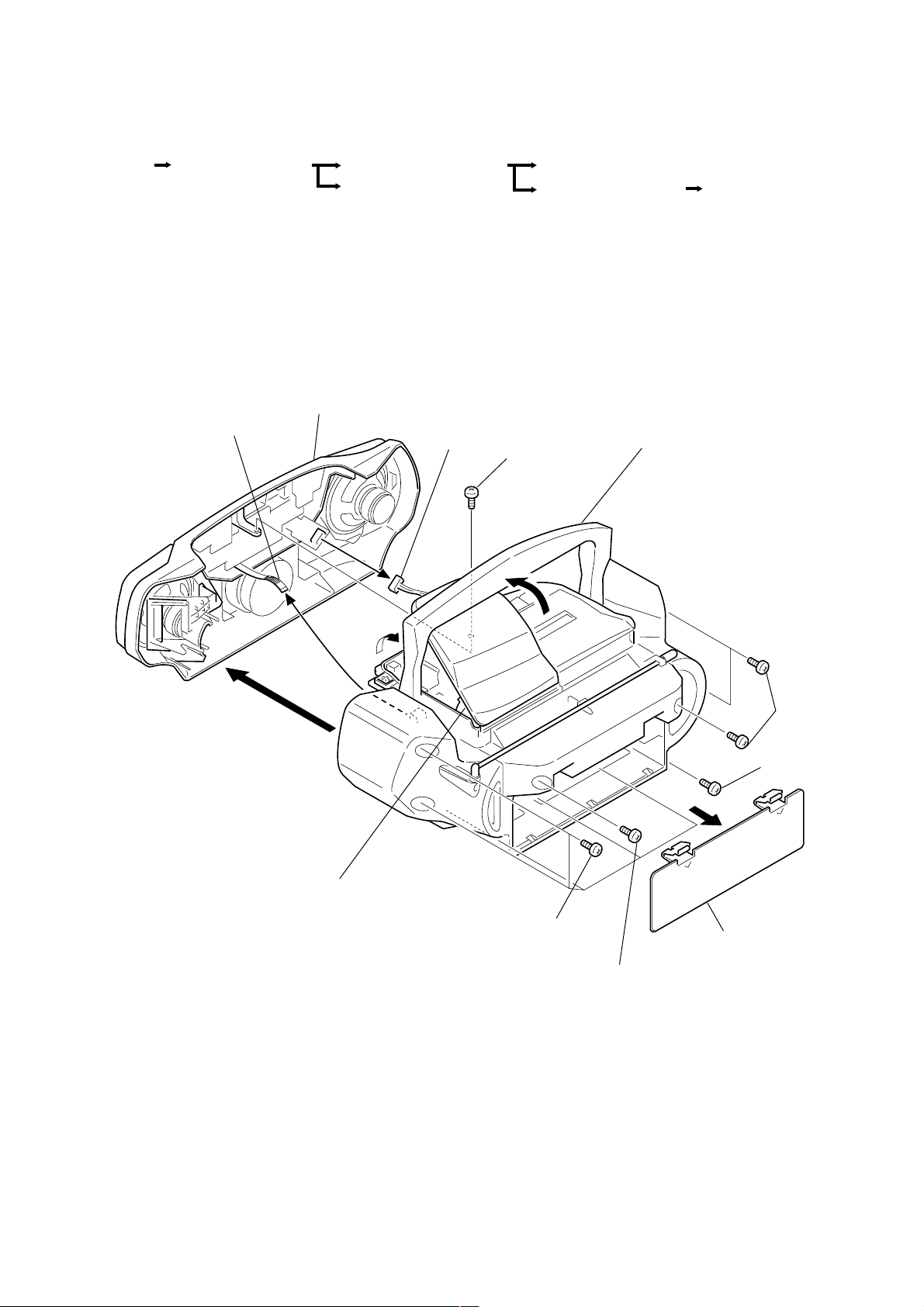
3-1. FRONT CABINET ASSY
qa Cabinet (front) sub assy
9 Flexible
0 Connector
8 Screw
+BVTP 3 × 10
Power, Batt, Tuner, batt com board
Main, LIine in, Lcd board CD board,
Optical pick-up section,
Mechanism deck, belt
6 Remove the Handle
in the direction of the arrow.
7 Open the Lid (CD) in
the direction of the arrow.
2 Five screws
+BVTP 3 × 12
4 Screw
+BVTP 3 × 16
3 Three screws
+BVTP 3 × 12
5 Screw
+BVTP 3 × 16
1 Lid, battery case
— 5 —
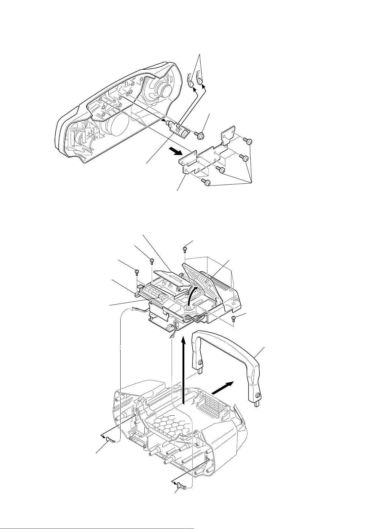
3-2. CONTROL-1, HEADPHONE BOARD
8
4 HEADPHONE board
3-3. CABINET (UPPER) ASSY
2 Open the cassette the holder assy by
pressing STOP/EJECT button.
3 Screw
+BVTP 3 × 10 BZN
6 T wo screws
+BVTP 3 × 10 CZN
5 T wo connectors
2 CONTROL-1 board
1 Four screws
+BVTP 3 × 10 BZN
3 Screw
+PWH 2.6 × 10
1 T en screws
+BVTP 2.6 ×
4 Open the CD lid in
the direction of the arrow.
0 Cabinet (upper) assy
STOP/EJECT
button
7 Connector
5 Screw
+BVTP 3 × 10 BZN
qa Open the Handle in
the direction of the arrow.
9
8 Connector
— 6 —
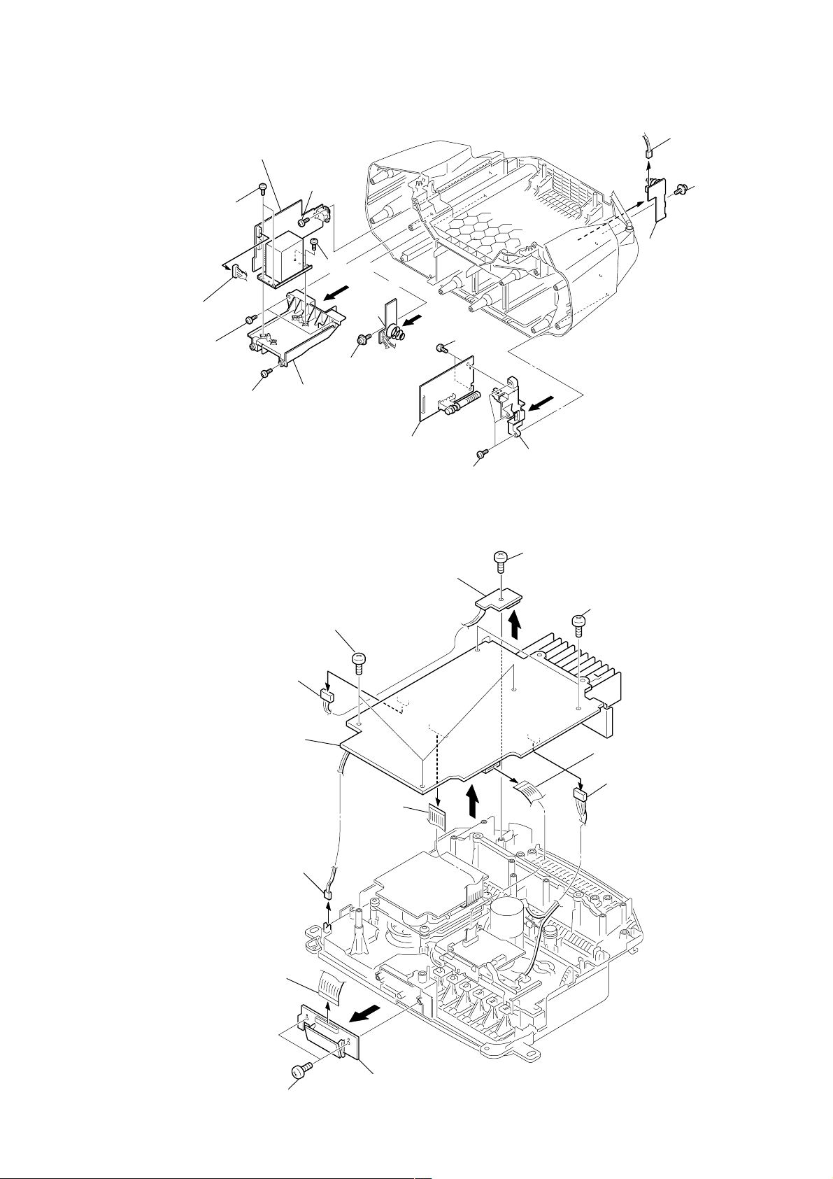
3-4. POWER, BATT, TUNER, BATT COM BOARD
8 Power board
1 Screw
+BVTP 3 × 12
6 T wo screws
+BVTP 3 × 16
5 T wo screws
+BVTP 3 × 10
7 Connector
2 T wo screws
+BVTP 3 × 12
3 T wo screws
+BVTP 3 × 12
0 BATT
board
9 Screw
+WH 3 × 8
4 Chassis (TRANS)
qh Connector
qg Screw
+WH 3 × 8
qj BATT COM board
qd T wo screws
+BVTP 3 × 10
3-5. MAIN, LINE IN, LCD BOARD
1 Three screws
+BVTP 3 × 12
6 Connector
0 Main board
qf TUNER board
5 Flexible
qs Chassis (TU)
qa Three screws
+BVTP 3 × 10
qa Screw
+BVTP 3 × 12
qs LINE IN board
2 T wo screws
+BVTP 3 × 12
4 Flexible
8 Connector
3
7 Connector
9 Flexible
qd T wo screws
+BVTP 3 × 10
qf LCD board
— 7 —
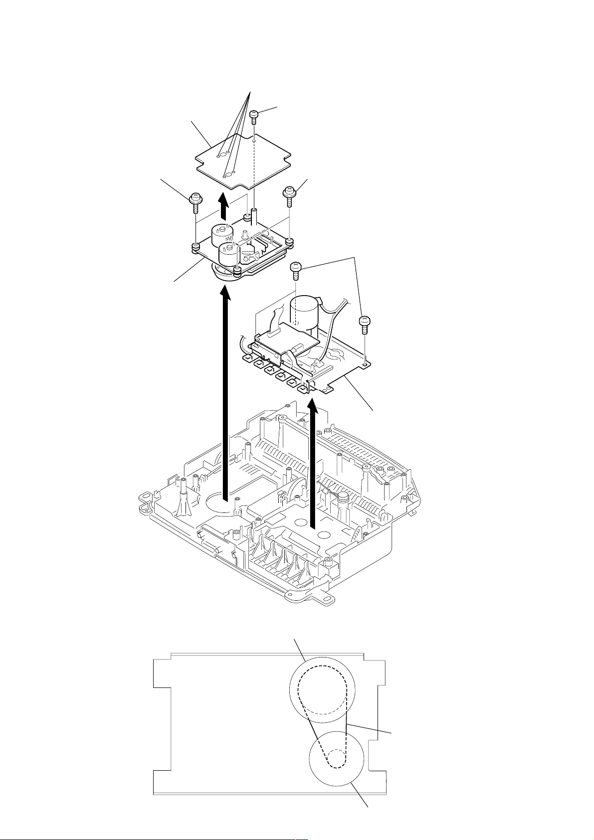
3-6. CD BOARD, OPTICAL PICK-UP SECTION, MECHANISM DECK
t
1 Remove solder
2 Screw
3 CD board
+P 2 × 6
4 T wo screws
+PWH 2.6 × 10
6 Optical pick-up section
5 T wo screws
+PWH 2.6 × 10
7 Three screws
+BVTP 3 × 10
8 Mechanism deck section
3-7. BELT
Flywheel assy
Bel
Motor assy
— 8 —
SECTION 4
ADJUSTMENTS
4-1. MECHANICAL ADJUSTMENT
PRECAUTION
1. Clean the following parts with a denatured-alchool-moistened
swab:
record/playback head pinch roller
erase head rubber belts
capstans
2. Demagnetize the record/playback head with a head
demagnetizer. (Do not bring the head demagnetizer close to
the erase head.)
Torque Measurement
Mode
FWD
FWD
back tension
Fast Forward
Rewind
T ape Tension Measurement
Torque Meter
CQ-403A
Torque Meter
CQ-102C
CQ-201B
Meter Reading
18 – 60 g•cm
(0.25 – 0.83 oz•inch)
1.0 – 5.0 g•cm
(0.014 – 0.069 oz•inch)
45 – 95 g•cm
(0.62 – 1.32 oz•inch)
45 – 95 g•cm
(0.62 – 1.32 oz•inch)
Meter Reading
more than 60 g
(more than 2.12 oz)
4-2. ELECTRICAL ADJUSTMENT
0dB = 0.775V
TAPE RECODER SECTION
Standard output level
Output
Load impedance
Output signal level
Test tape
Test T ape
WS-48A
Tape Speed Adjustment
Procedure :
Mode : Playback
test tape
WS-48A
(3kHz, 0dB)
Adjustment V alue : normal tape speed
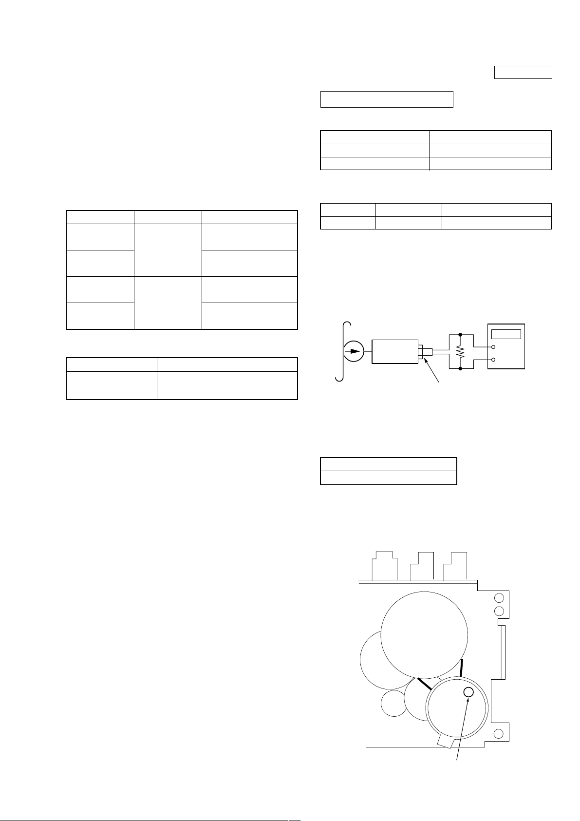
Adjust the tape speed adjustment control inside motor, so that the
frequency counter reading becomes 3,000 Hz.
Signal
3 kHz, 0 dB
set
Tape speed adjustment
J391 (phones)
HP OUT
32 Ω
0.25 V (–10 dB)
Used for
digital frequency
counter
32 Ω
+
–
Specification V alue :
Digital frequency counter
2,940 – 3,060Hz
Frequency difference between the beginning and the end of the
tape should be within 1.5% (45 Hz).
Adjustment Location :
— 9 —
Tape speed adjustment
control inside motor
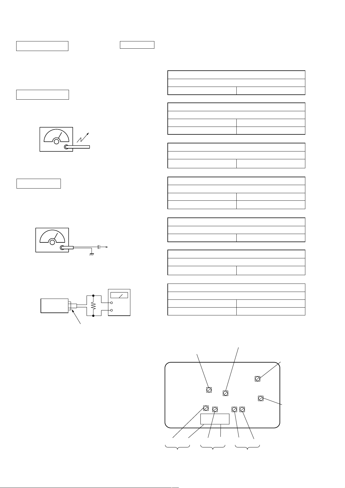
TUNER SECTION
c
r
• Switch Location
VOLUME : MAX
MEGA BASS : OFF
PRESET SOUND MODE : OFF
MW/LW SECTION
BAND : MW/LW
Signal generator
MW/LW RF signal
generator
30% amplitude modulation by 400Hz
signal.
Output level : as low as possible
0 dB = 1 µV
Put the lead-wire
antenna close to
the set.
• Repeat the procedures in each adjustment several times for the
maximum level meter indication.
• The frequency coverage and tracking adjustments should be
finally done by the trimmer capacitors.
AM IF ADJUSTMENT
Adjust for a maximum reading on level meter.
T2 450 kHz
MW TRACKING ADJUSTMENT
Adjust for a maximum reading on level meter.
L3-1 621 kHz
CT3 1,404 kHz
LW FREQUENCY COVERAGE ADJUSTMENT
Adjust for a maximum reading on level meter.
L4 279 kHz
FM SECTION
BAND : FM
Signal generator
FM RF signal
generator
75kHz (100%) amplitude modulation
by 1kHz signal.
Output level : as low as possible
set
0.01µF
32Ω
J391 (phones)
telescopi
antenna
terminal
level mete
+
–
L W TRACKING ADJUSTMENT
Adjust for a maximum reading on level meter.
L3-2 162 kHz
CT5 261 kHz
FM IF ADJUSTMENT
Adjust for a maximum reading on level meter.
T1 10.7 MHz
FM FREQUENCY COVERAGE ADJUSTMENT
Adjust for a maximum reading on level meter.
L2 108 MHz
FM TRACKING ADJUSTMENT
Adjust for a maximum reading on level meter.
L1 87.5 MHz
CT1 108 MHz
[Adjustment Location : Main board] (Component side)
L2
FM FREQUENCY COVER.
L4
LW FREQUENCY COVER.
Adjustment
Adjustment
T2
AM IF
Adjustment
T1
FM IF
Adjustment
CT5 L3-2
LW TRA CKING
Adjustment
CT3 L3-1
MW TRACKING
Adjustment
CT1 L1
FM TRACKING
Adjustment
— 10 —
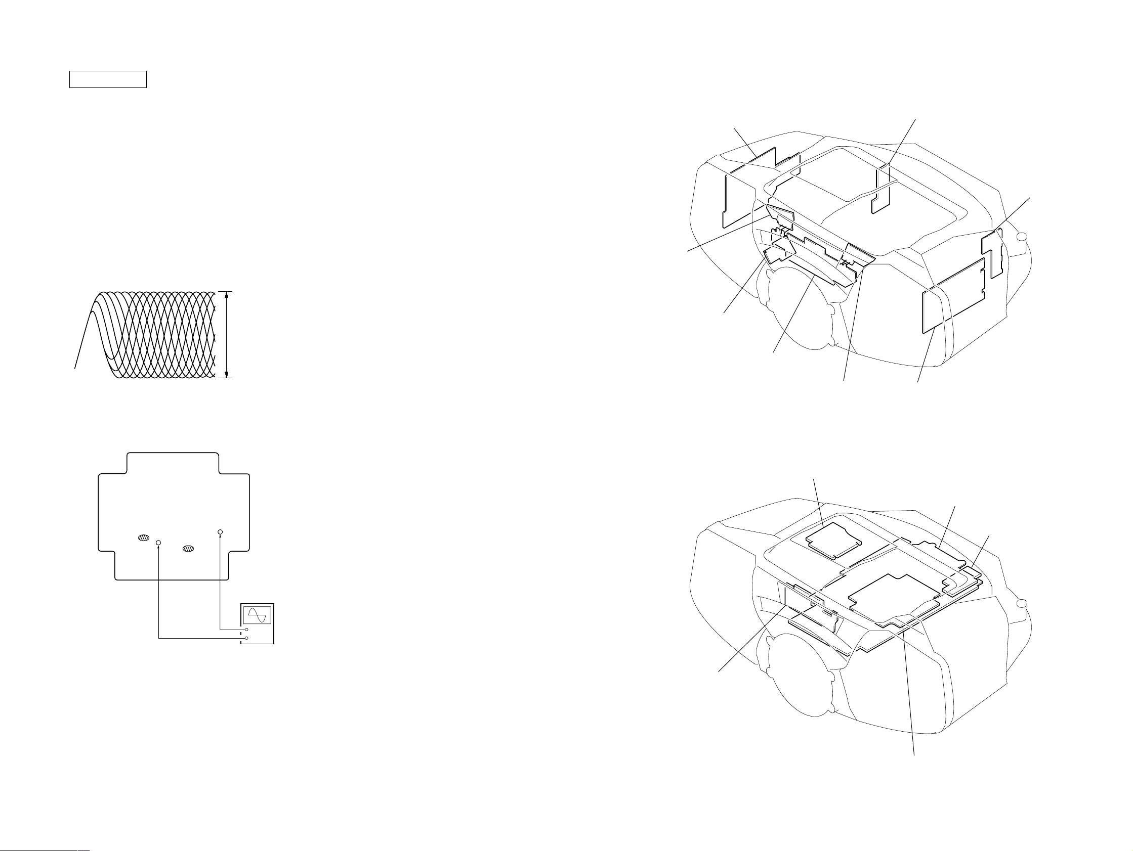
SECTION 5
s
DIAGRAMS
CD SECTION
Focus Bias Check
This check is to be done when the optical block replaced.
Check Procedure:
1. Connect the oscilloscope to test point TP (VC) and TP (RF) on
CD board.
2. Put the set into test mode.
3. Opitical pick-up setting to the center by + or – button pushing.
4. Insert disk (YEDS-18) and press u button.
5. Press the MODE button. (Tracking servo ON)
6. Check that the oscilloscope wavewform is as sho wn in the figure
below (eye pattern).
A good eye pattern means that the diamond shape (◊) in the
center of the waveform can be clearly distinguished.
7. Release test mode after adjustment is completed.
• RF signal reference waveform (eye pattern)
VOLT/DIV : 0.2V
TIME/DIV : 500n
0.9Vp-p – 1.3Vp-p
5-1. CIRCUIT BOARDS LOCATION
BATT board
POWER board
BATT COM board
CONTROL-2 board
HEADPHONE board
CONTROL-1 board
When observing the eye pattern, set the oscilloscope for AC range
and raise vertical sensivity.
[Adjustment Location : CD board] (Conductor side)
Oscilloscope
TP
(RF)
TP(VC)
(DC range)
+
–
LCD board
CONTROL-3 board
PRE board
TUNER board
MAIN board
LINE IN board
CD board
— 11 — — 12 —
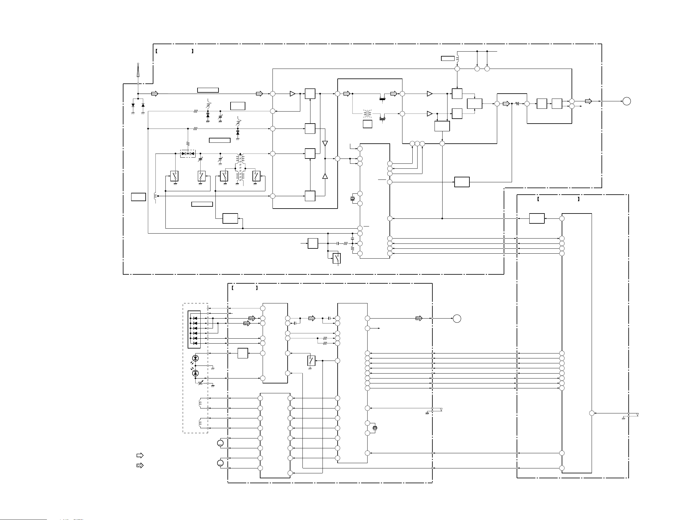
CFD-G30L/G50L
5-2. BLOCK DIA GRAMS – TUNER/CD SECTION –
ANT1
FM
TELESCOPIC
ANTENNA
LW
F-COVER.
TUNER BOARD
L4
RADIO 6V
Q44
LW
FM TRACKING
RADIO 6V
L1
D1
CT1
MW TRACKING
D3
CT5 -1
Q43
LW
L3-2,CT5
LW TRACKING
L3-1,CT3
CT3
Q41
MW
MW/LW
SWITCH
Q14
RADIO 6V
L2
D2
FM
F-COVER.
L3
FERRITE-ROD
ANTENNA
RADIO 6V
RADIO 6V
AM IF
IFOUT
10
QUAD
FM
DET
AM
DET
AM HCUT
Q12
T2
23 5
VCC1 VCC2
FM/AM
BUFFER
MPX
MPX
16
FM
15
MPX
MUTE
12
R-CH
11
L-CH
MAIN
A
SECTION
MAIN BOARD (1/2)
MASTER CONTROL
RADIO
MUTE
Q510
3
14
16
15
17
IC501(1/2)
MUTE
R COUNT
R DATA
R CLOCK
R LATCH
FRONT-END
IF AMP,DET,FM MPX
IC1
T1
FM
IF
VDD
FM
AM
XO
XI
MW/LW
LP OUT
LP IN
PD
CF2
CF4
PLL
IC2
MO/ST
13
ST IND
BAND
BAND
IF IN
10
DO
DI
CL
CE
FM IF
7
AM IF
6
IF
BUFFER
MO/ST
ST IND
BAND
14
18
13
8
7
9
4
2
3
1
18
MIX OUT
FM RF I
2
FM RF O
24
FM OSC
21
AM RF
22
Q42
MW
-2
AM OSC
20
FM
MIX
FM
OSC
AM
MIX
AM
OSC
VT
LPF
OSC
4
6V
14
19
VT
X1
75kHz
Q61
REG
12
11
20
19
6
18
17
16
• RCH is omitted
• Signal Path
: FM
: CD
OPTICAL PICK-UP
BLOCK
(KSS-213C)
VC
A
B
C
D
E
F
LD
GND
PD
VR
F+
FOCUS
COIL
F-
COIL
T+
T-
TRACKING
16
M701
SLED
MOTOR
M702
SPINDLE
MOTOR
M
M
CD BOARD
D VDD
Q701
LD
DRIVE
RF AMP
IC701
10
VC
4
PD1
5
PD2
8
E
7
F
2
LD ON
LD
AGC CONT
3
PD
MOTOR/COIL DRIVE
IC703
17
F+
18
F-
13
T+
14
T-
12
SL+
11
SL-
15
SP+
16
SP-
RFO
RFI
FFDR
FRDR
TFDR
TRDR
SRDR
SFDR
SP IN
MUTE
DIGITAL SERVO
DIGITAL SIGNAL PROC.
D/A CONV.
IC702
15
16
13FE
11TE
19
Q702
18
24
23
2
3
6
5
25
20
51
43
39
41
40
14
32
33
30
31
29
28
26
RFAC
RFDC
FE
TE
SE
XLON
FFDR
FRDR
TFDR
TRDR
SRDR
SFDR
MDP
L OUT
DATA
CLK
XLAT
SQCK
SCLK
SCOR
SQSO
SENS
SSTP
XRST
72
R-CH
75R OUT
5
7
6
2
9
20
1
8
27
66XTAI
X101
16.9344MHz
67XTAO
3
L OUT
S702
LIMIT
IN SW
MAIN
B
SECTION
12
C DATA
10
C CLOCK
11
C LATCH
7
C SQCK
5
C SCLK
1
C SCOR
8
C SQSO
6
C SENS
S701
(CD DOOR)
9
C XRST
13
C AGC CONT
C DOOR
80
— 13 — — 14 —
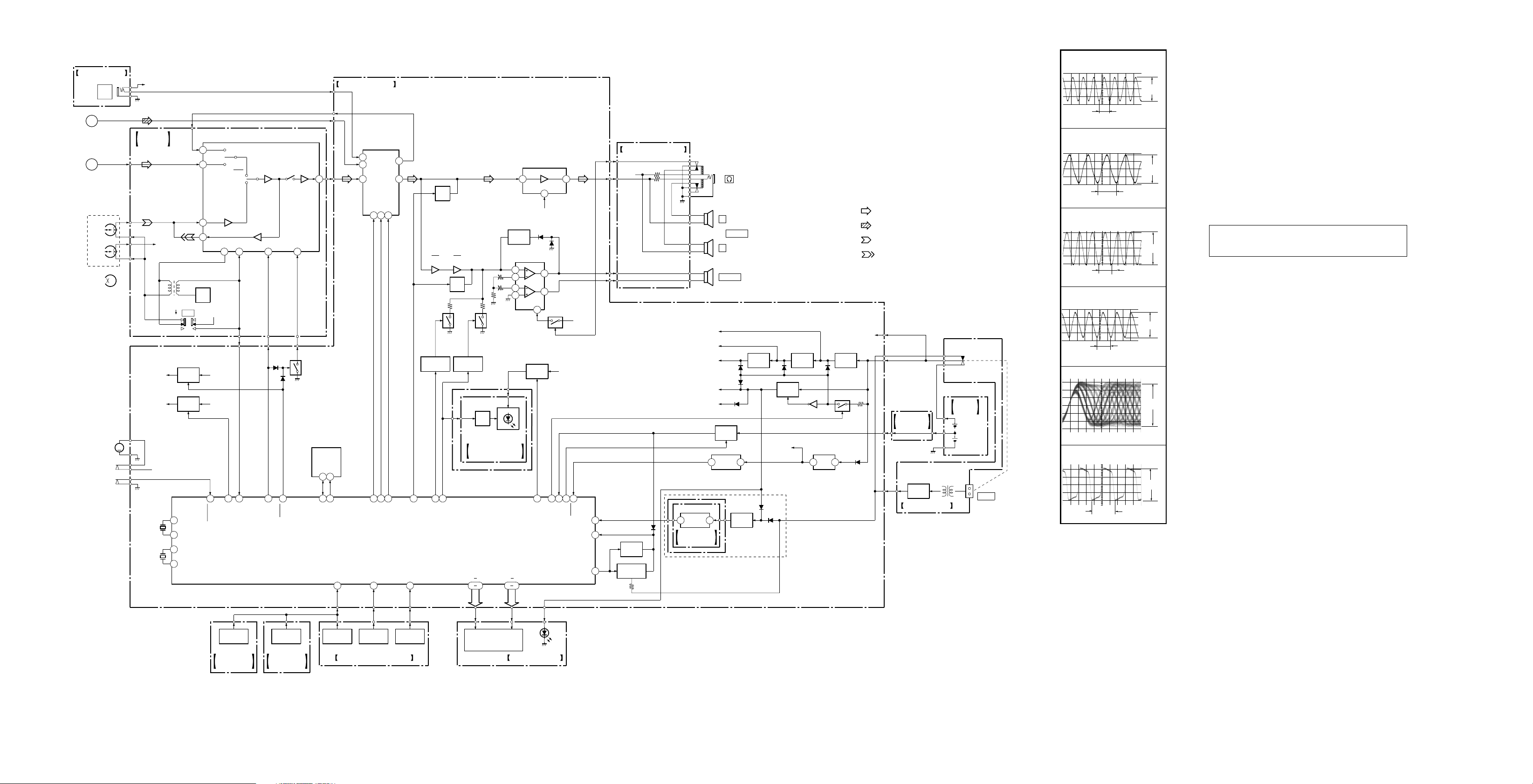
CFD-G30L/G50L
– MAIN SECTION –
LINE IN BOARD
J301
LINE
IN
HEAD
HEAD
L OUT
B
L-CH
A
L-CH
R-CH
M321
(LOADING)
S322
(MOTOR SW)
S321
(PLAY SW)
M
TUNER/CD
SECTION
TUNER/CD
SECTION
HRP301
REC/PB
HE301
ERASE
R-CH
PRE AMP
BOARD
R-CH
R-CH
RADIO 6V
D VDD
MOTOR SW B+
X502
153kHz
X501
4MHz
T301
REC
PB
73
74
32
31
S301
REC
SWITCH
Q513,514
SWITCH
Q511,512
TX
TEX
XTAL
EXTAL
Q301
BIAS
OSC
24
22
5
4
L IN
RADIO
AUDIO 6V
AUDIO 6V
COM3.3V
79
TC PLAY
TAPE
TAPE
PB AMP
REC TAPE
REF
6
71
CD
WAVEFORMS
1
IC2 w;
MAIN BOARD(2/2)
13.3us
PRE AMP
IC301
BUFFER
AMP
REC AMP
26dB
1521
D501
D502
REC
69
TAPE
23
70
RADIO
LINE
7dB
L
20
17
Q515
EEP ROM
IC504
65
24
SCL77SDA
25
KEY1
SOUND/VOLUME
IC321
13
S IN
14
S IN
9
IN
DATA
1
30CE2
20
19
V DATA
IC501(2/2)
SYSTEM CONTROL
KEY2
26
S OUT
L OUT
CLK
18
V LATCH
V CLOCK
HEADPHONE BOARD
12
BASS AGC
Q326,327
WOOFER
POWER AMP
12
13
10
11
COM3COM0
4138
POWER AMP
IC324
STBY
VCC
SWITCH
Q518,519
IC323
STBY
8
VDD(S.W)
3
5
8
28
LIGHT CONT
21
Q322
22
P CON
3
AUDIO 6V
65VM30
REG CHK
VDD(S.W)
RESET
INIT
VDD(S.W)
R VT
31
J391
SP391
L
SP392
R
SP393
WOOFER
BATTRY
CHECK
Q503,504
IC503
RESET
SPEAKER
D955
D955
D951
D322
RMC REG
Q509
• RCH is omitted
• Signal Path
: FM
: CD
: PB
: REC
POWER AMP B+
IC502
3.3V
REG
23
9V REG
Q954
Q951
D503
BATT COM
BOARD
RECT
D901-904
POWER BOARD
T901
BATT
BOARD
POWER
BATT
1.5x8=12V
J901
~AC IN
3.3V REG
Q956
µ COM(VDD)
21
D507
D508
6V REG
Q955
D952 D958
POWER
SWITCH
Q952
Q953
G50L
MODEL
R-CH
MOTOR SW B+
AUDIO +6V
COM +3.3V
IC651
2RMC
29MODE CHK
62
MODE
CHECK
Q507
AC/DC
DISTINCTION
Q505,506
D512
REMOTE
CONTROL
LCD BOARD
(2/2)
21
5
MUTE
Q122
L.P.F
IC322
2157
MUTE
Q321
Q328Q329
WOOFER
GAIN CONT
Q517
WOOFER
GAIN CONT
Q516
LED
DRIVE
Q601
D601
D603,604
CONTROL-1 (1/2)
BOARD
76
64
A MUTE
WOOFER 163WOOFER 2
KEY3
27
SEG17SEG0
4942
2
3
4
5
6
IC501 ea
IC501 uf
T301
IC702 ta
IC702 yj
250ns
6.5us
18.0us
59ns
1.5Vp-p
500mV/div
10µsec/div
3.6Vp-p
1V/div
100nsec/div
2.0Vp-p
500mV/div
5µsec/div
32.0Vp-p
1V/div
10µsec/div
1.1Vp-p
400ns/div
200mV/div
4.0Vp-p
1V/div
20nsec/div
Note on Printed Wiring Board:
• X : parts extracted from the component side.
• Y : parts extracted from the conductor side.
• b : Pattern from the side which enables seeing.
Note on Schematic Diagrams:
• All capacitors are in µF unless otherwise noted. pF: µµF
50 WV or less are not indicated except for electrolytics
and tantalums.
• All resistors are in Ω and 1/
specified.
f
•
: internal component.
4
W or less unless otherwise
• 2 : nonflammable resistor.
• C : panel designation.
• H : adjustment for repair.
• U : B+ Line.
• Power voltage is dc 12 V and fed with regulated dc po wer
supply from battery terminal.
• Voltages and wavefor ms are dc with respect to ground
under no-signal (detuned) conditions.
Note : The components identified by mark 0 or dotted
line with mark 0 are critical for safety.
Replace only with part number specified.
– For Radio, TAPE section MAIN (1/2) –
no mark : PLAY (TAPE SECTION)
TAPE STOP
( ) : REC (TAPE SECTION)
[ ] : FM (RADIO SECTION)
< > : AM (RADIO SECTION)
– For CD Section MAIN (2/2) –
no mark : CD PLAY
CD STOP
• Voltages are taken with a VOM (Input impedance 10 MΩ).
Voltage variations may be noted due to normal production tolerances.
• Signal path.
F : FM
f : MW/LW
E : PB
a : REC
J : CD
16
FUNCTION
SWITCH
S631,632
CONTROL-3
BOARD
FUNCTION
SWITCH
S621-623
CONTROL-2
BOARD
FUNCTION
SWITCH
FUNCTION
SWITCH
S603-607
CONTROL-1 BOARD(2/2)
FUNCTION
SWITCH
S608-611S601,602
LCD651
LIQUID CRYSTAL
DISPLAY PANEL
D651
(OPR/BATT)
LCD BOARD(1/2)
— 15 — — 16 — — 17 —
CFD-G30L/G50L
○○○○○○○○○○○○○○○○○○○○○○○○○○○○○○○○○○○○○○○○○○○○○○○○○○○○○○○○○○○○○○○○○○○○○○○○○○○○○○○○○○○○○○○○○○○○○○○○○○○○○○○○○○
○○○○○○○○○○○○○○○○○○○○○○○○○○○○○○○○○○○○○○○○○○○○○○○○○○○○○○○○○○○○○○○○○○○○○○○○○○○○○○○○○○○○○○○○○○○○○○○○○○○○○○○○○○
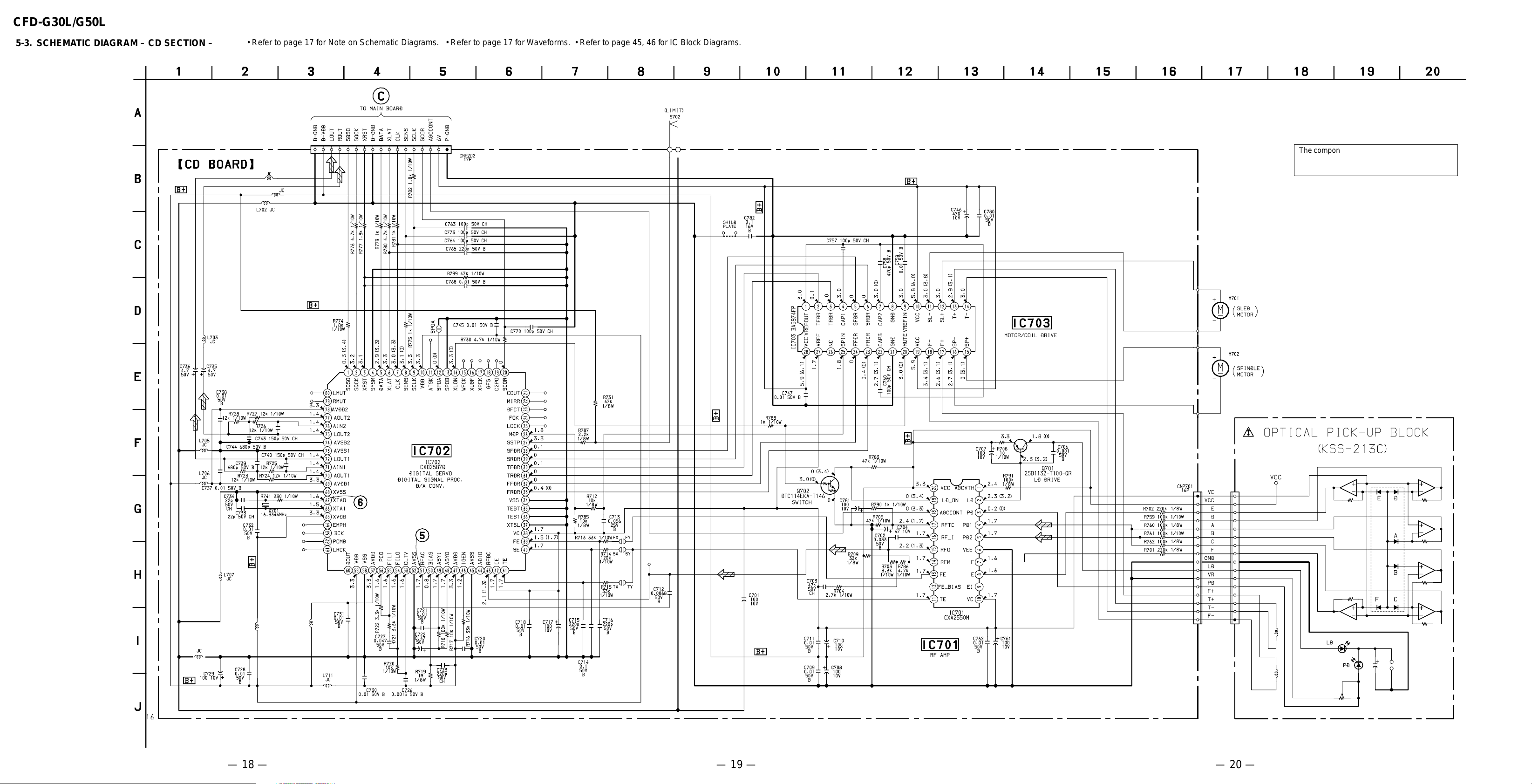
5-3. SCHEMATIC DIAGRAM – CD SECTION –
• Refer to page 17 for Note on Schematic Diagrams. • Refer to page 17 for Waveforms. • Refer to page 45, 46 for IC Block Diagrams.
(Page 35)
L704
L701
The components identified by mark 0 or dotted
line with mark 0 are critical for safety.
Replace only with part number specified.
L709
TP
(RF)
L708
JC
L710
JC
— 18 — — 19 — — 20 —
 Loading...