

Page 1
CFD-E100/E100L
CD player section
System
Compact disc digital audio system
Laser diode properties
Emission duration: Continuous
Laser output: Less than 44.6 µW
(This output is the value measured at a distance
of about 200 mm from the objective lens surface
on the optical pick-up block with 7 mm
aperture.)
Spindle speed
200 r/min (rpm) to 500 r/min (rpm)
(CLV)
Number of channels
2
Frequency response
20 - 20 000 Hz +1/–2 dB
Wow and flutter
Below measurable limit
Radio section
Frequency range
CFD-E100L
FM 87.5 - 108 MHz
MW 531 - 1 611 kHz (9 kHz step)
530 - 1 610 kHz (10 kHz step)
LW 153 - 279 kHz
CFD-E100
FM 87.5 - 108 MHz
AM 531 - 1 611 kHz (9 kHz step)
530 - 1 610 kHz (10 kHz step)
IF
FM: 10.7 MHz
AM/MW/LW: 450 kHz
Aerials
FM: Telescopic aerials
AM/MW/LW: Built-in ferrite bar aerials
Cassette-corder section
Recording system
4-track 2 channel stereo
Fast winding time
Approx. 120 s (sec.) with Sony cassette C-60
Frequency response
TYPE I (normal): 80 - 13 000 Hz
General
Speaker
Full range: 8 cm dia., 3.2 Ω, cone type (2)
Outputs
Headphones jack (stereo minijack)
For 16 - 68 Ω impedance headphones
Maximum Power output
3.6 W
Power requirements
For CD radio cassette-corder:
Korean
US, Canadian, Taiwan models:
120 V AC, 60Hz
model: 220 V AC, 60Hz
Other models: 230 V AC, 50Hz
9 V DC, 6 R14 (size C) batteries
For remote control:
3 V DC, 2 R03 (size AAA) batteries
Power consumption
AC 14 W
Battery life
For CD radio cassette-corder:
FM recording
Sony R14P: approx. 13.5 h
Sony alkaline LR14: approx. 20 h
Tape playback
Sony R14P: approx. 7.5 h
Sony alkaline LR14: approx. 15 h
CD playback
Sony R14P: approx. 2.5 h
Sony alkaline LR14: approx. 7 h
Dimensions
Approx. 385 × 190.5 × 170 mm (w/h/d)
(incl. projecting parts)
Mass
Approx. 3.1 kg (incl. batteries)
Supplied accessory
Mains lead (1)
Remote control (1)
Design and specifications are subject to change
without notice.
(US model only)
AUDIO POWER SPECIFICATIONS
POWER OUTPUT AND TOTAL
HARMONIC DISTORTION
With 3.2-ohm loads, both channels driven
from 100 - 10,000 Hz; rated 1.5 W per
channel-minimum RMS power, with no
more than 10 % total harmonic distortion
in AC operation.
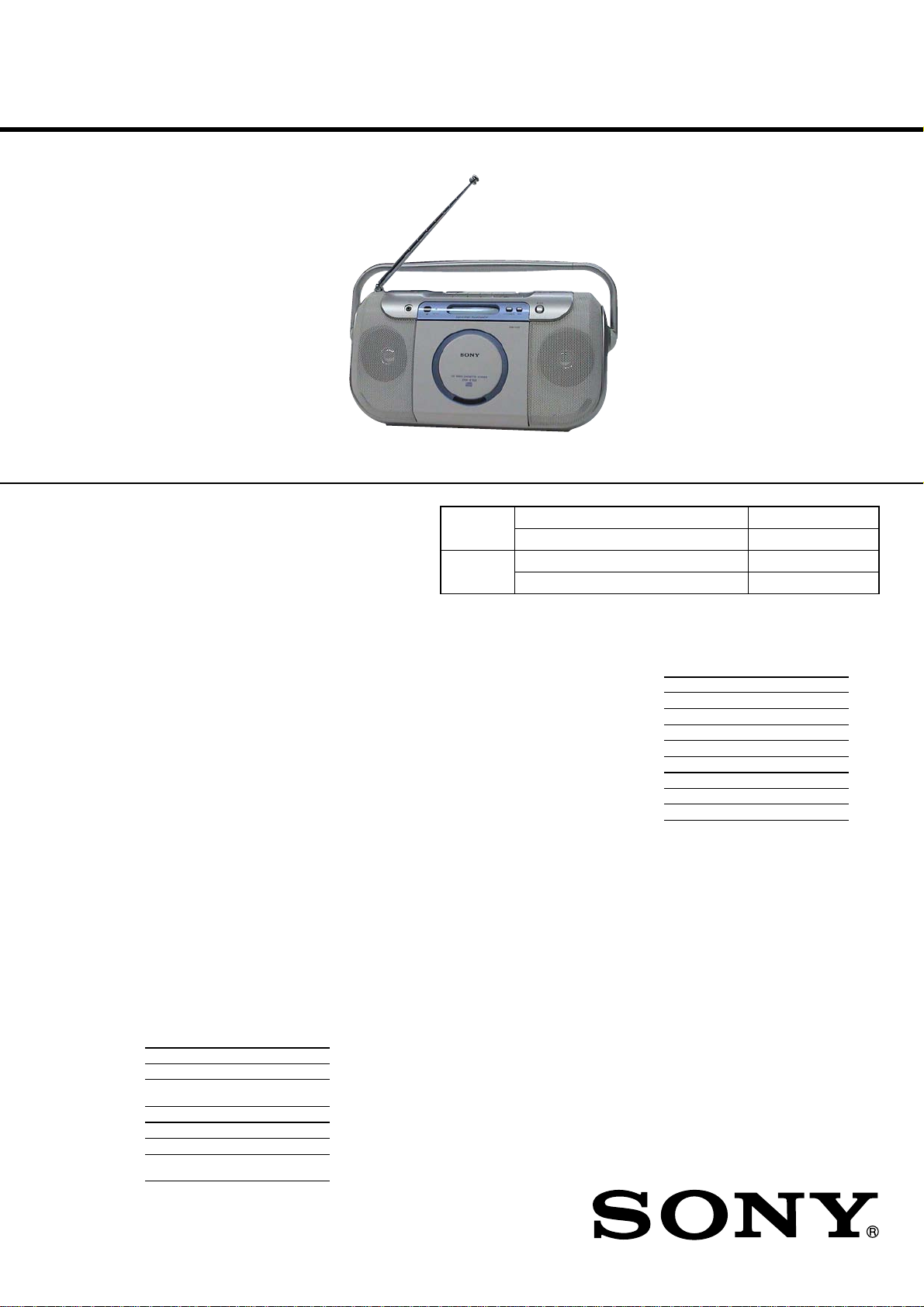
SERVICE MANUAL
Ver. 1.1 2005.05
Photo : CFD-E100
CD
Section
TAPE
Section
SPECIFICATIONS
US Model
Canadian Model
E Model
CFD-E100
AEP Model
UK Model
CFD-E100L
Model Name Using Similar Mechanism NEW
Optical Pick-up Block Name KSM-900AAA
Model Name Using Similar Mechanism NEW
Tape T ransport Mechanism T ype MF-E100
9-879-702-02
2005E05-1
© 2005.05
Sony Corporation
Personal Audio Group
Published by Sony Engineering Corporation
CD RADIO CASSETTE-CORDER
Page 2
CFD-E100/E100L
r
CAUTION
Use of controls or adjustments or performance of procedures
other than those specified herein may result in hazardous radiation
exposure.
Notes on chip component replacement
• Never reuse a disconnected chip component.
• Notice that the minus side of a tantalum capacitor may be
damaged by heat.
Flexible Circuit Board Repairing
• Keep the temperature of the soldering iron around 270 ˚C
during repairing.
• Do not touch the soldering iron on the same conductor of the
circuit board (within 3 times).
• Be careful not to apply force on the conductor when soldering
or unsoldering.
About CD-Rs/CD-RWs
This player can play CD-Rs/CD-RWs
recorded in the CD-DA format*, but
playback capability may vary depending on
the quality of the disc and the condition of
the recording device.
* CD-DA is the abbreviation for Compact
Disc Digital Audio. It is a recording
standard used for Audio CDs.
SAFETY CHECK-OUT
After correcting the original service problem, perform the following
safety check before releasing the set to the customer:
Check the antenna terminals, metal trim, “metallized” knobs, screws,
and all other exposed metal parts for AC leakage.
Check leakage as described below.
SAFETY-RELATED COMPONENT WARNING!!
COMPONENTS IDENTIFIED BY MARK 0 OR DOTTED LINE
WITH MARK 0 ON THE SCHEMATIC DIAGRAMS AND IN
THE PARTS LIST ARE CRITICAL TO SAFE OPERATION.
REPLACE THESE COMPONENTS WITH SONY PARTS WHOSE
PART NUMBERS APPEAR AS SHOWN IN THIS MANUAL OR
IN SUPPLEMENTS PUBLISHED BY SONY.
ATTENTION AU COMPOSANT AYANT RAPPORT
À LA SÉCURITÉ!
LES COMPOSANTS IDENTIFIÉS P AR UNE MARQ UE 0 SUR
LES DIAGRAMMES SCHÉMATIQUES ET LA LISTE DES
PIÈCES SONT CRITIQUES POUR LA SÉCURITÉ DE
FONCTIONNEMENT. NE REMPLACER CES COM- POSANTS
QUE PAR DES PIÈCES SONY DONT LES NUMÉROS SONT
DONNÉS DANS CE MANUEL OU D ANS LES SUPPLÉMENTS
PUBLIÉS PAR SONY.
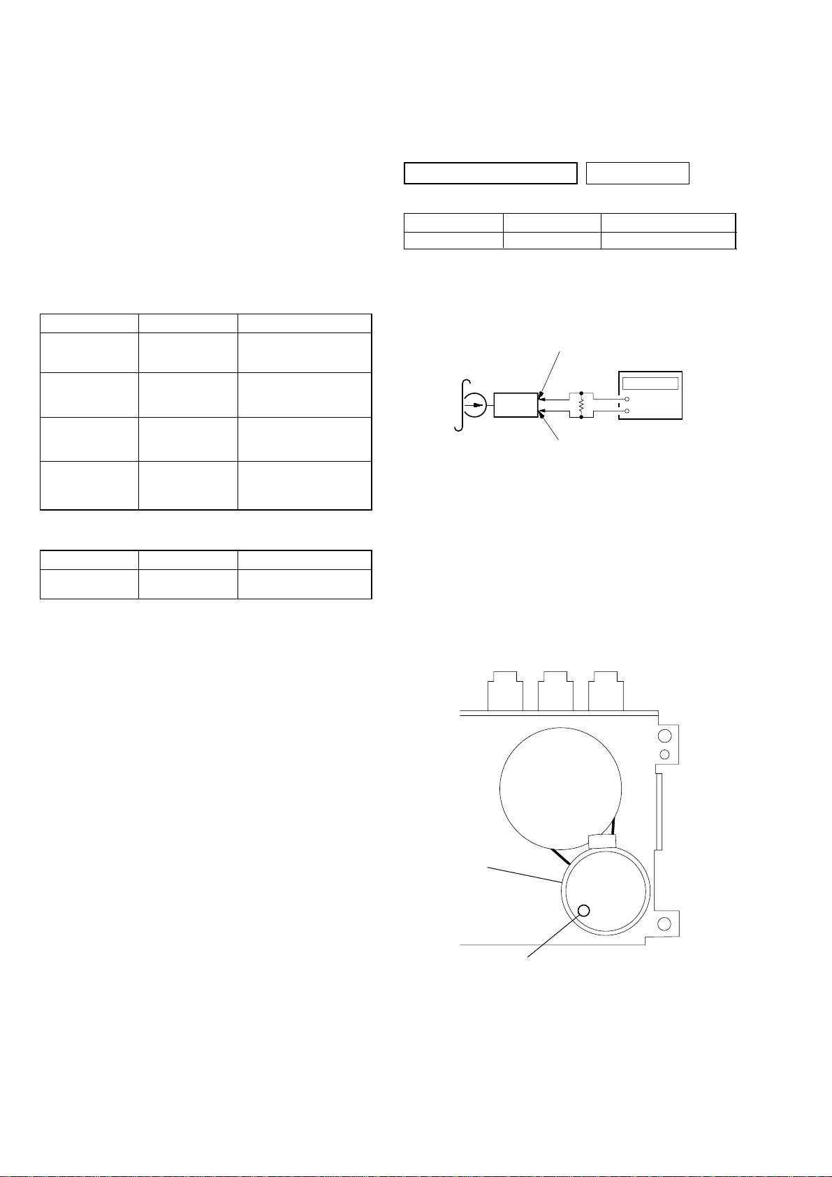
LEAKAGE TEST
The AC leakage from any exposed metal part to earth ground and
from all exposed metal parts to any exposed metal part having a
return to chassis, must not exceed 0.5 mA (500 microamperes.).
Leakage current can be measured by any one of three methods.
1. A commercial leakage tester, such as the Simpson 229 or RCA
WT-540A. Follow the manufacturers’ instructions to use these
instruments.
2. A battery-operated AC milliammeter. The Data Precision 245
digital multimeter is suitable for this job.
3. Measuring the voltage drop across a resistor by means of a
VOM or battery-operated AC voltmeter. The “limit” indication
is 0.75 V, so analog meters must have an accurate low-voltage
scale. The Simpson 250 and Sanwa SH-63Trd are examples
of a passive VOM that is suitable. Nearly all battery operated
digital multimeters that have a 2 V AC range are suitable. (See
Fig. A)
To Exposed Metal
Parts on Set
AC
0.15 µF
1.5 k
Ω
voltmete
(0.75 V)
Earth Ground
Fig. A. Using an AC voltmeter to check AC leakage.
2
Page 3

TABLE OF CONTENTS
1. SERVICING NOTES ................................................ 4
2. GENERAL ................................................................... 6
3. DISASSEMBLY
3-1. Disassembly Flow ........................................................... 7
3-2. Cover (Handle) ................................................................ 8
3-3. Handle Block ................................................................... 8
3-4. Cabinet (Rear) Block....................................................... 9
3-5. CD Tray Block ................................................................. 10
3-6. Optical Pick-up Block ..................................................... 10
3-7. Optical Pick-up (KSM-900AAA) ................................... 11
3-8. Panel (Upper) Block ........................................................ 11
3-9. MD Block ........................................................................ 12
3-10. MAIN Board .................................................................... 12
3-11. POWER Board ................................................................ 13
3-12. Tape Mechanism Deck (MF-E100) ................................. 13
3-13. RP Head (HRP301) ......................................................... 14
3-14. Motor Sub Assy (CAPSTAN/REEL) (M901) ................. 14
3-15. TU Board ......................................................................... 15
CFD-E100/E100L
4. MECHANICAL ADJUSTMENTS......................... 16
5. ELECTRICAL ADJUSTMENTS .......................... 16
6. DIAGRAMS
6-1. Block Diagram – SERVO Section – ............................... 21
6-2. Block Diagram – TUNER Section – .............................. 22
6-3. Block Diagram – AUDIO Section – ............................... 23
6-4. Block Diagram – PANEL, POWER SUPPLY Section – 24
6-5. Printed Wiring Boards – CD Section – .......................... 26
6-6. Schematic Diagram – CD Section –............................... 27
6-7. Printed Wiring Board
– TUNER Section (CFD-E100 Only) – .......................... 28
6-8. Schematic Diagram
– TUNER Section (CFD-E100 Only) – .......................... 29
6-9. Printed Wiring Board
– TUNER Section (CFD-E100L Only) – ........................ 30
6-10. Schematic Diagram
– TUNER Section (CFD-E100L Only) – ........................ 31
6-11. Printed Wiring Board – TAPE Section – ........................ 32
6-12. Schematic Diagram – TAPE Section –........................... 33
6-13. Printed Wiring Board – MAIN Section – ....................... 34
6-14. Schematic Diagram – MAIN Section – .......................... 35
6-15. Printed Wiring Boards – POWER Section – .................. 36
6-16. Schematic Diagram – POWER Section – ...................... 37
6-17. Printed Wiring Boards – LCD Section – ........................ 38
6-18. Schematic Diagram – LCD Section – ............................ 39
7. EXPLODED VIEWS
7-1. Handle Section ................................................................ 45
7-2. Main Section.................................................................... 46
7-3. Cabinet (Front) Section ................................................... 47
7-4. Panel (Upper) Section ..................................................... 48
7-5. Cabinet (Rear) Section .................................................... 49
7-6. MAIN Board Section....................................................... 50
7-7. CD Tray Section (KSM-900AAA) .................................. 51
7-8. MD Block Section-1........................................................ 52
7-9. MD Block Section-2........................................................ 53
7-10. Tape Mechanism Deck Section (MF-E100) .................... 54
8. ELECTRICAL PARTS LIST .................................. 55
3
Page 4

CFD-E100/E100L
SECTION 1
SERVICING NOTES
NOTES ON HANDLING THE OPTICAL PICK-UP
BLOCK OR BASE UNIT
The laser diode in the optical pick-up block may suffer electrostatic
break-down because of the potential difference generated by the
charged electrostatic load, etc. on clothing and the human body.
During repair, pay attention to electrostatic break-down and also
use the procedure in the printed matter which is included in the
repair parts.
The flexible board is easily damaged and should be handled with
care.
NOTES ON LASER DIODE EMISSION CHECK
The laser beam on this model is concentrated so as to be focused on
the disc reflective surface by the objective lens in the optical pickup block. Therefore, when checking the laser diode emission,
observe from more than 30 cm away from the objective lens.
UNLEADED SOLDER
Boards requiring use of unleaded solder are printed with the leadfree mark (LF) indicating the solder contains no lead.
(Caution: Some printed circuit boards may not come printed with
the lead free mark due to their particular size)
: LEAD FREE MARK
Unleaded solder has the following characteristics.
• Unleaded solder melts at a temperature about 40 °C higher
than ordinary solder.
Ordinary soldering irons can be used but the iron tip has to be
applied to the solder joint for a slightly longer time.
Soldering irons using a temperature regulator should be set to
about 350 °C.
Caution: The printed pattern (copper foil) may peel away if
the heated tip is applied for too long, so be careful!
• Strong viscosity
Unleaded solder is more viscou-s (sticky, less prone to flow)
than ordinary solder so use caution not to let solder bridges
occur such as on IC pins, etc.
• Usable with ordinary solder
It is best to use only unleaded solder but unleaded solder may
also be added to ordinary solder.
4
Page 5
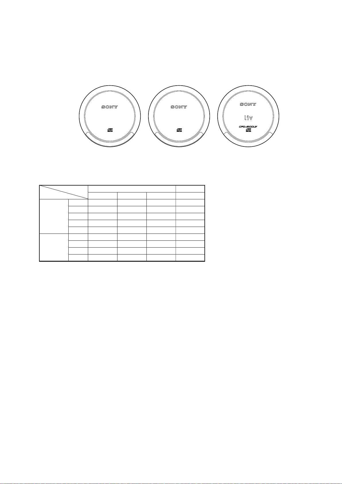
[MODEL IDENTIFICATION]
CD RADIO CASSETTE-CORDER
CFD-E100L
CD RADIO CASSETTE-CORDER
CFD-E100
CD RADIO CASSETTE-CORDER
The CFD-E100/E100L are available with three types and four different color variations.
How to identify the destination, type, and color variation is shown below.
– CD LID Top View –
CFD-E100/E100L
Ver. 1.1
CD RADIO CASSETTE-CORDER
CFD-E100
ORIGINAL TYPE
(CFD-E100)
CD RADIO CASSETTE-CORDER
CFD-E100L
ORIGINAL TYPE
(CFD-E100L)
• COLOR V ARIA TION
ORIGINAL TYPE LIV TYPE
WHITE SILVER BLUE WHITE
US a ——a
CND a ———
CFD-E100 SP — aa—
TW — aa—
KR — aa—
AEP — aa—
CFD-E100L
•Abbreviation
UK — a ——
EE, RU — a ——
IT — a ——
CND : Canadian model
EE : East European model
IT : Italian model
KR : Korean model
RU : Russian model
SP : Singapore model
TW : Taiw an model
CD RADIO CASSETTE-CORDER
LIV TYPE
(CFD-E100: US)
5
Page 6
CFD-E100/E100L
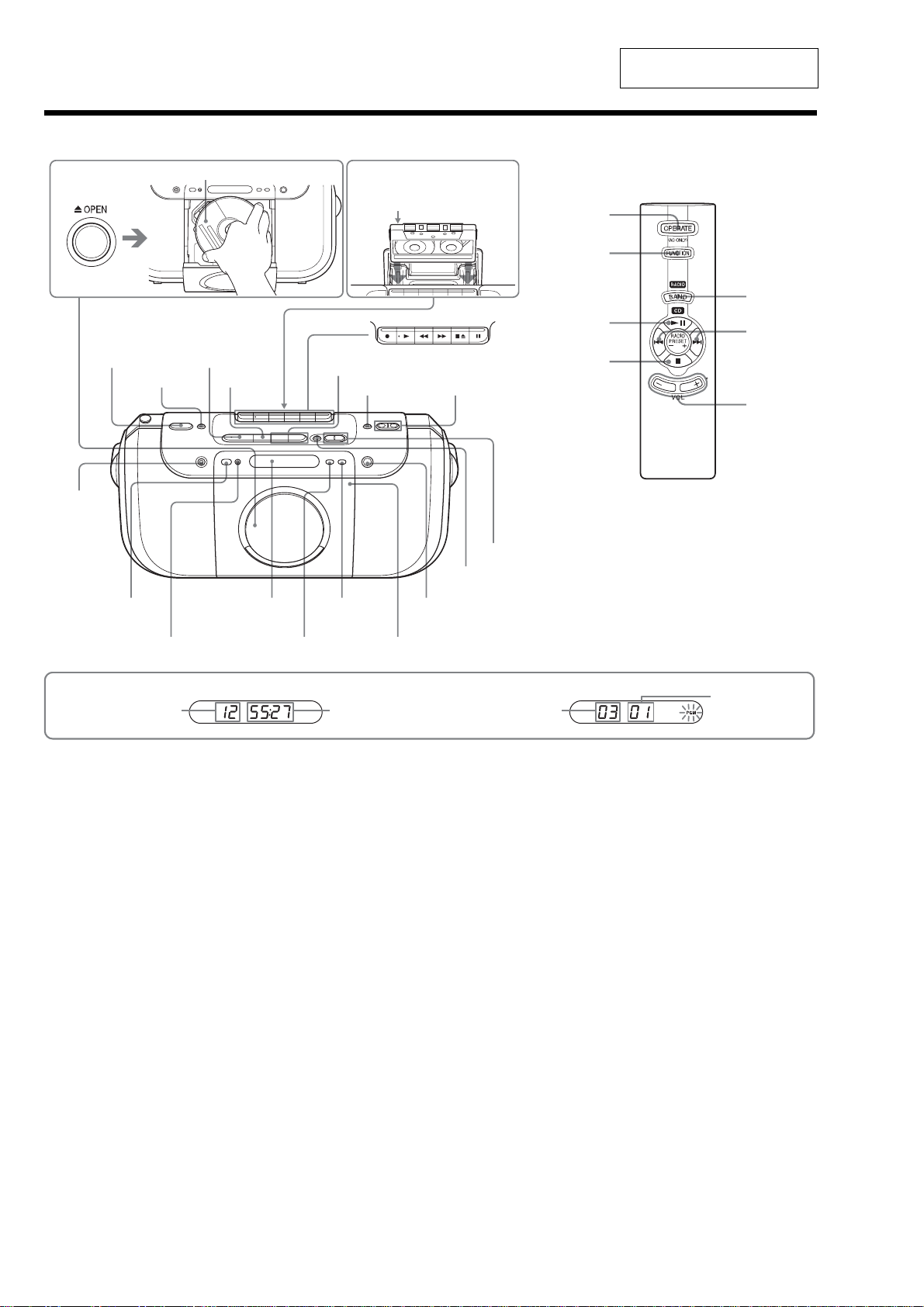
Location of controls
SECTION 2
GENERAL
This section is extracted from
instruction manual.
Loading a CD
OPERATE
(POWER)
i
Remote sensor
With the labeled side up
u*
SLEEP
Inserting a cassette
With the side you want
to play facing out
*
PRESET +, –
x
Display
.,>
MODE
MEGA BASS
Z OPEN
VOLUME +*, –
TUNE +, –
RADIO•BAND
AUTO PRESET
Remote Control
OPERATE
(POWER)
FUNCTION
u
x
*The button has a tactile dot.
BAND
PRESET +, –
.,>
VOL +*, –
Display
D
Total track number
To turn on/off the power
CFD-E100L: Press OPERATE.
CFD-E100: Press POWER.
OPR/BATT
DISPLAY
ENTER/MEMORY
Total playing time
PUSH CLOSE
E
Programmed track
Playing order
6
Page 7
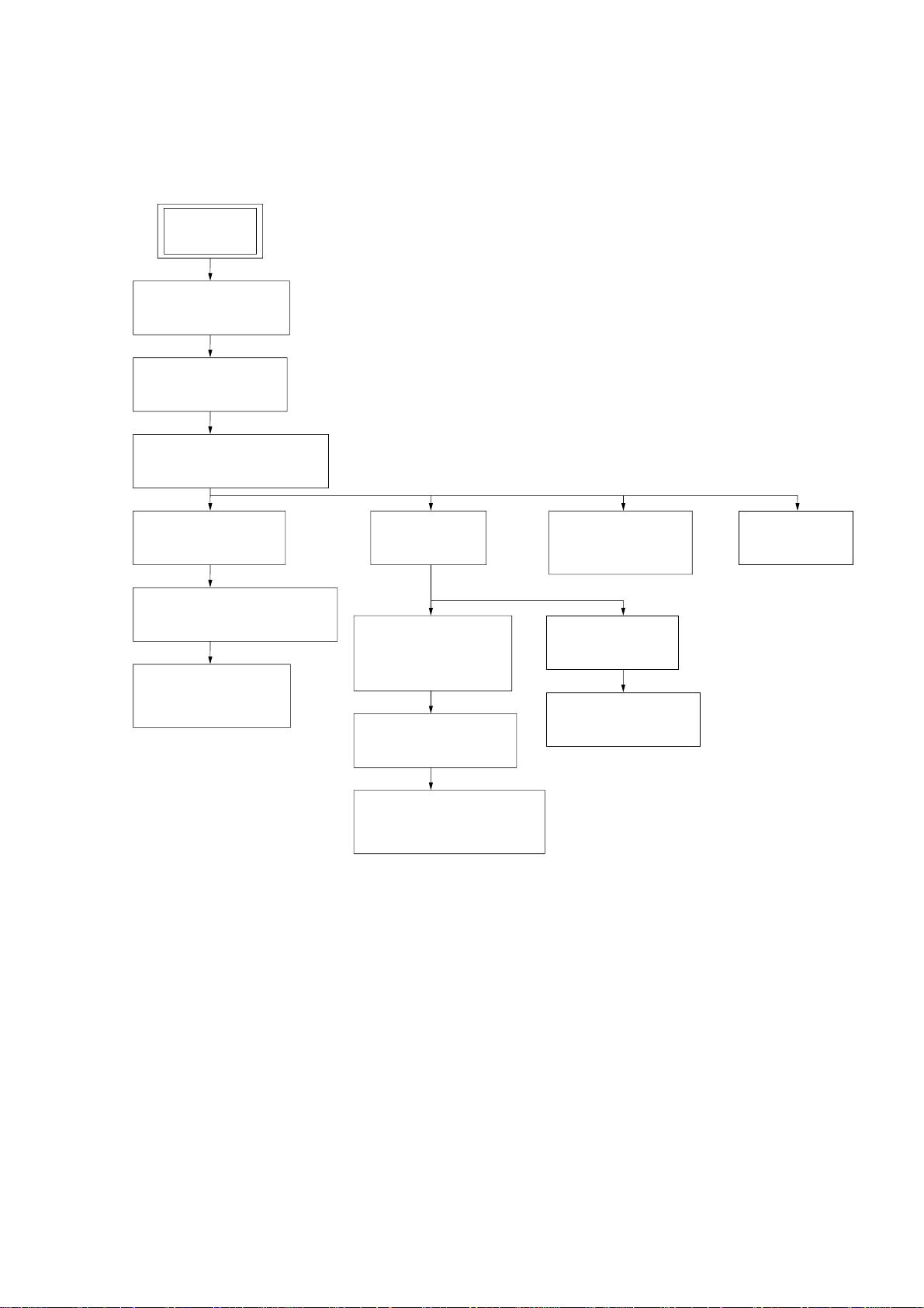
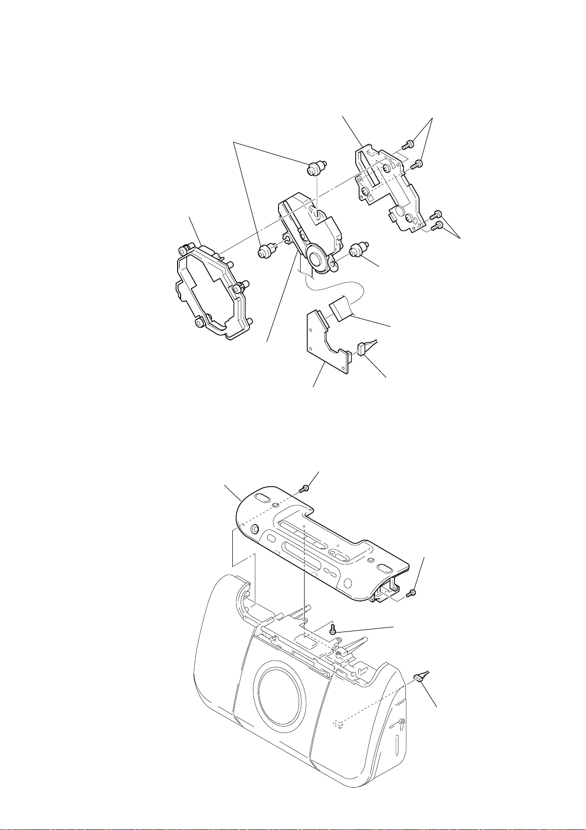
• This set can be disassembled in the order shown below.
3-1. DISASSEMBLY FLOW
SET
3-2. COVER (HANDLE)
(Page 8)
3-3. HANDLE BLOCK
(Page 8)
3-4. CABINET (REAR) BLOCK
(Page 9)
CFD-E100/E100L
SECTION 3
DISASSEMBLY
3-5. CD TRA Y BLOCK
(Page 10)
3-6. OPTICAL PICK-UP BLOCK
(Page 10)
3-7. OPTICAL PICK-UP
(KSM-900AAA)
(Page 11)
3-9. MD BLOCK
(Page 12)
3-12.TAPE MECHANISM
DECK
(MF-E100)
(Page 13)
3-13.RP HEAD (HRP301)
(Page 14)
3-14.MOTOR SUB ASSY
(CAPSTAN/REEL) (M901)
(Page 14)
3-8. PANEL (UPPER)
BLOCK
(Page 11)
3-10.MAIN BOARD
(Page 12)
3-11.POWER BOARD
(Page 13)
3-15.TU BOARD
(Page 15)
7
Page 8
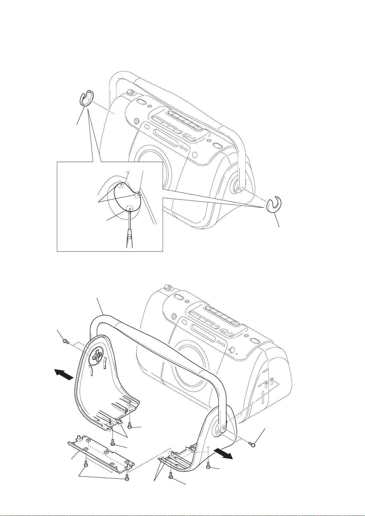
CFD-E100/E100L
s
Note: Follow the disassembly procedure in the numerical order given.
3-2. COVER (HANDLE)
3
cover
(handle)
2
two claws
3-3. HANDLE BLOCK
0
2
two screws
(B2.6)
1
claw
handle block
3
cover
(handle)
1
two screw
(B2.6)
9
panel (lower)
5
five screws
(B2.6)
8
two claws
7
screw
8
4
four screws (B2.6)
two claws
6
screw
3
four screws
(B2.6)
8
Page 9
3-4. CABINET (REAR) BLOCK
6
two screws
(B2.6)
8
two screws
(B2.6)
5
two caps (rear)
9
Open the cassette lid.
0
two screws (B2.6)
4
screw (B2.6)
CFD-E100/E100L
1
battery case lid
2
two screws
(B2.6)
7
Open the CD lid.
qf
cabinet (rear) block
3
screw
(B2.6)
qa
qd
connector
(CN362)
qs
three flexible flat cable
(21 core: CN802, 7 core: CN804, 14 core: CNP702)
9
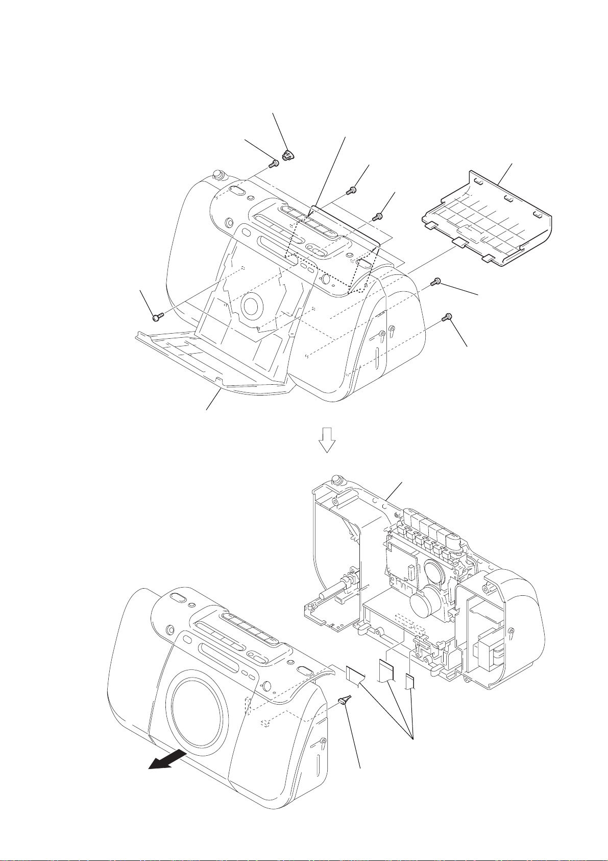
Page 10
CFD-E100/E100L
3-5. CD TRA Y BLOCK
2
4
plate (CD shaft)
two screws (B2.6)
1
flexible flat cable
(20 core) (CN P701)
2
two screws (B2.6)
3
plate (CD shaft)
6
CD tray block
3-6. OPTICAL PICK-UP BLOCK
6
optical pick-up block
5
Open the CD lid.
2
four screws
(B2.6)
1
four screws
(B2.6)
10
5
CD tray
4
screws
(B2.6)
3
cover (CD tray)
Page 11
3-7. OPTICAL PICK-UP (KSM-900AAA)
r
8
two insulators
4
frame (CD) block
3
cover (frame CD)
9
insulator
2
four screws
(B2.6)
CFD-E100/E100L
1
two screws
(B2.6)
3-8. PANEL (UPPER) BLOCK
5
panel (upper) block
0
optical pick-up
(KSM-900AAA)
7
CD relay board
4
screw
5
flexible board
(CNP705)
6
connector (CNP706)
3
screw (B2.6)
2
two screws
(B2.6)
1
connecto
(CN363)
11
Page 12
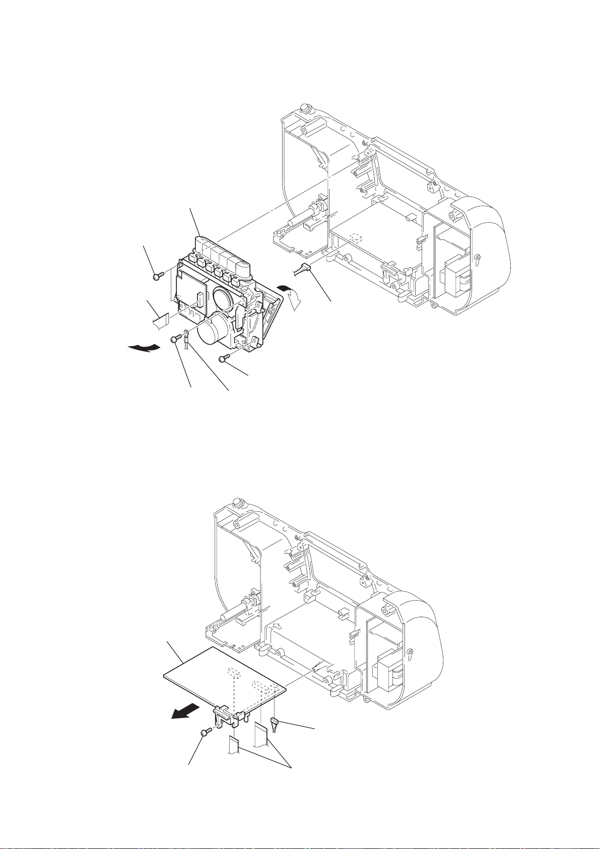
CFD-E100/E100L
3-9. MD BLOCK
7
Open the cassette lid in the direction of arrow A,
and remove the MD block in the direction of arrow
6
two screws (B2.6)
B
.
1
flexible flat cable
(13 core) (CN303)
3-10. MAIN BOARD
B
3
screw
(B2.6)
4
5
two screws (B2.6)
ground
A
connector
2
(CN311)
12
5
MAIN board
1
2
screw
(B2.6)
4
connector
(CN331)
3
two flexible flat cables
(11 core: CN801, 14 core: CN803)
Page 13
3-11. POWER BOARD
1
two harnesses
2
four screws
(B2.6)
3
POWER board
CFD-E100/E100L
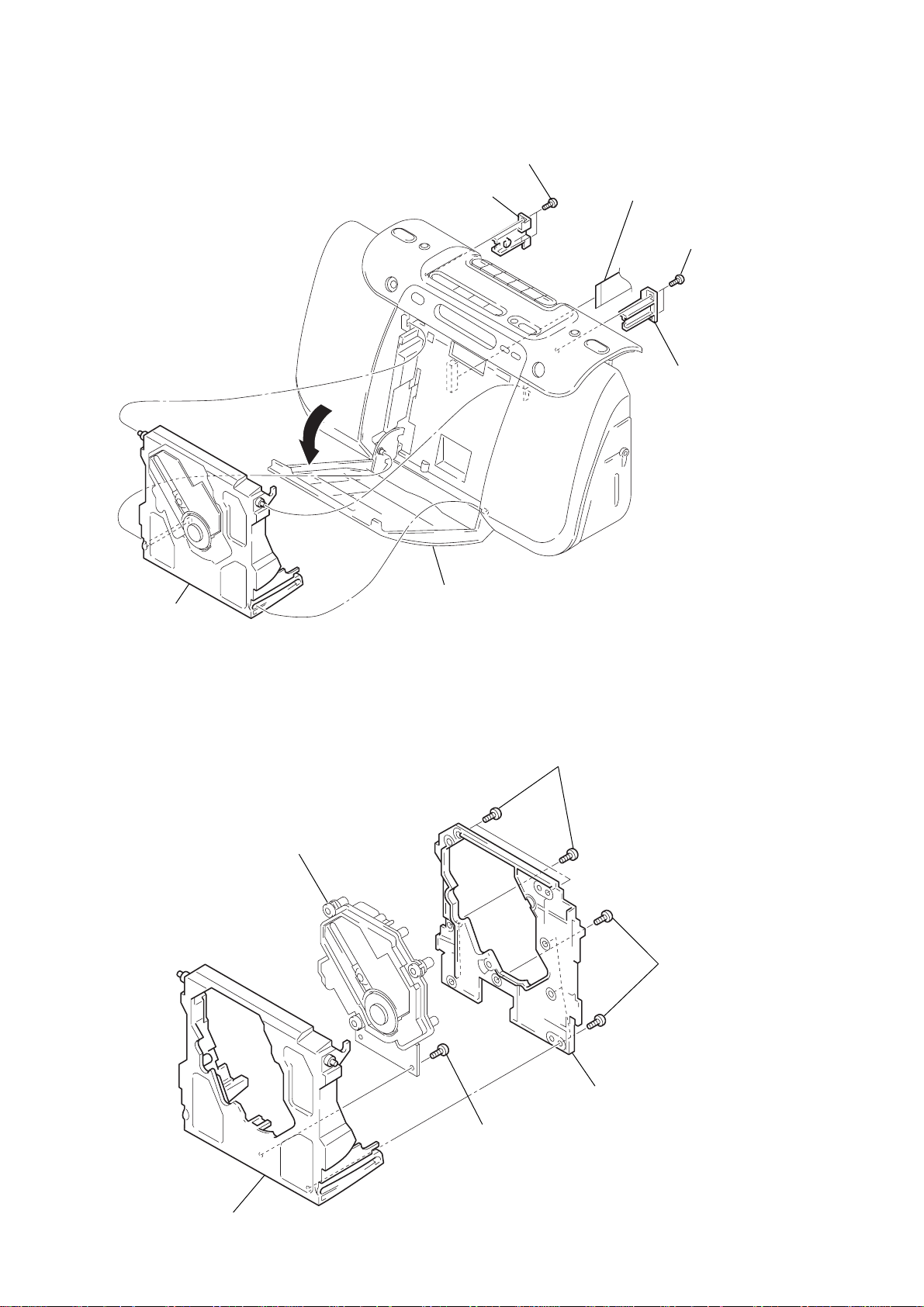
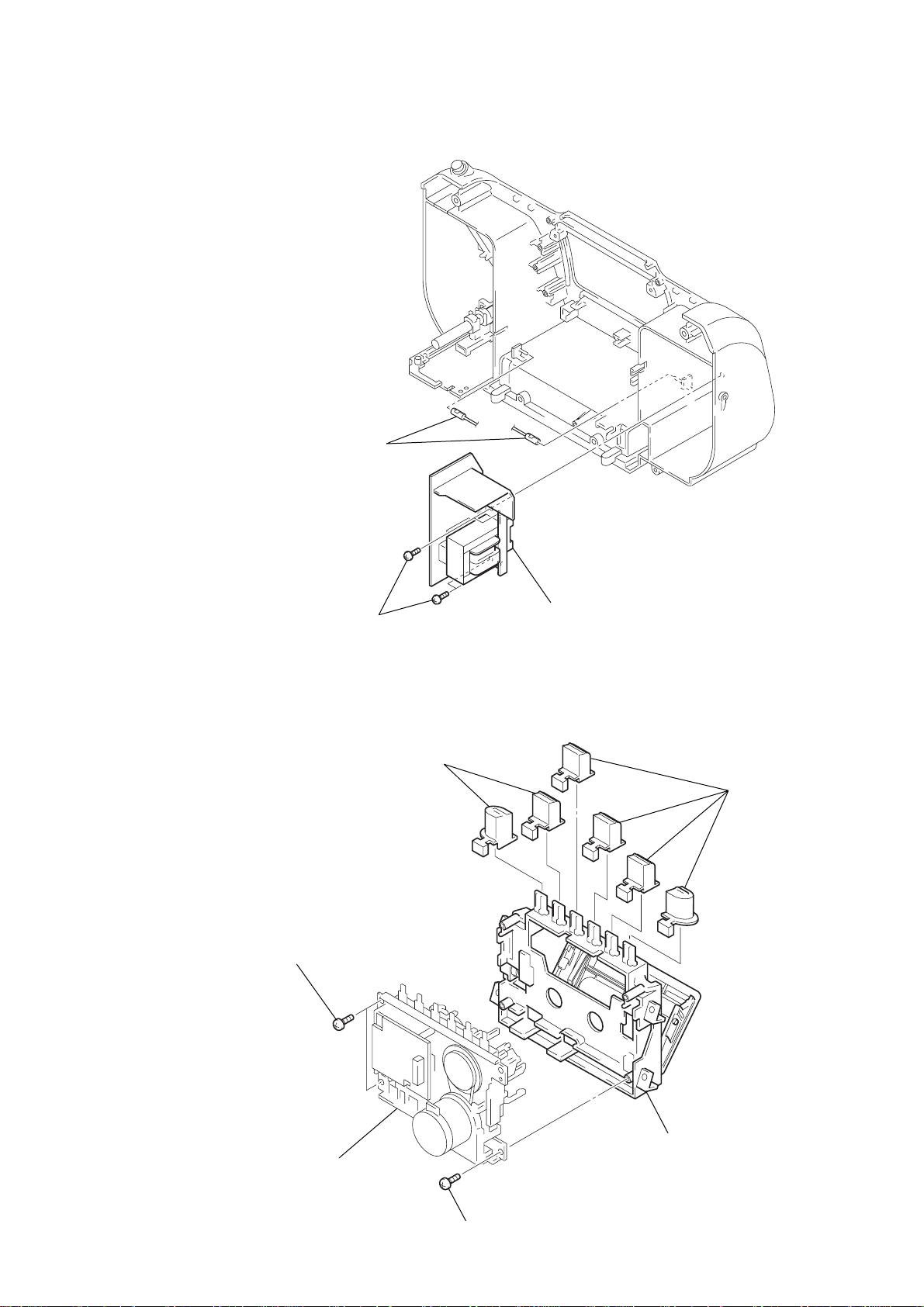
3-12. TAPE MECHANISM DECK (MF-E100)
1
two buttons
3
two screws (B2.6)
2
four buttons
6
tape mechanism deck
(MF-E100)
4
screw (B2.6)
5
cassette lid block
13
Page 14
CFD-E100/E100L
3-13. RP HEAD (HRP301)
7
RP head (HRP301)
6
two claws
4
four solders
3
2
hook
5
PRE board
1
screw
tape mechanism deck
3-14. MOTOR SUB ASSY (CAPSTAN/REEL) (M901)
3
claw
1
two solders
2
screw
tape mechanism deck
14
6
RF belt
5
main belt
4
motor sub assy
(CAPSTAN/REEL) (M901)
Page 15

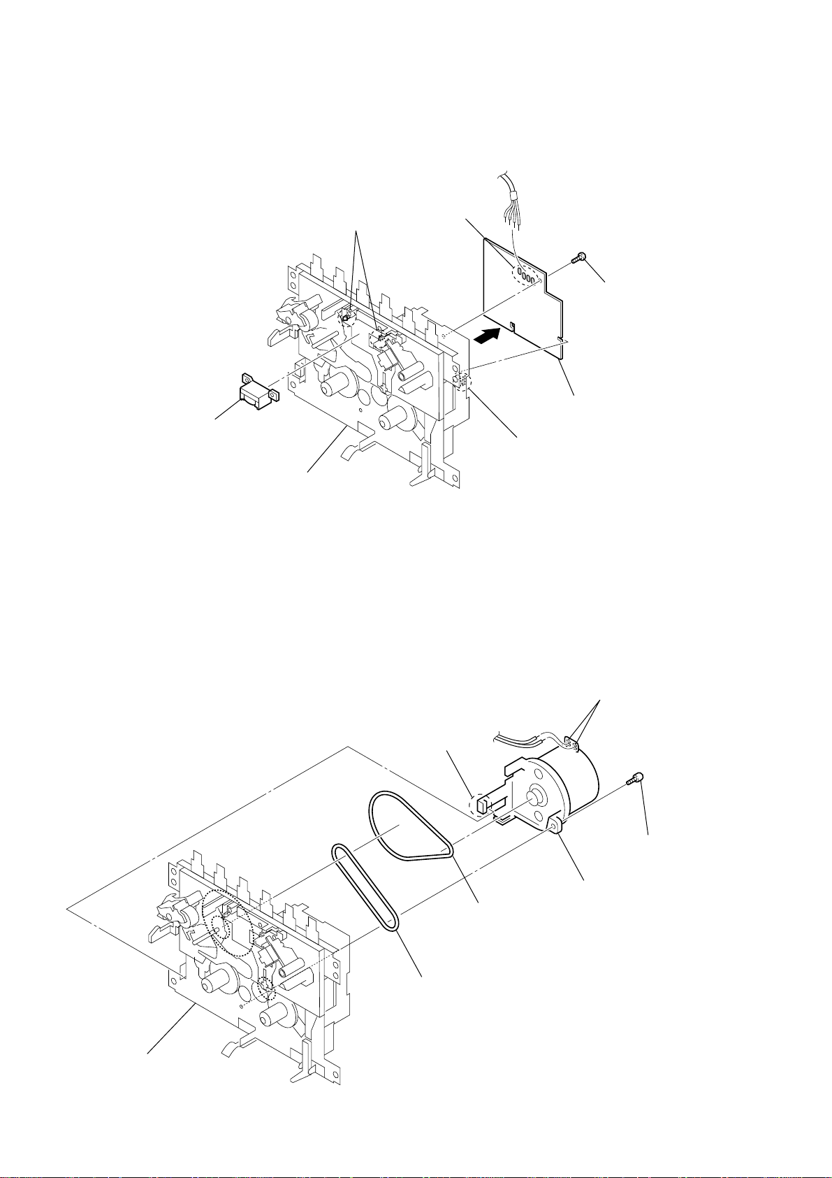
3-15. TU BOARD
CFD-E100/E100L
1
screw (B2.6)
2
4
TU board
3
flexible flat cable
(11 core) (CNP1)
15
Page 16
CFD-E100/E100L
SECTION 4
MECHANICAL ADJUSTMENTS
SECTION 5
ELECTRICAL ADJUSTMENTS
PRECAUTION
1. Clean the following parts with a denatured-alcohol-moistened
swab :
record/playback head pinch roller
erase head rubber belts
capstan idlers
2. Demagnetize the record/playback head with a head demagnetizer. (Do not bring the head magnetizer close to the erase
head.)
3. Do not use a magnetized screwdriver for the adjustments.
4. The adjustments should be performed with the rated power
supply voltage unless otherwise noted.
•Torque Measurement
Mode Torque Meter Meter Reading
FWD CQ-102C (30 – 70 g•cm)
FWD
Back Tension
FF CQ-201B (more than 60 g•cm)
REW CQ-201B (more than 60 g•cm)
CQ-102C (1.5 – 5.5 g•cm)
•Tape Tension Measurement
Mode Tension Meter Meter Reading
FWD CQ-403A
2.95 – 6.86 mN•m
(0.42 – 0.97 oz•inch)
0.15 – 5.39 mN•m
(0.021 – 0.076 oz•inch)
more than 5.89 mN•m
(more than 0.83 oz•inch)
more than 5.89 mN•m
(more than 0.83 oz•inch)
more than 100 g
(more than 3.53 oz)
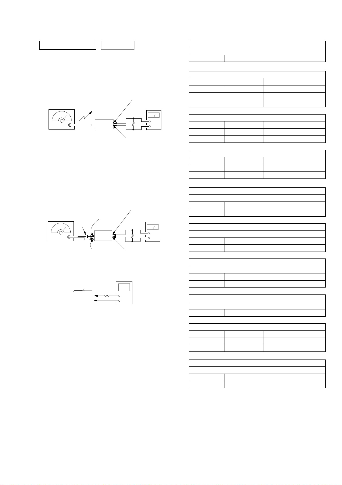
PRECAUTION
1. Setting
MEGABASS control : OFF
TAPE DECK SECTION 0 dB=0.775 V
Test tape
Type Signal Used for
WS-48B 3 kHz, 0 dB Tape Speed Adjustment
TAPE SPEED ADJUSTMENT
Setting:
Function: TAPE
HEADPHONE
TRANSLATION board
Test tape
WS-48B
(3 kHz, 0 dB)
CN361 pin
set
Procedure:
1. Playback WS-48B (tape center) in the FWD state.
2. Adjsut the volume in CAPST AN/REEL motor (M901) so that
the frequency counter reading becomes 3,000 Hz.
Specified Value: 2,910 to 3,090 Hz
3. Confirm that the frequency at the beginning and that at the
end of tape winding are between 2,940 to 3,060 Hz.
4
frequency counter
3.2
Ω
+
–
HEADPHONE
TRANSLATION board
CN361 pin
3
Adjustment Location:
– TAPE deck block –
CAPSTAN/REEL
motor (M901)
Tape speed
Adjustment
Sample Value of Wow and Flutter:03% or less W. RMS (JIS)
(WS-48B)
16
Page 17
CFD-E100/E100L
Ver. 1.1
TUNER SECTION 0 dB=1 µV
[AM]
Setting:
Function: RADIO
Band: AM
HEADPHONE
TRANSLATION board
AM RF signal
generator
30% amplitude
modulation by
400 Hz signal
Output level:
as low as possible
Put the lead-wire
antenna close to
the set.
set
CN361 pin
3.2
HEADPHONE
TRANSLATION board
CN361 pin
[FM]
Setting:
Function: RADIO
Band: FM
HEADPHONE
TRANSLATION board
FM RF signal
generator
75 kHz frequency
deviation by 1 kHz
signal
Output level:
as low as possible
TP (GND)
0.01 µF
TU board
TP (GND)
TU board
TP (VT)
TU board
TP (ANT)
set
digital voltmeter
100 k
CN361 pin
3.2
HEADPHONE
TRANSLATION board
CN361 pin
Ω
•Repeat the procedures in each adjustment several times, and
the tracking adjustments should be finally done by the trimmer
capacitors.
• Remove FM antenna in FM adjustment.
4
level meter
Ω
+
–
3
4
level meter
Ω
+
–
3
AM IF ADJUSTMENT
Adjust for a maximum reading on level meter
T1 450 kHz
( ): Singapore, Taiwan, Korean model
AM CV VOLTAGE ADJUSTMENT (CFD-E100 only)
Adjustment Part Frequency Display Reading on Digital Voltmeter
L4 530 kHz (531 kHz) 1.0 ± 0.05 V
Confirmation
LW CV VOLTAGE ADJUSTMENT (CFD-E100L only)
Adjustment Part Frequency Display Reading on Digital Voltmeter
L4 153 kHz 0.6 ± 0.05 V
Confirmation 279 kHz 5.3 ± 0.7 V
MW CV VOLTAGE ADJUSTMENT (CFD-E100L only)
Adjustment Part Frequency Display Reading on Digital Voltmeter
Confirmation 531 kHz 0.9 ± 0.4 V
Confirmation 1,611 kHz 5.2 ± 0.5 V
AM TRACKING ADJUSTMENT (CFD-E100 only)
Adjust for a maximum reading on level meter
L3 620 kHz (621 kHz)
CT3 1,400 kHz (1,404 kHz)
MW TRACKING ADJUSTMENT (CFD-E100L only)
Adjust for a maximum reading on level meter
L3-1 621 kHz
CT3 1,404 kHz
LW TRACKING ADJUSTMENT (CFD-E100L only)
Adjust for a maximum reading on level meter
L3-2 162 kHz
CT5 261 kHz
Adjust for a minimum reading on level meter
T2 10.7 MHz
Adjustment Part Frequency Display Reading on Digital Voltmeter
L2 108 MHz 3.0 ± 0.2 V
Confirmation 87.5 MHz 1.3 ± 0.3 V
1,710 kHz
(1,611 kHz)
FM IF ADJUSTMENT
FM CV VOLTAGE ADJUSTMENT
5.3 ± 0.7 V (4.8 ± 0.7 V)
( ): Singapore, Taiwan, Korean model
FM TRACKING ADJUSTMENT
Adjust for a maximum reading on level meter
L1 87.5 MHz
CT1 108 MHz
Adjustment Location: TU board (See page 18)
17
Page 18
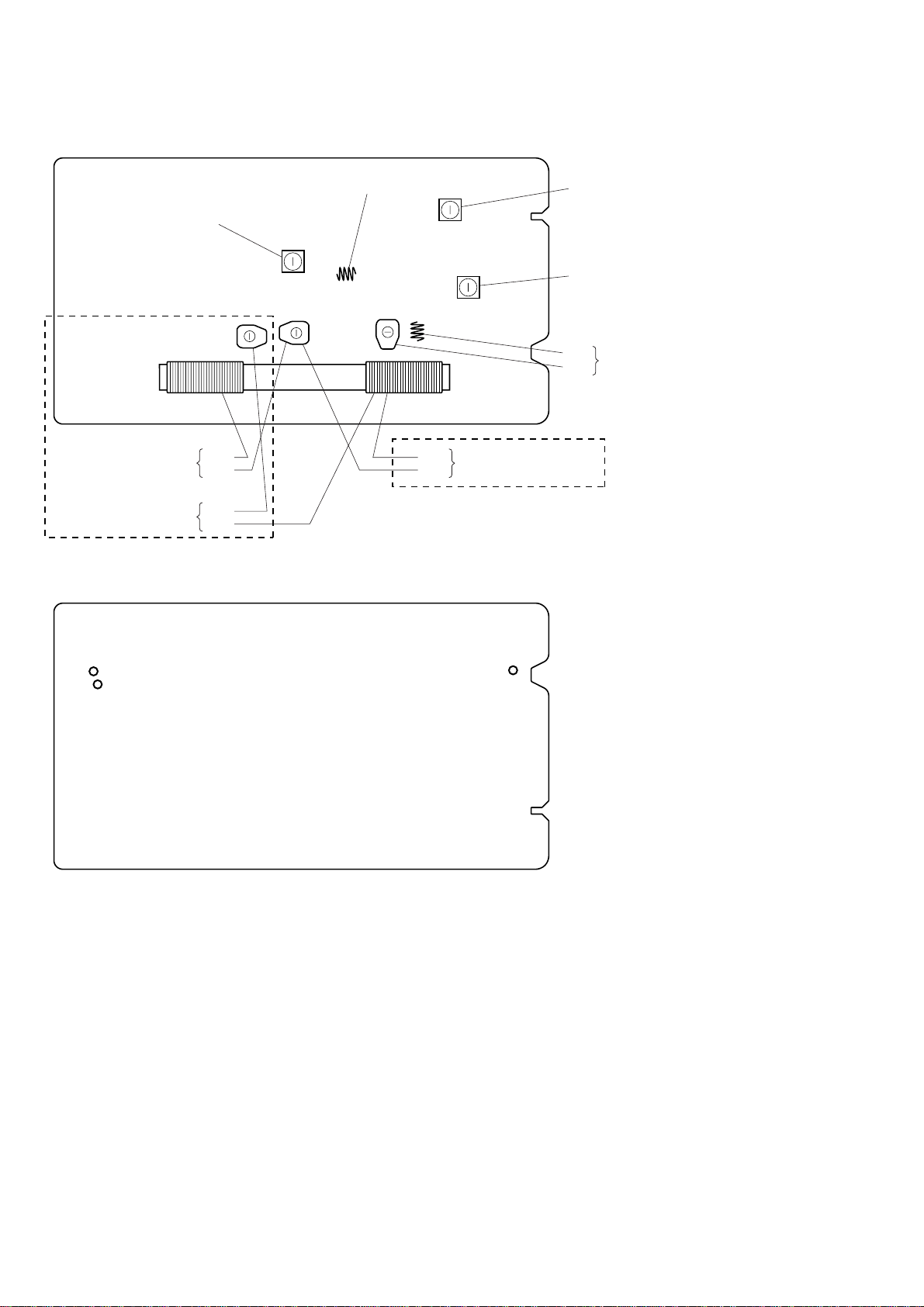
CFD-E100/E100L
Adjustment Location:
– TU BOARD (Component Side) –
L4
AM CV Voltage Adjustment (CFD-E100)
LW CV Voltage Adjustment (CFD-E100L)
FM CV Voltage Adjustment
L2
T2 FM IF Adjustment
T1 AM IF Adjustment
L1
FM T rac king Adjustment
CT1
MW T rac king Adjustment
LW Tracking Adjustment
(CFD-E100L)
L3-1
CT3
CT5
L3-2
– TU BOARD (Conductor Side) –
TP (VT)
TP (GND)
L3
AM T rac king Adjustment
CT3
(CFD-E100)
TP (ANT)
18
Page 19
CFD-E100/E100L
B
CD SECTION
Perform all CD section check in the test mode.
ENTERING THE CD TEST MODE
Procedure:
1. Insert the test disc (YEDS-18 (part No. 3-702-101-01)).
2. Press the [POWER] button to turn the power on.
3. While pressing the [DISPLAY, ENTER] and [VOLUME +] buttons,
open and close the CD lid, and release two buttons.
4. If the CD test mode is activated, all segments of the LCD light
up.
5. To release this mode, press the [POWER]] button to turn the
power off.
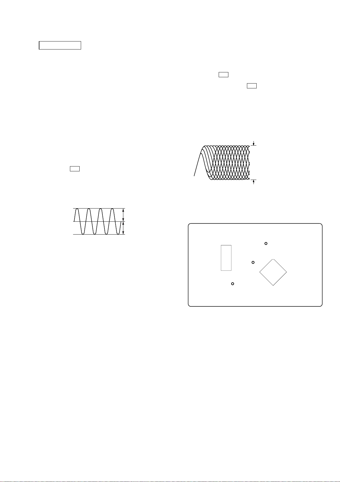
TRAVERSE CHECK
Procedure:
1. Connect an oscilloscope to TP (TE) and TP (VREF) on the
CD board.
2. Set the CD test mode.
3. Press the u button twice to display “FC”.
4. Confirm that the center of the oscilloscope waveform is at 0 V.
5. Confirm that the oscilloscope waveform Vp-p value is at 1 ±
0.5 V .
VOLT/DIV: 0.2 V (with the 10:1 probe in use)
TIME/DIV: 1 ms
A
B
A=B
Vp-p=A+
0 V
RF LEVEL CHECK
Procedure:
1. Connect the oscilloscope to TP (RF) and TP (VREF) on the
CD board.
2. Set the CD test mode.
3. Press the u button twice to display “A–”.
Note: If this check is performed continuously after the TRAVERSE
CHECK, press the u button once.
4. Confirm that the oscilloscope waveform is as shown in the
figure below. (eye pattern)
A good eye pattern means that the diamond shape (◊) in the
center of the waveform can be clearly distinguished.
• RF signal reference waveform (eye pattern)
VOLT/DIV: 0.2 V (with the 10: 1 probe in use.)
TIME/DIV: 500 ns
±
0.2 V
1.1
When observing the eye pattern, set the oscilloscope
for AC range and raise vertical sensitivity.
Connecting Location:
– CD BOARD (Conductor Side) –
TP
IC702
(RF)
TP
(VREF)
TP
(TE)
IC701
19
Page 20

CFD-E100/E100L
MEMO
20
Page 21

6-1. BLOCK DIAGRAM – SERVO Section –
CFD-E100/E100L
SECTION 6
DIAGRAMS
DETECTOR
A
D
C
B
F
E
OPTICAL PICK-UP
BLOCK
(KSM-900AAA)
LASER DIODE
PD
RF AMP, FOCUS/TRACKING SERVO,
DIGITAL SIGNAL PROCESSOR, CLV SERVO,
PD1
PD2
I-V AMP
F
E
LD
LD
AUTOMATIC
POWER
CONTROL
Q701
FIN2
8
FIN1
7
TIN2
10
TIN1
9
LDD
80
TBAL
APC
LPF
+
MIX
LPF
AUDIO
ADJUST
LDS
79
DIGITAL FILTER, D/A CONVERTER
13FE15
IC701
EQ
AGC
SW
TRACK
JUMP
S/H
TE
TDO21FDO23SLDO22SPDO
20
A/D
SW
EFMIN
3
SLISE LEVEL
CONTROL
GENERAL PURPOSE
PORTS
RUPTURE
DETECT
SERVO
PROCESSOR
RF
4
PH
BH
D/A
CONT4
25
ERROR
CORRECTION
AUDIO CD
CONT1
72
RAM
RAM
INTERPOLATION
MUTE
ATTENUATION
DEEMPHASIS
CLV, CAV
CONTROL
8FS
DIGITAL
FILTER
PLL
VCEC
COMMAND
INTERFACE
RES
WRQ
∗
∗
66
65
61CE62CL63DI64
1 BIT
DAC
AUDIO
OUT
FRAME SYNC
DETECT,
PROTECT, INSERT,
EFM DECODE
CLOCK
GENERATOR
DO
LPF
DRF
LCHO
RCHO
DOUT
FSEQ
XOUT
DRF
XIN
42
R-CH
45
39
31
48
49
67
X701
16.9344MHz
• R-ch is omitted due to same as L-ch.
• SIGNAL PATH
: CD PLAY
CD-L-OUT
58 C-FSEQ
56 C-DRF
SYSTEM CONTROLLER
IC801 (1/3)
A
(Page 23)
2-AXIS
DEVICE
(FOCUS)
(TRACKING)
PD
T+
T–
F+
F–
M701
(SLED)
M702
(SPINDLE)
S701
(LIMIT)
When the optical pick-up
ON :
FOCUS/TRACKING COIL DRIVE,
SPINDLE/SLED MOTOR DRIVE
IC702
T+
12
11
17
18
M
M
27
26
2
1
T–
F+
F–
SL+
SL–
SP+
SP–
TRACKING
COIL DRIVE
FOCUS
COIL DRIVE
SLED
MOTOR DRIVE
SPINDLE
MOTOR DRIVE
TIN
FIN
SLIN
SPIN
9
19
25
3
7MUTE
is inner position
53 C-DOUT
54 C-DIN
55 C-CLK
57 C-CE
52 C-WRQ
59 C-RST
CFD-E100/E100L
2121
Page 22

CFD-E100/E100L
6-2. BLOCK DIAGRAM – TUNER Section –
ANT1
FM TELESCOPIC
ANTENNA
FM/AM RF AMP, MIX, OSC,
FM/AM IF AMP, DET, MPX
IC1 (CFD-E100)
IC1 (CFD-E100L)
10
QUAD
T2
FM IFT
T2
FM IF
(CFD-E100)
L3
AM FERRITE-ROD
ANTENNA
L3
MW/LW FERRITE-ROD
ANTENNA
L3-1
MW
+6V
L3-2
LW
CT3, L3-1
MW
TRACKING
CT5, L3-2
LW
TRACKING
(CFD-E100L)
Q41
Q41, 42
MW ON
CT3, L3
AM TRACKING
CT5
Q42
MW/LW SWITCH
Q14
Q43
LW ON
L1
FM RF
CT1, L1
FM TRACKING
CT1
CT3
(CFD-E100)
VOLTAGE
MW/LW CV
VOLTAGE
(CFD-E100L)
X1
75kHz
L4
AM CV
L4
D3
(1/2)
111218
AM IN
FM
IF-IN
FM IF
AMP
AM
IF-IN
AM IF
6
AMP
FM
DET
AM
DET
IF
BUFFER
IF-OUT
17 18
AF
BUFFER
LEVEL
DET
DET
-OUT
ST
IND
ST-IND
MPX
-IN
AF
16
MW/LW
HIGH CUT
Q12
15
AMP
MPX
LPF1/BAND
LPF2/MO-ST
13
14
MUTE
STEREO/
MONO,
FM/AM
L-OUT
R-OUT
12
11
R-CH
TU-L-OUT
B
(Page 23)
• R-ch is omitted due to same as L-ch.
• SIGNAL PATH
: FM
: AM (MW/LW)
R DATA, R CLOCK, R CE,
R COUNT, R MUTING
D
(Page 23)
10 9
IF IN
UNIVERSAL
COUNTER
ST-IND
BAND
7
BAND
13817 16
MO/ST
CCB
INTERFACE
MUTING
Q801
DI
CL
CE
DO
R MUTING
2
3
1
4
R DATA
R CLOCK
R CE
R COUNT
FM
RF-IN
FM
RF-OUT
AM
RF-IN
L4
AM
OSC
REFERENCE
DIVIDER
FM
RF AMP
AM
RF AMP
D3
(2/2)
2
24
D1
22
XOUT
20
XIN
19
FM
MIX
FM
OSC
AM
MIX
AM
OSC
AM OSC
20 21
(CFD-E100L)
FM OSC
Q44
LW ON
6
MW/LW
BUFFER
BUFFER
LP-OUT
MIX-OUT
D2
LOW-PASS
FILTER
LOW-PASS
FILTER
UNLOCK
DETECT
4 7
AM IFT
T1
AM IF
OSC
-OUT
19
L2
FM CV VOLTAGE
L2
FM OSC
(CFD-E100)
CONSTANT
CURRENT
Q61
(CFD-E100L)
PD
LP-IN
PHASE
DETECTOR/
CHARGE PUMP
12 BIT
PROGRAMMABLE
DIVIDER
T1
CF2
CF4
VT
SWALLOW
COUNTER
FM IN
1/2
CFD-E100/E100L
FM/AM PLL
IC2 (CFD-E100)
IC2 (CFD-E100L)
SHIFT REGISTER & LATCH
2222
Page 23

6-3. BLOCK DIAGRAM – AUDIO Section –
CFD-E100/E100L
(Page 21)
(Page 22)
A
B
CD-L-OUT
TU-L-OUT
L-CH
R-CH
HRP301
(REC/PB)
HE301
(ERASE)
S301 (2/2)
(REC/PB)
RECPB
Q302
VREF
R-CH
T301
BIAS OSC
Q303
INPUT SELECT,
REC/PB PRE AMP
VREF
13
24
22
5
4
6
Q302, 303
ISS SWITCHING
IC301
MIC IN
L.CD
L.RAD
L.IN
L.RO
VREF
BIAS OSC
Q301
PB
EQ AMP
BUFFER
REC
EQ AMP
DET
REFERENCE VOLTAGE
GENERATOR
S301 (1/2)
(REC/PB)
ALC
RECPB
MIC
AMP
TC 6V
MUTE
R-CH
BUFFER
LOGIC CIRCUIT
LINE
TAPE
REC
17 15 21
MUTE
MONITOR
AMP
L.LO
+9V
8
POWER
AMP
ST-BY
IC351
ELECTRICAL VOLUME
IC331
R-CH
LOGIC
CLK
L-OUT
7
MUTING
Q151
R-CH
LIN
20
8
CONTROL
DATA
4 5
L-IN
11
MEGA BASS
CONTROL
Q131
STANDBY
SWITCH
POWER
AMP
R-CH
L-OUT
5
D351
D331
R-CH
SP101
(L-CH)
SP201
(R-CH)
J361
i
R-ch is omitted due to same as L-ch.
SIGNAL PATH
: CD PLAY
: TUNER (FM/AM)
: TAPE PLAY
: REC
(Page 24)
(Page 22)
CD-ON
C
37CD36
TAPE
27
REC
SYSTEM CONTROLLER
IC801 (2/3)
66
D
R MUTING
R DATA
R CLOCK
R CE
R COUNT
65
62
63
64
61
R-MUTE
R-DATA
R-CLK
R-LAT
R-COUNT
ISS1
67
ISS2
78 77 35
V-CLK
V-DATA
A-MUTE
68
M-BASS
CFD-E100/E100L
2323
Page 24

CFD-E100/E100L
6-4. BLOCK DIAGRAM – PANEL, POWER SUPPLY Section –
LIQUID CRYSTAL
DISPLAY
LCD401
S0 – S16
10 – 26
COM0 – COM3
6 – 9
S407 – 414
S401 – 406
REMOTE CONTROL
RECEIVER
IC401
D801
WAKE UP
SWITCH
Q803
MODE CHECK
SWITCH
Q802
X802
4.19MHz
X801
32.768kHz
EEPROM
IC803
REMOTE
48
KEY2
44
KEY1
45
WP/INI
50
MODE CHK
46
75
X2
74
X1
71
XT2
70
XT1
80
SDA
79
SCL
SYSTEM CONTROLLER
IC801 (3/3)
3V-CHK
CD6V-CHK
6V-CHK
9V-CHK
P-CON
VLC0
VLC1
VLC2
RST
42
CD +3.3V
40
41
43
60
5
4
3
76
POWER CONTROL
Q905
RESET SIGNAL
GENERATOR
IC802
D932 (2/2)
D931
D932 (1/2)
+3.3V
REGULATOR
Q908
+6V
REGULATOR
CONTROL
Q906, 907
CD +6V
+6V
REGULATOR
Q904
VT
+9V
VCC +3.3V
D951
REGULATOR
REGULATOR
VCC +9V
+6V
Q903
B+ SWITCH
Q901, 902
+3.3V
IC901
CD-ON
C
(Page 23)
CFD-E100/E100L
S701
(CD LID OPEN/CLOSE)
S903
(MOTOR ON/OFF)
M901
(CAPSTAN/REEL)
S902
(TAPE PLAY)
29
CD DOOR
+9V
RMC B+
M
49
TC-PLAY
AC-CHK
28
AC CHECK
Q804
D941
RECT
D901 – 904
DRY BATTERY
SIZE "C"
(IEC DESIGNATION R14)
6PCS. 9V
POWER
TRANSFORMER
T901
F901
J901
- AC IN
2424
Page 25

CFD-E100/E100L
Ver. 1.1
• Note for Printed Wiring Boards and Schematic Diagrams
Note on Printed Wiring Board:
• X : parts extracted from the component side.
• Y : parts extracted from the conductor side.
• W : indicates side identified with part number.
f
•
• : Pattern from the side which enables seeing.
: internal component.
Note on Schematic Diagram:
• All capacitors are in µF unless otherwise noted. (p: pF)
50 WV or less are not indicated except for electrolytics
and tantalums.
• All resistors are in Ω and 1/
specified.
• f : internal component.
• C : panel designation.
Note:
The components identified by mark 0 or dotted line with mark 0 are
critical for safety.
Replace only with part
number specified.
• A : B+ Line.
• H : adjustment for repair.
• Power voltage is dc 9V and fed with regulated dc power
supply from battery terminal.
– CD Section –
[]: CD PLAY
– TUNER Section –
no mark : FM
(): AM (MW)
< >: LW
– Other Section –
no mark : TUNER
(): CD PLAY
〈〈 〉〉 : T APE PLAY
[]: REC
• Voltages are taken with a V OM (Input impedance 10 MΩ).
Voltage v ariations may be noted due to normal production
tolerances.
• Waveforms are taken with a oscilloscope.
Voltage v ariations may be noted due to normal production
tolerances.
• Circled numbers refer to waveforms.
• Signal path.
F : FM
f : AM (MW/LW)
J : CD PLAY
E : TAPE PLAY
a : REC
•Abbreviation
CND : Canadian model
EE : East European model
IT : Italian model
KR : Korean model
RU : Russian model
SP : Singapore model
TW : Taiwan model
4
W or less unless otherwise
Note:
Les composants identifiés
par une marque 0 sont critiques pour la sécurité.
Ne les remplacer que par une
piéce portant le numéro
spécifié.
• Circuit Boards Location
TU board
BATTERY 2 board
HEADPHONE board
MAIN board
CD board
HEADPHONE TRANSLA TION board
POWER board
BATTERY 1 board
LCD board
CFD-E100/E100L
REMOTE CONTROL board
CD RELAY board
MODE board
PRE board
2525
Page 26

CFD-E100/E100L
6-5. PRINTED WIRING BOARDS – CD Section –
1 2 3 4 5 6 7
CD RELAY BOARD
A
JW762
B
1
JW761
20
CNP706
6
1
1-866-171-
11
(11)
C
M701
M
(SLED)
ON: WHEN THE OPTICAL PICK-UP
IS INNER POSITION
S701
(LIMIT)
M
M702
(SPINDLE)
D
• See page 25 for Circuit Boards Location. :Uses unleaded solder.
CD BOARD
Q701
C701
JC707
CNP705
OPTICAL PICK-UP
BLOCK
(KSM-900AAA)
R741
R746
JW723
JW722
CNP701
2
JW717
JC706
20
JW715
JW724
1
19
R712
JW725
JW720
C751
JW726
JW727
JW721
JC705
JW718
JW719
R707
JC704
IC702
JC711
C733
C702
JC703
R744
JW716
TP
(VREF)
JW712
JW713
JW711
C741
C707
C706
JW729
C740
C708
R740
R742
R704
(TE)
JC708
JW710
JW708
JC709
TP
JW730
R715
C742
JW709
R714
C736
R723
R706
20
21
R702
R703
C734
JW731
JW732
TP
(RF)
JW707
C704
R708
C743
C727
R709
C705
C731
C703
180
IC701
40 41
C709
JW706
R710
R713
R711
C711
R729
C744
C716
JW705
R730
C745
JC710
JW704
R728
C730
JW733
C746
C717
R747
FB701
R727
61
60
R726
R722
C721
R724
R721
R739
R725
R720
C720
X701
C735
JW734
R731
C723
C725
R719
R717
JW703
R718
R716
R751
R750
C724
C722
C755
R732
C728
L706
C729
C726
JW702
C754
R748
R733
CNP702
2
14
8
1
13
1-687-668-
A
MAIN
BOARD
CN803
(Page 33)
11
(11)
CFD-E100/E100L
2626
Page 27

CFD-E100/E100L
6-6. SCHEMATIC DIAGRAM – CD Section –
SP-
SP+
LIM
GND
SL-
SL+
LD
PD2
F
PD1
VC
E
GND
VCC
VR
PD
T+
F+
F-
T-
CNP701
SP-
SP+
LIM
GND
SL-
SL+
PD2
PD1
GND
VCC
20P
LD
F
VC
E
VR
PD
T+
F+
F-
T-
JC711
SP-
SP+
LIM
SL-
C733
SL+
PD2
PD1
100
R712
100
10V
LD
F
E
PD
0
JC706
0
T+
F+
F-
D
N
G
P
S
• See page 40, 41 for IC Block Diagrams. • See page 39 for Waveforms.
CNP706
6P
SL+
SL-
GND
LIM
SP+
SP-
CNP705
16P
GND
PD2
F
PD1
E
VC
VCC
NC
LD
GND
PD
VR
F+
T+
T-
F-
PD2
PD1
R740
L
S
IN
P
S
KTN2907AS-RTK
AUTOMATIC
POWER
CONTROL
O
D
L
S
IN
L
S
T
S
R
R742
R714
R715
Q701
)
IN
L
(S
-B
G
E
R
E
F
LD
-
+
L
S
SL
+
L
S
+
P
S
ON:WHEN THE OPTICAL PICK-UP IS
10k
R702
10k
R704
220k
470k
470k
220k
R707
10
F
C
E
C
R
V
V
E
O
T
G
U
E
M
R
M701
(SLED)
S701
(LIMIT)
INNER POSITION
(SPINDLE)
C
C
V
D
N
G
M702
1000p
FDO
GND
VCC
NC
C746
C745
C744 R724
0.1 47k
C731
0.047
R709 R710
F-
C742
0.1
C743
0.1
C751
0.1
F+
+
F
F
+
T
T
22k 4.7k
C703
0.1
C704 R711 R713
22p 220 100
C706
1 50V
C708 C736
100p 4700p
C702
47
10V
C701
)
IN
IN
F
(F
)
IN
IN
T
(T
100
0.1
10V
R708
10k
C705
(RF)
4700p
4.7k
R703
4.7k
R706
(VREF)
4700p (FE)
C734
C707
1
C
IN
N
P
O
T
IC702
U
BA5826FP
D
O
N
P
G
O
JC708
(TE)
0
TDO
FDO
SPDO
SLDO
CONT4
F
E
LD
PD
G
S
IN
U
K
C
C
O
A
F
R
T
PD
R730
1k
R729
220
D
D
L
SLCO
SLCIST
EFMIN
RF
RFVDD
RFVSS
FIN1
FIN2
TIN1
TIN2
VREF
REFI
FE
TEC
TE
RFMON
JITTC
ADAVDD
ADAVSS
TDO
O
D
F
R746
4.7k
B
D
A
2
R731
2.2k
3
5
S
T
D
S
N
V
D
O
V
C
I1
I2
Q
N
E
O
IN
S
M
F
M
R723 C727
100 1000p
8
Z4
Z
Z
1k
100
100
R721
R720
R722
F
S
R
E
D
R
*
I3
I4
N
N
O
O
M
M
Z6
Z3
Z7
Z5
C726
1000p
C725
1000p
C724
22p
1k
1k
1k
100
R716
R718
R717
R719
C723
0.01
C722
22p
C721
22p
C720
22p
I
L
E
O
Q
D
C
C
D
R
W
*
I5
N
O
M
DATA
DATACK
LRSY
ASDFIN
ASDACK
ASLRCK
16MOUT
EFLG
C2F
XVSS
FSX/16MIN
XIN
XOUT
XVDD
RVDD
RCHO
RVSS
LVSS
LCHO
S
S
LVDD
T
)V
U
V
D
O
D
.3
TEST
V
D
(3
C709 C716 C711
0.1 0.01 0.01
R747
22k
C735
1000
6.3V
R751
2.2k
R739
1k
FB701
JC710
0
R750
100
C755 C754
0.01 0.01
X701
16.9344MHz
0
R748
100
C717
0.01
Z9
Z10
C740
C741
470
0.1
10V
Z1
Z2
Z3
Z4
Z5
Z6
Z7
Z8
Z9
Z10
L706
0
CNP702
14P
PGND
6V
FSEQ
DRF
DOUT
WRQ
CL
CE
DIN
XRT
CD-R-OUT
CD-L-OUT
GND
3.3V
(Page 34)
C
R728
10k
R727
2.2k
C730
0.1
T
S
R
D
F
D
D
IS
L
V
K
V
C
P
C
4
A
T
O
O
D
N
D
D
P
P
L
O
S
S
G
C
0
JC709
LIM
C728C729
0.0471
R733 R732
220 220
R725R726
470470
2
1
1
2
JC704
S
S
V
V
5
T
N
O
C
T
T
O
O
N
N
D
D
O
O
P
P
C
C
RF AMP,FOCUS/TRACKING SERVO,
DIGITAL SIGNAL PROCESSOR,
CLV SERVO,DIGITAL FILTER,
D/A CONVERTER
IC701
LC78646E
6
T
N
O
G
T
/C
/F
C
K
K
E
P
C
C
F
E
B
B
/*
S
S
V
D
0
Z1
CFD-E100/E100L
0
JC707
O
D
P
-
+
SP
SP
CONT4
S
JC705
0
R741
10k
R744
100k
JC703
0
TDO
FOCUS/TRACKING
COIL DRIVE,
SPINDLE/SLED
MOTOR DRIVE
T+T-T-
2727
Page 28

CFD-E100/E100L
6-7. PRINTED WIRING BOARD – TUNER Section (CFD-E100 Only) –
1 2 3 4 5 6 7 8 9 10
TU BOARD
A
B
JW14
TP (GND)
1
C
B1
MAIN
BOARD
CN801
(Page 33)
11
• See page 25 for Circuit Boards Location. :Uses unleaded solder.
L3
AM FERRITE-ROD
ANTENNA
(EXCEPT
(US, CND)
JC24
TP (CV)
(SHIELD CASE)
L2
C13
US, CND
(US, CND)
ANT1
FM TELESCOPIC
ANTENNA
)
L1
R5
T1
TP
(ANT)
D
E
IC2
L4
IC1
T2
C78
C77
(EXCEPT
US, CND
)
1-863-438-
11
(11)
• Semiconductor
Location
Ref. No.
D1 B-7
D2 C-6
D3 C-6
D10 B-9
D11 B-9
IC1 D-7
IC2 D-3
Location
CFD-E100/E100L
2828
Page 29

6-8. SCHEMATIC DIAGRAM – TUNER Section (CFD-E100 Only) –
CFD-E100/E100L
Ver. 1.1
• See page 41, 42 for IC Block Diagrams. • See page 39 for Waveform.
EXCEPT
US, CND
JC24
L3
AM FERRITE-ROD
ANTENNA
L11
0
(US, CND)
00
C32
1000p
R32
100k
D1
KV1471E
C34
0.01
JC12 JC11
1µH
CT3
CT1
L1
FM
RF
OSC
L2
FM
D3
KV1520NT
0.01
(US, CND)
C13
0.010.01
C41
220p
C42
100p
C43
22p
C47 C39R40R41 C49
10p 0.1220k10k
C37
0.01
R30
22k
D2C33C35
KV1471E0.01
R33
R31
4.7k
10k
C80
0.01
C31C30
22p0.01
JC3
0
R24
220
CV
FM/AM RF AMP,MIX,OSC,
FM/AM IF AMP,DET,MPX
IC1
TA2149BN
FM
GND1FMRF-IN
RF-OUT
VCC1
AM
RF-IN
FM OSC
W
O
L
T
U
M
A
C
OUT
MIX-
AM OSC
VCC2
OSC-
AM
OUT
IF-IN
FM
L4
AM OSC
C24 C22
220p 0.1
IF-OUT
ST-IND
GND2
IF-IN
TP (CV)
R11
2.2k
C23
1
50V
DET-OUT
AGC
CV
TP
(VT)
R50
1k
R91
220
R14
1k
C20
0.1
C21
1
50V
C51 C52 R51
22p 10p 10k
X1
75KHz
R52 C53
00.22
R55
C59 R53 C95
10k
100p 4.7k 1000p
C65
R65 R63
4.7
10k 10k
50V
100p
C54
220
10V
R54
470
C55
1000p
1000p
C57
C56
11
T
D
D
/S
V
O
M
D
D
AN
T-IN
B
S
IN
IN
M
FM
A
IF IN
FM/AM PLL
IC2
LC72137M-TLM
D
AN
B
MPX-IN
QUAD
T
U
LPF2
LPF1
/BAND
/MO-ST
R-OUT
L-OUT
O
X
E
C
T
IN
U
X
I
D
-IN
P
-O
L
P
L
O
L
D
C
S
D
S
P
V
W
E
/L
T
U
W
M
M
ANT1
FM TELESCOPIC
ANTENNA
(ANT)
TP
D11
1SS355
D10
1SS355
R2
470
C1
47p
R3
10k
C10
C8
1
50V
JC13
0
T1
AM IFT
CF4
JC6
0
R5
R1
470
1k
C11C4
0.11000p1000p
C18
220
10V
C12
4.7
50V
C61 C62 C63
C7
C9
10p
5p
T2
FM
IFT
CF2
C15
EXCEPT
0.01
US, CND
(US, CND)0.022
C14
EXCEPT
0.01
US, CND
(US, CND)0.022
EXCEPT
US, CND
C78
4700p
C77
4700p
JC4
R92
JC33
0
220
0
JC2
JC34
100p 100p 100p
0
0
R61 R60 R59 R58
2.2k 2.2k 2.2k 2.2k
47
R10
C29
100
10V
C27 C26
100p 100p
C66 C68
100p 100p
JC1
0
1000p
C60
R94
1k
TP
(GND)
R4
JC5
0
10k
R13
1k
R56
220
R57
100
L21
10µH
R-MUTE
R-COUNT
R-CLOCK
R-DATA
TU-LCH
TU-RCH
S-GND
R-LAT
TU-6V
CNP1
11P
B1
MAIN
GND
(Page 34)
VT
CFD-E100/E100L
2929
Page 30

CFD-E100/E100L
6-9. PRINTED WIRING BOARD – TUNER Section (CFD-E100L Only) –
A
B
C
D
E
1
TU BOARD
B2
MAIN
BOARD
CN801
(Page 33)
JW
2
R63
14
TP (GND)
C58
R10
JC1
CNP1
R61
R60
R59
R58
JC33
JC34
3 4 5 6 7 8 9 10 11
Q14
R42
R16
R22
C5
R18
R56
X1
R93
L21
C62
JW
C63
Q61
R13
R66
3
R94
C61
C64
C60
C29
R64
C51
R19
R17
R57
C52
IC2
C68
C66
F
• See page 25 for Circuit Boards Location. :Uses unleaded solder.
L3
FERRITE-ROD ANTENNA
/LW
MW
C2
R9
JC2
R50
C55
C59
C57
R4
Q41
C6
R53
(CV)
R52
C53
C95
TP
R51
C3
R54
JC5
JW5
C37
JW4
C54
R55
R91
CT5
Q44
JW6
JC4
R7
C71
JC22
Q43
C48
C73
R40
C44
C72
C70
C39
Q12
C93
JW7
R12
R43
C41
C40
L3-2
L3-1
C49
CT3
C42
C25
C45
C21
R11
C43
JC3
R14
L4
JW9
R30
C46
C22
D2
C30
C56
Q42
D3
R41
C33
L2
C31
R24
C24
C23
C20
JW10
R31
R92
C77
JW
R33
R32
JC24
8
C32
C14
C78
CT1
IC1
C80
C15
C11
D1
R2
C34
C12
C35
C7
C9
L1
C1
C18
C4
JW12
JC23
JW11
T2
CF4
JW13
C8
R3
D10
CF2
ANT1
FM TELESCOPIC
ANTENNA
D11
TP (ANT)
JW2
C10
T1
R1
JC6
1-863-438-
11
(11)
CFD-E100/E100L
• Semiconductor
Location
Ref. No.
D1 C-8
D2 D-7
D3 C-7
D10 B-9
D11 B-10
IC1 D-8
IC2 E-4
Q12 E-6
Q14 B-4
Q41 B-4
Q42 C-7
Q43 B-5
Q44 C-5
Q61 C-3
Location
3030
Page 31

CFD-E100/E100L
6-10. SCHEMATIC DIAGRAM – TUNER Section (CFD-E100L Only) –
R43
Q42
C45
C32
C46
L3
FERITE-ROD
C35
L1
JC24
CT3
C48
FM CV
VOLTAGE
R32
R16
C33
CT5
Q43
C3
TP (CV)
R30
R31
C30
R33
L2
Q41
R42
D1
CT1
C34
0
D3
C73
R41
D2
C31
C49
R40
R24
C80
JC3
C41
C42
C43
0
• See page 41, 42 for IC Block Diagrams. • See page 39 for Waveform.
Q14
C39
L4
R91
LW CV
VOLTAGE
C51
11
IC B/D
R22
R19
R17
JC22
0
C20C22
C61 C62 C63
X1
R50
R9
C72
C71 C44
Q44
R18
C25
C70 C40
C6C5
C2 C37
R7
Q12
C24
C23
R12
R14
R11
C21
SWITCH
C93
C52
R52
R59R60R61
C59
R58
C53
R51
LC72137M-TLM
R66
R55
R53
IC2
FM/AM PLL
C64
R92
C55
C95
C54
R54
R94
R93
C56
C57
C60
C68
C66
R13
JC5
0
R4
ANT1
FM/AM RF AMP,
MIX,OSC,
FM/AM IF AMP,
DET,MPX
IC B/D
TP (ANT)
D10
D11
JC4
0
IC1
JC2
0
JC33
C11
C1
R2
R3
C8
C4
C10
JC23
R1
T1
0
CF4
JC6
0
CF2
C12
C18
C7
T2
C78
C77
C14
C15
C9
0
JC34
0
R10
C29
CONSTANT
CURRENT
Q61
JC1 0
TP (GND)
R56
R57
L21
Q61
C58
R64
S
R63
CNP1
R- METE
-
-
-
R- LAT
TU- LCH
TU- 6V
TU- RCH
-
B2
(Page 34)
CN801
CFD-E100/E100L
3131
Page 32

CFD-E100/E100L
6-11. PRINTED WIRING BOARD – TAPE Section –
• See page 25 for Circuit Boards Location. :Uses unleaded solder.
1 2 3 4 5 6
A
B
PRE BOARD
T301
BIAS OSC
C305
R308
C306
R306
Q301
C304
C307
R307
C308
C310
IC301
C203
C204
R103
1
R204
C207
C201
C107
C103
R212
C101
R104
R206
C205
C105
R301
R112
4
R201
R106
R101
R203
R305
C
S301
(REC/PB)
REC
S301
-1-2
PB
D
R314
R315
R210
C102
C104
R202
C202
R110
C302
R102
E
JC306
JC308
R111
C301
R205
R211
R310
JC302
JC303
R302
JC301
R303
JC305
JC307
R304
R105
R311
JC304
Q303
BLK
Q302
CN303
R309
JC309
C303
E
MAIN
BOARD
CN310
(Page 33)
6-12. SCHEMATIC DIAGRAM – TAPE Section –
• See page 42 for IC Block Diagram. • See page 39 for Waveform.
R103 R112
68k
C104
0.0022
C101
0.001
C107
470p
R101
15k
R201
15k
C207
470p
C201
0.001
C204
0.0022
R202C202
68100
10V
C308
100p
C103 R104
0.047 15k
0.047 15k
C305
470p
C105
47p
C302
100
10V
C203 R204
BIAS OSC
R308 C306
22k 0.01
3.3k
R212R203
3.3k68k
T301
R305 R314 R315
C304
HRP301
(RECORD/PLAYBACK)
L-CH
R-CH
HE301
(ERASE)
(REC/PB)
R301
1M
C102
R102
100
68
10V
C301
100
10V
R110
3
1
2
4
S301
-1 -2
REC
PB
C310
Q302,303
ISS SWITCHING
220p
R310
1M
100
R210 C205
100 47p
Q302 Q303
DTC114EUA-T106 DTC114EUA-T106
R311
1M
IC301
TA2068N
AGC
L.CD
MIC
L.PO
I/EX
L.NF
L.RAD
L.RO
REC
L.IN
L.LO
REF
VCC
GND
R.LO
R.IN
LINE
R.RO
R.RAD
R.NF
TAPE
R.PO
R.CD
MIC.NF
MIC
R106
2.2k
R206
2.2k
470 470 470
R306
6.8k
47
10V
R307C307
100.001
Q301
2SC2412K
-T-146-R
R111
4.7k
JC302
0
JC306
0
R211
4.7k
INPUT SELECT,
REC/PB PRE AMP
JC305
0
C303
100 10V
JC307JC308
00
R309
47
1k
304
R
R105
JC303
Q301
BIAS OSC
15k
JC301
R205
15k
0
0
R303
4.7k
R302
4.7k
JC304
0
JC309
0
CD/LINE L
CD/LINE R
AUDIO 6V
TU IN L
TU IN R
(CHASSIS)
CN303
13P
L-OUT
R-OUT
CD
TAPE
GND
(Page 34)
REC
ISS 1
ISS 2
11
1-688-389- (11)
(CHASSIS)
F
R-CH
(RECORD/PLAYBACK)
HRP301
L-CH
HE301
(ERASE)
CFD-E100/E100L
3232
Page 33

CFD-E100/E100L
6-13. PRINTED WIRING BOARD – MAIN Section –
1 2 3 4 5 6 7 8 9 10
A
MAIN BOARD
R331
C331
JW846
C135
B
C136
JW848
C235
C236
IC331
C335
C
R138
JW857
CN310
JC241
R139
JC141
JW859
JW858
R238
R239
C241
D
E
PRE BOARD
CN303
(Page 32)
JW860
JW865
JW866
R804
E
R803
C826
R879
IC803
F
JW861
• See page 25 for Circuit Boards Location. :Uses unleaded solder.
(CFD-E100) (CFD-E100L)
TU BOARD
B1
CNP1
(Page 28)
JW844
L931
C332
JW847
R332
C141
JW856
IC901
1
C934
6
JW845
C333
3
JW849
1
C334
R333
R335
R334
JW851
L801
R802
R801
5
1
IC802
C935
3
CN311
C134
C234
JW843
JW850
R809
R808
R807
R806
R805
4
C801
3
JW862
1
1
D331
R871
R235
JW842
JW854
JW852
C804
L802
JW863
R134
R135
X802
R868
C233
R233R234
R241
C824
R812
C803
R867
R814
R813
R872
C951
C802
R866
C823
C822
R133
C133
C238
R141
C805
JW853
R869
R870
R810
R865
C825
C806
C138
R815
R811
R864
X801
JW841
R820
JW855
R863
R862
JW838
R822
R861
C810
R816
R860
CN801
C809
R859
R817
C808
R858
JW839
C807
R818
R857
CN802
R232
R821
R819
JW840
R856
C232
R824
R823
IC801
R855
R854
Q801
R825
R826
R827
R828
R853
Q231
C828
JW836
JW837
R852
R231
R843
R844
R845
R846
R842
D951
R851
B2
C231
C812
C821
R850
TU BOARD
CNP1
(Page 30)
L804
R952
3
R951
C814
R876
C813
R829
R830
R831
R832
R835
JW835
JW834
R849
R848
JW867
L803
1
C815
C816
R833
JW833
C131
R877
R875
C817
R834
R838
R839
R847
JW815
R895
Q804
JW805
C818
CN804
R874
C819
R962
R964
R131
JW814
R836
C820
R837
R873
JW818
JW864
JW813
JW819
R961
R963
Q131
C830
JW817
JW807
JW812
JW816
D942
POWER BOARD
KH352
(Page 35)
R132
C132
JW808
JW811
Q802
R883
R881
JW821
R896
R897
JW820
JW832
C941
JW804
JW810
JW822
R946
R945
JW802
CN331
Q908
R882
R878
R944
R943
R942
R941
C
R893
R841
R891
D931
Q803
R840
JC801
D941
D932
Q906
JW823
R937
C933
CN803
R880
D801
JW824
JW806
Q905
R939
D934
JW803
R898
D
CN332
R934
R938
C931
JW809
R892
JW825
POWER BOARD
KH352
(Page 35)
R933
R932
D933
FB931
R935
R936
R894
JW826
JW828
R931
C932
Q907
JW830
JW829
JC802
JW827
JW801
C242
C142
JW831
S701
CD LID
CLOSE DETECT
• Semiconductor
Location
Ref. No.
D331 B-4
D801 E-8
D931 B-8
D932 B-8
D933 C-9
D934 E-8
D941 F-8
D942 F-7
D951 C-6
IC331 B-3
IC801 D-5
IC802 E-3
IC803 F-2
IC901 E-3
Q131 B-7
Q231 B-6
Q801 C-6
Q802 D-8
Q803 D-8
Q804 E-7
Q905 C-8
Q906 C-8
Q907 C-9
Q908 C-8
Location
A
CD BOARD
CNP702
(Page 26)
G
CFD-E100/E100L
S902
(TAPE PLAY)
S903
(MOTOR ON/OFF)
M
(CAPSTAN/REEL)
M901
F
(Page 37)
LCD BOARD
11
(11)
G
1-866-166-
LCD BOARD
(Page 37)
3333
Page 34

CFD-E100/E100L
Ver. 1.1
6-14. SCHEMATIC DIAGRAM – MAIN Section –
• See page 42 for IC Block Diagram. • See page 39 for Waveforms. • See page 43 for IC Pin Function Description.
(Page 32)
(CFD-E100)
(Page 29)
(Page 31)
(CFD-E100L)
(Page 36)
(Page 36)
M901
(CAPSTAN/REEL)
S903
(MOTOR ON/OFF)
S902
(TAPE PLAY)
CN332
CN310
CN331
13P
CN801
11P
3P
TU IN L
TU IN R
CD L
CD R
L-OUT
R-OUT
CD
YTAPE
AUDIO-6V
GND
REC
ISS1
ISS2
11P
R-MUTE
R-COUNT
R-CLOCK
R-DATA
R-LAT
TU-LCH
TU-6.0V
TU-RCH
A-GND
VT
S-GND
S-GND
P-GND
D-GND
CD 6V
VCC 9V
6V
9V
P-ON/OFF
AC-HI
M-BASS
A-MUTE
R-CH
A-GND
L-CH
CN311
R812
R813
R814
R815
R816
R817
R818
R819
TP804
TP803
EEPROM
(RST)
10k
4.7k
4.7k
4.7k
2.2k
2.2k
2.2k
2.2k
R872
10k
1k
R806
TP801
X801R810 C805
32.768KHz470k 10p
C806
(VPP)
R811
C822 C823 C824 C825
220p 220p 220p 220p
A2
GND
SCL
SDA
470
R807
470
R808
4.7k
R809
(VDD)
10p
10k
R820
2.2k
R821
2.2k
R822
2.2k
R823
2.2k
C807
C808
C809
C810
C813
C814
C815
C816
C817
C818
C819
R837
COM0
COM1
COM3
A1
WP
A0
VCC
4.19MHz
R-DATA
R-COUNT
100p
100p
100p
100p
C812
100p
100p
100p
100p
10p
10p
10p
100p
100k
BR2401AF-WE2
L802
X802
M-BASS
R-LAT
R-CLK
COM2
C826
0.1
IC803
47k1k
R803R805
47k
R804
V-DATA
V-CLK
ISS2
ISS1
RESET SIGNAL GENERATOR
R802
47k
C802
100p
CD-R-OUT
CD-L-OUT
IC802
BD4727G-TR
VSS
RST
R801
1k
C801
1
C803
1
C804
220
16V
L801
0.22µH
C-FSEQ
C-DRF
C-DOUT
C-WRQ
C-CLK
C-CE
C-DIN
C-XRT
JC241 C242
0150V
JC141
0
CN802
21P
SEG16
SEG15
SEG14
NC
NC
SEG13
SEG12
VCC
SEG11
SEG10
SEG9
SEG8
SEG7
SEG6
SEG5
SEG4
SEG3
SEG2
SEG1
SEG0
COM3
COM2
COM1
COM0
KEY2
KEY1
RMC
R962
1k
R964
470
R961
1k
R963
470
R-MUTE
C828
100p
C142
1 50V
SEG16
SEG15
SEG14
SEG13
SEG12
SEG11
SEG10
SEG9
SEG8
SEG7
SEG6
SEG5
SEG4
(Page 38)
SEG3
SEG2
SEG1
SEG0
COM3
COM2
COM1
COM0
CN804
7P
KEY2
KEY1
RMC +B
RMC OUT
9V(LED)
GND
GND
(Page 38)
Q801
DTC114YUA
MUTING
R876R875R874R873
100k100k220k100k
CN803
14P
P.GND
CD 6.0V
FREQ
DRF
DOUT
WRQ
CL
CE
DIN
XRT
CD-R-OUT
CD-L-OUT
CD 3.3V
(Page 27)
D.GND
SEG15
SEG13
SEG16
S701
CD-L-OUT
CD-R-OUT
CD
TAPE
10k
R879
1
50V
R141 R241
1k 1k
R-MUTE
R-COUNT
R-CLK
R-DATA
R-LAT
L804
0.022
4700p
R131
470
CONTROL
C233
0.022
C131
50V
C231
50V
470
R233 R234
1k 470
R941
470
L803
Q131,231
MEGA BASS
6P
REC
ISS1
ISS2
C241C141
1
50V
R135
C133
0
C138
R134
R133
470
1k
2SC4081-T106Q
1
1
Q231
2SC4081-T106Q
C234R231
C238
4700p
R235
0
D931
1SS355
R931 R934
2.2k 2.2k
D932
KDS120
D941
KDS121-RTK
R942
470
R944R943
470470
C134
4.7
50V
Q131
C132
2200p
C232
2200p
4.7
50V
POWER CONTROL
R331
100
2.2k
932
R
R132
10k
R232
10k
2.2k
933
R
Q905
DTC143ZUA
D942
C951
220
16V
C137 C237
R139
0
R138
0
R951
1k
C136
R952
C331
1000
10V
DTA143ZUA
1k
CLK
DATA
C335
47p
Q906
4.7
50V
VDD
LOUT
GND
ROUT
R334
10k
Q906,907
REGULATOR CONTROL
R937 R938
R935 C931
10k 0.01
C135
1000p
LIN
ELECTRICAL
RIN
C236
4.7
50V
C235
1000p
R335
10k
V-DATA
V-CLK
M-BASS
220 100
R936
10k
D933
UDZSTE
-173.9B
VOLUME
IC331
PT2257
C333 R332
22
25V
KTC3203Y
+3.3V
REGULATOR
C932
100
10V
D934
1SS355
R939
D951
1SS355
C332
0.01
C334
47p
1SS355
D331
Q907
2SC4081-T106Q
R945
1k
R946
1k
C941
10
50VUDZSTE-175.1B
CD LID
CLOSE DETECT
C830
0.01
REC
R847
10k
R877
10k
R895
10k
R239
0
R238
0
10k
R333
4.7k
JC802
+3.3V REGULATOR
Q908
FB931
0
10k
S-812C33AUA-C2NT
GI O
L931
C933
0.1
C934
0.1
R846
4.7k
R878
10k
R844
CD
TAPE
R896
22k
0
IC901
C935
100
10V
1k
R843
1k
1k
845
R
R891
10k
R892
47k
k
10
9
84
R
SEG14
k
10
0
85
R
DTC144VUA
AC CHECK
SEG12
k
k
10
10
2
1
85
85
R
R
R842
47k
Q804
R893
10k
R894
22k
R898
22k
22k(AEP,UK,IT, EE, RU)
SEG11
∗R882
0(US,CND)
4.7k(SP)
10k(TW,KR)
R841 JC801
4.7k 0
R840
4.7k
SEG9
SEG10
R854R853R848
10k10k10k
k
k
k
k
10
10
8
9
85
85
R
R
S5
S6
MODE CHK
KEY1
.7k
4
38
R8
KEY1
∗R883
0(US,CND,SP)
4.7k(TW,KR)
k
10
10
0
1
86
86
R
R
S4
SYSTEM CONTROLLER
AGND
1k
835
R
RMC
Q802
DTC114YUA
MODE
CHECK
SWITCH
k
10
2
86
R
S3
µP8789478GC
REMOTO
4.7k
834
R
470k
836
R
S2
-A41-8BT-A
TC-PLAY
k
k
10
10
10
5
6
7
85
85
85
R
R
R
S7
S8
S9
S10
S11
S12
S13
S14
S15
S16
REC
AC-CHK
CD DOOR
NC
NC
NC
NC
NC
A-MUTE
CD
TAPE
AVDD
NC
CD6V
-CHK
9V-CHK
6V-CHK
3V-CHK
KEY2
C821
100p
R897
10k
R839
4.7k
KEY2
D801
KDS120
R881
Q803
DTA144TUA
WAKE UP
SWITCH
4.7k
R882
∗
R883
∗
10k(AEP,UK,IT, EE, RU)
R880
470k
SEG2
SEG3
SEG4
SEG5
SEG6
SEG8
SEG7
COM1
COM2
SEG0
COM3
SEG1
k
k
k
k
k
10
10
10
10
10
3
4
5
6
7
86
86
86
86
86
R
R
R
R
R
2
S0
S1
COM
COM3
IC801
C-WRQ
NC
C-DOUT
WP/INI
k
k
2.2
2.2
1k
4.7k
832
831
830
833
R
R
R
R
C820
100p
C-DIN
C-DOUT
C-WRQ
R870
COM0
47k
R869
47k
k
10
8
86
R
NC
NC
VLC1
VLC2
VLCD
COM0
COM1
C-DRF
C-CLK
C-DIN
2.2k
1k
828
829
R
R
C-CLK
C-DRF
SDA
SCL
V-DATA
V-CLK
RST
X2
X1
VSS
VDD
XT2
XT1
IC0
M-BASS
ISS2
ISS1
R-MUTE
R-LAT
R-CLK
R-DATA
R-
COUNT
C-XRT
C-CE
C-FSEQ
P-CON
TP807
k
(SCK)
22
2.2k
2.2k
825
827
826
R
R
R
R824
470
C-XRT
C-FSEQ
C-CE
R871
47k
(VSS)
TP802
TP805
(SO)
TP806
(SI)
CFD-E100/E100L
3434
Page 35

CFD-E100/E100L
6-15. PRINTED WIRING BOARDS – POWER Section –
1 2 3 4 5 6 7 8 9 10
A
B
C
D
E
HEADPHONE
TRANSLATION
BOARD
CN362
CN361
4
1
3
4
SP101
3
(L-CH)
#
#
2
SP201
1
(R-CH)
3
F
363
CN
11
1-866-166-
(11)
• See page 25 for Circuit Boards Location. :Uses unleaded solder.
BATTERY 2 BOARD
R156
R903
R901
JW
R913
R
R911
C
R902
Q901
909
912
MAIN BOARD
CN331
(Page 33)
Q902
R908
C912
906
JW
907
JW
JW
Q903
905
R907
Q904
C911
C907
D906
C910
KH352
JW
JW
911
D905
910
C909
C906
C908
R909
904
JW
POWER BOARD
C353
C354
KH351
R353
R255
R155
JW
C155
C255
Q251
D351
C355
913
R354
R154
R254
R352
C154
C254
R257
C251
R251
151
Q
IC351
914
JW
R252
R157
R351
MAIN BOARD
CN332
(Page 33)
R151
R253
C151
R152
C252
C152
C351
C153
C253
R256
JW
R904
D
R153
912
908
JW
C352
R906
R905
CN921
KH901
D903
C903
D904
C904
C905
BATTERY 1 BOARD
• Semiconductor
Location
DRY BATTERY
SIZE "C"
(IEC DESIGNATION R14)
6 PCS. 9V
11
1-866-168-
903
JW
902
JW
D901
C901
D902
C902
F901
(11)
CN911
T901
ER
POW
ER
TRANSFORM
921
JW
Ref. No.
Location
D351 D-4
D901 D-7
D902 F-7
922
JW
D903 D-7
D904 F-7
D905 F-6
D906 D-5
IC351 E-4
1-866-167-
11
(11)
Q151 D-4
Q251 D-4
Q901 D-5
Q902 D-5
Q903 G-5
Q904 D-5
CFD-E100/E100L
G
HEADPHONE BOARD
1-866-163-
J901
- AC IN
H
R261
KH361
R161
C161
C261
11
1-866-165-
(11)
11
(11)
I
J361
i
3535
Page 36

CFD-E100/E100L
6-16. SCHEMATIC DIAGRAM – POWER Section –
DRY BATTERY
SIZE"C"
(IEC DESIGNATION R14)
6PCS. 9V
1P 1P
CN911 CN921
KH901
2P
J901
T901
POWER
TRANSFORMER
∗F901
3.15A 125V(US,CND,TW)
T2A 250V(AEP,UK,IT,EE,RU,SP,KR)
∗C901 - 904
0.1 (EXCEPT US,SP,TW)
0.022 (US,SP,TW)
F901
∗
C902
D902
1N4002B
D901
1N4002B
∗
C901
C904
∗
∗
D904
1N4002B
D903
1N4002B
C903
C905
10
50V
∗
• See page 42 for IC Block Diagram.
Q901,902
B+ SWITCH
C906
4700
16V
R901
47k
R902
2.2k
Q902
2SC4081
Q901
KTA1273Y-AT
9V
Q903
2SD2394
R906R905R904
+6V
1k1k1k
R903
2.2k
R907
4.7k
R909
R908
4.7k
REGULATOR
D905
C907
ZSTE-176.8B
470
UD
10k
10V
D
D
N
N
E-G
E-G
-IN
F R
R
N
PR
PR
C252
47
R252
16V
470
R253
R152
C152
47
16V
R153
220
CD-6V
6V
R913R912R911
1k1k1k
Q904
KTC3205Y
REGULATOR
+6V
C910C912
0.10.01
906
D
C911
ZSTE-176.8B
470
C909C908
UD
10V0.10.01
L-IN
220
470
2.2k
157
R
R257
2.2k
D
N
F L
ST-BY
P-G
FLTR
N
1k
R351
C351
47
16V
1000p 1000p
R251
2.2k
R151
2.2k
UT
L-O
B.S
C153
100
10V
C154
0.1
R154
2.2
C251 C151
T
POWER AMP
U
C
-O
R
VC
DTC143TUA
MUTING
R256
R156
IC351
C
BA5417
N
B.S
CN362
3P
L CH
GND
R CH
(Page 34)
-T106
C253
100
10V
C254
0.1
R254
2.2
Q151
10k
10k
C155
1000 10V
C255
1000 10V
C352
0.1
C353
47
16V 1SS355
Q251
DTC143TUA
-T106
MUTING
D351
R352
2.2k
C355
0.01
R354
10k
R353
1M
C354
10 50V
R155R255
4.7k4.7k
P-ON/OFF
M-BASS
A-MUTE
S-GND
P-GND
D-GND
VCC 9V
A-GND
CD 6V
AC-HI
R-CH
L-CH
KH351
KH352
3P
14P
6V
9V
L GND
R GND
CN363
5P
SP L
IN L
GND
IN R
SP R
CN361
4P
L CH
R CH
SP101
(L-CH)
SP201
(R-CH)
KH361
5P
R261
100
C261R161C161
1000p1001000p
J361
CFD-E100/E100L
(Page 34)
3636
Page 37

CFD-E100/E100L
6-17. PRINTED WIRING BOARDS – LCD Section –
1 2 3 4 5 6 7 8 9 10 11 12 13 14
A
MODE BOARD
S403
31
R405
B
LCD BOARD
C
S412
R419
+
VOLUME
R420
S413
S414
−
MEGA BASS
D
ENTER/MEMORY
MODE
R421
R422
• See page 25 for Circuit Boards Location. :Uses unleaded solder.
S404
DISPLAY
S404
R406
11
(11)
1-866-170-
R409
R418
S405
TUNE +
R417
R410
R408
R407
1
CN403
2
3
TUNE −
S406
JW407
S409
BAND, RADIO
AUTO PRESET
S409
R414
MAIN BOARD
G
(Page 33)
1
R416
R415
CN804
JW405
JW406
7
JW402
21
S410
S410
>
PRESET +
MAIN BOARD
F
CN802
(Page 33)
1
JW403
JW404
S411
S411
.
PRESET −
21
LCD401
LIQUID CRYSTAL
DISPLAY
R413
REMOTE CONTROL BOARD
1
4
CN404
x
S407
1
JW401
1-866-164-
D401
R423
(11)
11
OPR/BATT
R411
R412
R424
C402
C401
3
1
IC401
u
S408
11
1-866-169-
(11)
R404
S401 – 414
SLEEP
S402
R401R402R403
(CFD-E100)
POWER
(CFD-E100L)
OPERATE
S401
E
CFD-E100/E100L
3737
Page 38

CFD-E100/E100L
6-18. SCHEMATIC DIAGRAM – LCD Section –
(Page 34)
21 1
SEG9
SEG8
SEG7
SEG6
SEG5
SEG4
SEG3
SEG2
SEG1
SEG0
COM3
COM2
COM1
COM0
C401
1
COM0
R423
220
COM1
VCC
COM2
GND
COM3
SIRCS
R424
47k
L-34HD
OPR/BATT
SEG0
D401
SEG3
SEG2
SEG1
LIQUID CRYSTAL DISPLAY
REMOTE CONTROL
RECEIVER
IC401
PRM7140
SEG4
LCD401
SEG5
SEG6
SEG7
CN404
4P
SEG9
SEG8
GND
9V(LED)
RMC OUT
RMC +B
SEG10
SEG10
SEG13
SEG12
SEG11
SEG13
SEG12
SEG11
(CFD-E100) (CFD-E100L)
POWER
SEG14
SEG15
SEG14
SEG16
SEG15
S401
OPERATE
S402
SLEEP
SEG16
R401
470
R402
220
R403 R404
470 470
R410
4.7k
R409
2.2k
R408
2.2k
R407
1k
S406
TUNE -
S405
TUNE +
GND
GND
9V(LED)
BAND,RADIO
AUTO PRESET
RMC OUT
S407
S408
S409
S410
PRESET +
S411
PRESET -
RMC +B
KEY1
(Page 34)
17
KEY2
R411
470
R412
220
R413
470
R414
470
R415
1k
R416
2.2k
S412
VOLUME +
S413
VOLUME -
S414
MEGA BASS
KEY1-1
KEY1-2
R417
R418
2.2k
R419
2.2k
R420
4.7k
R421
10k
R422
10k
1k
GND
CN403
S403
MODE
R405
S404
DISPLAY
ENTER/MEMORY
3P
1k
R406
2.2k
CFD-E100/E100L
3838
Page 39

• Waveforms
– MAIN Board –
– TU Board –– CD Board –
– PRE Board –
1
IC701 4 (RF)
(CD play mode)
500 mV/DIV, 500 ns/DIV
1.3 Vp-p
2
IC701 qd (FE)
(CD play mode)
100 mV/DIV, 500 ns/DIV
Approx.
300 mVp-p
3
IC701 qg (TE)
(CD play mode)
100 mV/DIV, 500 ns/DIV
Approx.
250 mVp-p
4
IC701 rk (XOUT)
1 V/DIV, 20 ns/DIV
59.1 ns
2.7 Vp-p
qa
IC2 w; (XOUT)
500 mV/DIV, 5 µs/DIV
13.3 µs
0.9 Vp-p
wa
T301 (REC mode)
10 V/DIV, 5 µs/DIV
18.4 µs
38 Vp-p
ea
IC801 ua (XT2)
1 V/DIV, 10 µs/DIV
30.6 µs
3.3 Vp-p
es
IC801 ug (X2)
(CD/tape play mode)
1 V/DIV, 100 ns/DIV
238 ns
3.2 Vp-p
CFD-E100/E100L
39
Page 40

CFD-E100/E100L
• IC Block Diagrams
– CD Board –
IC701 LC78646E-US-E
FIN1
FIN2
TIN1
TIN2
REFI
DEFECT
+
–
+
–
+
–
+
–
LEVEL SET
LDS80LDD
FR
VVDD
PCKIST
VVSS
VVDD
PCKIST
VVSS
PDO2
PDO2
EQ
79 78 77 76 75 74 73 72 71
LDS
LDD
FR
MIX
LPF
TBAL
TBAL
RAM
PDO1
PDO1
VSS
CONT1
CONT1
CONT2
FE
VDD5
CONT270CONT3
69 68 67 66 65 64 63 62 61
DRF
CONT3
TE
AGC
LPF
LPF
–
+
DRF
RES
SW
WRQDODICLCE
WRQDODICLCE
RF
TEC
+
–
PH
BH
MONI
CONT
+
–
+
–
RFMON
VREF
SLCO
SLCIST
EFMIN
RFVDD
RFVSS
FIN1
FIN2
TIN1
TIN2
VREF
REFI
TEC
RFMON
JITTC
ADAVDD
ADAVSS
TDO
DRF
EFLG
ASDFIN
ASLRCK
DATA
DATACK
LRSY
LVDD
LVSS
LCHO
RCHO
RVDD
RVSS
C2F
DATA
DATACK
LRSY
ASDFIN
ASDACK
ASLRCK
16MOUT
EFLG
C2F
XVSS
FSX/16MIN
XIN
XOUT
XVDD
RVDD
RCHO
RVSS
LVSS
LCHO
LVDD
60
59
58
57
56
55
54
53
52
51
50
49
48
47
46
45
44
43
42
41
DATA
DATACK
LRSY
ASDFIN
ASDACK
ASLRCK
16MOUT
EFLG
C2F
XVSS
FSX/16MIN
XIN
XOUT
XVDD
RVDD
RCHO
RVSS
LVSS
LCHO
LVDD
FDO
SPDO
SLDO
GPDAC
FSEQ
V/P
LDD
LDS
TDO
FSX/16MIN
ASDACK
TRACK JUMP
AUTO ADJUST
SW
RUPTURE DEFECT
DETECT,PROTECT,INSERT,
SUBCODE DECODE CRC
D/A
DRF
FRAME SYNC
EFM DECODE
RAM
EXTERNAL
AUDIO IN
SERIAL
AUDIO OUT
PORTS
8FS
1BIT DAC
SERVO PROCESSOR
JITTER
DETECT
CLV,CAV
CONTROL
16MOUT
XVSS
XIN
XOUT
XVDD
MONITOR SIGNAL SELECTOR
ERROR
CORRECTION
AUDIO CD
INTERPOLATION
MUTE
ATTENUATION
DEEMPHASIS
LPF
ADAVDD
ADAVSS
JITTC
SLCO
1
SLCIST
2
EFMIN
3
RF
4
RF
5
6
FIN1
7
FIN2
8
TIN1
9
TIN2
10
VREF
11
REFI
12
FE
13
FE
TE
14
15
16
17
18
19
20
TEC
TE
RFMON
JITTC
ADAVDD
ADAVSS
TDO
PDO1
PDO2
FR
PCKIST
VVDD
VVSS
SBCK/FG
WRQ
CL
CE
DI
DO
CONT1-3
SBCK/CONT6
CONT4,5
A/D
SLICE LEVEL
CONTROL
PLL
VCEC
CLOCK
GENERATOR
COMMAND
INTERFACE
GENERAL PURPOSE
DIGITAL FILTER
APC
S/H
MONI1-5
OUT
40
FDO
SLDO
SPDO
CONT4
CONT5
GPDAC
21 22 23 24 25 26 27 28 29 30 31 32 33 34 35 36 37 38
FDO
SLDO
SPDO
CONT4
CONT5
GPDAC
DEFECT
SBCK/FG
SBCK/CONT6
DEFECT
SBCK/FG
SBCK/CONT6
V/P
V/P
FSEQ
FSEQ
MONI1
MONI1
MONI2
MONI2
MONI3
MONI3
MONI4
MONI5
MONI4
MONI5
VSS
39 40
DOUT
VDD(3.3V)
TEST
Page 41

IC702 BA5826FP-E2
1
SP–
D.BUFF
2
SP+
D.BUFF
3
SPIN
4
RST
THERMAL
SHUT-DOWN
MONITOR
5
REG–B
6
REGO
MUTE
7
GND
TIN
(TIN)
GND
OPOUT
8
9
10
T–
11
T+
12
13
14
D.BUFF
D.BUFF
DRIVER
MUTE
LEVEL
SHIFT
REGULATOR
LEVEL
SHIFT
LEVEL
SHIFT
LEVEL
SHIFT
VCC
VCC
D.BUFF
D.BUFF
D.BUFF
D.BUFF
CFD-E100/E100L
28
GND
27
SL–
SL+
26
25
SLIN
24
(SLIN)
23
VREF
VCC
22
VCC
21
20
(FIN)
FIN
19
F–
18
F+
17
NC
16
OPIN
15
– TU Board –
IC1 TA2149BN
RF GND
1
2
FM RFIN
AM LOW CUT
MIX OUT
VCC
AM IF IN
FM IF IN
GND
AGC
QUAD
R-OUT
L-OUT
3
4
5
6
7
8
9
10
11
12
FM RF
MUTE
AM IF
FM IF
AGC
MIX
24
FM RFOUT
23
RF VCC
AM
22
21
20
19
18
17
16
15
14
13
AM RFIN
FM OSC
AM OSC
OSC OUT
ST LED
IF REQ
DET OUT
MPX IN
LPF1
LPF2
AM
MIX
FM
LEVEL
DET
1/8
AM
DET
FM
DET
ST/MO
FM/AM
OSC
BUFF
IF BUFF
AF BUFF
FM
VCO
DIVIDE
DECODE
1/1 OR
1/16
BUFF
ST
SW
IF REQ
OSC
AF
41
Page 42

CFD-E100/E100L
IC2 LC72137M-TLM-E
CE
1
DI
2
CCB
3
4
5
6
7
8
9
10
UNIVERSAL
COUNTER
I/F
PROGRAMMABLE
LATCH
DATA SHIFT REGISTER
CL
DO
B01
B02
B03
I01
I02
IFIN
12BITS
DIVIDER
UNLOCK
DETECTOR
SWALLOW
COUNTER
1/16,1/17
4BITS
REFERENCE
DIVIDER
PHASE
DETECTOR
CHARGE
PUMP
POWER ON
RESET
1/2
– MAIN Board –
IC331 PT2257-S
RIN
1
20
XOUT
XIN
19
18
AOUT
17
AIN
PD
16
VSS
15
14
VDD
B04
13
FMIN
12
AMIN
11
ROUT
VSS
SDA
2
3
4
+
−
CONTROL UNIT
−
+
−
+
LIN
8
7
LOUT
VDD
6
5
SCL
– PRE Board –
IC301 TA2068N
1
ALC
NAB
2
OUT1
NAB
3
NF1
REC
REC
OUT1
NAB
VREF
GND
NAB
REC
OUT2
NAB
NF2
NAB
OUT2
MIC
IN1
IN2
10
11
12
NF
AMP1
4
5
6
REF
AMP
7
2.1
8
9
NAB
AMP2
AMP2
AMP1
26dB
REC
26dB
MIC
DET
NAB
AMP1
ALC2 ALC1
ON
BUF AMP
A1
MUTE
BUF AMP
A2
TAPE
BUF AMP
BUF AMP
TAPE
TAPE
B1
B2
TAPE
LINE
RADIO
MUTE
ON
ON
MUTE
RADIO
LINE
MONITOR
AMP
7dB
7dB
MONITOR
AMP
LOGIC
– POWER Board –
IC351 BA5417
LINE
24
IN1
INT
23
EXT
RADIO
22
IN1
REC
21
PLAY
PRE
20
OUT1
VCC
19
PRE
18
OUT2
RADIO
17
LINE
RADIO
16
IN2
TAPE
15
TAPE
LINE
14
IN2
MIC
13
IN
BS
2NC1 8 97 11 12 131415
BS2
OUT2
VCC
OUT1
T.S.D.
BS
BS1
STANDBY
STBY
POWER GND
FILTER
FILTER
IN2
NF2
+
–
PRE GND2
PRE GND1
+
–
103 4 5 6
IN1
NF1
42
Page 43

• IC Pin Function Description
MAIN BOARD IC801 µPD789478GC-A41-8BT-A (SYSTEM CONTROLLER)
Pin No. Pin Name I/O Description
1, 2
3 to 5
6 to 9
10 to 26
27
28
29 CD DOOR I
30 to 34
35
36 CD O
37 TAPE O
38
39
40
41 6V-CHK I
42 3V-CHK I
43 9V-CHK I
44, 45 KEY2, KEY1 I
46 MODE CHK
47
48 REMOTE I
49
50
51 NC
52
53
54
55
56
57
58
59
60 P-CON O
61
62
63
64
65
66
67
68
69
70 XT1 I
NC - Not used
CFD-E100/E100L
Ver. 1.1
VLC2 to VLC0 - Terminal for doubler circuit capacitor connection to develop liquid crystal display drive voltage
COM0 to COM3 O Common drive signal output to the liquid crystal display
S0 to S16 O Segment drive signal output to the liquid crystal display
REC I
AC-CHK I AC voltage detection signal input terminal "L": AC IN
NC - Not used
A-MUTE O Audio muting on/off control signal output terminal "H": muting on
AVDD - Power supply terminal (+3.3V)
NC - Not used
CD6V-CHK
AGND - Ground terminal
TC-PLAY I Tape play detection switch input terminal "L": tape play mode
WP/INI I/O
C-WRQ I Interruption detection signal input from the digital signal processor
C-DOUT I Serial data input from the digital signal processor
C-DIN O Serial data output to the digital signal processor
C-CLK O Serial data transfer clock signal output to the digital signal processor
C-DRF I Focus on/off detection signal input from the digital signal processor
C-CE O Chip enable signal output to the digital signal processor
C-FSEQ I Synchronizing signal detection signal input from the digital signal processor
C-XRT O System reset signal output to the digital signal processor "L": reset
R-COUNT I PLL serial count data input from the FM/AM PLL
R-DATA O PLL serial data output to the FM/AM PLL
R-CLK O PLL serial data transfer clock signal output to the FM/AM PLL
R-LAT O PLL chip enable signal output to the FM/AM PLL
R-MUTE O Tuner muting on/off control signal output to the FM/AM PLL "H": muting on
ISS1 O ISS 1 on/off control signal output terminal "H": ISS 1 on
ISS2 O ISS 2 on/off control signal output terminal "H": ISS 2 on
M-BASS O MEGA BASS on/off control signal output terminal "L": MEGA BASS on
IC0 I Not used
Recording/playback detection signal input terminal
"L": playback mode, "H": recording mode
CD lid close detection switch input terminal "L": close
CD function control signal output terminal "H": CD on
Tape function control signal output terminal "H": tape on
I
Power supply voltage (+6V) for CD block monitoring terminal
Power supply voltage (+6V) monitoring terminal
Power supply voltage (+3V) monitoring terminal
Power supply voltage (+9V) monitoring terminal
Front panel key input terminal (A/D input)
I Model destination setting terminal
Remote control signal input from the remote control receiver
Interrupt status input terminal
Output terminal for wake up/Initial reset signal reading
- Not used
Power on/off control signal output terminal "L": standby mode, "H": power on
Sub system clock input terminal (32.768 kHz)
43
Page 44

CFD-E100/E100L
Pin No. Pin Name I/O
71 XT2 O
72
73
74
75
76
77 V-CLK O
78 V-DATA O
79 SCL O
80
VDD - Power supply terminal (+3.3V)
VSS - Ground terminal
X1 I Main system clock input terminal (4.19 MHz)
X2 O Main system clock output terminal (4.19 MHz)
RST I
SDA I/O Two-way data bus with the EEPROM
Description
Sub system clock output terminal (32.768 kHz)
System reset signal input "L": reset
For several hundreds msec. after the power supply rises, "L" is input, then it changes to "H"
Serial data transfer clock signal output to the electrical volume
Serial data output to the electrical volume
Serial data transfer clock signal output to EEPROM
44
Page 45

NOTE:
• -XX and -X mean standardized parts, so they
may have some difference from the original
one.
• Color Indication of Appearance Parts Example:
KNOB, BALANCE (WHITE) . . . (RED)
R R
Parts of Color Cabinet’s Color
• Please refer to “SER VICING NO TES” on page
5 about model variation.
7-1. HANDLE SECTION
SECTION 7
EXPLODED VIEWS
• Items marked “*” are not stocked since they
are seldom required for routine service.
Some delay should be anticipated when
ordering these items.
• Accessories are given in the last of electrical
parts list.
•Abbreviation
CND : Canadian model
EE : East European model
IT : Italian model
KR : Korean model
RU : Russian model
SP : Singapore model
TW : Taiwan model
CFD-E100/E100L
Ver. 1.1
The components identified by mark 0 or
dotted line with mark 0 are critical for safety .
Replace only with part number specified.
Les composants identifiés par une marque 0
sont critiques pour la sécurité.
Ne les remplacer que par une pièce portant le
numéro spécifié.
not
supplied
7
8
3
main section
not supplied
3
7
4
5
6
not supplied
10
6
5
3
not
supplied
1
2
9
3
2
3
1
Ref. No. Part No. Description Remark Ref. No. Part No. Description Remark
13-040-916-01 FOOT (FRONT), RUBBER
23-254-081-01 SCREW
33-252-827-01 SCREW (B2.6), (+) BV TAPPING
42-587-572-01 PANEL (L) (E100: US, CND)
42-587-572-11 PANEL (L) (EXCEPT E100: US, CND)
52-592-674-01 ARM (HANDLE)
63-254-151-01 SCREW (B2.6), (+) P TAPPING
72-587-590-01 COVER (HANDLE) (EXCEPT for WHITE: LIV)
72-587-590-11 COVER (HANDLE) (for WHITE: LIV)
8 2-587-577-01 HANDLE (for SILVER, WHITE)
8 2-587-577-11 HANDLE (for BLUE)
9 2-587-573-01 PANEL (R) (E100: US, CND)
9 2-587-573-11 PANEL (R) (EXCEPT E100: US, CND)
10 2-587-571-01 PANEL (LOWER) (E100:US, CND)
10 2-587-571-11 PANEL (LOWER) (E100L)
10 2-587-571-21 PANEL (LOWER) (E100: SP, TW, KR)
45
Page 46

CFD-E100/E100L
7-2. MAIN SECTION
panel (upper) section
54
51
cabinet (rear) section
54
56
52
51
51
51
55
53
cabinet (front) section
Ref. No. Part No. Description Remark Ref. No. Part No. Description Remark
51 3-252-827-01 SCREW (B2.6), (+) BV TAPPING
52 2-587-607-01 CAP (REAR) (for WHITE: ORIGINAL)
52 2-587-607-11 CAP (REAR) (for WHITE: LIV)
52 2-587-607-21 CAP (REAR) (for SILVER)
52 2-587-607-31 CAP (REAR) (for BLUE)
53 2-587-576-01 LID, BATTERY CASE (for WHITE: ORIGINAL)
53 2-587-576-11 LID, BATTERY CASE (for WHITE: LIV)
53 2-587-576-21 LID, BATTERY CASE (for SILVER)
53 2-587-576-31 LID, BATTERY CASE (for BLUE)
54 3-253-143-01 SCREW (B2.6), (+) P TAPPING
55 3-254-151-01 SCREW (B2.6), (+) P TAPPING
56 3-254-140-01 SCREW (B2.6), (+) BV TAPPING
46
Page 47

7-3. CABINET (FRONT) SECTION
101
102
103
103
103
103
104
104
108
108
106
107
117
105
105
108
109
110
111
115
112
113
119
119
119
119
114
116
116
116
116
CD tray section
not supplied
not
supplied
not supplied
SP101
SP201
119
CFD-E100/E100L
Ver. 1.1
Ref. No. Part No. Description Remark Ref. No. Part No. Description Remark
101 2-587-579-01 WINDOW (CD) (for WHITE: ORIGINAL)
101 2-587-579-11 WINDOW (CD) (for WHITE: LIV)
101 2-587-579-21 WINDOW (CD) (for SILVER)
101 2-587-579-31 WINDOW (CD) (for BLUE)
102 2-587-574-01 LID, CD (for WHITE: ORIGINAL)
102 2-587-574-11 LID, CD (for WHITE: LIV)
102 2-587-574-21 LID, CD (for SILVER) (E100: SP, TW, KR)
102 2-587-574-31 LID, CD (for SILVER) (E100L)
102 2-587-574-41 LID, CD (for BLUE) (E100L: AEP)
102 2-587-574-51 LID, CD (for BLUE) (E100: SP, TW, KR)
103 3-252-827-01 SCREW (B2.6), (+) BV TAPPING
104 2-587-605-01 PLATE (CD SHAFT)
105 3-253-143-01 SCREW (B2.6), (+) P TAPPING
* 106 4-233-649-01 SCREW, STEP
107 2-587-604-01 LEVER (LOCK)
108 3-254-151-01 SCREW (B2.6), (+) P TAPPING
* 109 A-4542-926-A CD BOARD, COMPLETE
110 3-254-142-01 SCREW (B3), (+) BV TAPPING
111 3-047-468-21 DAMPER
112 2-587-613-01 SPRING (CD PANEL)
113 2-587-614-01 SPRING (CD LID)
114 X-2055-195-1 CABINET (FRONT) SUB ASSY
114 X-2055-952-1 CABINET (FRONT) SUB ASSY (for SILVER)
114 X-2059-391-1 CABINET (FRONT) SUB ASSY (for BLUE)
114 X-2059-689-1 CABINET (FRONT) SUB ASSY (for WHITE: LIV)
* 115 1-866-166-11 HEADPHONE TRANSLATION BOARD
116 2-024-906-01 CUSHION (REAR)
117 2-592-673-01 SPRING (LEVER LOCK)
119 3-356-122-01 CUSHION
SP101 1-826-150-11 SPEAKER (8cm) (L-ch)
SP201 1-826-150-11 SPEAKER (8cm) (R-ch)
(for WHITE: ORIGINAL)
47
Page 48

CFD-E100/E100L
Ver. 1.1
7-4. PANEL (UPPER) SECTION
D401
158
157
159
LCD401
163
160
162
161
154
155
REMOTE
CONTROL
board
156
LCD board
164
169
166
165
154
168
154
154
167
153
169
152
154
151
Ref. No. Part No. Description Remark Ref. No. Part No. Description Remark
151 A-1109-063-A MODE BOARD, COMPLETE
152 3-253-143-01 SCREW (B2.6), (+) P TAPPING
153 1-830-508-11 CABLE, FLEXIBLE FLAT (3 CORE)
154 3-254-151-01 SCREW (B2.6), (+) P TAPPING
155 A-1109-065-A REMOTE CONTROL BOARD, COMPLETE
156 1-830-509-11 CABLE, FLEXIBLE FLAT (4 CORE)
157 2-587-601-01 HOLDER (LED)
158 2-587-611-01 HOLDER (REMOTE CONTROL)
159 2-587-578-01 WINDOW (LCD) (for WHITE: ORIGINAL)
159 2-587-578-11 WINDOW (LCD) (for WHITE: LIV)
159 2-587-578-21 WINDOW (LCD) (for SILVER)
159 2-587-578-31 WINDOW (LCD) (for BLUE)
160 X-2055-197-1 PANEL (UPPER) SUB ASSY
(for WHITE: ORIGINAL)
160 X-2055-954-1 PANEL (UPPER) SUB ASSY (for BLUE, SILVER)
(E100: SP, TW, KR)
MODE board
160 X-2059-691-1 PANEL (UPPER) SUB ASSY (for WHITE: LIV)
160 X-2059-694-1 PANEL (UPPER) SUB ASSY (for BLUE, SILVER)
(E100L)
161 2-587-600-01 HOLDER (LOCK)
162 2-587-612-01 SPRING (OPEN)
163 2-587-589-01 BUTTON (OPEN)
164 A-1109-061-A LCD BOARD, COMPLETE
165 1-830-510-11 CABLE, FLEXIBLE FLAT (7 CORE)
166 1-830-511-11 CABLE, FLEXIBLE FLAT (21 CORE)
167 2-587-599-01 HOLDER (LCD)
* 168 1-866-165-11 HEADPHONE BOARD
169 3-356-122-01 CUSHION
D401 8-719-059-97 DIODE L-34HD (OPR/BATT)
LCD401 1-805-845-11 DISPLAY PANEL, LIQUID CRYSTAL
48
Page 49

7-5. CABINET (REAR) SECTION
CFD-E100/E100L
ANT1
207
208
205
203
202
207
201
204
main board section
213
212
201
211
209
210
203
201
Ref. No. Part No. Description Remark Ref. No. Part No. Description Remark
201 3-252-827-01 SCREW (B2.6), (+) BV TAPPING
202 2-587-619-01 TERMINAL (+/–) (B), BATTERY
203 3-252-828-01 SCREW (B2.6), (+) PWH TAPPING
204 3-229-975-01 SPRING BATTERY (–)
* 205 1-866-168-11 BATTERY 2 BOARD
207 3-241-386-01 SPACER (JOG)
208 2-587-598-01 HOLDER (ROD ANT)
209 3-918-696-11 SCREW (M3X6 LOCK ACE)
* 210 1-866-167-11 BATTERY 1 BOARD
211 2-587-618-01 TERMINAL (+/–) (A), BATTERY
212 3-252-540-01 SPRING (+. –), BATTERY
213 4-855-637-21 CUSHION (B)
ANT1 1-754-282-11 ANTENNA, TELESCOPIC
49
Page 50

CFD-E100/E100L
Ver. 1.1
7-6. MAIN BOARD SECTION
260
259
251
251
MD block section-1
258
255
not supplied
251
254
257
256
258
265
266
261
not
supplied
251
F901
262
263
266
252
253
264
258
T901
258
251
Ref. No. Part No. Description Remark Ref. No. Part No. Description Remark
251 3-254-151-01 SCREW (B2.6), (+) P TAPPING
252 2-587-603-01 HOLDER (PWB)
253 1-829-241-11 CABLE, FLEXIBLE FLAT (11 CORE)
254 A-1109-052-A MAIN BOARD, COMPLETE (US, CND)
254 A-1119-536-A MAIN BOARD, COMPLETE (TW, KR)
254 A-1126-046-A MAIN BOARD, COMPLETE (AEP, UK, IT, EE, RU)
254 A-1126-671-A MAIN BOARD, COMPLETE (SP)
255 1-830-507-11 CABLE, FLEXIBLE FLAT (13 CORE)
256 A-1070-126-A TU BOARD, COMPLETE (SP, TW, KR)
256 A-1109-056-A TU BOARD, COMPLETE (US, CND)
256 A-1126-048-A TU BOARD, COMPLETE (E100L)
257 2-587-602-01 HOLDER (TUNE)
258 3-252-827-01 SCREW (B2.6), (+) BV TAPPING
259 2-587-617-01 SPRING (TUNE), CONTACT
260 3-252-828-01 SCREW (B2.6), (+) PWH TAPPING
261 2-587-569-31 CABINET (REAR) (for BLUE)
262 A-1109-054-A POWER BOARD, COMPLETE (US)
262 A-1119-538-A POWER BOARD, COMPLETE
(AEP, UK, IT, EE, RU, KR)
262 A-1124-796-A POWER BOARD, COMPLETE (SP)
262 A-1124-986-A POWER BOARD, COMPLETE (CND)
262 A-1126-631-A POWER BOARD, COMPLETE (TW)
263 2-587-620-01 HOLDER (INLET, AC)
264 1-829-252-11 CABLE, FLEXIBLE FLAT (14 CORE)
265 2-598-401-01 SHEET, INSULATING
266 4-855-637-21 CUSHION (B)
0F901 1-533-451-12 FUSE, GLASS TUBE (DIA. 5) (3.15A/125V)
(US, CND, TW)
0F901 1-533-468-12 FUSE, GLASS TUBE (DIA. 5) (T2A/250V)
(AEP, UK, IT, EE, RU, SP, KR)
261 2-587-569-01 CABINET (REAR) (for WHITE: ORIGINAL)
261 2-587-569-11 CABINET (REAR) (for WHITE: LIV)
261 2-587-569-21 CABINET (REAR) (for SILVER)
50
0T901 1-435-917-21 TRANSFORMER, POWER (US, CND, TW)
0T901 1-435-918-21 TRANSFORMER, POWER
(AEP, UK, IT, EE, RU, SP, KR)
Page 51

7-7. CD TRAY SECTION (KSM-900AAA)
301
302
303
314
303
303
312
312
311
313
312
304
305
305
305
313
309
309
309
309
305
306
307
308
313
309
310
CFD-E100/E100L
Ref. No. Part No. Description Remark Ref. No. Part No. Description Remark
301 2-587-594-01 TRAY, CD (for WHITE: ORIGINAL)
301 2-587-594-11 TRAY, CD (for WHITE: LIV)
301 2-587-594-21 TRAY, CD (for SILVER)
301 2-587-594-31 TRAY, CD (for BLUE)
302 3-265-479-01 CUSHION (OP)
303 4-975-811-01 INSULATOR
304 2-587-595-01 FRAME (CD)
305 3-254-151-01 SCREW (B2.6), (+) P TAPPING
306 2-587-591-01 COVER (CD TRAY)
307 2-587-593-01 COVER (FRAME CD)
308 1-830-506-11 CABLE, FLEXIBLE FLAT (20 CORE)
309 3-253-143-01 SCREW (B2.6), (+) P TAPPING
310 A-1109-048-A CD RELAY BOARD, COMPLETE
0311 8-820-138-13 OPTICAL PICK-UP (KSM-900AAA)
312 4-975-762-11 INSULATOR
313 2-637-461-01 CUSHION (CD)
314 2-637-764-01 CUSHION (TRAY)
51
Page 52

CFD-E100/E100L
7-8. MD BLOCK SECTION-1
401
402
MD block section-2
403
404
405
406
Ref. No. Part No. Description Remark Ref. No. Part No. Description Remark
401 2-587-584-01 BUTTON (MD REC) (z) (for WHITE: ORIGINAL)
401 2-587-584-11 BUTTON (MD REC) (z) (for WHITE: LIV)
401 2-587-584-21 BUTTON (MD REC) (z) (for SILVER, BLUE)
402 2-587-583-01 BUTTON (MD PLAY) (N)
(for WHITE: ORIGINAL)
402 2-587-583-11 BUTTON (MD PLAY) (N) (for WHITE: LIV)
402 2-587-583-21 BUTTON (MD PLAY) (N) (for SILVER, BLUE)
403 2-587-585-01 BUTTON (MD RWD) (m)
(for WHITE: ORIGINAL)
403 2-587-585-11 BUTTON (MD RWD) (m) (for WHITE: LIV)
403 2-587-585-21 BUTTON (MD RWD) (m) (for SILVER, BLUE)
404 2-587-581-01 BUTTON (MD FWD) (M)
(for WHITE: ORIGINAL)
404 2-587-581-11 BUTTON (MD FWD) (M) (for WHITE: LIV)
404 2-587-581-21 BUTTON (MD FWD) (M) (for SILVER, BLUE)
405 2-587-586-01 BUTTON (MD STOP) (xZ)
(for WHITE: ORIGINAL)
405 2-587-586-11 BUTTON (MD STOP) (xZ) (for WHITE: LIV)
405 2-587-586-21 BUTTON (MD STOP) (xZ) (for SILVER, BLUE)
406 2-587-582-01 BUTTON (MD PAUSE) (X)
(for WHITE: ORIGINAL)
406 2-587-582-11 BUTTON (MD PAUSE) (X) (for WHITE: LIV)
406 2-587-582-21 BUTTON (MD PAUSE) (X) (for SILVER, BLUE)
52
Page 53

7-9. MD BLOCK SECTION-2
CFD-E100/E100L
454
453
455
#1
451
#2
452
460
462
459
#1
tape mechanism
deck section
456
457
461
458
459
Ref. No. Part No. Description Remark Ref. No. Part No. Description Remark
451 A-3683-864-A PRE BOARD, COMPLETE
452 3-252-614-01 CHASSIS, TC
453 2-587-597-01 HOLDER (CASSETTE)
454 X-2055-196-1 LID SUB ASSY, CASSETTE
(for WHITE: ORIGINAL)
454 X-2055-953-1 LID SUB ASSY, CASSETTE (for SILVER)
454 X-2059-392-1 LID SUB ASSY, CASSETTE (for BLUE)
454 X-2059-690-1 LID SUB ASSY, CASSETTE (for WHITE: LIV)
455 2-587-616-01 SPRING (CASSETTE)
456 3-047-468-01 DAMPER
457 3-254-142-01 SCREW (B3), (+) BV TAPPING
458 2-587-596-01 HOLDER (MD) (for WHITE: ORIGINAL)
458 2-587-596-11 HOLDER (MD) (for WHITE: LIV)
458 2-587-596-21 HOLDER (MD) (for SILVER)
458 2-587-596-31 HOLDER (MD) (for BLUE)
459 3-254-151-01 SCREW (B2.6), (+) P TAPPING
460 3-252-612-01 LEVER, REC
461 3-246-344-11 FOOT, RUBBER
462 3-356-122-01 CUSHION
#1 7-685-851-04 SCREW +BVTT 2X4 (S)
#2 7-685-850-09 SCREW +BVTT 2X3 (S)
53
Page 54

CFD-E100/E100L
7-10. TAPE MECHANISM DECK SECTION (MF-E100)
M901
705
not supplied
707
704
Ref. No. Part No. Description Remark Ref. No. Part No. Description Remark
701 A-1119-419-A MECHANISM DECK ASSY (MF-E100)
704 3-933-825-01 ARM ASSY, PINCH ROLLER
705 3-266-054-01 BELT, MAIN
707 3-933-833-01 BELT, RF
HE301 1-500-813-11 HEAD, ERASE
HRP301
HE301
not supplied
S902
not
supplied
HRP301 3-266-053-01 HEAD, RP (RECORD/PLAYBACK)
M901 X-3385-048-1 MOTOR SUB ASSY (CAPSTAN/REEL)
S902 1-762-819-11 SWITCH, LEAF (TAPE PLAY)
701
54
Page 55

CFD-E100/E100L
SECTION 8
ELECTRICAL PARTS LIST
NOTE:
• Due to standardization, replacements in the
parts list may be different from the parts
specified in the diagrams or the components
used on the set.
• -XX and -X mean standardized parts, so they
may have some difference from the original
one.
• Items marked “*” are not stocked since they
are seldom required for routine service.
Some delay should be anticipated when
ordering these items.
• CAPACITORS
uF: µF
• COILS
uH: µH
Ref. No. Part No. Description Remark Ref. No. Part No. Description Remark
* 1-866-167-11 BATTERY 1 BOARD
***************
************************************************************
• RESISTORS
All resistors are in ohms.
METAL: Metal-film resistor.
METAL OXIDE: Metal oxide-film resistor.
F: nonflammable
• SEMICONDUCTORS
In each case, u: µ, for example:
uA. . : µA. ., uPA. . : µPA. .,
uPB. . : µPB. ., uPC. . : µPC. .,
uPD. . : µPD. .
•Abbreviation
CND : Canadian model
EE : East European model
IT : Italian model
KR : Korean model
RU : Russian model
C743 1-164-156-11 CERAMIC CHIP 0.1uF 25V
C744 1-164-156-11 CERAMIC CHIP 0.1uF 25V
C745 1-164-156-11 CERAMIC CHIP 0.1uF 25V
C746 1-104-665-11 ELECT 100uF 20% 25V
SP : Singapore model
TW : Taiwan model
BATTERY 1 BATTERY 2 CD
When indicating parts by reference number,
please include the board name.
The components identified by mark 0 or
dotted line with mark 0 are critical for safety .
Replace only with part number specified.
Les composants identifiés par une marque 0
sont critiques pour la sécurité.
Ne les remplacer que par une pièce portant le
numéro spécifié.
Ver. 1.1
* 1-866-168-11 BATTERY 2 BOARD
***************
3-229-975-01 SPRING BATTERY (–)
************************************************************
* A-4542-926-A CD BOARD, COMPLETE
*******************
< CAPACITOR >
C701 1-162-964-11 CERAMIC CHIP 0.001uF 10% 50V
C702 1-126-947-11 ELECT 47uF 20% 35V
C703 1-107-826-11 CERAMIC CHIP 0.1uF 10% 16V
C704 1-162-919-11 CERAMIC CHIP 22PF 5% 50V
C705 1-162-968-11 CERAMIC CHIP 0.0047uF 10% 50V
C706 1-126-960-11 ELECT 1uF 20% 50V
C707 1-115-156-11 CERAMIC CHIP 1uF 10V
C708 1-162-927-11 CERAMIC CHIP 100PF 5% 50V
C709 1-164-156-11 CERAMIC CHIP 0.1uF 25V
C711 1-162-974-11 CERAMIC CHIP 0.01uF 50V
C716 1-162-974-11 CERAMIC CHIP 0.01uF 50V
C717 1-162-970-11 CERAMIC CHIP 0.01uF 10% 25V
C720 1-162-919-11 CERAMIC CHIP 22PF 5% 50V
C721 1-162-919-11 CERAMIC CHIP 22PF 5% 50V
C722 1-162-919-11 CERAMIC CHIP 22PF 5% 50V
C723 1-162-974-11 CERAMIC CHIP 0.01uF 50V
C724 1-162-919-11 CERAMIC CHIP 22PF 5% 50V
C725 1-162-964-11 CERAMIC CHIP 0.001uF 10% 50V
C726 1-162-964-11 CERAMIC CHIP 0.001uF 10% 50V
C727 1-162-964-11 CERAMIC CHIP 0.001uF 10% 50V
C728 1-165-176-11 CERAMIC CHIP 0.047uF 10% 16V
C729 1-125-837-11 CERAMIC CHIP 1uF 10% 6.3V
C730 1-107-826-11 CERAMIC CHIP 0.1uF 10% 16V
C731 1-165-176-11 CERAMIC CHIP 0.047uF 10% 16V
C733 1-104-665-11 ELECT 100uF 20% 25V
C734 1-162-968-11 CERAMIC CHIP 0.0047uF 10% 50V
C735 1-126-916-11 ELECT 1000uF 20% 6.3V
C736 1-162-968-11 CERAMIC CHIP 0.0047uF 10% 50V
C740 1-126-935-11 ELECT 470uF 20% 16V
C741 1-164-156-11 CERAMIC CHIP 0.1uF 25V
C742 1-164-156-11 CERAMIC CHIP 0.1uF 25V
C751 1-164-156-11 CERAMIC CHIP 0.1uF 25V
C754 1-162-970-11 CERAMIC CHIP 0.01uF 10% 25V
C755 1-162-970-11 CERAMIC CHIP 0.01uF 10% 25V
< CONNECTOR >
CNP701 1-784-781-11 CONNECTOR, FFC 20P
* CNP702 1-784-736-11 CONNECTOR, FFC 14P
< JUMPER RESISTOR >
FB701 1-216-864-11 SHORT CHIP 0
< IC >
IC701 6-701-796-01 IC LC78646E-US-E
IC702 6-701-787-11 IC BA5826FP-E2
< JUMPER RESISTOR >
JC703 1-216-864-11 SHORT CHIP 0
JC704 1-216-864-11 SHORT CHIP 0
JC705 1-216-864-11 SHORT CHIP 0
JC706 1-216-864-11 SHORT CHIP 0
JC707 1-216-864-11 SHORT CHIP 0
JC708 1-216-864-11 SHORT CHIP 0
JC709 1-216-864-11 SHORT CHIP 0
JC710 1-216-864-11 SHORT CHIP 0
JC711 1-216-864-11 SHORT CHIP 0
L706 1-216-864-11 SHORT CHIP 0
< TRANSISTOR >
Q701 8-729-054-57 TRANSISTOR KTN2907AS-RTK
< RESISTOR >
R702 1-216-833-11 METAL CHIP 10K 5% 1/10W
R703 1-216-829-11 METAL CHIP 4.7K 5% 1/10W
R704 1-216-833-11 METAL CHIP 10K 5% 1/10W
R706 1-216-829-11 METAL CHIP 4.7K 5% 1/10W
R707 1-216-797-11 METAL CHIP 10 5% 1/10W
R708 1-216-833-11 METAL CHIP 10K 5% 1/10W
R709 1-216-837-11 METAL CHIP 22K 5% 1/10W
R710 1-216-829-11 METAL CHIP 4.7K 5% 1/10W
R711 1-216-813-11 METAL CHIP 220 5% 1/10W
55
Page 56

CFD-E100/E100L
CD CD RELAY HEADPHONE HEADPHONE TRANSLA TION LCD
Ref. No. Part No. Description Remark Ref. No. Part No. Description Remark
R712 1-216-809-11 METAL CHIP 100 5% 1/10W
R713 1-216-809-11 METAL CHIP 100 5% 1/10W
R714 1-216-853-11 METAL CHIP 470K 5% 1/10W
R715 1-216-849-11 METAL CHIP 220K 5% 1/10W
R716 1-216-821-11 METAL CHIP 1K 5% 1/10W
R717 1-216-821-11 METAL CHIP 1K 5% 1/10W
R261 1-216-809-11 METAL CHIP 100 5% 1/10W
************************************************************
* 1-866-166-11 HEADPHONE TRANSLATION BOARD
*****************************
< CONNECTOR >
R718 1-216-821-11 METAL CHIP 1K 5% 1/10W
R719 1-216-809-11 METAL CHIP 100 5% 1/10W
R720 1-216-809-11 METAL CHIP 100 5% 1/10W
R721 1-216-821-11 METAL CHIP 1K 5% 1/10W
R722 1-216-809-11 METAL CHIP 100 5% 1/10W
R723 1-216-809-11 METAL CHIP 100 5% 1/10W
R724 1-216-841-11 METAL CHIP 47K 5% 1/10W
R725 1-216-817-11 METAL CHIP 470 5% 1/10W
R726 1-216-817-11 METAL CHIP 470 5% 1/10W
R727 1-216-825-11 METAL CHIP 2.2K 5% 1/10W
R728 1-216-833-11 METAL CHIP 10K 5% 1/10W
R729 1-216-813-11 METAL CHIP 220 5% 1/10W
R730 1-216-821-11 METAL CHIP 1K 5% 1/10W
R731 1-216-825-11 METAL CHIP 2.2K 5% 1/10W
R732 1-216-813-11 METAL CHIP 220 5% 1/10W
R733 1-216-813-11 METAL CHIP 220 5% 1/10W
R739 1-216-821-11 METAL CHIP 1K 5% 1/10W
R740 1-216-849-11 METAL CHIP 220K 5% 1/10W
R741 1-216-833-11 METAL CHIP 10K 5% 1/10W
R742 1-216-853-11 METAL CHIP 470K 5% 1/10W
R744 1-216-845-11 METAL CHIP 100K 5% 1/10W
R746 1-216-829-11 METAL CHIP 4.7K 5% 1/10W
R747 1-216-837-11 METAL CHIP 22K 5% 1/10W
R748 1-216-809-11 METAL CHIP 100 5% 1/10W
R750 1-216-809-11 METAL CHIP 100 5% 1/10W
CN361 1-815-445-11 PIN, CONNECTOR (PWB) 4P
CN362 1-815-444-11 PIN, CONNECTOR (PWB) 3P
CN363 1-815-446-11 PIN, CONNECTOR (PWB) 5P
************************************************************
A-1109-061-A LCD BOARD, COMPLETE
********************
1-830-510-11 CABLE, FLEXIBLE FLAT (7 CORE)
1-830-511-11 CABLE, FLEXIBLE FLAT (21 CORE)
< CONNECTOR >
CN403 1-695-364-31 PIN, CONNECTOR (PC BOARD) 3P
CN404 1-784-726-11 CONNECTOR, FFC 4P
< RESISTOR >
R401 1-216-817-11 METAL CHIP 470 5% 1/10W
R402 1-216-813-11 METAL CHIP 220 5% 1/10W
R403 1-216-817-11 METAL CHIP 470 5% 1/10W
R404 1-216-817-11 METAL CHIP 470 5% 1/10W
R407 1-216-821-11 METAL CHIP 1K 5% 1/10W
R408 1-216-825-11 METAL CHIP 2.2K 5% 1/10W
R409 1-216-825-11 METAL CHIP 2.2K 5% 1/10W
R410 1-216-829-11 METAL CHIP 4.7K 5% 1/10W
R411 1-216-817-11 METAL CHIP 470 5% 1/10W
R412 1-216-813-11 METAL CHIP 220 5% 1/10W
R751 1-216-825-11 METAL CHIP 2.2K 5% 1/10W
< VIBRATOR >
X701 1-781-801-21 VIBRATOR, CERAMIC (16.9344MHz)
************************************************************
A-1109-048-A CD RELAY BOARD, COMPLETE
*************************
< CONNECTOR >
CNP705 1-779-553-21 CONNECTOR, FFC (LIF (NON-ZIF)) 16P
CNP706 1-565-878-11 PIN, CONNECTOR (PC BOARD) 6P
************************************************************
* 1-866-165-11 HEADPHONE BOARD
****************
< CAPACITOR >
C161 1-162-964-11 CERAMIC CHIP 0.001uF 10% 50V
C261 1-162-964-11 CERAMIC CHIP 0.001uF 10% 50V
< JACK >
J361 1-815-325-11 JACK (i)
< RESISTOR >
R161 1-216-809-11 METAL CHIP 100 5% 1/10W
R413 1-216-817-11 METAL CHIP 470 5% 1/10W
R414 1-216-817-11 METAL CHIP 470 5% 1/10W
R415 1-216-821-11 METAL CHIP 1K 5% 1/10W
R416 1-216-825-11 METAL CHIP 2.2K 5% 1/10W
R417 1-216-821-11 METAL CHIP 1K 5% 1/10W
R418 1-216-825-11 METAL CHIP 2.2K 5% 1/10W
R419 1-216-825-11 METAL CHIP 2.2K 5% 1/10W
R420 1-216-829-11 METAL CHIP 4.7K 5% 1/10W
R421 1-216-833-11 METAL CHIP 10K 5% 1/10W
R422 1-216-833-11 METAL CHIP 10K 5% 1/10W
< SWITCH >
S401 1-771-349-21 SWITCH, TACT (POWER) (E100)
S401 1-771-349-21 SWITCH, TACT (OPERATE) (E100L)
S402 1-771-349-21 SWITCH, TACT (SLEEP)
S405 1-771-349-21 SWITCH, TACT (TUNE +)
S406 1-771-349-21 SWITCH, TACT (TUNE –)
S407 1-771-349-21 SWITCH, TACT (x)
S408 1-771-349-21 SWITCH, TACT (u)
S409 1-771-349-21 SWITCH, TACT (BAND, RADIO, AUTO PRESET)
S410 1-771-349-21 SWITCH, TACT (> PRESET +)
S411 1-771-349-21 SWITCH, TACT (. PRESET –)
S412 1-771-349-21 SWITCH, TACT (VOLUME +)
S413 1-771-349-21 SWITCH, TACT (VOLUME –)
S414 1-771-349-21 SWITCH, TACT (MEGA BASS)
************************************************************
56
Page 57

CFD-E100/E100L
Ver. 1.1
MAIN
Ref. No. Part No. Description Remark Ref. No. Part No. Description Remark
A-1109-052-A MAIN BOARD, COMPLETE (US, CND)
A-1119-536-A MAIN BOARD, COMPLETE (TW, KR)
A-1126-046-A MAIN BOARD, COMPLETE (AEP, UK, IT, EE, RU)
A-1126-671-A MAIN BOARD, COMPLETE (SP)
*********************
< CAPACITOR >
C932 1-126-382-11 ELECT 100uF 20% 16V
C933 1-164-156-11 CERAMIC CHIP 0.1uF 25V
C934 1-164-156-11 CERAMIC CHIP 0.1uF 25V
C935 1-126-382-11 ELECT 100uF 20% 16V
C941 1-126-795-11 ELECT 10uF 20% 50V
C951 1-128-499-11 ELECT 220uF 20% 16V
C131 1-115-871-11 ELECT 1uF 20% 50V
C132 1-162-966-11 CERAMIC CHIP 0.0022uF 10% 50V
C133 1-164-227-11 CERAMIC CHIP 0.022uF 10% 25V
C134 1-126-794-11 ELECT 4.7uF 20% 50V
C135 1-162-964-11 CERAMIC CHIP 0.001uF 10% 50V
C136 1-126-794-11 ELECT 4.7uF 20% 50V
C138 1-162-968-11 CERAMIC CHIP 0.0047uF 10% 50V
C141 1-115-871-11 ELECT 1uF 20% 50V
C142 1-115-871-11 ELECT 1uF 20% 50V
C231 1-115-871-11 ELECT 1uF 20% 50V
C232 1-162-966-11 CERAMIC CHIP 0.0022uF 10% 50V
C233 1-164-227-11 CERAMIC CHIP 0.022uF 10% 25V
C234 1-126-794-11 ELECT 4.7uF 20% 50V
C235 1-162-964-11 CERAMIC CHIP 0.001uF 10% 50V
C236 1-126-794-11 ELECT 4.7uF 20% 50V
C238 1-162-968-11 CERAMIC CHIP 0.0047uF 10% 50V
C241 1-115-871-11 ELECT 1uF 20% 50V
C242 1-115-871-11 ELECT 1uF 20% 50V
C331 1-126-926-11 ELECT 1000uF 20% 10V
C332 1-162-970-11 CERAMIC CHIP 0.01uF 10% 25V
C333 1-126-796-11 ELECT 22uF 20% 50V
C334 1-162-923-11 CERAMIC CHIP 47PF 5PF 50V
C335 1-162-923-11 CERAMIC CHIP 47PF 5PF 50V
C801 1-115-156-11 CERAMIC CHIP 1uF 10V
C802 1-162-927-11 CERAMIC CHIP 100PF 5% 50V
C803 1-115-156-11 CERAMIC CHIP 1uF 10V
C804 1-128-499-11 ELECT 220uF 20% 16V
C805 1-162-915-11 CERAMIC CHIP 10PF 0.5PF 50V
C806 1-162-915-11 CERAMIC CHIP 10PF 0.5PF 50V
C807 1-162-927-11 CERAMIC CHIP 100PF 5% 50V
C808 1-162-927-11 CERAMIC CHIP 100PF 5% 50V
C809 1-162-927-11 CERAMIC CHIP 100PF 5% 50V
C810 1-162-927-11 CERAMIC CHIP 100PF 5% 50V
C812 1-162-927-11 CERAMIC CHIP 100PF 5% 50V
C813 1-162-927-11 CERAMIC CHIP 100PF 5% 50V
C814 1-162-927-11 CERAMIC CHIP 100PF 5% 50V
C815 1-162-927-11 CERAMIC CHIP 100PF 5% 50V
C816 1-162-915-11 CERAMIC CHIP 10PF 0.5PF 50V
C817 1-162-915-11 CERAMIC CHIP 10PF 0.5PF 50V
C818 1-162-915-11 CERAMIC CHIP 10PF 0.5PF 50V
C819 1-162-927-11 CERAMIC CHIP 100PF 5% 50V
C820 1-162-927-11 CERAMIC CHIP 100PF 5% 50V
C821 1-162-927-11 CERAMIC CHIP 100PF 5% 50V
C822 1-162-960-11 CERAMIC CHIP 220PF 10% 50V
C823 1-162-960-11 CERAMIC CHIP 220PF 10% 50V
C824 1-162-960-11 CERAMIC CHIP 220PF 10% 50V
C825 1-162-960-11 CERAMIC CHIP 220PF 10% 50V
C826 1-164-156-11 CERAMIC CHIP 0.1uF 25V
C828 1-162-927-11 CERAMIC CHIP 100PF 5% 50V
C830 1-162-970-11 CERAMIC CHIP 0.01uF 10% 25V
C931 1-162-970-11 CERAMIC CHIP 0.01uF 10% 25V
< CONNECTOR >
CN310 1-784-735-11 CONNECTOR, FFC 13P
CN311 1-815-554-11 PIN, CONNECTOR (PWB) 6P
CN331 1-816-478-11 PIN, CONNECTOR (PWB) 11P
CN332 1-815-444-11 PIN, CONNECTOR (PWB) 3P
CN801 1-568-830-11 CONNECTOR, FFC 11P
CN802 1-568-838-11 CONNECTOR, FFC 21P
CN803 1-784-775-11 CONNECTOR, FFC 14P
CN804 1-568-826-11 CONNECTOR, FFC 7P
< DIODE >
D331 8-719-988-61 DIODE 1SS355TE-17
D801 8-719-083-93 DIODE KDS120-RTK
D931 8-719-988-61 DIODE 1SS355TE-17
D932 8-719-083-93 DIODE KDS120-RTK
D933 8-719-083-58 DIODE UDZSTE-173.9B
D934 8-719-988-61 DIODE 1SS355TE-17
D941 8-719-082-07 DIODE KDS121-RTK
D942 8-719-069-54 DIODE UDZSTE-175.1B
D951 8-719-988-61 DIODE 1SS355TE-17
< JUMPER RESISTOR >
FB931 1-216-864-11 SHORT CHIP 0
< IC >
IC331 6-701-919-01 IC PT2257-S
IC801 6-805-452-01 IC uPD789478GC-A41-8BT-A
IC802 6-701-560-01 IC BD4727G-TR
IC803 6-703-769-01 IC BR24L01AF-WE2
IC901 6-703-285-01 IC S-812C33AUA-C2NT2G
< JUMPER RESISTOR >
JC141 1-216-864-11 SHORT CHIP 0
JC241 1-216-864-11 SHORT CHIP 0
JC801 1-216-864-11 SHORT CHIP 0
JC802 1-216-864-11 SHORT CHIP 0
< COIL >
L801 1-414-137-31 INDUCTOR 0.22uH
L802 1-410-521-11 INDUCTOR 100uH
< TRANSISTOR >
Q131 8-729-905-35 TRANSISTOR 2SC4081-R
Q231 8-729-905-35 TRANSISTOR 2SC4081-R
Q801 8-729-028-99 TRANSISTOR DTC114YUA-T106
Q802 8-729-028-99 TRANSISTOR DTC114YUA-T106
Q803 8-729-028-92 TRANSISTOR DTA144TUA-T106
Q804 8-729-029-16 TRANSISTOR DTC144VUA-T106
Q905 8-729-029-13 TRANSISTOR DTC143ZUA-T106
Q906 8-729-028-90 TRANSISTOR DTA143ZUA-T106
Q907 8-729-905-35 TRANSISTOR 2SC4081-R
57
Page 58

CFD-E100/E100L
Ver. 1.1
MAIN
Ref. No. Part No. Description Remark Ref. No. Part No. Description Remark
Q908 8-729-036-86 TRANSISTOR KTC3203Y-AT
< RESISTOR >
R131 1-216-817-11 METAL CHIP 470 5% 1/10W
R132 1-216-833-11 METAL CHIP 10K 5% 1/10W
R133 1-216-821-11 METAL CHIP 1K 5% 1/10W
R134 1-216-817-11 METAL CHIP 470 5% 1/10W
R135 1-216-864-11 SHORT CHIP 0
R138 1-216-864-11 SHORT CHIP 0
R139 1-216-864-11 SHORT CHIP 0
R141 1-216-821-11 METAL CHIP 1K 5% 1/10W
R231 1-216-817-11 METAL CHIP 470 5% 1/10W
R232 1-216-833-11 METAL CHIP 10K 5% 1/10W
R233 1-216-821-11 METAL CHIP 1K 5% 1/10W
R234 1-216-817-11 METAL CHIP 470 5% 1/10W
R235 1-216-864-11 SHORT CHIP 0
R238 1-216-864-11 SHORT CHIP 0
R239 1-216-864-11 SHORT CHIP 0
R241 1-216-821-11 METAL CHIP 1K 5% 1/10W
R331 1-216-809-11 METAL CHIP 100 5% 1/10W
R332 1-216-833-11 METAL CHIP 10K 5% 1/10W
R333 1-216-829-11 METAL CHIP 4.7K 5% 1/10W
R334 1-216-833-11 METAL CHIP 10K 5% 1/10W
R335 1-216-833-11 METAL CHIP 10K 5% 1/10W
R801 1-216-821-11 METAL CHIP 1K 5% 1/10W
R802 1-216-841-11 METAL CHIP 47K 5% 1/10W
R803 1-216-841-11 METAL CHIP 47K 5% 1/10W
R804 1-216-841-11 METAL CHIP 47K 5% 1/10W
R805 1-216-821-11 METAL CHIP 1K 5% 1/10W
R806 1-216-821-11 METAL CHIP 1K 5% 1/10W
R807 1-216-817-11 METAL CHIP 470 5% 1/10W
R808 1-216-817-11 METAL CHIP 470 5% 1/10W
R809 1-216-829-11 METAL CHIP 4.7K 5% 1/10W
R810 1-216-853-11 METAL CHIP 470K 5% 1/10W
R811 1-216-833-11 METAL CHIP 10K 5% 1/10W
R812 1-216-833-11 METAL CHIP 10K 5% 1/10W
R813 1-216-829-11 METAL CHIP 4.7K 5% 1/10W
R814 1-216-829-11 METAL CHIP 4.7K 5% 1/10W
R815 1-216-829-11 METAL CHIP 4.7K 5% 1/10W
R816 1-216-825-11 METAL CHIP 2.2K 5% 1/10W
R817 1-216-825-11 METAL CHIP 2.2K 5% 1/10W
R818 1-216-825-11 METAL CHIP 2.2K 5% 1/10W
R819 1-216-825-11 METAL CHIP 2.2K 5% 1/10W
R820 1-216-825-11 METAL CHIP 2.2K 5% 1/10W
R821 1-216-825-11 METAL CHIP 2.2K 5% 1/10W
R822 1-216-825-11 METAL CHIP 2.2K 5% 1/10W
R823 1-216-825-11 METAL CHIP 2.2K 5% 1/10W
R824 1-216-817-11 METAL CHIP 470 5% 1/10W
R825 1-216-837-11 METAL CHIP 22K 5% 1/10W
R826 1-216-825-11 METAL CHIP 2.2K 5% 1/10W
R827 1-216-825-11 METAL CHIP 2.2K 5% 1/10W
R828 1-216-825-11 METAL CHIP 2.2K 5% 1/10W
R829 1-216-821-11 METAL CHIP 1K 5% 1/10W
R835 1-216-821-11 METAL CHIP 1K 5% 1/10W
R836 1-216-853-11 METAL CHIP 470K 5% 1/10W
R837 1-216-845-11 METAL CHIP 100K 5% 1/10W
R838 1-216-829-11 METAL CHIP 4.7K 5% 1/10W
R839 1-216-829-11 METAL CHIP 4.7K 5% 1/10W
R840 1-216-829-11 METAL CHIP 4.7K 5% 1/10W
R841 1-216-829-11 METAL CHIP 4.7K 5% 1/10W
R842 1-216-841-11 METAL CHIP 47K 5% 1/10W
R843 1-216-821-11 METAL CHIP 1K 5% 1/10W
R844 1-216-821-11 METAL CHIP 1K 5% 1/10W
R845 1-216-821-11 METAL CHIP 1K 5% 1/10W
R846 1-216-829-11 METAL CHIP 4.7K 5% 1/10W
R847 1-216-833-11 METAL CHIP 10K 5% 1/10W
R848 1-216-833-11 METAL CHIP 10K 5% 1/10W
R849 1-216-833-11 METAL CHIP 10K 5% 1/10W
R850 1-216-833-11 METAL CHIP 10K 5% 1/10W
R851 1-216-833-11 METAL CHIP 10K 5% 1/10W
R852 1-216-833-11 METAL CHIP 10K 5% 1/10W
R853 1-216-833-11 METAL CHIP 10K 5% 1/10W
R854 1-216-833-11 METAL CHIP 10K 5% 1/10W
R855 1-216-833-11 METAL CHIP 10K 5% 1/10W
R856 1-216-833-11 METAL CHIP 10K 5% 1/10W
R857 1-216-833-11 METAL CHIP 10K 5% 1/10W
R858 1-216-833-11 METAL CHIP 10K 5% 1/10W
R859 1-216-833-11 METAL CHIP 10K 5% 1/10W
R860 1-216-833-11 METAL CHIP 10K 5% 1/10W
R861 1-216-833-11 METAL CHIP 10K 5% 1/10W
R862 1-216-833-11 METAL CHIP 10K 5% 1/10W
R863 1-216-833-11 METAL CHIP 10K 5% 1/10W
R864 1-216-833-11 METAL CHIP 10K 5% 1/10W
R865 1-216-833-11 METAL CHIP 10K 5% 1/10W
R866 1-216-833-11 METAL CHIP 10K 5% 1/10W
R867 1-216-833-11 METAL CHIP 10K 5% 1/10W
R868 1-216-833-11 METAL CHIP 10K 5% 1/10W
R869 1-216-841-11 METAL CHIP 47K 5% 1/10W
R870 1-216-841-11 METAL CHIP 47K 5% 1/10W
R871 1-216-841-11 METAL CHIP 47K 5% 1/10W
R872 1-216-833-11 METAL CHIP 10K 5% 1/10W
R873 1-216-845-11 METAL CHIP 100K 5% 1/10W
R874 1-216-849-11 METAL CHIP 220K 5% 1/10W
R875 1-216-845-11 METAL CHIP 100K 5% 1/10W
R876 1-216-845-11 METAL CHIP 100K 5% 1/10W
R877 1-216-833-11 METAL CHIP 10K 5% 1/10W
R878 1-216-833-11 METAL CHIP 10K 5% 1/10W
R879 1-216-833-11 METAL CHIP 10K 5% 1/10W
R880 1-216-853-11 METAL CHIP 470K 5% 1/10W
R881 1-216-829-11 METAL CHIP 4.7K 5% 1/10W
R882 1-216-829-11 METAL CHIP 4.7K 5% 1/10W
(SP)
R882 1-216-837-11 METAL CHIP 22K 5% 1/10W
(TW, KR)
R882 1-216-841-11 METAL CHIP 47K 5% 1/10W
(AEP, UK, IT, EE, RU)
R830 1-216-821-11 METAL CHIP 1K 5% 1/10W
R831 1-216-825-11 METAL CHIP 2.2K 5% 1/10W
R832 1-216-825-11 METAL CHIP 2.2K 5% 1/10W
R833 1-216-829-11 METAL CHIP 4.7K 5% 1/10W
R834 1-216-829-11 METAL CHIP 4.7K 5% 1/10W
58
R882 1-216-864-11 SHORT CHIP 0 (US, CND)
R883 1-216-829-11 METAL CHIP 4.7K 5% 1/10W
(TW, KR)
R883 1-216-833-11 METAL CHIP 10K 5% 1/10W
(AEP, UK, IT, EE, RU)
Page 59

CFD-E100/E100L
Ver. 1.1
MAIN MODE POWER
Ref. No. Part No. Description Remark Ref. No. Part No. Description Remark
R883 1-216-864-11 SHORT CHIP 0 (US, CND, SP)
R891 1-216-833-11 METAL CHIP 10K 5% 1/10W
R892 1-216-841-11 METAL CHIP 47K 5% 1/10W
R893 1-216-833-11 METAL CHIP 10K 5% 1/10W
R894 1-216-837-11 METAL CHIP 22K 5% 1/10W
R895 1-216-833-11 METAL CHIP 10K 5% 1/10W
R896 1-216-837-11 METAL CHIP 22K 5% 1/10W
R897 1-216-833-11 METAL CHIP 10K 5% 1/10W
R898 1-216-837-11 METAL CHIP 22K 5% 1/10W
R931 1-216-825-11 METAL CHIP 2.2K 5% 1/10W
R932 1-216-825-11 METAL CHIP 2.2K 5% 1/10W
R933 1-216-825-11 METAL CHIP 2.2K 5% 1/10W
R934 1-216-825-11 METAL CHIP 2.2K 5% 1/10W
R935 1-216-833-11 METAL CHIP 10K 5% 1/10W
R936 1-216-833-11 METAL CHIP 10K 5% 1/10W
R937 1-216-813-11 METAL CHIP 220 5% 1/10W
R938 1-216-809-11 METAL CHIP 100 5% 1/10W
R939 1-216-833-11 METAL CHIP 10K 5% 1/10W
R941 1-216-817-11 METAL CHIP 470 5% 1/10W
R942 1-216-817-11 METAL CHIP 470 5% 1/10W
R943 1-216-817-11 METAL CHIP 470 5% 1/10W
R944 1-216-817-11 METAL CHIP 470 5% 1/10W
R945 1-216-821-11 METAL CHIP 1K 5% 1/10W
R946 1-216-821-11 METAL CHIP 1K 5% 1/10W
R951 1-216-821-11 METAL CHIP 1K 5% 1/10W
R952 1-216-821-11 METAL CHIP 1K 5% 1/10W
R961 1-216-821-11 METAL CHIP 1K 5% 1/10W
R962 1-216-821-11 METAL CHIP 1K 5% 1/10W
R963 1-216-817-11 METAL CHIP 470 5% 1/10W
R964 1-216-817-11 METAL CHIP 470 5% 1/10W
< SWITCH >
S701 1-571-936-11 SWITCH, LEAF (CD LID CLOSE DETECT)
< VIBRATOR >
X801 1-795-950-11 VIBRATOR, CRYSTAL (32.768kHz)
X802 1-795-054-21 VIBRATOR, CERAMIC (4.19MHz)
************************************************************
A-1109-063-A MODE BOARD, COMPLETE
*********************
1-830-508-11 CABLE, FLEXIBLE FLAT (3 CORE)
< RESISTOR >
R405 1-216-821-11 METAL CHIP 1K 5% 1/10W
R406 1-216-825-11 METAL CHIP 2.2K 5% 1/10W
C151 1-162-964-11 CERAMIC CHIP 0.001uF 10% 50V
C152 1-126-786-11 ELECT 47uF 20% 16V
C153 1-126-382-11 ELECT 100uF 20% 16V
C154 1-107-826-11 CERAMIC CHIP 0.1uF 10% 16V
C155 1-126-926-11 ELECT 1000uF 20% 10V
C251 1-162-964-11 CERAMIC CHIP 0.001uF 10% 50V
C252 1-126-786-11 ELECT 47uF 20% 16V
C253 1-126-382-11 ELECT 100uF 20% 16V
C254 1-107-826-11 CERAMIC CHIP 0.1uF 10% 16V
C255 1-126-926-11 ELECT 1000uF 20% 10V
C351 1-126-786-11 ELECT 47uF 20% 16V
C352 1-164-156-11 CERAMIC CHIP 0.1uF 25V
C353 1-126-786-11 ELECT 47uF 20% 16V
C354 1-126-795-11 ELECT 10uF 20% 50V
C355 1-162-970-11 CERAMIC CHIP 0.01uF 10% 25V
C901 1-162-995-11 CERAMIC CHIP 0.022uF 50V
C901 1-165-319-11 CERAMIC CHIP 0.1uF 50V
C902 1-162-995-11 CERAMIC CHIP 0.022uF 50V
C902 1-165-319-11 CERAMIC CHIP 0.1uF 50V
C903 1-162-995-11 CERAMIC CHIP 0.022uF 50V
C903 1-165-319-11 CERAMIC CHIP 0.1uF 50V
C904 1-162-995-11 CERAMIC CHIP 0.022uF 50V
C904 1-165-319-11 CERAMIC CHIP 0.1uF 50V
C905 1-126-795-11 ELECT 10uF 20% 50V
C906 1-126-937-11 ELECT 4700uF 20% 16V
C907 1-126-935-11 ELECT 470uF 20% 16V
C908 1-162-970-11 CERAMIC CHIP 0.01uF 10% 25V
C909 1-164-156-11 CERAMIC CHIP 0.1uF 25V
C910 1-164-156-11 CERAMIC CHIP 0.1uF 25V
C911 1-126-935-11 ELECT 470uF 20% 16V
A-1109-054-A POWER BOARD, COMPLETE (US)
A-1119-538-A POWER BOARD, COMPLETE
(AEP, UK, IT, EE, RU, KR)
A-1124-796-A POWER BOARD, COMPLETE (SP)
A-1124-986-A POWER BOARD, COMPLETE (CND)
A-1126-631-A POWER BOARD, COMPLETE (TW)
***********************
1-533-233-21 FUSE HOLDER
3-254-151-01 SCREW (B2.6), (+) P TAPPING
< CAPACITOR >
(EXCEPT US, SP, TW)
(US, SP, TW)
(EXCEPT US, SP, TW)
(US, SP, TW)
(EXCEPT US, SP, TW)
(US, SP, TW)
(EXCEPT US, SP, TW)
(US, SP, TW)
< SWITCH >
S403 1-771-349-21 SWITCH, TACT (MODE)
S404 1-771-349-21 SWITCH, TACT (DISPLAY, ENTER MEMORY)
************************************************************
C912 1-162-970-11 CERAMIC CHIP 0.01uF 10% 25V
< DIODE >
D351 8-719-988-61 DIODE 1SS355TE-17
D901 8-719-063-79 DIODE 1N4002B
D902 8-719-063-79 DIODE 1N4002B
D903 8-719-063-79 DIODE 1N4002B
D904 8-719-063-79 DIODE 1N4002B
D905 8-719-978-33 DIODE DTZ-TT11-6.8B
D906 8-719-978-33 DIODE DTZ-TT11-6.8B
59
Page 60

CFD-E100/E100L
Ver. 1.1
POWER PRE
Ref. No. Part No. Description Remark Ref. No. Part No. Description Remark
< IC >
IC351 8-759-426-51 IC BA5417
< JACK >
0J901 1-526-838-11 INLET, AC 2P (- AC IN) (EXCEPT US, CND)
0J901 1-540-009-11 INLET, AC (- AC IN) (US, CND)
< TRANSISTOR >
Q151 8-729-029-10 TRANSISTOR DTC143TUA-T106
Q251 8-729-029-10 TRANSISTOR DTC143TUA-T106
Q901 8-729-040-76 TRANSISTOR KTA1273-Y-AT
Q902 8-729-905-35 TRANSISTOR 2SC4081-R
Q903 8-729-018-99 TRANSISTOR 2SD2394-F
Q904 8-729-028-54 TRANSISTOR KTC3205
< RESISTOR >
R151 1-216-825-11 METAL CHIP 2.2K 5% 1/10W
R152 1-216-817-11 METAL CHIP 470 5% 1/10W
R153 1-216-813-11 METAL CHIP 220 5% 1/10W
R154 1-216-789-11 METAL CHIP 2.2 5% 1/10W
R155 1-216-829-11 METAL CHIP 4.7K 5% 1/10W
R156 1-216-833-11 METAL CHIP 10K 5% 1/10W
R157 1-216-825-11 METAL CHIP 2.2K 5% 1/10W
R251 1-216-825-11 METAL CHIP 2.2K 5% 1/10W
R252 1-216-817-11 METAL CHIP 470 5% 1/10W
R253 1-216-813-11 METAL CHIP 220 5% 1/10W
R254 1-216-789-11 METAL CHIP 2.2 5% 1/10W
R255 1-216-829-11 METAL CHIP 4.7K 5% 1/10W
R256 1-216-833-11 METAL CHIP 10K 5% 1/10W
R257 1-216-825-11 METAL CHIP 2.2K 5% 1/10W
R351 1-216-821-11 METAL CHIP 1K 5% 1/10W
R352 1-216-825-11 METAL CHIP 2.2K 5% 1/10W
R353 1-216-857-11 METAL CHIP 1M 5% 1/10W
R354 1-216-833-11 METAL CHIP 10K 5% 1/10W
R901 1-216-841-11 METAL CHIP 47K 5% 1/10W
R902 1-216-825-11 METAL CHIP 2.2K 5% 1/10W
R903 1-216-825-11 METAL CHIP 2.2K 5% 1/10W
R904 1-216-821-11 METAL CHIP 1K 5% 1/10W
R905 1-216-821-11 METAL CHIP 1K 5% 1/10W
R906 1-216-821-11 METAL CHIP 1K 5% 1/10W
R907 1-216-829-11 METAL CHIP 4.7K 5% 1/10W
R908 1-216-829-11 METAL CHIP 4.7K 5% 1/10W
R909 1-216-833-11 METAL CHIP 10K 5% 1/10W
R911 1-216-821-11 METAL CHIP 1K 5% 1/10W
R912 1-216-821-11 METAL CHIP 1K 5% 1/10W
R913 1-216-821-11 METAL CHIP 1K 5% 1/10W
************************************************************
A-3683-864-A PRE BOARD, COMPLETE
********************
C107 1-162-962-11 CERAMIC CHIP 470PF 10% 50V
C201 1-162-964-11 CERAMIC CHIP 0.001uF 10% 50V
C202 1-104-665-11 ELECT 100uF 20% 25V
C203 1-165-176-11 CERAMIC CHIP 0.047uF 10% 16V
C204 1-162-966-11 CERAMIC CHIP 0.0022uF 10% 50V
C205 1-162-923-11 CERAMIC CHIP 47PF 5% 50V
C207 1-162-962-11 CERAMIC CHIP 470PF 10% 50V
C301 1-104-665-11 ELECT 100uF 20% 25V
C302 1-104-665-11 ELECT 100uF 20% 25V
C303 1-104-665-11 ELECT 100uF 20% 25V
C304 1-126-947-11 ELECT 47uF 20% 35V
C305 1-162-962-11 CERAMIC CHIP 470PF 10% 50V
C306 1-162-970-11 CERAMIC CHIP 0.01uF 10% 25V
C307 1-162-964-11 CERAMIC CHIP 0.001uF 10% 50V
C308 1-162-927-11 CERAMIC CHIP 100PF 5% 50V
C310 1-164-230-11 CERAMIC CHIP 220PF 5% 50V
< CONNECTOR >
CN303 1-784-774-11 CONNECTOR, FFC 13P
< IC >
IC301 8-759-264-71 IC TA2068N
< JUMPER RESISTOR >
JC301 1-216-864-11 SHORT CHIP 0
JC302 1-216-864-11 SHORT CHIP 0
JC303 1-216-864-11 SHORT CHIP 0
JC304 1-216-864-11 SHORT CHIP 0
JC305 1-216-864-11 SHORT CHIP 0
JC306 1-216-295-00 SHORT CHIP 0
JC307 1-216-864-11 SHORT CHIP 0
JC308 1-216-295-00 SHORT CHIP 0
JC309 1-216-864-11 SHORT CHIP 0
< TRANSISTOR >
Q301 8-729-901-81 TRANSISTOR 2SC2412K-T-146-R
Q302 8-729-907-00 TRANSISTOR DTC114EU
Q303 8-729-907-00 TRANSISTOR DTC114EU
< RESISTOR >
R101 1-216-835-11 METAL CHIP 15K 5% 1/10W
R102 1-216-807-11 METAL CHIP 68 5% 1/10W
R103 1-216-843-11 METAL CHIP 68K 5% 1/10W
R104 1-216-835-11 METAL CHIP 15K 5% 1/10W
R105 1-216-835-11 METAL CHIP 15K 5% 1/10W
R106 1-216-825-11 METAL CHIP 2.2K 5% 1/10W
R110 1-216-809-11 METAL CHIP 100 5% 1/10W
R111 1-216-829-11 METAL CHIP 4.7K 5% 1/10W
R112 1-216-827-11 METAL CHIP 3.3K 5% 1/10W
R201 1-216-835-11 METAL CHIP 15K 5% 1/10W
< CAPACITOR >
C101 1-162-964-11 CERAMIC CHIP 0.001uF 10% 50V
C102 1-104-665-11 ELECT 100uF 20% 25V
C103 1-165-176-11 CERAMIC CHIP 0.047uF 10% 16V
C104 1-162-966-11 CERAMIC CHIP 0.0022uF 10% 50V
C105 1-162-923-11 CERAMIC CHIP 47PF 5% 50V
60
R202 1-216-807-11 METAL CHIP 68 5% 1/10W
R203 1-216-843-11 METAL CHIP 68K 5% 1/10W
R204 1-216-835-11 METAL CHIP 15K 5% 1/10W
R205 1-216-835-11 METAL CHIP 15K 5% 1/10W
R206 1-216-825-11 METAL CHIP 2.2K 5% 1/10W
R210 1-216-025-11 RES-CHIP 100 5% 1/10W
Page 61

CFD-E100/E100L
Ver. 1.1
PRE REMOTE CONTROL TU
Ref. No. Part No. Description Remark Ref. No. Part No. Description Remark
R211 1-216-829-11 METAL CHIP 4.7K 5% 1/10W
R212 1-216-827-11 METAL CHIP 3.3K 5% 1/10W
R301 1-216-857-11 METAL CHIP 1M 5% 1/10W
R302 1-216-829-11 METAL CHIP 4.7K 5% 1/10W
R303 1-216-829-11 METAL CHIP 4.7K 5% 1/10W
R304 1-216-821-11 METAL CHIP 1K 5% 1/10W
R305 1-216-817-11 METAL CHIP 470 5% 1/10W
R306 1-218-867-11 METAL CHIP 6.8K 0.5% 1/10W
R307 1-216-797-11 METAL CHIP 10 5% 1/10W
R308 1-216-837-11 METAL CHIP 22K 5% 1/10W
R309 1-216-805-11 METAL CHIP 47 5% 1/10W
R310 1-216-857-11 METAL CHIP 1M 5% 1/10W
R311 1-216-857-11 METAL CHIP 1M 5% 1/10W
R314 1-216-817-11 METAL CHIP 470 5% 1/10W
R315 1-216-817-11 METAL CHIP 470 5% 1/10W
< SWITCH >
S301 1-786-126-11 SWITCH, SLIDE (REC/PB)
< TRANSFORMER >
T301 1-416-041-11 TRANSFORMER, BIAS OSCILLATION
************************************************************
A-1109-065-A REMOTE CONTROL BOARD, COMPLETE
********************************
1-830-509-11 CABLE, FLEXIBLE FLAT (4 CORE)
2-587-601-01 HOLDER (LED)
< CAPACITOR >
C401 1-115-156-11 CERAMIC CHIP 1uF 10V
< LED >
D401 8-719-059-97 LED L-34HD (OPR/BATT)
< IC >
IC401 6-600-108-01 IC RPM7140
< RESISTOR >
R423 1-216-813-11 METAL CHIP 220 5% 1/10W
R424 1-216-841-11 METAL CHIP 47K 5% 1/10W
************************************************************
A-1070-126-A TU BOARD, COMPLETE (SP, TW, KR)
A-1109-056-A TU BOARD, COMPLETE (US, CND)
A-1126-048-A TU BOARD, COMPLETE (E100L)
*******************
< CAPACITOR >
C1 1-162-923-11 CERAMIC CHIP 47PF 5% 50V
C2 1-162-970-11 CERAMIC CHIP 0.01uF 10% 25V
(E100L)
C3 1-162-970-11 CERAMIC CHIP 0.01uF 10% 25V
(E100L)
C4 1-162-964-11 CERAMIC CHIP 0.001uF 10% 50V
C5 1-162-970-11 CERAMIC CHIP 0.01uF 10% 25V
(E100L)
C6 1-162-970-11 CERAMIC CHIP 0.01uF 10% 25V
(E100L)
C7 1-162-910-11 CERAMIC CHIP 5PF 0.25PF 50V
C8 1-162-964-11 CERAMIC CHIP 0.001uF 10% 50V
C9 1-162-915-11 CERAMIC CHIP 10PF 0.5PF 50V
C10 1-126-960-11 ELECT 1uF 20% 50V
C11 1-107-826-11 CERAMIC CHIP 0.1uF 10% 16V
C12 1-126-963-11 ELECT 4.7uF 20% 50V
C13 1-162-970-11 CERAMIC CHIP 0.01uF 10% 25V
(US, CND)
C14 1-162-970-11 CERAMIC CHIP 0.01uF 10% 25V
(EXCEPT US, CND)
C14 1-164-227-11 CERAMIC CHIP 0.022uF 10% 25V
(US, CND)
C15 1-162-970-11 CERAMIC CHIP 0.01uF 10% 25V
(EXCEPT US, CND)
C15 1-164-227-11 CERAMIC CHIP 0.022uF 10% 25V
(US, CND)
C18 1-126-934-11 ELECT 220uF 20% 16V
C20 1-107-826-11 CERAMIC CHIP 0.1uF 10% 16V
C21 1-126-960-11 ELECT 1uF 20% 50V
C22 1-107-826-11 CERAMIC CHIP 0.1uF 10% 16V
C23 1-126-960-11 ELECT 1uF 20% 50V
C24 1-162-960-11 CERAMIC CHIP 220PF 10% 50V
C25 1-162-968-11 CERAMIC CHIP 0.0047uF 10% 50V
(E100L)
C26 1-162-927-11 CERAMIC CHIP 100PF 5% 50V
(E100)
C27 1-162-927-11 CERAMIC CHIP 100PF 5% 50V
(E100)
C29 1-104-665-11 ELECT 100uF 20% 25V
C30 1-162-970-11 CERAMIC CHIP 0.01uF 10% 25V
C31 1-162-919-11 CERAMIC CHIP 22PF 5% 50V
C32 1-162-964-11 CERAMIC CHIP 0.001uF 10% 50V
C33 1-162-970-11 CERAMIC CHIP 0.01uF 10% 25V
C34 1-162-970-11 CERAMIC CHIP 0.01uF 10% 25V
C35 1-162-970-11 CERAMIC CHIP 0.01uF 10% 25V
C37 1-162-970-11 CERAMIC CHIP 0.01uF 10% 25V
C39 1-107-826-11 CERAMIC CHIP 0.1uF 10% 16V
C40 1-162-915-11 CERAMIC CHIP 10PF 0.5PF 50V
(E100L)
C41 1-164-230-11 CERAMIC CHIP 220PF 5% 50V
C42 1-162-927-11 CERAMIC CHIP 100PF 5% 50V
C43 1-162-919-11 CERAMIC CHIP 22PF 5% 50V
(E100)
C43 1-162-923-11 CERAMIC CHIP 47PF 5% 50V
(E100L)
C44 1-164-230-11 CERAMIC CHIP 220PF 5% 50V
(E100L)
C45 1-162-970-11 CERAMIC CHIP 0.01uF 10% 25V
(E100L)
C46 1-107-826-11 CERAMIC CHIP 0.1uF 10% 16V
(E100L)
C47 1-162-915-11 CERAMIC CHIP 10PF 0.5PF 50V
(E100)
C48 1-162-923-11 CERAMIC CHIP 47PF 5% 50V
(E100L)
C49 1-161-051-00 CERAMIC 0.01uF 10% 25V
(E100)
C49 1-161-772-11 CERAMIC 0.1uF 10% 25V
(E100L)
61
Page 62

CFD-E100/E100L
Ver. 1.1
TU
Ref. No. Part No. Description Remark Ref. No. Part No. Description Remark
C51 1-162-919-11 CERAMIC CHIP 22PF 5% 50V
C52 1-162-915-11 CERAMIC CHIP 10PF 0.5PF 50V
C53 1-136-169-00 FILM 0.22uF 5% 50V
(E100)
D10 8-719-988-61 DIODE 1SS355TE-17
D11 8-719-988-61 DIODE 1SS355TE-17
< IC >
C53 1-137-194-81 FILM 0.47uF 5% 50V
(E100L)
C54 1-126-934-11 ELECT 220uF 20% 16V
C55 1-162-927-11 CERAMIC CHIP 100PF 5% 50V
C56 1-162-964-11 CERAMIC CHIP 0.001uF 10% 50V
C57 1-162-964-11 CERAMIC CHIP 0.001uF 10% 50V
C58 1-162-970-11 CERAMIC CHIP 0.01uF 10% 25V
(E100L)
C59 1-162-927-11 CERAMIC CHIP 100PF 5% 50V
C59 1-162-964-11 CERAMIC CHIP 0.001uF 10% 50V
(E100L)
C60 1-162-964-11 CERAMIC CHIP 0.001uF 10% 50V
C61 1-162-927-11 CERAMIC CHIP 100PF 5% 50V
C62 1-162-927-11 CERAMIC CHIP 100PF 5% 50V
C63 1-162-927-11 CERAMIC CHIP 100PF 5% 50V
C64 1-162-927-11 CERAMIC CHIP 100PF 5% 50V
(E100L)
C65 1-126-963-11 ELECT 4.7uF 20% 50V
C66 1-162-927-11 CERAMIC CHIP 100PF 5% 50V
C68 1-162-927-11 CERAMIC CHIP 100PF 5% 50V
C70 1-162-910-11 CERAMIC CHIP 5PF 0.25PF 50V
(E100L)
C71 1-162-927-11 CERAMIC CHIP 100PF 5% 50V
(E100L)
C72 1-162-919-11 CERAMIC CHIP 22PF 5% 50V
(E100L)
C73 1-162-919-11 CERAMIC CHIP 22PF 5% 50V
(E100L)
IC1 6-700-512-01 IC TA2149BN
IC2 8-759-483-40 IC LC72137M-TLM-E
< JUMPER RESISTOR >
JC1 1-216-864-11 SHORT CHIP 0
JC2 1-216-864-11 SHORT CHIP 0
JC3 1-216-864-11 SHORT CHIP 0
JC4 1-216-864-11 SHORT CHIP 0
JC5 1-216-864-11 SHORT CHIP 0
(E100)
JC6 1-216-864-11 SHORT CHIP 0
JC11 1-216-864-11 SHORT CHIP 0 (E100)
JC12 1-216-864-11 SHORT CHIP 0 (E100)
JC13 1-216-864-11 SHORT CHIP 0 (E100)
JC22 1-216-864-11 SHORT CHIP 0 (E100L)
JC23 1-216-864-11 SHORT CHIP 0 (E100L)
JC24 1-216-864-11 SHORT CHIP 0 (EXCEPT US, CND)
JC33 1-216-864-11 SHORT CHIP 0
JC34 1-216-864-11 SHORT CHIP 0
(E100)
< COIL >
L1 1-409-775-11 COIL, AIR-CORE
L2 1-416-509-11 COIL, AIR-CORE
L3 1-754-116-12 ANTENNA, FERRITE-ROD (LW MW) (E100L)
L3 1-754-117-12 ANTENNA, FERRITE-ROD (MW) (E100)
L4 1-411-199-31 COIL, MW/LW OSC (E100L)
L4 1-411-234-21 COIL, AM OSC (E100)
L11 1-414-142-11 INDUCTOR 1uH (US, CND)
L21 1-410-509-11 INDUCTOR 10uH
C77 1-162-968-11 CERAMIC CHIP 0.0047uF 10% 50V
(EXCEPT US, CND)
C78 1-162-968-11 CERAMIC CHIP 0.0047uF 10% 50V
(EXCEPT US, CND)
C80 1-162-970-11 CERAMIC CHIP 0.01uF 10% 25V
C93 1-162-970-11 CERAMIC CHIP 0.01uF 10% 25V
(E100L)
C95 1-162-964-11 CERAMIC CHIP 0.001uF 10% 50V
< FILTER >
CF2 1-795-426-11 FILTER, CERAMIC (E100L)
CF2 1-760-235-81 FILTER, CERAMIC (E100)
CF4 1-781-962-21 FILTER, CERAMIC
< CONNECTOR >
CNP1 1-568-854-11 CONNECTOR, FFC 11P
< TRIMMER >
CT1 1-141-442-91 CAP, CERAMIC TRIMMER
CT3 1-141-304-21 CAP, CERAMIC TRIMMER
CT5 1-141-459-11 CAP, TRIMMER (SEAL TYPE) (E100L)
< DIODE >
D1 8-719-078-48 DIODE KV1471ETR-G
D2 8-719-078-48 DIODE KV1471ETR-G
D3 8-719-050-69 DIODE KV1520N
< TRANSISTOR >
Q12 8-729-028-99 TRANSISTOR DTC114YUA-T106 (E100L)
Q14 8-729-905-35 TRANSISTOR 2SC4081-R (E100L)
Q41 8-729-920-31 TRANSISTOR DTC343TK (E100L)
Q42 8-729-054-77 TRANSISTOR 2SC4098-T106-PQ (E100L)
Q43 8-729-920-38 TRANSISTOR 2SC2059K-N (E100L)
Q44 8-729-054-77 TRANSISTOR 2SC4098-T106-PQ (E100L)
Q61 8-729-106-07 FET 2SK514-H (E100L)
< RESISTOR >
R1 1-216-817-11 METAL CHIP 470 5% 1/10W
R2 1-216-817-11 METAL CHIP 470 5% 1/10W
R3 1-216-833-11 METAL CHIP 10K 5% 1/10W
R4 1-216-833-11 METAL CHIP 10K 5% 1/10W
R5 1-216-821-11 METAL CHIP 1K 5% 1/10W
(E100)
R7 1-216-853-11 METAL CHIP 470K 5% 1/10W
(E100L)
R9 1-216-845-11 METAL CHIP 100K 5% 1/10W
(E100L)
R10 1-216-805-11 METAL CHIP 47 5% 1/10W
R11 1-216-825-11 METAL CHIP 2.2K 5% 1/10W
R12 1-216-841-11 METAL CHIP 47K 5% 1/10W
(E100L)
R13 1-216-821-11 METAL CHIP 1K 5% 1/10W
62
Page 63

CFD-E100/E100L
Ver. 1.1
TU
Ref. No. Part No. Description Remark Ref. No. Part No. Description Remark
R14 1-216-821-11 METAL CHIP 1K 5% 1/10W
R16 1-216-833-11 METAL CHIP 10K 5% 1/10W
(E100L)
R17 1-216-825-11 METAL CHIP 2.2K 5% 1/10W
(E100L)
R18 1-216-829-11 METAL CHIP 4.7K 5% 1/10W
(E100L)
R19 1-216-825-11 METAL CHIP 2.2K 5% 1/10W
(E100L)
R22 1-216-833-11 METAL CHIP 10K 5% 1/10W
(E100L)
R24 1-216-813-11 METAL CHIP 220 5% 1/10W
R30 1-216-837-11 METAL CHIP 22K 5% 1/10W
R31 1-216-829-11 METAL CHIP 4.7K 5% 1/10W
R32 1-216-845-11 METAL CHIP 100K 5% 1/10W
R33 1-216-833-11 METAL CHIP 10K 5% 1/10W
R40 1-216-849-11 METAL CHIP 220K 5% 1/10W
(E100)
R40 1-216-853-11 METAL CHIP 470K 5% 1/10W
(E100L)
R41 1-216-833-11 METAL CHIP 10K 5% 1/10W
R42 1-216-845-11 METAL CHIP 100K 5% 1/10W
(E100L)
R43 1-216-833-11 METAL CHIP 10K 5% 1/10W
(E100L)
R50 1-216-821-11 METAL CHIP 1K 5% 1/10W
R51 1-216-833-11 METAL CHIP 10K 5% 1/10W
R52 1-216-809-11 METAL CHIP 100 5% 1/10W
(E100L)
T1 1-433-741-11 TRANSFORMER, IF
T2 1-419-465-11 COIL (DET)
X1 1-795-449-11 VIBRATOR, CRYSTAL (75kHz)
************************************************************
253 1-829-241-11 CABLE, FLEXIBLE FLAT (11 CORE)
255 1-830-507-11 CABLE, FLEXIBLE FLAT (13 CORE)
264 1-829-252-11 CABLE, FLEXIBLE FLAT (14 CORE)
308 1-830-506-11 CABLE, FLEXIBLE FLAT (20 CORE)
0311 8-820-138-13 OPTICAL PICK-UP (KSM-900AAA)
701 A-1119-419-A MECHANISM DECK ASSY (MF-E100)
ANT1 1-754-282-11 ANTENNA, TELESCOPIC
0F901 1-533-451-12 FUSE, GLASS TUBE (DIA. 5) (3.15A/125V)
0F901 1-533-468-12 FUSE, GLASS TUBE (DIA. 5) (T2A/250V)
HE301 1-500-813-11 HEAD, ERASE
HRP301 3-266-053-01 HEAD, RP (RECORD/PLAYBACK)
LCD401 1-805-845-11 DISPLAY PANEL, LIQUID CRYSTAL
M901 X-3385-048-1 MOTOR SUB ASSY (CAPSTAN/REEL)
S902 1-762-819-11 SWITCH, LEAF (TAPE PLAY)
SP101 1-826-150-11 SPEAKER (8cm) (L-ch)
< TRANSFORMER >
< VIBRATOR >
MISCELLANEOUS
**************
(US, CND, TW)
(AEP, UK, IT, EE, RU, SP, KR)
R52 1-216-864-11 SHORT CHIP 0 (E100)
R53 1-216-829-11 METAL CHIP 4.7K 5% 1/10W
R54 1-216-817-11 METAL CHIP 470 5% 1/10W
R55 1-216-833-11 METAL CHIP 10K 5% 1/10W
(E100)
R55 1-216-864-11 SHORT CHIP 0 (E100L)
R56 1-216-813-11 METAL CHIP 220 5% 1/10W
R57 1-216-809-11 METAL CHIP 100 5% 1/10W
R58 1-216-825-11 METAL CHIP 2.2K 5% 1/10W
R59 1-216-825-11 METAL CHIP 2.2K 5% 1/10W
R60 1-216-825-11 METAL CHIP 2.2K 5% 1/10W
R61 1-216-825-11 METAL CHIP 2.2K 5% 1/10W
R63 1-216-829-11 METAL CHIP 4.7K 5% 1/10W
(E100L)
R63 1-216-833-11 METAL CHIP 10K 5% 1/10W
(E100)
R64 1-216-821-11 METAL CHIP 1K 5% 1/10W
(E100L)
R64 1-216-825-11 METAL CHIP 2.2K 5% 1/10W
(E100L)
R65 1-216-833-11 METAL CHIP 10K 5% 1/10W
(E100)
R66 1-216-805-11 METAL CHIP 47 5% 1/10W
(E100L)
R91 1-216-813-11 METAL CHIP 220 5% 1/10W
R92 1-216-813-11 METAL CHIP 220 5% 1/10W
R93 1-216-821-11 METAL CHIP 1K 5% 1/10W
(E100L)
R94 1-216-821-11 METAL CHIP 1K 5% 1/10W
SP201 1-826-150-11 SPEAKER (8cm) (R-ch)
0T901 1-435-917-21 TRANSFORMER, POWER (US, CND, TW)
0T901 1-435-918-21 TRANSFORMER, POWER
(AEP, UK, IT, EE, RU, SP, KR)
************************************************************
ACCESSORIES
************
0 1-769-412-22 CORD, POWER (AEP, UK, EE, RU, IT, SP)
0 1-770-019-51 ADAPTOR, CONVERSION PLUG 3P (UK)
0 1-776-985-12 CORD, POWER (KR)
0 1-783-878-11 CORD, POWER (US, CND)
0 1-829-433-11 CORD, POWER (TW)
2-587-606-12 MANUAL, INSTRUCTION (ENGLISH)
(E100: US, CND)
2-587-606-21 MANUAL, INSTRUCTION (FRENCH)
(E100: CND)
2-587-606-31 MANUAL, INSTRUCTION (ENGLISH) (TW)
2-587-606-51 MANUAL, INSTRUCTION (ENGLISH)
(E100: SP, KR/E100L: AEP, UK)
2-587-606-61 MANUAL, INSTRUCTION (SPANISH)
(E100: SP/E100L: AEP)
2-587-606-71 MANUAL, INSTRUCTION (FRENCH)
(E100: SP/E100L: AEP)
2-587-606-81 MANUAL, INSTRUCTION (GERMAN)
(E100L: AEP)
2-587-606-91 MANUAL, INSTRUCTION (DUTCH)
(E100L: AEP)
2-596-560-11 MANUAL, INSTRUCTION (PORTUGUESE)
(E100L: AEP)
2-596-560-21 MANUAL, INSTRUCTION (ITALIAN) (E100L: IT)
63
Page 64

CFD-E100/E100L
Ver. 1.1
Ref. No. Part No. Description Remark
2-596-560-31 MANUAL, INSTRUCTION (SWEDISH)
2-596-560-41 MANUAL, INSTRUCTION (FINNISH)
2-596-560-51 MANUAL, INSTRUCTION (POLISH)
2-596-560-61 MANUAL, INSTRUCTION (CZECH)
2-596-560-71 MANUAL, INSTRUCTION (HUNGARIAN)
2-596-560-81 MANUAL, INSTRUCTION (SLOVAKIAN)
2-596-560-91 MANUAL, INSTRUCTION (RUSSIAN)
2-596-561-11 MANUAL, INSTRUCTION (KOREAN) (E100: KR)
2-596-561-21 MANUAL, INSTRUCTION
(TRADITIONAL CHINESE) (E100: TW)
2-109-740-01 LID, BATTERY CASE
(for RMT-CE90A/RMT-CE90AD) (for BLUE)
(E100: SP, TW, KR/E100L: AEP)
3-238-070-01 LID, BATTERY CASE
(for RMT-CE95A/RMT-CE95AD) (for SILVER)
(E100: SP, TW, KR/E100L)
3-267-151-11 LID BATTERY (for RMT-CE100A) (for WHITE)
A-1108-694-A REMOTE CONTROL UNIT
(RMT-CE100A//C (SET)) (for WHITE)
A-1128-611-A REMOTE CONTROL UNIT
(RMT-CE90A/LC (SET)) (for BLUE)
A-3172-070-A REMOTE CONTROL UNIT
(RMT-CE95AD/SC (SET)) (for SILVER) (E100L)
(E100L: EE, RU)
(E100L: EE, RU)
(E100L: EE, RU)
(E100L: EE, RU)
(E100L: EE, RU)
(E100L: EE, RU)
(E100L: EE, RU)
(E100: US, CND)
(E100: US, CND)
(E100: SP, TW, KR)
A-3172-079-A REMOTE CONTROL UNIT
(RMT-CE95A/SC (SET)) (for SILVER)
A-3172-202-A REMOTE CONTROL UNIT
(RMT-CE90AD/LC (SET)) (for BLUE)
(E100: SP, TW, KR)
(E100L: AEP)
64
Page 65

MEMO
CFD-E100/E100L
65
Page 66

CFD-E100/E100L
REVISION HISTORY
Clicking the version allows you to jump to the revised page.
Also, clicking the version at the upper right on the revised page allows you to jump to the next revised
page.
Ver. Date Description of Revision
1.0 2005.05 New
1.1 2005.05 Addition of Singapore and Taiwan model
Revision of parts on the MAIN board
2
 Loading...