

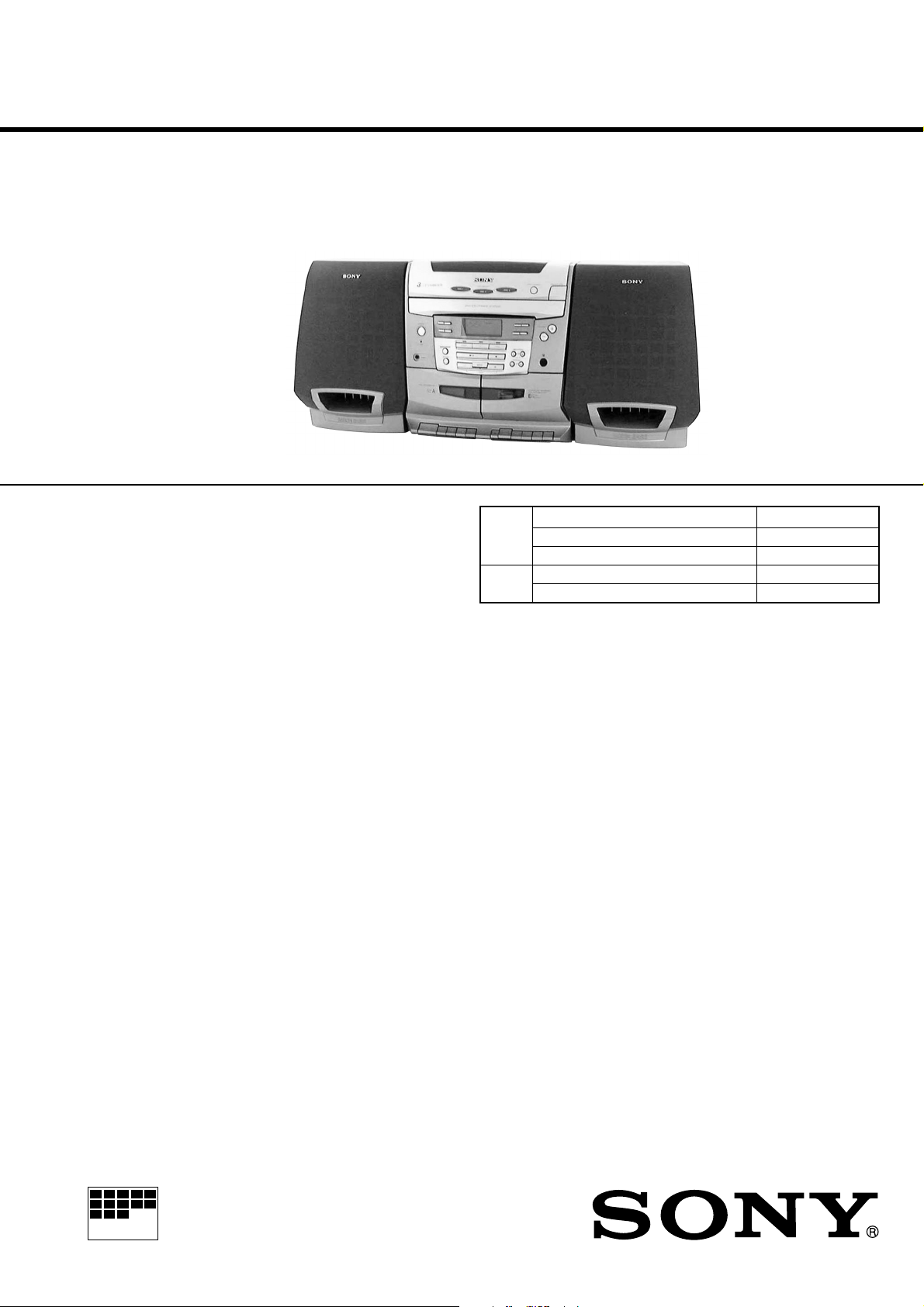
CFD-C1000
MICROFILM
SERVICE MANUAL
Ver 1.2 2000. 10
CD
Section
TC
Section
US Model
Canadian Model
Model Name Using Similar Mechanism NEW
CD Mechanism Type KSM-213CCM
Optical Pick-up Name KSS-213C
Model Name Using Similar Mechanism CFD-ZW150/ZW160
T ape T ransport Mechanism Type MF-ZW150
AUDIO POWER SPECIFICATIONS (US Model)
POWER OUTPUT AND TOTAL
HARMONIC DISTORTION
With 6-ohm loads, both channel driven
from 75 - 15,000 Hz; rated 10 W per
channel-minimum RMS power, with no more
than 1% total harmonic distortion in AC
operation.
Other Specifications
CD player section
System
Compact disc digital audio system
Laser diode properties
Material: GaAlAs
Wave length: 780 nm
Emission duration: Continuous
Laser output: Less than 44.6 µW
(This output is the value measured at a distance of
about 200 mm from the objective lens surface on
the optical pick-up block with 7 mm aperture.)
Spindle speed
200 r/min (rpm) to 500 r/min (rpm) (CLV)
Number of channels
2
Frequency response
20 - 20,000 Hz +1/–2 dB
Wow and flutter
Below measurable limit
SPECIFICATIONS
Radio section
Frequency range
FM: 87.6 - 108 MHz
AM: 530 - 1,710 kHz
Antenna
FM: Telescopic antenna
AM: Loop antenna
Cassette-corder section
Recording system
4-track 2 channel stereo
Fast winding time
Approx. 120 s (sec.) with Sony cassette C-60
Frequency response
TYPE I (normal): 100 - 10,000 Hz
– Continued on next page –
CD RADIO CASSETTE-CORDER
– 1 –

General
Speaker
Full range: 10 cm (4 in.) dia.,
6 ohms, cone type (2)
Outputs
Headphones jack (stereo minijack):
For 16 - 64 ohms impedance headphones
Speaker terminals:
For supplied 6 ohms impedance speaker
Power output (excluding US model)
13 W + 13 W (at 6 ohm, 10 % harmonic
distortion)
Power requirements
For CD radio cassette-corder:
120 V AC, 60 Hz
For remote controller:
3 V DC, 2 size AA (R6) batteries
Power consumption
AC 50 W
Dimensions
Approx. 687 × 297 × 404 mm (w/h/d)
(27 1/8 × 11 3/4 × 16 inches) (incl. projecting parts)
Mass
Approx. 10.5 kg (23 lb. 2 oz.)
Supplied accessories
Remote controller RMT-CC1000A (1)
AM loop antenna (1)
Design and specifications are subject to change without
notice.
CAUTION
Use of controls or adjustments or performance of procedures other than those specified herein may result in hazardous radiation exposure.
Flexible Circuit Board Repairing
• Keep the temperature of the soldering iron around 270˚C during
repairing.
• Do not touch the soldering iron on the same conductor of the
circuit board (within 3 times).
• Be careful not to apply force on the conductor when soldering
or unsoldering.
Notes on Chip Component Replacement
• Never reuse a disconnected chip component.
• Notice that the minus side of a tantalum capacitor may be dam-
aged by heat.
NOTES ON HANDLING THE OPTICAL PICK-UP BLOCK
OR BASE UNIT
The laser diode in the optical pick-up block may suffer electrostatic
breakdown because of the potential difference generated by the
charged electrostatic load, etc. on clothing and the human body.
During repair, pay attention to electrostatic breakdown and also use
the procedure in the printed matter which is included in the repair
parts.
The flexible board is easily damaged and should be handled with
care.
NOTES ON LASER DIODE EMISSION CHECK
The laser beam on this model is concentrated so as to be focused on
the disc reflective surface by the objective lens in the optical pickup block. Therefore, when checking the laser diode emission,
observe from more than 30 cm away from the objective lens.
SAFETY-RELATED COMPONENT WARNING!!
COMPONENTS IDENTIFIED BY MARK ! OR DOTTED LINE
WITH MARK ! ON THE SCHEMATIC DIAGRAMS AND IN
THE PARTS LIST ARE CRITICAL TO SAFE OPERATION.
REPLACE THESE COMPONENTS WITH SONY PARTS WHOSE
P ART NUMBERS APPEAR AS SHOWN IN THIS MANUAL OR
IN SUPPLEMENTS PUBLISHED BY SONY.
ATTENTION AU COMPOSANT AYANT RAPPORT
LES COMPOSANTS IDENTIFIÉS P AR UNE MARQUE ! SUR LES
DIAGRAMMES SCHÉMA TIQUES ET LA LISTE DES PIÈCES SONT
CRITIQUES POUR LA SÉCURITÉ DE FONCTIONNEMENT. NE
REMPLACER CES COMPOSANTS QUE PAR DES PIÈCES SONY
DONT LES NUMÉROS SONT DONNÉS DANS CE MANUEL OU
DANS LES SUPPLÉMENTS PUBLIÉS PAR SONY.
À LA SÉCURITÉ!!
– 2 –
Ver 1.1 2000. 06
SAFETY CHECK-OUT
After correcting the original service problem, perform the following
safety check before releasing the set to the customer:
Check the antenna terminals, metal trim, “metallized” knobs, screws,
and all other exposed metal parts for AC leakage. Check leakage as
described below.
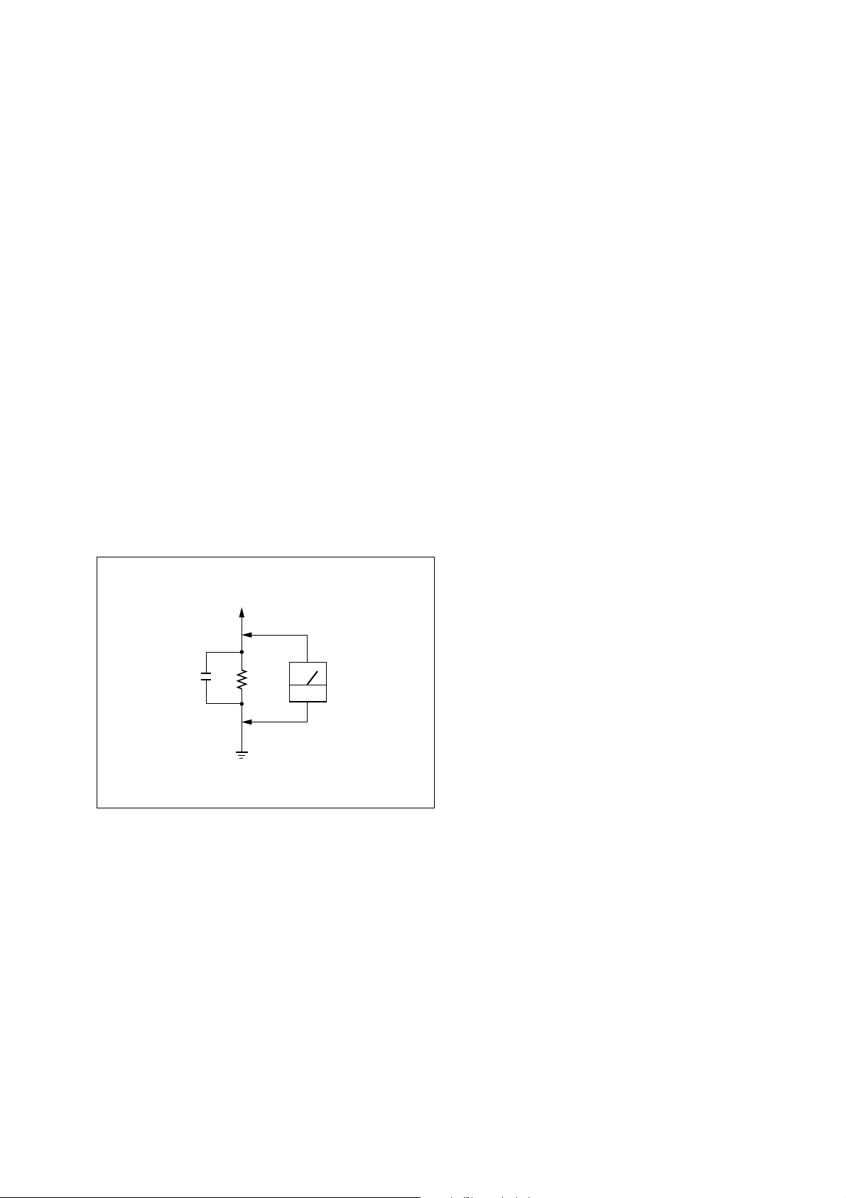
LEAKAGE TEST
The AC leakage from any exposed metal part to earth ground and
from all exposed metal parts to any exposed metal part having a
return to chassis, must not exceed 0.5 mA (500 microamperes).
Leakage current can be measured by any one of three methods.
1. A commercial leakage tester, such as the Simpson 229 or RCA
WT-540A. Follow the manufacturers’ instructions to use these
instruments.
2. A battery-operated AC milliammeter. The Data Precision 245
digital multimeter is suitable for this job.
3. Measuring the voltage drop across a resistor by means of a VOM
or battery-operated AC voltmeter. The “limit” indication is 0.75
V, so analog meters must have an accurate low-voltage scale. The
Simpson 250 and Sanwa SH-63Trd are examples of a passive
VOM that is suitable. Nearly all battery operated digital
multimeters that have a 2V AC range are suitable. (See Fig. A)
To Exposed Metal
Parts on Set
0.15µF
Ω
1.5k
Earth Ground
AC
voltmeter
(0.75V)
TABLE OF CONTENTS
1. GENERAL
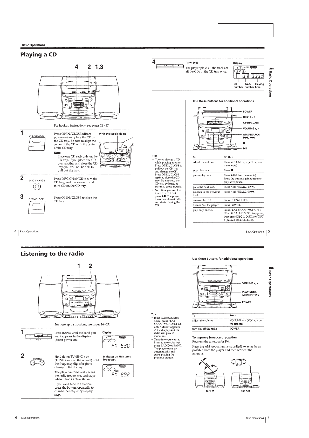
Playing a CD ........................................................................... 4
Listening to the radio ............................................................... 4
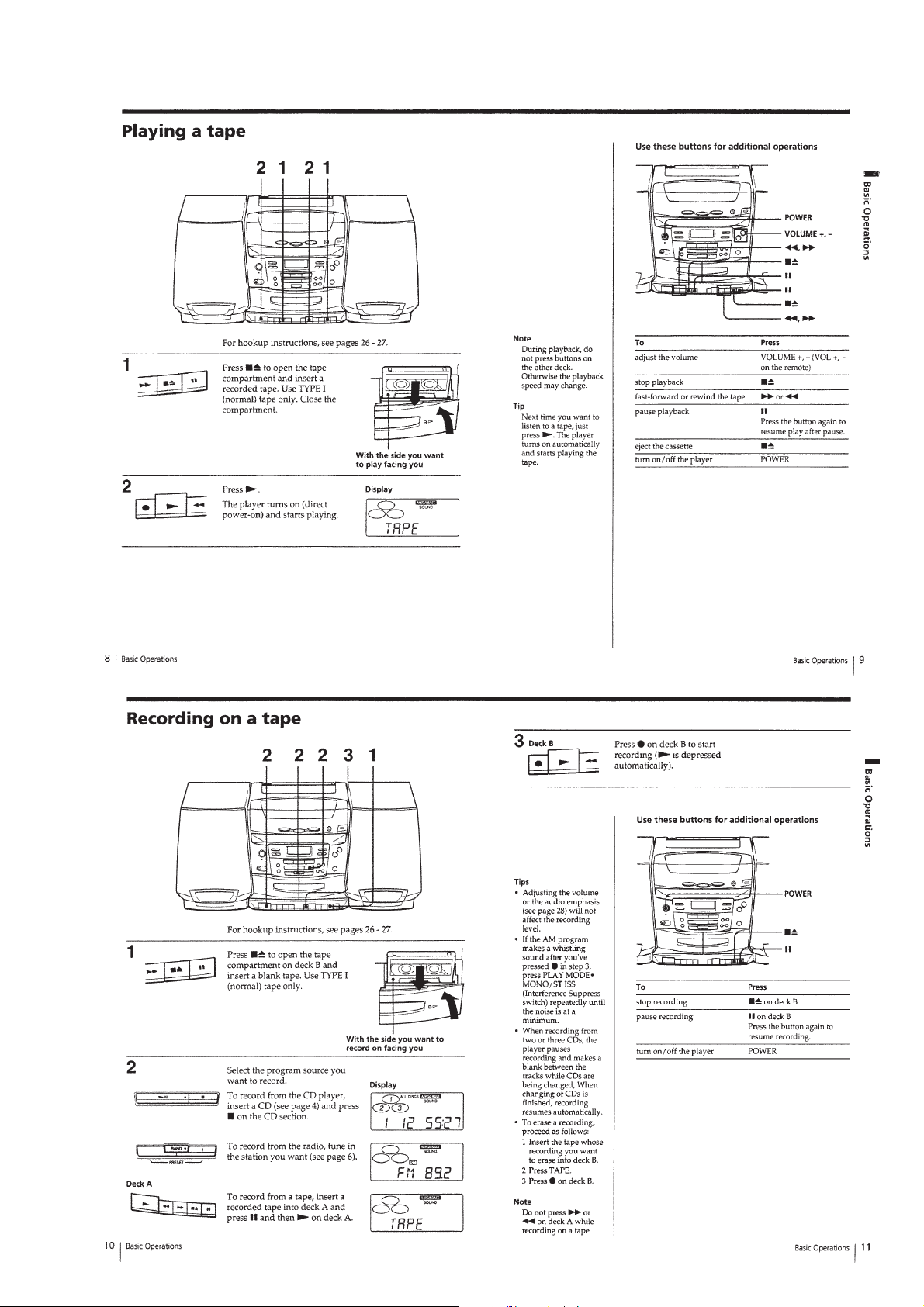
Playing a tape .......................................................................... 5
Recording on a tape ................................................................. 5
2. DISASSEMBLY
2-1. “Top Assy, Cabinet”, “Changer Assy, CD”.........................6
2-2. Rear Assy, Cabinet .............................................................. 6
2-3. Power Board........................................................................7
2-4. Mechanism Deck Block ...................................................... 7
2-5. Main Board ......................................................................... 8
2-6. LCD Board .......................................................................... 8
2-7. CD Lamp Board and Disc Board and Display Board .........9
2-8. Base, Changer ..................................................................... 9
2-9. Optical Pick-up ................................................................. 10
3. MECHANICAL ADJUSTMENTS............................... 11
4. ELECTRICAL ADJUSTMENTS
Tape Section .......................................................................... 11
Tuner Section.........................................................................13
CD Section ............................................................................ 14
5. DIAGRAMS
5-1. IC Pin Description.............................................................15
5-2. Circuit Boards Location .................................................... 16
5-3. Block Diagram –CD Section–...........................................17
5-4. Block Diagram –Main Section–........................................19
5-5. Printed Wiring Boards –Key Section– .............................. 21
5-6. Schematic Diagram –Key Section–...................................23
5-7. Printed Wiring Board –Audio Section– ............................ 25
5-8. Schematic Diagram –Audio Section– ............................... 27
5-9. Printed Wiring Boards –CD Section– ............................... 29
5-10. Schematic Diagram –CD Section–.................................... 31
5-11. Printed Wiring Boards –Control Section–......................... 33
5-12. Schematic Diagram –Control Section– ............................. 35
5-13. Printed Wiring Boards –Power Supply Section– .............. 37
5-14. Schematic Diagram –Power Supply Section–................... 39
5-15. Schematic Diagram –Tuner Section–................................ 41
Fig. A. Using an AC voltmeter to check AC leakage.
6. EXPLODED VIEWS
6-1. Rear Cabinet Section.........................................................48
6-2. Front Cabinet Section-1 ....................................................49
6-3. Front Cabinet Section-2 ....................................................50
6-4. CD Changer Section-1 ......................................................51
6-5. CD Changer Section-2 ......................................................52
6-6. Tape Mechanism Deck Section-1 ...................................... 53
6-7. Tape Mechanism Deck Section-2 ...................................... 54
6-8. Tape Mechanism Deck Section-3 ...................................... 55
6-9. Optical Pick-up Section .................................................... 56
6-10. Speaker Section ................................................................. 57
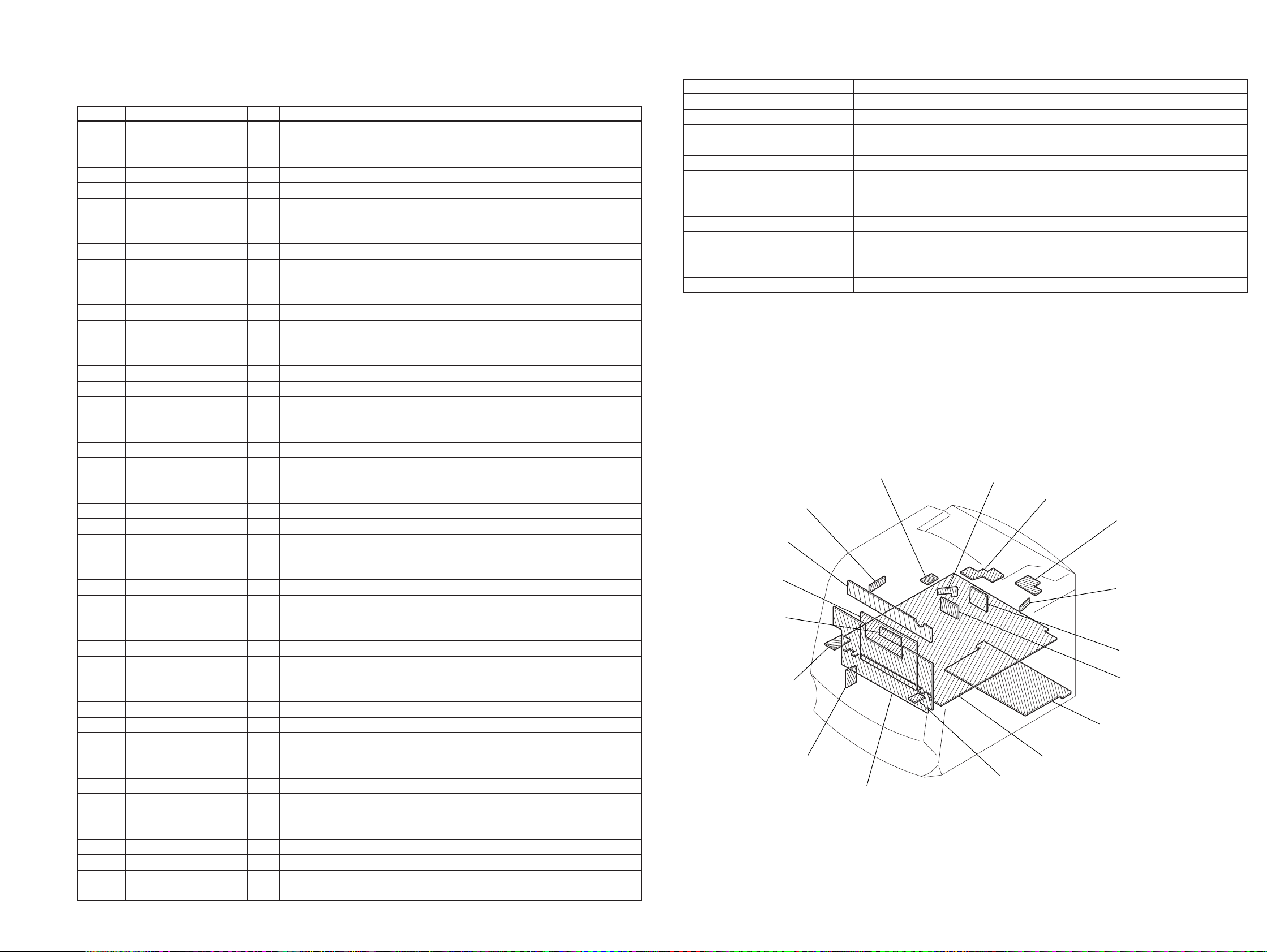
7. ELECTRICAL PARTS LIST......................................... 58
– 3 –
SECTION 1
GENERAL
This section is extracted
from instruction manual.
– 4 –
– 5 –
play
D
8
t
Ver 1.1 2000. 06
SECTION 2
DISASSEMBLY
• The equipment can be removed using the following procedure.
Set “Top Assy, Cabinet”,
“Changer Assy, CD”
Note : Follow the disassembly procedure in the numerical order given.
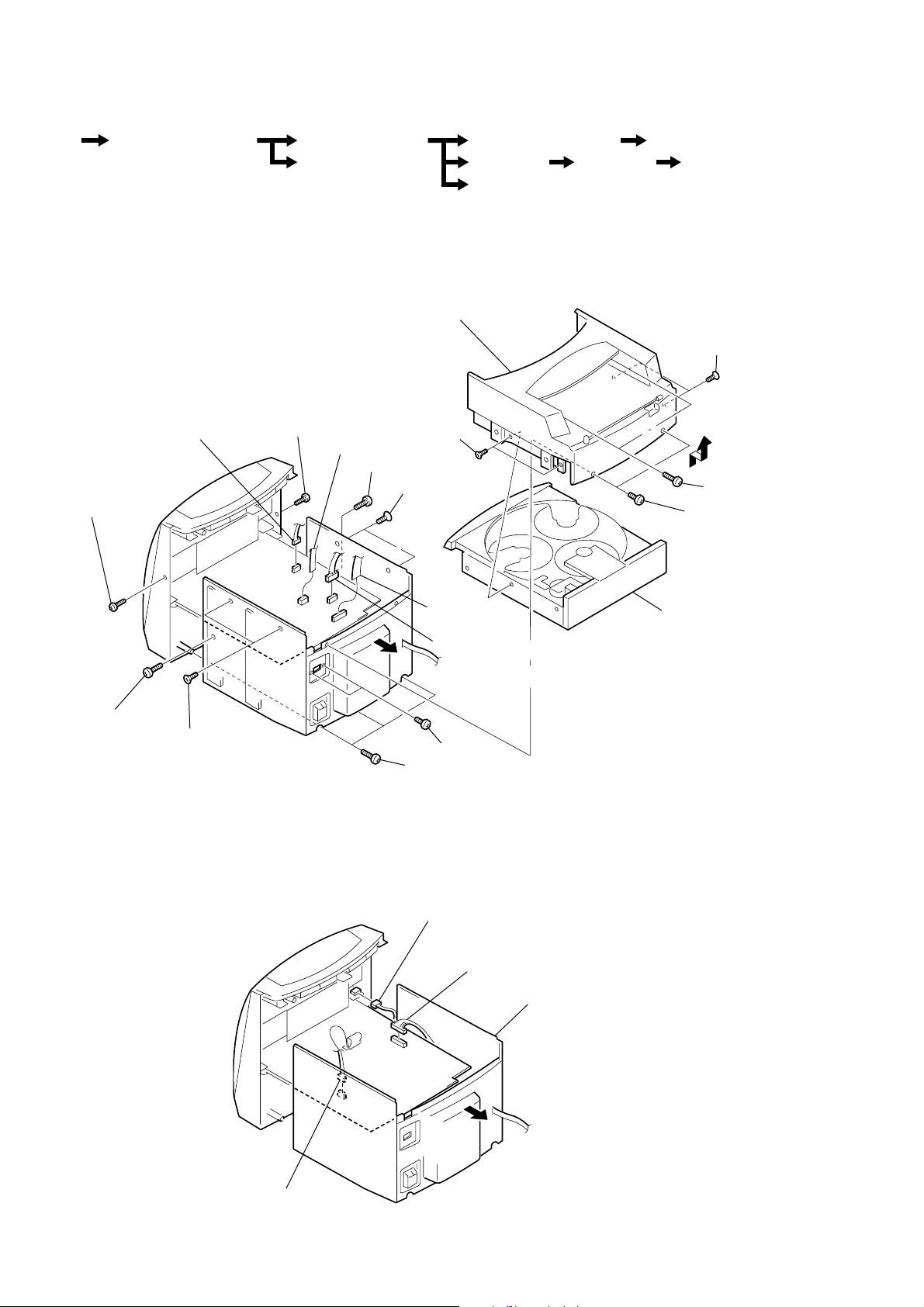
2-1. ‘‘TOP ASSY, CABINET’’, ‘‘CHANGER ASSY, CD’’
Rear Assy, Cabinet
Base, Changer
w; top assy, cabinet
Mechanism Deck Block Optical Pick-up
Main Board LCD Board
Power Board
CD Lamp Board
and Disc Board
and Dis
qk KTP 3x
Board
qh CN707
3 BTP 3x14
4 BTP 3x8
5 KTP 3x8
2-2. REAR ASSY, CABINET
6 BTP 3x14
qg CN706
qj KTP 3x8
7 BTP 3x8
8 KTP 3x8
qa
9 BTP 3x10
qd CN702
qf CN701
0 BTP 3x8
qs
1 BTP 3x14
2 BTP 3x8
ql changer assy, C
3 CN313
1 CN308
2 CN314
5 rear assy, cabine
4
– 6 –
8
Ver 1.1 2000. 06
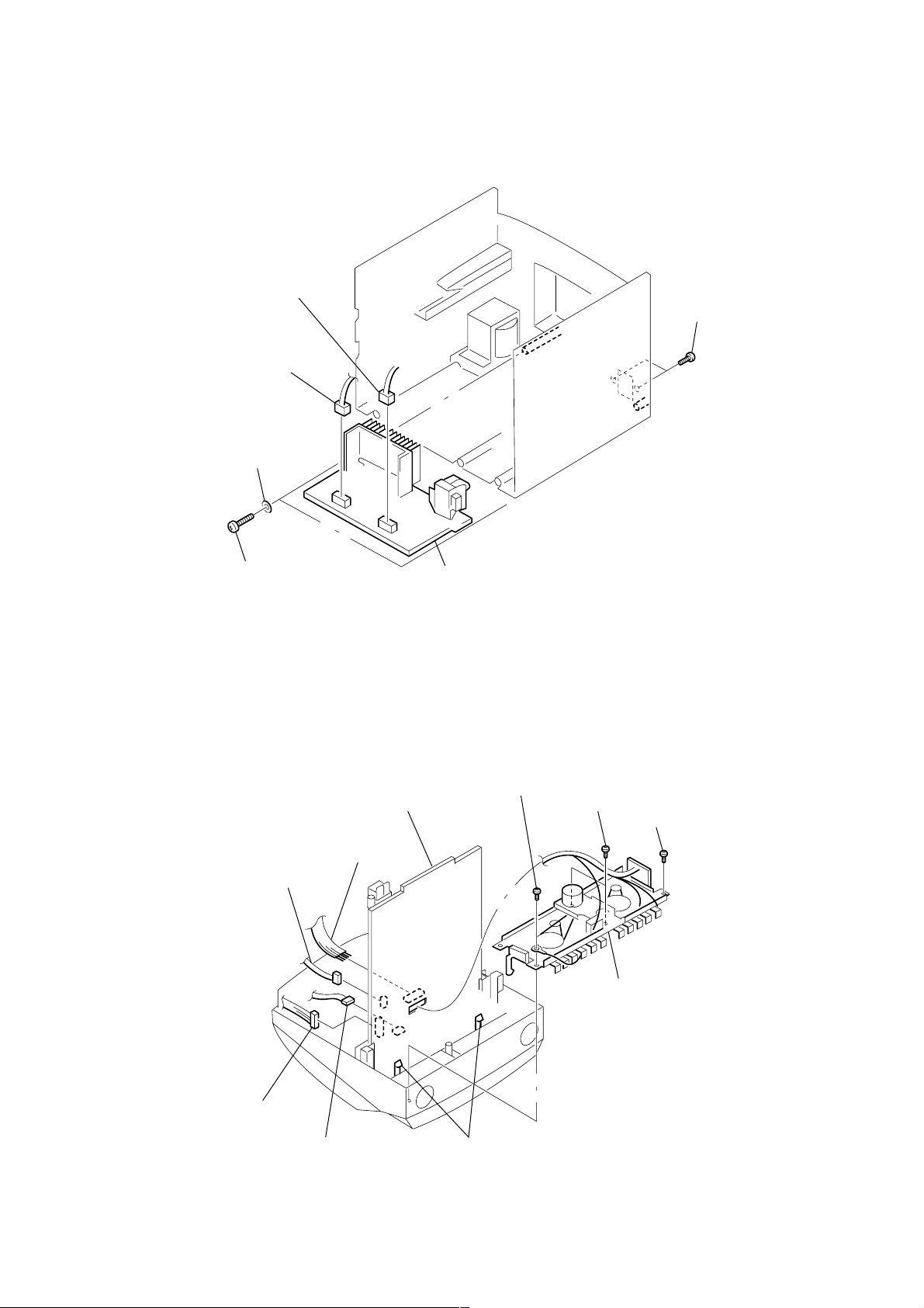
2-3. POWER BOARD
5 CN307
3 screws BTP 3x
4 CN306
2 washers
1 screws BTP 3x10
2-4. MECHANISM DECK BLOCK
2 CN301
MAIN board
1 CN305
6 POWER board
7 screw BTP 3x10
6 screws BTP 3x10
5 screw BTP 3x10
9 mechanism deck block
4 CN302
3 CN303
8 claws
– 7 –
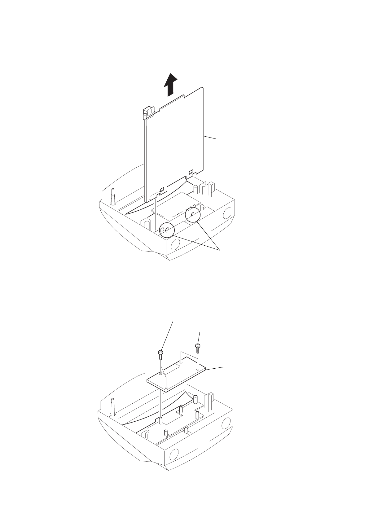
2-5. MAIN BOARD
d
2
3
MAIN board
2-6. LCD BOARD
1
claws
2
screws BTP 3x8
1
screws BTP 3x8
3
LCD boar
– 8 –
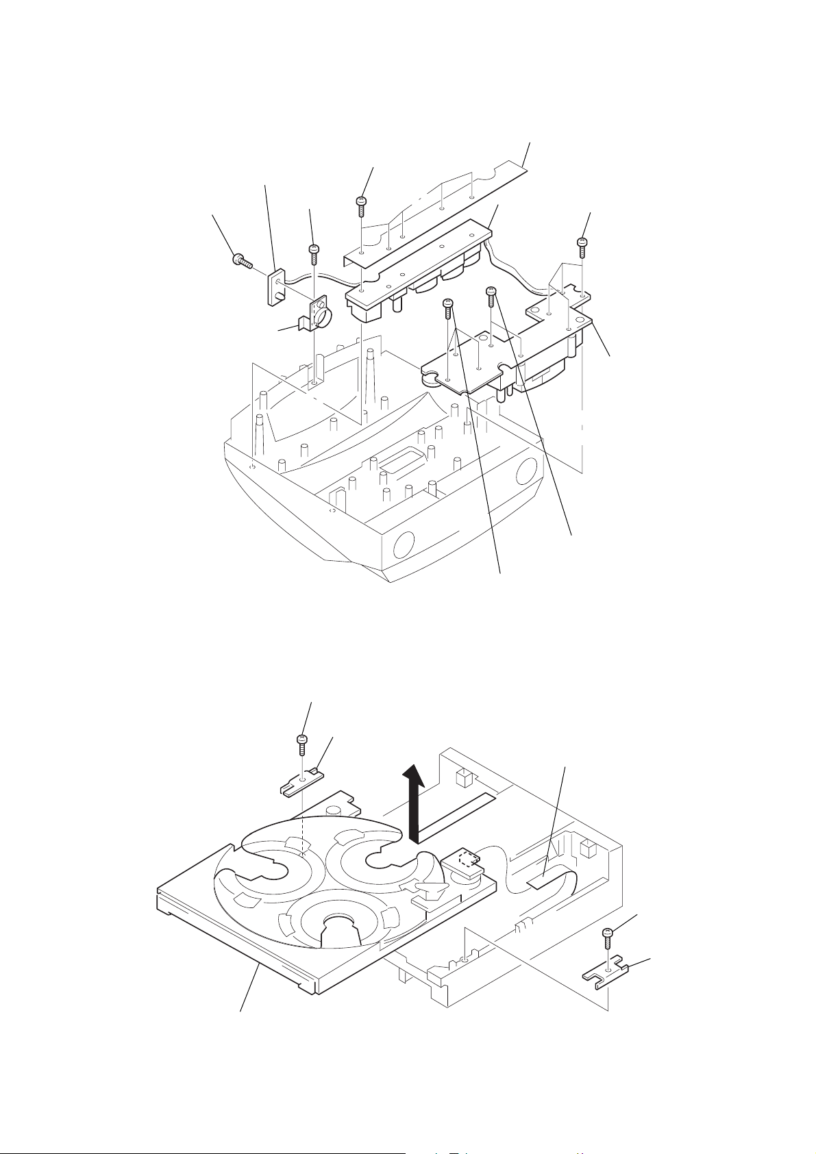
2-7. CD LAMP BOARD AND DISC BOARD AND DISPLAY BOARD
d
8
5
screws BTP 3x8
4
CD LAMP board
3
screw
2
holder, CD lamp
1
screw
7
6
cover, disc board
DISC board
8
screws BTP 3x8
!¡
DISPLAY boar
2-8. BASE, CHANGER
1
screw P 2.6x8
2
guide, rail
6
!º
screws BTP 3x8
9
screws BTP 3x8
5
CN6
3
screw P 2.6x
base, changer
– 9 –
4
guide, rail
Ver 1.1 2000. 06
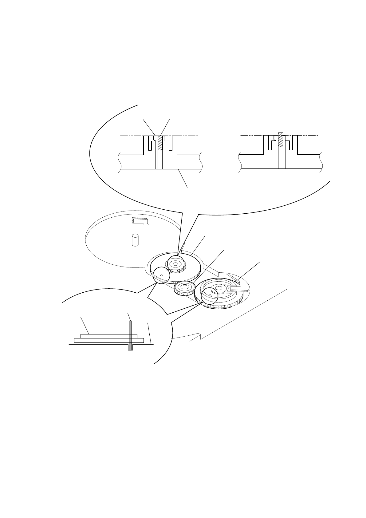
• NOTE FOR INSTALLATION OF THE “BASE, CHANGER”
It is important for the CD changer mechanism to ensure a proper
alignment between the “gear, tray” and the “gear, tray rock”.
2 There are two types of “gear, tray” available: screw fastening type and rubber fit type.
For the rubber fit type of “gear, tray” , fit the rubber in the boss on the “gear, tray” .
Do not allow the rubber to project. Take care not to damage the claw.
claw
rubber
OK NG
gear, tray
gear, tray
gear (C), relay
gear, tray rock
gear
1 Pass a pin of 1.5 mm diameter through the holes in the “gear , tray ” and the “gear, tray rock”
and align these holes with the hole in the “base, changer”.
pin
base, changer
– 11 –
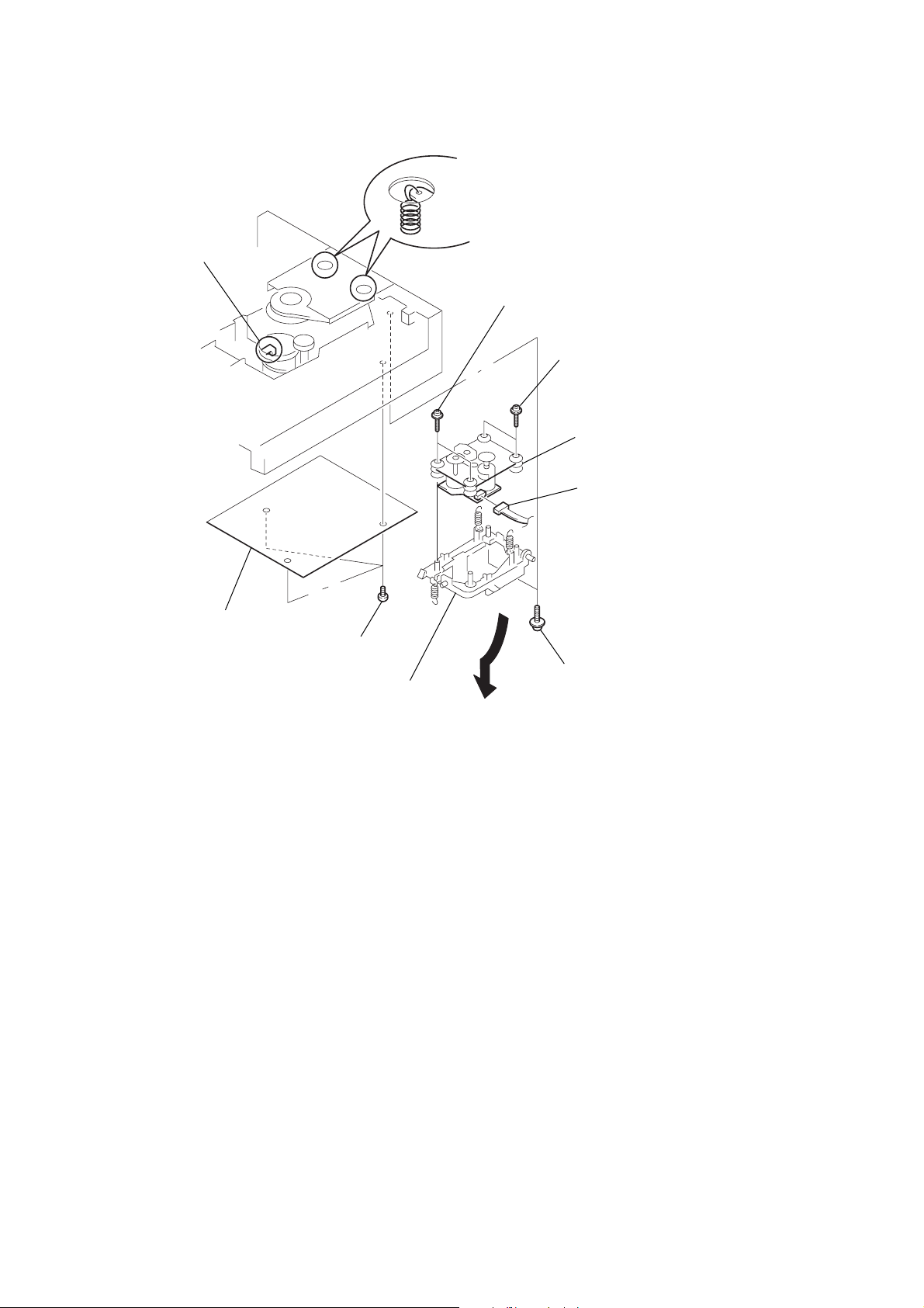
2-9. OPTICAL PICK-UP
)
4
Take off the spring.
Take off the spring.
3
9
screws tapping, (M2.6x20)
0
screws tapping, (M2.6x20
!¡
optical pick-up
5
connector
2
plate, fiber
1
screws
8
mechanism assy, CD
7
6
screws PTPWH 3x8
– 10 –
SECTION 3
y
MECHANICAL ADJUSTMENTS
SECTION 4
ELECTRICAL ADJUSTMENTS
PRECAUTION
1. Clean the following parts with a denatured alcohol-moistened
swab :
record/playback head capstan idlers
playback head pinch roller
erase head rubber belts
2. Demagnetize the record/playback head with a head demagne-
tizer. (Do not bring the head demagnetizer close to the erase
head.)
3. Do not use a magnetized screwdriver for the adjustments.
4. After the adjustments, apply suitable locking compound to the
parts adjusted.
5. The adjustments should be performed with the rated power
supply voltage unless otherwise noted.
Torque Measurement DECK A DECK B
Mode Torque meter Meter reading
Forward CQ-102C
Forward
back tension (0.03 to 0.07 oz • inch)
Fast Forward
and CQ-201B
Rewind
CQ-102C
22.5 to 55 g • cm
(0.31 to 0.76 oz • inch)
2 to 5 g • cm
60 to 120 g • cm
(0.83 to 1.67 oz • inch)
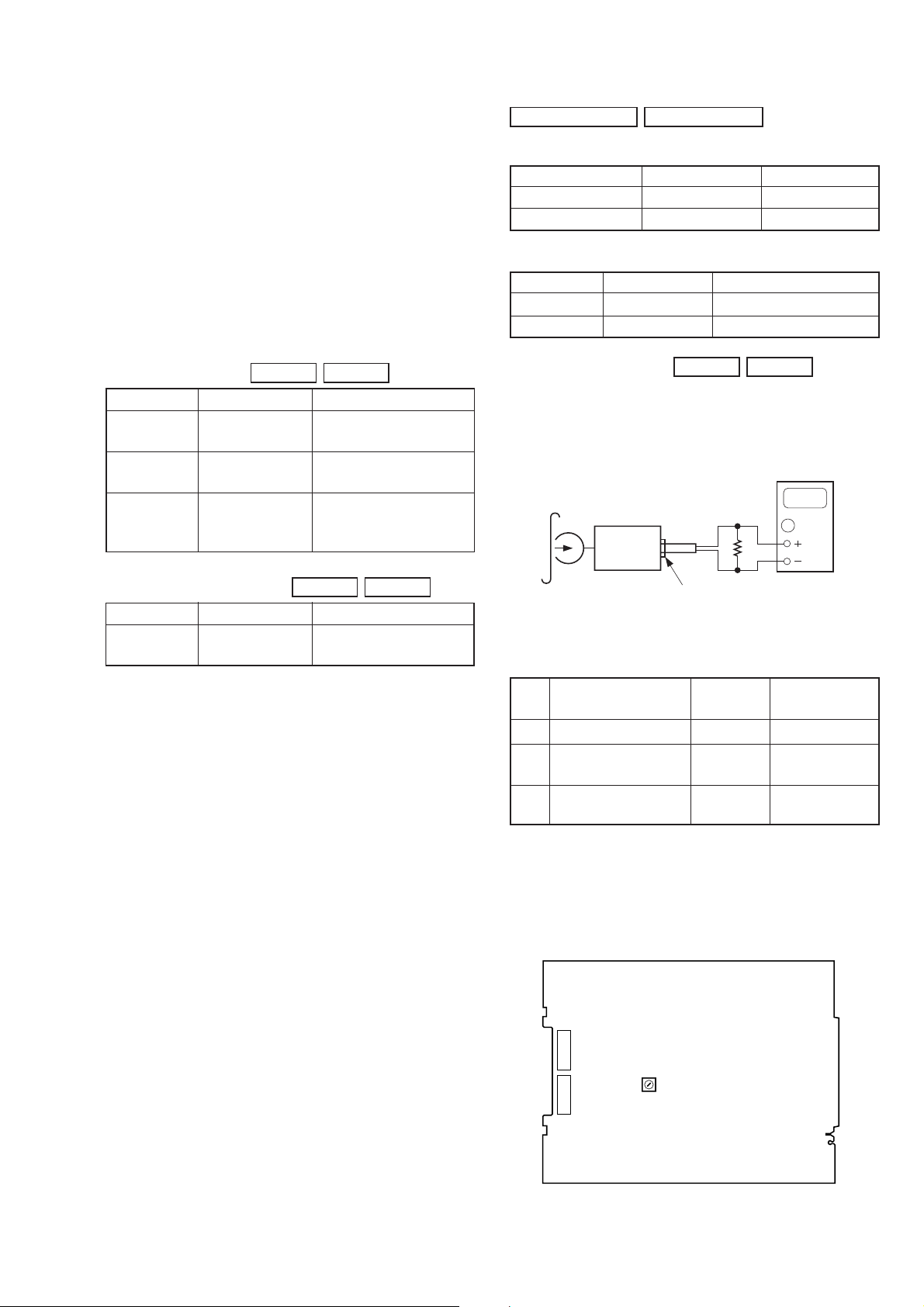
TAPE SECTION 0 dB = 0.775 V
Standard Output Level
Output terminal SP OUT PHONES OUT
load impedance 6 Ω 32 Ω
output signal level 0.775 V (0 dB) 0.25 V (–10 dB)
Test T ape
Tape Signal Used for
WS-48A 3 kHz, 0 dB tape speed adjustment
P-4-A063 6.3 kHz, –10 dB head azimuth adjustment
Tape Speed Adjustment DECK A DECK B
Procedure:
• Perform normal speed adjustment before high speed check.
Mode: playback (deck A)
record (deck B)
test tape
WS-48A
(3 kHz, 0 dB)
set
digital frequenc
counter
Ω
32
0000
Tape Tension Measurement DECK A DECK B
Mode Tension meter Meter reading
Forward CQ-403A
more than 150 g
(more than 5.29 oz)
PHONES jack (JK302)
Adjust SFR301 so that the value on the digital frequency counter is
3 kHz.
Specification Value:
Deck
A Normal (playback) SFR301 2,985 to 3,015 Hz
A HI-SPEED DUBBING
B HI-SPEED DUBBING
Frequency difference between the beginning and the end of the
tape should be within ± 1.5% (both Normal and Hi-speed).
Adjustment Location:
– main board (component side) –
Tape Adjustment Frequency
speed point counter
(playback)
(record)
(confirmation)
——— ———
5,700 to 6,500 Hz
CN801
SFR301
CN802
TAPE
SPEED
ADJUSTMENT
– 11 –
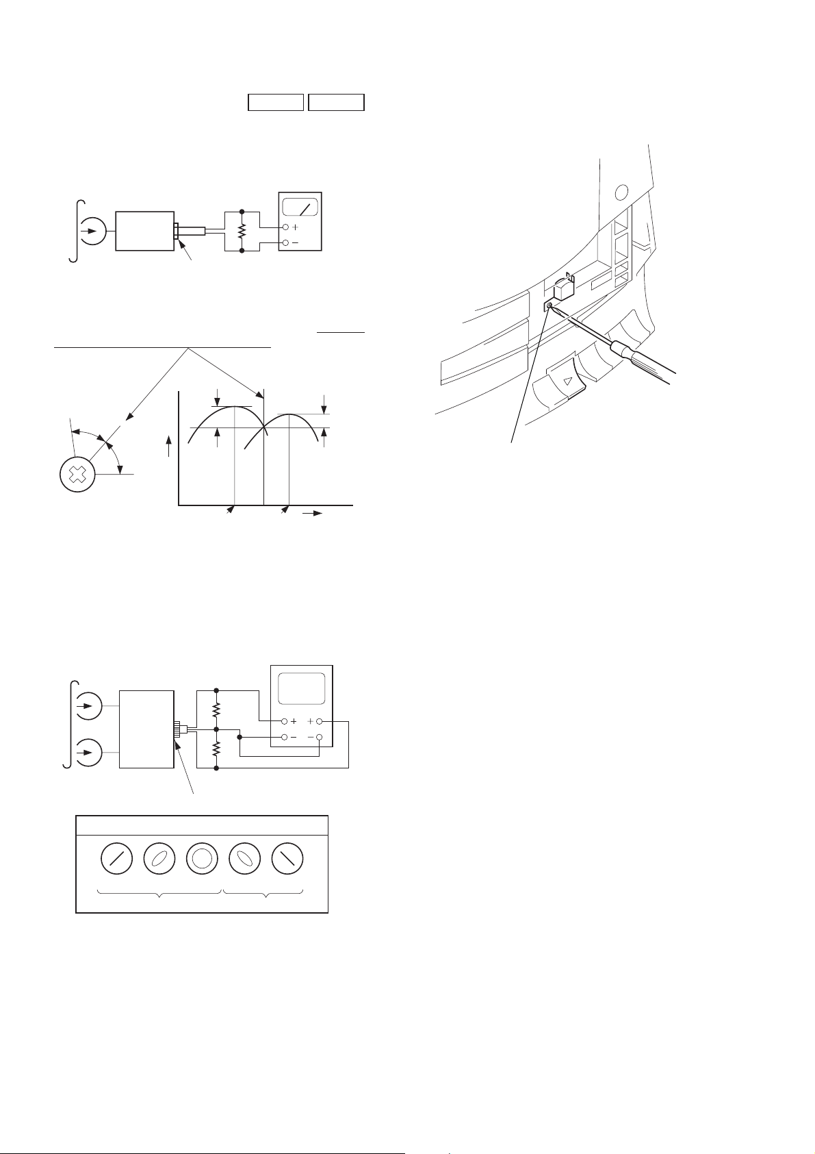
n
REC/PB Head Azimuth Adjustment DECK A DECK B
Procedure:
1. Mode: playback
test tape
P-4-A063
(6.3 kHz, –10 dB) level meter
32
Ω
set
PHONES jack (JK302)
2. Turn the adjustment screw for the maximum output levels. If
these levels do not match. Turn the adjustment screw until both
of output levels match together within 1 dB.
Adjustment Location: playback head (deck A)
record/playback head (deck B)
L-CH
peak
screw
position
3. Phase Check
Mode: playback
test tape
P-4-A063
(6.3 kHz, –10 dB)
R-CH
peak
Output
level
L-CH
set
R-CH
within
1 dB
L-CH
peak
L-CH
32
32
R-CH
PHONES jack (JK302)
R-CH
peak
Ω
Ω
withi
1 dB
adjustment screw
angle
osilloscope
VH
Screen pattern
in phase 45˚ 90˚ 135˚ 180˚
good wrong
Note: Finish the screw adjustment with a turn in the clockwise
direction.
After the adjustment, lock the adjustment screw.
– 12 –
TUNER SECTION 0 dB = 1 µV
)
• FM Section
Setting:
BAND switch: FM
FM RF signal
generator
antenna terminal
0.01
µ
F
set
22.5 kHz frequency
deviation by 1 kHz signal
Output level : as low as possible
• AM Section
Setting:
BAND switch: AM
AM RF signal
generator
Put the lead-wire
antenna close to
the AM loop
antenna.
30% amplitude
modulation by 400 Hz signal
Output level : as low as possible
• Connecting Level Meter (FM and AM)
level meter
(range: 0.5-5 V ac
Ω
32
set
FM FREQUENCY COVERAGE
CHECK
Frequency Display 87.5 MHz 108 MHz
Reading on Digital voltmeter 2.0 ± 0.2 V 7.3 ± 0.1 V
Adjustment Part <confirmation> <confirmation>
FM TRACKING CHECK
Adjust for a maximum reading on level meter.
<confirmation> <confirmation>
87.5 MHz 108 MHz
AM IF ADJUSTMENT
Adjust for a maximum reading on level meter.
T2
450 kHz
AM FREQUENCY COVERAGE
ADJUSTMENT
Frequency Display 530 kHz 1,710 kHz
Reading on Digital voltmeter 1.2 ± 0.1 V 7.5 ± 0.2 V
Adjustment Part L5 <confirmation>
AM TRACKING ADJUSTMENT
Adjust for a maximum reading on level meter.
L4 TC2
620 kHz 1,400 kHz
Adjustment Location: See page 14.
PHONES jack (JK302)
• Connecting Digital Voltmeter (FM and AM)
digital
voltmeter
100 k
TP1 (VT)
Ω
• Repeat the procedures in each adjustment several times, and the
frequency coverage and tracking adjustments should be finally
done by the trimmer capacitors.
– 13 –
R
Adjustment Location: main board
– main board (component side) –
IC2
CD SECTION
CD section adjustments are done automatically in this set.
In case of operation check, confirm that focus bias.
IC3
FE1
TP1
(VT)
T2
AM
IF
ADJUSTMENT
TC2
AM
TRACKING
L4
ADJUSTMENT
L5
AM
FREQUENCY
COVERAGE
ADJUSTMENT
FOCUS BIAS CHECK
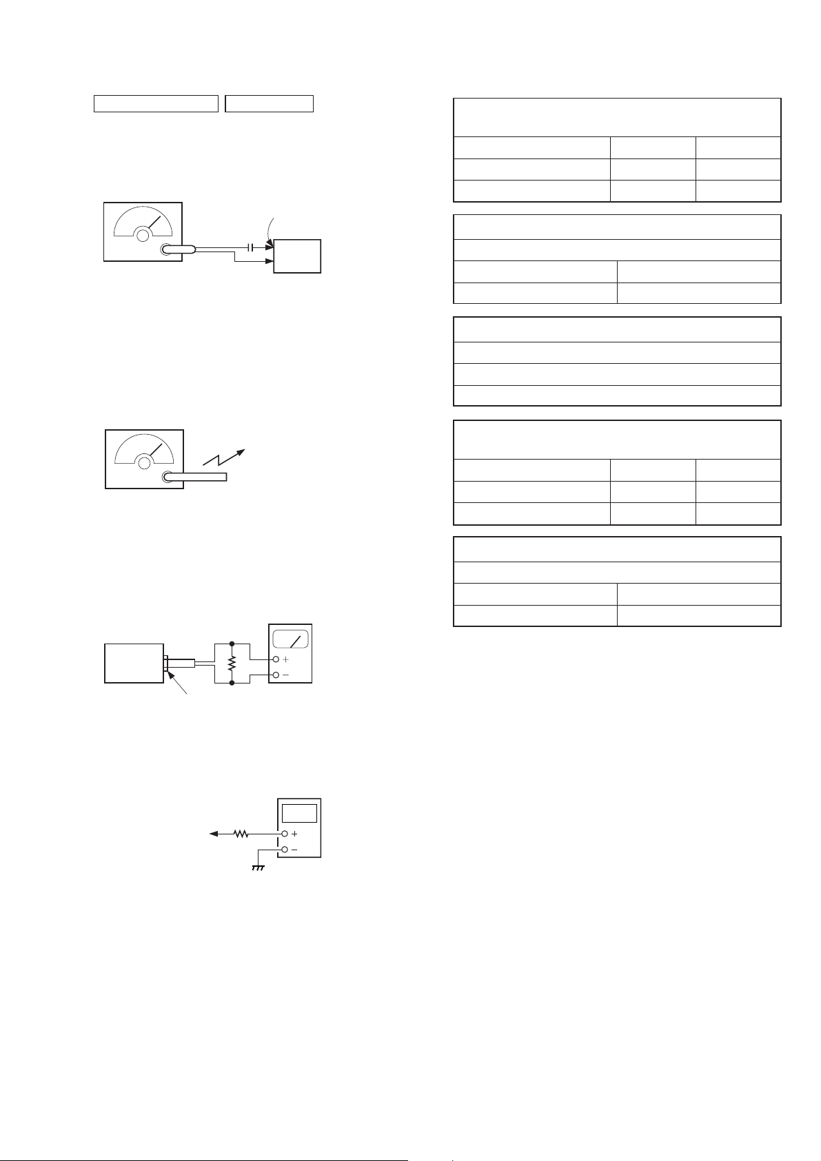
1. Connect the oscilloscope between IC701 pin #£ (TP RFO) and
GND on Main board.
2. Insert the disc (YEDS-18). (Part No. : 3-702-101-01)
3. Press the ^ button.
4. Confirm that the oscilloscope waveform is as shown in the
figure below. (eye pattern)
A good eye pattern means that the diamond shape ( ) in the
center of the waveform can be clearly distinguished.
• RF signal reference waveform (eye pattern)
VOLT/DIV : 200 mV (10 : 1 probe in use)
TIME/DIV : 500 nS
RF level :
±
0.5 Vp-p
1.3
When observing the eye pattern, set the oscilloscope for AC range
and raise vertical sensitivity.
π
Test Point:
TP (RFO)
– main board (conductor side) –
TP (RFO)
C718A
C706
R701
C701
R707
C703
C707
R713
R718
C704
BCE
39
40
S301
RESET
Q701
R705
R706
R704
C736
R716
R714
R717
R715
C705
27
IC701
55
R721
C702
R778
C731
26
56
C757
R736
R777
R728
C733
R738
14
1
C752
726
– 14 –
SECTION 5
MOTOR board
AC board
SWITCH (A) board
SWITCH (B) board
SWITCH (C) board
SWITCH (D) board
POWER board
MAIN board
REMOCON board
DISPLAY board
MD board
HEADPHONE board
LCD board
DISC board
LAMP board
CD MOTOR board
CD LAMP board
DIAGRAMS
5-1. IC PIN DESCRIPTION
• IC801 CXP83232A-013Q (SYSTEM CONTROL)
Pin No. Pin Name I/O Pin Description
1 AC CHK I AC power detect (L: AC power on)
2 SCOR I CD SCOR input
3 RMC I Sircs receiver input
4 SCL O Volume serial chip enable output
5 NC — Not used
6 SENS2 I CD SENSE2 input
7 XLAT O CD serial latch output
8 CLOK O CD serial clock output
9 NC — Not used
10 DATA O CD serial data output
11 SQCK O CD Sub-Q read clock output
12 SQSO I CD Sub-Q data input
13 SENS I CD SENSE1 input
14 CLOK O CD motor clock output
15 CE OUT O Tuner PLL chip enable output
16 DO IN I Tuner PLL data input
17 DATA OUT O CD motor data output
18 STB OUT O CD motor standby signal output
19 NC — Not used
20 REC BEAT CONTROL O ISS control signal output (H: 1, L: 2)
21 MEGA BASS O Mega bass control signal output (L: Mega bass on)
22 SDA O Volume serial data output
23 LED VDD O LED power control signal output (L: LED power on)
24 TURN TABLE SW IN I Turn table switch input
25 DISC NO. SW IN I Disc No. switch input
26 TRAY OPEN SW IN I CD tray open switch input
27 TRAY CLOSE SW IN I CD tray close switch input
28 TRAVERSE UP SW IN I CD mechanism up switch input
29 TRAVERSE DOWN SW IN I CD mechanism down switch input
30 – 33 KEY1 – 4 I key input
34 REC I Tape record signal input
35 MODE SW O Mode set pin
36 SFC O Shift clock on/off output
37 FM STEREO IN I Tuner stereo signal input
38 RESET I System reset input (L: Reset)
39 EXTAL1 I Oscillation input (4.19 MHz)
40 XTAL1 O Oscillation output (4.19 MHz)
41 VSS — GND
42 NC — Not used
43 VSS — GND
44 AVREF — Reference voltage input
45 AVSS — GND
46 VL — LCD drive bias VDD
47 – 49 VLC3 – 1 I LCD drive bias 3 – 1
50 – 53 COM0 – 3 O LCD drive common output
54 – 80 SEG0 – 26 O LCD drive segment output
81 NC — Not used
82 POWER SW OUT O Power AMP control signal output (H: Power amp on)
83 SYSTEM MUTE O Audio signal mute output (H: Mute)
84 TUNER MUTE O Tuner signal mute output (H: Mute)
85 CD MUTE O CD signal mute output (H: Mute)
Pin No. Pin Name I/O Pin Description
86 CD LED O LED (CD) drive signal/CD function signal output (H: CD)
87 TAPE LED O LED (TAPE) drive signal output (H: LED on)
88 RADIO LED O LED (RADIO) drive signal/Radio function signal output (H: Radio)
89 VDD — Power supply pin (+5 V)
90 VDD NC — Power supply pin (+5 V)
91 VSS — GND
92 TX O Oscillation output (32.768 kHz)
93 TEX I Oscillation input (32.768 kHz)
94 – 96 LED1 – 3 O LED (DISC1 – 3) drive signal output (H: LED on)
97 LCD BACK LIGHT O LCD back light control signal output (H: Lamp on)
98 MOTOR CONT OUT O Motor control signal output (H: Motor on)
99 TC A I Tape play switch input (L: Deck A on)
100 TC B I Tape play switch input (L: Deck B on)
5-2. CIRCUIT BOARDS LOCATION
– 15 – – 16 –
CFD-C1000
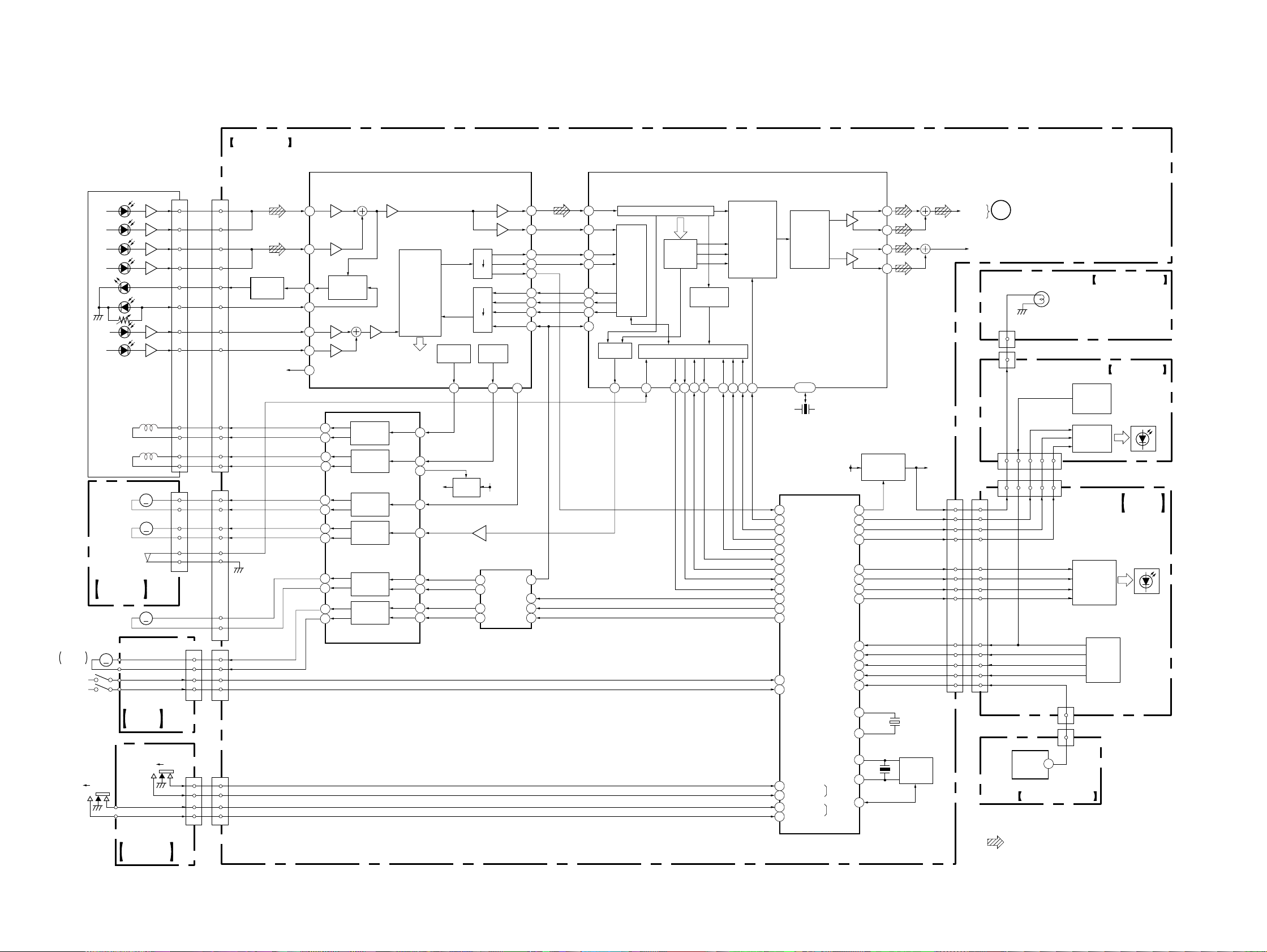
5-3. BLOCK DIAGRAM — CD SECTION —
MAIN BOARD (1/2)
M704
TABLE
ROTATE
S04
(MOVE)
S03
(DISC COUNTER)
S02
(OPEN/CLOSE)
OPEN CLOSE
A
C
B
D
LD
PD
E
F
OPTICAL PICK-UP
(KSS-213C)
TRACKING
COIL
FOCUS
COIL
M702
(SLED)
M701
(SPINDLE)
S701
(LIMIT)
CD MOTOR
BOARD
M703
(TRAY)
M
SWITCH (D)
BOARD
04
BLOCK
M
M
M
MOTOR
BOARD
(CD UP/DOWN)
DOWN UP
10
12
14
15
13
16
CNP707
CN6 CN706
S01
CN5 CN707
RF AMP, SERVO CONTROL
CN701
5
7
6
4
3
8
4
3
5
6
1
2
5
7
6
4
10
12
14
15
13
16
4
5
2
1
1
2
5
3
3
8
CN702
4
3
5
6
1
2
8
7
4
5
2
1
1
2
5
3
LD DRIVE
Q701
VREF
PD1
38
PD2
39
LASER
LD
DIODE
36
CONTROL
PD
37
E
42
F
41
VC
51
TRACKING
3
4
2
1
18
17
20
19
30
31
14
13
FOCUS/TRACKING COIL DRIVE,
MOTOR DRIVE
FE AMP
COIL
DRIVE
FOCUS
COIL
DRIVE
SLED
MOTOR
DRIVE
SPINDLE
MOTOR
DRIVE
TRAY
MOTOR
DRIVE
TT
MOTOR
DRIVE
IC703
RF AMP
IC701
SERIAL/
PARALLEL
CONVERTER
DECODER
COMMAND
TRACKING
PHASE
5
6
10
+5V +7.5V
22
21
29
28
13
12
TAO
13
+5V REG
Q703
15
RF O
33 35
FOK
27
C. OUT
IIL
TTL
TTL
IIL
FOCUS
PHASE
FEO
6 16 7
IC705
TRAY+
13
TRAY–
12
TT+
7
TT–
14
MOTOR CONTROL
SENS1
SENS2
IC704
DATA
XLT
CLK
XRST
XRST
CLOCK
DATAI
STB
24
25
26
22
21
20
23
SLO
6
3
2
1
RF
FOK
18
CNIN
11
SEIN
10
DATO
12
XLTO
13
CLKO
14
79
XRST
DIGITAL
CLV
MDP
21
EFM DEMODULATOR
SERVO
AUT
SEQ.
SPOA
15
INTERFACE
DIGITAL SIGNAL PROCESSOR
D/A
SUB CODE
PROCESSOR
CPU INTERFACE
SENS
SQSO
SQCK
SCOR
574
6
5
DATA
IC702
SERIAL
INTERFACE
XLAT
CLOK
8 9 62
SYSM
DIGITAL
FILTER
D/A
CONVERTER
XTAI
70•71
XTL1
16.9344MHz
SYSTEM CONTROL
IC801 (1/2)
SENS2
6
CD MUTE
85
CLOK
8
7
XLAT
10
DATA
SCOR
2
SQCK
11
12
SQSO
13
SENS
CLOK
14
17
DATA OUT
STB OUT
18
TURN TABLE SW
24
IN
25
DISC ON SW IN
UP SW IN
28
DOWN SW IN
29
OPEN SW IN
26
CLOSE SW IN
27
&
XTAO
BACK LIGHT
POWER SW
RADIO LED
PWM
AMP
PWM
AMP
+9.5V
LCD
LED1
LED2
LED3
OUT
CD LED
TAPE LED
KEY1
KEY2
KEY3
KEY4
REM
TXE
EXTAL1
XTAL1
TRAVERSE
SFC
TRAY
TX
AOUT1
LOUT1
AOUT2
LOUT2
LAMP POWER
CONTROL
Q809,810
97
94
95
96
82
86
87
88
30
31
32
33
3
92
93
39
40
X801
4.19MHz
36
65
67
76
74
X802
32.768kHz
OSC
CONTROL
Q801,802
+B
LAMP
CN804
CD L-CH
17
13
14
15
16
7
5
6
4
3
2
1
12
R-CH
CN803A
17
13
14
15
16
7
5
6
4
3
2
1
12
CN804
MAIN
1
SECTION
CN806
2
2
CN806
RM801
REMOCON BOARD
CD LAMP BOARD
TURN TABLE
LP804
LAMP
LP804
DISC BOARD
KEY
MATRIX
S826-830
LED
DRIVE
Q806-808
43278
432278
CN803B
DISPLAY
BOARD
LED
DRIVE
Q803-805,809
KEY
MATRIX
S801-824
CN805
2
CN805
2
RO
• Signal path
: CD
• R-ch : same as L-ch.
– 17 – – 18 –
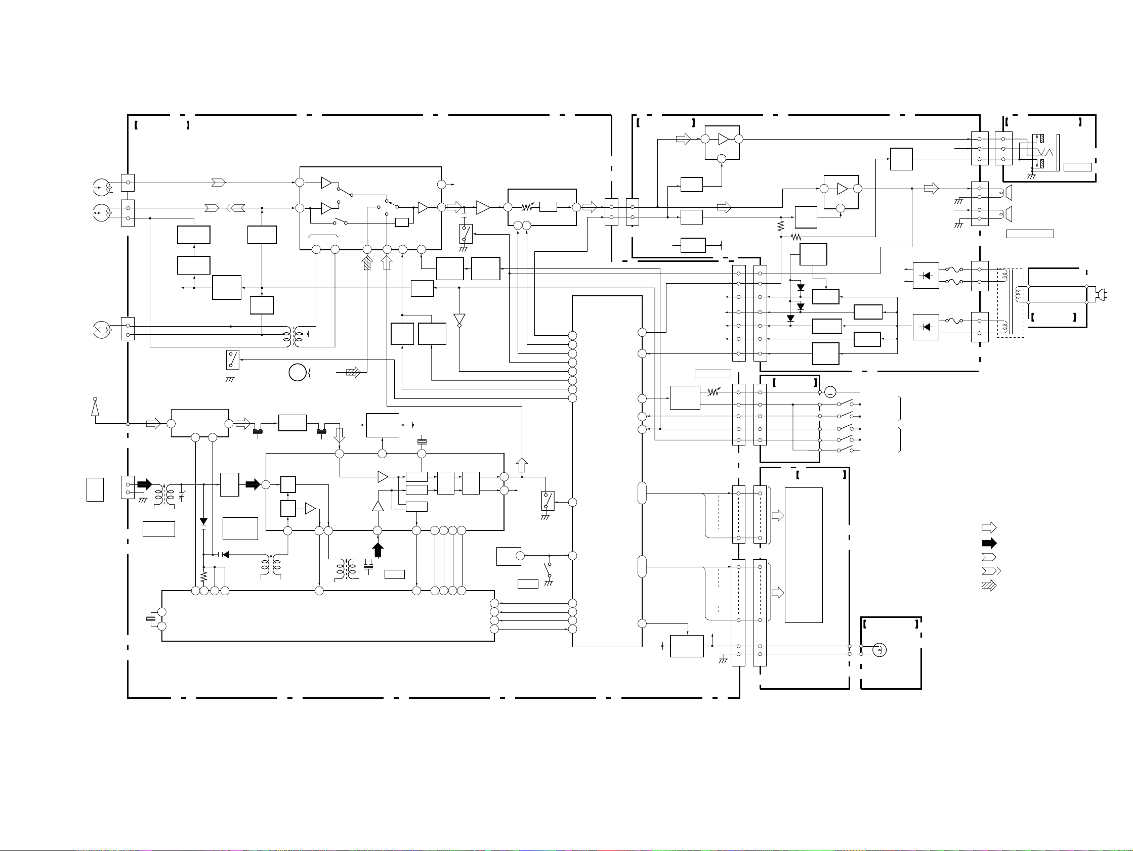
5-4. BLOCK DIAGRAM — MAIN SECTION —
CFD-C1000
HP301
PLAYBACK HEAD
(DECK-A)
L-CH
L-CH
HRP301
RECORD/PLAYBACK
HEAD
(DECK-B)
HE301
ERASE HEAD
(DECK-B)
ANT1
FM TELESCOPIC
ANTENNA
JK303
AM
EXT
ANT
MAIN BOARD (2/2)
CN301
3
CN502
5
4
R-CH
CN303
2
1
FM TUNER UNIT
8
L4
AM ANT
2
1
TC2
L4,TC2
AM
TRACKING
X1
7.2MHz
X IN
1
X OUT
23
REC/PB SW
Q102,103
REC/PB SW
Q302
BEAT CUT
FE1
16 18 19 20
FM IN
Q316
43
PD1
REC/PB
SW
Q303,304
1
AM RF
AMP
Q8
FREQUENCY
CONVERAGE
A IN
AOUT
REC MUTE
Q125
REC SW
Q314
CD SECTION
CF1 CF2
RF IF AMP
IF AMP,DET,MPX
AM
21
MIX
AM
L5
AM OSC
OSC
L5
AM
TAPE REC/PB PRE AMP
IC301
A-L
1
B-L
32
BIAS
TR-C CD-L TU-LTR-B
30
29
L301
+7.5V
CD L-CH
1
Q1
IC2
OSC AM MIX AM IF
23
24 2
15 12 8
AM IN
PLL
IC3
12 10 27 28
FM POWER
+FM
CONTROL
1 8
AM IFT
T2
CF3
POWER BOARD
5
ELECTRONIC VOLUME
15
14
DECK A/B
CONTROL
Q305,306
Q311
CF4
MPX MUTE
R-CH
Q301
LINE AMP
IC303
75
MEGA BASS
Q121
DECK A/B
SELECTOR
Q313
L OUT
R OUT
13
14
OUTR
OUTL
ALC
NOR A/B
REC SW
Q308
CD ON
RADIO ON
SWITCH
SWITCH
Q312
Q14
7
FM+BFM IF
+10V
FM DET
AM DET
IF
IC304
L IN L OUT
SDA SCL
9 10
R-CH
TONE
83
22
21
34
88
86
20
Q123
84
2 8
CN313 CN313
SYSTEM CONTROL
IC801(2/2)
SYSTEM
MUTE
SCL
4
SDA
MEGA BASS
REC
RADIO LED
CD LED
BEAT CONT
TUNER MUTE
343
POWER
SW OUT
MOTOR
CONT
OUT
SEG26
SEG11
I
4
82
1AC CHK
98
99TC A
100TC B
80
I
65
HP5V
MUTE
Q380
MUTE
Q382
+5V REG
IC309
MOTOR
CONTROL
Q309,310
M9V
+10V
+7.5V
TAPE SPEED
SFR301
MUTE
2
+5V
SEG26
HEADPHONE AMP
7
+10V
12
11
5
2
4
9
10
2
4
5
7
6
1
IC308
12
11
5
2
4
9
10
CN314CN314
2
4
5
7
6
CN305CN305
CN801
1
POWER
MUTE
Q321
ERROR
Q322,323
MD BOARD
LCD BOARD
POWER AMP
11 2
DET
+9V REG
Q380
+7.5V REG
Q326
VOLTAGE
CHECK
Q328
IC305
MUTE
5
(CAPSTAN/REEL)
M
+10V REG
Q325
+5V REG
IC306
M301
S1 (MOTOR)
S2 (PLAY)
S3 (PLAY)
S4 (REC)
S5 (MOTOR)
POWER
MUTE
Q381
+15V
-15V
DECK-A
DECK-B
RECT
D330
RECT
D327
R-CH
R-CH
F302
F303
F301
CN308
CN307
CN306
HEADPHONE BOARD
4
4
2
2
1
1
CN308
+
–
+
–
SPEAKER IMP.6Ω
PT1
POWER
TRANSFORMER
3
1
2
1
SP901
SPEAKER (L-CH)
SP902
SPEAKER (R-CH)
JK301
AC BOARD
JK302
PHONES
~
AC IN
• Signal path
: FM
: AM
: PB
: REC
: CD
• R-ch : same as L-ch.
T2
AM IF
10 11 12 20 64
SEG10
SEG0
COM3
COM0
I
I
64
I
50
23LED VDD
LED POWER
+10V
CONTROL
Q811,812
IF IN
9 10 11
FM ST
AM/FM
RESET
3
IC802
S301
RESET
SD
SD/IN
CLK
3
CE
4
DI
5
6
DO
38
15
17
14
16
RESET
CE OUT
DATA OUT
CLOCK
DO IN
+9.5V
SEG11
SEG10
SEG0
COM3
COM0
CN802
16
16
1
1
15
15
16
16
17
17
CN802
LIQUID
CRYSTAL
DISPLAY
PANEL
LCD801
LAMP BOARD
LCD BACK LIGHT
LP801-803
04
– 19 – – 20 –
 Loading...