

Page 1
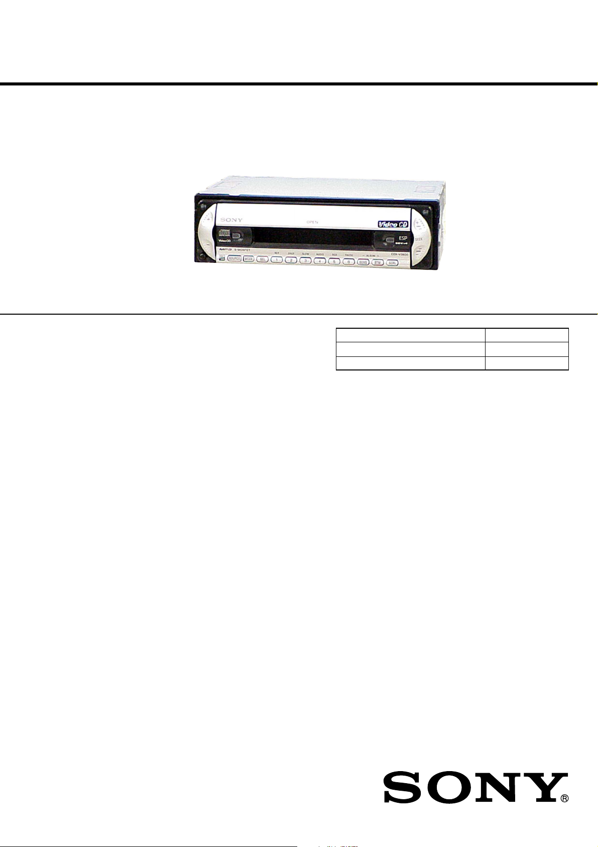
CDX-V3800
SERVICE MANUAL
Ver. 1.3 2006.05
• The tuner and CD sections have no adjustments.
SPECIFICATIONS
E Model
Chinese Model
Model Name Using Similar Mechanism NEW
CD Drive Mechanism Type MG-611MM-186//K
Optical Pick-up Name KSS1000E
CD player section
Signal-to-noise ratio 90 dB
Frequency response 10 – 20,000 Hz
Wow and flutter Below measurable limit
Signal format system PAL/NTSC
Tuner section
FM
Tuning range FM tuning interval:
50 kHz/200 kHz
switchable
87.5 – 108.0 MHz
(at 50 kHz step)
87.5 – 107.9 MHz
(at 200 kHz step)
Aerial terminal External aerial connector
Intermediate frequency 10.7 MHz/450 kHz
Usable sensitivity 9 dBf
Selectivity 75 dB at 400 kHz
Signal-to-noise ratio 67 dB (stereo),
69 dB (mono)
Harmonic distortion at 1 kHz
0.5% (stereo),
0.3% (mono)
Separation 35 dB at 1 kHz
Frequency response 30 – 15,000 Hz
AM
Tuning range AM tuning interval:
9 kHz/10 kHz switchable
531 – 1,602 kHz
(at 9 kHz step)
530 – 1,710 kHz
(at 10 kHz step)
Aerial terminal External aerial connector
Intermediate frequency 10.7 MHz/450 kHz
Sensitivity 30 µV
Power amplifier section
Outputs Speaker outputs
(sure seal connectors)
Speaker impedance 4 – 8 ohms
Maximum power output 52 W × 4 (at 4 ohms)
General
Outputs Audio output terminals (front, rear/sub switchable)
Video output terminal
Power aerial relay control terminal
Power amplifier control terminal
Inputs AUX IN terminal
Parking break control terminal
Aerial input terminal
Tone controls Low:
±10 dB at 60 Hz (XPLOD)
Mid:
±10 dB at 1 kHz (XPLOD)
High:
±10 dB at 10 kHz (XPLOD)
Power requirements 12 V DC car battery
(negative earth)
Dimensions Approx. 178 × 50 × 179 mm (w/h/d)
Mounting dimensions Approx. 182 × 53 × 161 mm (w/h/d)
Mass Approx. 1.2 kg
Supplied accessories Parts for installation and connections (1 set)
Front panel case (1)
Card remote commander RM-X158
Design and specifications are subject to change without
notice.
9-879-406-04
2006E04-1
© 2006.05
FM/AM MULTI MEDIA PLAYER
Sony Corporation
eVehicle Division
Published by Sony Techno Create Corporation
1
Page 2
CDX-V3800
Ver. 1.2
SERVICE NOTES
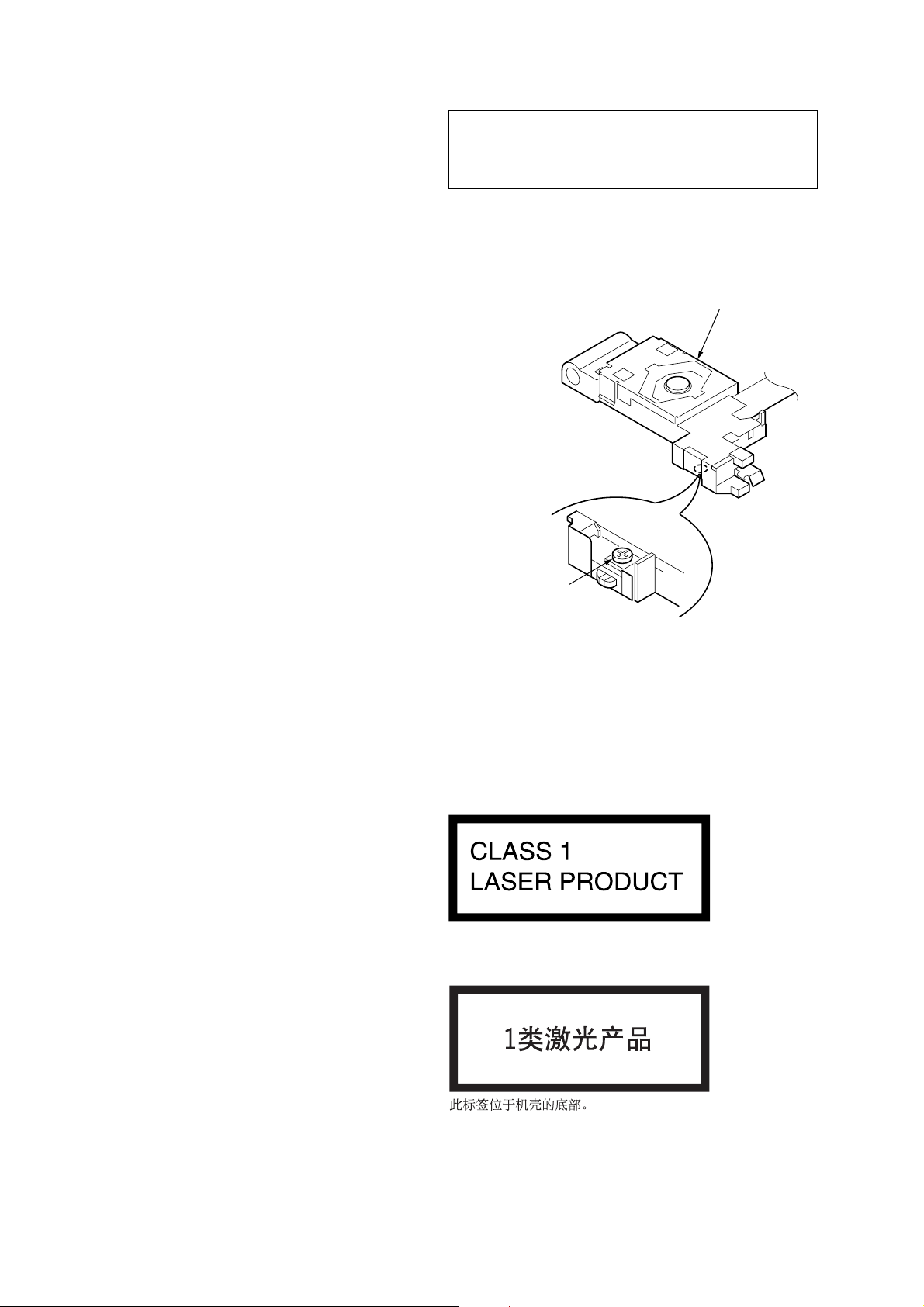
NOTES ON HANDLING THE OPTICAL PICK-UP BLOCK
OR BASE UNIT
The laser diode in the optical pick-up block may suffer electrostatic
breakdown because of the potential difference generated by the
charged electrostatic load, etc. on clothing and the human body.
During repair, pay attention to electrostatic breakdown and also use
the procedure in the printed matter which is included in the repair
parts.
The flexible board is easily damaged and should be handled with
care.
NOTES ON LASER DIODE EMISSION CHECK
The laser beam on this model is concentrated so as to be focused on
the disc reflective surface by the objective lens in the optical pickup block. Therefore, when checking the laser diode emission, observe from more than 30 cm away from the objective lens.
Notes on Chip Component Replacement
•Never reuse a disconnected chip component.
• Notice that the minus side of a tantalum capacitor may be damaged by heat.
CAUTION
Use of controls or adjustments or performance of procedures
other than those specified herein may result in hazardous
radiation exposure.
If the optical pick-up block is defective, please replace the whole
optical pick-up block.
Never turn the semi-fixed resistor located at the side of optical
pick-up block.
optical pick-up
semi-fixed resistor
TEST DISCS
This set can playback CD-R and CD-ROM discs. The following
test discs should be used to check the capability:
CD-R test disc TCD-R082LMT (Part No. J-2502-063-1)
CD-RW test disc TCD-W082L (Part No. J-2502-063-2)
E model
This label is located on the bottom of the chassis.
Chinese model
SAFETY-RELATED COMPONENT W ARNING!!
COMPONENTS IDENTIFIED BY MARK 0 OR DOTTED LINE
WITH MARK 0 ON THE SCHEMATIC DIAGRAMS AND IN
THE PARTS LIST ARE CRITICAL TO SAFE OPERATION.
REPLACE THESE COMPONENTS WITH SONY P ARTS WHOSE
PART NUMBERS APPEAR AS SHOWN IN THIS MANUAL OR
IN SUPPLEMENTS PUBLISHED BY SONY.
2
Page 3
CDX-V3800
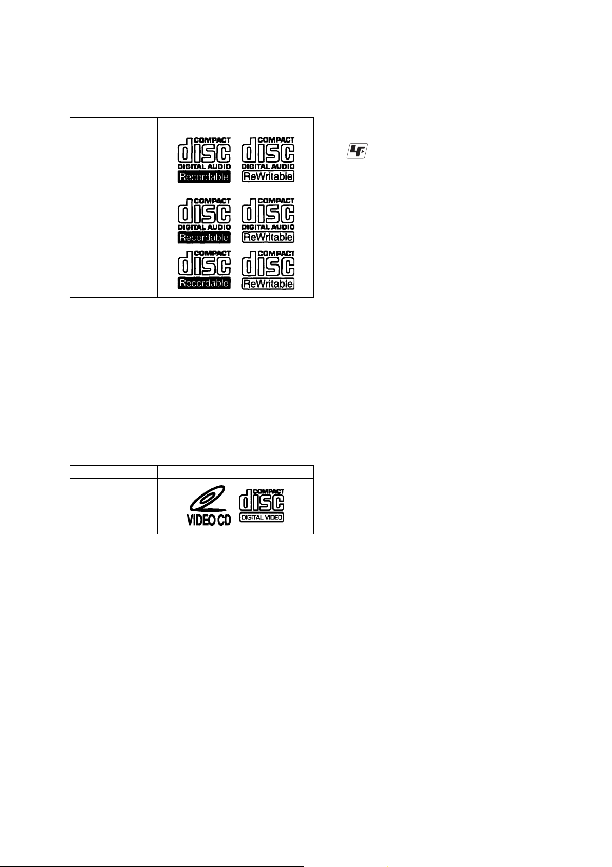
Notes on CD-Rs (recordable CDs)/CD-RWs (rewritable
CDs)
This unit can play the following discs:
Type of discs Label on the disc
Audio CD
MP3 files
• Some CD-Rs/CD-RWs (depending on the equipment used for
its recording or the condition of the disc) may not play on this
unit.
• You cannot play a CD-R/CD-RW that is not finalized∗.
• You can play MP3 files recorded on CD-ROMs, CD-Rs, and
CD-RWs.
• A CD-R/CD-RW to which a session can be added can be played.
z
UNLEADED SOLDER
Boards requiring use of unleaded solder are printed with the lead
free mark (LF) indicating the solder contains no lead.
(Caution: Some printed circuit boards may not come printed with
the lead free mark due to their particular size.)
: LEAD FREE MARK
Unleaded solder has the following characteristics.
• Unleaded solder melts at a temperature about 40°C higher than
ordinary solder.
Ordinary soldering irons can be used but the iron tip has to be
applied to the solder joint for a slightly longer time.
Soldering irons using a temperature regulator should be set to
about 350°C.
Caution: The printed pattern (copper foil) may peel away if the
heated tip is applied for too long, so be careful!
• Strong viscosity
Unleaded solder is more viscous (sticky, less prone to flow)
than ordinary solder so use caution not to let solder bridges
occur such as on IC pins, etc.
• Usable with ordinary solder
It is best to use only unleaded solder but unleaded solder may
also be added to ordinary solder.
∗ A process necessary for a recorded CD-R/CD-RW disc to be
played on the audio CD player.
Notes on Video CDs
This unit can play the following discs:
Type of discs Label on the disc
Video CD
VCD
A compact disc that contains moving pictures.
The picture data uses the MPEG 1 format (Video CD), worldwide
standards of digital compression technology.
Video CDs also contain compact audio data.
Sounds outside the range of human hearing are compressed while
the sounds we can hear are not compressed.
3
Page 4

CDX-V3800
TABLE OF CONTENTS
1. GENERAL
Location of Controls................................................................ 5
Connections ............................................................................. 5
2. DISASSEMBLY
2-1. Sub Panel (1) Assy .............................................................. 8
2-2. CD Mechanism Block ......................................................... 8
2-3. Main Board ......................................................................... 9
2-4. Chassis (T) Sub Assy .......................................................... 9
2-5. Roller Arm Assy................................................................10
2-6. Chassis (OP) Assy.............................................................10
2-7. Optical Pick-up ................................................................. 11
2-8. SL Motor Assy (M902) .....................................................11
2-9. LE Motor Assy (M903)..................................................... 12
2-10. Servo Board....................................................................... 12
3. DIAGRAMS
3-1. Block Diagram –CD Section–........................................... 13
3-2. Block Diagram –Main Section–........................................14
3-3. Block Diagram –Display Section–....................................15
3-4. Circuit Boards Location .................................................... 15
3-5. Printed Wiring Boards –CD Mechanism Section–............ 17
3-6. Schematic Diagram –CD Mechanism Section (1/2)– ....... 18
3-7. Schematic Diagram –CD Mechanism Section (2/2)– ....... 19
3-8. Printed Wiring Boards –Main Section– ............................ 20
3-9. Schematic Diagram –Main Section (1/3)– ........................21
3-10. Schematic Diagram –Main Section (2/3)– ........................22
3-11. Schematic Diagram –Main Section (3/3)– ........................23
3-12. Printed Wiring Board –Display Section– .......................... 24
3-13. Schematic Diagram –Display Section–............................. 25
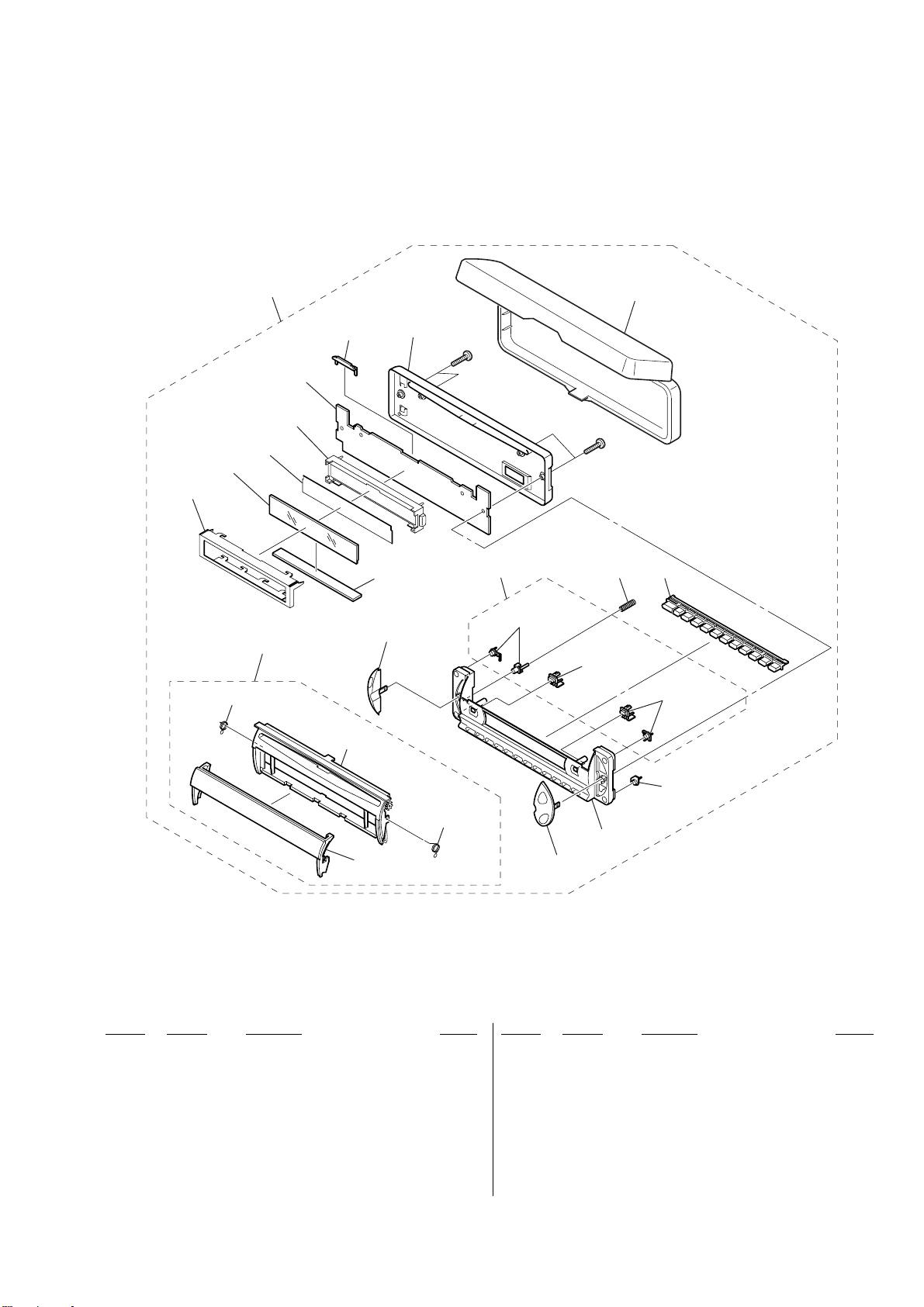
4. EXPLODED VIEWS
4-1. Main Section ..................................................................... 32
4-2. Front Panel Section ........................................................... 33
4-3. CD Mechanism Section (1) ...............................................34
4-4. CD Mechanism Section (2) ...............................................35
4-5. CD Mechanism Section (3) ...............................................36
4-6. CD Mechanism Section (4) ...............................................37
5. ELECTRICAL PARTS LIST......................................... 38
4
Page 5
SECTION 1
GENERAL
CDX-V3800
This section is extracted
from instruction manual.
Location of controls
Refer to the pages listed for details.
ATT OFF
DSPL
SLOW
SOURCE MODE
SEL
123456
a Volume +/– button
b ATT (attenuate) button 17
c DSPL (display mode change) button
11, 14
d OPEN/EJECT shutter 11, 12
e Display window
f EQ3 button 18
g OFF (Stop/Power off) button*
18
h SEEK +/– button
Radio:
To t une in stations automatically/find a
station manually.
CD/VCD:
To s ki p tracks/fast-forward, reverse a tr ack.
i (front panel release) button 10
j SOURCE (Power on/Radio/CD/AUX)
button
To s el ect the source.
k MODE button
To c hange the operation.
l SEL (select) button
To s el ect items.
m RESET button (located on the front side of
the unit, behind the front pa nel ) 9
1
10, 12,
AUDI O OSD PAU SEREP SHUF
SENS
n Number buttons 17
Radio:
To s t o r e stations /r eceive store d stati on s.
CD/VCD:
(1): REP 15
(2): SHUF 15
(3): SLOW 13
(4): AUDIO 14
(5): OSD 19
(6): PAUSE 12, 13
o Frequency select switch (located on the
bottom of the unit)
See “Frequency select switch” in the
Installation/Connections manual.
p SENS/ALBUM – button 12, 16
q BTM/ALBUM + button 12, 15
r SCRL (scroll) button 14
s Receptor for the card rem ote
commander
*1 Warning when installing in a car without an
ACC (accessory) position on the ignition switch
After turning off the ignition, be sure to press and
hold (OFF) on the unit until the display disappears.
Otherwise, the display does not turn off and this causes
battery drain.
–
ALBUM
EQ3
+
BTM SCRL
SEEK
CDX-V3800
Card remote commander RM-X158
1
OFF
2
SOURCE
3
4
5
6
7
The corresponding buttons of the card
remote commander control the same
functions as those on this unit.
a OFF button
b SOURCE button
c PBC button 14
d ENTER button 14
e < (.)/, (> ) buttons
f DSPL button
g VOL (+/–) button
h ATT button
i SEL button
j MODE button
k O (return) button 14
l M (+)/m (–) button s 1 4
m SCRL button
n Number buttons
Note
If the display disappears by pressing
be operated with the card remote commander unless
(SOURCE)
to activate the unit first.
Tip
For details on how to replace the battery, see
“Replacing the lithium battery” on page 20.
SEL MODE
PBC
+
ENTER
–
DSPL
REP SHUF SLOW
132
465
+
VOL
–
on the unit is pressed, or a disc is inserted
8
AT T
9
q;
qa
qs
SCRL
qd
PA US EOSDAUDIO
qf
(OFF)
, it cannot
Selecting an album with the card
remote commander
Album can be skipped using M (+)/m (–) on the
card remote commander.
To Press
Skip albums*
–Album selection
*
Available only when an MP3 file is played.
Skipping tracks continuously
Press once < or , on the card remote
commander, then press again within 2 seconds
and hold.
M or m [once for each
album]
To con tinuously skip
albums, press and hold
either button.
4
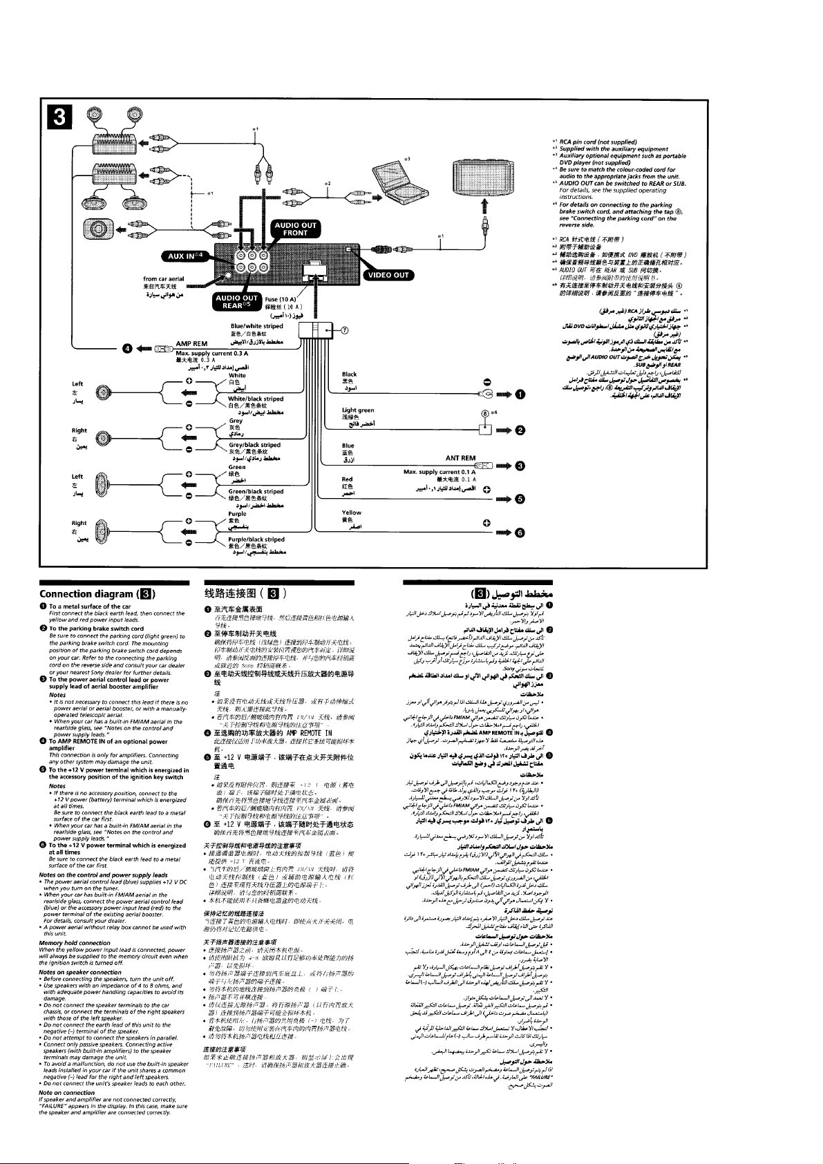
CONNECTIONS
2
A
B
AUDIO OUT FRONT
VIDEO OUT
AUDIO
OUT REAR
5
5
Page 6
CDX-V3800
6
Page 7
SECTION 2
DISASSEMBLY
Note : This set can be disassemble according to the following sequence.
SET
2-1. SUB PANEL (1) ASSY
(Page 8)
2-2. CD MECHANISM BLOCK
(Page 8)
CDX-V3800
2-3. MAIN BOARD
(Page 9)
2-7. OPTICAL PICK-UP
(Page 11)
2-4. CHASSIS (T) SUB ASSY
(Page 9)
2-5. ROLLER ARM ASSY
(Page 10)
2-6. CHASSIS (OP) ASSY
(Page 10)
2-8. SL MOTOR ASSY (M902)
(Page 11)
2-10. SERVO BOARD
(Page 12)
2-9. LE MOTOR ASSY (M903)
(Page 12)
7
Page 8
CDX-V3800
s
)
Note : Follow the disassembly procedure in the numerical order given.
2-1. SUB PANEL (1) ASSY
3
two claws
1
two
screws
(+PTT 2.6
x
6)
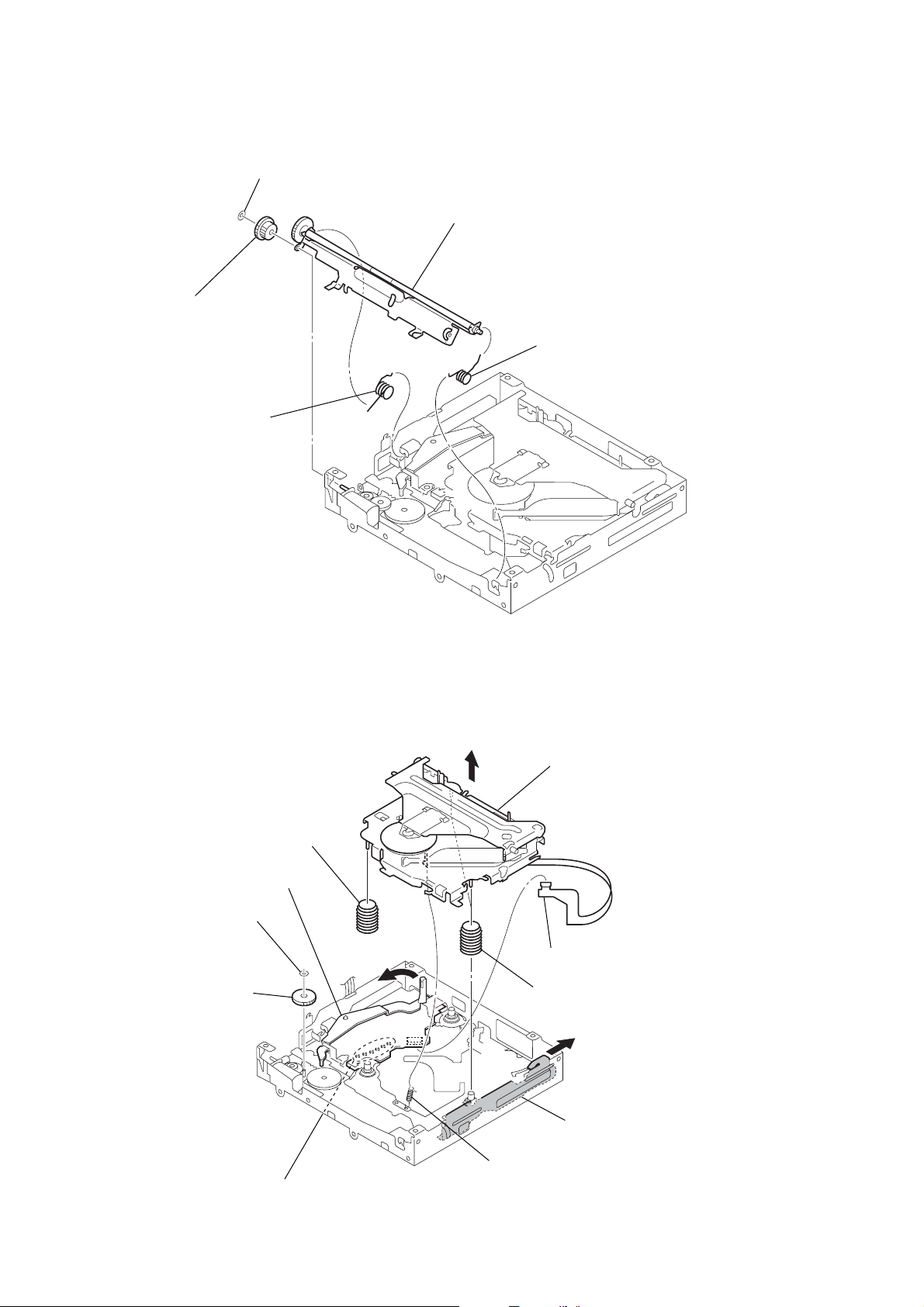
2-2. CD MECHANISM BLOCK
6
CD mechanism block
SERVO board
3
4
sub panel (1) assy
8
bracket (CD)
2
7
two
screws
(+PTT 2.6
two claw
x
6)
5
4
CN751 (26core)
2
screw
(+PTT 2.6
x
6)
CN401
(2P)
1
screw
(+PTT 2.6
x
6
8
Page 9
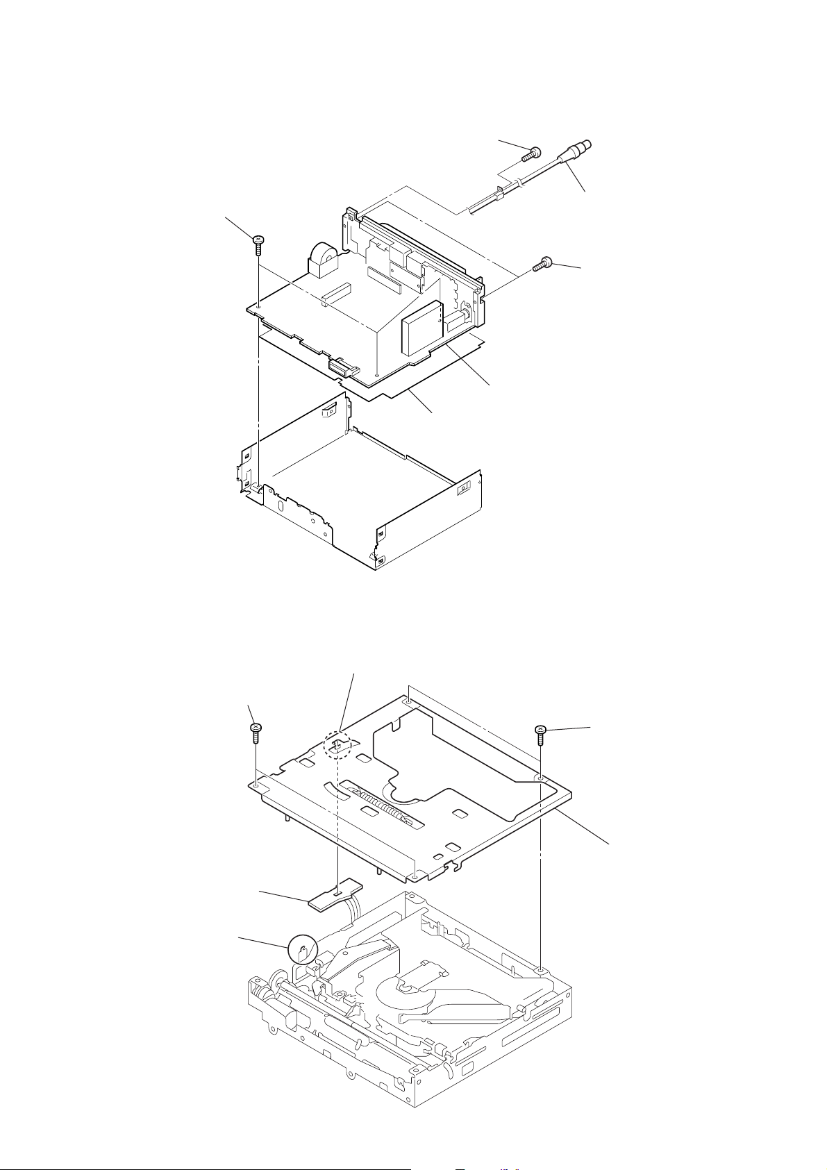
2-3. MAIN BOARD
d
1
three screws
(+BTT )
5
screw
(+PTT 2.6
4
insulating sheet
x
8)
3
MAIN board
6
connection (video out) cor
2
two
screws
x
(+PTT 2.6
8)
CDX-V3800
2-4. CHASSIS (T) SUB ASSY
2
two
screws
(+P 1.7
5
SENSOR board
3
claw
x
2.2)
4
claw
1
two
screws
x
(+P 1.7
6
2.2)
chassis (T) sub assy
9
Page 10
CDX-V3800
2-5. ROLLER ARM ASSY
4
gear (RA1)
1
spring (RAL)
3
washer (1.1-2.5)
5
roller arm assy
2
spring (RAR)
2-6. CHASSIS (OP) ASSY
0
coil spring (damper)
4
washer
5
gear (LE1)
lever (D)
6
8
qa
chassis (OP) assy
1
CN500 (16P)
9
two coil springs (damper)
7
slider (R)
10
2
Remove the six solderings.
3
tension coil spring (KF60)
Page 11
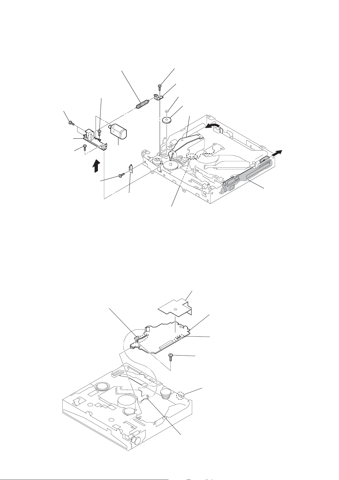
2-7. OPTICAL PICK-UP
)
5
claw
2
chucking arm sub assy
1
tension coil spring (CHKG
7
optical pick-up
CDX-V3800
2-8. SL MOTOR ASSY (M902)
6
main shaft
4
rack (SL)
3
screw
(+B 1.4
x
5)
2
SL motor assy (M902)
1
screw
(+P 1.4
x
1.8)
11
Page 12
CDX-V3800
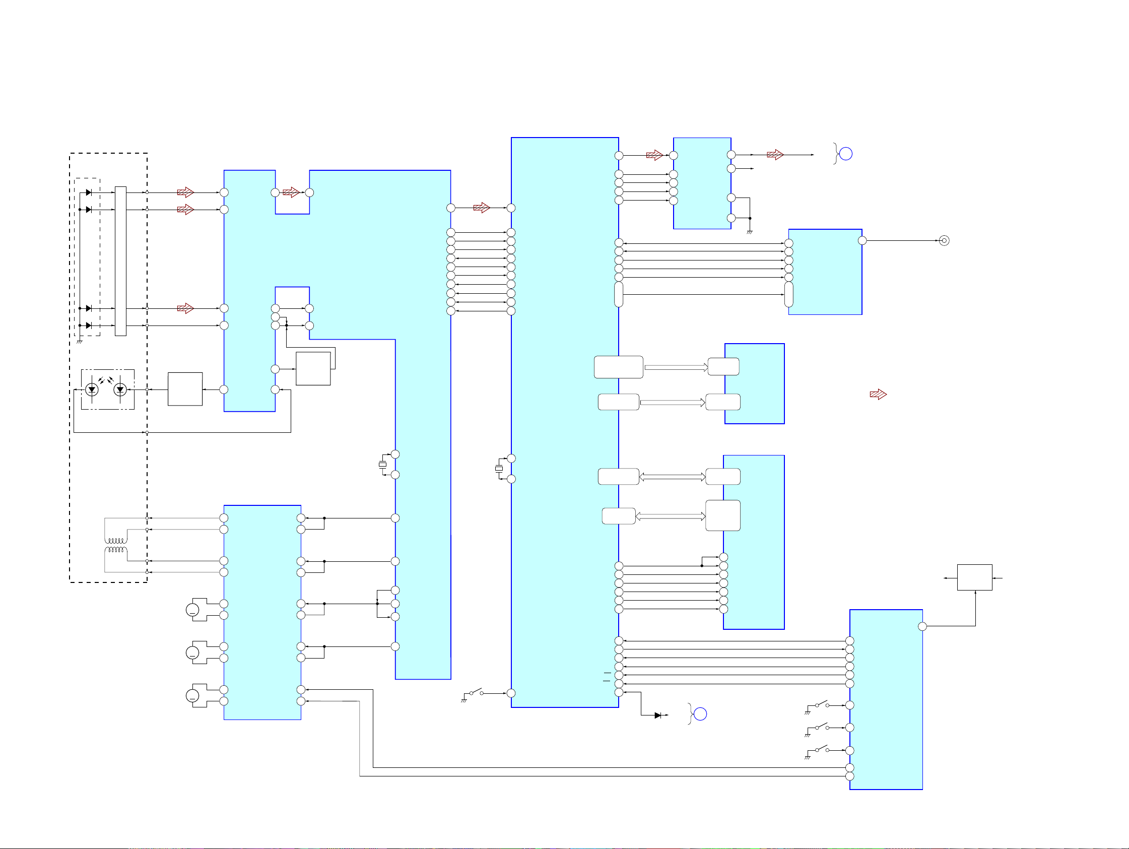
2-9. LE MOTOR ASSY (M903)
qf
two toothed lock
(+M 1.4
bracket (LEM-N)
qs
(+M 1.7
screw
x
)
screws
2.5)
6
screw
(+P 1.7
x
qa
(+M 1.7
qd
2.2)
screw
0
gear (LE) assy
x
2.5)
qg
LE motor assy
(M903)
7
leaf spring (LE)
8
screw
(+M 1.7
9
bearing (LEB-N)
2
washer
gear (LE1)
3
lever (D)
x
2.5)
4
5
slider (R)
2-10. SERVO BOARD
2
Remove the eight solderings.
1
Remove the two solderings.
1
shield sheet
7
SERVO board
3
Remove the three solderings.
5
precision
(+P 1.7
x
screw
2.2)
12
4
CN500 (16P)
6
claw
Page 13
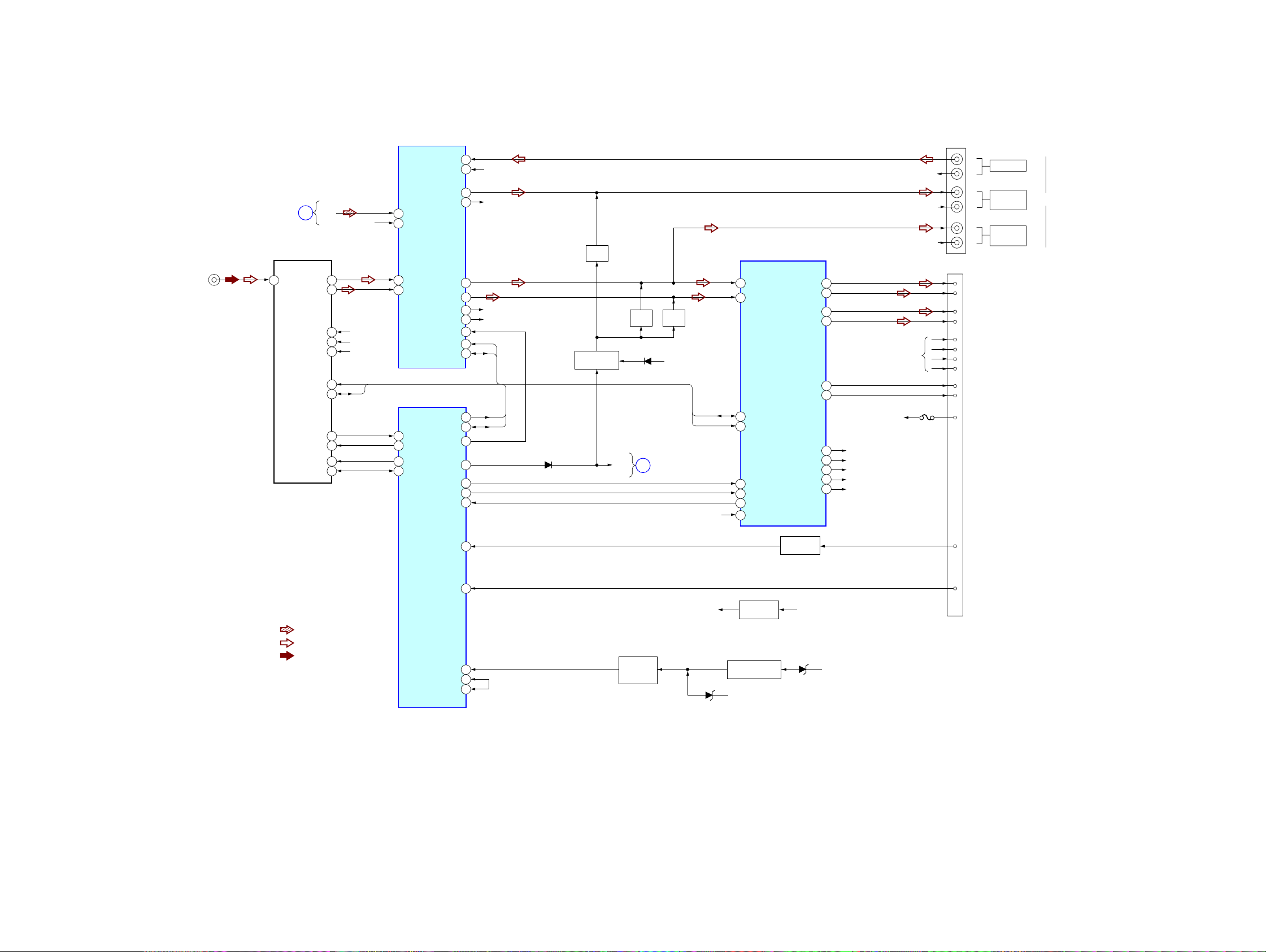
3-1. BLOCK DIAGRAM — CD SECTION —
CDX-V3800
SECTION 3
DIAGRAMS
DETECTOR
PD1
PD2
E
F
LASER DIODE
I-V AMP
PD LD
PD1
PD2
2
1
3
14
12
DIGITAL
MODULATOR
DIN
LRCK
BCKIN
SCKI
DEEMP
IC700
LOUT
ROUT
MUTE
FORMAT
45•25–18•
8–1•48•17
29•31•33•35
•38•30•42–44
9
6
10
13
16M SDROM
A18
DQ0
DQ7
IC200
A0
I
I
R-CH
28
29
15
14
9
17
I
24
VIDEO SIGNAL
PROCESSOR
VSYNC
HSYNC
CLK
MODEB
SLEEP
P0
I
P7
CD-L
IC400
MAIN
A
SECTION
(Page 14)
32
CVBS/Y
• R-ch is omitted due to same as L-ch.
• Siganal Path
: CD PLAY
CN401
(VIDEO OUT)
DIGITAL SIGNAL PROCESSOR
IC100
77
AU DATA
78
AU LRCK
79
AU BCK
76
ROMA0
I
ROMA18
ROMD0
I
ROMD7
CLK27 OUT
AU XCK
103
DEEMP
56
VSYNC
55
HSYNC
69
70
PLA NTSC
54
V RST
64
YC0
I
57
YC7
29–32•34•38•40•42
•41•39•33•35•44•
43•45–49
27•25•23•21•22
•24•26•28
I
ROMA0-ROMA18
ROMD0-ROMD7
2
BD
3
E
F
LD
AUTOMATIC
POWER
CONTROL
Q501
5
E
6
F
13
LD
FEO
TZCRFM
TEO
LON
52
RF AMP,
DIGITAL SERVO,
IC500
9
46
48
24
12
PD
EQ0
AC
RFI
51
FEN
8
TEN
49
LASER ON
CONTROL
SWITCH
Q502
DOUTA
LRCK
WFCK
DCK
EFLAG
SUBSYQ
BUSY
RESETX
R/W
DIN/OUT
MCK
35
36
34
37
38
31
30
29
28
27
26
96
97
50
98
102
81
80
82
83
84
85
CD DATA
CD LRCK
BATTLOW
CD BCLK
CD XCK
SUBSYQ
BUSY
XRESET
R/W
DI/DO
MCK
PICK-UP BLOCK
(KSS1000E)
2-AXIS DEVICE
(FOCUS)
(TRACKING)
OPTICAL
MONOUT
FCS+
FCS–
TRK+
TRK–
M902
(SLED)
M901
(SPINDLE)
M903
(LOADING)
16M SDROM
XI
X541
16.934MHz
FOCUS/TRACKING COIL DRIVE,
SLED/SPINDLE/LOADING
MOTOR DRIVE
IC600
16
VO4(–)
15
VO4(+)
VO3(+)
17
VO3(-)
18
14
M
M
M
VO1(+)
13
VO1(-)
VO2(+)
12
VO2(-)
11
10
VOL(+)
9
VOL(-)
IN1(–)
OUT1
IN2(–)
OUT2
IN3(–)
OUT3
IN4(–)
OUT4
FWD
REV
3
4
6
7
23
22
26
25
1
28
42
43
20
22
17
18
19
21
XO
SD OUT
CLV OUT
JUMP0
TDOUT
SDIN
FD OUT
X401
27MHz
S901
(LIMIT)
65
CLKIN
DA0
17–20•16–12
66
CLKIO
LIMIT
92
DA10
DD0
DD15
I
•111•110
116–123•6–2
I
•126–124
DQMO
114
9 15
WE B
10 16
CAS B
11 17
RASO B
112 19
BAO
127 35
RAMCLK
SI
91
SO
93
SCK
99
RESET B
88
SP
89
MP
113
MUTE
RAMA0-RAMA10
RAMD0-RAMD15
MUTE
D701
21–24•
27–32•20
2•3•5•6•8•
9•11•12•39•
40•42•43•45
•46•48•49
MAIN
B
SECTION
(Page 14)
IC300
A0
I
A10
DQ0
I
DQ15
14
LDON
36
UDQM
WE
CAS
RAS
BA
CLK
SW1
(DOWN)
SW2
(SELF)
SW3
(DISC IN)
SYSTEM CONTROL
CD SO
1990
CD SI
18
CD SCK
20
CD XRST
98
SP
54
MP
90
CD DSW
95
CD SELFSW
55
CD INSW
92
CD LOAD
93
EJECT
94
IC801 (1/3)
CD ON
BU+3.3V
87
CD POWER
CONTROL
Q701,703
U COM+3.3V
CDX-V3800
13 13
Page 14
CDX-V3800
3-2. BLOCK DIAGRAM — MAIN SECTION —
ELECTRONIC VOLUME
PJ601
(ANTENNA)
CD
SECTION
(Page 13)
(TUNER UNIT)
1
ANT
TUX601
E2P VDD
S-METER
TU MUTE
E2P SCL
E2P SDA
A
VCC
TU VDD
TU-SCL
TU-SDA
CD-L
L
R
10
11
15
13
14
16
17
4
3
6
7
R-CH
AU+8V
TU+5V
U COM+3.3V
SCL
SDA
9
8
7
6
45
15
25
24
IC401
OUTS2
OUTS1
C2
C1
B2
B1
VSM
TU ATT
EEP SCK
EEP SIO
OUTF2
OUTR2
OUTF1
OUTR1
MUTE
SYSTEM CONTROL
IC801 (2/3)
IIC SCK
IIC SIO
VOL ATT
LINE ATT
AP2
AP1
SCL
SDA
BEEP
STB
DIAG
5
3
17
18
23
22
25
24
29
30
31
33
34
6
1
5
31
56
R-CH
R-CH
R-CH (FRONT)
R-CH (REAR)
SCL
SDA
SCL
SDA
D702
MUTE
Q407
MUTE DRIVE
Q400,401
MUTE
MUTE
Q405
D400
B
MUTE
Q404
BATT
CD
SECTION
SDA
SCL
(Page 13)
BATT
12
11
2
4
16
22
25
35
POWER AMP
IN RR(FL)
IN RF(RL)
SDA
SCL
ACGND
STB
DIAG
VP
IC100
RF+
RF-
SW1
SW2
REG1
REG2
REG3
REG4
REG5
LF+
LF-
29
27
30
37
31
33
34
5
3
9
7
AU+8V
U-COM+3.3V
SERVO+3.3V
MECHA+6V
DISP+B
BATT
R-CH
R-CH
R-CH
R-CH
F900
CNP901
1
9
2
10
4
12
3
11
5
6
16
L
R
L
R
L
R
FL+
FL-
RL+
RL-
FR+
FRRR+
RR-
AMP-REM
ANT-REM
BATT
AUX IN
REAR
AUDIO OUT
FRONT
AUDIO OUT
PJ401
• R-CH is omitted due to same as L-CH.
• Signal Path
: CD PLAY
: FM
: AM
ACC IN
PAK BK
BU IN
UNI SI
UNI SO
15
7
ACC
PAK BK
Q601
ACC CHECK
Q900
AU+8V
D912
BATT
64
67
TU+5V
53
58
59
BACK-UP
DETECT
Q906,907
D915
TU+5V REG
BATTERY CHECK
Q902
BATT
CDX-V3800
1414
Page 15
CDX-V3800
)
3-3. BLOCK DIAGRAM — DISPLAY SECTION —
SYSTEM CONTROL
26
38
39
47
75
46
46
77
72
IC801 (3/3)
SHUT SW
KEYIN0
KEYIN1
KEY ACK
XKEY ON
DST SEL
DST SEL
RESET
DOOR SW
LCD SO
LCD SCK
LCD CE
SIRCS
U COM+3.3V
KEY MATRIX
S501-521,523
S800
FREQUENCY
SELECT
9K
10K
2
IN
DISPLAY
BOARD
RESET
IC802
OUT
D801
1
S522
(OPEN)
ACK ON
SWITCH
Q800
S802
RESET
3-4. CIRCUIT BOARDS LOCATION
LCD DRIVER
IC501
SEG3
3
|
I
28
64
DI
CL
29
27
65
CLK
63
CE
CE
62
IR RECEIVER
IC502
OUT
2
SEG50
COM4
|
COM1
DIMMER
DIMMER
50
•
51
I
54
1
IR
LCD501
LIQUID
CRYSTAL
DISPLAY
PANEL
LED
CONTROL
Q502
DISP+B
LED501,502
LCD
BACK LIGHT
()
LED504-518,
520-522,524,525
SENSOR board
DISPLAY board
SERVO board
SPEAKER board
tuner unit
(TUX601
MAIN board
X801
32.768kHz
X1A
79
X0A
80
82
X0
X1
83
X800
18.432MHz
CDX-V3800
15 15
Page 16
CDX-V3800
Ver. 1.3
• NOTE FOR PRINTED WIRING BOARDS AND SCHEMATIC DIAGRAMS
THIS NOTE IS COMMON FOR PRINTED WIRING
BOARDS AND SCHEMATIC DIAGRAMS.
(In addition to this, the necessary note is printed
in each block.)
For schematic diagrams.
Note:
• All capacitors are in µF unless otherwise noted. (p: pF)
50 WV or less are not indicated except for electrolytics
and tantalums.
• All resistors are in Ω and 1/
specified.
f
•
• C : panel designation.
Note: The components identified by mark 0 or dotted line
• A : B+ Line.
•Voltages and waveforms are dc with respect to ground
• CD mechanism section (1/2, 2/2)
no mark : CD PLAY
• Main (1/3), (2/3), (3/3) and Display sections
no mark : FM
: internal component.
with mark 0 are critical for safety.
Replace only with part number specified.
under no-signal (detuned) conditions.
(): AM
<>: CD PLAY
4
W or less unless otherwise
For printed wiring boards.
Note:
• X : parts extracted from the component side.
• Y : parts extracted from the conductor side.
a
•
• : Pattern from the side which enables seeing.
(The other layers' patterns are not indicated.)
Caution:
Pattern face side: Parts on the pattern face side seen from the
(Side B) pattern face are indicated.
Parts face side: Parts on the parts face side seen from the
(Side A) parts face are indicated.
: Through hole.
C
Q
These are omitted
EB
∗ : Impossible to measure
•Voltages are taken with a VOM (Input impedance 10 MΩ).
Voltage variations may be noted due to normal production tolerances.
•Waveforms are taken with a oscilloscope.
Voltage variations may be noted due to normal production tolerances.
• Circled numbers refer to waveforms.
• Signal path.
J : CD PLAY
F : FM
f : AM
E
CB
These are omitted
C
BE
These are omitted
• WAVEFORMS
— Servo Board — (MODE: CD PLA Y) — Main Board —
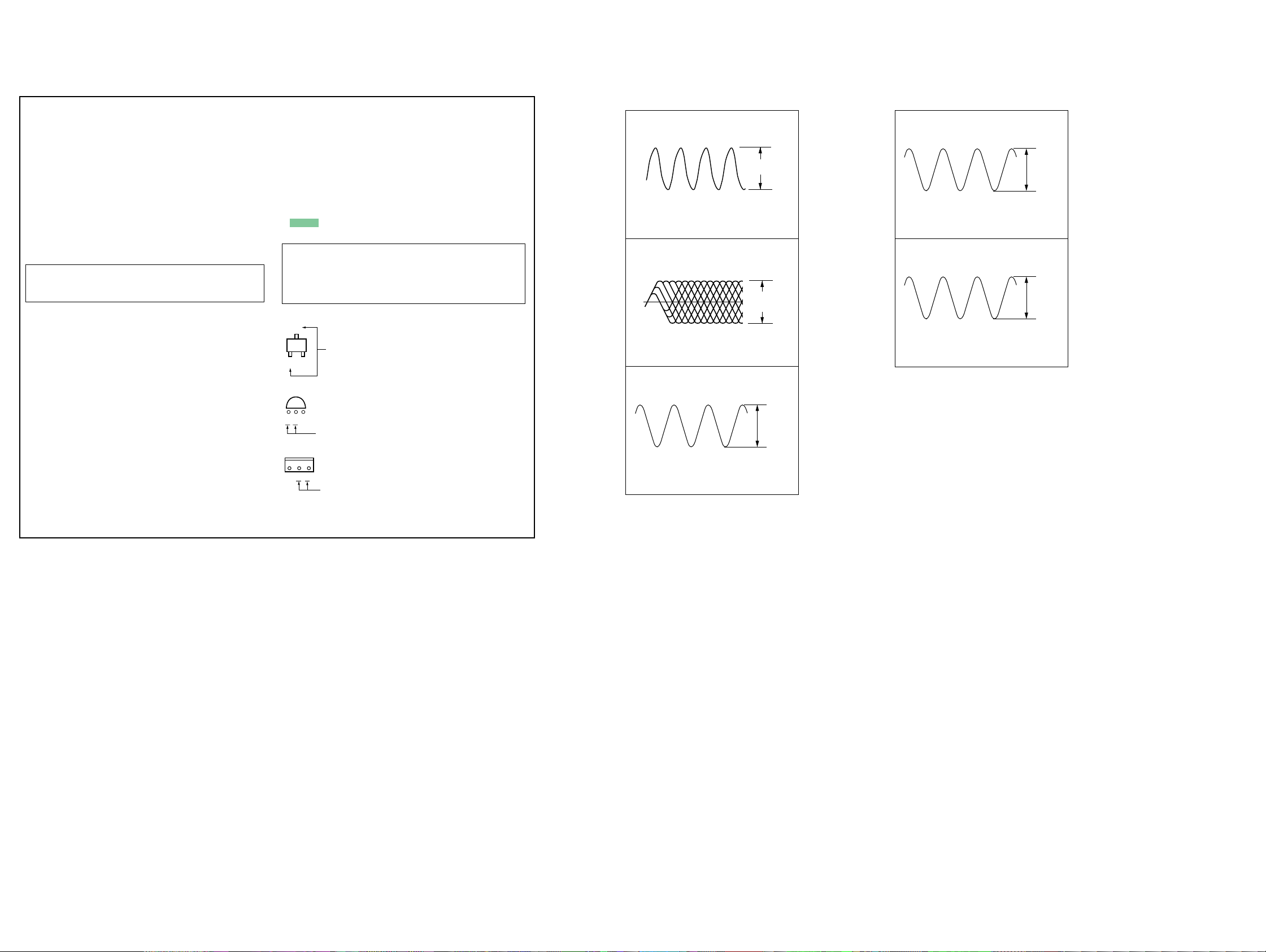
1
IC500 rd (XO)
16.9344 MHz
0.2 V/DIV, 0.2 µsec/DIV
2
IC500 ts (EQO)
0.5 V/DIV, 0.5
3
IC100 yg (CLKIN)
0.2 V/DIV, 0.2 µsec/DIV
µ
sec/DIV
27 MHz
1.8 Vp-p
0.8 V to
1.3 Vp-p
1.5 Vp-p
1
IC801 i; (XOA)
32.768 kHz
0.2 V/DIV, 20 µsec/DIV
2
IC801 is (X0)
18.432 MHz
0.5 V/DIV, 0.1
µ
sec/DIV
3.6 Vp-p
4.1 Vp-p
CDX-V3800
1616
Page 17
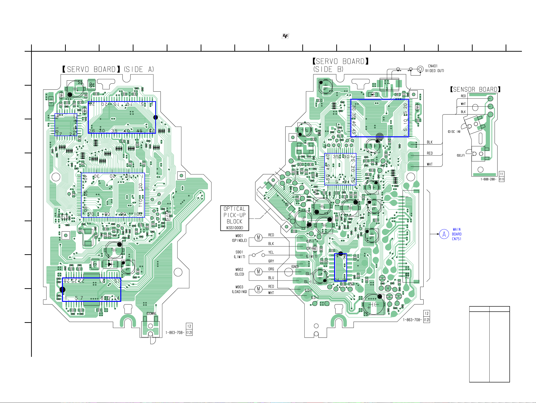
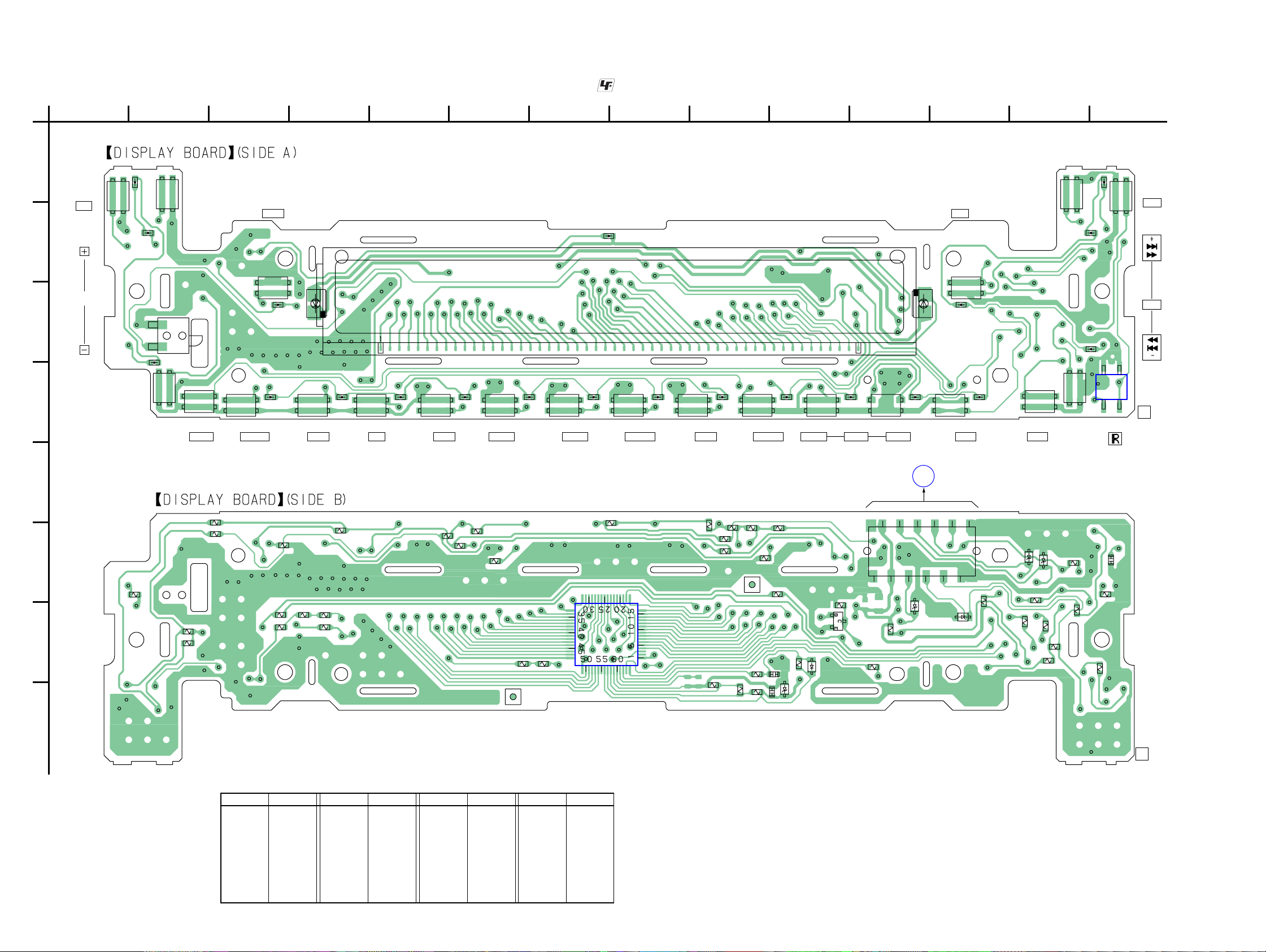
3-5. PRINTED WIRING BOARDS — CD MECHANISM SECTION — • Refer to page 15 for Circuit Boards Location. : Uses unleaded solder.
CDX-V3800
A
B
C
D
E
F
G
H
1
C201
R108
R626
R623
R606
R605
C404
RB111
R107
C159
D909
C408
R402
IC400
R106
TP131
IC101
FMA4
RB110
R162
R627
23456789101112 13 14 15
L401
R624
C623
R601
R102
C601
C401
C403
R161
C402
R401
R103
C132
R621
C621
C407
R603
R404
C133
X401
C603
D907
C410
RB107
C131
FB504
RB106
IC600
C305
RB103
L101
R405
C164
C406
C605
RB105
R163
RB104
C163
C161
D101
IC100
R178
R164
C102
C162
IC300
RB102
TP188
R167
C304
C312
TP189
C166
R629
R166
RB101
R180
R111
C303
R101
R168
R169
C708
R709
C112
C313
C181
C180
R632
C709
R109
R113
R114
C111
TP186
TP181
C182
R175
SW1
R112
TP184
C183
R181
RB113
TP187
TP185
RB112
R507
TP183
TP182
R509
R508
R110
Q501
FMA3
FMB3
TP559
TP542
TP558
C
N
50
C301
C302
C531
FMB5
X541
TP541
R541
C548
C545
R546
TP556
C546
TP557
TP552
0
TP560
FMB4
R551
C551
C508
TP555
TP551
TP62
TP59
R547
C501
TP63
TP64
TP57
TP58
TP61
C542
TP554
TP60
C547
C541
C543
TP553
R503
TP504
C540
C544
TP51
R545
R504
Q502
FB501
TP530
TP531
R542
R543
R544
C502
R502
C518
C506
TP503
D910
C701
C705
TP564
TP52
C519
R311
TP528
TP529
C703
C702
TP561
RB301
TP523
C507
R501
R176
C165
C707
R631
R630
R548
TP527
IC500
R505
R506
TP19
R312
C521
TP524
TP501
R172
IC700
C503
C517
R177
R708
TP562TP563
C505
R170
R171
R173
R704
C704
TP521
TP522
R707
TP525
C516
R515
C512
R511
C504
R702
R701
TP11
R513
C513
TP519
R165
TP10
C706
C509
R703
TP12
D906
C514
C511
C510
C515
C160
TP20
TP18
BP4
R622
TP622
C600
IC200
TP513
R512
C101
C103
R514
TP512
TP15
TP14
TP13
C400
TP22
BP1
CN401
FB503
R516
TP17
TP16
TP9
TP3
R625
BP2
R604
FB502
TP23
TP21
TP8
TP621
R602
TP5
RB108
R104
TP603
RB109
TP24
CN1
C520
R628
BP3
TP601
C405
R105
TP1
TP4
R600
R403
TP56
TP55
TP53
TP2
FMB6
C202
TP6
D908
3
SW
SW
(Page 20)
2
• Semiconductor
Location
Ref. No. Location
D101 G-3
D906 B-11
D907 B-2
D909 B-1
D910 F-9
I
CDX-V3800
IC100 E-3
IC200 B-11
IC300 B-3
IC400 C-2
IC500 D-10
IC600 H-2
IC700 G-10
Q501 E-5
Q502 E-9
17 17
Page 18
CDX-V3800
Ver. 1.3
• Refer to page 16 for Waveforms.
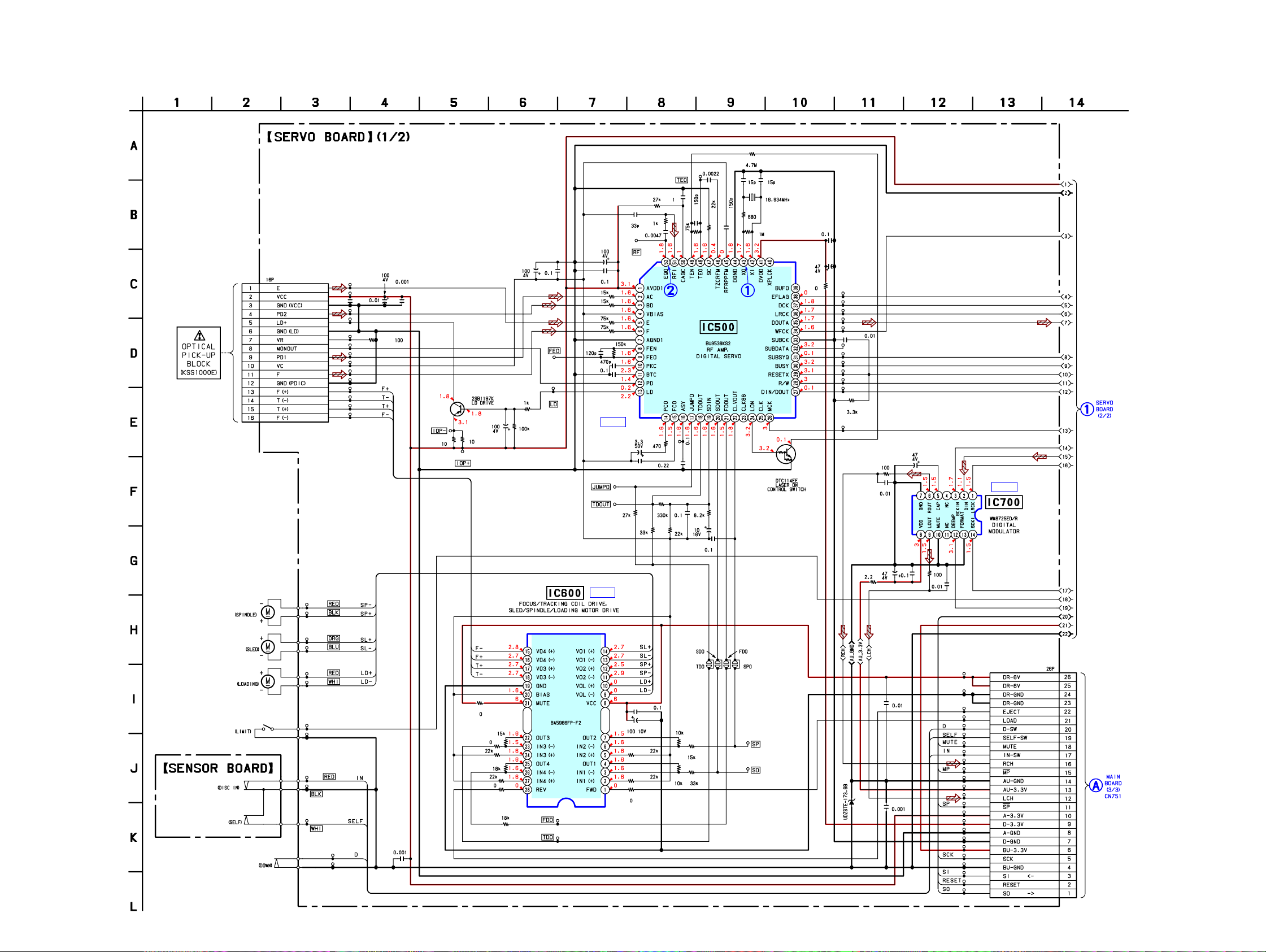
3-6. SCHEMATIC DIAGRAM — CD MECHANISM SECTION (1/2) — • Refer to page 26 for IC Block Diagrams. • Refer to page 27 for IC Pin Description of IC500.
CN500
TP551
TP552
C551
TP555
TP556
TP557
TP558
TP559
TP560
TP561
TP562
TP563
TP564
TP553
TP554
C501
R551
C508
TP504
R509
TP503
R508
Q501
C506
C517
R506
R507
C507
TP501
TP502
R501
R502
R503
R504
C503
C504
C505
C518
C502
R505
IC B/D
TP512
TP513
R512
C545
TP542
C511
R516
C512
R545
R546
C546
R511
R515
C544
TP541
C515
R514
TP511
R544
C513
R513
C514
C543
C542
C516
R543
IC500
C541
R547
C547 C548
R541
R542
X541
Q502
C531
FB501
C540
TP531
TP530
TP529
TP528
TP527
C521
TP526
TP525
TP524
TP523
TP522
TP521
R548
TP519
R709
C709
(Page 19)
C705
IC B/D
IC700
SW3
SW2
M901
S901
M902
M903
SW1
TP63
TP64
TP61
TP62
TP59
TP60
TP57
TP58
TP55
TP56
TP53
TP51
TP52
C509
R632
R622
R623
R626
R627
R624
R621
R625
IC600
TP621
TP622
IC B/D
R600
C600
R606
R605
C605
R603
R604
R602R601
BP3
BP4
BP2
BP1
TP603
TP601
D910
R708
C708
C510
C519
C707
R707
C706
TP1
TP2
TP3
TP4
TP5
TP6
TP24
TP7
TP8
TP9
TP10
TP11
TP12
TP13
TP14
TP15
TP16
TP17
TP18
TP19
TP20
TP21
TP22
TP23
CN1
(Page 23)
CDX-V3800
1818
Page 19
• Refer to page 16 for Waveform.
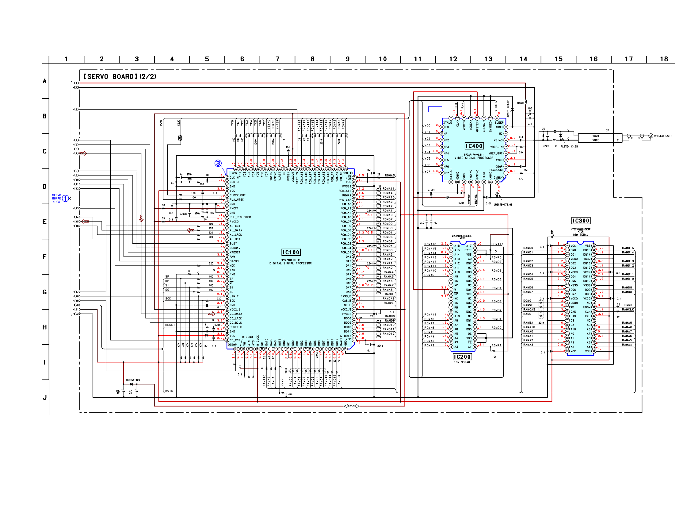
3-7. SCHEMATIC DIAGRAM — CD MECHANISM SECTION (2/2) — • Refer to page 26 for IC Block Diagram. • Refer to page 29 for IC Pin Description of IC400.
IC B/D
RB110
TP131
C132
R105
R104
R103
RB109
RB108
IC400
BP7
R108
R107
R106
RB111
D909
L401
C404
R402
C401
C402
R403
C405
FB503
FB504
TP401
TP402
D906
CN401
CDX-V3800
CN401
(Page 18)
C102
C103
D101
R163
R165
C406
C161
C164
C407
C163
R167
R161
R162
R169
X401
R629
R171
R405
C166
R164
TP189
R173
R175
R701
R703
R702
R704
R178
R166
R168
R170
R172
R177
R404
TP188
R180
C181
C160
C180
C162
R176
C165
C182
TP181
C183
TP182
TP183
TP184
TP185
R109
R110
R111
TP186
IC100
TP187
RB112
R181
RB113
R112
R113
R114
RB106
RB105
RB104
RB103
RB102
R101
C131
C111
R102
RB107
RB101
C112
C201
C400
C202
FB502
C133
IC200
C410
R630
R631
D907
C403
R401
C302
C303
C304
RB301
C305
C301
IC300
C313
C312
R312
R311
CDX-V3800
19 19
Page 20
CDX-V3800
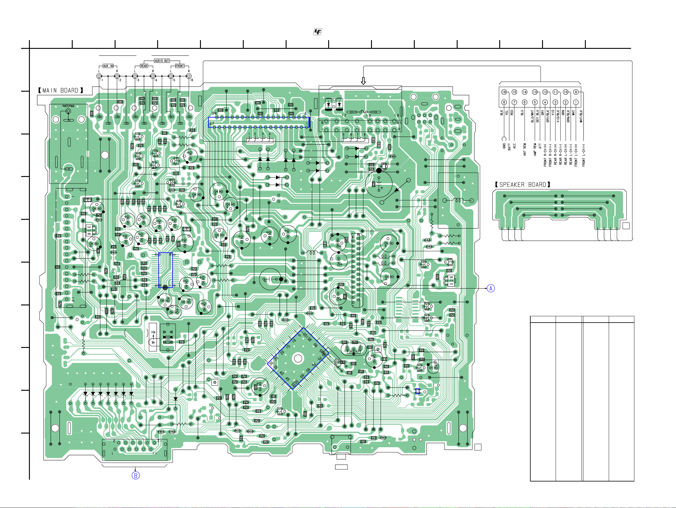
3-8. PRINTED WIRING BOARDS — MAIN SECTION — • Refer to page 15 for Circuit Boards Location. : Uses unleaded solder.
A
B
C
D
E
F
G
H
I
J
CDX-V3800
1
C612
R608
4
JW
R606
R607
JW47
JW48
3
JW
PJ601
TUX601
234567891011 12 13 14
PJ401
C991
117
JW
JW
C993
IC100
C821
R850
R849
116
JW
141
JW
JW65
R839
R830
R817
115
JW
R826
112
JW
JW111
D904
C810
R840
C807
R816
R427
D905
114
JW
C813
C809
R841
Q800
D922
D921
68
JW
D702
C994
140
JW
D907
C109
69
JW
25
JW
C990
JW143
JW106
D906
JW72
JW76
JW74
JW73
JW70
IC801
C706
24
JW
JW109
L700
R843
D701
110
JW
JW108
JW107
105
JW
22
JW
D902
D908
D909
104
JW
L703
R705
R916
C707
JW75
20
JW
91
JW
X801
C711
C701
R708
JW10
R846
RESET
2020
R853
R854
S802
S802
C816
19
JW
D903
D916
D917
FB702
C709
R836
R847
R936
X800
C817
JW18
CNP901
JW103
R837
C812
R873
17
JW
C815
F901
R932
102
JW
R709
142
JW
R814
R931
101
JW
CN751
JW82
JR12
C822
C992
L702
JW49
R703
15
JW
R437
FB901
L701
FMB3
R848
R860
D918
C825
14
JW
D808
FB902
JW92
C704
C705
R810
JR5
R901
13
JW
D914
JW99
JW100
C922
R835
R845
R913
D919
11
JW
R925
JW12
JW98
R903
JW85
JW83
JW94
JW93
Q907
IC802
D912
Q902
JW79
R904
R902
Q900
D915
Q906
JW97
JW96
JW95
R917
JW77
JW84
JW78
R702
R701
JW80
JW8
C908
R928
R912
JW9
1-865-780-
L900
Q703
JW86
R824
R825
2
JW
Q701
1
JW
11
2
1
SERVO
BOARD
CN1
(Page 17)
200
JW
203
JW
204
JW
207
JW
4
3
• Semiconductor Location
Ref. No. Location
D301 E-2
D400 D-4
D600 E-2
D701 G-7
D702 G-6
D801 I-6
D802 I-5
D808 J-9
D811 I-3
D812 I-3
D813 I-3
D814 I-2
D815 I-2
D816 I-2
D817 I-2
D820 I-4
D823 J-4
D825 J-4
D902 B-7
D903 B-8
D904 C-6
D905 C-6
D906 C-7
D907 C-7
D908 C-7
D909 C-7
D912 E-10
D914 C-9
D915 E-10
R615
61
JW
JW60
JW59
R604
R603
JW150
R815
L602
Q601
JW58
C443
JR10
D817
D600
C619
JW145
D815
6
JW
C618
C620
C451
C614
R430
R468
C409
50
JW
D816
C303
D301
51
JW
5
JW
C450
R426
R425
C408
D814
C439
C444
JW134
R415
JW144
R428
52
JW
D813
C436
R443
Q407
R420
R441
Q404
Q406
JW128
Q403
R440
R414
C423
C420
C426
R436
C453
R302
55
54
JW
JW
S800
FREQUENCY
SELECT
D812
D811
CNP800
DISPLAY BOARD
CN901
C435
Q405
JW131
C421
R416
C425
C452
R435
R413
R408
R409
R411
R412
56
JW
43
JW
JW44
(Page 24)
R442
C440
R419
JW127
JW130
C422
R404
C412
42
JW
D823
R406
S800
41
JW
C434
R421
JR6
D400
C424
R405
IC401
D825
C438
Q402
R417
C454
JW39
Q401
Q400
R407
C433
R418
R431
R429
R424
C428
C416
C411
R800
R833
JW121
L400
R402
R403
C413
D820
C437
R432
C430
46
JW
C106
JW120
JW151
C417
34
JW
45
JW
40
JW
28
JW
JW122
R447
C447
C410
JW123
C446
C441
JW66
37
JW
FMB4
R809
C113
C101
R400
JW63
C414
JW126
JW125
JW124
R448
R401
JW67
JW62
36
JW
R832
R834
27
JW
C107
38
JW
D802
119
JW
35
JW
R806
30
JW
C111
R821
JW31
R812
R828
R823
R818
R801
R805
R804
29
JW
113
JW
118
JW
R927
R813
R822
D801
64
R819
201
JW
202
JW
205
JW
206
JW
5
Ref. No. Location
D916 C-8
D917 C-8
D918 C-9
D919 D-9
D921 D-6
D922 C-6
IC100 B-6
IC401 F-4
IC801 H-7
IC802 H-10
Q400 D-4
Q401 D-4
Q402 C-4
Q403 D-3
Q404 C-3
Q405 C-3
Q406 C-3
Q407 C-3
Q601 E-2
Q701 F-10
Q703 F-10
Q800 I-6
Q900 H-10
Q902 F-10
Q906 G-10
Q907 G-10
1-865-781-
7
6
8
11
Page 21
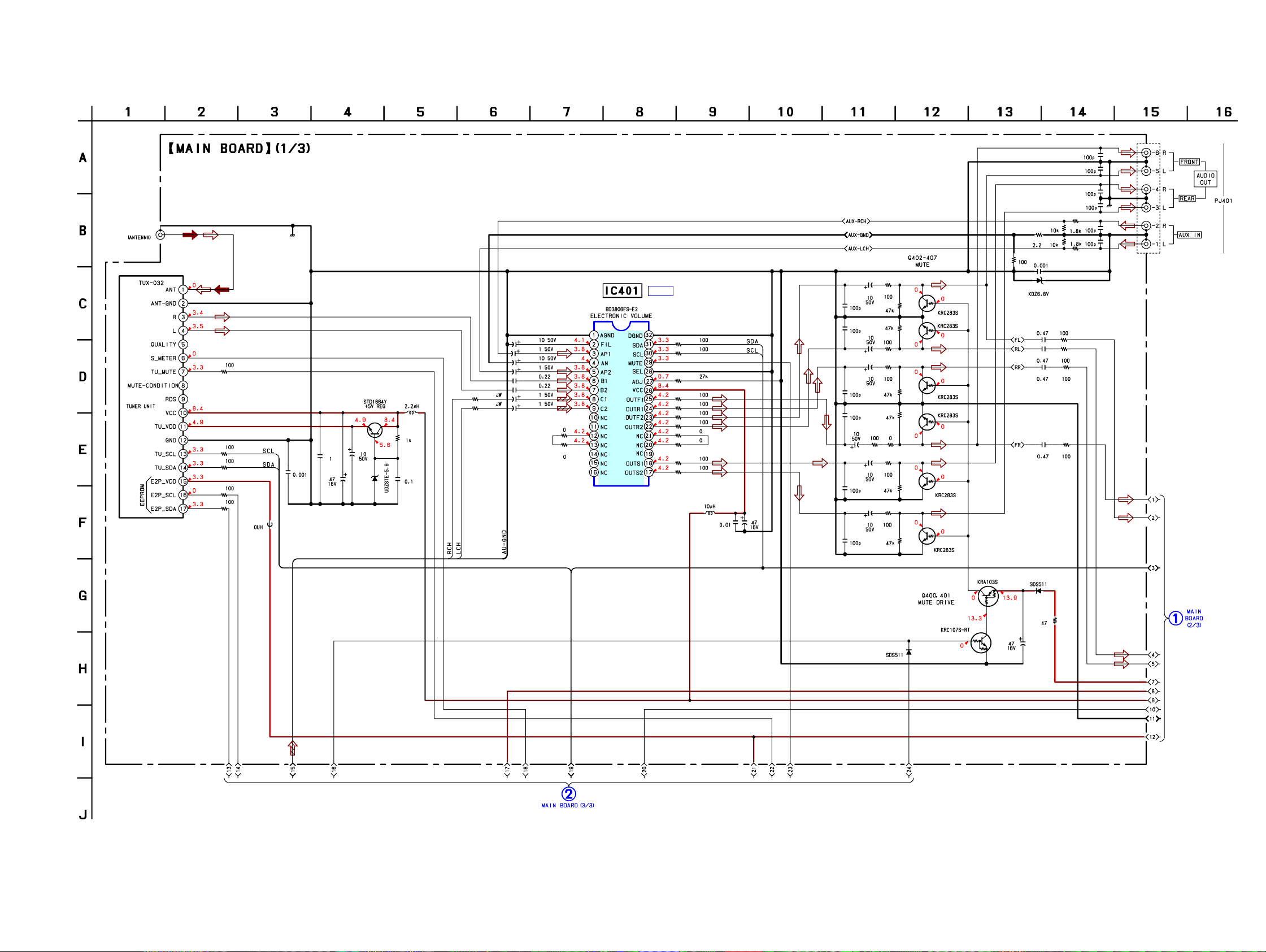
3-9. SCHEMATIC DIAGRAM — MAIN SECTION (1/3) — • Refer to page 26 for IC Block Diagram.
CDX-V3800
C433
C434
C435
C436
PJ601
TUX601
R606
R604
R603
R608
R607
JR10
C612
C614
C618
C619
Q601
D600
R615
C620
L602
R401
R400
C414
C413
C454
C412
C409
C408
C411
C410
R403
R402
IC401
IC B/D
R412
R411
R409
R407
R406
R405
R404
R408
R413
R435
R436
L400
C416
C417
C421
C420
C423
C422
C450
C451 R443
C428
C426
C425
C452
C453
R417
R421
R420
R415
R414
R419
R418
JR6
R440
R442
R441
R416
C424
Q406
Q407
Q405
Q404
Q403
Q402
R302
R425
R428
R468
C303
D301
C440 R431
C444
C438
C437 R427
R432
R429
R426
R430
C439
C443
(Page 23)
D702
Q400
Q401
C430
D400
R424
(Page 22)
CDX-V3800
21 21
Page 22

CDX-V3800
3-10. SCHEMATIC DIAGRAM — MAIN SECTION (2/3) —
C113
C101
(Page 21)
C993
C994
C107
C991
C990
IC100
C106
C111
C109
D921
D922
D904
D903
D902
D905
D906
D907
D908
D909
D917
D916
FB901
FB902
R931
R932
R913
D914
D918
C922
CNP901
F901
L900
C992
D919
CDX-V3800
C446 R447
C441
R448
C447
(Page 23)
Q900
R903
C908
R902 R904
R825
C706
Q906
R824
Q907
Q902
D915
D912
R928
R917
R912
2222
Page 23

• Refer to page 16 for Waveforms.
3-11. SCHEMATIC DIAGRAM — MAIN SECTION (3/3) — • Refer to page 30 for IC Pin Description of IC801.
CDX-V3800
(Page 18)
CN751
R843
C709
R708
R709
R703
C707
C701
FB702
D701
C704
C705
L700
L701
L702
C711
L703
R813
D820
R702
Q701
R701
Q703
R815
C807 R826
S800
R805
R806
R800
R809
(Page 21)
R834 R832
C813
C821
R801
R804
R819
R818
R828
R830
R821
R823
R822
C810
C809
R839
R840
R841
IC801
R705
JR12
R837
TP11
R836
R936
R853
C822
X800
(Page 22)
R901
R925
R846
R847
R810
C825
JR5
(Page 25)
CNP800
D825
D817
D815
D816
D814
D813
D812
D811
D823
R833
D802
R814
R850
D801
R849
Q800
R812
R835
R927
R817
R916
R816
R848
R873
R854
X801
C816 C817
C812
C815
R845
R860
D808
IC802
R437
S802
CDX-V3800
23 23
Page 24
CDX-V3800
3-12. PRINTED WIRING BOARD — DISPLAY SECTION — • Refer to page 15 for Circuit Boards Location. : Uses unleaded solder.
A
B
C
D
1
LED507,
S509
ATT
LED521,
S507
(VOLUME)
LED520,
S508
234567891011 12 13 14
LED507
LED521
S507
S522 (OPEN)
LED520
S508
EJECT
LED513,S516
DSPL
LED501
(LCD BACK LIGHT)
S516
LED513
LED501
LED524
S502 LED524,S504 LED525,S505
SOURCE
ODE
M
LED503
(CD WINDOW)
LED510
LCD501
5/OSD
LED509
6/PAUSE
LED508
SENS/–
LED506
ALBUM
BTM
LED518
/+
(LCD BACK LIGHT)
LIQUID CRYSTAL DISPLAY PANEL
2/SHUF
LED504
3/SLOW
LED511
4/AUDIO
LED525
LED522,S506 LED505,S511 LED504,S512 LED511,S521 LED510,S520 LED509,S519 LED508,S518 LED506,S510 LED518,S523 LED512,S517
LED522
SEL
LED505
1/REP
LED514,S515
EQ3
S515
LED502
LED514
LED502
SCRL
LED512
S513
S514
S501 IC502
EJECT
LED517
LED516
LED515
S503
IC502
3
2
1-865-782-
LED515,
S503
OFF
LED517,
S513
SEEK
LED516,
S514
4
1
11
E
F
G
H
R580
R507
R506
R505
R508
R578
R513
R533
R532
R531
R579
R504
R509
R577
R510
R576
FM
MAIN BOARD CNP800
(Page 20)
B
R503
R518
IC501
R536
R537
B3
R517
R555
R516
R575
R519
R554
FM
B4
R557
R553
R574
R515
R514
C553
C960
D551
R561
D552
Q502
R535
212
CN901
111
D503
D505
R552
R558
D504
R573
R560
R502
R512
D502
R559
R511
R501
R572
R551
1-865-782-
C551
R571
11
CDX-V3800
• Semiconductor Location
Ref. No. Location
D502 F-13
D503 G-11
D504 F-13
D505 G-12
D551 H-10
D552 G-10
IC501 G-7
IC502 D-14
Ref. No. Location
LED501 C-4
LED502 C-12
LED503 B-7
LED504 D-6
LED505 D-6
LED506 D-11
LED507 A-2
LED508 D-10
LED509 D-9
Ref. No. Location
LED510 D-8
LED511 D-7
LED512 D-12
LED513 C-3
LED514 C-12
LED515 A-14
LED516 C-14
LED517 B-13
LED518 D-11
Ref. No. Location
LED520 D-2
LED521 B-2
LED522 D-5
LED524 D-3
LED525 D-4
Q502 G-10
2424
Page 25
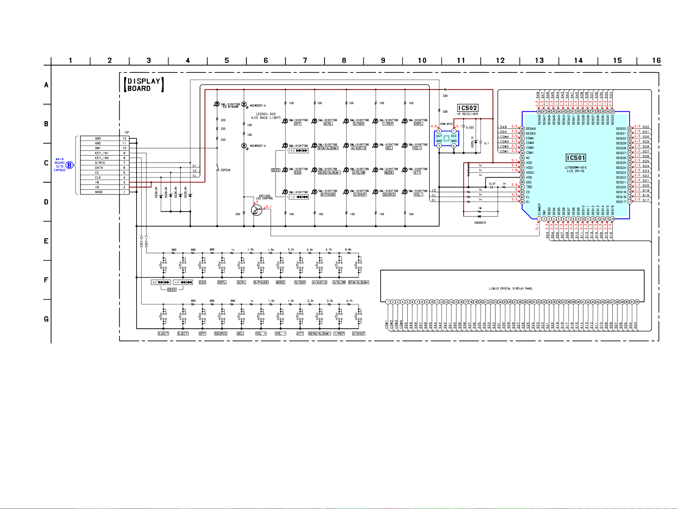
3-13. SCHEMATIC DIAGRAM — DISPLAY SECTION —
CN901
R533
R532
R531
LED503
R537
R536
LED501
LED502
R571 R573 R575 R577 R579
LED515
LED517
LED512 LED509
LED518
LED510
LED505
LED522
LED513
LED521
R552
R551
IC502
C551
D551
CDX-V3800
C960
(Page 23)
D502
D503
D504
R511 R512
S522
Q502
D505
R513
R501 R502 R504 R505 R506 R507 R508 R509 R510
R514
S517S514 S519 S520S515 S521S516 S518 S505 S523S513
R535
R515
R503
S508 S509S504 S506 S507S503S502 S511S510 S512S501
LED514
LED516
R572 R574 R576 R578 R580
R516
R517
LED506
LED508
R518 R519
LED511
LED504
LED525
LED524
LED507
LED520
R553
R554
R555
R558
R559
R560
IC501
C553 R557
R561
D552
LCD501
CDX-V3800
25 25
Page 26

CDX-V3800
• IC BLOCK DIAGRAMS
IC500 BU9536KS2 (SERVO Board (1/2))
EQO
RFI
CAGC
TEN
TEOSCTZCRFM
RFRPRFN
DIGITAL
SERVO
FILTER
DIGITAL SERVO
SIGNAL
PROCESSOR
17 18 19 20 21 22 26252423
SDIN
FDOUT
TDOUT
SDOUT
JUMPO
AVDD
VBIAS
AGND
FEN
FEO
PKC
BTC
51 5052
49 48 47 46 45 44 43 42 41 40
1
AC
2
BD
3
4
E
5
F
6
7
8
9
10
11
PD
12
LD
13
RF SIGNAL GEN.
GEN.
SERVO SIGNAL
APC
PLL
14 15 16
FCO
PCO
ASY
DGNDXOXI
CLK88
CLVOUT
DIGITAL
SIGNAL
PROCESSOR
16K
SRAM
COMMAND
INTERFACE
CLK
LON
MCK
DVDD
XPLCK
39
38
37
36
35
34
33
32
31
30
29
28
27
XBUFO
EFLAG
DCK
LRCK
DOUTA
WFCK
SUBCK
SUBDATA
SUBSYQ
BUSY
RESETX
R/W
DIO
IC700 WM8726GED/R (SERVO Board (1/2)) IC400 SPCA717A-HL211 (SERVO Board (2/2))
LRCIN
DIN
BCKIN
CAP
VOUTR
GND
1
2
3
NC
4
5
SIGMA-DELTA
MODULATOR
6
7
DIGITAL
SWICHED
CAPACITOR
DAC
SERIAL
INTERFACE
DIGITAL
FILTER
DIGITAL
SIGMA-DELTA
MODULATOR
SWICHED
CAPACITOR
DAC
14
13
12
11
10
9
8
SCKI
FORMAT
DEEMPH
NC
MUTE
VOUTL
VDD
FSADJUST
COMP
VAA
VREFOUT
VREFIN
VBIAS
AGND
1
2
3
4
5
6
7
8
9
DAC
INTERNAL
VREF
VBI
GENERATOR
9
SLEEP
CVBS/Y32AGND31TEST30HSYNC29VSYNC28VDD27DGND26CLKOUT
LATCH
1.3MHz
LPF
2X
UPSAMPLE
MOD.AND
MIXER
10
11
12
14
15
16
MODEA13MODEB
MASTER
CLK
XTALO
LUMA
CBSWP
25
24
23
22
21
20
19
18
17
IC401 BD3806FS-E2 (MAIN Board (1/3))
DGND
SDA
SCL
MUTE
SEL
ADJ
VCC
OUTF1
OUTR1
OUTF2
OUTR2
NC
NC
NC
OUTS1
32 31 30 29 28 27 26 25 24 23 22
21 20 19 18 17
OUTS2
DATA7
DATA6
DATA5
DATA4
DATA3
DATA2
DATA1
DATA0
IC600 BA5966FP-FE2 (SERVO Board (1/2))
REV
OPIN4(+)
OPIN4(–)
OPOUT4
OPIN3(+)
OPIN3(–)
2728 26 25
+–
LOADING DRIVER
REV
OUT F
FWD
OUT R
24 23 22 21 20 19 18 17 16 15
+–
–
+
+
–
OPOUT3
VCC
2
I
C BUS
LOGIC
BASS
fo:60,70,80,100,120,140,160,200Hz
Q:0.5,0.75,1,1.25
MIDDLE
fo:500Hz,1kHz
MUTE
BIAS
GND
VO3(–)
VO3(+)
MUTE
+–
+–
+
–
+
+
–
–
LEVEL
SHIFT
LEVEL
SHIFT
–+
VO4(–)
+–
–
LEVEL
SHIFT
LEVEL
SHIFT
–
VO4(+)
+–
+
+
Q:1
TABLE
fo:5,7.5,10,12.5kHz
VCO
FADER
(0~-58,
-∞dB)
EFFECT (0dB~
+20dB,2dB STEP)
TONE
PASS
fc:40kHz fc:40kHz
(0~15dB,1dB STEP)
(4 STEREO INCLUDE 1 ISOLATION INPUT)
FADER
(0~-58,
-∞dB)
BASS,TREBLE, MIDDLE
(-15dB~+15dB,1dB STEP)
VOLUME
(+23~-79dB,-∞dB
1dB STEP)
ANTI-ALIASING
FILTER
INPUT GAIN
MUTE
INPUT SELECTOR
FADER
(0~-58,
-∞dB)
EFFECT (0dB~
+20dB,2dB STEP)
TONE
PASS
BASS,TREBLE, MIDDLE
(-15dB~+15dB,1dB STEP)
(+23~-79dB,-∞dB
ANTI-ALIASING
(0~15dB,1dB STEP)
(0~-58,
VOLUME
1dB STEP)
FILTER
INPUT GAIN
MUTE
FADER
-∞dB)
2ND ORDER LPF
fc:OFF,80,120,160Hz
Q: 0.707
MIX
GAIN+ATT
(+10~-29,
-∞dB)
2ND ORDER
LPF
FWD
CDX-V3800
+–+–
4 5 6 7 8 9 10 11 12 13 1421 3
OPIN1(–)
OPOUT1
OPIN1(+)
OPIN2(+)
OPIN2(–)
OPOUT2
VCC
VCC
VOL(–)
VOL(+)
+–
VO2(–)
+–
VO2(+)
+–
VO1(–)
+–
VO1(+)
VCC/2
AGND
6 7 8 9 10 113 4 521
AP1
AN
FIL
AP2
B1
B2
C2
C1
NC
NC
12 14 1613 15
NC
NCNCNC
NC
2626
Page 27

• IC PIN DESCRIPTIONS
• IC500 BU9536KS2 (RF AMP, DIGITAL SERVO) (SERVO BOARD (1/2))
Pin No. Pin Name I/O Pin Description
1AVDD1 — Analog power supply pin (+3.3 V)
2ACIA+C voltage signal input from optical pick-up block
3BDIB+D voltage signal input from optical pick-up block
4VBIAS O Bias level (VDD/2) signal output
5EIE voltage signal input from optical pick-up block
6FIF voltage signal input from optical pick-up block
7AGND1 — Analog ground pin
8 FEN I Focus error amplifier feedback signal input
9 FEO O Focus error signal output
10 PKC O RF signal peak detection capacitance connected pin
11 BTC O RF signal bottom detection capacitance connected pin
12 PD I APC photo detecter signal input
13 LD O APC laser drive signal output
14 PCO O PLL PCO signal output
15 FCO O PLL FCO-DAC signal output
16 ASY I Asymmetry revice and ccomparator slice capacitor install pin
17 JUMPO O Tracking jump pulse signal output
18 TDOUT O Tracking drive signal output
19 SDIN I Sled signal input
20 SDOUT O Sled drive signal output
21 FDOUT O Focus drive signal output
22 CLVOUT O CLV drive signal output
23 CLK88 O Clock signal output for driver IC Not used in this set. (Open)
24 LON O Laser on control signal output
25 CLK O Clock signal output Not used in this set. (Open)
26 MCK I Transfer clock signal input for sub Q and command
27 DIN/DOUT I/O Command signal input/status, sub-Q signal output
28 R/W I Read/write signal input for command
29 RESETX I System reset signal input “L”: reset
30 BUSY O Busy signal output
31 SUBSYQ O Sub cord synchronizing signal output
32 SUBDATA O Sub cord data signal output
33 SUBCK I Sub cord bit clock signal input Not used in this set. (Fixed at “L”.)
34 WFCK O Disc frame synchronizing signal output
35 DOUTA O Audio serial data signal output
36 LRCK O Audio LR signal output
37 DCK O Audio serial bit clock signal output
38 EFLAG I/O Error flag signal input/output
39 BUFO O X'tal 16.9344 MHz buffer signal output Not used in this set. (Open)
40 XPLCK I/O XPLCK signal input/output Not used in this set. (Open)
41 DVDD — Digital power supply pin (+3.3 V)
42 XI I X'tal 16.9344 MHz connect input
43 XO O X'tal 16.9344 MHz connect output
44 DGND — Digital ground pin
45 RFRPPFM O RFRP capacitor install pin or RF test monitor signal output
46 TZCRFM O TZC capacitor install pin or RF monitor signal output
47 SC I Scratch depth adjustment resistor connected pin
48 TEO O Tracking error signal output
CDX-V3800
27
Page 28

CDX-V3800
Pin No. Pin Name I/O Pin Description
49 TEN I Tracking error amplifier feedback signal input
50 CAGC I RFAGC capacitor install pin
51 RFI I RF signal input
52 EQO O RF equalizer signal output
28
Page 29

CDX-V3800
• IC400 SPCA717A-HL211 (VIDEO SIGNAL PROCESSOR) (SERVO BOARD (2/2))
Pin No. Pin Name I/O Pin Description
1 FSADJUST —
2 COMP —
3AVCC — Analog power supply pin (+3.3 V)
4 VREF OUT O
5 VREF IN I
6VBIAS — DAC bias voltage Potential normally 0.7 V less than pin 2 (COMP).
7NC—Not used. (Open)
8AGND — Analog ground pin
9 SLEEP I pin is equal to reset pin. An external logic high pulse should input to the pin when
10 SVIDEO I
11 CBSWAP I
12 MASTER I
13 MODEA I Mode configuration pin Not used in this set. (Fixed at “L”.)
14 MODEB I Mode configuration pin
15 CLK I
16 XTALO O Crystal oscillator output Not used in this set. (Open)
17 to 24 P0 to P7 I
25 CLKOUT O Pixel clock signal output Not used in this set. (Open)
26 DGND — Digital ground pin
27 VDD — Digital power supply pin (+3.3 V)
28 VSYNC I/O
29 HSYNC I/O
30 TEST I Test pin These pins must be connected to digital ground.
31 AGND — Analog ground pin.
32 CVBSY O
Full-Scale adjust control pin The Full-Scale current of D/A converters can be
adjusted by connecting a resistor (RESET) between this pin and ground.
Compensation pin A0.1 µF ceramic capacitor must be used to bypass this pin to VAA.
The lead length must be kept as short as possible to avoid noise.
Voltage reference signal output It generates typical 1.2 V voltage reference and may
be used to drive pin 5 (VREF IN) directly.
Voltage reference signal input An external voltage reference must supply typical
1.235 V to this pin. A0.1 µF ceramic capacitor must be used to de-couple this input
to ground. The decoupling capacitor must be as closed as possible to minimize the
length of the load. The pin may be connected derectry to pin 4 (VREF OUT).
Power save mode A logic high on this pin puts the chip into power-down mode. This
power on.
Video signal selection pin A logic high selects Y output. A logic low selects
composite video output. Not used in this set. (Fixed at “L”.)
Cr and Cb pixel sequence configuration pin A logic high sw ap the Cr and Cb sequence.
Not used in this set. (Fixed at “L”.)
Master/Slave mode selection A logical high for master mode operation. A logical 0
for slave mode operation. Not used in this set. (+3.3 V)
27 MHz crystal oscillator input A crystal with 27 MHz clock frequency can be
connected between this pin and pin qh (XTALO).
YCrCb pixel inputs
They are latched on the rising edge of CLK.
Vertical sync input/output
VSYNC is latched/output following the rising edge of CLK.
Horizontal sync input/output
HSYNC is latched/output following the rising edge of CLK.
Composite/Luminance output. This is a high-impedance current source output. The
output format can be selected by the PAL pin. The CVBSY can drive a 37.5 Ω load.
29
Page 30

CDX-V3800
• IC801 MB90488BPF-G-135-BNDE1 (SYSTEM CONTROL) (MAIN BOARD (3/3))
Pin No. Pin Name I/O Pin Description
1 LINE ATT O Audio mute control signal output
2 to 4 NC — Not used in this set. (Open)
5 BEEP O Beep signal output to power amp IC
6VOL ATT O Electrical volume ATT control signal output
7 to 10 NC — Not used in this set. (Open)
11 VSS — Ground pin
12 to 14 NC — Not used in this set. (Open)
15 TU ATT O Tuner mute control signal output
16, 17 NC — Not used in this set. (Open)
18 CD SI I CD servo serial data signal input
19 CD SO O CD servo serial data signal output
20 CD SCK O CD servo serial clock signal output
21, 22 NC — Not used in this set. (Open)
23 VCC+3.3 — Power supply pin (+3.3 V)
24 EEP SIO I/O Serial data signal input/output for EEPROM communication
25 EEP SCK O Serial clock signal output for EEPROM communication
26 SHUT SW I
27 LCD CE O Chip enable signal output to LCD driver IC
28 LCD SO O Serial data signal output to LCD driver IC Flash: UART serial out
29 LCD SCK O Serial clock signal output to LCD driver IC
30 NC — Not used in this set. (Open)
31 STB O Standby signal output to power amp IC
32 AUX — Not used in this set. (Open)
33 IIC SCK O IIC bus serial clock signal output
34 IIC SIO I/O IIC bus serial data signal input/output
35 VCC+3.3 — Power supply pin (+3.3 V) (for A/D converter)
36 AVRH+3.3 — External reference power supply (+3.3 V) (for A/D converter)
37 AVSS — Ground pin (for A/D converter)
38, 39 KEY IN0, 1 I Key signal input
40 NC — Not used in this set. (Open)
41 NC — Not used in this set. (Fixed at “H”.)
42 VSS — Ground pin
43, 44 NC — Not used in this set. (Fixed at “L”.)
45 VSM I S meter voltage detect signal input
46 DST SEL I Destination select pin
47 KEY ACK I Key acknowledge detect signal input
48 NC — Not used in this set. (Open)
49, 50 MD0, 1 I Input for operation mode designation (Fixed at “H”.)
51 MD2 I Input for operation mode designation (Fixed at “L”.)
52 NC — Not used in this set. (Open)
53 BU IN I Back up power supply detect signal input
54 SP O SP mode select signal output
55 CD SELFSW I CD mechanism self load position detect switch signal input
56 DIAG I Condition input from power amp IC
57 NC — Not used in this set. (Open)
58 UNI SI I Serial data signal input
59 UNI SO O Serial data signal output
60 UNI SCK O Serial clock signal output Not used in this set. (Open)
61 BUS ON O Bus on signal output
62 SYS RST O System reset signal output
63 NC — Not used in this set. (Open)
Shutter switch open/close detect signal input
“L”: Panel open, “H”: Panel close Not used in this set. (Open)
30
Page 31
CDX-V3800
Pin No. Pin Name I/O Pin Description
64 ACC IN I Accessory power supply detect signal input
65 SIRCS I Remote control signal (infrared rays) input
66 NC — Not used in this set. (Fixed at “L”.)
67 PAK BK I Test mode detect signal input
68 FLASH W I
69 to 71 NC — Not used in this set. (Open)
72 DOOR SW I
73, 74 NC — Not used in this set. (Fixed at “H”.)
75 XKEY ON O Key power supply control signal output Pin rj (KEY ACK) active: “L” output
76 NC — Not used in this set. (Open)
77 RESET I Reset signal input
78 NC — Not used in this set. (Open)
79 X1A — Oscillator connect pin (32.768 kHz)
80 X0A — Oscillator connect pin (32.768 kHz)
81 VSS — Ground pin
82 X0 — Oscillator connect pin (3.68 MHz)
83 X1 — Oscillator connect pin (3.68 MHz)
84 VCC+3.3 — Power supply pin (+3.3 V)
85, 86 NC — Not used in this set. (Open)
87 CD ON O CD power on/off control signal output
88 NC — Not used in this set. (Open)
89 TEST MODE I Test mode pin
90 MP O MP mode select signal output
91 NC — Not used in this set. (Open)
92 CD IN SW I CD mechanism IN-SW detect signal input
93 CD LOAD O CD mechanism loading motor control signal output
94 EJECT O CD mechanism eject motor control signal output
95 D SW I CD mechanism DSW detect signal input
69, 97 NC — Not used in this set. (Open)
98 CD XRST O CD servo reset signal output
99 NC — Not used in this set. (Open)
100 NC — Not used in this set. (Open)
Memory mode changeover signal input
Normally “H” input (single chip mode) “L” after reset: Flash write mode
Front panel open/close detect signal input
“L” input: Panel close, “H” input: Panel open
31
Page 32
CDX-V3800
2
NOTE:
• The mechanical parts with no reference
number in the exploded views are not supplied.
• Items marked “*” are not stocked since
they are seldom required for routine service.
Some delay should be anticipated
when ordering these items.
• -XX and -X mean standardized parts, so
they may have some difference from the
original one.
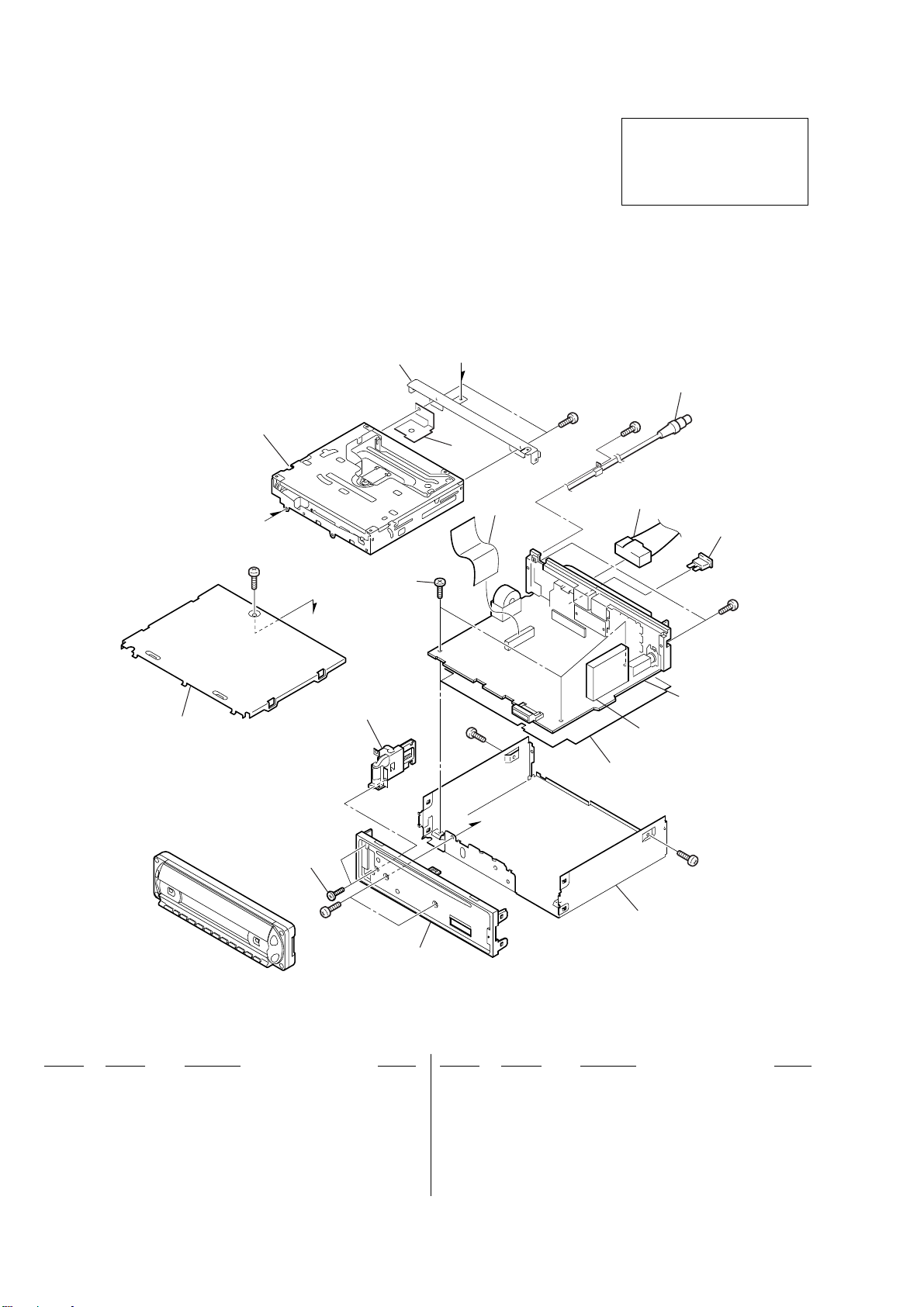
4-1. MAIN SECTION
SECTION 4
EXPLODED VIEWS
• Color Indication of Appearance Parts
Example :
KNOB, BALANCE (WHITE) ... (RED)
RR
Parts Color Cabinet’s Color
• Accessories are given in the last of this
parts list.
The components identified by
mark 0 or dotted line with mark
0 are critical for safety.
Replace only with part number
specified.
MG-611MM-186//K
4
#1
B
A
not supplied
5
3
10
#1
A
9
#1
6
#2
8
F901
#
7
TUX601
not supplied
2
#1
Ref. No. Part No. Description Remark
1 X-3384-407-1 PANEL (1) ASSY, SUB
2 3-231-472-02 SCREW (+B 2X4)
3 X-3382-588-1 LOCK ASSY (S)
* 4 3-246-006-31 COVER
5 3-922-535-11 SCREW (+BTT)
6 1-829-847-11 CABLE, FLAT (FFC) 26P
7 A-1096-245-A MAIN BOARD, COMPLETE
B
#1
not supplied
1
Ref. No. Part No. Description Remark
8 1-792-194-61 CORD (WITH CONNECTOR) (POWER)
9 1-829-836-12 CORD, CONNECTION (VIDEO OUT)
10 2-178-708-01 SHEET, SHIELD
F901 1-532-877-11 FUSE (BLADE TYPE) (AUTO FUSE) 10A
TUX601 A-3220-961-A TUNER UNIT (TUX-032)
#1 7-685-792-09 SCREW +PTT 2.6X6 (S)
#2 7-685-793-09 SCREW +PTT 2.6X8 (S)
32
Page 33
4-2. FRONT PANEL SECTION
CDX-V3800
LCD501
not supplied
not supplied
61
not supplied
(DISPLAY board)
not supplied
57
64
58
53
63
59
#3
55
not supplied
60
#3
56 65
not
supplied
not supplied
not supplied
54
51 X-2024-914-1 PANEL (BASE) ASSY, FRONT
52 3-258-879-01 FILTER (IR)
53 1-780-120-11 CONDUCTIVE BOARD, CONNECTION
54 X-3384-622-1 SHUTTER ASSY
55 X-3384-457-2 BUTTON ASSY (S)
56 3-246-211-01 SPRING (RELEASE)
57 3-258-884-01 SHEET (ILLUMINATOR)
58 3-258-880-01 PLATE (CD), LIGHT GUIDE
59 3-258-869-02 PANEL, FRONT BACK
52
not supplied
51
62
Ref. No. Part No. Description RemarkRef. No. Part No. Description Remark
60 X-3378-390-3 CASE ASSY (for FRONT PANEL)
61 A-1096-248-A PANEL COMPLETED ASSY, FRONT
62 3-258-874-12 BUTTON (SEEK)
63 3-258-873-12 BUTTON (+.–)
64 X-3384-621-2 RETRACTABLE ASSY
65 3-258-875-31 BUTTON (PRESET)
LCD501 1-805-451-11 DISPLAY PANEL, LIQUID CRYSTAL
#3 7-685-105-19 SCREW +P 2X8 TYPE2 NON-SLIT
33
Page 34

CDX-V3800
4-3. CD MECHANISM SECTION (1)
(MG-611MM-186//K)
not supplied
not supplied
102
not supplied
(SENSOR board)
not supplied
101
#4
not supplied
103
104
106
105
107
#4
Ref. No. Part No. Description Remark Ref. No. Part No. Description Remark
101 A-3372-455-A CHASSIS (T) SUB ASSY
102 3-253-729-01 SPRING (LTR), TENSION COIL
103 3-253-746-14 SPRING (DAMPER), COMPRESSION
104 3-253-746-03 SPRING (DAMPER), COMPRESSION
105 2-345-767-01 SPRING (KF60), TENSION
106 3-253-748-01 DAMPER (S)
107 A-1107-620-A SERVO BOARD, COMPLETE
#4 7-627-552-87 SCREW, PRECISION +P 1.7X2.2
34
Page 35

4-4. CD MECHANISM SECTION (2)
(MG-611MM-186//K)
154
(including M901)
CDX-V3800
155
156
157
#5
SW4
151
not supplied
M902
not supplied
not supplied
158
153
not supplied
152
The components identified by
mark 0 or dotted line with mark
0 are critical for safety.
Replace only with part number
specified.
Ref. No. Part No. Description Remark Ref. No. Part No. Description Remark
151 A-1075-786-A CHASSIS (OP) COMPLETE ASSY
152 3-316-938-91 SCREW (B1.4X5), TAPPING
0 153 8-820-207-12 OPTICAL PICK-UP (KSS1000E/K1RP)
154 A-1075-787-A CHASSIS (OP) SUB ASSY (including M901)
155 A-3337-641-A ARM SUB ASSY, CHUCKING
156 A-3337-639-A LEVER (SL) SUB ASSY
157 X-3383-454-3 LEVER (SL) ASSY
158 3-261-959-02 SPRING (SL), TORSION
M902 A-3337-638-A MOTOR ASSY, SL (SLED)
SW4 1-571-099-11 SWITCH (1 KEY) (LIMIT)
#5 7-627-850-77 SCREW, PRECISION +P 1.4X1.8
35
Page 36

CDX-V3800
4-5. CD MECHANISM SECTION (3)
(MG-611MM-186//K)
209
207
208
201
202
207
#4
M903
206
207
210
203
211
204
205
Ref. No. Part No. Description Remark Ref. No. Part No. Description Remark
201 3-262-755-01 WASHER (1.1-2.5)
202 2-186-699-11 GEAR (RA1)
203 A-1075-789-A ARM ASSY, ROLLER
204 3-259-455-02 SPRING (RAL)
205 3-253-713-01 SPRING (RAR)
206 3-259-469-01 SPRING (LE), LEAF
207 2-134-636-31 SCREW (M1.7X2.5)
208 2-186-696-11 BRACKET (LEM-N)
209 3-345-648-91 SCREW (M1.4), TOOTHED LOCK
210 A-1083-637-A GEAR (LE) ASSY
211 2-186-697-11 BEARING (LEB-N)
M903 A-1075-792-A MOTOR ASSY, LE (LOADING)
#4 7-627-552-87 SCREW, PRECISION +P 1.7X2.2
36
Page 37

4-6. CD MECHANISM SECTION (4)
(MG-611MM-186//K)
252
CDX-V3800
254
252
255
251
256
253
257
Ref. No. Part No. Description Remark Ref. No. Part No. Description Remark
251 2-186-700-11 GEAR (CHK1)
252 3-344-223-01 WASHER
253 3-259-470-01 GEAR (LE1)
254 3-253-755-02 LEVER (D)
255 3-899-829-01 WASHER (SLIT)
256 3-259-032-01 GEAR (LE2)
257 A-1075-791-A CHASSIS (M) BLOCK ASSY
37
Page 38

CDX-V3800
SECTION 5
DISPLAY
NOTE:
• Due to standardization, replacements in
the parts list may be different from the
parts specified in the diagrams or the
components used on the set.
• -XX and -X mean standardized parts, so
they may have some difference from the
original one.
• RESISTORS
All resistors are in ohms.
METAL:Metal-film resistor.
METAL OXIDE: Metal oxide-film resistor.
F:nonflammable
Ref. No. Part No. Description Remark Ref. No. Part No. Description Remark
DISPLAY BOARD
**************
1-780-120-11 CONDUCTIVE BOARD, CONNECTION
3-258-884-01 SHEET (ILLUMINATOR)
ELECTRICAL PARTS LIST
• Items marked “*” are not stocked since
they are seldom required for routine service.
Some delay should be anticipated
when ordering these items.
• SEMICONDUCTORS
In each case, u : µ, for example:
uA.. : µA.. uPA.. : µPA..
uPB.. : µPB.. uPC.. : µPC.. uPD.. : µPD..
• CAPACITORS
uF : µF
• COILS
uH : µH
LED515 8-719-053-09 LED SML-310VTT86 (OFF)
LED516 8-719-053-09 LED SML-310VTT86 (SEEK –/m .)
LED517 8-719-053-09 LED SML-310VTT86 (SEEK +/> M)
LED518 8-719-053-09 LED SML-310VTT86 (BTM/ALBUM +)
LED520 8-719-053-09 LED SML-310VTT86 (VOL –)
The components identified by
mark 0 or dotted line with mark
0 are critical for safety.
Replace only with part number
specified.
When indicating parts by reference
number, please include the board.
< CAPACITOR >
C551 1-164-227-11 CERAMIC CHIP 0.022uF 10% 25V
C553 1-125-891-11 CERAMIC CHIP 0.47uF 10% 10V
C960 1-107-826-11 CERAMIC CHIP 0.1uF 10% 16V
< CONNECTOR >
CN901 1-794-312-21 PIN, CONNECTOR 12P
< DIODE >
D502 8-719-977-12 DIODE DTZ6.8B
D503 8-719-977-12 DIODE DTZ6.8B
D504 8-719-977-12 DIODE DTZ6.8B
D505 8-719-977-12 DIODE DTZ6.8B
D551 8-719-080-28 DIODE KDZ5.1V
D552 8-719-988-61 DIODE 1SS355TE-17
< IC >
IC501 6-707-063-01 IC LC75826WH-US-E
IC502 6-600-384-01 IC KSM-401E (IR)
< LIQUID CRYSTAL DISPLAY >
LCD501 1-805-451-11 DISPLAY PANEL, LIQUID CRYSTAL
LED521 8-719-053-09 LED SML-310VTT86 (VOL +)
LED522 8-719-053-09 LED SML-310VTT86 (SEL)
LED524 8-719-053-09 LED SML-310VTT86 (SOURCE)
LED525 8-719-053-09 LED SML-310VTT86 (MODE)
< TRANSISTOR >
Q502 8-729-038-67 TRANSISTOR KRC102S
< RESISTOR >
R501 1-216-819-11 METAL CHIP 680 5% 1/10W
R502 1-216-819-11 METAL CHIP 680 5% 1/10W
R503 1-216-823-11 METAL CHIP 1.5K 5% 1/10W
R504 1-216-819-11 METAL CHIP 680 5% 1/10W
R505 1-216-821-11 METAL CHIP 1K 5% 1/10W
R506 1-216-823-11 METAL CHIP 1.5K 5% 1/10W
R507 1-216-823-11 METAL CHIP 1.5K 5% 1/10W
R508 1-216-825-11 METAL CHIP 2.2K 5% 1/10W
R509 1-216-827-11 METAL CHIP 3.3K 5% 1/10W
R510 1-216-829-11 METAL CHIP 4.7K 5% 1/10W
R511 1-216-819-11 METAL CHIP 680 5% 1/10W
R512 1-216-819-11 METAL CHIP 680 5% 1/10W
R513 1-216-819-11 METAL CHIP 680 5% 1/10W
R514 1-216-821-11 METAL CHIP 1K 5% 1/10W
R515 1-216-823-11 METAL CHIP 1.5K 5% 1/10W
< DIODE >
LED501 6-500-459-01 LED NSCW505T-ARS (LCD BACK LIGHT)
LED502 6-500-459-01 LED NSCW505T-ARS (LCD BACK LIGHT)
LED503 8-719-053-09 LED SML-310VTT86 (CD WINDOW)
LED504 8-719-053-09 LED SML-310VTT86 (2/SHUF)
LED505 8-719-053-09 LED SML-310VTT86 (1/REP)
LED506 8-719-053-09 LED SML-310VTT86 (SENS/ALBUM –)
LED507 8-719-053-09 LED SML-310VTT86 (ATT)
LED508 8-719-053-09 LED SML-310VTT86 (6/PAUSE)
LED509 8-719-053-09 LED SML-310VTT86 (5/OSD)
LED510 8-719-053-09 LED SML-310VTT86 (4/AUDIO)
LED511 8-719-053-09 LED SML-310VTT86 (3/SLOW)
LED512 8-719-053-09 LED SML-310VTT86 (SCRL)
LED513 8-719-053-09 LED SML-310VTT86 (DSPL)
LED514 8-719-053-09 LED SML-310VTT86 (EQ3)
38
R516 1-216-825-11 METAL CHIP 2.2K 5% 1/10W
R517 1-216-827-11 METAL CHIP 3.3K 5% 1/10W
R518 1-216-829-11 METAL CHIP 4.7K 5% 1/10W
R519 1-218-867-11 METAL CHIP 6.8K 0.5% 1/10W
R531 1-216-813-11 METAL CHIP 220 5% 1/10W
R532 1-216-813-11 METAL CHIP 220 5% 1/10W
R533 1-216-813-11 METAL CHIP 220 5% 1/10W
R535 1-216-815-11 METAL CHIP 330 5% 1/10W
R536 1-216-809-11 METAL CHIP 100 5% 1/10W
R537 1-216-809-11 METAL CHIP 100 5% 1/10W
R551 1-216-815-11 METAL CHIP 330 5% 1/10W
R552 1-216-815-11 METAL CHIP 330 5% 1/10W
R553 1-216-821-11 METAL CHIP 1K 5% 1/10W
R554 1-216-821-11 METAL CHIP 1K 5% 1/10W
R555 1-216-821-11 METAL CHIP 1K 5% 1/10W
Page 39

CDX-V3800
DISPLAY MAIN
Ref. No. Part No. Description Remark Ref. No. Part No. Description Remark
R557 1-216-821-11 METAL CHIP 1K 5% 1/10W
R558 1-216-821-11 METAL CHIP 1K 5% 1/10W
R559 1-216-821-11 METAL CHIP 1K 5% 1/10W
R560 1-216-821-11 METAL CHIP 1K 5% 1/10W
R561 1-216-857-11 METAL CHIP 1M 5% 1/10W
C409 1-115-467-11 CERAMIC CHIP 0.22uF 10% 10V
C410 1-126-960-11 ELECT 1uF 20% 50V
C411 1-126-960-11 ELECT 1uF 20% 50V
C412 1-126-960-11 ELECT 1uF 20% 50V
C413 1-126-960-11 ELECT 1uF 20% 50V
R571 1-216-809-11 METAL CHIP 100 5% 1/10W
R572 1-216-809-11 METAL CHIP 100 5% 1/10W
R573 1-216-809-11 METAL CHIP 100 5% 1/10W
R574 1-216-809-11 METAL CHIP 100 5% 1/10W
R575 1-216-809-11 METAL CHIP 100 5% 1/10W
R576 1-216-809-11 METAL CHIP 100 5% 1/10W
R577 1-216-809-11 METAL CHIP 100 5% 1/10W
R578 1-216-809-11 METAL CHIP 100 5% 1/10W
R579 1-216-809-11 METAL CHIP 100 5% 1/10W
R580 1-216-809-11 METAL CHIP 100 5% 1/10W
< SWITCH >
S501 1-786-763-11 SWITCH, TACTILE (EJECT)
S502 1-786-763-11 SWITCH, TACTILE (EJECT)
S503 1-786-763-11 SWITCH, TACTILE (OFF)
S504 1-786-763-11 SWITCH, TACTILE (SOURCE)
S505 1-786-763-11 SWITCH, TACTILE (MODE)
S506 1-786-763-11 SWITCH, TACTILE (SEL)
S507 1-786-763-11 SWITCH, TACTILE (VOL +)
S508 1-786-763-11 SWITCH, TACTILE (VOL –)
S509 1-786-763-11 SWITCH, TACTILE (ATT)
S510 1-786-763-11 SWITCH, TACTILE (SENS/ALBUM –)
S511 1-786-763-11 SWITCH, TACTILE (1/REP)
S512 1-786-763-11 SWITCH, TACTILE (2/SHUF)
S513 1-786-763-11 SWITCH, TACTILE (SEEK +/> M)
S514 1-786-763-11 SWITCH, TACTILE (SEEK –/m .)
S515 1-786-763-11 SWITCH, TACTILE (EQ3)
S516 1-786-763-11 SWITCH, TACTILE (DSPL)
S517 1-786-763-11 SWITCH, TACTILE (SCRL)
S518 1-786-763-11 SWITCH, TACTILE (6/PAUSE)
S519 1-786-763-11 SWITCH, TACTILE (5/OSD)
S520 1-786-763-11 SWITCH, TACTILE (4/AUDIO)
S521 1-786-763-11 SWITCH, TACTILE (3/SLOW)
S522 1-529-566-61 SWITCH, PUSH (1 KEY) (OPEN)
S523 1-786-763-11 SWITCH, TACTILE (BTM/ALBUM +)
*************************************************************
A-1096-245-A MAIN BOARD, COMPLETE
(including SPEAKER BOARD)
*********************
7-621-284-40 SCREW +P 2.6X10
7-685-134-19 SCREW +P 2.6X8 TYPE2 NON-SLIT
7-685-793-09 SCREW +PTT 2.6X8 (S)
7-685-795-09 SCREW +PTT 2.6X12 (S)
< CAPACITOR >
C414 1-126-964-11 ELECT 10uF 20% 50V
C416 1-162-970-11 CERAMIC CHIP 0.01uF 10% 25V
C417 1-126-947-11 ELECT 47uF 20% 35V
C420 1-162-927-11 CERAMIC CHIP 100PF 5% 50V
C421 1-162-927-11 CERAMIC CHIP 100PF 5% 50V
C422 1-162-927-11 CERAMIC CHIP 100PF 5% 50V
C423 1-162-927-11 CERAMIC CHIP 100PF 5% 50V
C424 1-126-964-11 ELECT 10uF 20% 50V
C425 1-126-964-11 ELECT 10uF 20% 50V
C426 1-126-964-11 ELECT 10uF 20% 50V
C428 1-126-964-11 ELECT 10uF 20% 50V
C430 1-126-947-11 ELECT 47uF 20% 35V
C433 1-162-927-11 CERAMIC CHIP 100PF 5% 50V
C434 1-162-927-11 CERAMIC CHIP 100PF 5% 50V
C435 1-162-927-11 CERAMIC CHIP 100PF 5% 50V
C436 1-162-927-11 CERAMIC CHIP 100PF 5% 50V
C437 1-107-823-11 CERAMIC CHIP 0.47uF 10% 16V
C438 1-107-823-11 CERAMIC CHIP 0.47uF 10% 16V
C439 1-162-927-11 CERAMIC CHIP 100PF 5% 50V
C440 1-107-823-11 CERAMIC CHIP 0.47uF 10% 16V
C441 1-115-467-11 CERAMIC CHIP 0.22uF 10% 10V
C443 1-162-927-11 CERAMIC CHIP 100PF 5% 50V
C444 1-107-823-11 CERAMIC CHIP 0.47uF 10% 16V
C446 1-162-923-11 CERAMIC CHIP 47PF 5% 50V
C447 1-126-961-11 ELECT 2.2uF 20% 50V
C450 1-162-927-11 CERAMIC CHIP 100PF 5% 50V
C451 1-162-927-11 CERAMIC CHIP 100PF 5% 50V
C452 1-126-964-11 ELECT 10uF 20% 50V
C453 1-126-964-11 ELECT 10uF 20% 50V
C454 1-126-964-11 ELECT 10uF 20% 50V
C612 1-162-964-11 CERAMIC CHIP 0.001uF 10% 50V
C614 1-115-156-11 CERAMIC CHIP 1uF 10V
C618 1-126-947-11 ELECT 47uF 20% 35V
C619 1-126-964-11 ELECT 10uF 20% 50V
C620 1-107-826-11 CERAMIC CHIP 0.1uF 10% 16V
C701 1-124-584-00 ELECT 100uF 20% 10V
C704 1-124-584-00 ELECT 100uF 20% 10V
C705 1-124-584-00 ELECT 100uF 20% 10V
C706 1-162-964-11 CERAMIC CHIP 0.001uF 10% 50V
C707 1-124-584-00 ELECT 100uF 20% 10V
C709 1-162-964-11 CERAMIC CHIP 0.001uF 10% 50V
C711 1-124-589-11 ELECT 47uF 20% 16V
C807 1-162-970-11 CERAMIC CHIP 0.01uF 10% 25V
C809 1-104-665-11 ELECT 100uF 20% 25V
C810 1-125-701-11 DOUBLE LAYERS 0.047F 5.5V
C101 1-126-964-11 ELECT 10uF 20% 50V
C106 1-126-965-11 ELECT 22uF 20% 50V
C107 1-126-964-11 ELECT 10uF 20% 50V
C109 1-104-665-11 ELECT 100uF 20% 25V
C111 1-126-964-11 ELECT 10uF 20% 50V
C113 1-107-823-11 CERAMIC CHIP 0.47uF 10% 16V
C303 1-162-964-11 CERAMIC CHIP 0.001uF 10% 50V
C408 1-115-467-11 CERAMIC CHIP 0.22uF 10% 10V
C812 1-107-826-11 CERAMIC CHIP 0.1uF 10% 16V
C813 1-104-665-11 ELECT 100uF 20% 25V
C815 1-162-964-11 CERAMIC CHIP 0.001uF 10% 50V
C816 1-162-917-11 CERAMIC CHIP 15PF 5% 50V
C817 1-162-917-11 CERAMIC CHIP 15PF 5% 50V
C821 1-107-826-11 CERAMIC CHIP 0.1uF 10% 16V
C822 1-107-826-11 CERAMIC CHIP 0.1uF 10% 16V
C825 1-104-665-11 ELECT 100uF 20% 25V
39
Page 40

CDX-V3800
MAIN
Ref. No. Part No. Description Remark Ref. No. Part No. Description Remark
C908 1-123-611-61 ELECT 1uF 20% 50V
C922 1-131-868-81 ELECT 3300uF 20% 16V
C990 1-115-340-11 CERAMIC CHIP 0.22uF 10% 25V
C991 1-115-340-11 CERAMIC CHIP 0.22uF 10% 25V
C992 1-115-340-11 CERAMIC CHIP 0.22uF 10% 25V
C993 1-115-340-11 CERAMIC CHIP 0.22uF 10% 25V
C994 1-115-340-11 CERAMIC CHIP 0.22uF 10% 25V
< CONNECTOR >
CN751 1-779-294-11 CONNECTOR, FFC (LIF(NON-ZIF)) 26P
CNP800 1-794-311-21 PLUG, CONNECTOR 12P
CNP901 1-774-701-21 PIN, CONNECTOR 16P
< DIODE >
D301 8-719-977-12 DIODE DTZ6.8B
D400 8-719-080-34 DIODE SDS511
D600 8-719-069-55 DIODE UDZSTE-175.6B
D701 8-719-080-34 DIODE SDS511
D702 8-719-080-34 DIODE SDS511
IC801 6-805-155-01 IC MB90488BPF-G-135-BNDE1
IC802 8-759-659-13 IC PST3428UL
< JUMPER RESISTOR >
JR5 1-216-864-11 SHORT CHIP 0
JR6 1-216-864-11 SHORT CHIP 0
JR10 1-414-227-11 INDUCTOR, FERRITE BEAD
JR12 1-216-864-11 SHORT CHIP 0
< COIL >
L400 1-414-398-11 INDUCTOR 10uH
L602 1-414-394-41 INDUCTOR 2.2uH
L700 1-410-509-11 INDUCTOR 10uH
L701 1-410-501-11 INDUCTOR 2.2uH
L702 1-410-509-11 INDUCTOR 10uH
L703 1-414-813-11 FERRITE, EMI (SMD) (2012)
L900 1-456-617-11 COIL, CHOKE
< JACK >
D801 8-719-080-34 DIODE SDS511
D802 8-719-058-24 DIODE RB501V-40TE-17
D808 8-719-977-12 DIODE DTZ6.8B
D811 8-719-109-97 DIODE RD6.8ESB2
D812 8-719-109-97 DIODE RD6.8ESB2
D813 8-719-109-97 DIODE RD6.8ESB2
D814 8-719-109-97 DIODE RD6.8ESB2
D815 8-719-109-97 DIODE RD6.8ESB2
D816 8-719-109-97 DIODE RD6.8ESB2
D817 8-719-109-97 DIODE RD6.8ESB2
D820 8-719-991-33 DIODE 1SS133T-77
D823 8-719-083-66 DIODE UDZSTE-1718B
D825 8-719-083-66 DIODE UDZSTE-1718B
D902 8-719-053-18 DIODE 1SR154-400TE-25
D903 8-719-053-18 DIODE 1SR154-400TE-25
D904 6-500-522-01 DIODE 10EDB40-TA1B2
D905 6-500-522-01 DIODE 10EDB40-TA1B2
D906 6-500-522-01 DIODE 10EDB40-TA1B2
D907 6-500-522-01 DIODE 10EDB40-TA1B2
D908 6-500-522-01 DIODE 10EDB40-TA1B2
D909 6-500-522-01 DIODE 10EDB40-TA1B2
D912 8-719-083-66 DIODE UDZSTE-1718B
D914 8-719-977-12 DIODE DTZ6.8B
D915 8-719-056-84 DIODE UDZ-TE-17-7.5B
D916 6-500-522-01 DIODE 10EDB40-TA1B2
D917 6-500-522-01 DIODE 10EDB40-TA1B2
D918 8-719-987-69 DIODE DAN217
D919 8-719-049-38 DIODE 1N5404TU
D921 6-500-522-01 DIODE 10EDB40-TA1B2
D922 6-500-522-01 DIODE 10EDB40-TA1B2
< FERRITE BEAD >
FB702 1-414-813-11 FERRITE, EMI (SMD) (2012)
FB901 1-414-813-11 FERRITE, EMI (SMD) (2012)
FB902 1-414-813-11 FERRITE, EMI (SMD) (2012)
< IC >
IC100 6-705-360-02 IC TDA8588BJ/N2/R1
IC401 6-705-372-01 IC BD3808FS-FE2
PJ401 1-774-700-11 JACK, PIN 6P (AUX IN,
AUDIO OUT REAR/FRONT)
PJ601 1-793-598-11 JACK (ANTENNA)
< TRANSISTOR >
Q400 8-729-038-71 TRANSISTOR KRC107S
Q401 8-729-038-55 TRANSISTOR KRA103S
Q402 6-551-070-01 TRANSISTOR KRC283S-B-RPK/P
Q403 6-551-070-01 TRANSISTOR KRC283S-B-RPK/P
Q404 6-551-070-01 TRANSISTOR KRC283S-B-RPK/P
Q405 6-551-070-01 TRANSISTOR KRC283S-B-RPK/P
Q406 6-551-070-01 TRANSISTOR KRC283S-B-RPK/P
Q407 6-551-070-01 TRANSISTOR KRC283S-B-RPK/P
Q601 8-729-920-85 TRANSISTOR 2SD1664-QR
Q701 8-729-106-60 TRANSISTOR 2SB1115A-YQ
Q703 8-729-027-46 TRANSISTOR DTC114YKA-T146
Q800 8-729-038-55 TRANSISTOR KRA103S
Q900 8-729-034-51 TRANSISTOR KTC3875
Q902 8-729-038-67 TRANSISTOR KRC102S
Q906 8-729-034-51 TRANSISTOR KTC3875
Q907 8-729-038-67 TRANSISTOR KRC102S
< RESISTOR >
R302 1-216-809-11 METAL CHIP 100 5% 1/10W
R402 1-216-864-11 SHORT CHIP 0
R403 1-216-864-11 SHORT CHIP 0
R404 1-216-809-11 METAL CHIP 100 5% 1/10W
R405 1-216-809-11 METAL CHIP 100 5% 1/10W
R406 1-216-809-11 METAL CHIP 100 5% 1/10W
R407 1-216-809-11 METAL CHIP 100 5% 1/10W
R408 1-216-864-11 SHORT CHIP 0
R409 1-218-881-11 METAL CHIP 27K 0.5% 1/10W
R411 1-216-809-11 METAL CHIP 100 5% 1/10W
R412 1-216-809-11 METAL CHIP 100 5% 1/10W
R413 1-216-864-11 SHORT CHIP 0
R414 1-216-809-11 METAL CHIP 100 5% 1/10W
R415 1-216-809-11 METAL CHIP 100 5% 1/10W
R416 1-216-809-11 METAL CHIP 100 5% 1/10W
40
Page 41

CDX-V3800
MAIN SENSOR
Ref. No. Part No. Description Remark Ref. No. Part No. Description Remark
R417 1-216-809-11 METAL CHIP 100 5% 1/10W
R418 1-216-841-11 METAL CHIP 47K 5% 1/10W
R419 1-216-841-11 METAL CHIP 47K 5% 1/10W
R420 1-216-841-11 METAL CHIP 47K 5% 1/10W
R421 1-216-841-11 METAL CHIP 47K 5% 1/10W
R830 1-216-809-11 METAL CHIP 100 5% 1/10W
R832 1-216-825-11 METAL CHIP 2.2K 5% 1/10W
R833 1-249-417-11 CARBON 1K 5% 1/4W
R834 1-216-825-11 METAL CHIP 2.2K 5% 1/10W
R835 1-216-845-11 METAL CHIP 100K 5% 1/10W
R424 1-216-805-11 METAL CHIP 47 5% 1/10W
R425 1-216-833-11 METAL CHIP 10K 5% 1/10W
R426 1-216-824-11 METAL CHIP 1.8K 5% 1/10W
R427 1-216-809-11 METAL CHIP 100 5% 1/10W
R428 1-216-833-11 METAL CHIP 10K 5% 1/10W
R429 1-247-807-31 CARBON 100 5% 1/4W
R430 1-216-824-11 METAL CHIP 1.8K 5% 1/10W
R431 1-247-807-31 CARBON 100 5% 1/4W
R432 1-216-809-11 METAL CHIP 100 5% 1/10W
R435 1-216-809-11 METAL CHIP 100 5% 1/10W
R436 1-216-809-11 METAL CHIP 100 5% 1/10W
R437 1-216-821-11 METAL CHIP 1K 5% 1/10W
R440 1-216-809-11 METAL CHIP 100 5% 1/10W
R441 1-216-809-11 METAL CHIP 100 5% 1/10W
R442 1-216-841-11 METAL CHIP 47K 5% 1/10W
R443 1-216-841-11 METAL CHIP 47K 5% 1/10W
R447 1-216-811-11 METAL CHIP 150 5% 1/10W
R448 1-216-841-11 METAL CHIP 47K 5% 1/10W
R468 1-216-789-11 METAL CHIP 2.2 5% 1/10W
R603 1-247-807-31 CARBON 100 5% 1/4W
R604 1-247-807-31 CARBON 100 5% 1/4W
R606 1-216-809-11 METAL CHIP 100 5% 1/10W
R607 1-216-809-11 METAL CHIP 100 5% 1/10W
R608 1-216-809-11 METAL CHIP 100 5% 1/10W
R615 1-216-821-11 METAL CHIP 1K 5% 1/10W
R836 1-216-845-11 METAL CHIP 100K 5% 1/10W
R837 1-216-821-11 METAL CHIP 1K 5% 1/10W
R839 1-216-809-11 METAL CHIP 100 5% 1/10W
R840 1-216-809-11 METAL CHIP 100 5% 1/10W
R841 1-216-809-11 METAL CHIP 100 5% 1/10W
R843 1-216-809-11 METAL CHIP 100 5% 1/10W
R846 1-216-845-11 METAL CHIP 100K 5% 1/10W
R847 1-216-845-11 METAL CHIP 100K 5% 1/10W
R848 1-216-845-11 METAL CHIP 100K 5% 1/10W
R849 1-216-841-11 METAL CHIP 47K 5% 1/10W
R850 1-218-871-11 METAL CHIP 10K 0.5% 1/10W
R853 1-216-864-11 SHORT CHIP 0
R854 1-216-864-11 SHORT CHIP 0
R860 1-216-845-11 METAL CHIP 100K 5% 1/10W
R873 1-216-845-11 METAL CHIP 100K 5% 1/10W
R901 1-216-845-11 METAL CHIP 100K 5% 1/10W
R902 1-216-829-11 METAL CHIP 4.7K 5% 1/10W
R903 1-216-841-11 METAL CHIP 47K 5% 1/10W
R904 1-216-841-11 METAL CHIP 47K 5% 1/10W
R912 1-249-417-11 CARBON 1K 5% 1/4W
R913 1-216-821-11 METAL CHIP 1K 5% 1/10W
R916 1-216-864-11 SHORT CHIP 0
R917 1-249-421-11 CARBON 2.2K 5% 1/4W
R925 1-216-845-11 METAL CHIP 100K 5% 1/10W
R927 1-216-833-11 METAL CHIP 10K 5% 1/10W
R701 1-216-057-00 RES-CHIP 2.2K 5% 1/10W
R702 1-216-033-00 RES-CHIP 220 5% 1/10W
R703 1-216-864-11 SHORT CHIP 0
R705 1-216-809-11 METAL CHIP 100 5% 1/10W
R708 1-216-864-11 SHORT CHIP 0
R709 1-216-864-11 SHORT CHIP 0
R800 1-216-864-11 SHORT CHIP 0
R801 1-216-809-11 METAL CHIP 100 5% 1/10W
R804 1-216-809-11 METAL CHIP 100 5% 1/10W
R805 1-218-871-11 METAL CHIP 10K 0.5% 1/10W
R806 1-218-871-11 METAL CHIP 10K 0.5% 1/10W
R809 1-216-845-11 METAL CHIP 100K 5% 1/10W
R810 1-216-845-11 METAL CHIP 100K 5% 1/10W
R812 1-216-845-11 METAL CHIP 100K 5% 1/10W
R813 1-216-845-11 METAL CHIP 100K 5% 1/10W
R814 1-216-845-11 METAL CHIP 100K 5% 1/10W
R815 1-249-435-11 CARBON 33K 5% 1/4W
R816 1-216-821-11 METAL CHIP 1K 5% 1/10W
R817 1-216-821-11 METAL CHIP 1K 5% 1/10W
R818 1-216-809-11 METAL CHIP 100 5% 1/10W
R819 1-216-809-11 METAL CHIP 100 5% 1/10W
R821 1-216-817-11 METAL CHIP 470 5% 1/10W
R822 1-216-817-11 METAL CHIP 470 5% 1/10W
R823 1-216-817-11 METAL CHIP 470 5% 1/10W
R824 1-216-849-11 METAL CHIP 220K 5% 1/10W
R928 1-249-421-11 CARBON 2.2K 5% 1/4W
R931 1-216-073-00 RES-CHIP 10K 5% 1/10W
R932 1-216-073-00 RES-CHIP 10K 5% 1/10W
R936 1-216-864-11 SHORT CHIP 0
< SWITCH >
S800 1-571-850-51 SWITCH, SLIDE (FREQUENCY SELECT)
S802 1-762-638-21 SWITCH, TACTILE (RESET)
< TUNER >
TUX601 A-3220-961-A TUNER UNIT (TUX-032)
< VIBRATOR >
X800 1-813-524-21 VIBRATOR, CERAMIC (18.432MHz)
X801 1-813-202-11 VIBRATOR, CRYSTAL (32.768kHz)
*************************************************************
SENSOR BOARD
**************
< SWITCH >
SW2 1-529-566-61 SWITCH, PUSH (1 KEY) (SELF)
SW3 1-529-566-61 SWITCH, PUSH (1 KEY) (DISC IN)
*************************************************************
R825 1-216-849-11 METAL CHIP 220K 5% 1/10W
R826 1-216-843-11 METAL CHIP 68K 5% 1/10W
R828 1-216-809-11 METAL CHIP 100 5% 1/10W
41
Page 42

CDX-V3800
SERVO
Ref. No. Part No. Description Remark Ref. No. Part No. Description Remark
A-1107-620-A SERVO BOARD, COMPLETE
**********************
< CAPACITOR >
C102 1-104-609-11 ELECT CHIP 100uF 20% 4V
C103 1-126-208-21 ELECT CHIP 47uF 20% 4V
C111 1-107-826-11 CERAMIC CHIP 0.1uF 10% 16V
C112 1-107-826-11 CERAMIC CHIP 0.1uF 10% 16V
C131 1-107-826-11 CERAMIC CHIP 0.1uF 10% 16V
C132 1-107-826-11 CERAMIC CHIP 0.1uF 10% 16V
C133 1-162-970-11 CERAMIC CHIP 0.01uF 10% 25V
C160 1-107-826-11 CERAMIC CHIP 0.1uF 10% 16V
C161 1-107-826-11 CERAMIC CHIP 0.1uF 10% 16V
C162 1-164-378-11 CERAMIC CHIP 30PF 5% 50V
C163 1-110-563-11 CERAMIC CHIP 0.068uF 10% 16V
C164 1-107-826-11 CERAMIC CHIP 0.1uF 10% 16V
C165 1-107-826-11 CERAMIC CHIP 0.1uF 10% 16V
C166 1-164-935-11 CERAMIC CHIP 470PF 10% 50V
C180 1-162-970-11 CERAMIC CHIP 0.01uF 10% 25V
C181 1-107-826-11 CERAMIC CHIP 0.1uF 10% 16V
C182 1-107-826-11 CERAMIC CHIP 0.1uF 10% 16V
C183 1-107-826-11 CERAMIC CHIP 0.1uF 10% 16V
C201 1-125-838-11 CERAMIC CHIP 2.2uF 10% 6.3V
C202 1-107-826-11 CERAMIC CHIP 0.1uF 10% 16V
C301 1-126-208-21 ELECT CHIP 47uF 20% 4V
C302 1-107-826-11 CERAMIC CHIP 0.1uF 10% 16V
C303 1-107-826-11 CERAMIC CHIP 0.1uF 10% 16V
C304 1-107-826-11 CERAMIC CHIP 0.1uF 10% 16V
C305 1-107-826-11 CERAMIC CHIP 0.1uF 10% 16V
C312 1-107-826-11 CERAMIC CHIP 0.1uF 10% 16V
C313 1-107-826-11 CERAMIC CHIP 0.1uF 10% 16V
C400 1-162-964-11 CERAMIC CHIP 0.001uF 10% 50V
C401 1-104-609-11 ELECT CHIP 100uF 20% 4V
C402 1-107-826-11 CERAMIC CHIP 0.1uF 10% 16V
C403 1-107-826-11 CERAMIC CHIP 0.1uF 10% 16V
C404 1-107-826-11 CERAMIC CHIP 0.1uF 10% 16V
C405 1-162-962-11 CERAMIC CHIP 470PF 10% 50V
C406 1-162-909-11 CERAMIC CHIP 4PF 0.25PF 50V
C407 1-162-909-11 CERAMIC CHIP 4PF 0.25PF 50V
C519 1-162-964-11 CERAMIC CHIP 0.001uF 10% 50V
C521 1-162-970-11 CERAMIC CHIP 0.01uF 10% 25V
C531 1-126-208-21 ELECT CHIP 47uF 20% 4V
C540 1-107-826-11 CERAMIC CHIP 0.1uF 10% 16V
C541 1-164-217-11 CERAMIC CHIP 150PF 5% 50V
C542 1-162-966-11 CERAMIC CHIP 0.0022uF 10% 50V
C543 1-164-217-11 CERAMIC CHIP 150PF 5% 50V
C544 1-125-837-11 CERAMIC CHIP 1uF 10% 6.3V
C545 1-162-921-11 CERAMIC CHIP 33PF 5% 50V
C546 1-162-968-11 CERAMIC CHIP 0.0047uF 10% 50V
C547 1-164-854-11 CERAMIC CHIP 15PF 5% 50V
C548 1-164-854-11 CERAMIC CHIP 15PF 5% 50V
C551 1-162-970-11 CERAMIC CHIP 0.01uF 10% 25V
C600 1-128-995-21 ELECT CHIP 100uF 20% 10V
C605 1-107-826-11 CERAMIC CHIP 0.1uF 10% 16V
C705 1-126-208-21 ELECT CHIP 47uF 20% 4V
C706 1-162-970-11 CERAMIC CHIP 0.01uF 10% 25V
C707 1-107-826-11 CERAMIC CHIP 0.1uF 10% 16V
C708 1-126-208-21 ELECT CHIP 47uF 20% 4V
C709 1-162-970-11 CERAMIC CHIP 0.01uF 10% 25V
< CONNECTOR >
CN1 1-784-876-21 CONNECTOR, FFC (LIF(NON-ZIF)) 26P
* CN401 1-695-320-21 PIN, CONNECTOR (1.5mm) (SMD) 2P
CN500 1-815-016-21 CONNECTOR, FFC/FPC (ZIF) 16P
< DIODE >
D101 8-719-053-18 DIODE 1SR154-400TE-25
D906 6-500-812-01 DIODE RLZTE-113.6B
D907 8-719-083-57 DIODE UDZSTE-173.6B
D909 8-719-083-57 DIODE UDZSTE-173.6B
D910 8-719-083-57 DIODE UDZSTE-173.6B
< FERRITE BEAD >
FB501 1-216-864-11 SHORT CHIP 0
FB502 1-414-595-11 INDUCTOR, FERRITE BEAD
FB503 1-469-777-21 INDUCTOR, FERRITE BEAD
FB504 1-216-864-11 SHORT CHIP 0
< IC >
C410 1-164-943-11 CERAMIC CHIP 0.01uF 10% 16V
C501 1-104-609-11 ELECT CHIP 100uF 20% 4V
C502 1-107-826-11 CERAMIC CHIP 0.1uF 10% 16V
C503 1-162-928-11 CERAMIC CHIP 120PF 5% 50V
C504 1-162-962-11 CERAMIC CHIP 470PF 10% 50V
C505 1-107-826-11 CERAMIC CHIP 0.1uF 10% 16V
C506 1-104-609-11 ELECT CHIP 100uF 20% 4V
C507 1-107-826-11 CERAMIC CHIP 0.1uF 10% 16V
C508 1-162-964-11 CERAMIC CHIP 0.001uF 10% 50V
C509 1-162-964-11 CERAMIC CHIP 0.001uF 10% 50V
C510 1-162-970-11 CERAMIC CHIP 0.01uF 10% 25V
C511 1-126-602-11 ELECT CHIP 3.3uF 20% 50V
C512 1-127-715-11 CERAMIC CHIP 0.22uF 10% 16V
C513 1-107-826-11 CERAMIC CHIP 0.1uF 10% 16V
C514 1-100-381-11 ELECT CHIP 10uF 20% 16V
C515 1-107-826-11 CERAMIC CHIP 0.1uF 10% 16V
C516 1-107-826-11 CERAMIC CHIP 0.1uF 10% 16V
C517 1-104-609-11 ELECT CHIP 100uF 20% 4V
C518 1-104-609-11 ELECT CHIP 100uF 20% 4V
42
IC100 6-706-599-01 IC SPCA716A-HL111
IC200 6-805-375-01 IC M29W400DB55N6E-V200
IC300 6-705-992-11 IC HY57V161610ETP-7DR
IC400 6-706-600-01 IC SPCA717A-HL211
IC500 6-706-601-01 IC BU9536KS2
IC600 6-705-002-01 IC BA5966FP-FE2
IC700 6-707-146-01 IC WM8726GED/R
< COIL >
L401 1-414-404-41 INDUCTOR 100uH
< TRANSISTOR >
Q501 8-729-904-87 TRANSISTOR 2SB1197K-R
Q502 8-729-928-90 TRANSISTOR DTC114EE
< RESISTOR >
R101 1-218-933-11 RES-CHIP 22 5% 1/16W
R102 1-218-933-11 RES-CHIP 22 5% 1/16W
Page 43

CDX-V3800
SERVO
Ref. No. Part No. Description Remark Ref. No. Part No. Description Remark
R103 1-218-933-11 RES-CHIP 22 5% 1/16W
R104 1-218-933-11 RES-CHIP 22 5% 1/16W
R105 1-218-933-11 RES-CHIP 22 5% 1/16W
R106 1-218-941-81 RES-CHIP 100 5% 1/16W
R107 1-218-941-81 RES-CHIP 100 5% 1/16W
R546 1-218-953-11 RES-CHIP 1K 5% 1/16W
R547 1-243-975-81 METAL CHIP 4.7M 5% 1/16W
R548 1-218-959-11 RES-CHIP 3.3K 5% 1/16W
R551 1-218-941-81 RES-CHIP 100 5% 1/16W
R600 1-218-990-11 SHORT CHIP 0
R108 1-218-941-81 RES-CHIP 100 5% 1/16W
R109 1-218-933-11 RES-CHIP 22 5% 1/16W
R110 1-218-933-11 RES-CHIP 22 5% 1/16W
R111 1-218-933-11 RES-CHIP 22 5% 1/16W
R112 1-218-933-11 RES-CHIP 22 5% 1/16W
R113 1-218-933-11 RES-CHIP 22 5% 1/16W
R114 1-218-933-11 RES-CHIP 22 5% 1/16W
R161 1-218-941-81 RES-CHIP 100 5% 1/16W
R162 1-218-941-81 RES-CHIP 100 5% 1/16W
R163 1-218-935-11 RES-CHIP 33 5% 1/16W
R164 1-220-199-81 RES-CHIP 24K 5% 1/16W
R165 1-218-935-11 RES-CHIP 33 5% 1/16W
R166 1-218-941-81 RES-CHIP 100 5% 1/16W
R167 1-218-973-11 RES-CHIP 47K 5% 1/16W
R168 1-218-941-81 RES-CHIP 100 5% 1/16W
R169 1-218-973-11 RES-CHIP 47K 5% 1/16W
R170 1-218-941-81 RES-CHIP 100 5% 1/16W
R171 1-218-973-11 RES-CHIP 47K 5% 1/16W
R172 1-218-941-81 RES-CHIP 100 5% 1/16W
R173 1-218-973-11 RES-CHIP 47K 5% 1/16W
R175 1-218-973-11 RES-CHIP 47K 5% 1/16W
R176 1-218-945-11 RES-CHIP 220 5% 1/16W
R177 1-218-973-11 RES-CHIP 47K 5% 1/16W
R178 1-218-945-11 RES-CHIP 220 5% 1/16W
R180 1-218-953-11 RES-CHIP 1K 5% 1/16W
R181 1-218-973-11 RES-CHIP 47K 5% 1/16W
R311 1-218-933-11 RES-CHIP 22 5% 1/16W
R312 1-218-933-11 RES-CHIP 22 5% 1/16W
R401 1-208-675-11 METAL CHIP 470 0.5% 1/16W
R402 1-218-971-11 RES-CHIP 33K 5% 1/16W
R403 1-220-169-11 RES-CHIP 75 5% 1/16W
R404 1-218-989-11 RES-CHIP 1M 5% 1/16W
R405 1-218-948-11 RES-CHIP 390 5% 1/16W
R501 1-218-967-11 RES-CHIP 15K 5% 1/16W
R502 1-218-967-11 RES-CHIP 15K 5% 1/16W
R503 1-220-205-11 RES-CHIP 75K 5% 1/16W
R504 1-220-205-11 RES-CHIP 75K 5% 1/16W
R505 1-218-979-11 RES-CHIP 150K 5% 1/16W
R506 1-218-953-11 RES-CHIP 1K 5% 1/16W
R507 1-218-977-11 RES-CHIP 100K 5% 1/16W
R601 1-218-965-11 RES-CHIP 10K 5% 1/16W
R602 1-218-971-11 RES-CHIP 33K 5% 1/16W
R603 1-218-965-11 RES-CHIP 10K 5% 1/16W
R604 1-218-967-11 RES-CHIP 15K 5% 1/16W
R605 1-218-969-11 RES-CHIP 22K 5% 1/16W
R606 1-218-969-11 RES-CHIP 22K 5% 1/16W
R621 1-218-967-11 RES-CHIP 15K 5% 1/16W
R622 1-218-990-11 SHORT CHIP 0
R623 1-218-969-11 RES-CHIP 22K 5% 1/16W
R624 1-218-968-11 RES-CHIP 18K 5% 1/16W
R625 1-218-968-11 RES-CHIP 18K 5% 1/16W
R626 1-218-969-11 RES-CHIP 22K 5% 1/16W
R627 1-218-990-11 SHORT CHIP 0
R629 1-218-990-11 SHORT CHIP 0
R630 1-218-965-11 RES-CHIP 10K 5% 1/16W
R631 1-218-965-11 RES-CHIP 10K 5% 1/16W
R632 1-218-990-11 SHORT CHIP 0
R701 1-218-941-81 RES-CHIP 100 5% 1/16W
R702 1-218-945-11 RES-CHIP 220 5% 1/16W
R703 1-218-945-11 RES-CHIP 220 5% 1/16W
R704 1-218-945-11 RES-CHIP 220 5% 1/16W
R707 1-218-941-81 RES-CHIP 100 5% 1/16W
R708 1-216-789-11 METAL CHIP 2.2 5% 1/10W
R709 1-218-941-81 RES-CHIP 100 5% 1/16W
< NETWORK RESISTOR >
RB101 1-234-370-21 RES, NETWORK 22X4 (1005)
RB102 1-234-370-21 RES, NETWORK 22X4 (1005)
RB103 1-234-370-21 RES, NETWORK 22X4 (1005)
RB104 1-234-370-21 RES, NETWORK 22X4 (1005)
RB105 1-234-370-21 RES, NETWORK 22X4 (1005)
RB106 1-234-370-21 RES, NETWORK 22X4 (1005)
RB107 1-234-370-21 RES, NETWORK 22X4 (1005)
RB108 1-234-370-21 RES, NETWORK 22X4 (1005)
RB109 1-234-370-21 RES, NETWORK 22X4 (1005)
RB110 1-234-372-21 RES, NETWORK 100X4 (1005)
RB111 1-234-372-21 RES, NETWORK 100X4 (1005)
RB112 1-234-370-21 RES, NETWORK 22X4 (1005)
RB113 1-234-370-21 RES, NETWORK 22X4 (1005)
RB301 1-234-370-21 RES, NETWORK 22X4 (1005)
R508 1-218-929-11 RES-CHIP 10 5% 1/16W
R509 1-218-929-11 RES-CHIP 10 5% 1/16W
R511 1-218-949-11 RES-CHIP 470 5% 1/16W
R512 1-218-970-11 RES-CHIP 27K 5% 1/16W
R513 1-218-964-11 RES-CHIP 8.2K 5% 1/16W
R514 1-218-969-11 RES-CHIP 22K 5% 1/16W
R515 1-218-983-11 RES-CHIP 330K 5% 1/16W
R516 1-218-971-11 RES-CHIP 33K 5% 1/16W
R541 1-218-951-11 RES-CHIP 680 5% 1/16W
R542 1-218-989-11 RES-CHIP 1M 5% 1/16W
R543 1-218-969-11 RES-CHIP 22K 5% 1/16W
R544 1-220-205-11 RES-CHIP 75K 5% 1/16W
R545 1-218-970-11 RES-CHIP 27K 5% 1/16W
< SWITCH >
SW1 1-529-565-61 SWITCH, PUSH (1 KEY) (DOWN)
< VIBRATOR >
X401 1-795-613-11 VIBRATOR, CRYSTAL (27MHz)
X541 1-813-565-11 VIBRATOR, CRYSTAL (16.934MHz)
*************************************************************
43
Page 44

CDX-V3800
Ref. No. Part No. Description Remark
MISCELLANEOUS
***************
6 1-829-847-11 CABLE, FLAT (FFC) 26P
8 1-792-194-61 CORD (WITH CONNECTOR) (POWER)
9 1-829-836-12 CORD, CONNECTION (VIDEO OUT)
0 153 8-820-207-12 OPTICAL PICK-UP (KSS1000E/K1RP)
154 A-1075-787-A CHASSIS (OP) SUB ASSY (including M901)
F901 1-532-877-11 FUSE (BLADE TYPE) (AUTO FUSE) 10A
M902 A-3337-638-A MOTOR ASSY, SL (SLED)
M903 A-1075-792-A MOTOR ASSY, LE (LOADING)
SW4 1-571-099-11 SWITCH (1 KEY) (LIMIT)
*************************************************************
ACCESSORIES
************
1-479-077-81 REMOTE COMMANDER (RM-X158)
2-548-729-01 LID, BATTERY CASE (for RM-X158)
2-582-332-11 MANUAL, INSTRUCTION (ENGLISH,
2-582-333-11 MANUAL, INSTRUCTION, INSTALL (ENGLISH,
X-3378-390-3 CASE ASSY (for FRONT PANEL)
*************************************************************
SIMPLIFIED CHINESE,ARABIC)
SIMPLIFIED CHINESE,ARABIC)
PARTS FOR INSTALLATION AND CONNECTIONS
***************************************
301 X-3382-647-1 FRAME ASSY, FITTING
302 X-3366-405-1 SCREW ASSY (EXP), FITTING
303 3-934-325-01 SCREW (+K 5X8 TP)
304 3-260-282-01 COLLAR
305 3-246-471-01 KEY (FRAME)
306 1-792-194-61 CORD (WITH CONNECTOR) (POWER)
307 1-562-593-11 CONNECTOR (CL-2218T)
301 302
303 304
× 4
305
306 307
× 2
44
The components identified by
mark 0 or dotted line with mark
0 are critical for safety.
Replace only with part number
specified.
Page 45

CDX-V3800
Chinese Model
SERVICE MANUAL
Ver. 1.2 2005. 11
SUPPLEMENT-1
File this supplement with the service manual.
Subject : Production country change.
The CDX-V3800 model has been changed in the production country to Thailand from Korea.
This service manual, SUPPLEMENT-1 only contains the change.
When servicing and inspecting, check the Model Number Label to see if the model is made in Thailand or Korea.
E Model
DISCRIMINATION
MODEL NO.CDX-V3800SONY
MADE IN KOREA
MADE IN THAILAND
CLASS 1
LASER PRODUCT
KOREA E model : 2-581-452-0
THAILAN E model : 2-596-984-0
THAILAND Chinese model : 2-662-487-0
9-879-406-82
1
Page 46

CDX-V3800
TABLE OF CONTENTS
1. DIAGRAMS
1-1. Printed Wiring Boards –Main Section– .............................. 4
1-2. Schematic Diagram –Main Section (1/3)– ..........................5
1-3. Schematic Diagram –Main Section (2/3)– ..........................6
1-4. Schematic Diagram –Main Section (3/3)– ..........................7
1-5. Printed Wiring Board –Key Section–..................................8
1-6. Schematic Diagram –Key Section –.................................... 9
2. EXPLODED VIEWS
2-1. Main Section ..................................................................... 11
2-2. Front Panel Section ........................................................... 12
2-3. CD Mechanism Section (1) ...............................................13
2-4. CD Mechanism Section (2) ...............................................14
2-5. CD Mechanism Section (3) ...............................................15
2-6. CD Mechanism Section (4) ...............................................16
3. ELECTRICAL PARTS LIST ........................................ 17
2
Page 47

SECTION 1
DIAGRAMS
CDX-V3800
• NOTE FOR PRINTED WIRING BOARDS AND SCHEMATIC DIAGRAMS
THIS NOTE IS COMMON FOR PRINTED WIRING
BOARDS AND SCHEMATIC DIAGRAMS.
(In addition to this, the necessary note is printed
in each block.)
For schematic diagrams.
Note:
• All capacitors are in µF unless otherwise noted. (p: pF)
50 WV or less are not indicated except for electrolytics
and tantalums.
• All resistors are in Ω and 1/
specified.
f
•
• C : panel designation.
Note: The components identified by mark 0 or dotted line
• A : B+ Line.
•Voltages and waveforms are dc with respect to ground
• Main (1/3), (2/3), (3/3) sections
no mark : FM
: internal component.
with mark 0 are critical for safety.
Replace only with part number specified.
under no-signal (detuned) conditions.
(): AM
<>: CD PLAY
4
W or less unless otherwise
For printed wiring boards.
Note:
• X : parts extracted from the component side.
• Y : parts extracted from the conductor side.
a
•
• : Pattern from the side which enables seeing.
(The other layers' patterns are not indicated.)
Caution:
Pattern face side: Parts on the pattern face side seen from the
(Side B) pattern face are indicated.
Parts face side: Parts on the parts face side seen from the
(Side A) parts face are indicated.
Q
: Through hole.
C
These are omitted
EB
∗ : Impossible to measure
•Voltages are taken with a VOM (Input impedance 10 MΩ).
Voltage variations may be noted due to normal production tolerances.
•Waveforms are taken with a oscilloscope.
Voltage variations may be noted due to normal production tolerances.
• Circled numbers refer to waveforms.
• Signal path.
J : CD PLAY
F : FM
f : AM
E
CB
These are omitted
C
BE
These are omitted
• WAVEFORMS
— Main Board —
1
IC801 i; (XOA)
32.768 kHz
0.2 V/DIV, 20 µsec/DIV
2
IC801 is (X0)
18.432 MHz
0.5 V/DIV, 0.1
µ
sec/DIV
3.6 Vp-p
4.1 Vp-p
CDX-V3800
33
Page 48
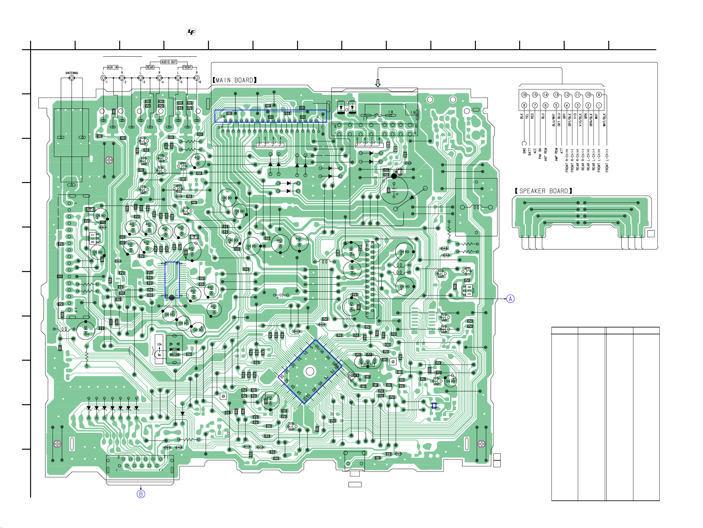
CDX-V3800
1-1. PRINTED WIRING BOARDS — MAIN SECTION — : Uses unleaded solder.
A
B
C
D
E
F
G
H
I
J
CDX-V3800
1
PJ601
TUX601
R615
R606
C612
R608
R607
JW47
JW48
C604
4
JW
3
JW
234567891011 12 13 14
PJ401
L602
JW60
JW59
JW58
R604
R603
JW150
61
JW
C602
R815
D817
C443
C619
JR10
C618
D600
C614
D815
Q601
50
JW
6
JW
C620
C409
D816
C439
C451
R430
R425
R468
51
JW
C108
R415
D301
R428
D814
5
JW
C450
C408
Q407
R441
Q404
C444
Q403
JW134
C420 C423
R414
C453
R426
JW145
JW144
54
52
JW
JW
FREQUENCY
SELECT
D813
D812
CNP800
KEY BOARD
CN901
C426
JW53
S800
D811
C436
R443
R420
JW128
R440
R412
55
JW
Q406
JW131
JW130
R416
C425
C452
R436
R413
R408
R409
R411
JW44
(Page 8)
Q405
JW121
C421
R435
56
JW
43
JW
C435
R442
R419
C422
R404
42
JW
D823
C440
JW127
Q401
D400
R406
C412
JR6
C424
JW57
S800
JW41
R421
C438
R405
IC401
D825
Q402
Q400
R417
R407
C454
39
JW
D820
C433C434
R418
R431
R429
R424
C428
C416
R800
R833
C430
L400
R402
R403
C437
R432
C413
46
JW
C417
C411
34
JW
45
JW
C106
JW151
40
JW
JW122
JW120
R447
28
JW
C113
C410
37
JW
JW126
JW125
JW124
JW123
C101
C446
C414
87
JW
FMB4
R809
C447
JW66
R400
36
JW
R832
R834
C107
C441
JW63
R401
27
JW
JW62
38
JW
R806
119
JW
IC100
R448
JW67
35
JW
R821
R805
30
JW
D802
C111
R823
R818
JW31
29
JW
R812
118
JW
R829
R828
R819
R801
R804
113
JW
64
JW
R849
D801
C991
117
JW
R813
R822
C993
R927
R830
R850
D904
116
JW
141
JW
R839
C821
R817
115
JW
JW65
R816
112
JW
C810
R840
C813
JW111
R427
D905
114
JW
26
JW
C809
R841
C807
R826
Q800
138
JW
D907
D922
D921
D702
C109
140
JW
68
JW
C994
YEL
D902
C990
110
JW
JW108
JW107
JW106
D908
D906
D909
105
104
JW
JW
L703
L700
JW72
JW76
JW74
JW73
JW143
R843
70
69
JW
JW
D701
IC801
C706
25
24
JW
JW
JW75
R705
X801
22
JW
R916
20
JW
D903
F900
CNP901
JW98JW109
142
JW
R931
101
JW
L701
L702
CN751
R709
C822
C992
49
JW
JW82
R703
C825
R810
JR12
R837
R860
FB901
YEL
JW92
FB902
D918
C922
C704
C705
FMB3
JR5
R901
JW85
R835
R848
R913
JW12
R845
D914
D919
11
JW
JW94
JW93
R903
R925
JW78
JW77
JW83
JW88
IC802
JW79
Q907
R902
Q900
D912
Q902
R904
R917
D915
JW84
JW97
JW96
JW95
C908
R701
Q906
Q701
JW80
JW8
JW9
R928
R912
Q703
L900
R702
R824
R825
JW81
JW86
1
SERVO
BOARD
CN1
200
JW
203
JW
204
JW
207
JW
2
4
3
• Semiconductor Location
Ref. No. Location
D301 E-2
D400 D-4
D600 E-2
D701 G-7
D702 G-6
D801 I-6
D802 I-5
D808 J-9
D811 I-3
D812 I-3
D813 I-3
D814 I-2
D815 I-2
D816 I-2
D916
D917
JW99
R932
JW100
103
102
JW
JW
91
JW
FB702
C711
C701
R708
C707
C709
R836
JW10
R846
R847
R936
R853
X800
R854
C817
C812
C816
R873
R814
D817 I-2
139
19
18
JW
JW
JW
JW17
S802
16
JW
C815
15
JW
R437
14
JW
D808
13
JW
2
JW
1-866-922-
1
JW
11
(11)
D820 I-4
D823 J-4
D825 J-4
D902 B-7
D903 B-8
D904 C-6
D905 C-6
D906 C-7
D907 C-6
D908 C-7
S802
RESET
D909 C-7
D912 E-10
D914 C-9
D915 E-10
201
JW
202
JW
205
JW
206
JW
5
Ref. No. Location
D916 C-8
D917 C-8
D918 C-9
D919 D-9
D921 D-6
D922 D-6
IC100 B-5
IC401 F-4
IC801 H-7
IC802 I-10
Q400 D-4
Q401 D-4
Q402 C-4
Q403 D-3
Q404 C-3
Q405 C-3
Q406 C-3
Q407 C-3
Q601 E-2
Q701 F-10
Q703 E-10
Q800 I-6
Q900 H-10
Q902 F-10
Q906 G-10
Q907 G-10
1-866-923-
8
7
6
11
44
Page 49

1-2. SCHEMATIC DIAGRAM — MAIN SECTION (1/3) — • Refer to page 10 for IC Block Diagrams.
CDX-V3800
C433
C434
C435
C436
PJ601
TUX601
R606
R604
R603
R608
R607
JR10
C612
C602
JW47
C614
C618
C619
Q601
D600
R615
C620
L602
R401
R400
C414
C413
C454
C412
C409
C408
C411
C410
R403
R402
IC401
IC B/D
R412
R411
R409
R407
R406
R405
R404
R408
R413
R435
R436
L400
C416
C417
C424
R416
C421
R421
C420
R420
C426
R415
C425
R414
R419
C423
C422
R418
C428
C450
C451 R443
C452
C453
R417
JR6
R440
R442
R441
Q406
Q407
Q405
Q404
Q403
Q402
R425 R426
R468
R428 R430
C108
D301
C440 R431
C444
C438
C437 R427
C439
C443
R432
R429
(Page 7)
D702
Q400
Q401
C430
D400
R424
(Page 6)
CDX-V3800
55
Page 50

CDX-V3800
1-3. SCHEMATIC DIAGRAM — MAIN SECTION (2/3) —
C113
C101
(Page 5)
C107
C993 C991
C990
C994
IC100
C106
C111
C109
D921
D922
D904
D903
D902
D905
D906
D907
D908
D909
D917
D916
FB901
FB902
R931
R932
R913
D914
D918
C922
CNP901
F900
L900
C992
D919
CDX-V3800
C446 R447
C441
R448
C447
(Page 7)
Q900
R903
C908
R902 R904
Q906
R824
Q907
Q902
D915
D912
R928
R917
R912
R825
C706
66
Page 51

1-4. SCHEMATIC DIAGRAM — MAIN SECTION (3/3) — • Refer to page 3 for Waveforms.
CDX-V3800
(Page 9)
CN751
CNP800
R843
C709
R708
R709
R703
C707
C701
FB702
D701
C704
C705
L700
L701
L702
C711
L703
R813
D820
R702
Q701
R701
Q703
C807 R826
S800
R805
R806
R833
R815
R800
R809
R814
(Page 5)
C809
C810
R901
C604
R834 R832
C813
C821
R801
R804
R850
D801
R849
Q800
R819
R818
R828
R830
R821
R823
R822
R835
R927
R916
R839
R840
R841
IC801
R816
R848
R873
R854
C816 C817
C812
X801
R705
JR12
R837
TP11
R845
R860
R836
R936
R853
C822
R925
R846
R847
R810
C825
JR5
X800
IC802
(Page 6)
CDX-V3800
D825
D817
D815
D816
D814
D813
D812
D811
D823
D802
R812
R817
77
C815
D808
R437
S802
Page 52

CDX-V3800
1-5. PRINTED WIRING BOARD — KEY SECTION — : Uses unleaded solder.
A
B
C
D
1
LED507,
S509
ATT
LED521,
S507
(VOLUME)
LED520,
S508
S509
LED507
LED521
LED520
S522
(OPEN)
234567891011 12 13 14
S513
LED501
(LCD BACK LIGHT)
LED501
LED525
S505 S506 S511
LED525,S505
MODE
LED522
LED522,S506
SEL
LED505
LED505,S511
1/REP
LED504
S512
LED504,S512
2/SHUF
LED503
(CD WINDOW)
LED503
LED511
S521 S520
LED511,S521
3/SLOW
LED510,S520
LED510
LCD501
S519
LED509,S519
LED509
5/OSD
LIQUID CRYSTAL DISPLAY PANEL
4/AUDIO
S518
LED508,S518
6/PAUSE
LED508
S510
LED506,S510
SENS/–
LED506
ALBUM
(LCD BACK LIGHT)
52
S523
LED518,S523
LED502
BTM/+
LED502
LED518
LED514,S515
EQ3
S515
LED514
LED512
S517
LED512,S517
SCRL
LED517
LED516
S514
S501
S501
EJECT
S522
S507
S508
S502
EJECT
S504
LED524,S504S502
SOURCE
LED513,S516
DSPL
S516
LED513
LED524
LED515
S503
3
2
1-866-924-
LED515,
S503
OFF
LED517,
S513
SEEK
LED516,
4
S514
IC502
1
11
(11)
E
F
G
H
R580
R507
R506
R505
R508
R578
R513
R533
R532
R504
R531
R579
• Semiconductor Location
Ref. No. Location
D502 F-13
D503 F-11
D504 F-13
D505 F-12
D551 G-10
D552 G-10
IC501 G-7
IC502 D-14
LED501 C-4
LED502 C-11
Ref. No. Location
LED503 B-8
LED504 D-6
LED505 D-6
LED506 D-10
LED507 A-1
LED508 D-10
LED509 D-9
LED510 D-8
LED511 D-7
LED512 D-12
LED513 C-3
LED514 C-12
R510
R509
R577
R576
R538
Ref. No. Location
LED515 A-14
LED516 C-14
LED517 B-14
LED518 D-11
LED520 C-2
LED521 B-2
LED522 D-5
LED524 D-3
LED525 D-4
Q502 G-10
R537
FM
R536
B3
R518
IC501
R517
R519
R555
R575
R516
R554
FM
R503
B4
R557
R574
R553
R514
C553
R515
C960
D551
R561
D552
R535
Q502
212
CN901
111
D505
R573
R560
D503
R552
R558
B
MAIN BOARD CNP800
(Page 4)
D504
R502
R559
R512
D502
R511
R501
R572
R551
R571
1-866-924-
C551
11
(11)
CDX-V3800
88
Page 53

1-6. SCHEMATIC DIAGRAM — KEY SECTION —
CN901
(Page 7)
D504
D503
D502
D505
R533
R532
R531
S522
LED503
R535
R538
R537
R536
LED501
LED502
R571 R573 R575 R577 R579
LED515
LED517
LED514
LED516
Q502
R572 R574 R576 R578 R580
LED512 LED509
LED518
LED506
LED508
LED510
LED511
LED504
LED505
LED522
LED525
LED524
LED513
LED521
LED507
LED520
R552
R551
IC502
C551
D551
R553
R554
R555
R558
R559
R560
CDX-V3800
C960
IC501
C553 R557
R561
D552
R511 R512 R513 R514 R515
S513
R501 R502 R504 R505 R506 R507 R508 R509 R510
S501
S502 S511S510
S505
S508 S509S504
R516
S519 S520 S523S515 S521S516
R503
S517S514
S506 S507S503
S518
R517
R518 R519
LCD501
S512
CDX-V3800
99
Page 54

CDX-V3800
• IC BLOCK DIAGRAMS
IC401 BD3806FS-E2 (MAIN Board (1/3))
DGND
32 31 30 29 28 27 26 25 24 23 22
SDA
SCL
MUTE
SEL
ADJ
VCC
VCC
OUTF1
OUTR1
OUTF2
OUTR2
NC
NC
21 20 19 18 17
NC
OUTS1
OUTS2
2
I
C BUS
LOGIC
BASS
fo:60,70,80,100,120,140,160,200Hz
Q:0.5,0.75,1,1.25
MIDDLE
fo:500Hz,1kHz
Q:1
TABLE
fo:5,7.5,10,12.5kHz
VCO
FADER
(0~-58,
-∞dB)
EFFECT (0dB~
+20dB,2dB STEP)
TONE
PASS
fc:40kHz fc:40kHz
(0~15dB,1dB STEP)
(4 STEREO INCLUDE 1 ISOLATION INPUT)
FADER
(0~-58,
-∞dB)
BASS,TREBLE, MIDDLE
(-15dB~+15dB,1dB STEP)
VOLUME
(+23~-79dB,-∞dB
1dB STEP)
ANTI-ALIASING
FILTER
INPUT GAIN
MUTE
INPUT SELECTOR
TONE
PASS
FADER
(0~-58,
-∞dB)
EFFECT (0dB~
+20dB,2dB STEP)
BASS,TREBLE, MIDDLE
(-15dB~+15dB,1dB STEP)
VOLUME
(+23~-79dB,-∞dB
1dB STEP)
ANTI-ALIASING
FILTER
INPUT GAIN
(0~15dB,1dB STEP)
MUTE
FADER
(0~-58,
-∞dB)
2ND ORDER LPF
fc:OFF,80,120,160Hz
Q: 0.707
MIX
GAIN+ATT
(+10~-29,
-∞dB)
2ND ORDER
LPF
AGND
VCC/2
6 7 8 9 10 113 4 521
AP1
AN
FIL
AP2
B1
B2
C2
C1
NC
NC
12 14 1613 15
NC
NC
NC
NC
NC
CDX-V3800
1010
Page 55

NOTE:
2
• The mechanical parts with no reference
number in the exploded views are not supplied.
• Items marked “*” are not stocked since
they are seldom required for routine service.
Some delay should be anticipated
when ordering these items.
• -XX and -X mean standardized parts, so
they may have some difference from the
original one.
2-1. MAIN SECTION
SECTION 2
EXPLODED VIEWS
• Color Indication of Appearance Parts
Example :
KNOB, BALANCE (WHITE) ... (RED)
RR
Parts Color Cabinet’s Color
• Accessories are given in the last of this
parts list.
CDX-V3800
The components identified by
mark 0 or dotted line with mark
0 are critical for safety.
Replace only with part number
specified.
MG-611MM-186//Q
not supplied
#1
B
A
not supplied
10
3
A
9
#3
6
5
#2
8
F901
#
4
#1
not supplied
7
TUX601
2
#1
Ref. No. Part No. Description Remark
1 X-3384-176-3 PANEL ASSY, SUB
23-042-244-11 SCREW (T)
3 X-3383-739-1 LOCK ASSY (S)
42-021-848-01 SHEET (TU), GROUND
52-050-124-01 SCREW +BTT 2.6X5
61-829-847-11 CABLE, FLAT (FFC) 26P
7 A-1115-219-A MAIN BOARD, COMPLETE
81-792-194-61 CORD (WITH CONNECTOR) (POWER)
B
#1
not supplied
1
Ref. No. Part No. Description Remark
9 1-829-836-12 CORD, CONNECTION (VIDEO) (VIDEO OUT)
10 2-596-791-01 SHEET, SHIELD
F901 1-532-877-11 FUSE (BLADE TYPE) (AUTO FUSE) 10A
TUX601 A-3220-961-A TUNER UNIT (TUX-032)
#1 7-685-792-09 SCREW +PTT 2.6X6 (S)
#2 7-685-793-09 SCREW +PTT 2.6X8 (S)
#3 7-685-790-01 SCREW +PTT 2.6X4 (S)
11
Page 56
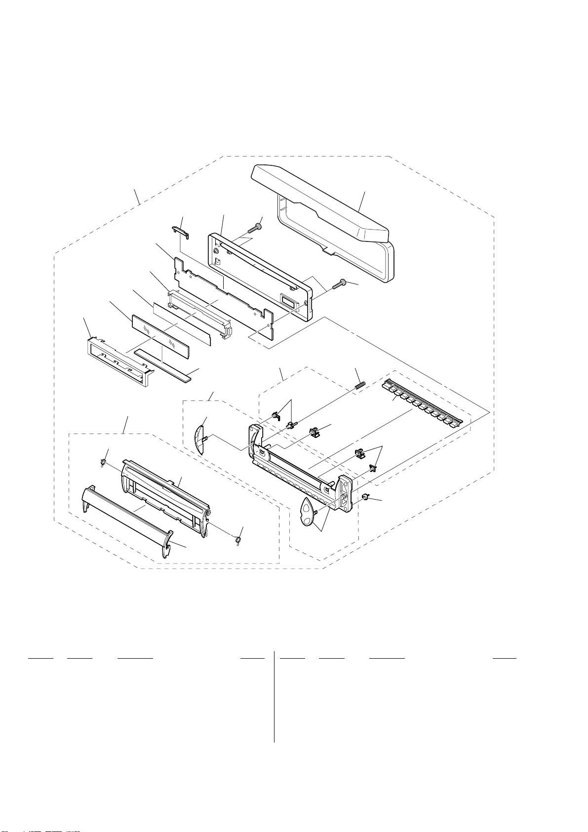
CDX-V3800
2-2. FRONT PANEL SECTION
LCD501
not supplied
not supplied
61
not supplied
(KEY board)
not supplied
57
51
58
53
not supplied
63
59
62
55
not supplied
56
not
supplied
60
62
not
supplied
not supplied
not supplied
54
51 A-1122-750-A RETRACTABLE ASSY
52 3-258-947-02 FILTER (IR)
53 1-780-096-11 CONDUCTIVE BOARD, CONNECTION
54 X-2059-418-1 SHUTTER (SV) ASSY
55 X-2059-416-1 BUTTON ASSY (SV)
56 3-246-479-01 SPRING (RELEASE)
57 2-515-402-01 SHEET (ILLUMINATOR)
52
not supplied
not supplied
Ref. No. Part No. Description RemarkRef. No. Part No. Description Remark
58 2-188-139-01 PLATE (CD), LIGHT GUIDE
59 3-258-937-01 PANEL, FRONT BACK
60 X-3385-071-1 CASE ASSY (for FRONT PANEL)
61 A-1115-222-A PANEL OVERALL ASSY, FRONT
62 3-250-543-21 SCREW (+B P-TITE M2)
63 X-2059-417-1 PANEL ASSY, FRONT (SV)
LCD501 1-805-451-11 DISPLAY PANEL, LIQUID CRYSTAL
12
Page 57

2-3. CD MECHANISM SECTION (1)
(MG-611MM-186//Q)
CDX-V3800
109
not supplied
102
not supplied
(SENSOR board)
110
not supplied
101
#4
103
104
106
105
108
107
Ref. No. Part No. Description Remark Ref. No. Part No. Description Remark
101 A-3372-444-A CHASSIS (T) SUB ASSY
102 3-253-729-11 SPRING (LTR), TENSION COIL
103 3-257-892-12 SPRING (DAMPER), COIL
104 3-257-892-01 SPRING (DAMPER), COIL
105 2-345-767-11 SPRING (KF60), TENSION
106 3-259-033-01 DAMPER (S)
107 2-587-505-01 SCREW
108 A-1107-620-A SERVO BOARD, COMPLETE
109 X-3384-088-2 LEVER (L) ASSY
110 X-3384-089-2 LEVER (R) ASSY
#4 7-627-552-87 SCREW, PRECISION +P 1.7X2.2
13
Page 58

CDX-V3800
2-4. CD MECHANISM SECTION (2)
(MG-611MM-186//Q)
154
(including M901)
155
156
157
#5
SW4
151
not supplied
M902
not supplied
not supplied
not supplied
153
not supplied
152
Ref. No. Part No. Description Remark Ref. No. Part No. Description Remark
151 A-1075-644-A CHASSIS (OP) COMPLETE ASSY
152 3-316-938-91 SCREW (B1.4X5), TAPPING
0 153 8-820-207-12 OPTICAL PICK-UP (KSS1000E/K1RP)
154 A-1075-645-A CHASSIS (OP) SUB ASSY (including M901)
155 A-3372-449-A ARM SUB ASSY, CHUCKING
156 A-3372-446-A LEVER (SL) SUB ASSY
157 X-3384-090-2 LEVER (SL) ASSY
M902 A-3372-447-A MOTOR ASSY, SL (SLED)
SW4 1-571-099-11 SWITCH (1 KEY) (LIMIT)
#5 7-627-850-77 SCREW, PRECISION +P 1.4X1.8
14
Page 59

2-5. CD MECHANISM SECTION (3)
(MG-611MM-186//Q)
CDX-V3800
209
207
208
201
202
207
#4
M903
206
207
210
203
211
204
205
Ref. No. Part No. Description Remark Ref. No. Part No. Description Remark
201 3-348-993-01 WASHER
202 2-186-699-01 GEAR (RA1)
203 A-1075-641-B ARM ASSY, ROLLER
204 3-259-455-12 SPRING (RAL)
205 3-253-713-11 SPRING (RAR)
206 3-259-469-12 SPRING (LE), LEAF
207 2-134-636-21 SCREW (M1.7X2.5)
208 2-186-696-01 BRACKET (LEM-N)
209 3-345-648-91 SCREW (M1.4), TOOTHED LOCK
210 A-1083-636-A GEAR (LE) ASSY
211 2-186-697-01 BEARING (LEB-N)
M903 A-1075-643-A MOTOR ASSY, LE (LOADING)
#4 7-627-552-87 SCREW, PRECISION +P 1.7X2.2
15
Page 60
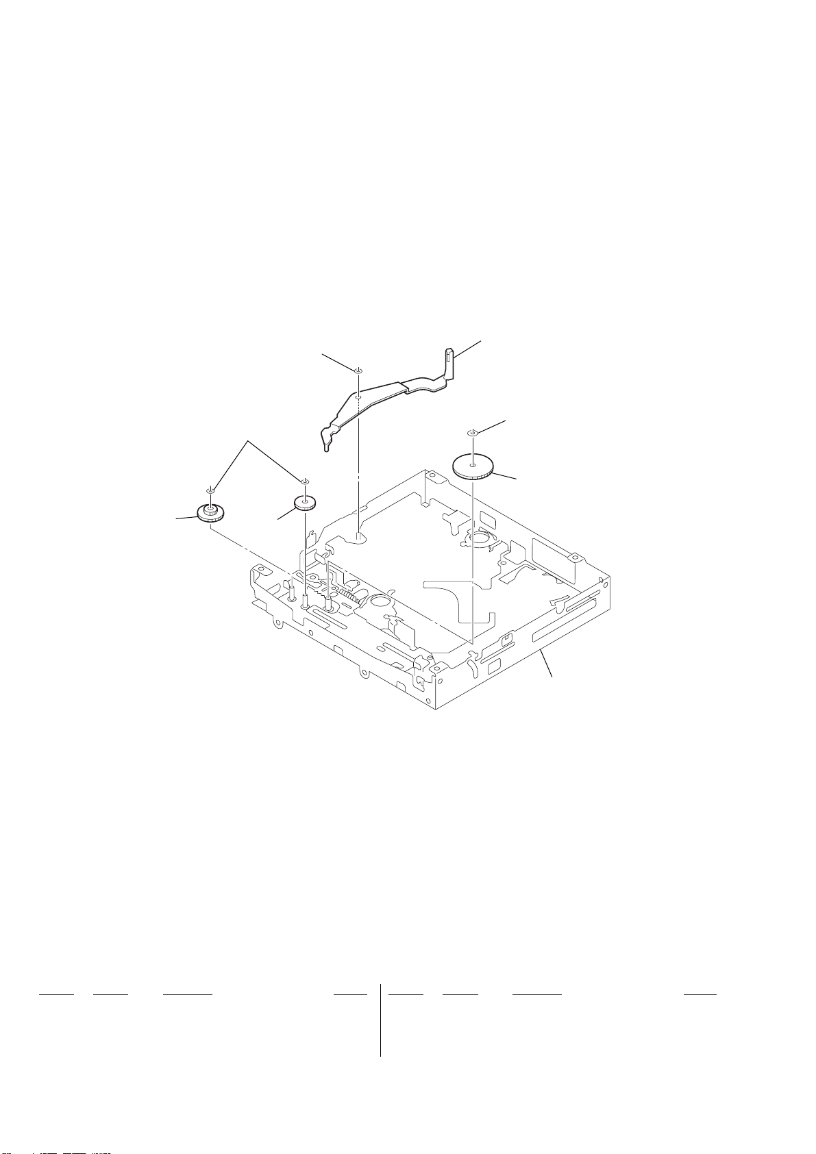
CDX-V3800
2-6. CD MECHANISM SECTION (4)
(MG-611MM-186//Q)
252
254
252
255
251
256
253
257
Ref. No. Part No. Description Remark Ref. No. Part No. Description Remark
251 2-186-700-01 GEAR (CHK1)
252 3-344-223-01 WASHER
253 3-259-470-11 GEAR (LE1)
254 3-253-755-12 LEVER (D)
255 2-630-962-01 WASHER (SLIT)
* 256 2-590-545-01 GEAR (LE2-M)
257 A-1075-640-B CHASSIS (M) BLOCK ASSY
16
Page 61

CDX-V3800
SECTION 3
ELECTRICAL PARTS LIST
NOTE:
• Due to standardization, replacements in
the parts list may be different from the
parts specified in the diagrams or the
components used on the set.
• -XX and -X mean standardized parts, so
they may have some difference from the
original one.
• RESISTORS
All resistors are in ohms.
METAL:Metal-film resistor.
METAL OXIDE: Metal oxide-film resistor.
F:nonflammable
Ref. No. Part No. Description Remark Ref. No. Part No. Description Remark
KEY BOARD
**********
1-780-096-11 CONDUCTIVE BOARD, CONNECTION
2-515-402-01 SHEET (ILLUMINATOR)
• Items marked “*” are not stocked since
they are seldom required for routine service.
Some delay should be anticipated
when ordering these items.
• SEMICONDUCTORS
In each case, u : µ, for example:
uA.. : µA.. uPA.. : µPA..
uPB.. : µPB.. uPC.. : µPC.. uPD.. : µPD..
• CAPACITORS
uF : µF
• COILS
uH : µH
LED515 8-719-053-09 LED SML-310VTT86 (OFF)
LED516 8-719-053-09 LED SML-310VTT86 (SEEK –/m .)
LED517 8-719-053-09 LED SML-310VTT86 (SEEK +/> M)
LED518 8-719-053-09 LED SML-310VTT86 (BTM/ALBUM +)
LED520 8-719-053-09 LED SML-310VTT86 (VOL –)
The components identified by
mark 0 or dotted line with mark
0 are critical for safety.
Replace only with part number
specified.
When indicating parts by reference
number, please include the board.
KEY
< CAPACITOR >
C551 1-164-227-11 CERAMIC CHIP 0.022uF 10% 25V
C553 1-125-891-11 CERAMIC CHIP 0.47uF 10% 10V
C960 1-107-826-11 CERAMIC CHIP 0.1uF 10% 16V
< CONNECTOR >
CN901 1-794-312-11 PIN, CONNECTOR 12P
< DIODE >
D502 8-719-056-83 DIODE UDZ-TE-17-6.8B
D503 8-719-056-83 DIODE UDZ-TE-17-6.8B
D504 8-719-056-83 DIODE UDZ-TE-17-6.8B
D505 8-719-056-83 DIODE UDZ-TE-17-6.8B
D551 8-719-976-99 DIODE DTZ5.1B
D552 8-719-988-61 DIODE 1SS355TE-17
< IC >
IC501 6-707-063-01 IC LC75826WH-US-E
IC502 6-600-163-01 IC RS-770 (IR)
< LIQUID CRYSTAL DISPLAY >
LCD501 1-805-451-11 DISPLAY PANEL, LIQUID CRYSTAL
LED521 8-719-053-09 LED SML-310VTT86 (VOL +)
LED522 8-719-053-09 LED SML-310VTT86 (SEL)
LED524 8-719-053-09 LED SML-310VTT86 (SOURCE)
LED525 8-719-053-09 LED SML-310VTT86 (MODE)
< TRANSISTOR >
Q502 6-551-244-01 TRANSISTOR MUN2233T1G
< RESISTOR >
R501 1-216-819-11 METAL CHIP 680 5% 1/10W
R502 1-216-819-11 METAL CHIP 680 5% 1/10W
R503 1-216-823-11 METAL CHIP 1.5K 5% 1/10W
R504 1-216-819-11 METAL CHIP 680 5% 1/10W
R505 1-216-821-11 METAL CHIP 1K 5% 1/10W
R506 1-216-823-11 METAL CHIP 1.5K 5% 1/10W
R507 1-216-823-11 METAL CHIP 1.5K 5% 1/10W
R508 1-216-825-11 METAL CHIP 2.2K 5% 1/10W
R509 1-216-827-11 METAL CHIP 3.3K 5% 1/10W
R510 1-216-829-11 METAL CHIP 4.7K 5% 1/10W
R511 1-216-819-11 METAL CHIP 680 5% 1/10W
R512 1-216-819-11 METAL CHIP 680 5% 1/10W
R513 1-216-819-11 METAL CHIP 680 5% 1/10W
R514 1-216-821-11 METAL CHIP 1K 5% 1/10W
R515 1-216-823-11 METAL CHIP 1.5K 5% 1/10W
< DIODE >
LED501 6-501-062-01 LED NSCW505CT-AST (LCD BACK LIGHT)
LED502 6-501-062-01 LED NSCW505CT-AST (LCD BACK LIGHT)
LED503 8-719-053-09 LED SML-310VTT86 (CD WINDOW)
LED504 8-719-053-09 LED SML-310VTT86 (2/SHUF)
LED505 8-719-053-09 LED SML-310VTT86 (1/REP)
LED506 8-719-053-09 LED SML-310VTT86 (SENS/ALBUM –)
LED507 8-719-053-09 LED SML-310VTT86 (ATT)
LED508 8-719-053-09 LED SML-310VTT86 (6/PAUSE)
LED509 8-719-053-09 LED SML-310VTT86 (5/OSD)
LED510 8-719-053-09 LED SML-310VTT86 (4/AUDIO)
LED511 8-719-053-09 LED SML-310VTT86 (3/SLOW)
LED512 8-719-053-09 LED SML-310VTT86 (SCRL)
LED513 8-719-053-09 LED SML-310VTT86 (DSPL)
LED514 8-719-053-09 LED SML-310VTT86 (EQ3)
R516 1-216-825-11 METAL CHIP 2.2K 5% 1/10W
R517 1-216-827-11 METAL CHIP 3.3K 5% 1/10W
R518 1-216-829-11 METAL CHIP 4.7K 5% 1/10W
R519 1-218-867-11 METAL CHIP 6.8K 0.5% 1/10W
R531 1-216-813-11 METAL CHIP 220 5% 1/10W
R532 1-216-813-11 METAL CHIP 220 5% 1/10W
R533 1-216-813-11 METAL CHIP 220 5% 1/10W
R535 1-216-815-11 METAL CHIP 330 5% 1/10W
R536 1-216-807-11 METAL CHIP 68 5% 1/10W
R537 1-216-807-11 METAL CHIP 68 5% 1/10W
R538 1-216-807-11 METAL CHIP 68 5% 1/10W
R551 1-216-815-11 METAL CHIP 330 5% 1/10W
R552 1-216-815-11 METAL CHIP 330 5% 1/10W
R553 1-216-821-11 METAL CHIP 1K 5% 1/10W
R554 1-216-821-11 METAL CHIP 1K 5% 1/10W
17
Page 62

CDX-V3800
MAINKEY
Ref. No. Part No. Description Remark Ref. No. Part No. Description Remark
R555 1-216-821-11 METAL CHIP 1K 5% 1/10W
R557 1-216-821-11 METAL CHIP 1K 5% 1/10W
R558 1-216-821-11 METAL CHIP 1K 5% 1/10W
R559 1-216-821-11 METAL CHIP 1K 5% 1/10W
R560 1-216-821-11 METAL CHIP 1K 5% 1/10W
C408 1-115-467-11 CERAMIC CHIP 0.22uF 10% 10V
C409 1-115-467-11 CERAMIC CHIP 0.22uF 10% 10V
C410 1-126-960-11 ELECT 1uF 20% 50V
C411 1-126-960-11 ELECT 1uF 20% 50V
C412 1-126-960-11 ELECT 1uF 20% 50V
R561 1-216-857-11 METAL CHIP 1M 5% 1/10W
R571 1-216-809-11 METAL CHIP 100 5% 1/10W
R572 1-216-809-11 METAL CHIP 100 5% 1/10W
R573 1-216-809-11 METAL CHIP 100 5% 1/10W
R574 1-216-809-11 METAL CHIP 100 5% 1/10W
R575 1-216-809-11 METAL CHIP 100 5% 1/10W
R576 1-216-809-11 METAL CHIP 100 5% 1/10W
R577 1-216-809-11 METAL CHIP 100 5% 1/10W
R578 1-216-809-11 METAL CHIP 100 5% 1/10W
R579 1-216-809-11 METAL CHIP 100 5% 1/10W
R580 1-216-809-11 METAL CHIP 100 5% 1/10W
< SWITCH >
S501 1-786-653-11 SWITCH, TACTILE (EJECT)
S502 1-786-653-11 SWITCH, TACTILE (EJECT)
S503 1-786-653-11 SWITCH, TACTILE (OFF)
S504 1-786-653-11 SWITCH, TACTILE (SOURCE)
S505 1-786-653-11 SWITCH, TACTILE (MODE)
S506 1-786-653-11 SWITCH, TACTILE (SEL)
S507 1-786-653-11 SWITCH, TACTILE (VOL +)
S508 1-786-653-11 SWITCH, TACTILE (VOL –)
S509 1-786-653-11 SWITCH, TACTILE (ATT)
S510 1-786-653-11 SWITCH, TACTILE (SENS/ALBUM –)
S511 1-786-653-11 SWITCH, TACTILE (1/REP)
S512 1-786-653-11 SWITCH, TACTILE (2/SHUF)
S513 1-786-653-11 SWITCH, TACTILE (SEEK +/> M)
S514 1-786-653-11 SWITCH, TACTILE (SEEK –/m .)
S515 1-786-653-11 SWITCH, TACTILE (EQ3)
S516 1-786-653-11 SWITCH, TACTILE (DSPL)
S517 1-786-653-11 SWITCH, TACTILE (SCRL)
S518 1-786-653-11 SWITCH, TACTILE (6/PAUSE)
S519 1-786-653-11 SWITCH, TACTILE (5/OSD)
S520 1-786-653-11 SWITCH, TACTILE (4/AUDIO)
S521 1-786-653-11 SWITCH, TACTILE (3/SLOW)
S522 1-529-566-61 SWITCH, PUSH (1 KEY) (OPEN)
S523 1-786-653-11 SWITCH, TACTILE (BTM/ALBUM +)
*************************************************************
A-1115-219-A MAIN BOARD, COMPLETE
(including SPEAKER BOARD)
*********************
7-685-134-19 SCREW +P 2.6X8 TYPE2 NON-SLIT
7-685-794-09 SCREW +PTT 2.6X10 (S)
7-685-795-09 SCREW +PTT 2.6X12 (S)
< CAPACITOR >
C101 1-126-964-11 ELECT 10uF 20% 50V
C106 1-126-965-11 ELECT 22uF 20% 50V
C107 1-126-964-11 ELECT 10uF 20% 50V
C108 1-162-964-11 CERAMIC CHIP 0.001uF 10% 50V
C109 1-104-665-11 ELECT 100uF 20% 25V
C111 1-126-964-11 ELECT 10uF 20% 50V
C113 1-107-823-11 CERAMIC CHIP 0.47uF 10% 16V
C413 1-126-960-11 ELECT 1uF 20% 50V
C414 1-126-964-11 ELECT 10uF 20% 50V
C416 1-162-970-11 CERAMIC CHIP 0.01uF 10% 25V
C417 1-126-947-11 ELECT 47uF 20% 35V
C420 1-162-927-11 CERAMIC CHIP 100PF 5% 50V
C421 1-162-927-11 CERAMIC CHIP 100PF 5% 50V
C422 1-162-927-11 CERAMIC CHIP 100PF 5% 50V
C423 1-162-927-11 CERAMIC CHIP 100PF 5% 50V
C424 1-126-964-11 ELECT 10uF 20% 50V
C425 1-126-964-11 ELECT 10uF 20% 50V
C426 1-126-964-11 ELECT 10uF 20% 50V
C428 1-126-964-11 ELECT 10uF 20% 50V
C430 1-126-947-11 ELECT 47uF 20% 35V
C433 1-162-927-11 CERAMIC CHIP 100PF 5% 50V
C434 1-162-927-11 CERAMIC CHIP 100PF 5% 50V
C435 1-162-927-11 CERAMIC CHIP 100PF 5% 50V
C436 1-162-927-11 CERAMIC CHIP 100PF 5% 50V
C437 1-107-823-11 CERAMIC CHIP 0.47uF 10% 16V
C438 1-107-823-11 CERAMIC CHIP 0.47uF 10% 16V
C439 1-162-927-11 CERAMIC CHIP 100PF 5% 50V
C440 1-107-823-11 CERAMIC CHIP 0.47uF 10% 16V
C441 1-115-467-11 CERAMIC CHIP 0.22uF 10% 10V
C443 1-162-927-11 CERAMIC CHIP 100PF 5% 50V
C444 1-107-823-11 CERAMIC CHIP 0.47uF 10% 16V
C446 1-162-923-11 CERAMIC CHIP 47PF 5% 50V
C447 1-126-961-11 ELECT 2.2uF 20% 50V
C450 1-162-927-11 CERAMIC CHIP 100PF 5% 50V
C451 1-162-927-11 CERAMIC CHIP 100PF 5% 50V
C452 1-126-964-11 ELECT 10uF 20% 50V
C453 1-126-964-11 ELECT 10uF 20% 50V
C454 1-126-964-11 ELECT 10uF 20% 50V
C602 1-126-964-11 ELECT 10uF 20% 50V
C604 1-162-927-11 CERAMIC CHIP 100PF 5% 50V
C612 1-162-964-11 CERAMIC CHIP 0.001uF 10% 50V
C614 1-115-156-11 CERAMIC CHIP 1uF 10V
C618 1-126-947-11 ELECT 47uF 20% 35V
C619 1-126-964-11 ELECT 10uF 20% 50V
C620 1-107-826-11 CERAMIC CHIP 0.1uF 10% 16V
C701 1-124-584-00 ELECT 100uF 20% 10V
C704 1-124-584-00 ELECT 100uF 20% 10V
C705 1-124-584-00 ELECT 100uF 20% 10V
C706 1-162-964-11 CERAMIC CHIP 0.001uF 10% 50V
C707 1-124-584-00 ELECT 100uF 20% 10V
C709 1-162-964-11 CERAMIC CHIP 0.001uF 10% 50V
C711 1-124-589-11 ELECT 47uF 20% 16V
C807 1-162-970-11 CERAMIC CHIP 0.01uF 10% 25V
C809 1-104-665-11 ELECT 100uF 20% 25V
C810 1-125-701-22 DOUBLE LAYERS 0.47F 5.5V
C812 1-107-826-11 CERAMIC CHIP 0.1uF 10% 16V
C813 1-104-665-11 ELECT 100uF 20% 25V
C815 1-162-964-11 CERAMIC CHIP 0.001uF 10% 50V
C816 1-162-917-11 CERAMIC CHIP 15PF 5% 50V
C817 1-162-917-11 CERAMIC CHIP 15PF 5% 50V
18
Page 63

CDX-V3800
MAIN
Ref. No. Part No. Description Remark Ref. No. Part No. Description Remark
C821 1-107-826-11 CERAMIC CHIP 0.1uF 10% 16V
C822 1-107-826-11 CERAMIC CHIP 0.1uF 10% 16V
C825 1-104-665-11 ELECT 100uF 20% 25V
C908 1-123-611-61 ELECT 1uF 20% 50V
C922 1-131-868-81 ELECT 3300uF 20% 16V
C990 1-115-340-11 CERAMIC CHIP 0.22uF 10% 25V
C991 1-115-340-11 CERAMIC CHIP 0.22uF 10% 25V
C992 1-115-340-11 CERAMIC CHIP 0.22uF 10% 25V
C993 1-115-340-11 CERAMIC CHIP 0.22uF 10% 25V
C994 1-115-340-11 CERAMIC CHIP 0.22uF 10% 25V
< CONNECTOR >
IC100 6-705-360-02 IC TDA8588BJ/N2/R1
IC401 6-705-372-01 IC BD3808FS-FE2
IC801 6-805-155-01 IC MB90488BPF-G-135-BNDE1
IC802 8-759-659-13 IC PST3428UL
JR5 1-216-864-11 SHORT CHIP 0
JR6 1-216-864-11 SHORT CHIP 0
JR10 1-414-227-11 INDUCTOR, FERRITE BEAD
JR12 1-216-864-11 SHORT CHIP 0
< IC >
< JUMPER RESISTOR >
CN751 1-779-294-11 CONNECTOR, FFC (LIF(NON-ZIF)) 26P
CNP800 1-794-311-21 PLUG, CONNECTOR 12P
CNP901 1-774-701-21 PIN, CONNECTOR 16P
< DIODE >
D301 8-719-056-83 DIODE UDZ-TE-17-6.8B
D400 8-719-081-97 DIODE MMDL914T1
D600 8-719-036-94 DIODE RD5.6SB-T1
D701 8-719-081-97 DIODE MMDL914T1
D702 8-719-081-97 DIODE MMDL914T1
D801 8-719-081-97 DIODE MMDL914T1
D802 8-719-058-24 DIODE RB501V-40TE-17
D808 8-719-056-83 DIODE UDZ-TE-17-6.8B
D811 8-719-109-97 DIODE RD6.8ESB2
D812 8-719-109-97 DIODE RD6.8ESB2
D813 8-719-109-97 DIODE RD6.8ESB2
D814 8-719-109-97 DIODE RD6.8ESB2
D815 8-719-109-97 DIODE RD6.8ESB2
D816 8-719-109-97 DIODE RD6.8ESB2
D817 8-719-109-97 DIODE RD6.8ESB2
D820 8-719-991-33 DIODE 1SS133T-77
D823 8-719-056-93 DIODE UDZ-TE-17-18B
D825 8-719-056-93 DIODE UDZ-TE-17-18B
D902 8-719-053-18 DIODE 1SR154-400TE-25
D903 8-719-053-18 DIODE 1SR154-400TE-25
D904 6-500-522-01 DIODE 10EDB40-TA1B2
D905 6-500-522-01 DIODE 10EDB40-TA1B2
D906 6-500-522-01 DIODE 10EDB40-TA1B2
D907 6-500-522-01 DIODE 10EDB40-TA1B2
D908 6-500-522-01 DIODE 10EDB40-TA1B2
D909 6-500-522-01 DIODE 10EDB40-TA1B2
D912 8-719-056-93 DIODE UDZ-TE-17-18B
D914 8-719-056-83 DIODE UDZ-TE-17-6.8B
D915 8-719-056-83 DIODE UDZ-TE-17-6.8B
D916 6-500-522-01 DIODE 10EDB40-TA1B2
< COIL >
JW47 1-410-501-11 INDUCTOR 2.2uH
L400 1-414-398-11 INDUCTOR 10uH
L602 1-414-394-41 INDUCTOR 2.2uH
L700 1-410-509-11 INDUCTOR 10uH
L701 1-410-501-11 INDUCTOR 2.2uH
L702 1-410-509-11 INDUCTOR 10uH
L703 1-414-813-11 FERRITE, EMI (SMD) (2012)
L900 1-456-617-11 COIL, CHOKE 250uH
< JACK >
PJ401 1-774-700-11 JACK, PIN 6P (AUX IN,
AUDIO OUT FRONT/REAR)
PJ601 1-815-185-13 JACK (ANTENNA)
< TRANSISTOR >
Q400 8-729-421-19 TRANSISTOR UN2213
Q401 8-729-424-08 TRANSISTOR UN2111
Q402 6-551-070-01 TRANSISTOR KRC283S-B-RPK/P
Q403 6-551-070-01 TRANSISTOR KRC283S-B-RPK/P
Q404 6-551-070-01 TRANSISTOR KRC283S-B-RPK/P
Q405 6-551-070-01 TRANSISTOR KRC283S-B-RPK/P
Q406 6-551-070-01 TRANSISTOR KRC283S-B-RPK/P
Q407 6-551-070-01 TRANSISTOR KRC283S-B-RPK/P
Q601 8-729-920-85 TRANSISTOR 2SD1664-QR
Q701 8-729-106-60 TRANSISTOR 2SB1115A-YQ
Q703 8-729-027-46 TRANSISTOR DTC114YKA-T146
Q800 8-729-424-08 TRANSISTOR UN2111
Q900 8-729-010-25 TRANSISTOR MSD601-RT1
Q902 8-729-421-22 TRANSISTOR UN2211
Q906 8-729-010-25 TRANSISTOR MSD601-RT1
Q907 8-729-421-19 TRANSISTOR UN2213
< RESISTOR >
D917 6-500-522-01 DIODE 10EDB40-TA1B2
D918 8-719-987-69 DIODE DAN217
D919 8-719-049-38 DIODE 1N5404TU
D921 6-500-522-01 DIODE 10EDB40-TA1B2
D922 6-500-522-01 DIODE 10EDB40-TA1B2
< FERRITE BEAD >
FB702 1-414-813-11 FERRITE, EMI (SMD) (2012)
FB901 1-414-813-11 FERRITE, EMI (SMD) (2012)
FB902 1-414-813-11 FERRITE, EMI (SMD) (2012)
R402 1-216-864-11 SHORT CHIP 0
R403 1-216-864-11 SHORT CHIP 0
R404 1-216-809-11 METAL CHIP 100 5% 1/10W
R405 1-216-809-11 METAL CHIP 100 5% 1/10W
R406 1-216-809-11 METAL CHIP 100 5% 1/10W
R407 1-216-809-11 METAL CHIP 100 5% 1/10W
R408 1-216-864-11 SHORT CHIP 0
R409 1-218-881-11 METAL CHIP 27K 0.5% 1/10W
R411 1-216-809-11 METAL CHIP 100 5% 1/10W
R412 1-216-809-11 METAL CHIP 100 5% 1/10W
19
Page 64

CDX-V3800
MAIN
Ref. No. Part No. Description Remark Ref. No. Part No. Description Remark
R413 1-216-864-11 SHORT CHIP 0
R414 1-216-809-11 METAL CHIP 100 5% 1/10W
R415 1-216-809-11 METAL CHIP 100 5% 1/10W
R416 1-216-809-11 METAL CHIP 100 5% 1/10W
R417 1-216-809-11 METAL CHIP 100 5% 1/10W
R824 1-216-849-11 METAL CHIP 220K 5% 1/10W
R825 1-216-849-11 METAL CHIP 220K 5% 1/10W
R826 1-216-843-11 METAL CHIP 68K 5% 1/10W
R828 1-216-809-11 METAL CHIP 100 5% 1/10W
R830 1-216-809-11 METAL CHIP 100 5% 1/10W
R418 1-216-841-11 METAL CHIP 47K 5% 1/10W
R419 1-216-841-11 METAL CHIP 47K 5% 1/10W
R420 1-216-841-11 METAL CHIP 47K 5% 1/10W
R421 1-216-841-11 METAL CHIP 47K 5% 1/10W
R424 1-216-805-11 METAL CHIP 47 5% 1/10W
R425 1-216-833-11 METAL CHIP 10K 5% 1/10W
R426 1-216-824-11 METAL CHIP 1.8K 5% 1/10W
R427 1-216-809-11 METAL CHIP 100 5% 1/10W
R428 1-216-833-11 METAL CHIP 10K 5% 1/10W
R429 1-247-807-31 CARBON 100 5% 1/4W
R430 1-216-824-11 METAL CHIP 1.8K 5% 1/10W
R431 1-247-807-31 CARBON 100 5% 1/4W
R432 1-216-809-11 METAL CHIP 100 5% 1/10W
R435 1-216-809-11 METAL CHIP 100 5% 1/10W
R436 1-216-809-11 METAL CHIP 100 5% 1/10W
R437 1-216-821-11 METAL CHIP 1K 5% 1/10W
R440 1-216-809-11 METAL CHIP 100 5% 1/10W
R441 1-216-809-11 METAL CHIP 100 5% 1/10W
R442 1-216-841-11 METAL CHIP 47K 5% 1/10W
R443 1-216-841-11 METAL CHIP 47K 5% 1/10W
R447 1-216-811-11 METAL CHIP 150 5% 1/10W
R448 1-216-841-11 METAL CHIP 47K 5% 1/10W
R468 1-216-789-11 METAL CHIP 2.2 5% 1/10W
R603 1-247-807-31 CARBON 100 5% 1/4W
R604 1-247-807-31 CARBON 100 5% 1/4W
R832 1-216-825-11 METAL CHIP 2.2K 5% 1/10W
R833 1-249-417-11 CARBON 1K 5% 1/4W
R834 1-216-825-11 METAL CHIP 2.2K 5% 1/10W
R835 1-216-845-11 METAL CHIP 100K 5% 1/10W
R836 1-216-845-11 METAL CHIP 100K 5% 1/10W
R837 1-216-821-11 METAL CHIP 1K 5% 1/10W
R839 1-216-809-11 METAL CHIP 100 5% 1/10W
R840 1-216-809-11 METAL CHIP 100 5% 1/10W
R841 1-216-809-11 METAL CHIP 100 5% 1/10W
R843 1-216-809-11 METAL CHIP 100 5% 1/10W
R846 1-216-845-11 METAL CHIP 100K 5% 1/10W
R847 1-216-845-11 METAL CHIP 100K 5% 1/10W
R848 1-216-845-11 METAL CHIP 100K 5% 1/10W
R849 1-216-841-11 METAL CHIP 47K 5% 1/10W
R850 1-218-871-11 METAL CHIP 10K 0.5% 1/10W
R853 1-216-864-11 SHORT CHIP 0
R854 1-216-864-11 SHORT CHIP 0
R860 1-216-845-11 METAL CHIP 100K 5% 1/10W
R873 1-216-845-11 METAL CHIP 100K 5% 1/10W
R901 1-216-845-11 METAL CHIP 100K 5% 1/10W
R902 1-216-829-11 METAL CHIP 4.7K 5% 1/10W
R903 1-216-841-11 METAL CHIP 47K 5% 1/10W
R904 1-216-841-11 METAL CHIP 47K 5% 1/10W
R912 1-249-417-11 CARBON 1K 5% 1/4W
R913 1-216-821-11 METAL CHIP 1K 5% 1/10W
R606 1-216-809-11 METAL CHIP 100 5% 1/10W
R607 1-216-809-11 METAL CHIP 100 5% 1/10W
R608 1-216-809-11 METAL CHIP 100 5% 1/10W
R615 1-216-821-11 METAL CHIP 1K 5% 1/10W
R701 1-216-057-00 RES-CHIP 2.2K 5% 1/10W
R702 1-216-033-00 RES-CHIP 220 5% 1/10W
R703 1-216-864-11 SHORT CHIP 0
R705 1-216-809-11 METAL CHIP 100 5% 1/10W
R708 1-216-864-11 SHORT CHIP 0
R709 1-216-864-11 SHORT CHIP 0
R800 1-216-864-11 SHORT CHIP 0
R801 1-216-809-11 METAL CHIP 100 5% 1/10W
R804 1-216-809-11 METAL CHIP 100 5% 1/10W
R805 1-218-871-11 METAL CHIP 10K 0.5% 1/10W
R806 1-218-871-11 METAL CHIP 10K 0.5% 1/10W
R809 1-216-845-11 METAL CHIP 100K 5% 1/10W
R810 1-216-845-11 METAL CHIP 100K 5% 1/10W
R812 1-216-845-11 METAL CHIP 100K 5% 1/10W
R813 1-216-845-11 METAL CHIP 100K 5% 1/10W
R814 1-216-845-11 METAL CHIP 100K 5% 1/10W
R815 1-249-435-11 CARBON 33K 5% 1/4W
R816 1-216-821-11 METAL CHIP 1K 5% 1/10W
R817 1-216-821-11 METAL CHIP 1K 5% 1/10W
R818 1-216-809-11 METAL CHIP 100 5% 1/10W
R819 1-216-809-11 METAL CHIP 100 5% 1/10W
R916 1-216-864-11 SHORT CHIP 0
R917 1-249-421-11 CARBON 2.2K 5% 1/4W
R925 1-216-845-11 METAL CHIP 100K 5% 1/10W
R927 1-216-833-11 METAL CHIP 10K 5% 1/10W
R928 1-249-421-11 CARBON 2.2K 5% 1/4W
R931 1-216-073-00 RES-CHIP 10K 5% 1/10W
R932 1-216-073-00 RES-CHIP 10K 5% 1/10W
R936 1-216-864-11 SHORT CHIP 0
< SWITCH >
S800 1-571-478-11 SWITCH, SLIDE (FREQUENCY SELECT)
S802 1-692-431-21 SWITCH, TACTILE (RESET)
< TUNER >
TUX601 A-3220-961-A TUNER UNIT (TUX-032)
< VIBRATOR >
X800 1-813-524-21 VIBRATOR, CERAMIC (18.432MHz)
X801 1-813-202-11 VIBRATOR, CRYSTAL (32.768kHz)
*************************************************************
R821 1-216-817-11 METAL CHIP 470 5% 1/10W
R822 1-469-876-11 INDUCTOR, FERRITE BEAD
R823 1-216-817-11 METAL CHIP 470 5% 1/10W
20
Page 65
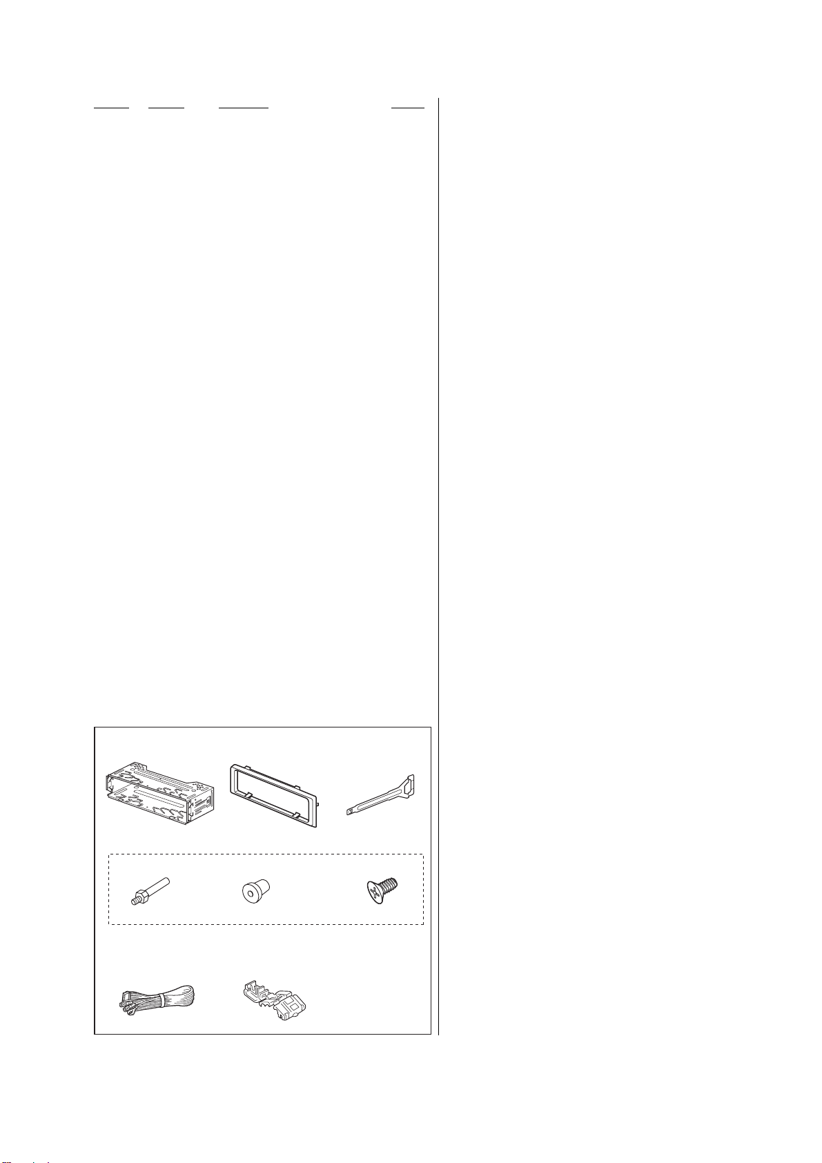
Ref. No. Part No. Description Remark
MISCELLANEOUS
***************
61-829-847-11 CABLE, FLAT (FFC) 26P
81-792-194-61 CORD (WITH CONNECTOR) (POWER)
91-829-836-12 CORD, CONNECTION (VIDEO) (VIDEO OUT)
0 153 8-820-207-12 OPTICAL PICK-UP (KSS1000E/K1RP)
154 A-1075-645-A CHASSIS (OP) SUB ASSY (including M901)
F901 1-532-877-11 FUSE (BLADE TYPE) (AUTO FUSE) 10A
M902 A-3372-447-A MOTOR ASSY, SL (SLED)
M903 A-1075-643-A MOTOR ASSY, LE (LOADING)
SW4 1-571-099-11 SWITCH (1 KEY) (LIMIT)
*************************************************************
ACCESSORIES
************
1-479-077-82 REMOTE COMMANDER (RM-X158)
2-548-729-01 LID, BATTERY CASE (for RM-X158)
2-582-332-21 MANUAL, INSTRUCTION (ENGLISH,
SIMPLIFIED CHINESE,ARABIC) (E)
2-582-333-21 MANUAL, INSTRUCTION, INSTALL (ENGLISH,
SIMPLIFIED CHINESE,ARABIC) (E)
2-596-986-11 MANUAL, INSTRUCTION (THAI) (E)
CDX-V3800
Ver. 1.2
2-664-618-11 MANUAL, INSTRUCTION
2-664-619-11 MANUAL, INSTRUCTION, INSTALL (ENGLISH,
X-3385-071-1 CASE ASSY (for FRONT PANEL)
*************************************************************
PARTS FOR INSTALLATION AND CONNECTIONS
***************************************
301 X-3382-647-1 FRAME ASSY, FITTING
302 3-261-542-02 COLLAR
303 3-246-471-01 KEY (FRAME)
304 X-3381-154-1 SCREW ASSY (BS4), FITTING
305 3-349-410-11 BUSHING
306 1-792-194-61 CORD (WITH CONNECTOR) (POWER)
307 1-562-593-11 CONNECTOR (CL-2218T)
301
302
(SIMPLIFIED CHINESE) (CHINESE)
SIMPLIFIED CHINESE,ARABIC) (CHINESE)
303
× 2
304
305
306 307
× 4
21
Page 66

CDX-V3800
REVISION HISTORY
Clicking the version allows you to jump to the revised page.
Also, clicking the version at the upper on the revised page allows you to jump to the next revised page.
Ver. Date Description of Revision
1.0 2005.01 New
1.1 2005.05 Production country change. (ENG-05004)
1.2 2005.11 Chinese model addition.
1.3 2006.05 Correction of RF level. (SPM-06010)
22
 Loading...