

Sony CDXM-8815-X Service manual
CDX-M8810/M8815X
SERVICE MANUAL
Ver. 1.0 2005.01
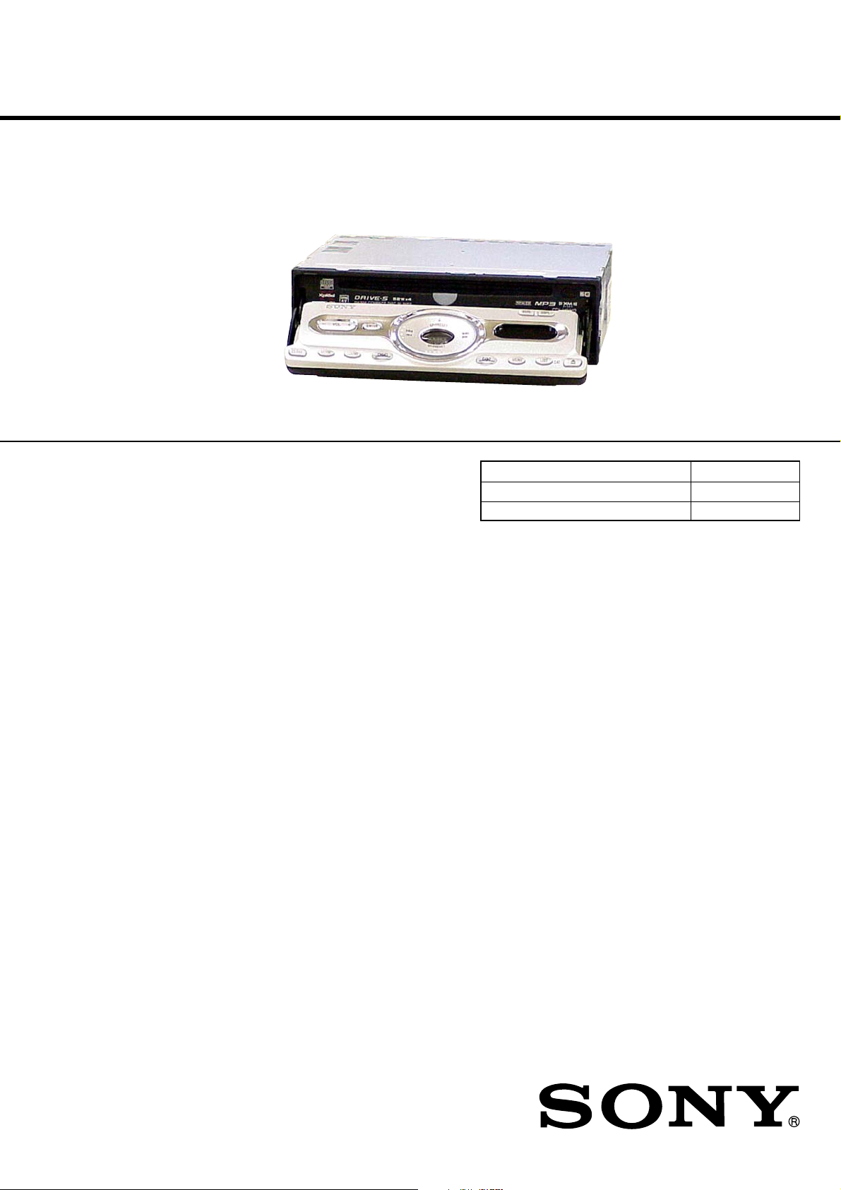
Photo: CDX-M8810
• The tuner and CD sections have no adjustments.
SPECIFICATIONS
AUDIO POWER SPECIFICATIONS (US MODEL)
POWER OUTPUT AND TOTAL HARMONIC DISTORTION
23.2 watts per channel minimum continuous average power into
4 ohms, 4 channels driven from 20 Hz to 20 kHz with no more
than 5% total harmonic distortion.
CD player section
Signal-to-noise ratio 120 dB
Frequency response 10 – 20,000 Hz
Wow and flutter Below measurable limit
Tuner section
FM
Tuning range 87.5 – 107.9 MHz
Antenna terminal External antenna connector
Intermediate frequency 10.7 MHz/450 kHz
Usable sensitivity 9 dBf
Selectivity 75 dB at 400 kHz
Signal-to-noise ratio 67 dB (stereo),
69 dB (mono)
Harmonic distortion at 1 kHz
0.5% (stereo),
0.3% (mono)
Separation 35 dB at 1 kHz
Frequency response 30 – 15,000 Hz
AM
Tuning range 530 – 1,710 kHz
Antenna terminal External antenna connector
Intermediate frequency 10.7 MHz/450 kHz
Sensitivity 30 µV
US Model
Canadian Model
Model Name Using Similar Mechanism CDX-F7715X
CD Drive Mechanism Type MG-611TS-186//K
Optical Pick-up Name KSS1000E
Power amplifier section
Outputs Speaker outputs (sure seal connectors)
Speaker impedance 4 – 8 ohms
Maximum power output 52 W × 4 (at 4 ohms)
General
Outputs Audio output terminal (front/rear)
Subwoofer output terminal (mono)
Power antenna relay control terminal
Power amplifier control terminal
Inputs Telephone ATT control terminal
Illumination control terminal
BUS control input terminal
BUS audio input or AUX IN terminal
Remote controller input terminal
Antenna input terminal
Tone controls Bass ±10 dB at 62 Hz
Treble ±10 dB at 16 kHz
Loudness +8 dB at 100 Hz
+2 dB at 10 kHz
Power requirements 12 V DC car battery
(negative ground)
Dimensions Approx. 178 × 50 × 184 mm
(7 1/8 × 2 × 7 1/4 in.) (w/h/d)
Mounting dimensions Approx. 182 × 53 × 162 mm
(7 1/4 × 2 1/8 × 6 1/2 in.) (w/h/d)
Mass Approx. 1.7 kg (3 lb. 12 oz.)
Supplied accessories Parts for installation and connections (1 set)
Card remote commander: RM-X143A
Note
This unit cannot be connected to a digital preamplifier or an equalizer.
Design and specifications are subject to change without
notice.
9-879-383-01
2005A04-1
© 2005.01
FM/AM COMPACT DISC PLAYER
Sony Corporation
e Vehicle Company
Published by Sony Engineering Corporation
1
CDX-M8810/M8815X
SERVICE NOTES
NOTES ON HANDLING THE OPTICAL PICK-UP BLOCK
OR BASE UNIT
The laser diode in the optical pick-up block may suffer electrostatic
breakdown because of the potential difference generated by the
charged electrostatic load, etc. on clothing and the human body.
During repair, pay attention to electrostatic breakdown and also use
the procedure in the printed matter which is included in the repair
parts.
The flexible board is easily damaged and should be handled with
care.
NOTES ON LASER DIODE EMISSION CHECK
The laser beam on this model is concentrated so as to be focused on
the disc reflective surface by the objective lens in the optical pickup block. Therefore, when checking the laser diode emission, observe from more than 30 cm away from the objective lens.
Notes on Chip Component Replacement
• Never reuse a disconnected chip component.
• Notice that the minus side of a tantalum capacitor may be dam-
aged by heat.
CAUTION
Use of controls or adjustments or performance of procedures
other than those specified herein may result in hazardous
radiation exposure.
If the optical pick-up block is defective, please replace the whole
optical pick-up block.
Never turn the semi-fixed resistor located at the side of optical
pick-up block.
optical pick-up
semi-fixed resistor
TEST DISCS
This set can playback CD-R and CD-ROM discs. The following
test discs should be used to check the capability:
CD-R test disc TCD-R082LMT (Part No. J-2502-063-1)
CD-RW test disc TCD-W082L (Part No. J-2502-063-2)
SAFETY-RELATED COMPONENT WARNING!!
COMPONENTS IDENTIFIED BY MARK 0 OR DOTTED LINE
WITH MARK 0 ON THE SCHEMATIC DIAGRAMS AND IN
THE PARTS LIST ARE CRITICAL TO SAFE OPERATION.
REPLACE THESE COMPONENTS WITH SONY P ARTS WHOSE
PART NUMBERS APPEAR AS SHOWN IN THIS MANUAL OR
IN SUPPLEMENTS PUBLISHED BY SONY.
2
ATTENTION AU COMPOSANT AYANT RAPPORT
À LA SÉCURITÉ!!
LES COMPOSANTS IDENTIFIÉS P AR UNE MARQUE 0 SUR LES
DIAGRAMMES SCHÉMATIQUES ET LA LISTE DES PIÈCES
SONT CRITIQUES POUR LA SÉCURITÉ DE FONCTIONNEMENT .
NE REMPLACER CES COMPOSANTS QUE PAR DES PIÈCES
SONY DONT LES NUMÉROS SONT DONNÉS DANS CE MANUEL
OU DANS LES SUPPLÉMENTS PUBLIÉS PAR SONY.
CDX-M8810/M8815X
D
• CD Playback:
You can play CD-DA (also containing CD TEXT*1), CD-R/CDRW (MP3 files also containing Multi Session and ATRAC CD
(ATRAC3 and ATRAC3plus format).
Type of discs Label on the disc
CD-DA
MP3
ATRAC CD
*1 A CD TEXT disc is a CD-D A that includes information such as
disc, artist and track name.
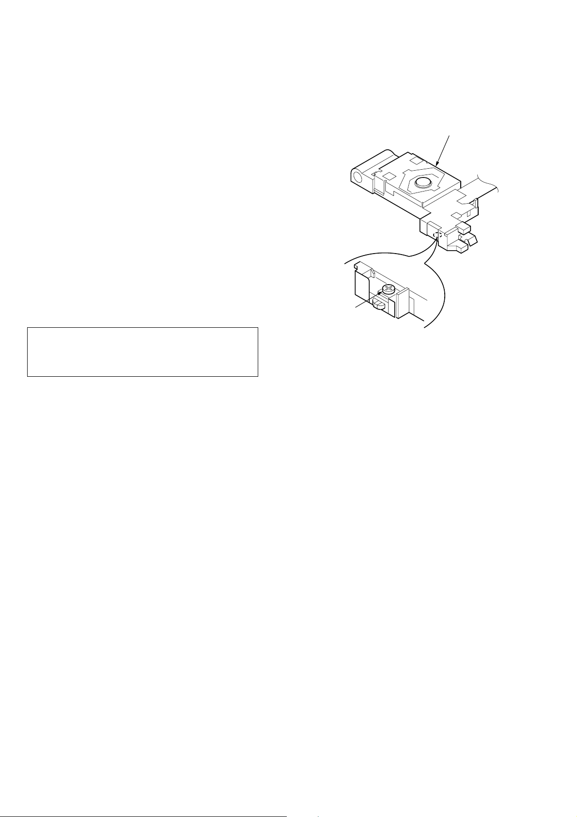
EXTENSION CABLE AND SERVICE POSITION
When repairing or servicing this set, connect the jig (extension cable)
as shown below.
z UNLEADED SOLDER
Boards requiring use of unleaded solder are printed with the lead
free mark (LF) indicating the solder contains no lead.
(Caution: Some printed circuit boards may not come printed with
the lead free mark due to their particular size)
: LEAD FREE MARK
Unleaded solder has the following characteristics.
• Unleaded solder melts at a temperature about 40 °C higher
than ordinary solder.
Ordinary soldering irons can be used but the iron tip has to be
applied to the solder joint for a slightly longer time.
Soldering irons using a temperature regulator should be set to
about 350 °C.
Caution: The printed pattern (copper foil) may peel away if
the heated tip is applied for too long, so be careful!
• Strong viscosity
Unleaded solder is more viscou-s (sticky, less prone to flow)
than ordinary solder so use caution not to let solder bridges
occur such as on IC pins, etc.
• Usable with ordinary solder
It is best to use only unleaded solder but unleaded solder may
also be added to ordinary solder.
• Connect the MAIN board (CNP301) and the SER VO board (CN2)
with the extension cable (Part No. J-2502-076-1).
MAIN BOARD
CNP301
J-2502-076-1
SERVO BOAR
CN2
3
CDX-M8810/M8815X
NOTE FOR THE OPENING OF THE FRONT PANEL
In this set, the front panel is lowered to below the bottom face when
it is opened.
When servicing the set, place it on a stand having a height of about
2 cm.
stand
TABLE OF CONTENTS
1. GENERAL
Location of Controls................................................................5
Connections ............................................................................. 5
2. DISASSEMBLY
2-1. Screw (Panel) ......................................................................8
2-2. CD Mechanism Block ......................................................... 8
2-3. Front Panel Assy .................................................................9
2-4. Sub Panel (CD) Assy........................................................... 9
2-5. Driving Section (DB-A04) ................................................ 10
2-6. Follow Move (A) Service Assy,
Driving (A) Service Assy ..................................................10
2-7. Main Board ....................................................................... 11
2-8. Chassis (T) Sub Assy ........................................................11
2-9. Roller Arm Assy ................................................................ 12
2-10. Chassis (OP) Assy.............................................................12
2-11. Optical Pick-up ................................................................. 13
2-12. SL Motor Assy (M902) ..................................................... 13
2-13. LE Motor Assy (M903)..................................................... 14
2-14. Servo Board....................................................................... 14
3. DIAGRAMS
3-1. Block Diagram –CD Section–........................................... 15
3-2. Block Diagram –Main Section–........................................16
3-3. Block Diagram –Display Section–....................................17
3-4. Circuit Boards Location .................................................... 18
3-5. Printed Wiring Boards –CD Mechanism Section–............ 19
3-6. Schematic Diagram –CD Mechanism Section (1/2)– ....... 20
3-7. Schematic Diagram –CD Mechanism Section (2/2)– ....... 21
3-8. Printed Wiring Boards –Main Section– ............................ 22
3-9. Schematic Diagram –Main Section (1/4)– ........................ 24
3-10. Schematic Diagram –Main Section (2/4)– ........................ 25
3-11. Schematic Diagram –Main Section (3/4)– ........................ 26
3-12. Schematic Diagram –Main Section (4/4)– ........................ 27
3-13. Printed Wiring Board –Sub Section– ................................28
3-14. Printed Wiring Board –Display Section– .......................... 29
3-15. Schematic Diagram –Display Section–............................. 30
4. EXPLODED VIEWS
4-1. Chassis Section ................................................................. 43
4-2. Main Board Section .......................................................... 44
4-3. Front Panel Section ...........................................................45
4-4. CD Mechanism Section (1) ............................................... 46
4-5. CD Mechanism Section (2) ............................................... 47
4-6. CD Mechanism Section (3) ............................................... 48
4-7. CD Mechanism Section (4) ............................................... 49
5. ELECTRICAL PARTS LIST......................................... 50
4
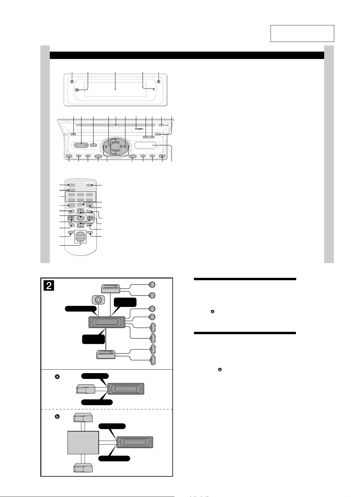
Location of controls and basic operations
w
w
w
w
w
q
q
qjq
q
Main display side
12 534
Operation side
67 8 9 qa04qsqd 2 qf
OFF ATT
VOL
ENTER
SOUND
MODE
CLOSE
h
g
DSO
l
k
Card remote commander
RM-X143A
OPEN/CLOSE
SCRL
qs
qd
wg
w;
wa
qa
ql
qj
6
DSPL
REP SHUF
1
253
BBE MP PAUSE
4
MODE
EQ7 DSO
U
+
DISC
EN
M
SOURCE
–
SEEK
S
O
U
–
N
DISC
D
+
VOL
–
wh
6
qh
qk
C
A
T
L
IS
T
+
SEEK
ws
TER
9
N
E
8
AT TOFF
qf
7
6
SCRL DSPL
SOURCE
CDX-M8815X/M8810
EQ7
;
Refer to the pages listed for details. The
corresponding buttons on the card remote
commander control the same functions as those
on the unit.
A Open button 5
To open the front panel.
B Receptor
To receive signals from the card remote
commander or wireless rotary commander.
C Main display window
D RESET button 4
E Image button 2
To s e lect the display image.
Space Producer mode t Wall paper mode
1-3 t Spectrum analyzer mode 1-5 t
Movie mode 1-2 t normal play/reception
mode
F OFF button
To p owe r off/stop the source.
LIST CATMENU
s
a
SECTION 1
GENERAL
f
d
G VOL (volume) +/– button
To a d just volume.
H ENTER button
To c o mplete a setting.
1
I GP*
/PRESET, M/m +/– buttons
To s e l e ct preset stat ions/skip groups (press);
skip groups continuously (press and hold).
J Disc slot 5
To i n sert the disc.
K SOURCE button
To p owe r on/change the source (Radio/CD/
2
MD*
/AUX*3).
L SCRL (scroll) button 8
To s c roll the display item.
M DSPL (display) button 8, 10
To c h ange display items.
N ATT (attenuate) button
To attenuate the sound. To cancel, press
again.
O CLOSE button 5
To c l ose the front panel.
P MODE button 8, 12
To select the radio band (FM/AM)/sele ct the
4
unit*
.
Q SOUND button 9
To s e lect sound items.
R DSO button 2
To select the DSO mode (1, 2, 3 or OFF).
The larger the number, the more enhanced
the effect.
S .m/M>, </, +/– buttons
Radio:
To tune in stations automatically (press); find
a station manually (press an d hold).
CD:
To s k ip tracks (press); skip tracks
continuously (press, t hen press again within
about 1 second and hold); fast- fo rw ard/
reverse a track (press and hold).
T EQ7 (equalizer) button
To select an equalizer type (Xplod, VOCAL,
CLUB, JAZZ, NEW A GE, ROCK, CUSTOM
or OFF).
U MENU button
To e n ter menu.
To l i st up.
5
button 9, 12
V LIST/CAT*
CDX-M8810/M8815X
This section is extracted
from instruction manual.
W Z (eject) button 5
To eject the disc.
X Sub display window
The following buttons on the card remote
commander have also different buttons/functions
from the unit.
y Number buttons
Radio:
To receive stored stations (press); store
stations (press and hold).
2
:
CD/MD*
(1): REP 8
(2): SHUF 8
(5): BBE MP*
To activate the BBE MP function, set “BBE
MP-on.” To cancel, set “BBE MP-off.”
(6): PA U SE *
To pause playback. To cancel, press again.
z OPEN/CLOSE button 5
To open/close the front panel.
*1
When an MP3/ATRAC CD is played an d a ch an g er
is not c
operati
*2
When an MD changer is connected.
*3
When an optional Sony portable devi ce is
connected.
*4
When a CD/MD changer is connected.
*5
When the XM tuner is connected.
*6
When playing back on this unit
Note
If the unit is turned off and the display disappears, it
cannot be operated with the card remote commander
unless
inserted to activate the unit first.
Tip
For details on how to replace the battery, see
“Replacing the lithium battery of the card remote
commander” on page 14.
6
3
6
onnected. If the changer is connected, the
on is different, see page 12.
.
(SOURCE)
on the unit is pressed, or a disc is
7
• Connections
A
SUB OUT (MONO)
B
Source selector*
Sélecteur de source*
AUDIO OUT
REAR
BUS AUDIO IN
BUS CONTROL IN
XA-C30
AUDIO OUT
BUS AUDIO IN
FRONT
Connection example (2)
Notes
(2-A)
• Be sure to connect the ground lead before connecting the
amplifi er.
• The alarm will only sound if the built-in amplifi er is used.
Tip
(2-B-
For connecting two or more CD/MD changers, the source
selector XA-C30 (optional) is necessary.
)
Exemple de raccordement (2)
Remarques
• Raccordez d’abord le câble de mise à la masse a
• L’alarme est émise uniquement lorsque l’amplifi cateur intégré
Conseil
Dans le cas du raccordement de deux changeurs de CD/MD ou
plus, le sélecteur de source XA-C30 (en option) est requis.
(2-A)
raccorder l’amplifi cateur.
est utilisé.
(2-B-
)
vant de
BUS CONTROL IN
*
not supplied
non fourni
5
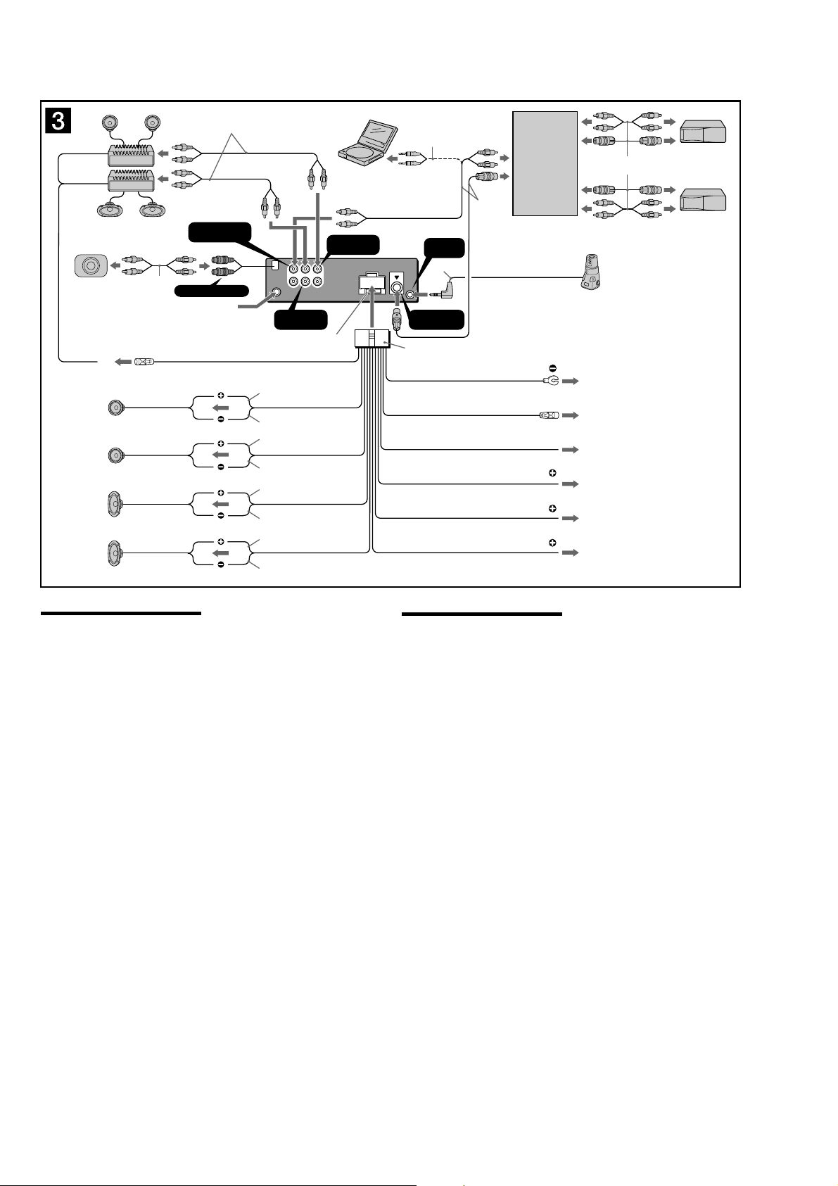
CDX-M8810/M8815X
1
*
3
*
4
*
*
5
Source selector
(not supplied)
Sélecteur de source
(non fourni)
XA-C30
Supplied with the CD/MD changer
Fourni avec le changeur de CD/MD
1
*
SUB OUT (MONO
Left
Gauche
Right
Droit
Left
Gauche
Right
Droit
from car antenna
à partir de l’antenne de la voiture
AMP REM
3
Max. supply current 0.3 A
Courant max. fourni 0,3 A
Connection diagram (3)
1 To a metal surface of the car
First connect the black ground lead, then connect the
orange/white striped, yellow, and red power input leads.
2 To the power antenna control lead or power
supply lead of antenna booster amplifi er
Notes
• It is not necessary to connect this lead if there is no power
antenna or antenna booster, or with a manually-operated
telescopic antenna.
• When your car has a built-in FM/AM antenna in the rear/
side glass, see “Notes on the control and power supply
leads.”
3 To AMP REMOTE IN of an optional power
amplifi er
This connection is only for amplifi ers. Connecting any other
system may damage the unit.
4 To the interface cable of a car telephone
5 To a car’s illumination signal
Be sure to connect the black ground lead to a metal surface
of the car fi rst.
6 To the +12 V power terminal which is
energized in the accessory position of the
ignition key switch
Notes
• If there is no accessory position, connect to the +12 V
power (battery) terminal which is energized at all times.
Be sure to connect the black ground lead to a metal
surface of the car fi rst.
• When your car has a built-in FM/AM antenna in the rear/
side glass, see “Notes on the control and power supply
leads.”
7 To the +12 V power terminal which is
energized at all times
Be sure to connect the black ground lead to a metal surface
of the car fi rst.
BUS AUDIO IN
/AUX IN
2
*
)
AUDIO OUT
REAR
Fuse (10 A)
Blue/white striped
Rayé bleu/blanc
Notes on the control and power supply leads
• The power antenna control lead (blue) supplies +12 V DC
when you turn on the tuner.
• When your car has built-in FM/AM antenna in the rear/side
glass, connect the power antenna control lead (blue) or the
accessory power input lead (red) to the power terminal of the
existing antenna booster. For details, consult your dealer.
• A power antenna without a relay box cannot be used with this
unit.
Memory hold connection
When the yellow power input lead is connected, power will
always be supplied to the memory circuit even when the ignition
switch is turned off.
Notes on speaker connection
• Before connecting the speakers, turn the unit off.
• Use speakers with an impedance of 4 to 8 ohms, and with
adequate power handling capacities to avoid its damage.
• Do not connect the speaker terminals to the car chassis, or
connect the terminals of the right speakers with those of the
left speaker.
• Do not connect the ground lead of this unit to the negative (–)
terminal of the speaker.
• Do not attempt to connect the speakers in parallel.
• Connect only passive speakers. Connecting active speakers
(with built-in amplifi ers) to the speaker terminals may damage
the unit.
• To avoid a malfunction, do not use the built-in speaker leads
installed in your car if the unit shares a common negative (–)
lead for the right and left speakers.
• Do not connect the unit’s speaker leads to each other.
Note on connection
If speaker and amplifi er are not connected correctly, “Failure”
appears in the display. In this case, make sure the speaker and
amplifi er are connected correctly.
Fusible (10 A)
White
Blanc
White/black striped
Rayé blanc/noir
Gray
Gris
Gray/black striped
Rayé gris/noir
Green
Vert
Green/black striped
Rayé vert/noir
Purple
Mauve
Purple/black striped
Rayé mauve/noir
AUDIO OUT
FRONT
REMOTE
IN
6
*
BUS
CONTROL IN
2
Black
Noir
Blue
Bleu
Light blue
Bleu ciel
Orange/white striped
Rayé orange/blanc
Red
Rouge
Yellow
Jaune
Max. supply current 0.1 A
Courant max. fourni 0,1 A
ANT REM
AT T
ILLUMINATION
Schéma de raccordement (3)
1 À un point métallique de la voiture
Branchez d’abord le fi l de masse noir et, ensuite, les fi ls
d’entrée d’alimentation rayé orange/blanc, jaune, et rouge.
2 Vers le câble de commande d’antenne
électrique ou le câble d’alimentation de
l’amplifi cateur d’antenne
Remarques
• Il n’est pas nécessaire de raccorder ce câble s’il n'y a pas
d’antenne électrique ni d’amplifi cateur d’antenne, ou avec
une antenne télescopique manuelle.
• Si votre voiture est équipée d’une antenne FM/AM
intégrée dans la vitre arrière/latérale, voir « Remarques
sur les câbles de commande et d’alimentation ».
3 Au niveau de AMP REMOTE IN de
l’amplifi cateur de puissance en option
Ce raccordement s’applique uniquement aux amplifi cateurs.
Le branchement de tout autre système risque
d’endommager l’appareil.
4 Vers le cordon de liaison d’un téléphone de
voiture
5 Vers le connecteur du signal d’éclairage de
la voiture
Raccordez d’abord le câble de mise à la masse noir à un
point métallique du véhicule.
6 À la borne +12 V qui est alimentée quand la
clé de contact est sur la position accessoires
Remarques
• S’il n’y a pas de position accessoires, raccordez la borne
d’alimentation (batterie) +12 V qui est alimentée en
permanence. Raccordez d’abord le câble de mise à la
masse noir à un point métallique du véhicule.
• Si votre voiture est équipée d’une antenne FM/AM
intégrée dans la vitre arrière/latérale, voir « Remarques
sur les câbles de commande et d’alimentation ».
7 À la borne +12 V qui est alimentée en
permanence
Raccordez d’abord le câble de mise à la masse noir à un
point métallique du véhicule.
1
*
RCA pin cord (not supplied)
2
*
Be sure to match the color-
coded cord for audio to the
appropriate jacks from the
unit. If you connect an optional
CD/MD changer, you cannot
use AUX IN terminal.
3
*
Auxiliary optional equipment
such as portable DVD player
(not supplied)
4
*
Supplied with the auxiliary
equipment
5
*
Supplied with XA-C30
6
*
Insert with the cord upwards.
1
*
Cordon à broche RCA (non
1
2
4
5
fourni)
2
*
Veillez à faire correspondre
le code de couleur du cordon
audio à celui des fi ches
correspondantes de l’appareil.
Si vous raccordez un changeur
de CD/MD en option, vous ne
pouvez pas utiliser la borne
AUX IN.
3
*
Appareil auxiliaire en option,
par exemple un lecteur de DVD
table (non fourni)
por
4
*
Fourni avec l’appareil auxiliaire
5
*
Fourni avec le XA-C30
6
*
Insérez avec le câble vers le
bas.
6
7
Remarques sur les câbles de commande et d’alimentation
• Le câble de commande d’antenne électrique (bleu) fournit une
alimentation de + 12 V CC lorsque vous mettez la radio sous
tension.
• Lorsque votre voiture est équipée d’une antenne FM/AM
intégrée dans la vitre arrière/latérale, raccordez le câble de
commande d’antenne
des accessoires (rouge) à la borne d’alimentation de
l’amplifi cateur d’antenne
votre détaillant.
• Une antenne électrique sans boîtier de relais ne peut pas être
utilisée avec cet appareil.
Raccordement pour la conservation de la mémoire
Lorsque le câble d’entrée d’alimentation jaune est raccordé, le
circuit de la mémoire est alimenté en permanence même si la clé
de contact est sur la position d’arrêt.
Remarques sur le raccordement des haut-parleurs
• Avant de raccorder les haut-parleurs, mettez l’appareil hors
tension.
• Utilisez des haut-parleurs ayant une impédance de 4 à 8 ohms
avec une capacité électrique adéquate pour éviter de les
endommager.
• Ne raccordez pas les bornes du système de haut-parleurs au
châssis de la voiture et ne raccordez pas les bornes des hautparleurs droit à celles du haut-parleur gauche.
• Ne raccordez pas le câble de mise à la masse de cet appareil
à la borne négative (–) du haut-parleur.
• N’essayez pas de raccorder les haut-parleurs en parallèle.
• Raccordez uniquement des haut-parleurs passifs. Le
raccordement de haut-parleurs actifs (avec amplifi cateurs intégrés)
aux bornes des haut-parleurs peut endommager l’appareil.
• Pour éviter tout dysfonctionnement, n’utilisez pas les câbles
des haut-parleurs intégrés installés dans votre voiture si
l’appareil partage un câble négatif commun (–) pour les hautparleurs droit et gauche.
• Ne raccordez pas entre eux les cordons des haut-parleurs de
l’appareil.
Remarque sur le raccordement
Si les haut-parleurs et l’amplifi cateur ne sont pas raccordés
correctement, le message « Failure » s’affi che. Dans ce cas,
assurez-v
raccordés.
électrique
(bleu) ou l’entrée d’alimentation
existant. Pour plus de détails, consultez
ous que les haut-parleurs et l’amplifi cateur sont bien
6
SECTION 2
DISASSEMBLY
Note : This set can be disassemble according to the following sequence.
SET
2-1. SCREW (PANEL)
(Page 8)
2-2. CD MECHANISM BLOCK
(Page 8)
CDX-M8810/M8815X
2-3. FRONT PANEL ASSY
(Page 9)
2-4. SUB PANEL (CD) ASSY
(Page 9)
2-5. DRIVING SECTION
(DB-A04)
(Page 10)
2-7. MAIN BOARD
(Page 11)
2-11. OPTICAL PICK-UP
2-6. FOLLOW MOVE (A) SERVICE ASSY,
DRIVING (A) SERVICE ASSY
(Page 10)
2-8. CHASSIS (T) SUB ASSY
(Page 11)
2-9. ROLLER ARM ASSY
(Page 12)
2-10. CHASSIS (OP) ASSY
(Page 12)
2-12. SL MOTOR ASSY (M902)
(Page 13)
(Page 13)
2-14. SERVO BOARD
(Page 14)
2-13. LE MOTOR ASSY (M903)
(Page 14)
7
CDX-M8810/M8815X
Note : Follow the disassembly procedure in the numerical order given.
2-1. SCREW (PANEL)
2
screw
(panel)
front panel assy
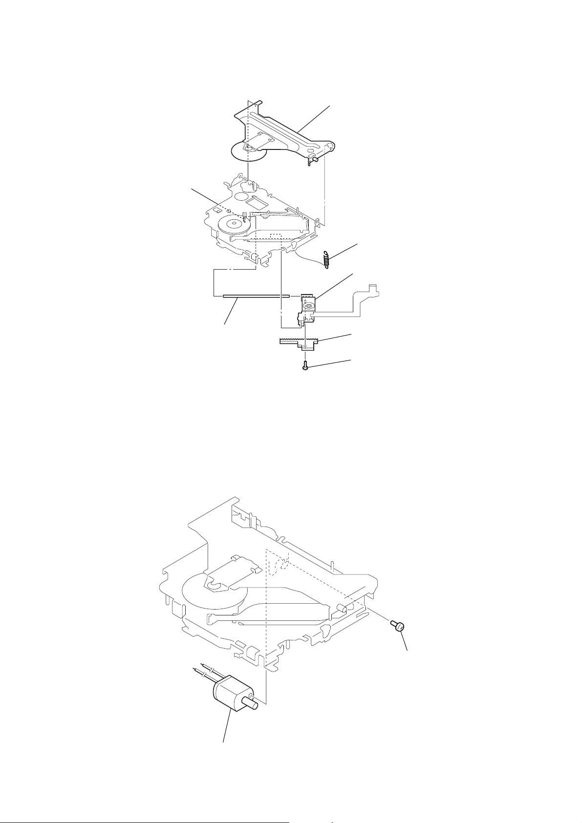
2-2. CD MECHANISM BLOCK
6
CD mechanism block
2
screw
(+PTT 2.6
x
8
6)
bracket (CD)
4
1
screw
(panel)
7
two
screws
(+PTT 2.6
x
6)
1
two
screws
(+PTT 2.6
x
6)
3
screw
5
CNP301
(+PTT 2.6
x
6)
8
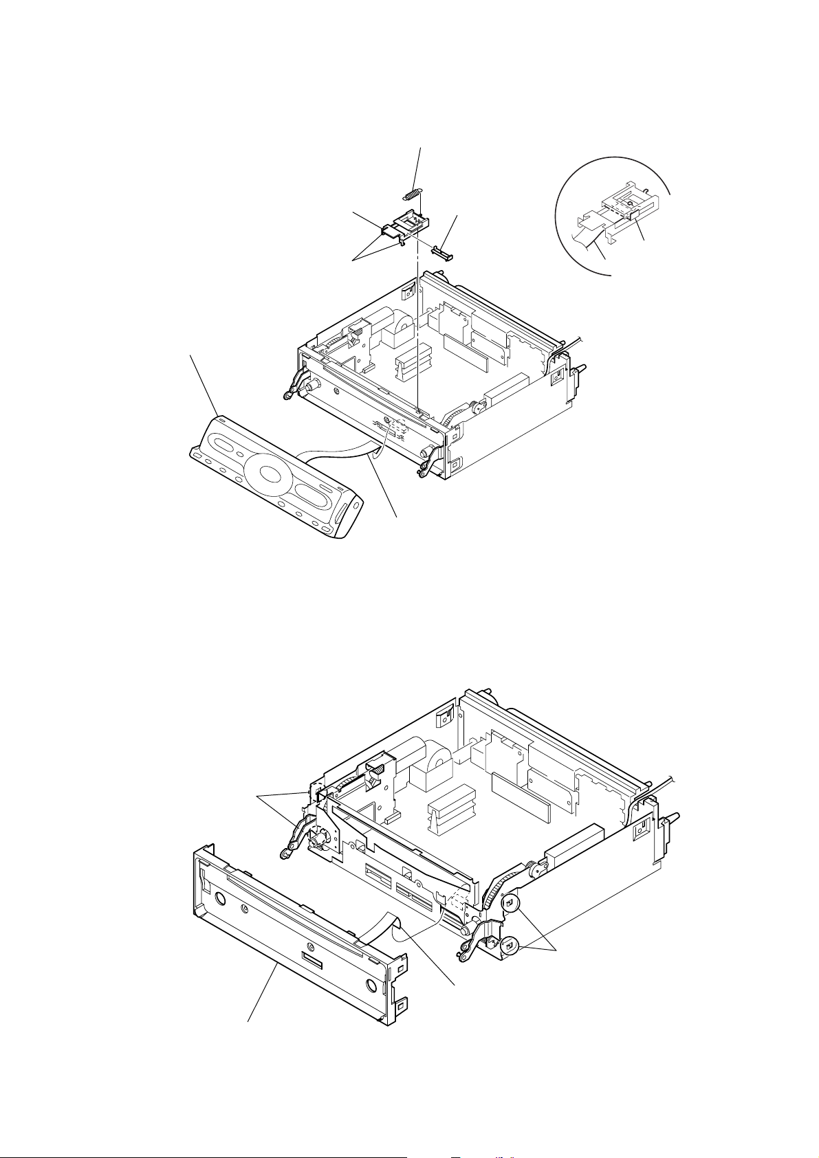
2-3. FRONT PANEL ASSY
5
front panel assy
3
cover (FPC)
two claws
1
tension spring (FPC)
2
slider (FPC)
CDX-M8810/M8815X
slider (FPC)
flexible board
Note: When installing
the flexible board,
make the board slack
as illustrated.
2-4. SUB PANEL (CD) ASSY
two claws
4
CNP909
2
sub panel (CD) assy
1
CN506
two claws
9
CDX-M8810/M8815X
)
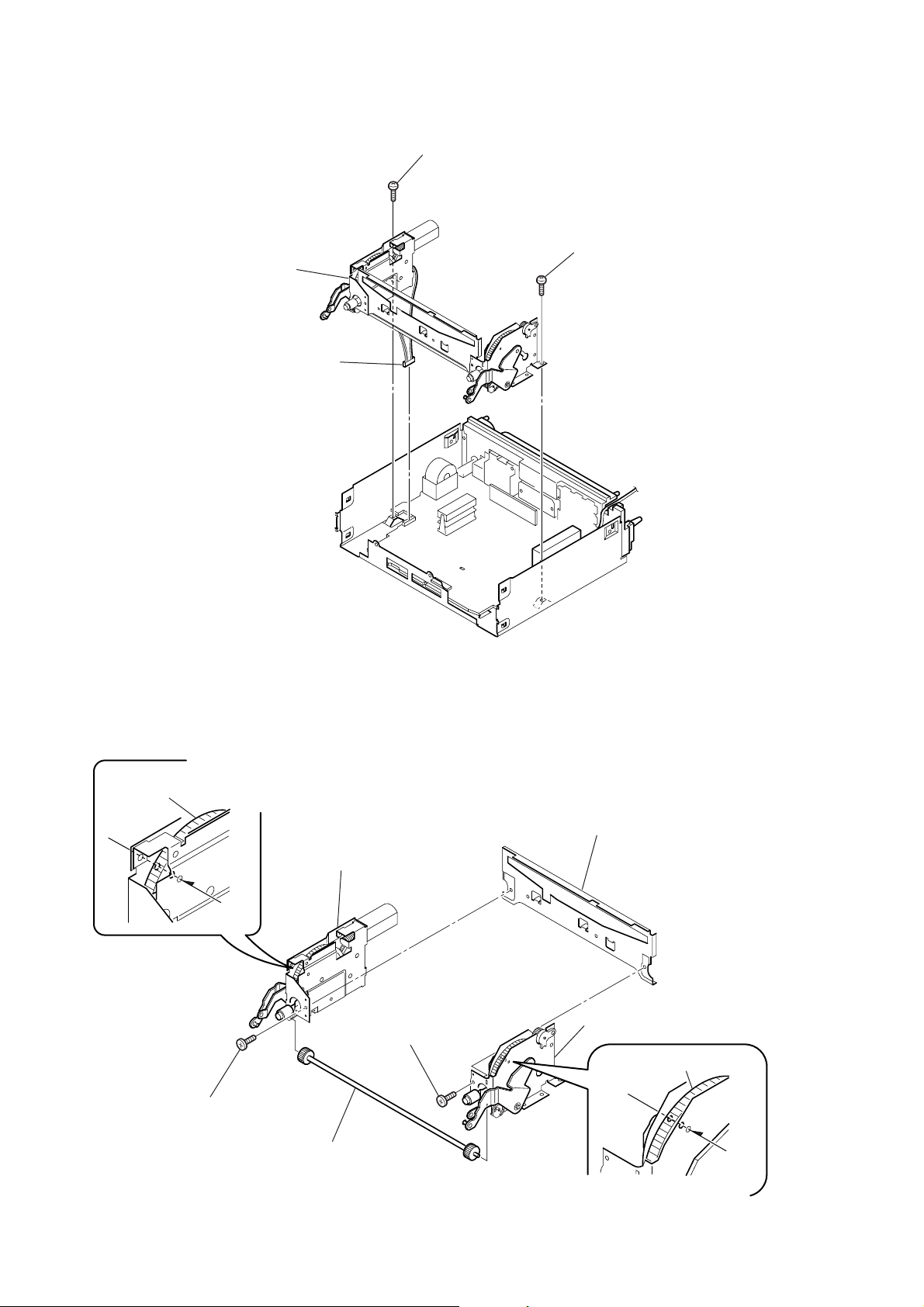
2-5. DRIVING SECTION (DB-A04)
4
driving section (DB-A04)
1
CN902
2
screw
(+PTT 2.6
x
6)
3
screw
(+PTT 2.6
x
6
2-6. FOLLOW MOVE (A) SERVICE ASSY, DRIVING (A) SERVICE ASSY
To install the assembly, turn the can (LA) and
cam (LA)
align the detent with the holes A.
5
driving (A) service assy
A
1
screw
4
screw
(+STP 2.6
x
(+STP 2.6
6)
3
drive shaft assy
x
6)
6
plate (joint)
2
follow move (A) service assy
cam (RA)
B
10
To install the assembly,
turn the can (RA) and align
the detent with the holes B.
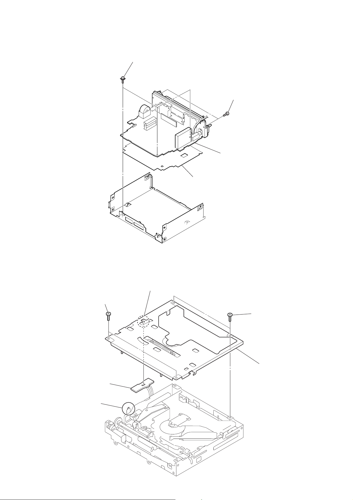
2-7. MAIN BOARD
)
1
three ground point
(+PTT 2.6
x
CDX-M8810/M8815X
screws
6)
2
two
screws
4
insulating sheet
(+PTT 2.6
3
MAIN board
x
8
2-8. CHASSIS (T) SUB ASSY
2
two
screws
x
(+P 1.7
5
SENSOR board
3
claw
2.2)
4
claw
1
two
screws
x
(+P 1.7
6
2.2)
chassis (T) sub assy
11
CDX-M8810/M8815X
2-9. ROLLER ARM ASSY
4
gear (RA1)
1
spring (RAL)
3
washer (1.1-2.5)
5
roller arm assy
2
spring (RAR)
2-10. CHASSIS (OP) ASSY
0
coil spring (damper)
4
washer
5
gear (LE1)
lever (D)
6
8
qa
chassis (OP) assy
1
CN1 (16P)
9
two coil springs (damper)
7
slider (R)
12
2
Remove the six solderings.
3
tension coil spring (KF60)
2-11. OPTICAL PICK-UP
)
5
claw
2
chucking arm sub assy
1
tension coil spring (CHKG
7
optical pick-up
CDX-M8810/M8815X
2-12. SL MOTOR ASSY (M902)
6
main shaft
4
rack (SL)
3
screw
(+B 1.4
x
5)
2
SL motor assy (M902)
1
screw
(+P 1.4
x
1.8)
13
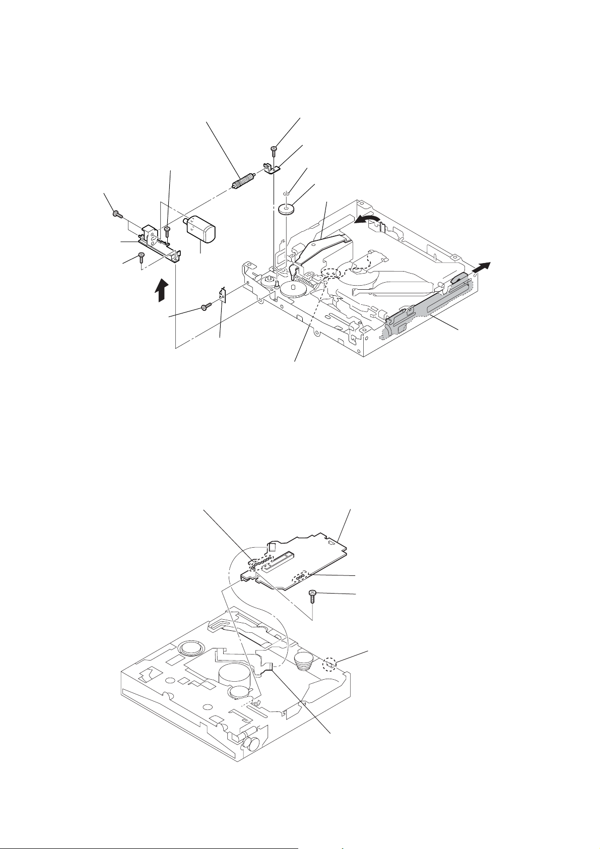
CDX-M8810/M8815X
2-13. LE MOTOR ASSY (M903)
qf
two toothed lock
(+M 1.4
bracket (LEM-N)
qs
screw
(+M 1.7
)
x
screws
2.5)
6
screw
(+P 1.7
x
qd
2.2)
qa
screw
(+M 1.7
0
gear (LE) assy
x
2.5)
qg
LE motor assy
(M903)
7
leaf spring (LE)
8
screw
(+M 1.7
9
2
x
bearing (LEB-N)
washer
gear (LE1)
3
lever (D)
2.5)
4
5
slider (R)
2-14. SERVO BOARD
1
Remove the eight solderings.
1
Remove the soldering.
6
SERVO board
2
Remove the three solderings.
4
toothed lock
(M 1.7)
5
claw
screw
14
3
CN1(16P)
SECTION 3
DIAGRAMS
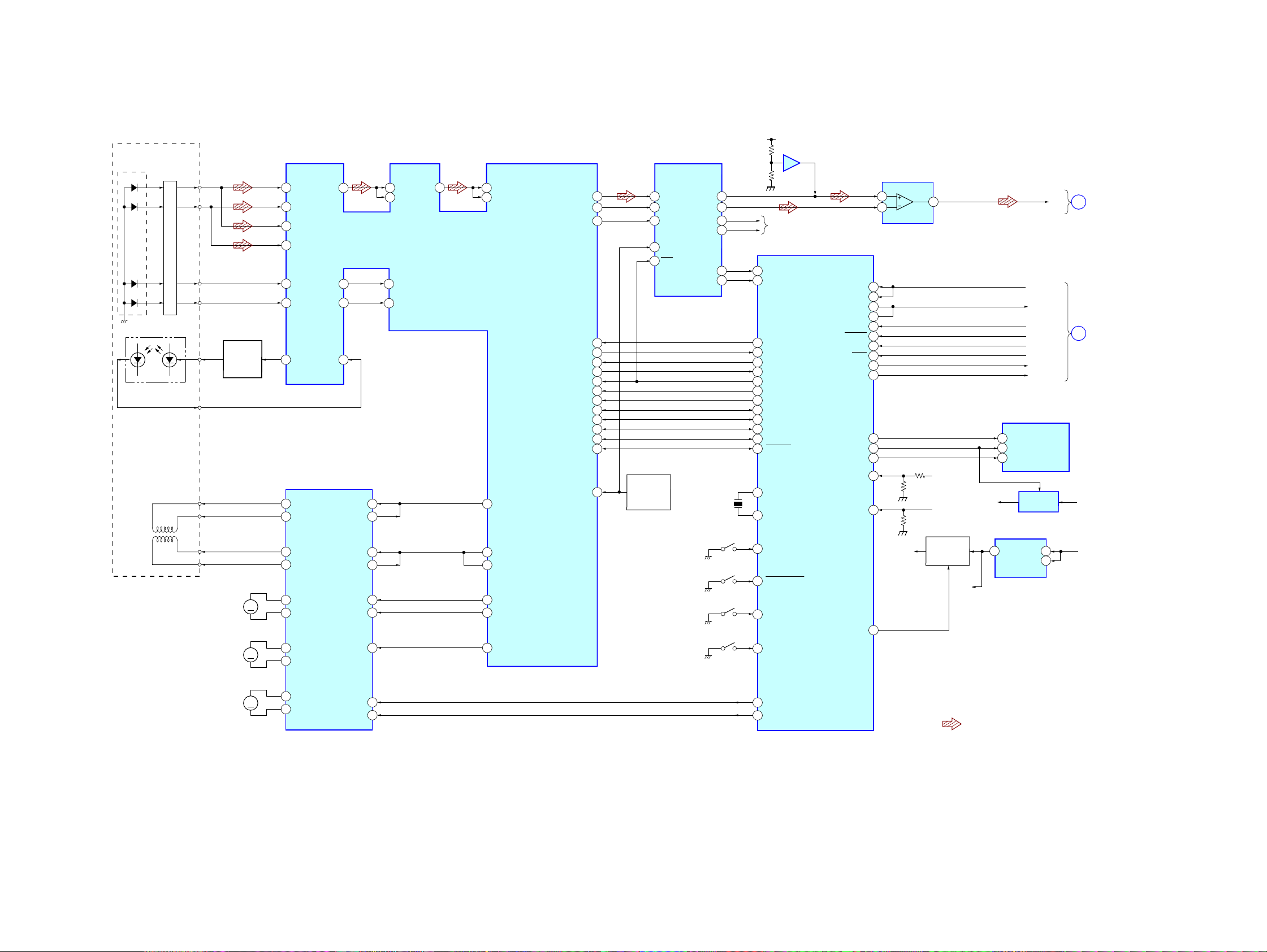
3-1. BLOCK DIAGRAM — CD SECTION —
DETECTOR
PD2
PD1
E
F
LASER DIODE
PICK-UP BLOCK
(KSS1000E)
2-AXIS DEVICE
(FOCUS)
(TRACKING)
PD LD
OPTICAL
PD2
PD1
I-V AMP
MON OUT
FCS+
FCS–
TRK+
TRK–
FPI2
96
FNI2
94
FPI1
97
FNI1
95
E
F
LD
AUTOMATIC
CONTROL
M902
(SLED)
M901
(SPINDLE)
POWER
Q1
M
M
99
98
91
FOCUS/TRACKING COIL DRIVE,
16
15
18
17
14
13
12
11
RFRP
TNI
TPI
LDO
SLED/SPINDLE/LOADING
MOTOR DRIVE
VO4–
VO4+
VO3–
VO3+
VO1+
VO1–
VO2+
VO2–
RFO
MDI
IC1
CDX-M8810/M8815X
AU+5V
R-CH
DAC ZDETL
22
DAC ZDETR
23
DEC XMUTE
37
DEC INT
30
DEC SSTBY
27
CD ZDET
15
CD XRST
14
CD XCCE
13
CD BUCK
12
CD BUS3
11
CD BUS2
10
CD BUS1
8
CD BUS0
7
CD SBSY
52
X1
81
X0
80
MEC_DSW
46
MEC_SELFSW
53
MEC_INSW
45
MEC_LIMIT
42
IC7
CD
SYSTEM CONTROL
IC3
UNISI
RXD
UNISO
TXD
UNICKI
BUS ON
BU IN
RSTX
A ATT
LINK OFF
MECON
CDON
ZMUTE
MECON CHK
CDON CHK
1.5V ON
AMP
IC8
3
2
1
CD-L
A
MAIN
SECTION
(Page 16)
56
25
57
26
58
50
51
75
60
59
63
64
66
67
68
+1.5V
1
DR6V
D3.3V
+1.5V ON/OFF
SWITCH
Q2,3
+1.5V
AU+5V
UNI SI
UNI SO
UNI CLK
BUS ON
B/U CHECK
SYS RST
A ATT
LINK ON/OFF
SYSTEM CONTROL
IC303 (1/3)
CDM ON
71
CD ON
59
ZATT
76
+5V REG
IC304
+1.5V REG
IC6
VDD
VOUT
CE
MAIN
B
SECTION
(Page 16)
AU8V
15
3
BU3.3V
AUDIO INTERFACE
IC5
79
87
3
TEI
6
92
OPIN4–
26
OPOUT4
25
OPIN3–
23
OPOUT3
22
OPOUT1
4
OPIN2
7
MUTE
21
RFEQO
85
AGCI
86
RFDCI
RF AMP,DIGITAL SERVO,
DIGITAL SIGNAL PROCESSOR
RFZI
1
TEZI
7
IC2
RFI
77
78
RFRPI
F0O
9
TRO
10
IO0(/HSO)
46
FMO
12
DMO
13
IO1(/UHSO)
47
58 3
AOUT
59
BCKO
60
LRCKO
56
MUTE
53
REQ
43
STBY
18
ZDET
42
/RST
41
/CCE
40
BUCK
39
BUS3
38
BUS2
37
BUS1
36
BUS0
14
SBSY
23
XI
2
1
5
6
CRYSTAL
OSCILLATOR
16.9344MHz
IC4
DATA
BCK
LRCK
SCK
RST
SW1
(DOWN)
SW2
(SELF)
SW3
(DISC IN)
SW4
(LIMIT)
VOUTL+
VOUTL–
VOUTR+
VOUTR–
ZEROL
ZEROR
17
18
13
12
23
22
X1
12MHz
CDX-M8810/M8815X
M903
(LOADING)
10
M
VOL+
9
VOL–
FWD
REV
1
28
43
44
MEC LOAD
MEC EJECT
• R-ch is omitted due to same as L-ch.
• Signal Path
: CD PLAY
15 15

CDX-M8810/M8815X
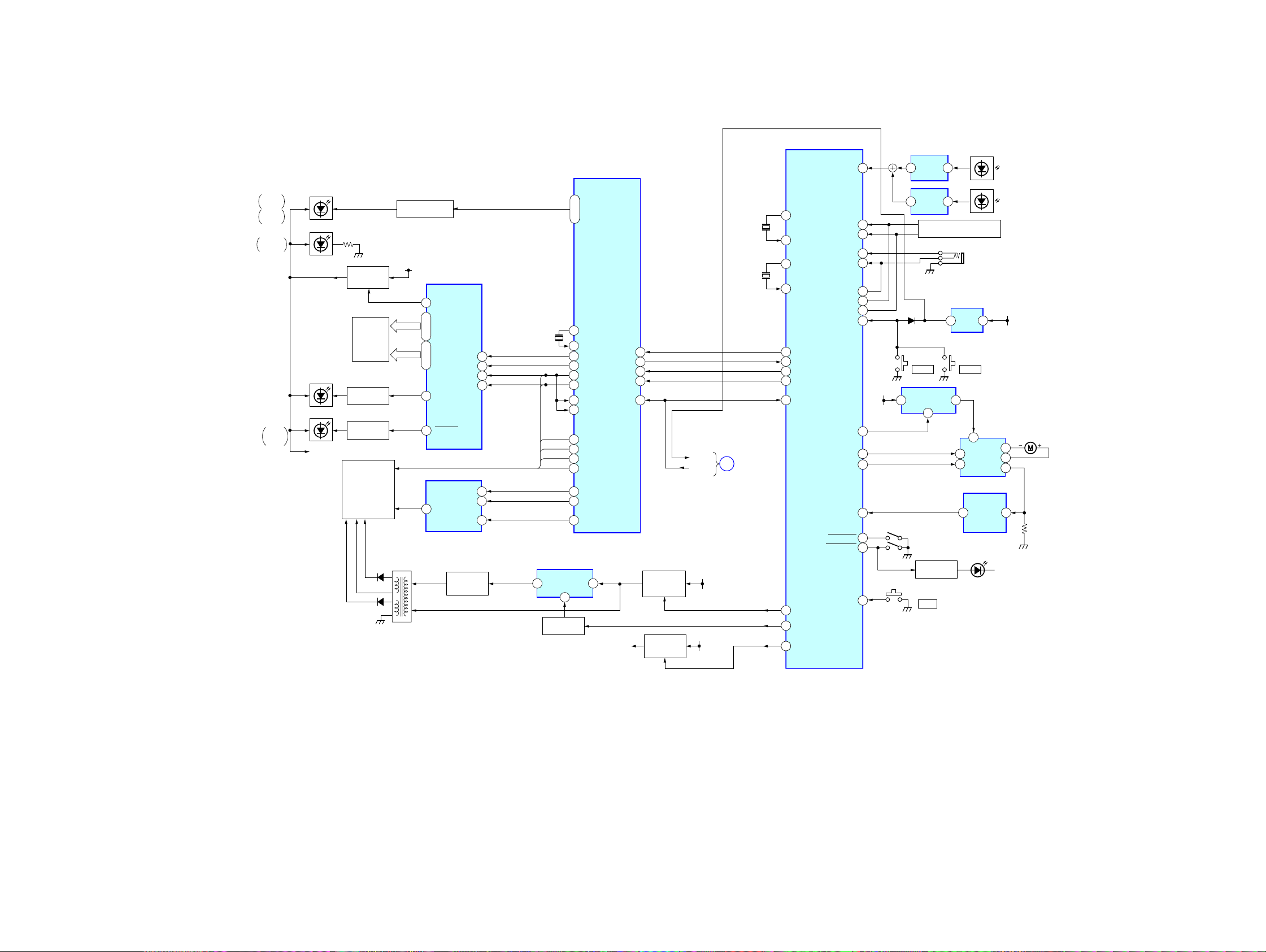
3-2. BLOCK DIAGRAM — MAIN SECTION —
PJ501
(ANTENNA)
AU +8V
+5V REG.
Q501
TUNER UNIT
1
VCC
10
TU_VDD
11
MUTE-CONDITION
TUX501
S_METER
TU_SDA
TU_SCL
TU MUTE
E2P_SDA
E2P_SCL
ELECTRONIC VOLUME
IC401
CD
SECTION
(Page 15)
BUS AUDIO IN
AUX IN
L
4
R
3
SDA
14
SCL
13
7
8
6
17
16
SCL
SDA
SA CLK
23
28
27
32
73
82
33
34
SYSTEM CONTROL
SA_CLK
I2C_SIO
I2C_SCO
TUNER ATT
TU ATT IN
VSM
EESIO
EECKO
A
JP401 (1/2)
L
R
IC303 (2/3)
CD-L
R-CH
Q408
BUS/AUX
SA_IN
VOLATT
BEEP
AMP_STB
AMP_DIAG
66
83
26
20
41
40
SA CLK
SDA
SCL
42
43
40
41
14
12
13
16
15
4
7
MDL
MDR
PDL+
PDR+
AML
AMR
SA IN
SDA
SCL
SAOUT
MUTE
OUT SW
CREF
OUT LF
OUT RF
OUT LR
OUT RR
17
38
25
22
24
21
IC470 (2/2)
BUFFER
5 7
R-CH
AMP
BIAS
LINE AMP
IC431
5
3 1
LINE AMP
IC451
SUB OUT AMP
3
8
2 24
11 13
5 23
7
MUTE DRIVER
Q401,402
IC470 (1/2)
LINE AMP
IC402
MUTE
Q450
MUTE
Q453
1
14
POWER AMP/POWER SUPPLY
IC201
12
11
SDA
SCL
16
22
25
2
4
SDA
SCL
ACGND
STB
DIAG
SW1
SW2
MUTE
Q470
MUTE
Q271,171
MUTE
Q281,181
5
3
9
7
R-CH
29
27
CN401
PJ401 (2/2)
CNP101
1
9
2
10
4
12
3
11
5
6
SUB OUT (MONO)
L
FRONT
R
L
REAR
R
FL+
FL–
RL+
RL-
FR+
FR–
RR+
RR–
AMP-R
ANT-R
AUDIO OUT
CNP102
BUS
CONTROL
IN
CD
SECTION
3
2
1
B
(Page 15)
DISPLAY
SECTION
C
(Page 17)
CDX-M8810/M8815X
8
6
5
4
7
LINK_ON/OFF
SYS_RST
UNI_SO
UNI_SI
UNI_CLK
BUS_ON
BU_CHK
A_ATT
CNVSS
RESET
B ATT
TH100
D105
D104
BATTERY CHECK
Q101
BUS ON SWITCH
Q110,111
LINK ON/OFF
SWITCH
Q112
D302
BUS INTERFACE
3
BATT
6
DATA I/O
4
CLK
1
BUSON
2
RST
D125
IC110
DATA OUT
DATA IN
CLK-IN
BUSON
B-CHK
RST
10
8
9
11
12
13
D301
D126
D906 D904
18
BU_IN
30
UNI_SI
29
UNI_SO
31
UNI_CKO
64
BUS_ON
65
SYSRST
25
ATT
TEL ATT
ILL _IN
ACC_IN
TEST IN
AU 8V
U-COM5V
A_3.3V
D_3.3V
DR_6V
LCD_10V
BATT
24
69
68
63
BU_3.3V U-COM 5V
30
REG1
37
REG2
31
REG3
VP2
33
34
ILLUM CHECK
ACC CHECK
VP1
REG4
REG5
ATT
Q103
Q907
Q102
+3.3V REG.
3 2
IC271
6
20
35
VP
19
17
F901
18
16
+B
13
ATT
14
ILL
7
ACC
15
TEST
• R-ch is omitted due to same as L-ch.
• Signal path
: FM
: AM/MW
: CD
1616
3-3. BLOCK DIAGRAM — DISPLAY SECTION —
MENU
ILLUM
RING
ILLUM
BUTTON
ILLUM
LED931
(OPEN)
LED943
(IMAGE)
LED955
LCD
BACK
LIGHT
LCD_10V
LED B+
SWITCH
Q903,904
LCD2
LIQUID
CRYSTAL
DISPLAY
LED DRIVER
Q908
LED DRIVER
Q905
FL 900
FLUORESCENT
INDICATOR
TUBE
F1(-)
F2(+)
FL_VDD
D623,624
D622
LED DRIVER
Q906,Q909-915
LCD_10V
GCP
T620
84
1
I
SEG59
59
83
COM1
I
COM8
76
85
86
11
LCD DRIVER
IC10
LED_SW2
SEG1
I
I
LCD_INH
LCD_CE1
LCD_CLK
LCD_DATA
LED_SW1
DIMMER
BUFFER
IC301
ON/OFF
DRIVE
Q620
97
98
99
100
2
1
5
X301
6.75MHz
DC-DC
CONVERTER
IC620
OUT
CT
7
SWITCH
Q621,622
100
75
I
68
11
13
37
36
35
33
5
24
22
99
3
23
25
21
FL DRIVER
LED_SW3
I
LED_SW10
XOUT
XIN
LCD_INH
LCD_CE
FL_CLK
FL_DAT1
FL_CLK_IN
FL_CLK_IN
LAT
BK
FL_DAT2
FL_DAT3
GCP2
GCP1
GCP3
54
V+
IC2
SYS_CLK
SYS_CE
SYS_SO
SYS_SI
CNVSS
1
29
30
31
7
POWER
CONTROL
Q623,642
POWER
CONTROL
Q914,916
RESET
CNVSS
BU3.3VFL3.3V
BATT
X301
32.768MHz
MAIN
C
SECTION
(Page 16)
X302
6MHz
SYSTEM CONTROL
IC303 (3/3)
9
XOUT
8
XIN
11
OSC OUT
13
OSC IN
95
DISP_CE
98
DISP SI/RX
99
DISP SO/TX
100
DISP CKO
7
CNVSS
93
FL_ON
22
FSW_OUT
92
FLD_ON
SIRCS
KEYIN0
KEYIN1
RC IN1
RC IN0
KEY_ACK2
KEY_ACK0
KEY_ACK1
RESET
MOTOR ON
MOT+
MOT-
FP-I_DET
OPEN_SW
CLOSE_SW
OPEN_KEY
CDX-M8810/M8815X
IR
RECEIVE
1
85
84
70
86
87
88
89
10
BATT
53
58
57
81
55
54
90
7
7
D907
1
IC62
IR
RECEIVE
IC503
KEY IN
MATRIX
S932
RESET
+9V REG
IC703
2
S601 (OPEN)
S602 (CLOSE)
LED DRIVER
Q503,504
S931
OPEN
1
1
S911-921
S901-910
(REMOTE IN)
IC302
RESET
1 2
SW501
RESET
3
3
4
7 5
(DISC IN)
CNJ101
1
MOTOR
DRIVE
IC702
MOTOR
CURRENT
DETECT
IC701
D512
D70
(IR RECEIVER)
D513
(IR RECEIVER)
BU3.3V
M904
(OPEN/CLOSE)
9
7
6
CDX-M8810/M8815X
17 17
CDX-M8810/M8815X
)
SENSOR board
SERVO board
• NOTE FOR PRINTED WIRING BOARDS AND SCHEMATIC DIAGRAMS3-4. CIRCUIT BOARDS LOCATION
THIS NOTE IS COMMON FOR PRINTED WIRING
BOARDS AND SCHEMATIC DIAGRAMS.
(In addition to this, the necessary note is printed
in each block.)
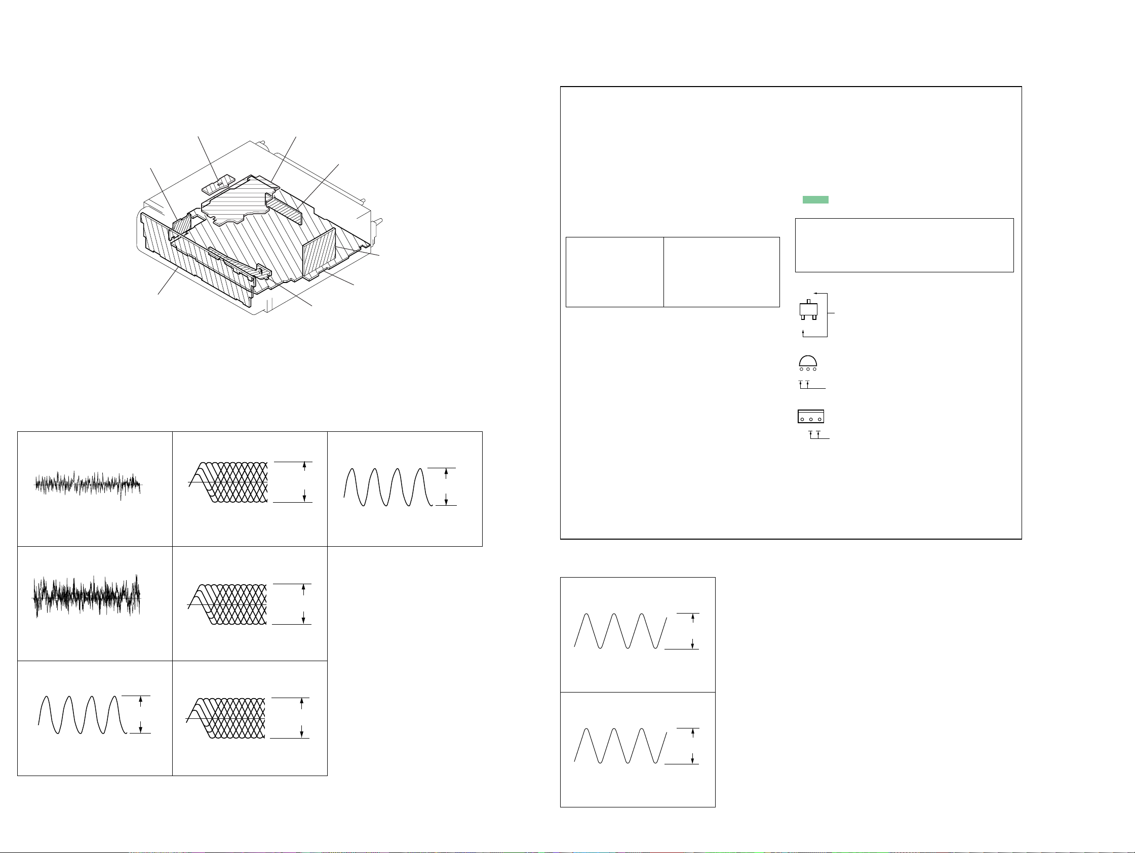
• WA VEFORMS
— SERVO BOARD —
(CD PLAY)
1
IC2 4 (FEI)
Approx. 100 mVp-p
50 mV/DIV, 5 msec/DIV
SWITCH board
DISPLAY board
0 V
4
IC2 uj (RFI)
0.5 V/DIV, 0.5 µsec/DIV
Approx.
1Vp-p
SPEAKER board
MAIN board
SUB board
7
IC3 ia (X1)
0.5 V/DIV, 0.2 µsec/DIV
tuner unit
(TUX501
12 MHz
1.1 Vp-p
For schematic diagrams.
Note:
• All capacitors are in µF unless otherwise noted. (p: pF)
50 WV or less are not indicated except for electrolytics
and tantalums.
• All resistors are in Ω and 1/
specified.
f
•
• C : panel designation.
Note:
The components identified by mark 0 or dotted
line with mark 0 are critical for safety.
Replace only with part
number specified.
• A : B+ Line.
• B : B– Line.
• H : adjustment for repair.
•Voltages and wavefor ms are dc with respect to ground
• CD mechanism section (1/2), (2/2)
no mark : CD PLAY
• Main (1/4), (2/4), (3/4), (4/4) and Display sections
no mark : FM
: internal component.
under no-signal (detuned) conditions.
(): AM/MW/LW
<>: CD PLAY
4
W or less unless otherwise
Note:
Les composants identifiés par
une marque 0 sont critiques
pour la sécurité.
Ne les remplacer que par une
piéce portant le numéro
spécifié.
∗ : Impossible to measure
•Voltages are taken with a V OM (Input impedance 10 MΩ).
Voltage variations may be noted due to nor mal production tolerances.
•Waveforms are taken with a oscilloscope.
Voltage variations may be noted due to nor mal production tolerances.
• Circled numbers refer to waveforms.
• Signal path.
J : CD PLAY
F : FM
f : AM
For printed wiring boards.
Note:
• X : parts extracted from the component side.
• Y : parts extracted from the conductor side.
a
•
• : Pattern from the side which enables seeing.
(The other layers' patterns are not indicated.)
Caution:
Pattern face side: Parts on the pattern face side seen from the
(Side B) pattern face are indicated.
Parts face side: Parts on the parts face side seen from the
(Side A) parts face are indicated.
: Through hole.
C
Q
These are omitted
EB
E
CB
These are omitted
C
BE
These are omitted
2
IC2 6 (TEI)
Approx. 400 mVp-p
200 mV/DIV, 5 msec/DIV
3
IC2 wd (XI)
16.9344 MHz
0.2 V/DIV, 0.2 µsec/DIV
CDX-M8810/M8815X
0 V
0.6 Vp-p
5
IC2 of (FNI2),
0.5 V/DIV, 0.5 µsec/DIV
6
IC2 oh (FPI2),
0.5 V/DIV, 0.5 µsec/DIV
og (FNI1)
1.5 Vp-p
oj (FPI1)
1.5 Vp-p
— MAIN BOARD —
1
IC303 9 (XOUT)
0.7 Vp-p
32.768 kHz
0.2 V/DIV, 20 µsec/DIV
2
IC303 qa (OSCOUT)
1.1 Vp-p
6 MHz
0.5 V/DIV, 0.2 µsec/DIV
1818
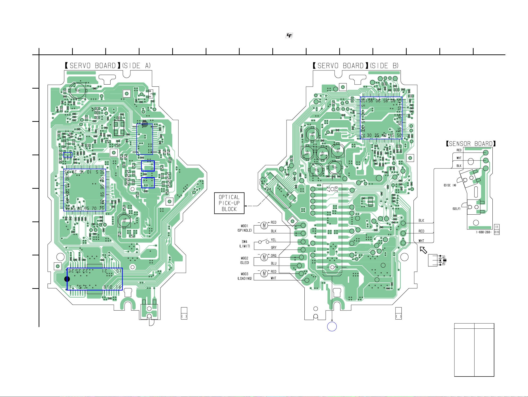
3-5. PRINTED WIRING BOARDS — CD MECHANISM SECTION — • Refer to page 18 for Circuit Boards Location. : Uses unleaded solder.
CDX-M8810/M8815X
A
B
C
D
E
F
G
1
FMA3
C22
R21
C102
C72
C80
C29
R84
C32
C65
C20
R86
R73
R13
R37
IC6
R39
R10
C35
TP39
Q3
Q2
C106
C64
234567891011 12 13 14
TP27
TP26
TP29
R29
R8
C9
C19
R71
R122
R70
C67
R68
TP40
C51
C62
R69
R11
C57
R66
IC3
R65
TP53
R9
R56
R57
C39
C41
R58
R16
R101
R132
C48
R48
R54
R42
R47
TP51
IC1
C38
C40
R40
R25
R50
R100
R17
C45
R123
R12
TP30
R41
FB4
C43
TP48
TP37
TP38
R89
C101
TP49
R43
C6
R26
FMA4
C103
C37
C73
R130
R103
R106
R107
R120
FB2
IC4
FB5
FMA6
R99
C90
R30
FB3
C61
C81
R129
R98
R108
C74
FB8
R7
R110
R94
C92
C93
TP14
R6
TP18
C66
C85
C96
(DOWN)
C7
C86
SW1
IC7
IC5
IC8
FMB3
TP22
Q1
TP17
R93
R92
C10
R4
TP13
TP16
C4
R1
TP88
C5
TP92
FMB5
TP2
TP1
TP9
TP8
TP11
C77
C82
R88
C91
C94
R95
C75
R97
FMA5
R96
C89
R102
R105
R104
R109
R111
TP12
CN1
TP24
R5
TP20
TP89
TP90
TP91
TP10
TP6
TP7
TP97
TP99
C76
C83
TP21
C95
TP15
C78
R114
TP68
C84
TP36
C70
R124
C100
CN2
C33
C99
C79
R115
TP42
TP35
TP95
TP34
TP41
C104
TP33
C42
TP43
TP74
TP77
TP79
TP81
TP83
TP85
TP93
C27
C34
R128
R64
TP44
R28
X1
TP78
TP82
TP80
TP31
TP23
C16
C49
R125
R63
TP101
TP76
R53
R127
R117
R67
R55
TP98
TP84
TP86
IC2
R62
TP87
C17
C23
R126
R60
TP66
R91
TP75
TP32
R2
C13
R61
R82
R59
R78
R118
R83
R81
C18
R121
TP62
R116
R74
C21
R72
TP65
C52
R3
TP25
C24
C53
R119
R77
C31
R22
TP47
R52
R90
C105
R23
R24
TP3
TP4
TP5
R19
C36
TP46
C47
TP64
TP67
C28
TP63
R44
FMB4
R80
SW3
SW2
X1
H
CDX-M8810/M8815X
1-864-900-
11
11
1-864-900-
A
MAIN BOARD CNP301
(Page 23)
11
11
• Semiconductor
Location
Ref. No. Location
IC1 G-2
IC2 B-11
IC3 D-2
IC5 C-4
IC6 D-1
IC7 D-4
IC8 D-4
Q1 B-4
Q2 C-1
Q3 C-1
19 19
 Loading...