

Page 1
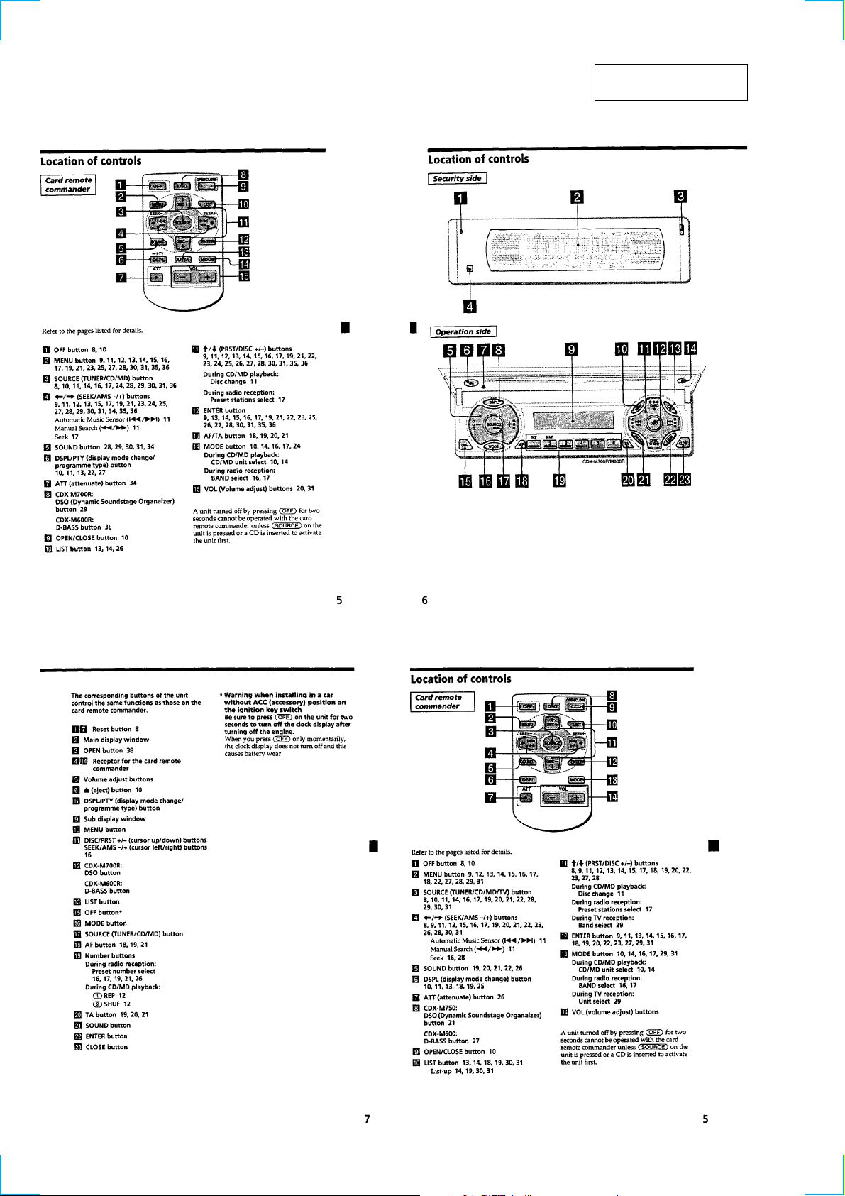
CDX-M700R/M750
SERVICE MANUAL
Ver 1.1 2000. 08
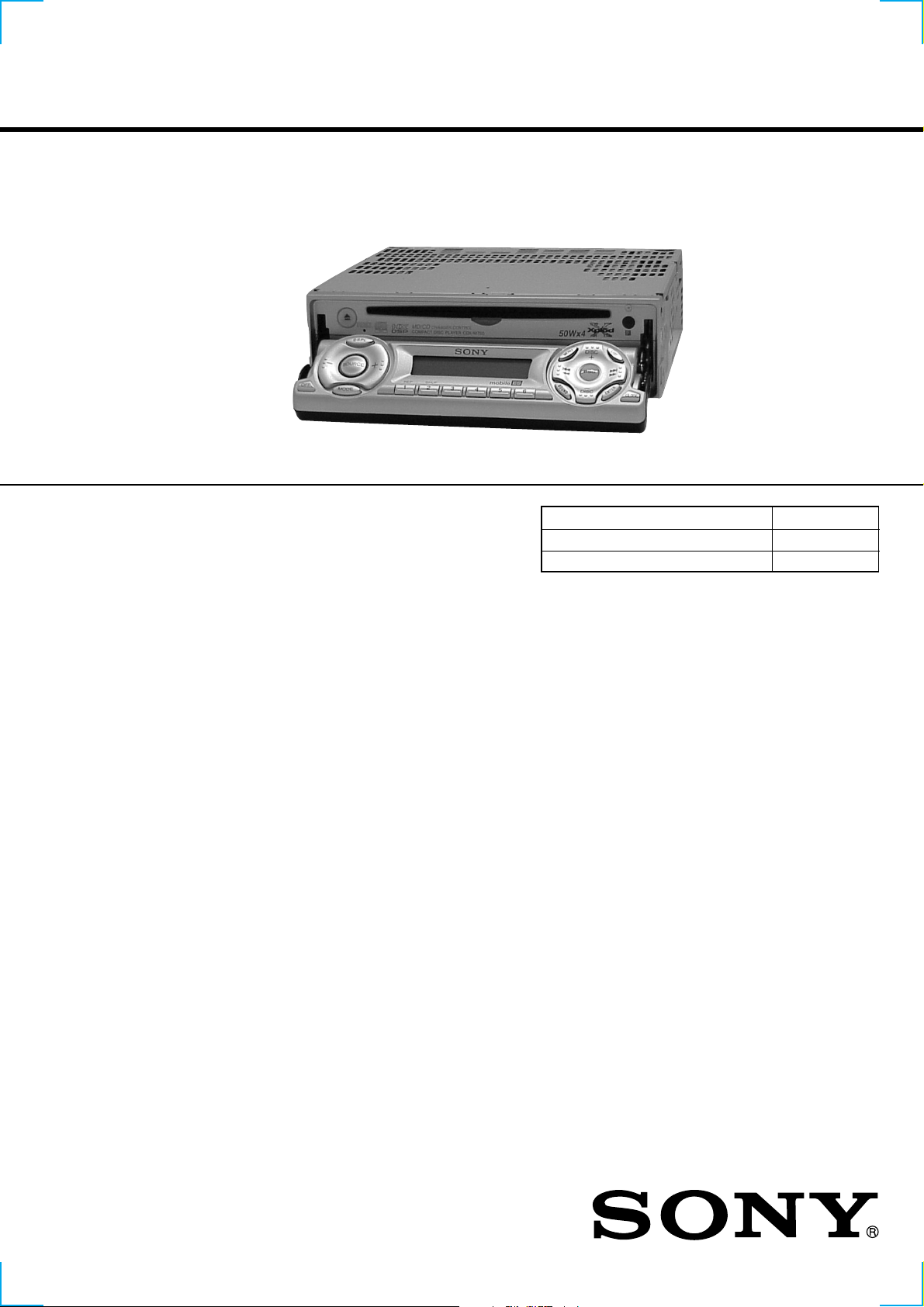
Photo: CDX-M750
• The tuner and CD sections have no adjustments.
SPECIFICATIONS
AUDIO POWER SPECIFICATIONS (CDX-M750)
POWER OUTPUT AND TOTAL HARMONIC DISTORTION
19 watts per channel minimum continuous average power into
4 ohms, 4 channels driven from 20 Hz to 20 kHz with no more
than 1% total harmonic distortion.
Other Specifications
CD player section
System Compact disc digital audio
Signal-to-noise ratio 90 dB
Frequency response 10 – 20,000 Hz
Wow and flutter Below measurable limit
Laser Diode Properties (CDX-M750)
Material GaAlAs
Wavelength 780 nm
Emission Duration Continuous
Laser output power Less than 44.6 µW*
* This output is the value measured at a distance
of 200 mm from the objective lens surface on the
Optical Pick-up Block.
Tuner section
FM
Tuning range 87.5 – 107.9 MHz (CDX-M750)
Antenna terminal External antenna connector
Intermediate frequency 10.7 MHz/450 kHz
Usable sensitivity 8 dBf
Selectivity 75 dB at 400 kHz
Signal-to-noise ratio 66 dB (stereo),
Harmonic distortion at 1 kHz
Separation 35 dB at 1 kHz
Frequency response 30 – 15,000 Hz
AM (CDX-M750)
Tuning range 530 – 1,710 kHz
Antenna terminal External antenna connector
Intermediate frequency 10.7 MHz/450 kHz
Sensitivity 30 µV
system
87.5 – 108.0 MHz (CDX-M700R)
72 dB (mono)
0.6% (stereo),
0.3% (mono)
FM/MW/LW COMPACT DISC PLAYER
US Model
CDX-M750
AEP Model
UK Model
CDX-M700R
Model Name Using Similar Mechanism NEW
CD Drive Mechanism Type MG-383V-121//K
Optical Pick-up Name KSS-720A
MW/LW (CDX-M700R)
Tuning range MW: 531 – 1,602 kHz
LW: 153 – 279 kHz
Aerial terminal External aerial connector
Intermediate frequency 10.7 MHz/450 kHz
Sensitivity MW: 30 µV
LW: 40 µV
Power amplifier section
Outputs Speaker outputs
Speaker impedance 4 – 8 ohms
Maximum power output 50 W × 4 (at 4 ohms)
General
Outputs Audio outputs (3)
Power antenna relay
control lead (CDX-M750)
Power aerial relay
control lead (CDX-M700R)
Power amplifier control
lead
Inputs Telephone ATT control
lead
Illumination control lead
Power requirements 12 V DC car battery
(negative ground)
– Continued on next page –
FM/AM COMPACT DISC PLAYER
CDX-M750
CDX-M700R
1
Page 2
Ver 1.1 2000. 08
k
Dimensions Approx. 178 × 50 × 182 mm
(7 1/8 × 2 × 7 1/4 in.)
(w/h/d)
Mounting dimensions Approx. 182 × 53 × 163 mm
(7 1/4 × 2 1/8 × 6 1/2 in.)
(w/h/d)
Mass Approx. 1.5 kg (3 lb. 1 oz.)
Supplied accessories Card remote commander
RM-X92 (CDX-M750)
RM-X95 (CDX-M700R)
Parts for installation and
connections (1 set)
Design and specifications are subject to change without
notice.
SERVICE NOTES
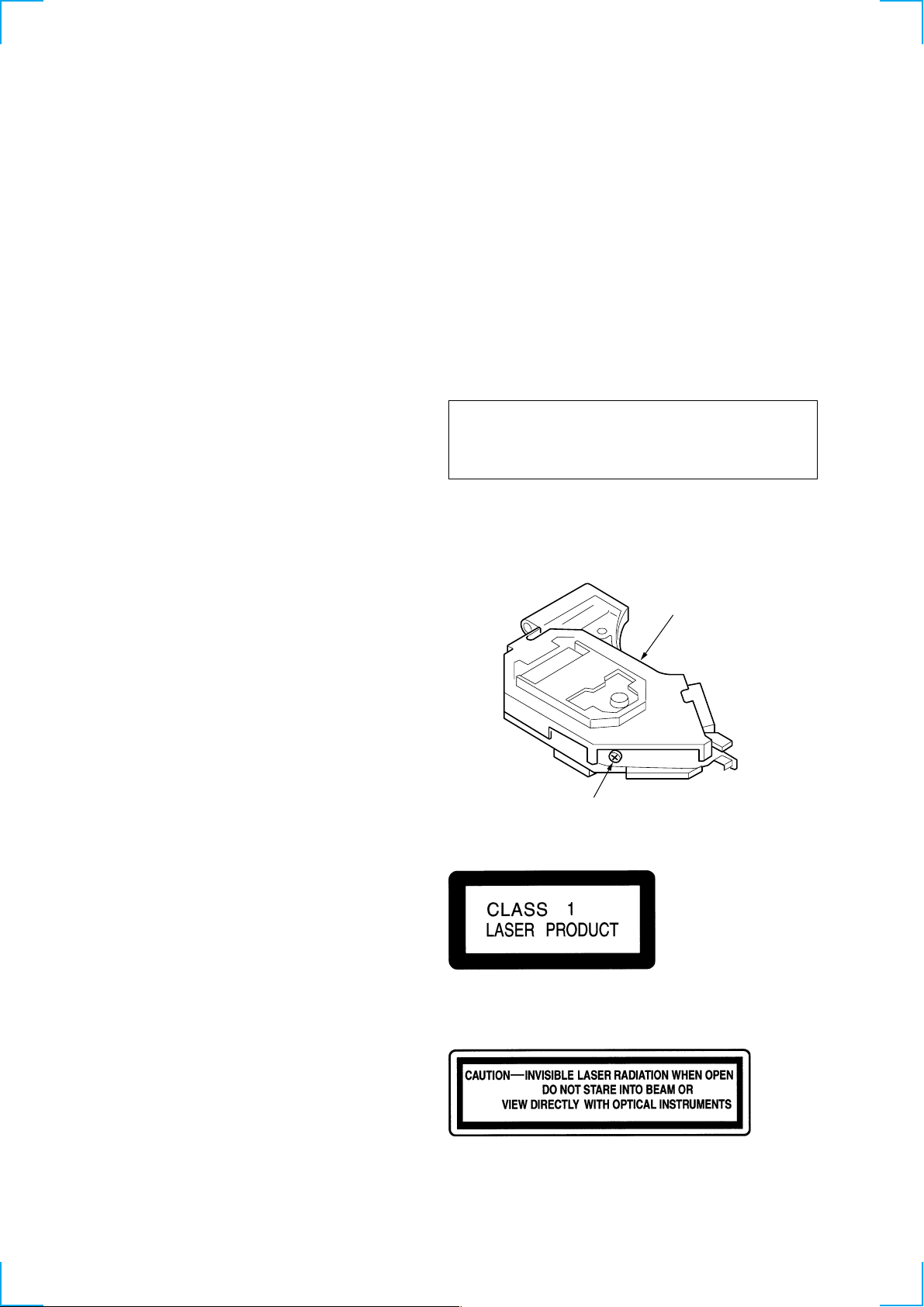
NOTES ON HANDLING THE OPTICAL PICK-UP BLOCK
OR BASE UNIT
The laser diode in the optical pick-up block may suffer electrostatic
breakdown because of the potential difference generated by the
charged electrostatic load, etc. on clothing and the human body.
During repair, pay attention to electrostatic breakdown and also use
the procedure in the printed matter which is included in the repair
parts.
The flexible board is easily damaged and should be handled with
care.
NOTES ON LASER DIODE EMISSION CHECK
The laser beam on this model is concentrated so as to be focused on
the disc reflective surface by the objective lens in the optical pickup block. Therefore, when checking the laser diode emission, observe from more than 30 cm away from the objective lens.
US model:
CAUTION
Use of controls or adjustments or performance of procedures
other than those specified herein may result in hazardous
radiation exposure.
If the optical pick-up block is defective, please replace the whole
optical pick-up block.
Never turn the semi-fixed resistor located at the side of optical
pick-up block.
optical pick-up bloc
Notes on Chip Component Replacement
• Never reuse a disconnected chip component.
• Notice that the minus side of a tantalum capacitor may be dam-
aged by heat.
SAFETY-RELATED COMPONENT WARNING!!
COMPONENTS IDENTIFIED BY MARK 0 OR DOTTED LINE
WITH MARK 0 ON THE SCHEMATIC DIAGRAMS AND IN
THE PARTS LIST ARE CRITICAL TO SAFE OPERATION.
REPLACE THESE COMPONENTS WITH SONY PARTS WHOSE
P ART NUMBERS APPEAR AS SHOWN IN THIS MANU AL OR
IN SUPPLEMENTS PUBLISHED BY SONY.
semi-fixed resistor
AEP/UK model:
This product is classified as a CLASS 1 LASER PRODUCT.
This label is located on the bottom of the
chassis.
This label is located on the drive unit's internal
chassis.
When replacing the chassis (T) of mechanism deck which have
the “CAUTION LABEL” attached, please be sure to put a new
CAUTION LABEL (3-223-913-11) to the chassis (T).
2
Page 3
Ver 1.1 2000. 08
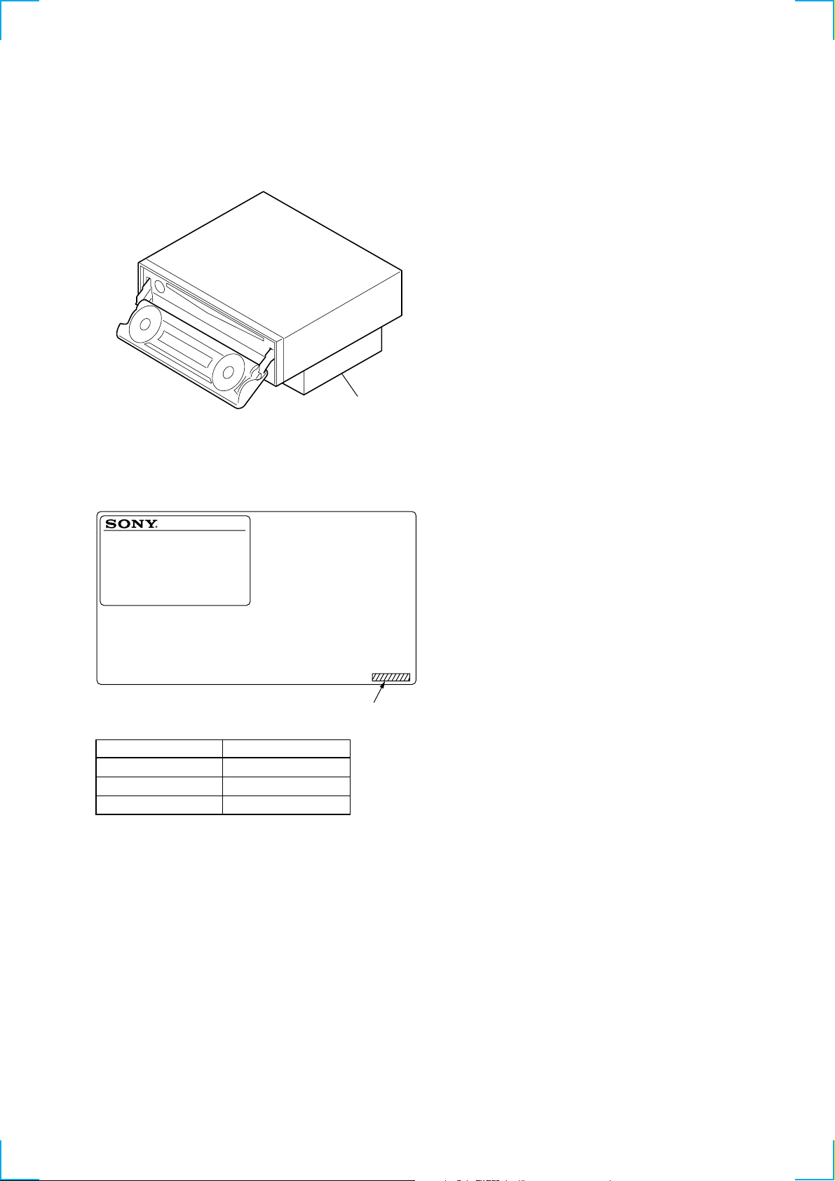
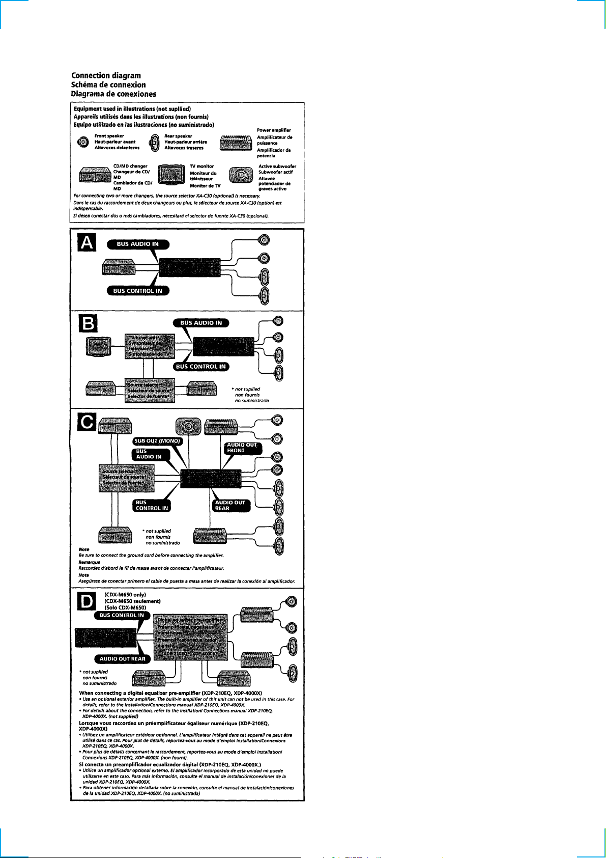
NOTE FOR THE OPENING OF THE FRONT PANEL
In this set, the front panel is lowered to below the bottom face when
it is opened.
When servicing the set, place it on a stand having a height of about
2 cm.
stand
MODEL IDENTIFICATION
CDX-M700R have 3 type models.
– MODEL NUMBER LABEL –
MODEL No. CDX-M700R
FM/MW/LW COMPACT DISC PLAYER
TABLE OF CONTENTS
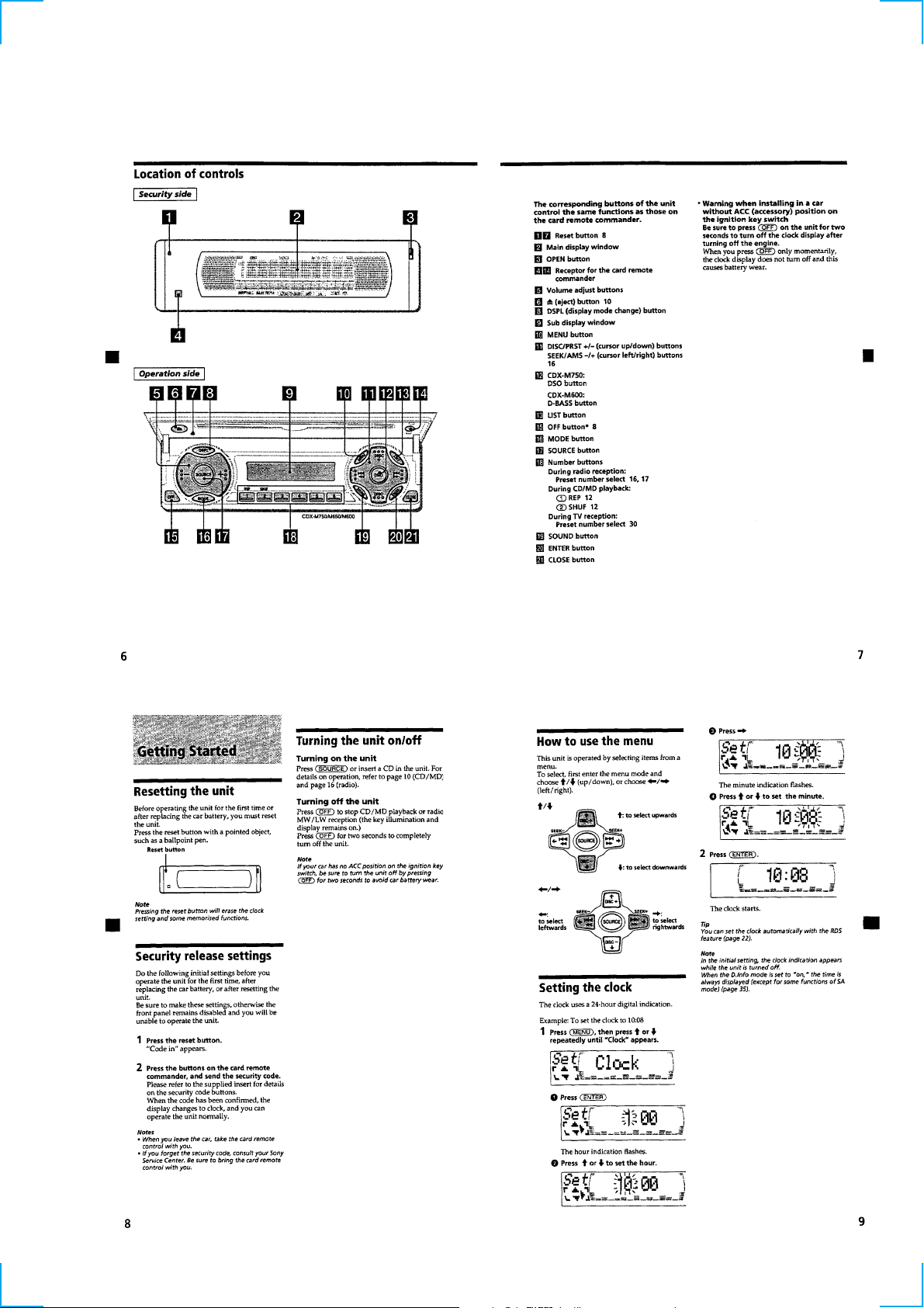
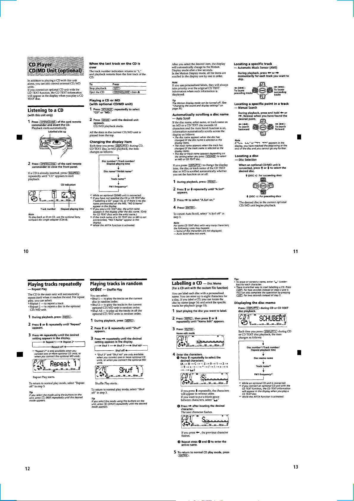
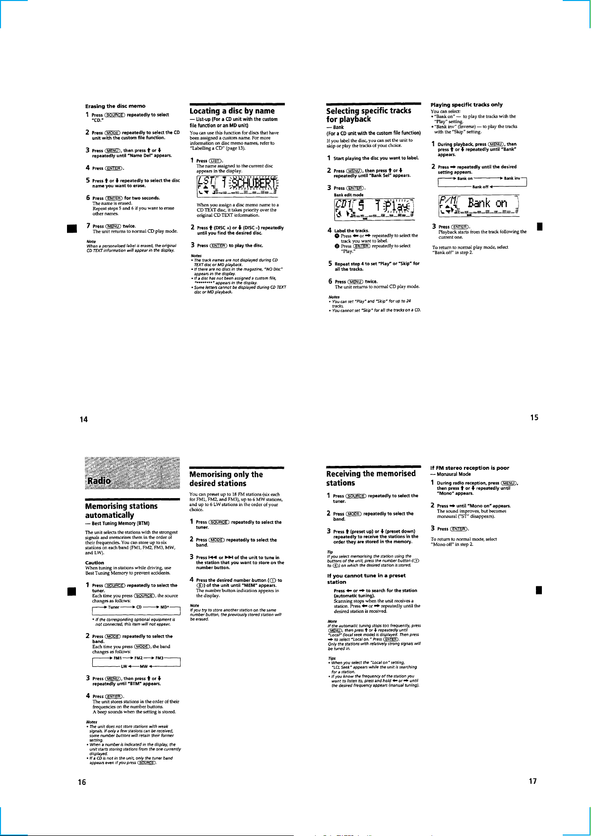
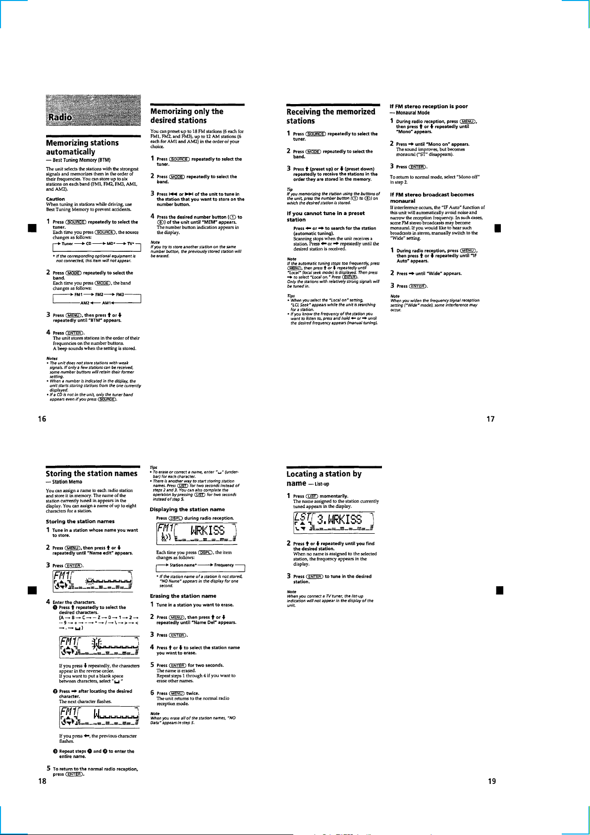
1. GENERAL
Location of controls................................................................. 4
Getting Started......................................................................... 5
Setting the clock ...................................................................... 5
CD Player CD/MD Unit .......................................................... 6
Radio ....................................................................................... 7
RDS ......................................................................................... 9
DAB....................................................................................... 10
DSP........................................................................................ 11
Other Functions ..................................................................... 12
TV/Video ...............................................................................14
Connections ........................................................................... 15
2. DISASSEMBLY
2-1. Front Panel Assy (Normal)................................................ 22
2-2. Front Panel Assy (Inoperative).......................................... 22
2-3. CD Mechanism Block, Flexible Board ............................. 23
2-4. Sub Panel (CD) Sub Assy ................................................. 23
2-5. Motor Block Assy, Cam (R) Assy ..................................... 24
2-6. Main Board ....................................................................... 24
2-7. Heat Sink ...........................................................................25
2-8. Chassis (T) Sub Assy ........................................................ 25
2-9. Lever Section..................................................................... 26
2-10. Servo Board....................................................................... 26
2-11. Shaft Roller Assy .............................................................. 27
2-12. Floating Block Assy .......................................................... 27
2-13. Optical Pick-up Block ....................................................... 28
Part No. Model
3-046-061-0s TYPE1
3-046-062-0s TYPE2
3-047-828-0s TYPE3
Part No.
3. PHASE ALIGNMENT
3-1. Arm (A-L) Assy, Arm (B-L) Assy..................................... 29
3-2. Cam (L) ............................................................................. 29
3-3. Motor Block ...................................................................... 30
3-4. Alignment between Arm (A-L) Assy
and Arm (B-L) Assy .......................................................... 30
3-5. Arm (A-R) Assy, Arm (B-R) Assy .................................... 31
3-6. Cam (R) ............................................................................. 31
4. DIAGRAMS
4-1. IC Pin Descriptions ........................................................... 32
4-2. Block Diagram –CD Section–........................................... 42
4-3. Block Diagram –Tuner Section–....................................... 43
4-4. Block Diagram –Display Section–.................................... 44
4-5. Circuit Boards Location .................................................... 45
4-6. Printed Wiring Boards –CD Mechanism Section–............ 46
4-7. Schematic Diagram –CD Mechanism Section (1/2)– ....... 48
4-8. Schematic Diagram –CD Mechanism Section (2/2)– ....... 49
4-9. Printed Wiring Boards –Main Section– ............................ 50
4-10. Schematic Diagram –Main Section (1/4)– ........................ 52
4-11. Schematic Diagram –Main Section (2/4)– ........................ 53
4-12. Schematic Diagram –Main Section (3/4)– ........................ 54
4-13. Schematic Diagram –Main Section (4/4)– ........................ 55
4-14. Printed Wiring Board –Sub Section– ................................ 56
4-15. Schematic Diagram –Sub Section– ................................... 57
4-16. Printed Wiring Board –Display Section– .......................... 58
4-17. Schematic Diagram –Display Section–............................. 59
5. EXPLODED VIEWS
5-1. Chassis Section ................................................................. 62
5-2. Front Panel Section ........................................................... 63
5-3. CD Mechanism Section (1) ............................................... 64
5-4. CD Mechanism Section (2) ............................................... 65
5-5. CD Mechanism Section (3) ............................................... 66
6. ELECTRICAL PARTS LIST ........................................ 67
3
Page 4
CDX-M700R
SECTION 1
GENERAL
This section is extracted
from instruction manual.
CDX-M750
4
Page 5
567
Page 6
Page 7
CDX-M700R
Page 8
CDX-M7509CDX-M700R
8
Page 9
Page 10
CDX-M700R
10
Page 11
111213
Page 12
Page 13
Page 14
CDX-M75015CDX-M700R
14
Page 15
Page 16
161718
Page 17
Page 18
Page 19
CDX-M750
19
Page 20
202122
Page 21
Page 22
SECTION 2
DISASSEMBLY
Note : Follow the disassembly procedure in the numerical order given.
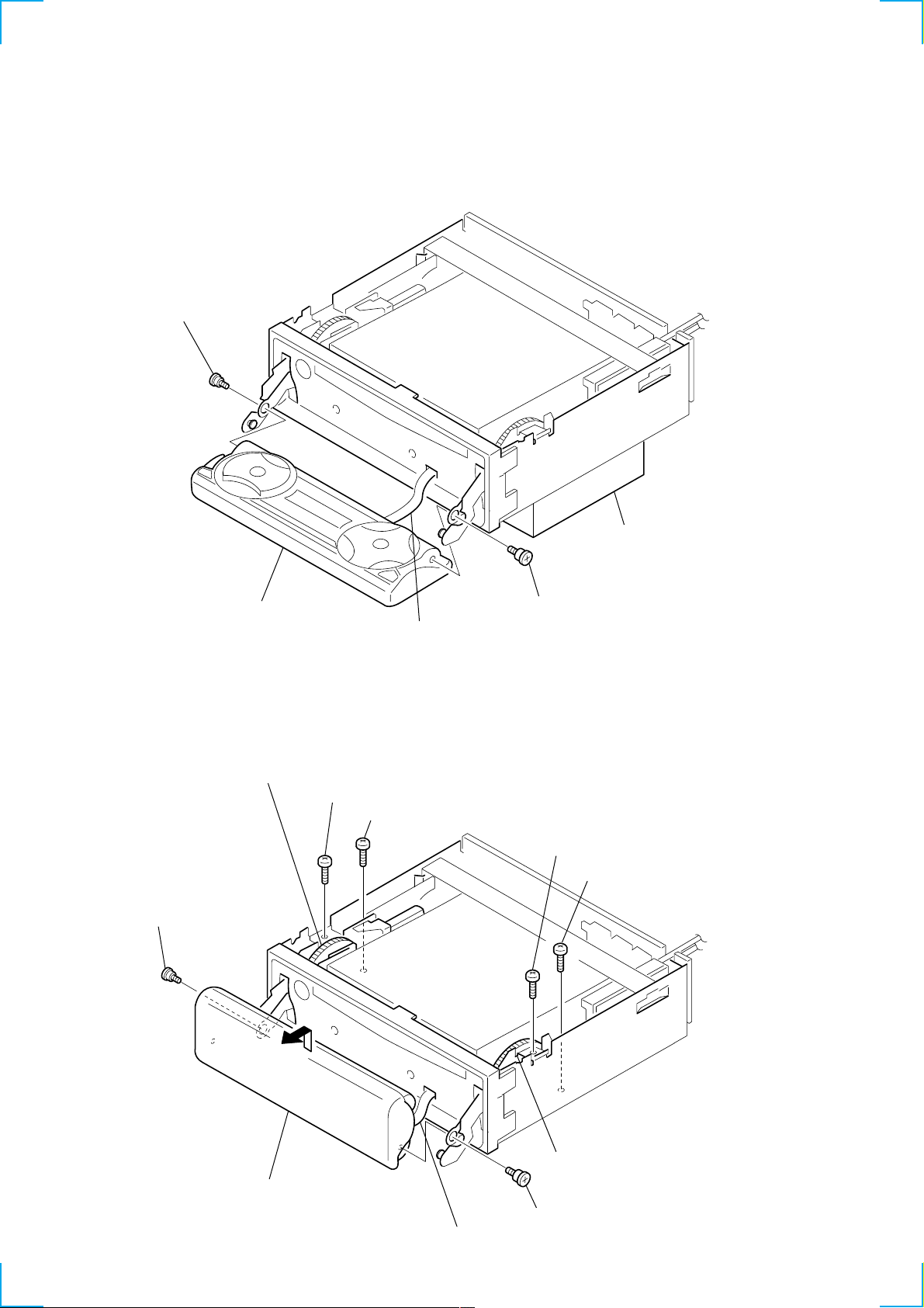
2-1. FRONT PANEL ASSY (NORMAL)
1 Turn on the power and open the front panel.
3 screw (panel)
4 front panel assy
(Take care not to
pull the flexible
board excessively.)
2-2. FRONT PANEL ASSY (INOPERATIVE)
8 Lift the motor block assy
slightly to make a play.
5 PTT 2.6x6
2 screw (panel)
stand
2 screw (panel)
flexible board
6 PTT 2.6x6
3 PTT 2.6x6
4 PTT 2.6x6
9
0 front panel assy
(Take care not to pull the
flexible board excessively.)
7 Lift the cam (R) assy
slightly to make a play.
1 screw (panel)
flexible board
Page 23
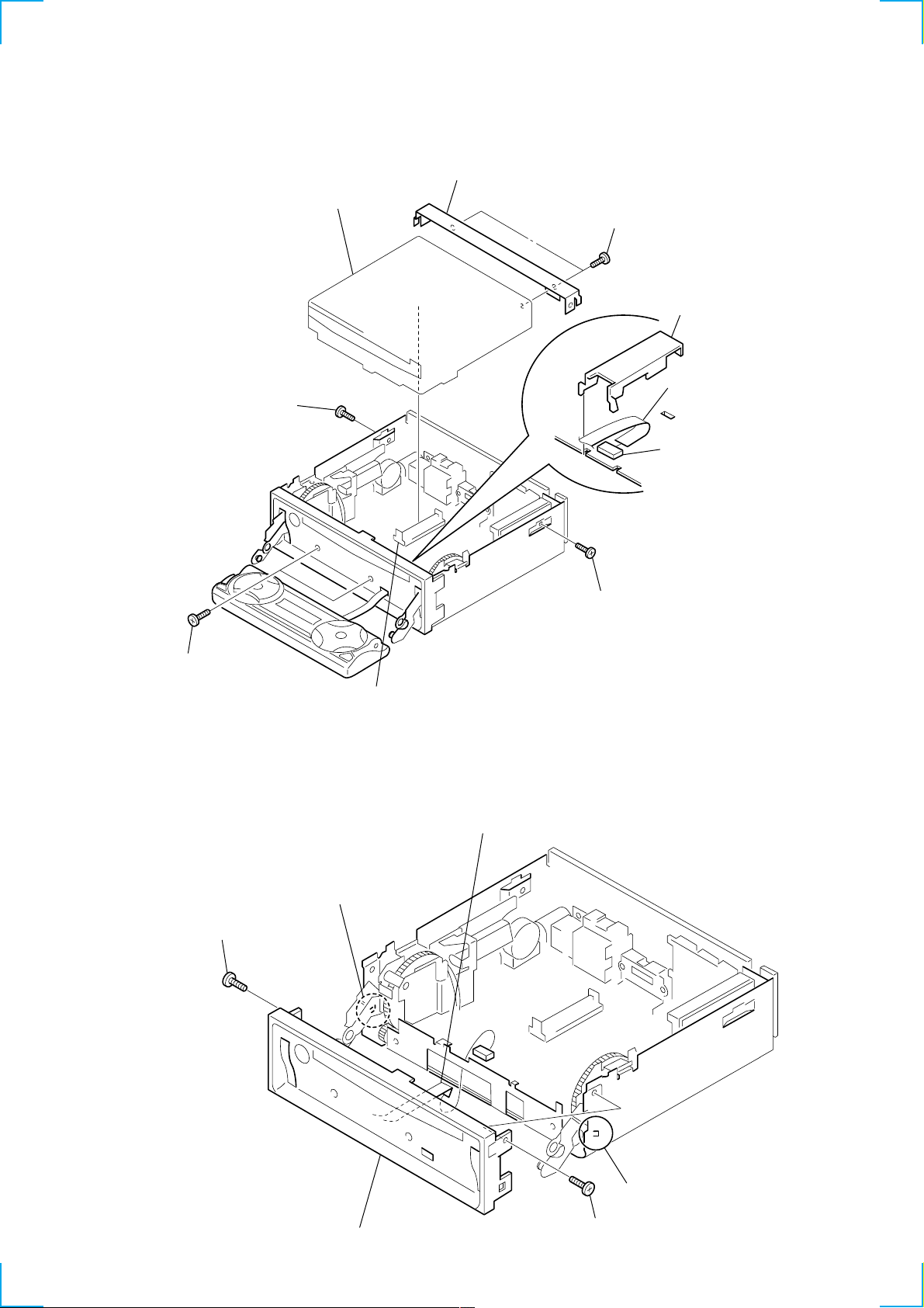
2-3. CD MECHANISM BLOCK, FLEXIBLE BOARD
5 CD mechanism block
3 PTT 2.6x4
7 bracket (CD)
6 PTT 2.6x6
8 cover (flexible)
0 flexible board
9 CNP802
Note: When installing
the flexible board,
make the board slack
as illustrated.
1 PTT 2.6x6
2-4. SUB PANEL (CD) SUB ASSY
4 claw
3 PTT 2.6x6
2 PTT 2.6x4
4 CNP701
1 CNP805
6 sub panel (CD) sub assy
5 claw
2 PTT 2.6 x6
23
Page 24
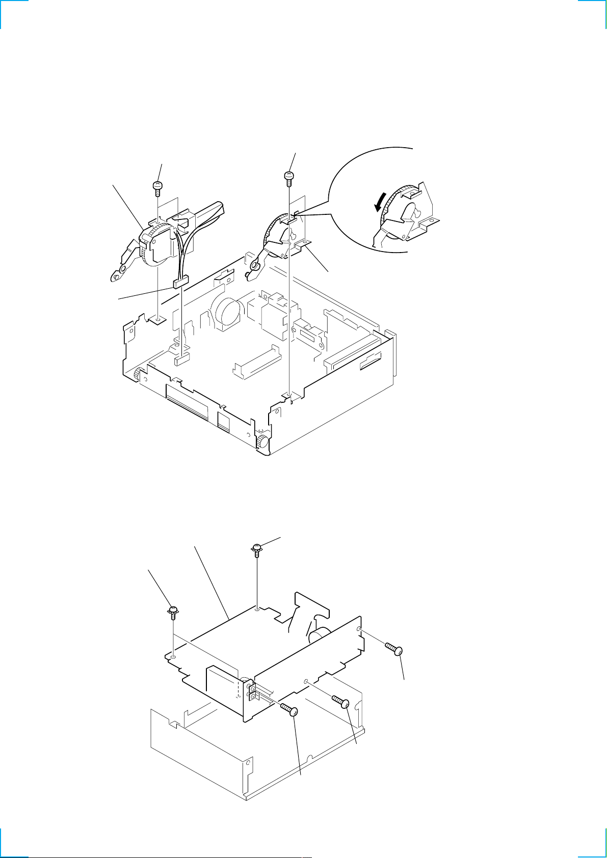
2-5. MOTOR BLOCK ASSY, CAM (R) ASSY
8
Note : Install the motor block assy and cam (R) assy in this roder.
For phase alignment between cams (L) and (R), see page 29 and 31.
5 motor block assy
3 CNP902
4 PTT 2.6x6
1 PTT 2.6x6
2 cam (R) assy
Note: Install the cam (R) assy with
the cam fully rotated in the
direction of the arrow A.
A
2-6. MAIN BOARD
6 MAIN board
5 PTT 2.6x6
ground point
4 PTT 2.6x6
ground point
1 PTT 2.6x8
3 PTT 2.6x
2 PTT 2.6x8
24
Page 25

2-7. HEAT SINK
8
5 heat sink
4 PTT 2.6x
3 PTT 2.6x8
2 PTT 2.6x12
1 PTT 2.6x8
2-8. CHASSIS (T) SUB ASSY
1 Unsolder the
lead wires.
2 P 2x3
3 P 2x3
4 chassis (T) sub assy
black
red
white
25
Page 26

2-9. LEVER SECTION
5 guide (disc)
6 lever (R)
3 tension spring (LR)
7 lever (L)
1 special screw
2 DISC IN SW board
2-10. SERVO BOARD
3 Removal the solders.
5 loading motor assy
4 claws
7 PS 2x4
6 PS 2x4
2 CN2
1 CN3
4 P 2x3
8 SERVO board
26
Page 27

Fig. 1
1 tension spring (RA)
2 arm (roller)
3 retaing ring (RA)
4 shaft retainer
5 shaft roller assy
retaing ring (RA)
arm
arm
washer
washer
shaft retainer
shaft retainer
2-11. SHAFT ROLLER ASSY
• When installing, take note of the positions
arm (roller) and washers. (Fig. 1)
2-12. FLOATING BLOCK ASSY
7 compression spring (FL)
5 Turn loading ring in the
direction of the arrow.
1 tension spring (KF1)
6 floating block assy
8 compression spring (FL)
4 Fit lever (D) in the
direction of the arrow.
3 damper (T)
2 damper (T)
27
Page 28

2-13. OPTICAL PICK-UP BLOCK
1 P 2x3
2 sled motor assy
3 optical pick-up block
28
Page 29

)
3-1. ARM (A-L) ASSY, ARM (B-L) ASSY
y
4 arm (A-L) assy
3 spring (arm L)
SECTION 3
PHASE ALIGNMENT
5 stop ring 1.5, type-E
2 stop ring 1.5, type-E
1 arm (B-L) ass
3-2. CAM (L)
1 Move the arm (B-L) assy in the direction of the
arrow A and the arm (A-L) assy in the direction of
the arrow B fully (full open state).
2 Align the hole on the cam (L) with part C and install
the cam.
4 Turn the cam (L) clockwise and counterclockwise to
verify that both the arms are operated.
bracket (L) assy
3 stop ring 1.5, type-E
hole
cam (L
C
arm (B-L) assy
A
arm (A-L) assy
B
29
Page 30

3-3. MOTOR BLOCK
)
V
1 Turn the cam (L) and position the cam so that part A
does not touch the SWITCH board SW900.
SWITCH board
5 B 2.6x4
SW900
4 PTT 2.6x6
3 PTT 2.6x6
2 motor block
cam (L
3-4. ALIGNMENT BETWEEN ARM (A-L) ASSY
AND ARM (B-L) ASSY
1 Input 9V DC to the motor terminal until the cam (L)
stops rotating.
Take care to avoid overload of the motor.
2 Verify that the arm (A-L) assy and arm (B-L) assy
are positioned as shown below (full open).
arm (B-L) assy
A
motor
GND
DC 9
+B
30
arm (A-L) assy
Page 31

3-5. ARM (A-R) ASSY, ARM (B-R) ASSY
y
2 stop ring 1.5, type-E
5 stop ring 1.5, type-E
4 arm (A-R) ass
1 arm (B-R) assy
3-6. CAM (R)
1 Move the arm (B-R) assy in the direction of the
arrow A and the arm (A-R) assy in the direction of
the arrow B fully (full open state).
2 Align the hole on the cam (R) with part C and install
the cam.
4 Turn the cam (R) clockwise and counterclockwise to
verify that both the arms are operated.
3 spring (arm R)
bracket (R) assy
3 stop ring 1.5, type-E
hole
C
cam (R)
A
arm (B-R) assy
B
arm (A-R) assy
31
Page 32

SECTION 4
DIAGRAMS
4-1. IC PIN DESCRIPTIONS
• IC501 CXD2598Q (DIGITAL SERVO, DIGITAL SIGNAL PROCESSOR) (SERVO BOARD)
Pin No. Pin Name I/O Pin Description
1 DVDD — Digital power supply pin
2 DVSS — Digital ground
3 SOUT O Servo brock serial data output (Not used.)
4 SOCK O Servo brock serial data read clock output (Not used.)
5 XOLT O Servo brock serial data latch output (Not used.)
6 SQSO O Sub Q 80 bit, PCM peak and level data output. CD TEXT data output
7 SQCK I Clock input from SQSO read output.
8 SCSY I Fixed at “L”.
9 SBSO O Serial output of sub-P to W. (Not used.)
10 EXCK I Clock input from SBSO read output. (Fixed at “L”)
11 XRST I System reset (“L”: Reset)
12 STSM I System mute input (Fixed at “L”)
13 DATA I Serial data input from CPU.
14 XLAT I Latch input from CPU. Latch serial data at the falling edge.
15 CLOK I Serial data transfer clock input from CPU.
16 SENS O SENS output for CPU.
17 SCLK I Clock input from SENS serial data read.
18 ATSK I/O Input/output for anti-shock.
19 WFCK O WFCK (Write Flame Clock) output (Not used.)
20 XUGF O XUGF output (Not used.)
21 XPCK O XPCK output (Not used.)
22 GFS O GFS output
23 C2PO O C2PO output (Not used.)
24 SCOR O “H” output at either detection, sub code sync S0 or S1.
25 C4M O 4.2336 MHz output (Not used.)
26 WDCK O Word clock input f=2Fs (Not used.)
27 COUT I/O Track number count signal input/output (Not used.)
28 MIRR I/O Mirror signal input/output (Not used.)
29 DVSS — Digital ground
30 DVDD — Digital power supply pin
31 DFCT I/O Diffect signal input/output (Not used.)
32 FOK I/O Focus OK signal output
33 PWM1 I External control input of spindle motor.
34 LOCK I/O Lock signal input/output
35 MDP O Servo control output of spindle motor.
36 SSTP I Disc most inner track detection signal input
37 FSTIO I/O 2/3 frequency division output of pins ih and ij. (Not used.)
38 SFDR O Sled drive output
39 SRDR O Sled drive output
40 TFDR O Tracking drive output
41 TRDR O Tracking drive output
42 FFDR O Focus drive output
43 FRDR O Focus drive output
44 DVDD — Digital power supply pin
45 DVSS — Digital ground
46 TEST I Test pin (Fixed at “L”.)
47 TES1 I Test pin (Fixed at “L”.)
48 XTSL I X’tal select input (“L”: 16.9344 MHz, “H”: 33.8688 MHz)
49 VC I Center voltage input
50 FE I Focus error signal input
51 SE I Sled error signal input
32
Page 33

Pin No. Pin Name I/O Pin Description
52 TE I Tracking error signal input
53 CE I Center servo analog input
54 RFDC I RF signal input
55 ADIO O Test pin (Not used.)
56 AVSSO — Analog ground
57 IGEN I Constant current input from OP amplifier.
58 AVDDO — Analog ground
59 ASYO O EFM full-swing output (“L”: VSS, “H”: VDD)
60 ASYI I Asymmetry comparate voltage input
61 RFAC I EFM signal input
62 AVSS3 — Analog ground
63 CLTV I VCO control voltage input from master.
64 FILO O Filter output for master PLL. (slave=digital PLL)
65 FILI I Filter input from master PLL.
66 PCO O Charge pump output for master PLL.
67 AVDD3 — Analog power supply pin
68 BIAS I Asymmetry circuit constant current input
69 VCTL I VCO2 control input from wideband EFM PLL.
70 V16M O VCO2 oscillator output for wideband EFM PLL. (Not used.)
71 VPCO O Charge pump output for wideband EFM PLL. (Not used.)
72 DVSS — Digital ground
73 MD2 I Digital out ON/OFF control input (“L”: OFF, “H”: ON)
74 DOUT O Digital out output
75 ASYE I Asymmetry circuit ON/OFF input (“L”: OFF, “H”: ON)
76 DVDD — Digital power supply pin
77 LRCK O D/A interface LR clock output (f=Fs)
78 LRCKI I D/A interface LR clock input
79 PCMD O D/A interface serial data output (2’s COMP, MSB fast)
80 PCMD I D/A interface serial data input (2’s COMP, MSB fast)
81 BCK O D/A interface bit clock output
82 BCKI I D/A interface bit clock input
83 EMPH O Emphasis ON/OFF signal output
84 EMPHI I Emphasis ON/OFF signal input (“H”: ON, “L”: OFF)
85 XVDD — Power supply for master clock.
86 XTAI I X’tal oscillator input from master clock (16.9344 MHz).
87 XTAO O X’tal oscillator output for master clock (16.9344 MHz). (Not used.)
88 XVSS — Ground pin for master clock.
89 AVDD1 — Analog power supply pin
90 AOUT1 O Lch analog output (Not used.)
91 AIN1 I Lch OP amplifier input (Not used.)
92 LOUT1 O Lch LINE output (Not used.)
93 AVSS1 — Analog ground
94 AVSS2 — Analog ground
95 LOUT2 O Rch LINE output (Not used.)
96 AIN2 I Rch OP amplifier input (Not used.)
97 AOUT2 O Rch analog output (Not used.)
98 AVDD2 — Analog power supply pin
99 RMUT O Rch “0” detect Flug (Not used.)
100 LMUT O Lch “0” detect Flug (Not used.)
33
Page 34

• IC5 CXP84640-072Q (CD SYSTEM CONTROL) (SERVO BOARD)
Pin No. Pin Name I/O Pin Description
1 ITRPT — Not used in this set.
2, 3 ——Not used in this set.
4, 5 NCO — Not used in this set.
6 OPEN I Front panel open detection input
7 CLOSE O Front panel close control output
8 LINKOFF I Bus interface link input
9 NCO — Not used in this set.
10 D SW I Down switch input (SW1)
11 SSTP I Limit switch input (SW4)
12, 13 NCO — Not used in this set.
14, 15 ——Not used in this set.
16 EMPH O O De-emphasis ON/OFF control output
17 CDMON O CD mechanism deck power control output
18 CD ON O CD power control output
19 A MUT O System attenuate control output
20 LD ON O Laser power ON/OFF control output
21 CD RST O CD system reset output
22 HOLD O Hold switch output
23 AGC CONT O AGC control output
24 ——Not used in this set.
25 PH3 I Not used in this set.
26 TSTIN0 I Not used in this set.
27 TSTIN1 I Not used in this set.
28 TST.CLV I Not used in this set.
29 NCO — Not used in this set.
30 RESET I System reset input (“L”=Reset)
31 X IN I X’tal oscillator input from system clock. (10 MHz)
32 X OUT O X’tal oscillator output for system clock. (10 MHz)
33 GND — Analog ground
34 XT OUT O Not used in this set.
35 XT IN I Not used in this set.
36 AVSS — A/D converter ground
37 AVREF I A/D converter reference voltage input
38 TEP L I Not used in this set.
39 TEP H I Not used in this set.
40 SLED– I Sled drive input
41 PH2 I Not used in this set.
42 SEK/SMET I Fixed at “H” in this set.
43 GFS/MNT2 SEL I Fixed at “H” in this set.
44 SC-JIG ON/OFF I Fixed at “H” in this set.
45 SCLK O CD-TEXT data read clock output
46 LOCK I/O Lock signal input/output
47 ——Not used in this set.
48 SCK2 O Sub Q read clock output
49 SI2 I Sub Q 80 bit, PCM peak and level data 16 bit input.
50 ——Not used in this set.
51 BUS CLK I/O Bus system serial clock input/output
52 BUS SI I Bus system serial interface input
53 BUS SO O Bus system serial interface output
54 F OK I Focus OK signal input
55 GFS I GFS signal detection input
56 TEST MODE I Fixed at “H” in this set.
34
Page 35

Pin No. Pin Name I/O Pin Description
57 SENS I SENS signal input
58 ——Not used in this set.
59 ——Not used in this set.
60 BU.IN I Back-up power detection input
61 BUSON I Bus on control input
62 IN SW I Disc in switch input (SW3)
63 SELF SW I Self switch input (SW2)
64 SCOR O Sub-code sync output
65 CD-CKO O CD signal process serial clock input
66 LM LOD O Loading motor control output
67 CD DATA O CD signal process serial data output
68 CD-XLAT O CD signal process serial data latch output
69 LM-EJ O Loading motor control output
70 DRV-OE O Focus/tracking coil/sled motor control output
71 MD2 O Digital out ON/OFF control output (“L”: OFF, “H”: ON)
72 VDD — Power supply pin
73 NIH I Fixed at “H” in this set.
74 V/Z I Fixed at “H” in this set.
75 PH1 I Not used in this set.
76 ——Not used in this set.
77 DOUT-SEL I Fixed at “H” in this set.
78 – 80 ——Not used in this set.
35
Page 36

• IC301 HD6432355A22F (DISPLAY CONTROL)
Pin No. Pin Name I/O Pin Description
1, 2 PG3, 4 O Not used. (Open)
3 VSS — Ground
4NC— Not used. (Open)
5 VCC — Power supply pin (+5 V)
6 – 9 PC0 – 3 O Not used. (Open)
10 VSS — Ground
11 – 14 PC4 – 7 O Not used. (Open)
15 – 18 PB0 – 3 O Not used. (Open)
19 VSS — Ground
20 – 23 PB4 – 7 O Not used. (Open)
24 – 27 PA0 – 3 O Not used. (Open)
28 VSS — Ground
29 – 32 PA4 – 7 O Not used. (Open)
33 SP-LAT I Spectrum analyzer data latch input
34 P66 O Not used. (Open)
35, 36 VSS — Ground
37 P65 O Not used. (Open)
38 BUS-ON I BUS ON control input
39 VCC — Power supply pin (+5 V)
40 – 43 PE0 – 3 O Not used. (Open)
44 VSS — Ground
45 DSP SEL I Digital signal processor select input (Fixed at “H” in this set.)
46, 47 LED SW1, 2 I Operation/display side illumination select control input1, 2
48 PE7 O Not used. (Open)
49 BU-IN I Backup power detection input
50 LINK-OFF O LINK OFF output
51 PD2 O Not used. (Open)
52 ILL-ON O Illumination power control output
53 VSS — Ground
54 AMBER O Not used. (Open)
55 GREEN O Not used. (Open)
56 PD6 O Not used. (Open)
57 BOOT I Display micon write control input
58 VCC — Power supply pin (+5 V)
59 P30 — Not used. (Open)
60 TX/FL-SO O LCD driver serial data output/Flash micon write data output
61 SP-SI I Digital signal processor IC spectrum analyzer data input
62 RX I Flash micon write data input
63 SP-CLK I Digital signal processor IC spectrum analyzer clock input
64 LCD CLK O LCD driver serial clock output
65 VSS — Ground
66 LCD CE0 O LCD driver chip enable output 0
67, 68 VSS — Ground
69 INH O LCD driver inhibit control output
70 LCD-CE1 O LCD driver chip enable output 1
71 P63 O Not used. (Open)
72 – 78 P27 – 21 O Not used. (Open)
79 FL-W O Flash write control output
80 FWE (L) I Flash write enable input
81 RES I System reset input
82 NMI (H) I Non-maskable interruption input
83 ST/SY (H) I Hardware standby input
36
Page 37

Pin No. Pin Name I/O Pin Description
84 VCC — Power supply pin (+5 V)
85 XTAL I X’tal oscillation input (18.43 MHz)
86 EXTAL O X’tal oscillation output (18.43 MHz)
87 VSS — Ground
88 PF7 O Not used. (Open)
89 VCC — Power supply pin (+5 V)
90 – 96 PF6 – 0 O Not used. (Open)
97 UNI-SO O SONY BUS serial data output
98 UNI-SI I SONY BUS serial data input
99, 100 VSS — Ground
101 UNI-SCK I SONY BUS serial clock input
102 P53 O Not used. (Open)
103 AVCC — Analog power supply pin (+5 V)
104 VREF — VREF+ input of A/D converter. (+5 V)
105 P40 I Not used. (Fixed at “L” in this set.)
106 – 112 P41 – 47 I Not used. (Fixed at “L” in this set.)
113 AVSS — Analog ground
114 VSS — Ground
115 – 122 P17 – 10 O Not used. (Open)
123 – 125 MD0 (H) – MD2 (H) I Operation mode setting pin (Fixed at “H” in this set.)
126 – 128 PG0 – 2 O Not used. (Open)
37
Page 38

• IC302 CXD2726Q-4 (DIGITAL SIGNAL PROCESSOR, DIGITAL FILTER, D/A CONVERTER)
Pin No. Pin Name I/O Pin Description
1 DGND — Ground terminal (digital system)
2 – 21 NIL I Input terminal for the test (fixed at “L”)
22 – 24 JPE1 – JPE3 I External condition jump terminal “H”: condition jump (fixed at “L”)
25 DVDD — Power supply terminal (+3.3 V) (digital system)
26 DA1GND — Ground terminal (for D/A converter 1) (analog system)
27 DA1LO O
28 DA1VDD — Power supply terminal (+3.3 V) (for D/A converter 1) (analog system)
29 DA1RO O
30 DA1VDD — Power supply terminal (+3.3 V) (for D/A converter 1) (analog system)
31 DA1GND — Ground terminal (for D/A converter 1) (analog system)
32 ADLVDD — Power supply terminal (+3.3 V) (for L-ch side A/D converter) (analog system)
33 ADLGND — Ground terminal (for L-ch side A/D converter) (analog system)
34 ADLREF O Connected to the bus control for A/D converter (for L-ch side)
35 ADLIN I
36 DA2GND — Ground terminal (for D/A converter 2) (analog system)
37 DA2VDD — Power supply terminal (+3.3 V) (for D/A converter 2) (analog system)
38 DA2LO O D/A converter 2 (L-ch side) output terminal (Not used.)
39 MCKVDD — Power supply terminal (+3.3 V) (for master clock) (analog system)
40 MCKO O System clock output terminal (16.9344 MHz)
41 MCKI I System clock input terminal (16.9344 MHz)
42 MCKGND — Ground terminal (for master clock) (analog system)
43 DA2RO O
44 DA2VDD — Power supply terminal (+3.3 V) (for D/A converter 2) (analog system)
45 DA2GND — Ground terminal (for D/A converter 2) (analog system)
46 ADRIN I
47 ADRREF O Connected to the bus control for A/D converter (for R-ch side)
48 ADRGND — Ground terminal (for R-ch side A/D converter) (analog system)
49 ADRVDD — Power supply terminal (+3.3 V) (for R-ch side A/D converter) (analog system)
50 AVS6 — Ground terminal (for D/A converter 3) (analog system)
51 DA3VDD — Power supply terminal (+3.3 V) (for D/A converter 3) (analog system)
52 DA3LO O
53 DA3VDD — Power supply terminal (+3.3 V) (for D/A converter 3) (analog system)
54 DA3RO O
55 DA3GND — Ground terminal (for D/A converter 3) (analog system)
56 DGND — Ground terminal (digital system)
57 DSP RST I System reset signal input from the master controller (IC801) “L”: reset
58 MCKO O Master clock signal output terminal
59 SCK I
60 REDY O
61 TRDT O
62 XLAT I Serial data latch pulse input from the master controller (IC801)
D/A converter 1 (L-ch side) output terminal
Analog signal output for front side (L-ch side) output in this set
D/A converter 1 (R-ch side) output terminal
Analog signal output for rear side (L-ch side) output in this set
A/D converter (L-ch side) analog input terminal
Tuner and bus audio input signal (L-ch side) in this set
D/A converter 2 (R-ch side) output terminal
Analog signal output for sub woofer output in this set
A/D converter (R-ch side) analog input terminal
Tuner and bus audio input signal (R-ch side) in this set
D/A converter 3 (L-ch side) output terminal
Analog signal output for rear side (R-ch side) output in this set
D/A converter 3 (R-ch side) output terminal
Analog signal output for front side (R-ch side) output in this set
Serial data transfer clock signal input from the master controller (IC801) and liquid
crystal display drive controller (IC301)
Transfer enable signal output to the master controller (IC801)
“L”: transfer prohibition
Serial data output to the master controller (IC801) and liquid crystal display drive
controller (IC301)
38
Page 39

Pin No. Pin Name I/O Pin Description
63 RVDT I Serial data input from the master controller (IC801)
64 24/23BIT I
65 DVDD — Power supply terminal (+3.3 V) (digital system)
66 DVSS — Ground terminal (digital system)
67 – 69 SO1 – SO3 O Serial data output terminal (Not used.)
70 SOUT O Serial data output terminal (Not used.)
71 DATA I Serial data input terminal
72, 73 SI1, SI3 I Serial data input terminal Not used (fixed at “L”)
74 SIN I Serial data input terminal Not used (fixed at “L”)
75 BCK I Bit clock signal (2.8224 MHz) input terminal
76 LRCK I L/R sampling clock signal (44.1 kHz) input terminal
77 MST/SLV I
78 DVDD — Power supply terminal (+3.3 V) (digital system)
79 PLLGND — Ground terminal (PLL system)
80 PLLENA I PLL enable signal input terminal Normally: fixed at “L”
81 22 MHz O PLL clock signal output terminal (22.5792 MHz) (Not used.)
82 PLLCNT I
83 PLLVDD — Power supply terminal (+3.3 V) (PLL system)
84 DGND — Ground terminal (digital system)
85 – 94 NIL I Input terminal for the test Normally: fixed at “L”
95 DVDD — Power supply terminal (+3.3 V) (digital system)
96 DRAMGND — Ground terminal (for D-RAM)
97 – 99 NIL I Input terminal for the test Normally: fixed at “L”
100 DRAMVDD — Power supply terminal (+3.3 V) (for D-RAM)
Serial data 24/32 bit slot selection signal input terminal
“L”: 24 bit slot, “H”: 32 bit slot (validity at slave mode) (fixed at “L” in this set)
Bit clock (BCK) and L/R sampling clock (LRCK) signal master/slave mode selection
signal input from the master controller (IC502) “L”: master mode, “H”: slave mode
PLL clock output control signal input from the master controller (IC801)
At “L” is input: fixed at “L” is PLCLK (pin ia)
At “H” is input: PLL clock signal output from the PLCLK (pin ia)
39
Page 40

• IC801 MB90574BPMT-256-BND (CDX-M700R) (SYSTEM CONTROL)
IC801 MB90574BPMT-255-BND (CDX-M750) (SYSTEM CONTROL)
Pin No. Pin Name I/O Pin Description
1 (NCO) O Not used. (Open)
2 (AMSIN) I Inter-music detection input (“H”: inter-music) (Fixed at “L” in this set.)
3 (AMSON) O AMS sens select output (Not used in this set.)
4 SP LATCH O Spectrum analyzer display data latch signal output to display micon.
5 ATT O System attenuate control output
6 SYSRST O Resetting for slave micon of SONY BUS system.
7 (N/R) O Forward/Reverse select output (“L”: forward, “H”: reverse) (Not used in this set.)
8 VCC — Power supply pin (+5 V)
9 (NCO) O Not used. (Open)
10 E2PSIO I/O Tuner EEPROM communication input/output
11 E2PCKO I/O Tuner EEPROM communication input/output
12 FLS SI I Flash micon write data input
13 FLS SO O Flash micon write data output
14 BUS-ON O BUS ON output
15 BEEP O Beep output
16 TELATT I Telephone mute input (“H”: mute ON)
17 UNISI I SONY BUS serial data input
18 UNISO O SONY BUS serial data output
19 UNICKO O SONY BUS serial clock output
20 IFWIDTH O Not used. (Open)
21, 22 (NCO) O Not used. (Open)
23 (MTLOUT) O Tape metal signal output (“H”: metal) (Not used in this set.)
24 SIRCS I Wireless remote data input
25 DSPSI I Digital signal processor serial data input
26 DSPSO O Digital signal processor serial data output
27 DSPCKO O Digital signal processor clock output
28 (DSPPLL) O Not used. (Open)
29 DSPMST O Digital signal processor master slave control output
30 SW SHIFT O Tuner SW (Short Wave) signal output (“H”: SW signal receipt) (Not used in this set.)
31 VOLATT O Electronic volume mute output (“L”: mute ON)
32 TU ATT O Tuner mute output (“H”: mute ON)
33 VSS — Ground
34 C — Power stabilization capacitor pin
35 DSPLAT O Digital signal processor latch output
36 DSPRST O Digital signal processor reset output
37 SHIFT O DC/DC converter oscillation frequency shift output (“H”: shift output)
38 DVCC — VREF input of D/A converter.
39 DVSS — Ground of D/A converter.
40 FP CTRL O Front panel OPEN/CLOSE motor voltage control output
41 (NCO) O Not used. (Open)
42 AVCC — Analog power supply pin (+5 V)
43 AVRH — VREF+ input of A/D converter. (+5 V)
44 AVRL — VREF– input of A/D converter.
45 AVSS — Analog ground
46, 47 KEYIN0, 1 I Key input 0, 1
48 RCIN0 I Rotary commander input 0
49 (NCO) — Not used. (Open)
50 QUALITY I Noise detection input
51 FM AGC I FM suppression level detection input
52 MPTH I Tuner multi path detection input
53 VSM I S-meter voltage detection input
40
Page 41

Pin No. Pin Name I/O Pin Description
54 VCC — Power supply pin (+5 V)
55 ST-BY O Power amplifier drive output
56 NS MASK O Noise detection output
57 (REEL) I Tape rotation detection input (Fixed at “L” in this set.)
58 CD EJECTOK O CD eject control output
59 CD OPENREQ I Front panel open request input
60 – 62 (POS0 – 2) I Mechanism deck position detection input (Fixed at “L” in this set.)
63 VSS — Ground
64 (POS3) I Mechanism deck position detection input (Fixed at “L” in this set.)
65 PWM I Oscillation frequency count input
66 (LMLOD) O Loading motor control output (Loading direction) (Not used in this set.)
67 (CM-ON) O Capstan motor drive power supply output (Not used in this set.)
68 (TAPEON) O Tape drive power supply output (Not used in this set.)
69 FLASH-W I Flash write input
70 I2CSIO I/O I2C BUS serial data input/output
71 I2CCKO O I2C BUS serial clock output
72 RC IN1 I Rotary commander input 1
73 X1A O Sub ceramic oscillator output (32 kHz)
74 X0A I Sub ceramic oscillator input (32 kHz)
75 DAVN I RDS IC data acquisition detection input
76 CDON-IN I CD mechanism power control input
77 BU IN I Backup power detection input
78 DSPREADY I Digital signal processor ready input
79 KEY ACK I Key input acknowledge
80 ADON O Power control output of A/D converter.
81 ACCIN I Accessory key ON input
82 FLSW PWON O Flash power ON output
83 PW ON O System power control output
84 TESTIN I Test mode initial setting detection input
85 RAM BU I RAM reset detection input
86 HSTX I Hardware standby input (Connect to pin o; (RSTX).)
87 MD2 I Operation mode input (Connect to ground in this set.)
88, 89 MD1, 0 I Operation mode input (Connect to VCC in this set.)
90 RSTX I Reset input
91 VSS — Ground
92 X0 I Main ceramic oscillator input (3.68 MHz)
93 X1 O Main ceramic oscillator output (3.68 MHz)
94 VCC — Power supply pin (+5 V)
95 ILL IN I Illumination control input
96 I-DET I Front panel OPEN/CLOSE motor current abnormal detection input
97 MOT– O Front panel OPEN/CLOSE motor control output (– direction)
98 MOT+ O Front panel OPEN/CLOSE motor control output (+ direction)
99 CLOSESW I Front panel CLOSE detection switch input
100 OPENSW I Front panel OPEN detection switch input
101 – 103 SCODE0 – 2 I Security code setting port 0 – 2
104 DSTSETTING1 I Destination setting port (Fixed at “L” (TYPE1, 2/M750), “H” (TYPE3).)
105 DSTSETTING2 I Destination setting port (Fixed at “L” (TYPE1/M750), “H” (TYPE2, 3).)
106 BOOT O Display micon write control output
107 (NCO) I Not used. (Open)
108 DSPON O Digital signal processor power control output
109 (NCO) O Not used. (Open)
110 EMPH-IN I Emphasis input
111 (PACKSW) I Tape with/without detection input (Not used. (Fixed at “L” in this set.))
Pin No. Pin Name I/O Pin Description
112 4V SEL I 4 V select input (Fixed at “L” (CDX-M750) or “H” (CDX-M700R) in this set.)
113 (P-SEL) I Power select initial setting (Fixed at “L” in this set.)
114 TUNON O Tuner power control output
115, 116 LED SW1, 2 O Operation/display side illumination select control output 1, 2
117, 118 (NCO) O Not used. (Open)
119 VSS — Ground
120 (DOLBY) O DOLBY B ON/OFF select output (“H”: ON) (Not used in this set.)
41 41
Page 42

CDX-M700R/M750
4-2. BLOCK DIAGRAM — CD SECTION —
OPTICAL PICK-UP
KSS-720A
A
C
B
D
E
F
PD
LD
FOCUS
COIL
TRACKING
COIL
I-V
CONV.
M902
SLED
MOTOR
M901
SPINDLE
MOTOR
M903
LOADING
MOTOR
A
5
C
7
B
6
D
8
FOCUS
ERROR
E
11
TRACKING
F
ERROR
10
PD
4
LD
LD
DRIVE
Q101
TRACKING/FOCUS COIL DRIVE
SLED/SPINDLE/LOADING MOTOR DRIVE
10
11
12
13
AMP
LD
3
IC7
FOCUS
COIL
DRIVE
TRACKING
8
COIL
DRIVE
9
SLED
6
MOTOR
7
DRIVE
SPINDLE
MOTOR
DRIVE
LOADING
5
MOTOR
4
DRIVE
RF AMP, LD APC,
ERROR AMP
IC1
22
21
25
24
31
32
18
1
2
MUTE 1
34
MUTE 2
35
RFO RFAC
RF
EQ
FE
TE
LD ON
HOLD SW
AGC CONT
16
14
13
22
21
20
4
DIGITAL SERVO,
DIGITAL SIGNAL PROCESSOR
IC501
XTAI
86
BCK
81
LRCK
77
SUB
CODE
PCMD
LOCK
SQSO
SQCK
SCOR
XRST
DATA
XLAT
SCLK
CLOK
SENS
MD2
GFS
FOK
79
34
24
73
11
13
14
17
15
16
22
32
RFDC
FE
TE
SE
FFDR
FRDR
TFDR
TRDR
SFDR
SRDR
MDP
EFM
DEM
SERVO
CTL
61
54
50
52
51
42
43
40
41
38
39
35
D/A
I/F
DIGITAL
CLV
PROCESS
TO DISPLAY
SECTION
6
7
SW4
(LIMIT)
SW1
(DOWN)
SW3
(DISC IN)
SW2
(SELF)
1
16M
BCK
LRCK
DATA
CD ON
MD ON
(Page 44)
X1
10MHz
CD SYSTEM CONTROL
IC5
A MUT
OPEN
CLOSE
BUS CLK
BUS SI
CDM ON
17
CD ON
18
BUS ON
LOCK
SI2
SCK2
SCOR
MD2
CD RST
CD DATA
CD XLAT
SCLK
CD CKO
SENS
GFS
FOK
XIN
XOUT
SSTP
D SW
IN SW
SELF SW
LM EJ
LM LOD
SLED –
DRIVE ON
LD ON
HOLD
AGC CONT
RESET
BU IN
BUS SO
46
49
48
64
71
21
67
68
45
65
57
55
54
31
32
11
10
62
63
69
66
40
70
20
22
23
19
6
7
51
52
61
30
60
53
ATT
TO TUNER
SECTION
(Page 43)
MUTE
CONT
Q411
(RESET)
S901
(RESET)
Q805
SW501
10 3
13 2
12
9
8
11
SYSTEM CONTROL
IC801 (1/3)
ATT
5
CD EJECTOR
58
CD OPENREQ
59
UNI CKO
19
UNI SI
17
UNI SO
18
BUS ON
14
SYS RST
6
BU IN
77
SIRCS
RSTX
90
HSTX
86
IC902
1 2
RESET
BATT (H)
CHECK
Q920
BUS INTERFACE
IC802
BATT (L)
CHECK
RESET
BUS ON
CONT
DATA
CLK
• Signal path
:CD
24
BU 5V
BATT
BATT
Q804
1
8
6
6
4
3
5
2
4
1
7
CNP801
BUS
CONTROL IN
SRST
BUS CLK
2
TO DISPLAY
SECTION
04
(Page 44)
BUS SI
BUS ON
BU CHECK
UNI SO
LINK OFF
SIRCS
Q806
Q801
4242
Page 43

4-3. BLOCK DIAGRAM — TUNER SECTION —
TUNER UNIT
TU601
ANT MPX
(ANTENNA)
04
1 10
ANT
2
AM IF
AMDET
RDS
S METER VSM
SDA IC
SCL IC
FM AGC
SDA ROM
SCL ROM
19
14
12
13
17
18
8
9
(M700R)
4
BUF
Q607
X601
4.3MHz
• Signal path
: FM
: AM/MW
Q602 Q601
MUTE
CONTROL
Q604,606
NOISE
FILT
IC602
RDS DECODER
IC601
16
FM DET
4
XO
5
XI
20
S METER
TO DISPLAY
SECTION
(Page 44)
15
Q605
RDS
SCL
MPTH
DAVN
CDX-M700R/M750
PJ401
–1
L
BUS AUDIO IN
PJ402
CNP901
–2
–5
–6
–3
–4
–1
–2
1
9
2
10
4
12
3
11
13
14
7
15
5
6
16
FL+
FL–
RL+
RL–
FR+
FR–
RR+
RR–
ATT
ILL
ACC
TEST
AMP REM
ANT REM
BATT
R
L
LINE OUT
FRONT
R
L
LINE OUT
REAR
R
L
SUB OUT (MONO)
R
MD +B
MD +B
(M750)
7
2
(M700R)
ATT
IC402
PRE
AMP
ACC
DET
Q918
Q905, 919
Q924, 925
12
13
Q410
POWER
CONT
POWER
CONT
MUTE
CONTROL
Q401, 402
ILL
DET
Q902
COM 8V
TU 8V
Q923
Q202
Q201
Q403
BATT
FL
RL
POWER AMP
12
11
22
MUTE
4
STBY
Q917
Q901
IC903
ELECTRONIC VOLUME
IC401
1 30
SEL OUT FL
3
9
10
2
8
FL
RL
SR
ADL
(M750)
34
ACIFLR
33
AC INLR
35
SWINR
24
OUTSSL
13
MPX
12
AM IF
11
AM
15
MP IV
14
S METER
20
SDA
21
SCL
17
QUAL
18
MUTE
SYSTEM CONTROL
IC801 (2/3)
31
VOL ATT
32
TU ATT
50
QUALITY
56
NS MASK
52
MPTH
75
DAVN
53
I2CSIO
70
I2CCKO
71
FM AGC
51
E2PSIO
10
E2PCKO
11
OUT RL
SWR
ST-BY
TEL ATT
ILL IN
ACC IN
X1A
X0A
TEST
PW ON
TU ON
29
IC409
25
4
TO CD
SECTION
(Page 42)
55
16
95
81
73
X802
32kHz
74
84
83
92
X0
X1
114
X801
3.68MHz
93
BATT
POWER
CONT
Q461
R-CH
R-CH
R-CH
5
3
9
7
R-CH
F901
43 43
Page 44

CDX-M700R/M750
4-4. BLOCK DIAGRAM — DISPLAY SECTION —
ILL ON 9V
TX (SO)
RX (SI)
FL SW
04
SECTION
(Page 42)
CN502
2
TO CD
LCD902
LCD901
LCD DRIVER
LCD 9V
IC902
LCD 9V
BUS SI
UNI SO
BUS CLK
BUS ON
BU CHECK
EMPH
S RST
LINK OFF
SIRCS
SW1
85
POWER
CONT.
Q901,902
6
IR
RECEIVE
IC501
IR
RECEIVE
IC903
LCD DRIVER
IC901
INH
CLK
DATA
100
9997 98
100
9997 98
INH
CLK
DATA
SW2
98 61
97
101
38
49
82
BUF
7
2
1
18.43MHz
X351
MD +B
81
50
85
86
66
69
64
70 52
IC303
DIMMER
CEO
86
CEO
84
Q906 Q905
DISPLAY CONTROL
IC301
DSP CLK
LED SW2
LED SW1
SP LAT
TX/FL-SO
ILL ON
POWER
CONT.
Q907,908
SB-SI
BOOT
POWER
Q903,904
UNI SI
UNI SO
UNI SCK
BUS ON
BU IN
NMI
RES
LINK OFF
XTAL
EXTAL
CEO
INH
CLK
CEI
RX
CONT.
63
57
47
46
33
62
60
LCD9V
LCD9V
BU 5V
BU 5V
CNP803
(REMOTE IN)
BATT
M601
OPEN/CLOSE
MOTOR
3 7
Q501,502
1 3
3
14
16
I
DET
IC308
SW900
(OPEN/CLOSE)
LED
DRIVE
AD ON
CONT.
Q807
KEY
ACTIVE
Q921
KEY IN
MATRIX
REG
IC306
2
MOTOR
DRIVE
IC307
12
11
6
VREF
CONT.
Q303,304
DET
Q302
OPEN
CLOSE
AD ON
SW504
Z
MT +B
I
MT +B
SYSTEM CONTROL
79
KEY ACK
72
RC IN1
48
RC IN0
46
KEY IN0
47
KEY IN1
106
BOOT
116
LED SW2
115
LED SW1
4
SP LATCH
12
FLS SI
13
FLS SO
82
FLSWPWON
MOT+
98
MOT–
97
FPCRTL
40
I DET
96
OPEN SW
100
CLOSE SW
99
FLASH W
69
IC801 (3/3)
DSP
26
SO
25
SI
27
CKO
36
RST
35
LAT
78
READY
29
DSPMST
1
TO CD
SECTION
(Page
42)
76
CDON IN
108
DSP ON
89
MD2
88 1 2
MD1
15
BEEP
37
SHIFT
BEEP
DRIVE
Q803
SHIFT
Q909
DATA
LRCK
BCK
16M
CD ON
MD ON
MD 5V
LATCH
POWER
Q912, 916
3.3V
REG
IC904
DC/DC CONV.
CONTROL
IC901
2
IC304
9 8
2 3
5 6
AND
4
IC352
1
CONT.
BU 5V
BZ801
POWER
CONT.
Q903, 904
9
VCC
RT
2
OUT1
INA1
OUT2
INA2
POWER
CONT.
Q913, 915
BATT
7
3
10
14
63
RVDT
61
TRDT
59
SCK
57
DSP RST
62
XLAT
60
REDY
77
MST/SLV
71
DATA
76
LRCK
75
BCK
58
MCKO
4 6
IC305
BATT
ON/OFF
DRIVE
ON/OFF
DRIVE
REG
Q914
3.3V
REG
3.3V
REG
Q301
Q906
Q911
DSP
IC302
DAILO
DA3RO
DA1RO
DA3LO
DA2RO
ADL IN
ADR IN
MCK0
MCK1
BATT
27
54
29
52
43
35
46
40
41
CD 5V
DSP 5V
D 3.3V
A 3.3V
MD 5V
MD +B
R-CH(FR)
R-CH(RR)
R-CH
X302
16MHz
REG
1 2
IC905
• Signal path
: FM
: CD
IC405
IC405
IC406
BU 5V
FL
RL
SR
ADL
3
TO TUNER
SECTION
(Page 43)
4444
Page 45

4-5. CIRCUIT BOARDS LOCATION
SWITCH board
DISPLAY board
DISC IN SW board
LIMIT SW board
SUB board
SERVO board
MAIN board
tuner unit
(TU601)
THIS NOTE IS COMMON FOR PRINTED WIRING
BOARDS AND SCHEMATIC DIAGRAMS.
(In addition to this, the necessary note is
printed in each block.)
for schematic diagram:
• All capacitors are in µF unless otherwise noted. pF: µµF
50 WV or less are not indicated except for electrolytics
and tantalums.
• All resistors are in Ω and 1/
specified.
• % : indicates tolerance.
f
•
• C : panel designation.
Note: The components identified by mark 0 or dotted line
• U : B+ Line.
• Power voltage is dc 14.4V and fed with regulated dc power
• V oltages are taken with a V OM (Input impedance 10 MΩ).
• Waveforms are taken with a oscilloscope.
• Circled numbers refer to waveforms.
• Signal path.
for printed wiring boards:
• X : parts extracted from the component side.
• Y : parts extracted from the conductor side.
•
• b : Pattern from the side which enables seeing.
Caution:
Pattern face side: Parts on the pattern face side seen from the
(Side B) pattern face are indicated.
Parts face side: Parts on the parts face side seen from the
(Side A) parts face are indicated.
: internal component.
with mark 0 are critical for safety.
Replace only with part number specified.
supply from ACC and BATT cords.
Voltage var iations may be noted due to normal produc-
tion tolerances.
Voltage var iations may be noted due to normal produc-
tion tolerances.
F : FM
f : AM/MW
J : CD
a
: Through hole.
(The other layer’s patterns are not indicated.)
4
W or less unless otherwise
• Waveforms (MODE:PLAY)
1
0V
Approx. 200mVp-p
qd
(TE)
IC1
2
0V
Approx. 620mVp-p
qf
(FE)
IC1
3
1.2Vp-p
qh
(RFO)
IC1
4
5Vp-p
22.7µsec
IC501
(LRCK)
uj
5
5Vp-p
474nsec
IC501
(PCMO)
ul
6
5.7Vp-p
474nsec
ia
(BCK)
IC501
7
8
16.89MHz
IC501
IC5
ih
10MHz
(X IN)
ea
3.8Vp-p
(XTAI)
2Vp-p
45 45
Page 46

CDX-M700R/M750
4-6. PRINTED WIRING BOARDS — CD MECHANISM SECTION —
4646
Page 47

(Page 51)
CDX-M700R/M750
• Semiconductor
Location
Ref. No. Location
IC1 C-1
IC5 C-6
IC7 F-2
IC501 F-5
Q101 B-2
47 47
Page 48

CDX-M700R/M750
• Refer to page 45 for Waveforms.
4-7. SCHEMATIC DIAGRAM — CD MECHANISM SECTION (1/2) — • Refer to page 60 for IC Block Diagrams.
(Page 49)
Note:
• Voltage and waveforms are dc
with respect to ground
under no-signal conditions.
no mark : CD PLAY
: Impossible to measure
∗
(Page 52)
(Page 49)
4848
Page 49

• Refer to page 45 for Waveforms.
4-8. SCHEMATIC DIAGRAM — CD MECHANISM SECTION (2/2) — • Refer to page 60 for IC Block Diagrams.
CDX-M700R/M750
(Page 48)
(Page 48)
49 49
Note:
• Voltage and waveforms are dc with respect to ground
under no-signal conditions.
no mark : CD PLAY
: Impossible to measure
∗
Page 50

CDX-M700R/M750
• Semiconductor Location
Ref. No. Location
D301 J-3
(D302) J-11
D303 I-2
D304 J-2
D401 C-9
(D402) C-9
(D403) B-9
(D405) C-7
(D406) C-7
(D407) C-8
(D408) C-7
(D409) B-8
(D410) B-8
(D411) C-5
(D412) C-5
D415 C-7
(D416) C-7
(D502) J-5
(D601) F-14
(D602) G-12
D603 G-12
(D604) F-14
(D801) G-4
(D802) J-10
(D803) F-11
D804 K-6
(D805) K-12
D806 K-11
D807 K-11
(D808) K-11
D809 K-11
(D810) K-10
(D811) D-5
(D812) E-5
(D813) B-2
(D814) B-3
(D815) B-3
D816 C-3
(D817) B-1
(D818) B-1
D819 K-10
D820 K-9
D821 K-10
(D822) K-8
(D823) K-7
(D824) K-8
D825 H-4
D826 H-4
(D901) B-3
(D902) F-2
(D903) B-4
(D904) G-2
(D905) E-4
(D906) D-3
(D907) C-4
(D908) C-5
(D909) B-5
D910 B-4
(D912) B-3
D913 D-4
(D914) D-4
D915 B-6
(D916) G-3
(D917) D-5
D918 C-4
(D919) D-3
D921 J-6
(D922) D-7
(D923) D-6
D924 I-3
IC301 I-12
IC302 I-9
IC303 J-13
( ) : SIDE B
Ref. No. Location
IC304 I-7
IC305 J-10
IC306 H-2
IC307 J-2
(IC308) J-2
IC352 H-7
(IC353) I-11
IC401 E-11
IC402 C-10
IC403 C-11
IC404 E-8
IC405 G-11
IC406 F-9
IC409 D-12
IC601 F-13
IC602 H-13
IC801 I-5
IC802 E-5
IC901 F-1
(IC902) I-5
(IC903) A-7
IC904 J-3
(IC905) E-1
Q101 B-11
Q102 B-11
Q201 B-10
Q202 B-11
Q301 I-10
Q302 J-3
(Q303) I-2
(Q304) H-3
(Q401) C-9
Q402 C-9
Q403 B-12
Q410 C-9
Q411 C-7
Q461 D-3
Q601 F-11
Q602 F-12
(Q603) F-13
Q604 G-11
(Q605) F-12
(Q606) G-11
Q607 F-12
Q801 E-4
Q803 D-7
Q804 D-5
(Q805) G-4
(Q806) I-10
Q807 E-4
(Q901) D-2
Q902 D-6
(Q903) E-3
(Q904) E-3
(Q905) D-8
Q906 E-2
Q907 F-4
Q908 G-4
Q909 G-5
(Q911) G-1
(Q912) E-4
(Q913) F-2
(Q914) F-1
(Q915) F-2
Q916 D-5
Q917 D-2
Q918 D-4
Q919 D-8
(Q920) E-5
Q921 K-5
Q923 D-5
(Q924) C-13
Q925 C-12
4-9. PRINTED WIRING BOARDS — MAIN SECTION —
(Page 58)
5050
Page 51

CDX-M700R/M750
(Page 47)
(Page 56)
51 51
Page 52

CDX-M700R/M750
4-10. SCHEMATIC DIAGRAM — MAIN SECTION (1/4) — • Refer to page 60 for IC Block Diagrams.
Note:
• Voltage is dc with respect to ground under
no-signal (detuned) condition.
no mark : FM
< > : CD PLAY
(Page 48)
(Page 53)
(Page 54)
(Page 55)
5252
Page 53

4-11. SCHEMATIC DIAGRAM — MAIN SECTION (2/4) — • Refer to page 60 for IC Block Diagrams.
CDX-M700R/M750
(Page 52)
(Page 54)
Note:
• Voltage is dc with
respect to ground under
no-signal (detuned)
condition.
no mark : FM
( ) : AM/MW
(Page 55)
53 53
Page 54

CDX-M700R/M750
4-12. SCHEMATIC DIAGRAM — MAIN SECTION (3/4) — • Refer to page 60 for IC Block Diagrams.
(Page 52) (Page 53)
(Page 55)
Note:
• Voltage is dc with respect to ground under no-signal
(detuned) condition.
no mark : FM
5454
Page 55

4-13. SCHEMATIC DIAGRAM — MAIN SECTION (4/4) — • Refer to page 60 for IC Block Diagrams.
CDX-M700R/M750
(Page 52)
(Page 53)
(Page 57)
(Page 54)
(Page 59)
55 55
Note:
• Voltage is dc with respect to ground under no-signal
(detuned) condition.
no mark : FM
Page 56

CDX-M700R/M750
4-14. PRINTED WIRING BOARD — SUB SECTION —
(Page 51)
5656
Page 57

4-15. SCHEMATIC DIAGRAM — SUB SECTION —
CDX-M700R/M750
(Page 55)
Note:
• Voltage is dc with respect to ground under no-signal
(detuned) condition.
no mark : FM
57 57
Page 58

CDX-M700R/M750
4-16. PRINTED WIRING BOARD — DISPLAY SECTION —
(Page 50)
• Semiconductor Location
Ref. No. Location
(D902) B-12
(D903) C-11
(D904) C-11
(D905) C-10
(D906) C-11
(D907) B-11
(D908) C-11
(D909) C-12
D910 B-2
IC901 B-7
( ) : SIDE B
Ref. No. Location
IC902 B-8
IC903 C-1
LED901 A-1
LED903 B-2
LED904 A-2
(LED905) B-10
(LED906) B-10
LED907 B-2
LED908 B-2
LED911 B-13
Ref. No. Location
LED912 B-13
LED913 C-2
LED914 C-13
LED915 B-13
LED916 A-13
(LED917) B-3
(LED918) C-3
(LED919) B-2
(LED920) C-2
(LED921) A-3
Ref. No. Location
Q901 B-2
Q902 B-2
(Q903) B-4
(Q904) C-4
(Q905) C-4
(Q906) C-3
(Q910) C-12
Note on Schematic Diagram:
• Voltage is dc with respect to ground under no-signal
(detuned) condition.
no mark : FM
5858
Page 59

4-17. SCHEMATIC DIAGRAM — DISPLAY SECTION —
CDX-M700R/M750
(Page 55)
59 59
Page 60

REFERENCE
REFERENCE
VCCL
VCCL
VCCL
INL
SVRL
INML
INMR
SVRR
INR
VCCR
VCCR
VCCR
BUFFER
BUFFER
BUFFER
BUFFER
LIFT
AMP
SIGNAL
AMP
LIFT
AMP
SIGNAL
AMP
CL+
CL–
LGND
OUTL
OUTR
RGND
CR–
CR+
16
15
14
13
12
11
10
9
8
7
6
5
4
3
2
1
• IC Block Diagrams
IC1 CXA2596M
APC PD AMP
HOLD
1 24
VEE
AGCVTH
2
VEE
1.25V
VREF
LD
3
PD
4
A
5
B
6
C
7
D
8
VEE
VC
VEE
9
VC BUFFER
+
–
–
+
+
–
VC
F
10
E
11
VC
12
VC
+
–
+
–
–
+
VC
VCC
VEE
VCC
+
–
+
–
VC
+
–
+
–
+
–
RF SUMMING AMP RF EQ AMP
VC
VC
VC
VC
+
–
VEE
ERROR AMP
+
–
APC LD AMP
VCC
+
–
FOCUS
IC901 TL1451ACDB-E20
REF
OUT
S.C.P
NON-INV-
INPUT2
16 15 14 13 12
VERF.
+2.5V
VCC
REFERENCE
VOLTAGE
+2.5V
SHORT
CIRCUIT
PROTECTION
COMPARATOR
+
+
–
VREF/2
TRIANGLE
OSCILLATOR
2 3
1
CT
RT
INV-
VERF
SR R
LATCH
INPUT1
NON-INV-
INPUT2
–
+
ERROR
AMP2
VERF
U.V.L.O
4
INV-
FEED
BACK2
VERF
+
–
ERROR
AMP1
5 6 7 8
FEED
INPUT1
BACK1
DEAD
11
DEAD
TIME
COMPARATOR2
COMPARATOR1
TIME
+
–
VC
VC
CONTROL2
10
PWM
PWM
CONTROL1
VCC
–
+
TRACKING
ERROR AMP
OUT2
OUTPUT2
OUTPUT1
OUT1
23
22
21
20
19
18
17
16
15
14
13
9
GND
GND
VCC
LC/PD
LD ON
HOLD SW
AGCCONT
RF BOT
RFTC
RF I
RFO
RFE
FE
TE
VCC
IC7 LA6556L
FWD
1
REV
2
VCC2
3
VL0–
4
VL0+
5
VO4+
6
VO4–
7
VO3+
8
VO3–
9
VO2+
10
VO2–
11
VO1+
12
VO1–
13
VCC1
14
VIN1
15
VIN1–A
16
VIN1+A
17
VIN1–B
18
INPUT
AMP-A
–
+
–
+
AMP-B
CH2-CH4 OUTPUT
ON/OFF
CH1 OUTPUT
ON/OFF
OUTPUT
CONTROL
LEVEL
SHIFT
LEVEL
SHIFT
–
+
LEVEL
SHIFT
LEVEL
SHIFT
–
+
IC303 TC7W14FU (TE12R)
VCC
1A
1 7
3Y
2 6
2A
3
4
GND
8
1Y
3A
2Y
5
–
+
MUTE2
MUTE1
VIN1/VREF SW
5V REG
+
–
–
+
–
+
6060
GND
+
–
–
+
+
–
+
–
36
S-GND
35
MUTE2
34
MUTE1
VIN4
33
VIN4–
32
VIN4+
31
VREF-IN
30
VIN1 (VREF)-SW
29
VREF-OUT (CH1)
28
REG-OUT
27
REG-IN
26
VIN3+
25
VIN3–
24
VIN3
23
VIN2+
22
VIN2–
21
20
VIN2
19
VIN1 +B
IC402, 403 NJM2160AM-TE2
IC352 TC7SET08FU (TE85R)
5
IN B
IN A
GND
1
2
3
VCC
4
OUT Y
IC601 SAA6588T-V2-118
SCOUT
CIN
LVIN
20
MULTI
PATH
DETECTOR
2
1
MRO
MPTH
CLOCKED
COMPARATOR
RDS/RDBS
DEMODULATOR
TEST
CONTROL
3
19
TCON
18
BAND-PASS FILTER
OSCILLATOR
& CLOCK
4 5
OSCO
8th ORDER
RDS/RDBS
DECODER
OSCI
57kHz
6
VSSD
CLOCK
7
VDDD
17
DATA
8
VREF
MPX
SIGNAL QUALITY
DECODER
445
INTERFACE
REGISTER
DAVN
BUS ON
RST
BATT
VREF
DATA
GND
OUT1
VDDA
VSSA
14
15
POWER SUPPLY
& RESET
CLOCK
DATA
IC802 BA8270F-E2
1
2
3
4
CLK
5
6
7 8
BUS ON
SWITCH
RESET
SWITCH
BATTERY
SWITCH
IC307 BA6288FS-E2
GND
1
NC
2
DRIVER
3
VM
4
5
6
7
8
1316
9 10
SDA
AFIN
SCL
POWER
SAVE
PAUSE
DETECTOR
MAD
12
VCC
FIN
NC
NC
IIC BUS SLAVE
TRANSCEIVER
PSWN
11
LOGIC
CONTROL
TSD
14
13
12
11
10
9
VCC
RST
BUS ON
CLK IN
BU IN
DATA IN
DATA OUT
DRIVER
RNF
16
NC
15
OUT2
14
NC
13
VREF
12
RIN
11
NC
10
NC
9
Page 61

IC401 TDA7402TR
34
ACINLF
35
SWINR
36
SWINL
37
ACOUTR
38
ACOUTL
39
CREF
MUX
40
MAIN SOURCE
MD1
41
MD1G
MD2
MD2G
MAIN
42
43
PHONO
44
ACINLR
ACINRF
ACINRR
33 32 31 30 29 28 27 26 25
LOUDNESS
IN-GAIN
MUTE
SELECTOR
FD2L–
FD2R+
FRONT
FD2R–
ACIN
OUTPUT
SELECTOR
MAIN
SECOND
LP
VOICE
BANDPASS
HP
BASS
TREBLE
VOLUME
SOFTMUTE
COMPANDER
LOUDNESS
+
IN-GAIN
+AUTO ZERO
SELECTOR
MAIN CH0 AUX
1 2 3 4 5 6 7 8 9 10 11
SEL
SER
MIXING
SELECTOR
MULTIPLEXER
FD1L+
FD1L–
INPUT
FD1R+
FD1R–
SECOND SOURCE
FD2L+
REAR
SW
FM
AM
AM
MONOFADER
DIGITAL CONTROL IIC-BUS
OUTLF
MONO-
FADER
OUTLR
MIXER
MONOFADER
BEEP
AM/FM
NOISE BLANKER
OUTRF
OUTRR
MONO-
FADER
HIGH-CUT
S&H
25kHz
LP
DEMODULATOR
+STEREO ADJUST
+STEREO BLAND
PILOT
CANCELATION
OUTSWL
MONOFADER
SUBWOOFER
+PHASE
CONTROL
PIL DET
PLL
MONO-
FADER
OUTSWR
SUPPLY
PULSE
FORMER
QUAL
MULTIPATH
DETECTOR
D/A
CONVERTER
80kHz
LP
OUTSSL
24 23
OUTSSR
22
21
20
19
18
17
16
15
14
13
12
VDD
SCL
SDA
GND
SM
QUAL
MPOUT
MPIN
LEVEL
MPX
AMIF
61
Page 62

NOTE:
6
• The mechanical parts with no reference
number in the exploded views are not supplied.
• Items marked “*” are not stocked since
they are seldom required for routine service.
Some delay should be anticipated
when ordering these items.
5-1. CHASSIS SECTION
10
9
34
#2
#2
11
#7
#5
8
#5
7
B
6
5
#2
1
#5
15
2
11
SECTION 5
EXPLODED VIEWS
• Accessories and packing materials and
hardware (# mark) list are given in
the last of this parts list.
18
MG-383V-121//K
17
12
14
#3
3
M601
21
#2
22
#1
13
#4
16
4
A
26
25
24
The components identified by
mark 0 or dotted line with mark
0 are critical for safety.
Replace only with part number
specified.
19
#6
#6
#6
TU601
21
33
#5
#2
#6
#10
#6
23
27
28
#2
20
#6
#
F901
#2
B
Ref. No. Part No. Description Remark
1 X-3378-721-1 PANEL (CD) SUB ASSY, SUB (M750)
1 X-3378-723-1 PANEL (CD) SUB ASSY, SUB (M700R)
2 3-044-478-01 BUTTON (EJECT)
* 3 1-677-727-11 SUB BOARD
4 A-3315-066-A SHAFT ASSY, DRIVE
5 3-045-722-01 CAM (L)
* 6 X-3378-713-1 BRACKET (L) ASSY
7 3-045-756-01 SCREW (PANEL)
8 X-3378-717-1 ARM (B-L) ASSY
9 X-3378-715-1 ARM (A-L) ASSY
* 10 3-041-156-11 COVER
11 3-342-940-01 WASHER (M)
12 3-045-713-01 GEAR (A)
13 3-045-714-01 GEAR (B)
* 14 X-3378-711-1 BRACKET (MOTOR) ASSY
15 A-3326-298-A SWITCH BOARD, COMPLETE
16 3-045-715-01 GEAR (C)
17 1-776-527-71 CORD (WITH CONNECTOR) (ISO) (POWER)
17 1-792-194-11 CORD (WITH CONNECTOR) (POWER) (M750)
* 18 3-045-743-01 BRACKET (CD)
19 1-790-375-11 CORD (WITH CONNECTOR) (SUB OUT)
20 1-777-246-21 CORD (WITH CONNECTOR) (ANT)
#2
32
#2
(M700R)
35
A
#2
31
Ref. No. Part No. Description Remark
21 3-376-464-11 SCREW (+PTT 2.6X6), GROUND POINT
* 22 3-045-762-01 COVER (FLEXIBLE)
* 23 A-3294-893-A MAIN BOARD, COMPLETE (M750)
* 23 A-3294-898-A MAIN BOARD, COMPLETE (M700R:TYPE1)
* 23 A-3294-899-A MAIN BOARD, COMPLETE (M700R:TYPE2)
* 23 A-3294-900-A MAIN BOARD, COMPLETE (M700R:TYPE3)
* 24 3-044-471-01 HEAT SINK
* 25 3-019-565-01 BRACKET (IC)
* 26 3-045-760-01 HEAT SINK (REG)
27 3-045-723-01 CAM (R)
* 28 X-3378-714-1 BRACKET (R) ASSY
29 X-3378-716-1 ARM (A-R) ASSY
30 X-3378-718-1 ARM (B-R) ASSY
* 31 3-044-472-01 CHASSIS (CD)
32 1-783-268-11 CABLE, FLAT
* 33 3-049-689-01 SHEET, INSULATING
34 3-048-645-01 SPRING (ARM L)
35 3-048-644-01 SPRING (ARM R)
F901 1-532-877-11 FUSE (BLADE TYPE) (AUTO FUSE) 10A
M601 X-3378-769-1 MOTOR ASSY (OPEN/CLOSE)
TU601 A-3220-738-A TUNER UNIT (TUX-020)
#1
#5
#5
30
7
29
62
Page 63

5-2. FRONT PANEL SECTION
52
53
62
LCD902
C
65
79
67
78
#8
64
61
60
LCD901
70
68
66
not supplied
74
77
C
#8
63
#9
71
72
73
76
75
69
51
55
54
51 3-045-726-01 BUTTON (SOURCE)
52 3-045-725-01 BUTTON (+/–)
53 3-045-727-01 PLATE (RING), LIGHT GUIDE
54 3-045-730-01 BUTTON (SEEK) (DSO)
55 3-045-734-01 CUSHION (SEEK)
56 3-044-469-21 PANEL (SUB), FRONT (M750)
56 3-044-469-31 PANEL (SUB), FRONT (M700R)
57 3-045-733-01 BUTTON (CLOSE)
58 3-045-732-11 BUTTON (DSO)
59 3-045-731-01 BUTTON (ENTER)
60 3-045-724-01 BUTTON (6 KEY) (M750)
60 3-045-724-11 BUTTON (6 KEY) (M700R)
61 3-045-728-01 BUTTON (MODE)
62 3-045-729-01 BUTTON (OFF)
* 63 A-3294-884-A DISPLAY BOARD, COMPLETE (M750)
59
58
57
56
Ref. No. Part No. Description RemarkRef. No. Part No. Description Remark
65 1-694-687-11 CONDUCTIVE BOARD, CONNECTION
66 1-694-686-11 CONDUCTIVE BOARD, CONNECTION
* 67 3-045-708-01 SHEET (SUB), DIFFUSION
* 68 3-045-707-01 PLATE (LCD) SUB, LIGHT GUIDE
69 1-677-340-11 FLEXIBLE BOARD
* 70 3-045-705-01 SHEET (MAIN), REFLECTION
* 71 3-045-703-01 PLATE (LCD) (MAIN),LIGHT GUIDE
* 72 3-045-704-01 SHEET (MAIN), DIFFUSION
73 1-694-685-11 CONDUCTIVE BOARD, CONNECTION
* 74 3-045-702-01 BRACKET (LCD) (MAIN)
75 3-045-735-01 BUTTON (OPEN)
76 X-3378-768-1 PANEL (MAIN) ASSY, FRONT
77 3-045-781-01 BUTTON (RESET) (MAIN)
* 78 X-3378-710-1 BRACKET (PANEL) ASSY
* 79 3-049-532-01 CUSHION (PANEL)
* 63 A-3294-895-A DISPLAY BOARD, COMPLETE (M700R)
* 64 3-045-706-01 BRACKET (LCD) (SUB)
LCD901 1-803-913-11 DISPLAY PANEL, LIQUID CRYSTAL
LCD902 1-803-914-11 DISPLAY PANEL, LIQUID CRYSTAL
63
Page 64

5-3. CD MECHANISM SECTION (1)
(MG-383V-121//K)
101
115
104
114
109
116
103
#11
102
#11
107
106
105
111
114
113
108
C
M903
#14
#14
110 3-040-040-01 ARM (ROLLER)
* 111 A-3294-808-A SERVO BOARD, COMPLETE
* 112 3-040-048-01 BRACKET (MOTOR)
113 3-040-034-01 SPRING (RA), TENSION
114 3-040-042-01 WASHER
#11
#12
112
105
C
110
Ref. No. Part No. Description Remark Ref. No. Part No. Description Remark
* 101 1-676-709-11 DISC IN SW BOARD
102 3-040-039-01 CHASSIS (T)
103 3-040-038-01 SPRING (LR), TENSION
104 3-040-050-01 LEVER (L)
105 3-040-022-01 RETAINER (RA), SHAFT
106 3-040-044-01 ROLLER (S)
107 3-040-067-01 LEVER (R)
108 A-3301-980-A SHAFT ROLLER ASSY
109 3-040-037-01 GUIDE (DISC)
64
115 3-043-880-01 RING (RA), RETAINING
116 3-044-206-11 SCREW, SPECIAL
M903 A-3315-039-A MOTOR SUB ASSY, LO (LOADING)
Page 65

5-4. CD MECHANISM SECTION (2)
(MG-383V-121//K)
157
158
162
163
154
D
160
165
151
156
157
164
155
153
161
D
159
152
152
152
Ref. No. Part No. Description Remark Ref. No. Part No. Description Remark
151 3-040-025-01 ARM, CHUCKING
152 3-040-031-01 DAMPER (T)
153 3-040-056-01 LEVER (D)
154 3-040-024-01 RETAINER (DISC)
155 3-040-053-01 RING, LOADING
159 A-3307-422-A CHASSIS (M) COMPLETE ASSY
160 3-040-059-01 SPRING (TR), TENSION
161 3-040-057-01 LEVER (LOCK)
162 3-040-058-01 GEAR (MDL)
163 3-040-052-01 WHEEL (U), WORM
156 3-040-026-01 SPRING (CH), TENSION
157 3-040-032-01 SPRING (FL), COMPRESSION
158 3-040-033-01 SPRING (KF1), TENSION
164 3-040-051-01 LEVER (TR)
165 3-040-054-01 WHEEL (LW), WORM
65
Page 66

5-5. CD MECHANISM SECTION (3)
(MG-383V-121//K)
201
M901
207
206
209
208
202
M902
203
#13
210
204
#11
205
211
#11
The components identified by
mark 0 or dotted line with mark
0 are critical for safety.
Replace only with part number
specified.
Ref. No. Part No. Description Remark Ref. No. Part No. Description Remark
* 201 X-3378-480-1 CHASSIS (OP) ASSY (INCLUDING M901)
202 3-040-029-01 SPRING (SL), TORSION
203 3-040-045-01 BASE (DRIVING)
204 3-040-194-01 GEAR (SL MIDWAY)
205 A-3301-983-A SHAFT (FEED) ASSY
206 1-676-707-11 PICK-UP FLEXIBLE BOARD
207 1-677-182-11 MOTOR FLEXIBLE BOARD
* 208 1-676-708-11 LIMIT SW BOARD
209 3-909-607-01 SCREW
0 210 8-820-103-03 PICK-UP, OPTICAL KSS-720A/K1RP
211 3-040-030-01 SPRING (FEED), PLATE
M902 A-3301-985-A MOTOR ASSY, SLED (SLED)
66
Page 67

SECTION 6
ELECTRICAL PARTS LIST
NOTE:
• Due to standardization, replacements in
the parts list may be different from the
parts specified in the diagrams or the
components used on the set.
• -XX and -X mean standardized parts, so
they may have some difference from the
original one.
• RESISTORS
All resistors are in ohms.
METAL:Metal-film resistor.
METAL OXIDE: Metal oxide-film resistor.
F:nonflammable
Ref. No. Part No. Description Remark Ref. No. Part No. Description Remark
* 1-676-709-11 DISC IN SW BOARD
****************
< SWITCH >
SW2 1-529-566-21 SWITCH, PUSH (1 KEY) (SELF)
SW3 1-529-566-21 SWITCH, PUSH (1 KEY) (DISC IN)
*************************************************************
* A-3294-884-A DISPLAY BOARD, COMPLETE (M750)
* A-3294-895-A DISPLAY BOARD, COMPLETE (M700R)
************************
1-694-685-11 CONDUCTIVE BOARD, CONNECTION
1-694-686-11 CONDUCTIVE BOARD, CONNECTION
1-694-687-11 CONDUCTIVE BOARD, CONNECTION
* 3-045-702-01 BRACKET (LCD) (MAIN)
* 3-045-703-01 PLATE (LCD) (MAIN),LIGHT GUIDE
• Items marked “*” are not stocked since
they are seldom required for routine service.
Some delay should be anticipated
when ordering these items.
• SEMICONDUCTORS
In each case, u : µ, for example:
uA.. : µA.. uPA.. : µPA..
uPB.. : µPB.. uPC.. : µPC.. uPD.. : µPD..
• CAPACITORS
uF : µF
• COILS
uH : µH
D906 8-719-977-12 DIODE MA8068-M-TX
D907 8-719-977-12 DIODE MA8068-M-TX
D908 8-719-420-14 DIODE MA8082-M(TX)
D909 8-719-422-80 DIODE MA8075-H-TX
D910 8-719-977-12 DIODE MA8068-M-TX
IC901 8-759-653-26 IC LC75878W
IC902 8-759-653-26 IC LC75878W
IC903 8-749-012-25 IC RS-170-TU
LCD901 1-803-913-11 DISPLAY PANEL, LIQUID CRYSTAL
LCD902 1-803-914-11 DISPLAY PANEL, LIQUID CRYSTAL
DISC IN SW DISPLAY
The components identified by
mark 0 or dotted line with mark
0 are critical for safety.
Replace only with part number
specified.
When indicating parts by reference
number, please include the board.
< IC >
< LIQUID CRYSTAL DISPLAY >
< DIODE >
* 3-045-704-01 SHEET (MAIN), DIFFUSION
* 3-045-705-01 SHEET (MAIN), REFLECTION
* 3-045-706-01 BRACKET (LCD) (SUB)
* 3-045-707-01 PLATE (LCD) SUB, LIGHT GUIDE
* 3-045-708-01 SHEET (SUB), DIFFUSION
< CAPACITOR >
C901 1-164-004-11 CERAMIC CHIP 0.1uF 10% 25V
C902 1-164-004-11 CERAMIC CHIP 0.1uF 10% 25V
C903 1-165-176-11 CERAMIC CHIP 0.047uF 10% 16V
C904 1-165-176-11 CERAMIC CHIP 0.047uF 10% 16V
C905 1-165-176-11 CERAMIC CHIP 0.047uF 10% 16V
C906 1-115-412-11 CERAMIC CHIP 680PF 5% 25V
C907 1-164-004-11 CERAMIC CHIP 0.1uF 10% 25V
C908 1-165-176-11 CERAMIC CHIP 0.047uF 10% 16V
C909 1-165-176-11 CERAMIC CHIP 0.047uF 10% 16V
C910 1-165-176-11 CERAMIC CHIP 0.047uF 10% 16V
C911 1-115-412-11 CERAMIC CHIP 680PF 5% 25V
C912 1-164-004-11 CERAMIC CHIP 0.1uF 10% 25V
C913 1-164-004-11 CERAMIC CHIP 0.1uF 10% 25V
< CONNECTOR >
CN901 1-794-184-21 CONNECTOR, FPC 14P
< DIODE >
D902 8-719-422-41 DIODE MA8051-L-TX
D903 8-719-977-12 DIODE MA8068-M-TX
D904 8-719-977-12 DIODE MA8068-M-TX
D905 8-719-977-12 DIODE MA8068-M-TX
LED901 8-719-079-49 LED NSSW450-BRS-TVR (SONY)
LED903 8-719-076-58 LED NSSW440-BRS (LCD BACK LIGHT)
LED904 8-719-076-58 LED NSSW440-BRS (LCD BACK LIGHT)
LED905 8-719-079-26 LED NSSB440-WRST-THR (LCD BACK LIGHT)
LED906 8-719-079-26 LED NSSB440-WRST-THR (LCD BACK LIGHT)
LED907 8-719-076-58 LED NSSW440-BRS (LCD BACK LIGHT)
LED908 8-719-076-58 LED NSSW440-BRS (LCD BACK LIGHT)
LED911 8-719-076-58 LED NSSW440-BRS (LCD BACK LIGHT)
LED912 8-719-076-58 LED NSSW440-BRS (LCD BACK LIGHT)
LED913 8-719-076-58 LED NSSW440-BRS (LCD BACK LIGHT)
LED914 8-719-076-58 LED NSSW440-BRS (LCD BACK LIGHT)
LED915 8-719-076-58 LED NSSW440-BRS (LCD BACK LIGHT)
LED916 8-719-076-58 LED NSSW440-BRS (LCD BACK LIGHT)
LED917 8-719-078-39 LED CL-170SR-CD-T (RING ILLUMINATION)
LED918 8-719-078-39 LED CL-170SR-CD-T (RING ILLUMINATION)
LED919 8-719-078-39 LED CL-170SR-CD-T (RING ILLUMINATION)
LED920 8-719-078-39 LED CL-170SR-CD-T (RING ILLUMINATION)
LED921 8-719-078-39 LED CL-170SR-CD-T (MODE)
< SWITCH >
LSW901 1-771-476-11 SWITCH, KEY BOARD (WITH LED) (TA)
(M700R)
LSW902 1-771-476-11 SWITCH, KEY BOARD (WITH LED) (SOUND)
LSW903 1-771-883-11 SWITCH, TACTILE (WITH LED) (DSO)
LSW904 1-771-476-11 SWITCH, KEY BOARD (WITH LED) (MENU)
LSW905 1-771-883-11 SWITCH, TACTILE (WITH LED) (DISC+)
LSW906 1-771-883-11 SWITCH, TACTILE (WITH LED) (. m)
LSW907 1-771-476-11 SWITCH, KEY BOARD (WITH LED) (LIST)
LSW908 1-771-476-11 SWITCH, KEY BOARD (WITH LED) (> M)
67
Page 68

DISPLAY
Ref. No. Part No. Description Remark Ref. No. Part No. Description Remark
LSW909 1-771-476-11 SWITCH, KEY BOARD (WITH LED) (ENTER)
LSW910 1-771-883-11 SWITCH, TACTILE (WITH LED) (DISC–)
LSW911 1-771-883-11 SWITCH, TACTILE (WITH LED) (CLOSE)
LSW912 1-771-476-11 SWITCH, KEY BOARD (WITH LED) (OPEN)
LSW913 1-771-883-11 SWITCH, TACTILE (WITH LED) (6)
R927 1-216-833-11 RES-CHIP 10K 5% 1/16W
R928 1-216-827-11 METAL CHIP 3.3K 5% 1/16W
R929 1-216-833-11 RES-CHIP 10K 5% 1/16W
R930 1-216-829-11 METAL CHIP 4.7K 5% 1/16W
R931 1-216-827-11 METAL CHIP 3.3K 5% 1/16W
LSW914 1-771-883-11 SWITCH, TACTILE (WITH LED) (5)
LSW915 1-771-883-11 SWITCH, TACTILE (WITH LED) (4)
LSW916 1-771-883-11 SWITCH, TACTILE (WITH LED) (3)
LSW917 1-771-883-11 SWITCH, TACTILE (WITH LED) (2/SHUF)
LSW918 1-771-883-11 SWITCH, TACTILE (WITH LED) (1/REP)
LSW919 1-771-476-11 SWITCH, KEY BOARD (WITH LED) (AF)
(M700R)
LSW921 1-771-476-11 SWITCH, KEY BOARD (WITH LED) (+)
LSW922 1-771-476-11 SWITCH, KEY BOARD (WITH LED) (DSPL/PTY)
LSW923 1-771-476-11 SWITCH, KEY BOARD (WITH LED) (–)
LSW924 1-771-883-11 SWITCH, TACTILE (WITH LED) (OFF)
LSW925 1-771-476-11 SWITCH, KEY BOARD (WITH LED) (SOURCE)
< TRANSISTOR >
Q901 8-729-900-53 TRANSISTOR DTC114EKA-T146
Q902 8-729-106-60 TRANSISTOR 2SB1132-T101-QR
Q903 8-729-106-60 TRANSISTOR 2SB1132-T101-QR
Q904 8-729-900-53 TRANSISTOR DTC114EKA-T146
Q905 8-729-904-66 TRANSISTOR DTD113EK-T-146
Q906 8-729-904-66 TRANSISTOR DTD113EK-T-146
Q910 8-729-900-53 TRANSISTOR DTC114EKA-T146
< RESISTOR >
R901 1-218-879-11 RES-CHIP 22K 2% 1/16W
R902 1-218-875-11 RES-CHIP 15K 2% 1/16W
R903 1-218-871-11 RES-CHIP 10K 2% 1/16W
R904 1-218-867-11 RES-CHIP 6.8K 2% 1/16W
R905 1-218-859-11 RES-CHIP 3.3K 2% 1/16W
R906 1-218-859-11 RES-CHIP 3.3K 2% 1/16W
R907 1-218-855-11 RES-CHIP 2.2K 2% 1/16W
R908 1-218-851-11 RES-CHIP 1.5K 2% 1/16W
R909 1-218-851-11 RES-CHIP 1.5K 2% 1/16W
R910 1-218-847-11 RES-CHIP 1K 2% 1/16W
R911 1-219-286-11 RES-CHIP 680 2% 1/16W
R912 1-219-286-11 RES-CHIP 680 2% 1/16W
R913 1-219-286-11 RES-CHIP 680 2% 1/16W
R914 1-218-871-11 RES-CHIP 10K 2% 1/16W
R915 1-218-867-11 RES-CHIP 6.8K 2% 1/16W
R916 1-218-863-11 RES-CHIP 4.7K 2% 1/16W
R917 1-218-859-11 RES-CHIP 3.3K 2% 1/16W
R918 1-218-855-11 RES-CHIP 2.2K 2% 1/16W
R919 1-218-851-11 RES-CHIP 1.5K 2% 1/16W
R920 1-218-851-11 RES-CHIP 1.5K 2% 1/16W
R921 1-218-847-11 RES-CHIP 1K 2% 1/16W
R922 1-219-286-11 RES-CHIP 680 2% 1/16W
R923 1-219-286-11 RES-CHIP 680 2% 1/16W
R924 1-219-286-11 RES-CHIP 680 2% 1/16W
R926 1-216-829-11 METAL CHIP 4.7K 5% 1/16W
R932 1-216-035-00 METAL CHIP 270 5% 1/10W
R933 1-216-025-11 RES-CHIP 100 5% 1/10W
R934 1-216-025-11 RES-CHIP 100 5% 1/10W
R935 1-216-025-11 RES-CHIP 100 5% 1/10W
R936 1-216-025-11 RES-CHIP 100 5% 1/10W
R937 1-216-025-11 RES-CHIP 100 5% 1/10W
R938 1-216-025-11 RES-CHIP 100 5% 1/10W
R940 1-216-025-11 RES-CHIP 100 5% 1/10W
R941 1-216-025-11 RES-CHIP 100 5% 1/10W
R942 1-216-025-11 RES-CHIP 100 5% 1/10W
R943 1-216-025-11 RES-CHIP 100 5% 1/10W
R945 1-216-035-00 METAL CHIP 270 5% 1/10W
R947 1-216-035-00 METAL CHIP 270 5% 1/10W
R949 1-216-029-00 METAL CHIP 150 5% 1/10W
R951 1-216-029-00 METAL CHIP 150 5% 1/10W
R953 1-216-029-00 METAL CHIP 150 5% 1/10W
R955 1-216-029-00 METAL CHIP 150 5% 1/10W
R957 1-216-029-00 METAL CHIP 150 5% 1/10W
R959 1-216-029-00 METAL CHIP 150 5% 1/10W
R961 1-216-029-00 METAL CHIP 150 5% 1/10W
R963 1-216-029-00 METAL CHIP 150 5% 1/10W
R964 1-216-811-11 METAL CHIP 150 5% 1/16W
R965 1-216-833-11 RES-CHIP 10K 5% 1/16W
R967 1-216-805-11 METAL CHIP 47 5% 1/16W
R968 1-216-821-11 METAL CHIP 1K 5% 1/16W
R969 1-216-809-11 METAL CHIP 100 5% 1/16W
R970 1-216-809-11 METAL CHIP 100 5% 1/16W
R971 1-216-809-11 METAL CHIP 100 5% 1/16W
R972 1-216-841-11 METAL CHIP 47K 5% 1/16W
R974 1-216-825-11 METAL CHIP 2.2K 5% 1/16W
R975 1-216-825-11 METAL CHIP 2.2K 5% 1/16W
R976 1-216-825-11 METAL CHIP 2.2K 5% 1/16W
R977 1-216-825-11 METAL CHIP 2.2K 5% 1/16W
R978 1-216-809-11 METAL CHIP 100 5% 1/16W
R979 1-216-809-11 METAL CHIP 100 5% 1/16W
R980 1-216-809-11 METAL CHIP 100 5% 1/16W
R981 1-216-821-11 METAL CHIP 1K 5% 1/16W
R982 1-216-841-11 METAL CHIP 47K 5% 1/16W
R984 1-216-825-11 METAL CHIP 2.2K 5% 1/16W
R985 1-216-825-11 METAL CHIP 2.2K 5% 1/16W
R986 1-216-825-11 METAL CHIP 2.2K 5% 1/16W
R987 1-216-825-11 METAL CHIP 2.2K 5% 1/16W
R988 1-216-037-00 METAL CHIP 330 5% 1/10W
R989 1-216-821-11 METAL CHIP 1K 5% 1/16W
R990 1-216-025-11 RES-CHIP 100 5% 1/10W
(M750)
R991 1-216-025-11 RES-CHIP 100 5% 1/10W
(M750)
68
Page 69

DISPLAY
Ref. No. Part No. Description Remark Ref. No. Part No. Description Remark
< SWITCH >
S901 1-771-027-21 SWITCH, KEY BOARD (WITH LED) (RESET)
S902 1-771-884-11 SWITCH, TACTILE (WITH LED) (MODE)
*************************************************************
C312 1-163-038-00 CERAMIC CHIP 0.1uF 25V
C314 1-163-038-00 CERAMIC CHIP 0.1uF 25V
C315 1-163-038-00 CERAMIC CHIP 0.1uF 25V
C316 1-163-038-00 CERAMIC CHIP 0.1uF 25V
C317 1-163-038-00 CERAMIC CHIP 0.1uF 25V
MAINLIMIT SW
* 1-676-708-11 LIMIT SW BOARD
***************
< CONNECTOR >
CN13 1-770-347-21 CONNECTOR, FPC 6P
< SWITCH >
SW4 1-529-565-11 SWITCH, PUSH (1 KEY) (LIMIT)
*************************************************************
* A-3294-893-A MAIN BOARD, COMPLETE (M750)
* A-3294-898-A MAIN BOARD, COMPLETE (M700R:TYPE1)
* A-3294-899-A MAIN BOARD, COMPLETE (M700R:TYPE2)
* A-3294-900-A MAIN BOARD, COMPLETE (M700R:TYPE3)
*********************
* 3-019-565-01 BRACKET (IC)
* 3-044-471-01 HEAT SINK
* 3-045-760-01 HEAT SINK (REG)
7-685-793-09 SCREW +PTT 2.6X8 (S)
7-685-795-09 SCREW +PTT 2.6X12 (S)
< BUZZER >
BZ801 1-504-920-11 BUZZER
< CAPACITOR >
C318 1-163-038-00 CERAMIC CHIP 0.1uF 25V
C319 1-164-156-11 CERAMIC CHIP 0.1uF 25V
C320 1-163-038-00 CERAMIC CHIP 0.1uF 25V
C323 1-164-346-11 CERAMIC CHIP 1uF 16V
C324 1-164-346-11 CERAMIC CHIP 1uF 16V
C327 1-162-919-11 CERAMIC CHIP 22PF 5% 50V
C328 1-110-569-11 TANTAL. CHIP 47uF 20% 6.3V
C329 1-110-569-11 TANTAL. CHIP 47uF 20% 6.3V
C330 1-162-919-11 CERAMIC CHIP 22PF 5% 50V
C331 1-163-038-00 CERAMIC CHIP 0.1uF 25V
C332 1-164-156-11 CERAMIC CHIP 0.1uF 25V
C333 1-163-038-00 CERAMIC CHIP 0.1uF 25V
C334 1-163-038-00 CERAMIC CHIP 0.1uF 25V
C335 1-163-038-00 CERAMIC CHIP 0.1uF 25V
C336 1-162-964-11 CERAMIC CHIP 0.001uF 10% 50V
C337 1-163-038-00 CERAMIC CHIP 0.1uF 25V
C338 1-163-038-00 CERAMIC CHIP 0.1uF 25V
C339 1-163-038-00 CERAMIC CHIP 0.1uF 25V
C340 1-163-038-00 CERAMIC CHIP 0.1uF 25V
C341 1-124-589-11 ELECT 47uF 20% 16V
C342 1-164-156-11 CERAMIC CHIP 0.1uF 25V
C363 1-164-156-11 CERAMIC CHIP 0.1uF 25V
C370 1-163-038-00 CERAMIC CHIP 0.1uF 25V
C373 1-164-156-11 CERAMIC CHIP 0.1uF 25V
C375 1-164-156-11 CERAMIC CHIP 0.1uF 25V
C101 1-124-233-11 ELECT 10uF 20% 16V
C102 1-124-233-11 ELECT 10uF 20% 16V
C103 1-164-489-11 CERAMIC CHIP 0.22uF 10% 16V
C104 1-164-489-11 CERAMIC CHIP 0.22uF 10% 16V
C105 1-163-009-11 CERAMIC CHIP 0.001uF 10% 50V
C106 1-163-009-11 CERAMIC CHIP 0.001uF 10% 50V
C201 1-124-233-11 ELECT 10uF 20% 16V
C202 1-124-233-11 ELECT 10uF 20% 16V
C203 1-164-489-11 CERAMIC CHIP 0.22uF 10% 16V
C204 1-164-489-11 CERAMIC CHIP 0.22uF 10% 16V
C205 1-163-009-11 CERAMIC CHIP 0.001uF 10% 50V
C206 1-163-009-11 CERAMIC CHIP 0.001uF 10% 50V
C301 1-124-233-11 ELECT 10uF 20% 16V
C302 1-163-038-00 CERAMIC CHIP 0.1uF 25V
C303 1-163-038-00 CERAMIC CHIP 0.1uF 25V
C304 1-163-038-00 CERAMIC CHIP 0.1uF 25V
C305 1-163-038-00 CERAMIC CHIP 0.1uF 25V
C306 1-163-038-00 CERAMIC CHIP 0.1uF 25V
C307 1-163-235-11 CERAMIC CHIP 22PF 5% 50V
C308 1-163-235-11 CERAMIC CHIP 22PF 5% 50V
C309 1-163-038-00 CERAMIC CHIP 0.1uF 25V
C310 1-124-233-11 ELECT 10uF 20% 16V
C311 1-163-038-00 CERAMIC CHIP 0.1uF 25V
C376 1-164-156-11 CERAMIC CHIP 0.1uF 25V
C377 1-124-589-11 ELECT 47uF 20% 16V
C378 1-164-156-11 CERAMIC CHIP 0.1uF 25V
C379 1-163-038-00 CERAMIC CHIP 0.1uF 25V
C380 1-163-031-11 CERAMIC CHIP 0.01uF 50V
C404 1-124-257-00 ELECT 2.2uF 20% 50V
C405 1-164-346-11 CERAMIC CHIP 1uF 16V
C406 1-164-489-11 CERAMIC CHIP 0.22uF 10% 16V
C407 1-164-230-11 CERAMIC CHIP 220PF 5% 50V
C408 1-126-160-11 ELECT 1uF 20% 50V
C409 1-164-156-11 CERAMIC CHIP 0.1uF 25V
C410 1-162-968-11 CERAMIC CHIP 0.0047uF 10% 50V
C411 1-124-233-11 ELECT 10uF 20% 16V
C412 1-164-346-11 CERAMIC CHIP 1uF 16V
C413 1-124-233-11 ELECT 10uF 20% 16V
C414 1-164-230-11 CERAMIC CHIP 220PF 5% 50V
C415 1-164-230-11 CERAMIC CHIP 220PF 5% 50V
C416 1-164-346-11 CERAMIC CHIP 1uF 16V
C418 1-124-261-00 ELECT 10uF 20% 50V
(M750)
C419 1-124-261-00 ELECT 10uF 20% 50V
(M750)
69
Page 70

MAIN
Ref. No. Part No. Description Remark Ref. No. Part No. Description Remark
C420 1-124-584-00 ELECT 100uF 20% 10V
(M750)
C421 1-124-584-00 ELECT 100uF 20% 10V
(M750)
C422 1-124-261-00 ELECT 10uF 20% 50V
(M750)
C423 1-124-261-00 ELECT 10uF 20% 50V
(M750)
C424 1-124-261-00 ELECT 10uF 20% 50V
(M750)
C425 1-124-261-00 ELECT 10uF 20% 50V
(M750)
C426 1-124-584-00 ELECT 100uF 20% 10V
(M750)
C427 1-124-584-00 ELECT 100uF 20% 10V
(M750)
C428 1-164-346-11 CERAMIC CHIP 1uF 16V
C429 1-126-382-11 ELECT 100uF 20% 16V
C430 1-164-346-11 CERAMIC CHIP 1uF 16V
C431 1-164-346-11 CERAMIC CHIP 1uF 16V
C434 1-163-038-00 CERAMIC CHIP 0.1uF 25V
C435 1-163-038-00 CERAMIC CHIP 0.1uF 25V
C436 1-135-473-11 ELECT 3300uF 20% 16V
C437 1-124-465-00 ELECT 0.47uF 20% 50V
C438 1-124-589-11 ELECT 47uF 20% 16V
C440 1-126-160-11 ELECT 1uF 20% 50V
C442 1-124-779-00 ELECT CHIP 10uF 20% 16V
C443 1-162-963-11 CERAMIC CHIP 680PF 10% 50V
C444 1-162-963-11 CERAMIC CHIP 680PF 10% 50V
C445 1-164-156-11 CERAMIC CHIP 0.1uF 25V
C446 1-124-779-00 ELECT CHIP 10uF 20% 16V
C447 1-162-963-11 CERAMIC CHIP 680PF 10% 50V
C448 1-162-963-11 CERAMIC CHIP 680PF 10% 50V
C449 1-124-779-00 ELECT CHIP 10uF 20% 16V
C450 1-124-779-00 ELECT CHIP 10uF 20% 16V
C451 1-162-963-11 CERAMIC CHIP 680PF 10% 50V
C452 1-162-963-11 CERAMIC CHIP 680PF 10% 50V
C453 1-162-963-11 CERAMIC CHIP 680PF 10% 50V
C454 1-162-963-11 CERAMIC CHIP 680PF 10% 50V
C455 1-163-038-00 CERAMIC CHIP 0.1uF 25V
C456 1-124-261-00 ELECT 10uF 20% 50V
C457 1-164-156-11 CERAMIC CHIP 0.1uF 25V
C458 1-124-779-00 ELECT CHIP 10uF 20% 16V
C459 1-162-963-11 CERAMIC CHIP 680PF 10% 50V
C460 1-162-963-11 CERAMIC CHIP 680PF 10% 50V
C461 1-163-009-11 CERAMIC CHIP 0.001uF 10% 50V
C462 1-163-009-11 CERAMIC CHIP 0.001uF 10% 50V
C465 1-124-233-11 ELECT 10uF 20% 16V
C491 1-164-346-11 CERAMIC CHIP 1uF 16V
C492 1-164-346-11 CERAMIC CHIP 1uF 16V
C493 1-164-346-11 CERAMIC CHIP 1uF 16V
C494 1-164-346-11 CERAMIC CHIP 1uF 16V
C495 1-164-346-11 CERAMIC CHIP 1uF 16V
C601 1-164-156-11 CERAMIC CHIP 0.1uF 25V
(M700R)
C602 1-163-133-00 CERAMIC CHIP 470PF 5% 50V
(M700R)
C603 1-163-237-11 CERAMIC CHIP 27PF 5% 50V
(M700R)
C604 1-163-237-11 CERAMIC CHIP 27PF 5% 50V
(M700R)
C607 1-162-964-11 CERAMIC CHIP 0.001uF 10% 50V
(M700R)
C608 1-162-966-11 CERAMIC CHIP 0.0022uF 10% 50V
(M700R)
C609 1-164-739-11 CERAMIC CHIP 560PF 5% 50V
(M700R)
C610 1-124-257-00 ELECT 2.2uF 20% 50V
(M700R)
C611 1-162-959-11 CERAMIC CHIP 330PF 5% 50V
(M700R)
C612 1-164-156-11 CERAMIC CHIP 0.1uF 25V
(M700R)
C613 1-124-589-11 ELECT 47uF 20% 16V
(M700R)
C614 1-163-038-00 CERAMIC CHIP 0.1uF 25V
C615 1-124-234-00 ELECT 22uF 20% 16V
C616 1-163-009-11 CERAMIC CHIP 0.001uF 10% 50V
(M700R)
C619 1-162-964-11 CERAMIC CHIP 0.001uF 10% 50V
(M700R)
C620 1-163-038-00 CERAMIC CHIP 0.1uF 25V
(M700R)
C621 1-163-809-11 CERAMIC CHIP 0.047uF 10% 25V
(M700R)
C622 1-162-962-11 CERAMIC CHIP 470PF 10% 50V
(M700R)
C623 1-162-964-11 CERAMIC CHIP 0.001uF 10% 50V
(M700R)
C624 1-162-964-11 CERAMIC CHIP 0.001uF 10% 50V
(M700R)
C625 1-164-005-11 CERAMIC CHIP 0.47uF 25V
(M700R)
C626 1-162-915-11 CERAMIC CHIP 10PF 0.5PF 50V
(M700R)
C628 1-163-038-00 CERAMIC CHIP 0.1uF 25V
C632 1-163-038-00 CERAMIC CHIP 0.1uF 25V
C633 1-163-233-11 CERAMIC CHIP 18PF 5% 50V
C466 1-126-601-11 ELECT CHIP 2.2uF 20% 50V
C474 1-164-230-11 CERAMIC CHIP 220PF 5% 50V
C476 1-162-970-11 CERAMIC CHIP 0.01uF 10% 25V
C480 1-164-230-11 CERAMIC CHIP 220PF 5% 50V
C481 1-164-230-11 CERAMIC CHIP 220PF 5% 50V
C485 1-163-038-00 CERAMIC CHIP 0.1uF 25V
70
C634 1-216-295-00 SHORT 0
C636 1-124-233-11 ELECT 10uF 20% 16V
(M700R)
C637 1-163-037-11 CERAMIC CHIP 0.022uF 10% 25V
C638 1-164-344-11 CERAMIC CHIP 0.068uF 10% 25V
C639 1-164-346-11 CERAMIC CHIP 1uF 16V
Page 71

MAIN
Ref. No. Part No. Description Remark Ref. No. Part No. Description Remark
C642 1-164-227-11 CERAMIC CHIP 0.022uF 10% 25V
C643 1-115-156-11 CERAMIC CHIP 1uF 10V
C645 1-163-243-11 CERAMIC CHIP 47PF 5% 50V
C701 1-164-156-11 CERAMIC CHIP 0.1uF 25V
C702 1-124-229-00 ELECT 3.3uF 20% 6.3V
C928 1-163-038-00 CERAMIC CHIP 0.1uF 25V
C960 1-163-009-11 CERAMIC CHIP 0.001uF 10% 50V
C961 1-163-009-11 CERAMIC CHIP 0.001uF 10% 50V
< CONNECTOR >
C707 1-164-346-11 CERAMIC CHIP 1uF 16V
C801 1-163-038-00 CERAMIC CHIP 0.1uF 25V
C802 1-163-017-00 CERAMIC CHIP 0.0047uF 5% 50V
C803 1-163-235-11 CERAMIC CHIP 22PF 5% 50V
C804 1-163-235-11 CERAMIC CHIP 22PF 5% 50V
C805 1-163-038-00 CERAMIC CHIP 0.1uF 25V
C806 1-163-038-00 CERAMIC CHIP 0.1uF 25V
C807 1-163-038-00 CERAMIC CHIP 0.1uF 25V
C808 1-164-156-11 CERAMIC CHIP 0.1uF 25V
C809 1-164-346-11 CERAMIC CHIP 1uF 16V
C810 1-163-038-00 CERAMIC CHIP 0.1uF 25V
C811 1-164-156-11 CERAMIC CHIP 0.1uF 25V
C812 1-164-156-11 CERAMIC CHIP 0.1uF 25V
C813 1-164-230-11 CERAMIC CHIP 220PF 5% 50V
C814 1-162-962-11 CERAMIC CHIP 470PF 10% 50V
C815 1-163-038-00 CERAMIC CHIP 0.1uF 25V
C816 1-163-038-00 CERAMIC CHIP 0.1uF 25V
C817 1-162-923-11 CERAMIC CHIP 47PF 5% 50V
C819 1-163-038-00 CERAMIC CHIP 0.1uF 25V
C820 1-163-038-00 CERAMIC CHIP 0.1uF 25V
C821 1-163-237-11 CERAMIC CHIP 27PF 5% 50V
C822 1-163-237-11 CERAMIC CHIP 27PF 5% 50V
C901 1-126-382-11 ELECT 100uF 20% 16V
C902 1-163-038-00 CERAMIC CHIP 0.1uF 25V
C903 1-164-156-11 CERAMIC CHIP 0.1uF 25V
C905 1-164-156-11 CERAMIC CHIP 0.1uF 25V
C906 1-162-964-11 CERAMIC CHIP 0.001uF 10% 50V
C907 1-126-160-11 ELECT 1uF 20% 50V
C908 1-162-959-11 CERAMIC CHIP 330PF 5% 50V
C909 1-162-964-11 CERAMIC CHIP 0.001uF 10% 50V
C910 1-164-346-11 CERAMIC CHIP 1uF 16V
C911 1-164-217-11 CERAMIC CHIP 150PF 5% 50V
C912 1-163-038-00 CERAMIC CHIP 0.1uF 25V
C913 1-124-489-11 ELECT 150uF 20% 25V
C914 1-163-038-00 CERAMIC CHIP 0.1uF 25V
C915 1-163-031-11 CERAMIC CHIP 0.01uF 50V
C916 1-124-489-11 ELECT 150uF 20% 25V
C917 1-163-038-00 CERAMIC CHIP 0.1uF 25V
C918 1-163-038-00 CERAMIC CHIP 0.1uF 25V
C919 1-163-038-00 CERAMIC CHIP 0.1uF 25V
C920 1-164-156-11 CERAMIC CHIP 0.1uF 25V
C921 1-110-654-11 DOUBLE LAYERS 0.047F 5.5V
C922 1-128-057-11 ELECT 330uF 20% 6.3V
C923 1-162-959-11 CERAMIC CHIP 330PF 5% 50V
C924 1-163-038-00 CERAMIC CHIP 0.1uF 25V
C925 1-124-489-11 ELECT 150uF 20% 25V
C926 1-124-489-11 ELECT 150uF 20% 25V
C927 1-163-038-00 CERAMIC CHIP 0.1uF 25V
CNP701 1-764-617-12 PIN, CONNECTOR (PC BOARD) 30P
CNP801 1-580-907-31 PLUG, CONNECTOR (BUS CONTROL IN)
CNP802 1-794-185-21 CONNECTOR, FPC 14P
CNP805 1-563-614-31 CONNECTOR, FLEXIBLE 11P
CNP901 1-774-701-11 PIN, CONNECTOR 16P
* CNP902 1-568-954-11 PIN, CONNECTOR 5P
< JACK >
CNP803 1-566-822-41 JACK (REMOTE IN)
< DIODE >
D301 8-719-914-43 DIODE DAN202K-T-146
D302 8-719-988-61 DIODE 1SS355TE-17
D303 8-719-914-44 DIODE DAP202K-T-146
D304 8-719-069-57 DIODE UDZS-TE17-6.8B
D401 8-719-914-43 DIODE DAN202K-T-146
D402 8-719-988-61 DIODE 1SS355TE-17
D403 8-719-422-16 DIODE MA8039-L-TX
D405 8-719-079-42 DIODE 1ZB22(TPA3) (M700R)
D405 8-719-200-82 DIODE 11ES2-TAB1 (M750)
D406 8-719-079-42 DIODE 1ZB22(TPA3) (M700R)
D406 8-719-200-82 DIODE 11ES2-TAB1 (M750)
D407 8-719-079-42 DIODE 1ZB22(TPA3) (M700R)
D407 8-719-200-82 DIODE 11ES2-TAB1 (M750)
D408 8-719-079-42 DIODE 1ZB22(TPA3) (M700R)
D408 8-719-200-82 DIODE 11ES2-TAB1 (M750)
D409 8-719-079-42 DIODE 1ZB22(TPA3) (M700R)
D409 8-719-200-82 DIODE 11ES2-TAB1 (M750)
D410 8-719-079-42 DIODE 1ZB22(TPA3) (M700R)
D410 8-719-200-82 DIODE 11ES2-TAB1 (M750)
D411 8-719-079-42 DIODE 1ZB22(TPA3) (M700R)
D411 8-719-200-82 DIODE 11ES2-TAB1 (M750)
D412 8-719-079-42 DIODE 1ZB22(TPA3) (M700R)
D412 8-719-200-82 DIODE 11ES2-TAB1 (M750)
D413 1-216-295-00 SHORT 0
D414 1-216-295-00 SHORT 0
D415 8-719-988-61 DIODE 1SS355TE-17
D416 8-719-988-61 DIODE 1SS355TE-17
D502 8-719-988-61 DIODE 1SS355TE-17
D601 8-719-422-41 DIODE MA8051-L-TX
D602 8-719-987-69 DIODE DAN217-T146 (M700R)
D603 8-719-422-16 DIODE MA8039-L-TX (M700R)
D604 8-719-988-61 DIODE 1SS355TE-17
D801 8-719-988-61 DIODE 1SS355TE-17
D802 8-719-988-61 DIODE 1SS355TE-17
D803 8-719-422-43 DIODE MA8051-H-TX (M700R)
D804 8-719-988-61 DIODE 1SS355TE-17
71
Page 72

MAIN
Ref. No. Part No. Description Remark Ref. No. Part No. Description Remark
D805 8-719-977-12 DIODE MA8068-M-TX
D806 8-719-977-12 DIODE MA8068-M-TX
D807 8-719-977-12 DIODE MA8068-M-TX
D808 8-719-977-12 DIODE MA8068-M-TX
D809 8-719-977-12 DIODE MA8068-M-TX
D810 8-719-977-12 DIODE MA8068-M-TX
D811 8-719-977-12 DIODE MA8068-M-TX
D812 8-719-017-94 DIODE MA8180-TX
D813 8-719-017-94 DIODE MA8180-TX
D814 8-719-017-94 DIODE MA8180-TX
D815 8-719-058-24 DIODE RB501V-40TE-17
D816 8-719-988-61 DIODE 1SS355TE-17
D817 8-719-977-12 DIODE MA8068-M-TX
D818 8-719-977-12 DIODE MA8068-M-TX
D819 8-719-977-12 DIODE MA8068-M-TX
D820 8-719-977-12 DIODE MA8068-M-TX
D821 8-719-977-12 DIODE MA8068-M-TX
D822 8-719-069-57 DIODE UDZS-TE17-6.8B
D823 8-719-069-57 DIODE UDZS-TE17-6.8B
D824 8-719-069-57 DIODE UDZS-TE17-6.8B
D825 8-719-058-24 DIODE RB501V-40TE-17
D826 8-719-422-41 DIODE MA8051-L-TX
D901 8-719-049-38 DIODE 1N5404TU
D902 8-719-055-30 DIODE D1FS4A-TA
D903 8-719-914-43 DIODE DAN202K-T-146
D904 8-719-977-03 DIODE MA8056-M-TX
D905 8-719-988-61 DIODE 1SS355TE-17
D906 8-719-200-82 DIODE 11ES2-TA1B
D907 8-719-017-94 DIODE MA8180-TX
D908 8-719-017-94 DIODE MA8180-TX
D909 8-719-988-61 DIODE 1SS355TE-17
D910 8-719-977-12 DIODE MA8068-M-TX
D912 8-719-200-82 DIODE 11ES2-TA1B
D913 8-719-914-44 DIODE DAP202K-T-146
D914 8-719-058-24 DIODE RB501V-40TE-17
D915 8-719-977-12 DIODE MA8068-M-TX
D916 8-719-055-30 DIODE D1FS4A-TA
D917 8-719-017-94 DIODE MA8180-TX
D918 8-719-422-64 DIODE MA8062-M-TX
D919 8-719-200-82 DIODE 11ES2-TA1B
D920 1-216-295-00 SHORT 0
D921 8-719-914-44 DIODE DAP202K-T-146
D922 8-719-988-61 DIODE 1SS355TE-17
D923 8-719-988-61 DIODE 1SS355TE-17
D924 8-719-914-43 DIODE DAN202K-T-146
< FERRITE BEAD >
FB301 1-216-295-00 SHORT 0
FB302 1-216-295-00 SHORT 0
FB303 1-216-295-00 SHORT 0
FB304 1-216-295-00 SHORT 0
FB305 1-216-295-00 SHORT 0
FB306 1-216-295-00 SHORT 0
FB307 1-414-598-11 INDUCTOR, FERRITE BEAD
FB308 1-414-598-11 INDUCTOR, FERRITE BEAD
FB351 1-414-235-22 FERRITE BEAD INDUCTOR
FB801 1-414-235-22 FERRITE BEAD INDUCTOR
< IC >
IC301 8-759-678-51 IC HD6432355A22F
IC302 8-752-402-48 IC CXD2726Q-4
IC303 8-759-277-63 IC TC7W14FU(TE12R)
IC304 8-759-524-05 IC TC74VHC126FT(EL)
IC305 8-759-652-56 IC BA033F-E2
IC306 8-759-182-88 IC PQ09TZ5U
IC307 8-759-580-33 IC BA6288FS-E2
IC308 8-759-981-69 IC NJM2904M-T1
IC352 8-759-485-79 IC TC7SET08FU(TE85R)
IC353 8-759-710-88 IC NJM431U-TE2
IC401 8-759-653-27 IC TDA7402TR
IC402 8-759-593-97 IC NJM2160AM-TE2 (M750)
IC403 8-759-593-97 IC NJM2160AM-TE2 (M750)
IC404 8-759-909-71 IC BA4558F-T1
IC405 8-759-909-71 IC BA4558F-T1
IC406 8-759-909-71 IC BA4558F-T1
IC409 8-759-909-71 IC BA4558F-T1
IC601 8-759-650-68 IC SAA6588T/V2-118 (M700R)
IC602 8-759-909-71 IC BA4558F-T1 (M700R)
IC801 8-759-668-83 IC MB90574BPMT-G-255-BND (M750)
IC801 8-759-668-84 IC MB90574BPMT-G-256-BND (M700R)
IC802 8-759-449-89 IC BA8270F-E2
IC901 8-759-990-43 IC TL1451ACDB-E20
IC902 8-759-571-49 IC XC61AN4102PR
IC903 8-759-660-96 IC TDA7560 (M750)
IC903 8-759-663-88 IC TA8268H (M700R)
IC904 8-759-495-76 IC RN5VD33AA-TL
IC905 8-759-540-27 IC TA78DL06AS
< JUMPER RESISTOR >
JR302 1-216-295-00 SHORT 0
JR303 1-216-295-00 SHORT 0
JR305 1-216-295-00 SHORT 0
JR306 1-216-296-00 SHORT 0
JR404 1-216-089-00 RES-CHIP 47K 5% 1/10W
JR408 1-216-295-00 SHORT 0 (M700R)
JR409 1-216-295-00 SHORT 0 (M700R)
JR410 1-216-295-00 SHORT 0 (M700R)
JR411 1-216-295-00 SHORT 0 (M700R)
JR413 1-216-295-00 SHORT 0
JR414 1-216-295-00 SHORT 0
JR601 1-216-295-00 SHORT 0
JR602 1-216-295-00 SHORT 0
JR603 1-216-295-00 SHORT 0
JR604 1-216-295-00 SHORT 0
JR605 1-216-296-00 SHORT 0
JR704 1-216-295-00 SHORT 0
72
Page 73

MAIN
Ref. No. Part No. Description Remark Ref. No. Part No. Description Remark
JR801 1-216-295-00 SHORT 0
JR802 1-216-296-00 SHORT 0
JR806 1-216-295-00 SHORT 0
JR810 1-216-295-00 SHORT 0
JR816 1-216-295-00 SHORT 0
Q461 8-729-049-13 TRANSISTOR UPA1853GR-9JG-E1
Q601 8-729-920-21 TRANSISTOR DTC314TK-T-146 (M700R)
Q602 8-729-920-21 TRANSISTOR DTC314TK-T-146 (M700R)
Q603 8-729-920-85 TRANSISTOR 2SD1664-T100-QR
Q604 8-729-038-68 TRANSISTOR KRC103S (M700R)
JR820 1-216-864-11 METAL CHIP 0 5% 1/16W
JR901 1-216-295-00 SHORT 0
JR902 1-216-295-00 SHORT 0
JR904 1-216-295-00 SHORT 0
JR905 1-216-296-00 SHORT 0
JR906 1-216-296-00 SHORT 0
JR907 1-216-296-00 SHORT 0
JR908 1-216-296-00 SHORT 0
< COIL >
L301 1-410-509-11 INDUCTOR 10uH
L304 1-412-010-41 INDUCTOR CHIP 22uH
L701 1-412-054-21 INDUCTOR CHIP 2.2uH
L702 1-412-054-21 INDUCTOR CHIP 2.2uH
L703 1-412-054-21 INDUCTOR CHIP 2.2uH
L901 1-419-476-11 COIL, CHOKE 250uH
L902 1-419-537-11 COIL, CHOKE 330uH
L903 1-419-537-11 COIL, CHOKE 330uH
L904 1-412-055-11 INDUCTOR CHIP 3.3uH
L905 1-412-055-11 INDUCTOR CHIP 3.3uH
< JACK >
PJ401 1-774-700-11 JACK, PIN 6P (BUS AUDIO IN, AUDIO OUT)
< CONNECTOR >
Q605 8-729-038-68 TRANSISTOR KRC103S (M700R)
Q606 8-729-038-55 TRANSISTOR KRA103S (M700R)
Q607 8-729-120-28 TRANSISTOR 2SC2412K-T-146-R (M700R)
Q801 8-729-038-55 TRANSISTOR KRA103S
Q803 8-729-038-67 TRANSISTOR KRC102S
Q804 8-729-038-55 TRANSISTOR KRA103S
Q805 8-729-120-28 TRANSISTOR 2SC2412K-T-146-R
Q806 8-729-120-28 TRANSISTOR 2SC2412K-T-146-R
Q807 8-729-038-55 TRANSISTOR KRA103S
Q901 8-729-038-68 TRANSISTOR KRC103S
Q902 8-729-120-28 TRANSISTOR 2SC2412K-T-146-R
Q903 8-729-038-68 TRANSISTOR KRC103S
Q904 8-729-038-55 TRANSISTOR KRA103S
Q905 8-729-038-68 TRANSISTOR KRC103S
Q906 8-729-822-84 TRANSISTOR 2SB1202FAST-TL
Q907 8-729-038-68 TRANSISTOR KRC103S
Q908 8-729-106-60 TRANSISTOR 2SB1132-T100-R
Q909 1-801-806-11 TRANSISTOR DTC144EK-T146
Q911 8-729-822-84 TRANSISTOR 2SB1202FAST-TL
Q912 8-729-038-68 TRANSISTOR KRC103S
Q913 8-729-038-55 TRANSISTOR KRA103S
Q914 8-729-051-70 TRANSISTOR KTC2026
Q915 8-729-038-68 TRANSISTOR KRC103S
Q916 8-729-106-60 TRANSISTOR 2SB1132-T100-R
Q917 8-729-038-68 TRANSISTOR KRC103S
* PJ402 1-506-985-11 PIN, CONNECTOR (PC BOARD) 3P
(SUB OUT (MONO))
* PJ403 1-506-984-11 PIN, CONNECTOR (PC BOARD) 2P
< TRANSISTOR >
Q101 8-729-021-95 TRANSISTOR RN1441-A(TE85L) (M750)
Q101 8-729-920-31 TRANSISTOR DTC343TK-T-146 (M700R)
Q102 8-729-021-95 TRANSISTOR RN1441-A(TE85L) (M750)
Q102 8-729-920-31 TRANSISTOR DTC343TK-T-146 (M700R)
Q201 8-729-021-95 TRANSISTOR RN1441-A(TE85L) (M750)
Q201 8-729-920-31 TRANSISTOR DTC343TK-T-146 (M700R)
Q202 8-729-021-95 TRANSISTOR RN1441-A(TE85L) (M750)
Q202 8-729-920-31 TRANSISTOR DTC343TK-T-146 (M700R)
Q301 8-729-920-85 TRANSISTOR 2SD1664-T100-QR
Q302 8-729-038-68 TRANSISTOR KRC103S
Q303 8-729-216-22 TRANSISTOR 2SA1037K-T-146-S
Q304 8-729-120-28 TRANSISTOR 2SC2412K-T-146-R
Q401 8-729-038-55 TRANSISTOR KRA103S
Q402 8-729-038-68 TRANSISTOR KRC103S
Q403 8-729-920-21 TRANSISTOR DTC314TK-T-146
Q410 8-729-144-85 FET 2SK1133-T1B
Q411 8-729-120-28 TRANSISTOR 2SC2412K-T-146-R
Q918 8-729-120-28 TRANSISTOR 2SC2412K-T-146-R
Q919 8-729-106-60 TRANSISTOR 2SB1132-T100-R
Q920 8-729-038-68 TRANSISTOR KRC103S
Q921 8-729-038-55 TRANSISTOR KRA103S
Q923 8-729-120-28 TRANSISTOR 2SC2412K-T-146-R
Q924 8-729-038-68 TRANSISTOR KRC103S
Q925 8-729-106-60 TRANSISTOR 2SB1132-T100-R
< RESISTOR >
R101 1-216-081-00 METAL CHIP 22K 5% 1/10W
R102 1-216-837-11 METAL CHIP 22K 5% 1/16W
R103 1-216-033-00 METAL CHIP 220 5% 1/10W
R104 1-216-033-00 METAL CHIP 220 5% 1/10W
R105 1-216-077-00 METAL CHIP 15K 5% 1/10W
(M700R)
R105 1-216-295-00 SHORT 0 (M750)
R106 1-216-077-00 METAL CHIP 15K 5% 1/10W
(M700R)
R106 1-216-295-00 SHORT 0 (M750)
R109 1-216-089-00 RES-CHIP 47K 5% 1/10W
(M700R)
R110 1-216-089-00 RES-CHIP 47K 5% 1/10W
(M700R)
73
Page 74

MAIN
Ref. No. Part No. Description Remark Ref. No. Part No. Description Remark
R201 1-216-837-11 METAL CHIP 22K 5% 1/16W
R202 1-216-081-00 METAL CHIP 22K 5% 1/10W
R203 1-216-033-00 METAL CHIP 220 5% 1/10W
R204 1-216-033-00 METAL CHIP 220 5% 1/10W
R205 1-216-077-00 METAL CHIP 15K 5% 1/10W
(M700R)
R205 1-216-295-00 SHORT 0 (M750)
R206 1-216-077-00 METAL CHIP 15K 5% 1/10W
(M700R)
R206 1-216-295-00 SHORT 0 (M750)
R209 1-216-089-00 RES-CHIP 47K 5% 1/10W
(M700R)
R210 1-216-089-00 RES-CHIP 47K 5% 1/10W
(M700R)
R301 1-216-097-00 RES-CHIP 100K 5% 1/10W
R302 1-216-295-00 SHORT 0
R303 1-216-057-00 METAL CHIP 2.2K 5% 1/10W
R304 1-216-033-00 METAL CHIP 220 5% 1/10W
R305 1-216-813-11 METAL CHIP 220 5% 1/16W
R306 1-216-045-00 METAL CHIP 680 5% 1/10W
R307 1-216-813-11 METAL CHIP 220 5% 1/16W
R308 1-216-813-11 METAL CHIP 220 5% 1/16W
R309 1-216-033-00 METAL CHIP 220 5% 1/10W
R310 1-216-841-11 METAL CHIP 47K 5% 1/16W
R311 1-216-841-11 METAL CHIP 47K 5% 1/16W
R312 1-216-841-11 METAL CHIP 47K 5% 1/16W
R313 1-216-841-11 METAL CHIP 47K 5% 1/16W
R314 1-216-821-11 METAL CHIP 1K 5% 1/16W
R315 1-216-057-00 METAL CHIP 2.2K 5% 1/10W
R317 1-216-073-00 METAL CHIP 10K 5% 1/10W
R318 1-216-049-11 RES-CHIP 1K 5% 1/10W
R319 1-216-033-00 METAL CHIP 220 5% 1/10W
R320 1-216-045-00 METAL CHIP 680 5% 1/10W
R321 1-216-859-11 RES-CHIP 1.5M 5% 1/16W
R322 1-216-861-11 METAL CHIP 2.2M 5% 1/16W
R324 1-216-809-11 METAL CHIP 100 5% 1/16W
R326 1-216-809-11 METAL CHIP 100 5% 1/16W
R327 1-216-809-11 METAL CHIP 100 5% 1/16W
R328 1-216-809-11 METAL CHIP 100 5% 1/16W
R332 1-216-809-11 METAL CHIP 100 5% 1/16W
R333 1-216-809-11 METAL CHIP 100 5% 1/16W
R334 1-216-097-11 RES-CHIP 100K 5% 1/10W
R335 1-216-073-00 METAL CHIP 10K 5% 1/10W
R336 1-216-077-11 RES-CHIP 15K 5% 1/10W
R337 1-216-077-11 RES-CHIP 15K 5% 1/10W
R338 1-216-839-11 METAL CHIP 33K 5% 1/16W
R339 1-216-073-00 METAL CHIP 10K 5% 1/10W
R340 1-216-134-00 METAL CHIP 2.2 5% 1/8W
R341 1-216-134-00 METAL CHIP 2.2 5% 1/8W
R342 1-216-134-00 METAL CHIP 2.2 5% 1/8W
R352 1-216-845-11 METAL CHIP 100K 5% 1/16W
R364 1-216-025-11 RES-CHIP 100 5% 1/10W
R366 1-216-097-11 RES-CHIP 100K 5% 1/10W
R371 1-216-845-11 METAL CHIP 100K 5% 1/16W
R372 1-216-845-11 METAL CHIP 100K 5% 1/16W
R373 1-216-845-11 METAL CHIP 100K 5% 1/16W
R374 1-216-845-11 METAL CHIP 100K 5% 1/16W
R375 1-216-097-11 RES-CHIP 100K 5% 1/10W
R376 1-216-025-11 RES-CHIP 100 5% 1/10W
R377 1-216-025-11 RES-CHIP 100 5% 1/10W
R378 1-216-809-11 METAL CHIP 100 5% 1/16W
R379 1-216-809-11 METAL CHIP 100 5% 1/16W
R380 1-216-815-11 METAL CHIP 330 5% 1/16W
R381 1-216-809-11 METAL CHIP 100 5% 1/16W
R382 1-216-809-11 METAL CHIP 100 5% 1/16W
R384 1-216-845-11 METAL CHIP 100K 5% 1/16W
R385 1-216-845-11 METAL CHIP 100K 5% 1/16W
R403 1-216-864-11 METAL CHIP 0 5% 1/16W
R404 1-216-025-11 RES-CHIP 100 5% 1/10W
R405 1-216-025-11 RES-CHIP 100 5% 1/10W
R406 1-216-295-00 SHORT 0 (M750)
R408 1-216-082-00 RES-CHIP 24K 5% 1/10W
(M750)
R409 1-216-086-00 RES-CHIP 36K 5% 1/10W
(M750)
R410 1-216-086-00 RES-CHIP 36K 5% 1/10W
(M750)
R411 1-216-082-00 RES-CHIP 24K 5% 1/10W
(M750)
R413 1-216-833-11 RES-CHIP 10K 5% 1/16W
R416 1-216-086-00 RES-CHIP 36K 5% 1/10W
(M750)
R417 1-216-082-00 RES-CHIP 24K 5% 1/10W
(M750)
R419 1-216-086-00 RES-CHIP 36K 5% 1/10W
(M750)
R420 1-216-082-00 RES-CHIP 24K 5% 1/10W
(M750)
R421 1-216-833-11 RES-CHIP 10K 5% 1/16W
R422 1-216-841-11 METAL CHIP 47K 5% 1/16W
R423 1-216-831-11 METAL CHIP 6.8K 5% 1/16W
R424 1-216-833-11 RES-CHIP 10K 5% 1/16W
R425 1-216-841-11 METAL CHIP 47K 5% 1/16W
R426 1-216-831-11 METAL CHIP 6.8K 5% 1/16W
R427 1-216-833-11 RES-CHIP 10K 5% 1/16W
R428 1-216-841-11 METAL CHIP 47K 5% 1/16W
R429 1-216-831-11 METAL CHIP 6.8K 5% 1/16W
R430 1-216-833-11 RES-CHIP 10K 5% 1/16W
R431 1-216-831-11 METAL CHIP 6.8K 5% 1/16W
R432 1-216-841-11 METAL CHIP 47K 5% 1/16W
R433 1-216-833-11 RES-CHIP 10K 5% 1/16W
R434 1-216-841-11 METAL CHIP 47K 5% 1/16W
R435 1-216-831-11 METAL CHIP 6.8K 5% 1/16W
R436 1-216-833-11 RES-CHIP 10K 5% 1/16W
R437 1-216-073-00 METAL CHIP 10K 5% 1/10W
R438 1-216-073-00 METAL CHIP 10K 5% 1/10W
R439 1-216-833-11 RES-CHIP 10K 5% 1/16W
(M750)
74
Page 75

MAIN
Ref. No. Part No. Description Remark Ref. No. Part No. Description Remark
R439 1-216-864-11 METAL CHIP 0 5% 1/16W
(M700R)
R440 1-216-833-11 RES-CHIP 10K 5% 1/16W
R441 1-216-049-11 RES-CHIP 1K 5% 1/10W
R442 1-216-073-00 METAL CHIP 10K 5% 1/10W
R444 1-216-089-11 RES-CHIP 47K 5% 1/10W
R445 1-216-089-11 RES-CHIP 47K 5% 1/10W
R446 1-216-049-11 RES-CHIP 1K 5% 1/10W
R447 1-216-049-11 RES-CHIP 1K 5% 1/10W
R448 1-216-033-00 METAL CHIP 220 5% 1/10W
R449 1-216-081-00 METAL CHIP 22K 5% 1/10W
R450 1-216-839-11 METAL CHIP 33K 5% 1/16W
R452 1-216-864-11 METAL CHIP 0 5% 1/16W
R453 1-216-081-00 METAL CHIP 22K 5% 1/10W
R456 1-216-081-00 METAL CHIP 22K 5% 1/10W
(M750)
R457 1-216-089-00 METAL CHIP 47K 5% 1/10W
R464 1-216-828-11 METAL CHIP 3.9K 5% 1/16W
R465 1-216-828-11 METAL CHIP 3.9K 5% 1/16W
R466 1-216-828-11 METAL CHIP 3.9K 5% 1/16W
R467 1-216-829-11 METAL CHIP 4.7K 5% 1/16W
R468 1-216-829-11 METAL CHIP 4.7K 5% 1/16W
R469 1-216-828-11 METAL CHIP 3.9K 5% 1/16W
R470 1-216-828-11 METAL CHIP 3.9K 5% 1/16W
R471 1-216-828-11 METAL CHIP 3.9K 5% 1/16W
R475 1-216-073-00 METAL CHIP 10K 5% 1/10W
R476 1-216-833-11 RES-CHIP 10K 5% 1/16W
R477 1-216-073-00 METAL CHIP 10K 5% 1/10W
R478 1-216-833-11 RES-CHIP 10K 5% 1/16W
R479 1-216-833-11 RES-CHIP 10K 5% 1/16W
R480 1-216-833-11 RES-CHIP 10K 5% 1/16W
R481 1-216-833-11 RES-CHIP 10K 5% 1/16W
R482 1-216-833-11 RES-CHIP 10K 5% 1/16W
R483 1-216-057-00 METAL CHIP 2.2K 5% 1/10W
R484 1-216-097-11 RES-CHIP 100K 5% 1/10W
R485 1-216-825-11 METAL CHIP 2.2K 5% 1/16W
R601 1-216-853-11 METAL CHIP 470K 5% 1/16W
(M700R)
R602 1-216-049-11 RES-CHIP 1K 5% 1/10W
(M700R)
R603 1-216-057-00 METAL CHIP 2.2K 5% 1/10W
(M700R)
R604 1-216-113-00 METAL CHIP 470K 5% 1/10W
(M700R)
R605 1-216-025-11 RES-CHIP 100 5% 1/10W
(M700R)
R606 1-216-025-11 RES-CHIP 100 5% 1/10W
(M700R)
R607 1-216-797-11 METAL CHIP 10 5% 1/16W
(M700R)
R608 1-216-797-11 METAL CHIP 10 5% 1/16W
(M700R)
R609 1-216-295-00 SHORT 0 (M700R)
R610 1-216-057-00 METAL CHIP 2.2K 5% 1/10W
R611 1-216-839-11 METAL CHIP 33K 5% 1/16W
R612 1-216-295-00 SHORT 0
R613 1-216-841-11 METAL CHIP 47K 5% 1/16W
R614 1-216-041-00 METAL CHIP 470 5% 1/10W
R615 1-216-073-00 METAL CHIP 10K 5% 1/10W
(M700R)
R616 1-216-827-11 METAL CHIP 3.3K 5% 1/16W
(M700R)
R617 1-216-845-11 METAL CHIP 100K 5% 1/16W
(M700R)
R618 1-216-829-11 METAL CHIP 4.7K 5% 1/16W
(M700R)
R619 1-216-825-11 METAL CHIP 2.2K 5% 1/16W
(M700R)
R620 1-216-825-11 METAL CHIP 2.2K 5% 1/16W
(M700R)
R621 1-216-295-00 SHORT 0
R622 1-216-025-11 RES-CHIP 100 5% 1/10W
R623 1-216-025-11 RES-CHIP 100 5% 1/10W
R624 1-216-025-11 RES-CHIP 100 5% 1/10W
(M700R)
R625 1-216-121-11 RES-CHIP 1M 5% 1/10W
(M700R)
R626 1-216-009-11 RES-CHIP 22 5% 1/10W
(M700R)
R627 1-216-073-00 METAL CHIP 10K 5% 1/10W
(M700R)
R628 1-216-864-11 METAL CHIP 0 5% 1/16W
(M700R)
R629 1-216-097-11 RES-CHIP 100K 5% 1/10W
(M700R)
R631 1-216-825-11 METAL CHIP 2.2K 5% 1/16W
(M700R)
R801 1-216-097-11 RES-CHIP 100K 5% 1/10W
R802 1-216-097-11 RES-CHIP 100K 5% 1/10W
R803 1-216-049-11 RES-CHIP 1K 5% 1/10W
R804 1-216-025-11 RES-CHIP 100 5% 1/10W
R805 1-216-829-11 METAL CHIP 4.7K 5% 1/16W
R806 1-216-057-00 METAL CHIP 2.2K 5% 1/10W
R807 1-216-845-11 METAL CHIP 100K 5% 1/16W
R808 1-216-831-11 METAL CHIP 6.8K 5% 1/16W
R809 1-216-813-11 METAL CHIP 220 5% 1/16W
R810 1-216-033-00 METAL CHIP 220 5% 1/10W
R811 1-216-813-11 METAL CHIP 220 5% 1/16W
R812 1-216-049-11 RES-CHIP 1K 5% 1/10W
R813 1-216-845-11 METAL CHIP 100K 5% 1/16W
R814 1-216-809-11 METAL CHIP 100 5% 1/16W
R815 1-216-809-11 METAL CHIP 100 5% 1/16W
R816 1-216-025-11 RES-CHIP 100 5% 1/10W
R817 1-216-025-11 RES-CHIP 100 5% 1/10W
R818 1-216-864-11 METAL CHIP 0 5% 1/16W
(M700R:TYPE1/M750)
R819 1-216-809-11 METAL CHIP 100 5% 1/16W
R820 1-216-809-11 METAL CHIP 100 5% 1/16W
R821 1-216-809-11 METAL CHIP 100 5% 1/16W
R822 1-216-809-11 METAL CHIP 100 5% 1/16W
75
Page 76

MAIN
Ref. No. Part No. Description Remark Ref. No. Part No. Description Remark
R823 1-216-081-00 METAL CHIP 22K 5% 1/10W
R824 1-216-025-11 RES-CHIP 100 5% 1/10W
R825 1-216-809-11 METAL CHIP 100 5% 1/16W
R826 1-216-809-11 METAL CHIP 100 5% 1/16W
R827 1-216-097-11 RES-CHIP 100K 5% 1/10W
R908 1-216-825-11 METAL CHIP 2.2K 5% 1/16W
R909 1-216-811-11 METAL CHIP 150 5% 1/16W
R910 1-216-825-11 METAL CHIP 2.2K 5% 1/16W
R911 1-218-155-11 RES-CHIP 3.9K 1% 1/10W
R912 1-216-737-11 RES-CHIP 1K 1% 1/10W
R828 1-216-097-11 RES-CHIP 100K 5% 1/10W
R829 1-216-089-11 RES-CHIP 47K 5% 1/10W
R830 1-216-097-11 RES-CHIP 100K 5% 1/10W
R831 1-216-089-11 RES-CHIP 47K 5% 1/10W
R832 1-216-025-11 RES-CHIP 100 5% 1/10W
R833 1-216-821-11 METAL CHIP 1K 5% 1/16W
R834 1-218-871-11 RES-CHIP 10K 2% 1/16W
R835 1-218-871-11 RES-CHIP 10K 2% 1/16W
R836 1-216-845-11 METAL CHIP 100K 5% 1/16W
R837 1-216-079-00 METAL CHIP 18K 5% 1/10W
R838 1-216-809-11 METAL CHIP 100 5% 1/16W
R839 1-216-841-11 METAL CHIP 47K 5% 1/16W
R840 1-216-845-11 METAL CHIP 100K 5% 1/16W
R841 1-208-806-11 RES-CHIP 10K 1% 1/10W
R842 1-216-809-11 METAL CHIP 100 5% 1/16W
R843 1-216-821-11 METAL CHIP 1K 5% 1/16W
R844 1-216-821-11 METAL CHIP 1K 5% 1/16W
R845 1-216-821-11 METAL CHIP 1K 5% 1/16W
R846 1-216-821-11 METAL CHIP 1K 5% 1/16W
R847 1-216-049-11 RES-CHIP 1K 5% 1/10W
R848 1-216-809-11 METAL CHIP 100 5% 1/16W
R849 1-216-097-11 RES-CHIP 100K 5% 1/10W
(M700R:TYPE2,3)
R850 1-216-073-00 METAL CHIP 10K 5% 1/10W
R851 1-216-073-00 METAL CHIP 10K 5% 1/10W
R852 1-216-845-11 METAL CHIP 100K 5% 1/16W
R853 1-216-845-11 METAL CHIP 100K 5% 1/16W
(M700R:TYPE3)
R854 1-216-864-11 METAL CHIP 0 5% 1/16W
(M700R:TYPE1,2/M750)
R855 1-216-821-11 METAL CHIP 1K 5% 1/16W
R856 1-216-815-11 METAL CHIP 330 5% 1/16W
R857 1-216-845-11 METAL CHIP 100K 5% 1/16W
R858 1-216-864-11 METAL CHIP 0 5% 1/16W
R859 1-216-845-11 METAL CHIP 100K 5% 1/16W
R860 1-216-097-11 RES-CHIP 100K 5% 1/10W
(M700R)
R861 1-216-295-00 SHORT 0 (M750)
R862 1-216-845-11 METAL CHIP 100K 5% 1/16W
R863 1-216-097-11 RES-CHIP 100K 5% 1/10W
R864 1-216-845-11 METAL CHIP 100K 5% 1/16W
R865 1-216-246-00 METAL CHIP 100K 5% 1/8W
R901 1-216-835-11 METAL CHIP 15K 5% 1/16W
R902 1-216-835-11 METAL CHIP 15K 5% 1/16W
R903 1-216-841-11 METAL CHIP 47K 5% 1/16W
R904 1-216-841-11 METAL CHIP 47K 5% 1/16W
R905 1-216-089-11 RES-CHIP 47K 5% 1/10W
R906 1-216-841-11 METAL CHIP 47K 5% 1/16W
R907 1-216-089-11 RES-CHIP 47K 5% 1/10W
R913 1-216-073-00 METAL CHIP 10K 5% 1/10W
R914 1-216-833-11 RES-CHIP 10K 5% 1/16W
R915 1-216-073-00 METAL CHIP 10K 5% 1/10W
R916 1-216-057-00 METAL CHIP 2.2K 5% 1/10W
R917 1-216-097-11 RES-CHIP 100K 5% 1/10W
R918 1-216-097-11 RES-CHIP 100K 5% 1/10W
R919 1-216-073-00 METAL CHIP 10K 5% 1/10W
R920 1-216-057-00 METAL CHIP 2.2K 5% 1/10W
R921 1-216-049-11 RES-CHIP 1K 5% 1/10W
R922 1-216-837-11 METAL CHIP 22K 5% 1/16W
R923 1-216-821-11 METAL CHIP 1K 5% 1/16W
R924 1-216-809-11 METAL CHIP 100 5% 1/16W
R925 1-216-839-11 METAL CHIP 33K 5% 1/16W
R926 1-216-833-11 RES-CHIP 10K 5% 1/16W
R927 1-216-833-11 RES-CHIP 10K 5% 1/16W
R928 1-216-845-11 METAL CHIP 100K 5% 1/16W
R929 1-216-837-11 METAL CHIP 22K 5% 1/16W
R930 1-216-065-11 RES-CHIP 4.7K 5% 1/10W
R931 1-216-845-11 METAL CHIP 100K 5% 1/16W
R932 1-216-841-11 METAL CHIP 47K 5% 1/16W
R933 1-216-837-11 METAL CHIP 22K 5% 1/16W
R934 1-216-841-11 METAL CHIP 47K 5% 1/16W
R935 1-216-073-00 METAL CHIP 10K 5% 1/10W
R936 1-218-754-11 RES-CHIP 120K 0.5% 1/10W
R937 1-216-055-00 RES-CHIP 1.8K 5% 1/10W
R938 1-216-097-11 RES-CHIP 100K 5% 1/10W
R939 1-216-057-00 METAL CHIP 2.2K 5% 1/10W
R940 1-216-055-00 RES-CHIP 1.8K 5% 1/10W
R943 1-216-825-11 METAL CHIP 2.2K 5% 1/16W
R944 1-216-817-11 METAL CHIP 470 5% 1/16W
R945 1-216-825-11 METAL CHIP 2.2K 5% 1/16W
R946 1-216-737-11 RES-CHIP 1K 1% 1/10W
R947 1-216-734-11 RES-CHIP 6.2K 1% 1/10W
R948 1-216-057-00 METAL CHIP 2.2K 5% 1/10W
R949 1-216-057-00 METAL CHIP 2.2K 5% 1/10W
R950 1-216-057-00 METAL CHIP 2.2K 5% 1/10W
R951 1-216-097-11 RES-CHIP 100K 5% 1/10W
R952 1-216-025-11 RES-CHIP 100 5% 1/10W
R953 1-216-097-11 RES-CHIP 100K 5% 1/10W
R954 1-216-097-11 RES-CHIP 100K 5% 1/10W
R955 1-216-057-00 METAL CHIP 2.2K 5% 1/10W
R956 1-216-025-11 RES-CHIP 100 5% 1/10W
R960 1-216-025-11 RES-CHIP 100 5% 1/10W
R961 1-216-025-11 RES-CHIP 100 5% 1/10W
< THERMISTOR (POSITIVE) >
TH801 1-801-792-21 THERMISTOR, POSITIVE
TH802 1-809-148-11 THERMISTOR PTH8L07AR2R0M1B510
76
Page 77

MAIN SERVO
Ref. No. Part No. Description Remark Ref. No. Part No. Description Remark
TH803 1-809-148-11 THERMISTOR PTH8L07AR2R0M1B510
< TUNER >
TU601 A-3220-738-A TUNER UNIT (TUX-020)
C517 1-164-360-11 CERAMIC CHIP 0.1uF 16V
C518 1-164-360-11 CERAMIC CHIP 0.1uF 16V
C519 1-164-360-11 CERAMIC CHIP 0.1uF 16V
C520 1-164-360-11 CERAMIC CHIP 0.1uF 16V
C521 1-164-360-11 CERAMIC CHIP 0.1uF 16V
< VIBRATOR >
X302 1-760-839-21 VIBRATOR, CRYSTAL (16MHz)
X351 1-781-822-21 VIBRATOR, CERAMIC (18.43MHz)
X601 1-760-556-31 VIBRATOR, CRYSTAL (4.3MHz) (M700R)
X801 1-767-833-21 VIBRATOR, CERAMIC (3.68MHz)
X802 1-567-098-41 VIBRATOR, CRYSTAL (32kHz)
*************************************************************
* A-3294-808-A SERVO BOARD, COMPLETE
***********************
< CAPACITOR >
C101 1-135-259-11 TANTAL. CHIP 10uF 20% 6.3V
C103 1-104-609-11 ELECT CHIP 100uF 20% 4V
C104 1-135-259-11 TANTAL. CHIP 10uF 20% 6.3V
C106 1-164-360-11 CERAMIC CHIP 0.1uF 16V
C107 1-115-156-11 CERAMIC CHIP 1uF 10V
C108 1-162-974-11 CERAMIC CHIP 0.01uF 50V
C109 1-162-917-11 CERAMIC CHIP 15PF 5% 50V
C111 1-104-852-11 TANTAL. CHIP 22uF 20% 10V
C115 1-164-733-11 CERAMIC CHIP 820PF 10% 50V
C116 1-165-128-11 CERAMIC CHIP 0.22uF 16V
C117 1-162-963-11 CERAMIC CHIP 680PF 10% 50V
C118 1-164-360-11 CERAMIC CHIP 0.1uF 16V
C127 1-104-851-11 TANTAL. CHIP 10uF 20% 10V
C301 1-126-393-11 ELECT CHIP 33uF 20% 10V
C302 1-164-360-11 CERAMIC CHIP 0.1uF 16V
C303 1-164-227-11 CERAMIC CHIP 0.022uF 10% 25V
C304 1-164-227-11 CERAMIC CHIP 0.022uF 10% 25V
C305 1-162-965-11 CERAMIC CHIP 0.0015uF 10% 50V
C306 1-162-965-11 CERAMIC CHIP 0.0015uF 10% 50V
C307 1-162-962-11 CERAMIC CHIP 470PF 10% 50V
C308 1-162-962-11 CERAMIC CHIP 470PF 10% 50V
C309 1-164-227-11 CERAMIC CHIP 0.022uF 10% 25V
C310 1-125-838-11 CERAMIC CHIP 2.2uF 10% 6.3V
C311 1-164-677-11 CERAMIC CHIP 0.033uF 10% 16V
C312 1-164-360-11 CERAMIC CHIP 0.1uF 16V
C501 1-126-391-11 ELECT CHIP 47uF 20% 6.3V
C502 1-162-965-11 CERAMIC CHIP 0.0015uF 10% 50V
C504 1-162-967-11 CERAMIC CHIP 0.0033uF 10% 50V
C505 1-165-176-11 CERAMIC CHIP 0.047uF 10% 16V
C506 1-107-823-11 CERAMIC CHIP 0.47uF 10% 16V
C507 1-107-826-11 CERAMIC CHIP 0.1uF 10% 16V
C508 1-164-230-11 CERAMIC CHIP 220PF 5% 50V
C509 1-164-360-11 CERAMIC CHIP 0.1uF 16V
C514 1-104-852-11 TANTAL. CHIP 22uF 20% 10V
C515 1-164-360-11 CERAMIC CHIP 0.1uF 16V
C516 1-162-974-11 CERAMIC CHIP 0.01uF 50V
C522 1-164-360-11 CERAMIC CHIP 0.1uF 16V
C550 1-164-360-11 CERAMIC CHIP 0.1uF 16V
C553 1-164-360-11 CERAMIC CHIP 0.1uF 16V
C554 1-164-360-11 CERAMIC CHIP 0.1uF 16V
< CONNECTOR >
CN1 1-764-616-12 HOUSING, CONNECTOR (PC BOARD) 30P
CN2 1-794-153-21 CONNECTOR, FPC (ZIF) 16P
CN3 1-770-347-21 CONNECTOR, FPC 6P
< FERRITE BEAD >
FB101 1-216-295-00 SHORT 0
FB102 1-216-295-00 SHORT 0
FB103 1-216-295-00 SHORT 0
FB501 1-216-295-00 SHORT 0
FB503 1-500-445-21 FERRITE BEAD INDUCTOR
< IC >
IC1 8-752-095-36 IC XA2596M-T6
IC5 8-752-914-87 IC XP84640-072Q
IC7 8-759-653-67 IC A6556L-TE-L
IC501 8-752-392-04 IC CXD2598Q
< JUMPER RESISTOR >
JR502 1-216-864-11 METAL CHIP 0 5% 1/16W
JR503 1-216-864-11 METAL CHIP 0 5% 1/16W
JR504 1-216-864-11 METAL CHIP 0 5% 1/16W
JR507 1-216-295-00 SHORT 0
< TRANSISTOR >
Q101 8-729-904-87 TRANSISTOR 2SB1197K-T-146-R
< RESISTOR >
R101 1-216-847-11 METAL CHIP 150K 5% 1/16W
R102 1-216-847-11 METAL CHIP 150K 5% 1/16W
R103 1-216-150-00 RES-CHIP 10 5% 1/8W
R104 1-216-857-11 METAL CHIP 1M 5% 1/16W
R105 1-216-833-11 RES-CHIP 10K 5% 1/16W
R106 1-216-857-11 METAL CHIP 1M 5% 1/16W
R107 1-216-829-11 METAL CHIP 4.7K 5% 1/16W
R108 1-216-829-11 METAL CHIP 4.7K 5% 1/16W
R110 1-216-837-11 METAL CHIP 22K 5% 1/16W
R111 1-216-833-11 RES-CHIP 10K 5% 1/16W
R113 1-216-839-11 METAL CHIP 33K 5% 1/16W
R116 1-216-845-11 METAL CHIP 100K 5% 1/16W
R122 1-216-845-11 METAL CHIP 100K 5% 1/16W
R123 1-216-839-11 METAL CHIP 33K 5% 1/16W
R126 1-216-842-11 METAL CHIP 56K 5% 1/16W
77
Page 78

SERVO SUB
Ref. No. Part No. Description Remark Ref. No. Part No. Description Remark
R127 1-216-821-11 METAL CHIP 1K 5% 1/16W
R213 1-216-821-11 METAL CHIP 1K 5% 1/16W
R214 1-216-821-11 METAL CHIP 1K 5% 1/16W
R301 1-216-839-11 METAL CHIP 33K 5% 1/16W
R302 1-216-839-11 METAL CHIP 33K 5% 1/16W
R563 1-216-809-11 METAL CHIP 100 5% 1/16W
R564 1-216-845-11 METAL CHIP 100K 5% 1/16W
R568 1-216-837-11 METAL CHIP 22K 5% 1/16W
R569 1-216-809-11 METAL CHIP 100 5% 1/16W
R570 1-216-821-11 METAL CHIP 1K 5% 1/16W
R303 1-216-821-11 METAL CHIP 1K 5% 1/16W
R304 1-216-839-11 METAL CHIP 33K 5% 1/16W
R306 1-216-833-11 RES-CHIP 10K 5% 1/16W
R307 1-216-833-11 RES-CHIP 10K 5% 1/16W
R308 1-216-833-11 RES-CHIP 10K 5% 1/16W
R309 1-216-833-11 RES-CHIP 10K 5% 1/16W
R310 1-216-833-11 RES-CHIP 10K 5% 1/16W
R311 1-216-833-11 RES-CHIP 10K 5% 1/16W
R312 1-216-845-11 METAL CHIP 100K 5% 1/16W
R313 1-216-842-11 METAL CHIP 56K 5% 1/16W
R314 1-216-842-11 METAL CHIP 56K 5% 1/16W
R315 1-216-842-11 METAL CHIP 56K 5% 1/16W
R316 1-216-842-11 METAL CHIP 56K 5% 1/16W
R317 1-216-838-11 METAL CHIP 27K 5% 1/16W
R318 1-216-842-11 METAL CHIP 56K 5% 1/16W
R319 1-216-842-11 METAL CHIP 56K 5% 1/16W
R320 1-216-833-11 RES-CHIP 10K 5% 1/16W
R321 1-216-846-11 METAL CHIP 120K 5% 1/16W
R322 1-216-835-11 METAL CHIP 15K 5% 1/16W
R501 1-216-833-11 RES-CHIP 10K 5% 1/16W
R503 1-216-845-11 METAL CHIP 100K 5% 1/16W
R504 1-216-857-11 METAL CHIP 1M 5% 1/16W
R505 1-216-839-11 METAL CHIP 33K 5% 1/16W
R506 1-216-845-11 METAL CHIP 100K 5% 1/16W
R507 1-216-827-11 METAL CHIP 3.3K 5% 1/16W
R508 1-216-809-11 METAL CHIP 100 5% 1/16W
R509 1-216-809-11 METAL CHIP 100 5% 1/16W
R510 1-216-809-11 METAL CHIP 100 5% 1/16W
R511 1-216-845-11 METAL CHIP 100K 5% 1/16W
R513 1-216-827-11 METAL CHIP 3.3K 5% 1/16W
R572 1-216-809-11 METAL CHIP 100 5% 1/16W
R590 1-216-845-11 METAL CHIP 100K 5% 1/16W
R594 1-216-845-11 METAL CHIP 100K 5% 1/16W
R595 1-216-845-11 METAL CHIP 100K 5% 1/16W
< SWITCH >
SW1 1-762-944-12 SWITCH, DETECTION (SMALL TYPE) (DOWN)
< VIBRATOR >
X1 1-781-758-21 VIBRATOR, CERAMIC (CHIP TYPE) (10MHz)
*************************************************************
* 1-677-727-11 SUB BOARD
**********
1-783-268-11 CABLE,FLAT
< CAPACITOR >
C501 1-163-038-00 CERAMIC CHIP 0.1uF 25V
< CONNECTOR >
CN502 1-750-862-21 PIN, CONNECTOR (PC BOARD) 5P
< DIODE >
D501 8-719-420-90 DIODE MA8051-M-TX
D503 8-719-988-61 DIODE 1SS355TE-17
< IC >
IC501 8-749-012-25 IC RS-170-TU
R514 1-216-809-11 METAL CHIP 100 5% 1/16W
R515 1-216-864-11 METAL CHIP 0 5% 1/16W
R516 1-216-845-11 METAL CHIP 100K 5% 1/16W
R517 1-216-837-11 METAL CHIP 22K 5% 1/16W
R524 1-216-845-11 METAL CHIP 100K 5% 1/16W
R526 1-216-845-11 METAL CHIP 100K 5% 1/16W
R527 1-216-845-11 METAL CHIP 100K 5% 1/16W
R531 1-216-809-11 METAL CHIP 100 5% 1/16W
R532 1-216-845-11 METAL CHIP 100K 5% 1/16W
R533 1-216-845-11 METAL CHIP 100K 5% 1/16W
R535 1-216-845-11 METAL CHIP 100K 5% 1/16W
R551 1-216-841-11 METAL CHIP 47K 5% 1/16W
R552 1-216-841-11 METAL CHIP 47K 5% 1/16W
R553 1-216-845-11 METAL CHIP 100K 5% 1/16W
R554 1-216-845-11 METAL CHIP 100K 5% 1/16W
R555 1-216-845-11 METAL CHIP 100K 5% 1/16W
R559 1-216-845-11 METAL CHIP 100K 5% 1/16W
R560 1-216-809-11 METAL CHIP 100 5% 1/16W
< DIODE >
LED501 8-719-072-57 LED CL-170UB-X-T (DISC IN)
LED503 8-719-072-57 LED CL-170UB-X-T (Z)
< TRANSISTOR >
Q501 8-729-216-22 TRANSISTOR 2SA1037K-T-146-S
Q502 8-729-038-68 TRANSISTOR KRC103S
< RESISTOR >
R501 1-216-017-11 RES-CHIP 47 5% 1/10W
R502 1-216-073-00 METAL CHIP 10K 5% 1/10W
R503 1-216-097-11 RES-CHIP 100K 5% 1/10W
R504 1-216-057-00 METAL CHIP 2.2K 5% 1/10W
R505 1-216-049-11 RES-CHIP 1K 5% 1/10W
R506 1-216-035-00 METAL CHIP 270 5% 1/10W
78
Page 79

SUB SWITCH
Ref. No. Part No. Description Remark Ref. No. Part No. Description Remark
< SWITCH >
SW501 1-692-135-21 SWITCH, KEY BOARD (RESET)
SW504 1-692-135-21 SWITCH, KEY BOARD (Z)
*************************************************************
A-3326-298-A SWITCH BOARD, COMPLETE
(INCLUDING SW900)
***********************
*************************************************************
MISCELLANEOUS
***************
17 1-776-527-71 CORD (WITH CONNECTOR) (ISO) (POWER)
(M700R)
17 1-792-194-11 CORD (WITH CONNECTOR) (POWER) (M750)
19 1-790-375-11 CORD (WITH CONNECTOR) (SUB OUT)
20 1-777-246-21 CORD (WITH CONNECTOR) (ANT)
69 1-677-340-11 FLEXIBLE BOARD
* 201 X-3378-480-1 CHASSIS (OP) ASSY (INCLUDING M901)
206 1-676-707-11 PICK-UP FLEXIBLE BOARD
207 1-677-182-11 MOTOR FLEXIBLE BOARD
0 210 8-820-103-03 PICK-UP, OPTICAL KSS-720A/K1RP
F901 1-532-877-11 FUSE (BLADE TYPE) (AUTO FUSE) 10A
#1 7-685-790-09 SCREW +PTT 2.6X4 (S)
#2 7-685-792-09 SCREW +PTT 2.6X6 (S)
#3 7-621-775-10 SCREW +B 2.6X4
#4 7-627-553-28 SCREW, PRECISION +P 2X2.5
#5 7-624-102-04 STOPRING 1.5, TYPE -E
#6 7-685-793-09 SCREW +PTT 2.6X8 (S)
#7 7-621-773-95 SCREW +B 2.6X6
#8 7-685-104-19 SCREW +P 2X6 TYPE 2 NON-SLIT
#9 7-621-772-00 SCREW +B 2X3
#10 7-685-795-09 SCREW +PTT 2.6X12 (S)
#11 7-627-553-37 SCREW, PRECISION +P 2X3 TYPE 3
#12 7-627-553-17 SCREW, PRECISION +P 2X2 TYPE 3
#13 7-627-850-28 SCREW, PRECISION +P 1.4X3
#14 7-628-253-00 SCREW, SPECIAL
*************************************************************
**************
HARDWARE LIST
**************
M601 X-3378-769-1 MOTOR ASSY (OPEN/CLOSE)
M902 A-3301-985-A MOTOR ASSY, SLED (SLED)
M903 A-3315-039-A MOTOR SUB ASSY, LO (LOADING)
*************************************************************
ACCESSORIES & PACKING MATERIALS
********************************
1-418-812-31 REMOTE COMMANDER (RM-X92) (M750)
1-418-812-51 REMOTE COMMANDER (RM-X95) (M700R)
3-044-623-01 LID, BATTERY CASE (for RM-X92/X95)
3-047-692-11 MANUAL, INSTRUCTION (ENGLISH,FRENCH,
3-047-693-11 MANUAL, INSTRUCTION, INSTALL (ENGLISH,
3-047-694-11 MANUAL, INSTRUCTION (ENGLISH,SPANISH,
SWEDISH,PORTUGUESE,RUSSIAN)
3-047-694-21 MANUAL, INSTRUCTION (FRENCH,DANNISH,
DUTCH,ITALIAN,GREEK) (M700R:TYPE3)
3-047-694-31 MANUAL, INSTRUCTION (DANNISH)
3-047-695-11 MANUAL, INSTRUCTION, INSTALL (ENGLISH,
SPANISH,SWEDISH,PORTUGUESE,RUSSIAN)
3-047-695-21 MANUAL, INSTRUCTION, INSTALL (FRENCH,
DANNISH,DUTCH,ITALIAN,GREEK)
*************************************************************
SPANISH) (M750)
FRENCH,SPANISH) (M750)
(M700R:TYPE1)
(M700R:TYPE2)
(M700R:TYPE1)
(M700R:TYPE2,3)
The components identified by
mark 0 or dotted line with mark
0 are critical for safety.
Replace only with part number
specified.
79
Page 80

CDX-M700R/M750
Ref. No. Part No. Description Remark
PARTS FOR INSTALLATION AND CONNECTIONS
***************************************
251 3-014-370-21 FRAME, FITTING
252 3-916-012-01 BRACKET (ND), FITTING ASSIST (M750)
253 7-682-160-01 SCREW +P 4X6 (M750)
254 X-3368-725-1 SCREW ASSY, FITTING (M750)
255 X-3378-770-1 COLLAR ASSY
256 3-386-828-01 SCREW, FITTING (M700R)
257 3-349-410-01 BUSHING (M700R)
258 X-3366-405-1 SCREW ASSY (EXP), FITTING (M700R)
259 3-030-929-02 SPRING, FITTING
260 3-934-325-01 SCREW (+K 5X8 TP)
261 1-792-194-11 CORD (WITH CONNECTOR) (POWER) (M750)
262 1-776-527-71 CORD (WITH CONNECTOR) (ISO) (POWER)
* 263 3-035-161-01 BRACKET (RELEASE)
264 1-465-459-21 ADAPTOR, ANTENNA (M700R)
254
251
252
253
(M700R)
255
259
262
258
256
260
263
257
261
264
9-870-134-11
80
Sony Corporation
Mobile Electronics Division Company
Printed in Japan ©2000. 3
2000C0457-1
Published by General Engineering Dept.
 Loading...