

Sony CDXL-580-X, CDXCA-680-X Service manual
CDX-CA680X/L580X
SERVICE MANUAL
Ver 1.0 2002. 11
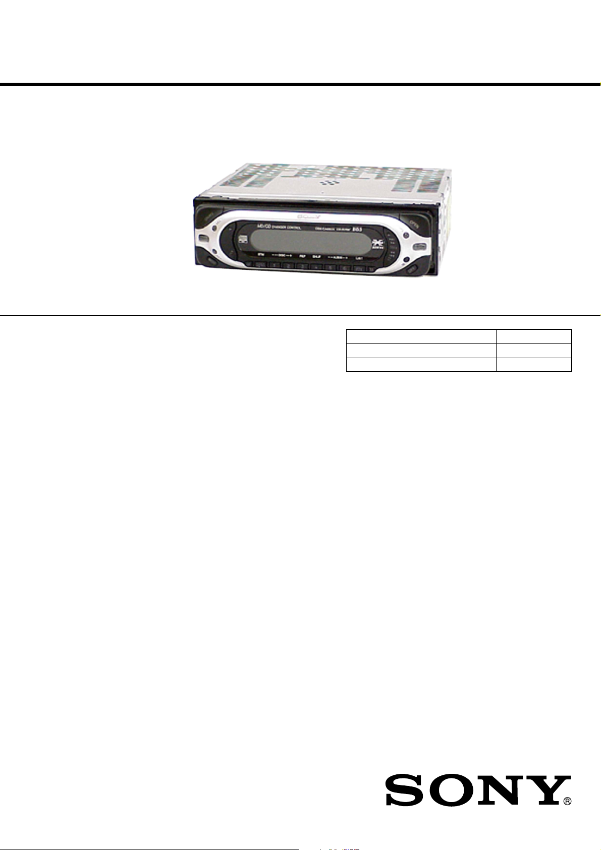
Photo: CDX-CA680X
• The tuner and CD sections have no adjustments.
SPECIFICATIONS
AEP Model
UK Model
Model Name Using Similar Mechanism CDX-L380X
CD Drive Mechanism Type MG-393XA-121//Q
Optical Pick-up Name KSS-720A
CD player section
Signal-to-noise ratio 90 dB
Frequency response 10 – 20,000 Hz
Wow and flutter Below measurable limit
Tuner section
FM
Tuning range 87.5 – 108.0 MHz
Aerial terminal External aerial connector
Intermediate frequency 10.7 MHz/450 kHz
Usable sensitivity 9 dBf
Selectivity 75 dB at 400 kHz
Signal-to-noise ratio 67 dB (stereo),
69 dB (mono)
Harmonic distortion at 1 kHz
0.5% (stereo),
0.3% (mono)
Separation 35 dB at 1 kHz
Frequency response 30 – 15,000 Hz
MW/LW
Tuning range MW: 531 – 1,602 kHz
LW: 153 – 279 kHz
Aerial terminal External aerial connector
Intermediate frequency 10.7 MHz/450 kHz
Sensitivity MW: 30 µV
LW: 40 µV
Power amplifier section
Outputs Speaker outputs
(sure seal connectors)
Speaker impedance 4 – 8 ohms
Maximum power output 50 W × 4 (at 4 ohms)
General
Outputs Audio outputs (front)
(CDX-CA680X only)
Audio outputs (rear)
Power aerial relay control
terminal
Power amplifier control
terminal
Inputs Telephone ATT control
terminal
Remote controller input
terminal
BUS control input terminal
(CDX-CA680X only)
BUS audio input terminal
(CDX-CA680X only)
Tone controls Low ±10 dB at 60 Hz
(XPLOD)
Mid ±10 dB at 1 kHz
(XPLOD)
High ±10 dB at 10 kHz
(XPLOD)
Power requirements 12 V DC car battery
(negative ground)
Dimensions Approx. 178 × 50 × 180 mm
(w/h/d)
Mounting dimension Approx. 182 × 53 × 161 mm
(w/h/d)
Mass Approx. 1.2 kg
Supplied accessories Parts for installation and
connections
Front panel case (1)
Design and specifications are subject to change without
notice.
9-874-248-01
2002K0400-1
© 2002. 11
FM/MW/LW COMPACT DISC PLAYER
Sony Corporation
e Vehicle Company
Published by Sony Engineering Corporation
1
CDX-CA680X/L580X
SERVICE NOTES
This label is located on the bottom of the chassis.
This label is located on the drive unit’s internal chassis.
When replacing the chassis (T.U) of mechanism deck which have
the “CAUTION LABEL” attached, please be sure to put a new
LABEL (OP CAUTION) (3-223-913-01) to the chassis (T.U).
NOTES ON HANDLING THE OPTICAL PICK-UP BLOCK
OR BASE UNIT
The laser diode in the optical pick-up block may suffer electrostatic
breakdown because of the potential difference generated by the
charged electrostatic load, etc. on clothing and the human body.
During repair, pay attention to electrostatic breakdown and also use
the procedure in the printed matter which is included in the repair
parts.
The flexible board is easily damaged and should be handled with
care.
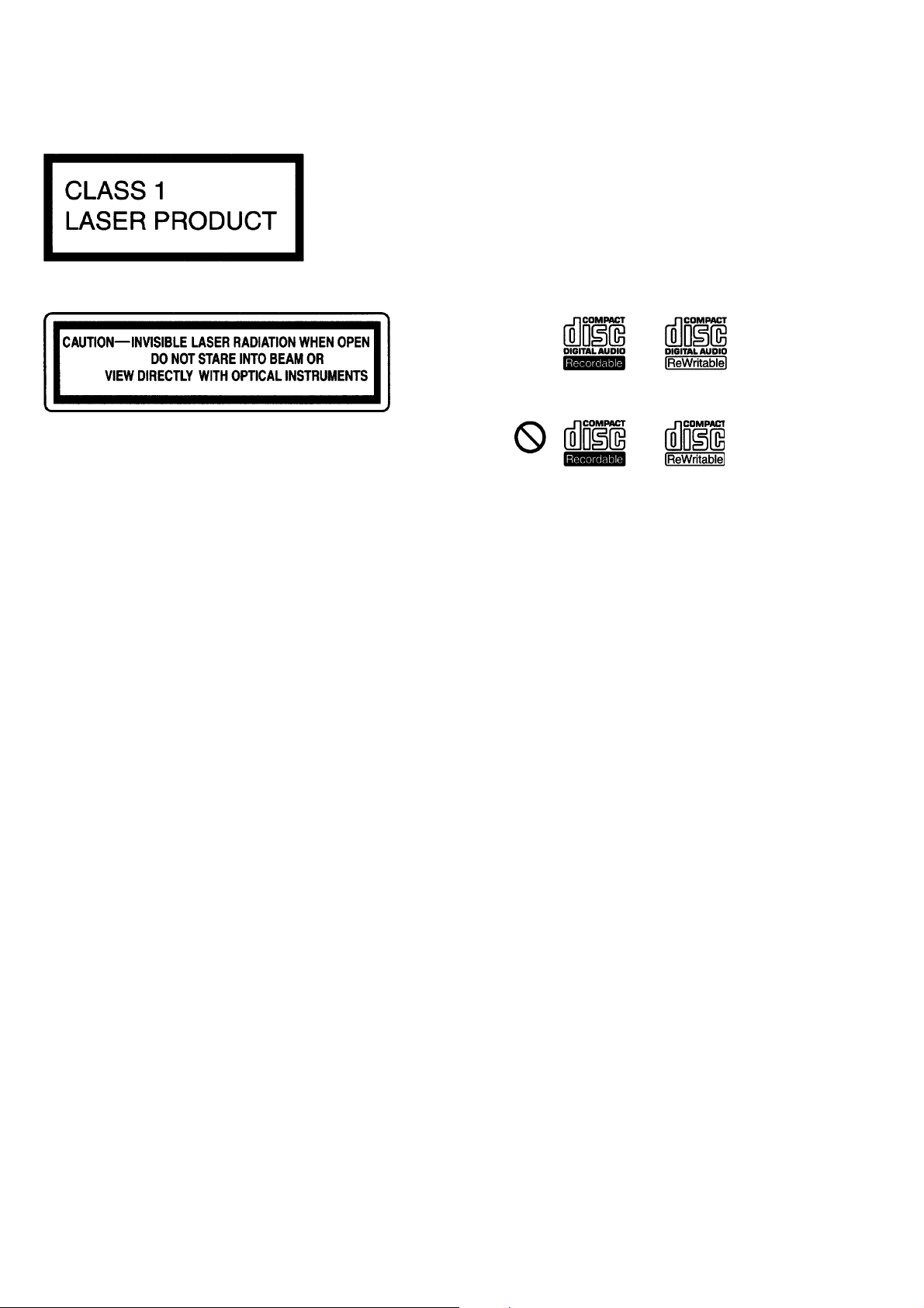
TEST DISCS
This set can playback CD-R and CD-ROM discs. The following
test discs should be used to check the capability:
CD-R test disc TCD-R082LMT (Part No. J-2502-063-1)
CD-RW test disc TCD-W082L (Part No. J-2502-063-2)
Notes on CD-R/CD-RW discs
•You can play CD-Rs (recordable CDs)/CD-RWs (re writable CDs)
designed for audio use on this unit.
Look for these marks to distinguish CD-Rs/CD-RWs for audio
use.
These marks denote that a disc is not for audio use.
• Some CD-Rs/CD-RWs (depending on the equipment used for
its recording or the condition of the disc) may not play on this
unit.
•You cannot play a CD-R/a CD-RW that is not finalized*.
*A process necessary for a recorded CD-R/CD-RW disc to be
played on the audio CD player.
NOTES ON LASER DIODE EMISSION CHECK
The laser beam on this model is concentrated so as to be focused on
the disc reflective surface by the objective lens in the optical pickup block. Therefore, when checking the laser diode emission, observe from more than 30 cm away from the objective lens.
Notes on Chip Component Replacement
• Never reuse a disconnected chip component.
• Notice that the minus side of a tantalum capacitor may be dam-
aged by heat.
SAFETY-RELATED COMPONENT WARNING!!
COMPONENTS IDENTIFIED BY MARK 0 OR DOTTED LINE
WITH MARK 0 ON THE SCHEMATIC DIAGRAMS AND IN
THE PARTS LIST ARE CRITICAL TO SAFE OPERATION.
REPLACE THESE COMPONENTS WITH SONY P ARTS WHOSE
PART NUMBERS APPEAR AS SHOWN IN THIS MANUAL OR
IN SUPPLEMENTS PUBLISHED BY SONY.
2
z
UNLEADED SOLDER
Boards requiring use of unleaded solder are printed with the lead
free mark (LF) indicating the solder contains no lead.
(Caution: Some printed circuit boards may not come printed with
the lead free mark due to their particular size.)
: LEAD FREE MARK
Unleaded solder has the following characteristics.
• Unleaded solder melts at a temperature about 40°C higher than
ordinary solder.
Ordinary soldering irons can be used but the iron tip has to be
applied to the solder joint for a slightly longer time.
Soldering irons using a temperature regulator should be set to
about 350°C.
Caution: The printed pattern (copper foil) may peel away if the
heated tip is applied for too long, so be careful!
• Strong viscosity
Unleaded solder is more viscous (sticky, less prone to flow)
than ordinary solder so use caution not to let solder bridges
occur such as on IC pins, etc.
• Usable with ordinary solder
It is best to use only unleaded solder but unleaded solder may
also be added to ordinary solder.
CDX-CA680X/L580X
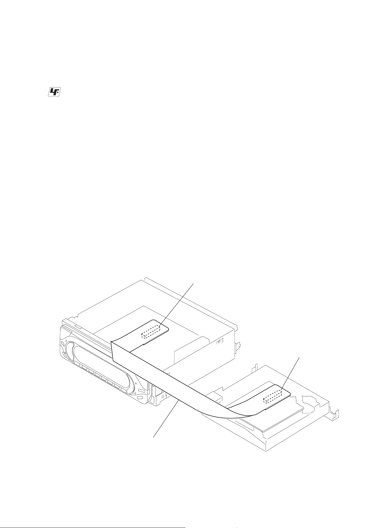
EXTENSION CABLE AND SERVICE POSITION
When repairing or servicing this set, connect the jig (extension cable)
as shown below.
• Connect the MAIN board (CNP301) and the SER V O board (CN1)
with the extension cable (Part No. J-2502-011-1).
MAIN BOARD
CNP301
SERVO BOARD
CN1
J-2502-011-1
3

CDX-CA680X/L580X
TABLE OF CONTENTS
1. GENERAL
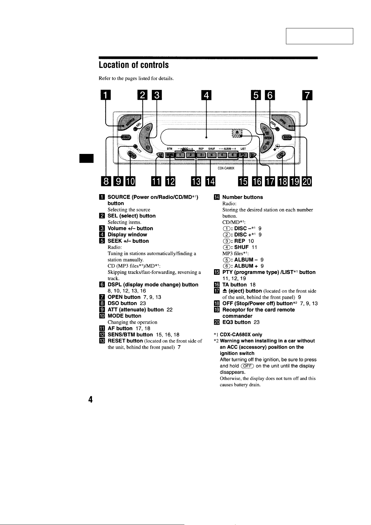
Location of controls................................................................. 5
Connections .............................................................................6
2. DISASSEMBLY
2-1. Sub Panel Assy.................................................................... 7
2-2. CD Mechanism Block ......................................................... 8
2-3. Main Board ......................................................................... 8
2-4. Heat Sink ............................................................................. 9
2-5. Chassis (T.U) Assy .............................................................. 9
2-6. Disc in Board .................................................................... 10
2-7. Servo Board....................................................................... 10
2-8. Shaft Roller Assy .............................................................. 11
2-9. Floating Block Assy .......................................................... 11
2-10. Optical Pick-up Block ....................................................... 12
3. DIAGRAMS
3-1. IC Pin Description............................................................. 13
3-2. Block Diagram –CD Section–........................................... 14
3-3. Block Diagram –Tuner Section–....................................... 15
3-4. Block Diagram –Display Section–.................................... 16
3-5. Circuit Boards Location .................................................... 17
3-6. Printed Wiring Boards –CD Mechanism Section–............ 18
3-7. Schematic Diagram –CD Mechanism Section– ................ 20
3-8. Printed Wiring Board –Main Section– .............................. 21
3-9. Schematic Diagram –Main Section (1/2)– ........................ 22
3-10. Schematic Diagram –Main Section (2/2)– ........................ 23
3-11. Printed Wiring Board –Relay Section– ............................. 24
3-12. Printed Wiring Board –Key Section– ................................ 25
3-13. Schematic Diagram –Key Section–...................................26
3-14. IC Block Diagrams............................................................ 27
4. EXPLODED VIEWS
4-1. Chassis Section ................................................................. 29
4-2. Main Board Section .......................................................... 30
4-3. Front Panel Section ........................................................... 31
4-4. CD Mechanism Section (1) ............................................... 32
4-5. CD Mechanism Section (2) ............................................... 33
4-6. CD Mechanism Section (3) ............................................... 34
5. ELECTRICAL PARTS LIST ........................................ 35
4
SECTION 1
GENERAL
CDX-CA680X/L580X
This section is extracted
from instruction manual.
5
CDX-CA680X/L580X
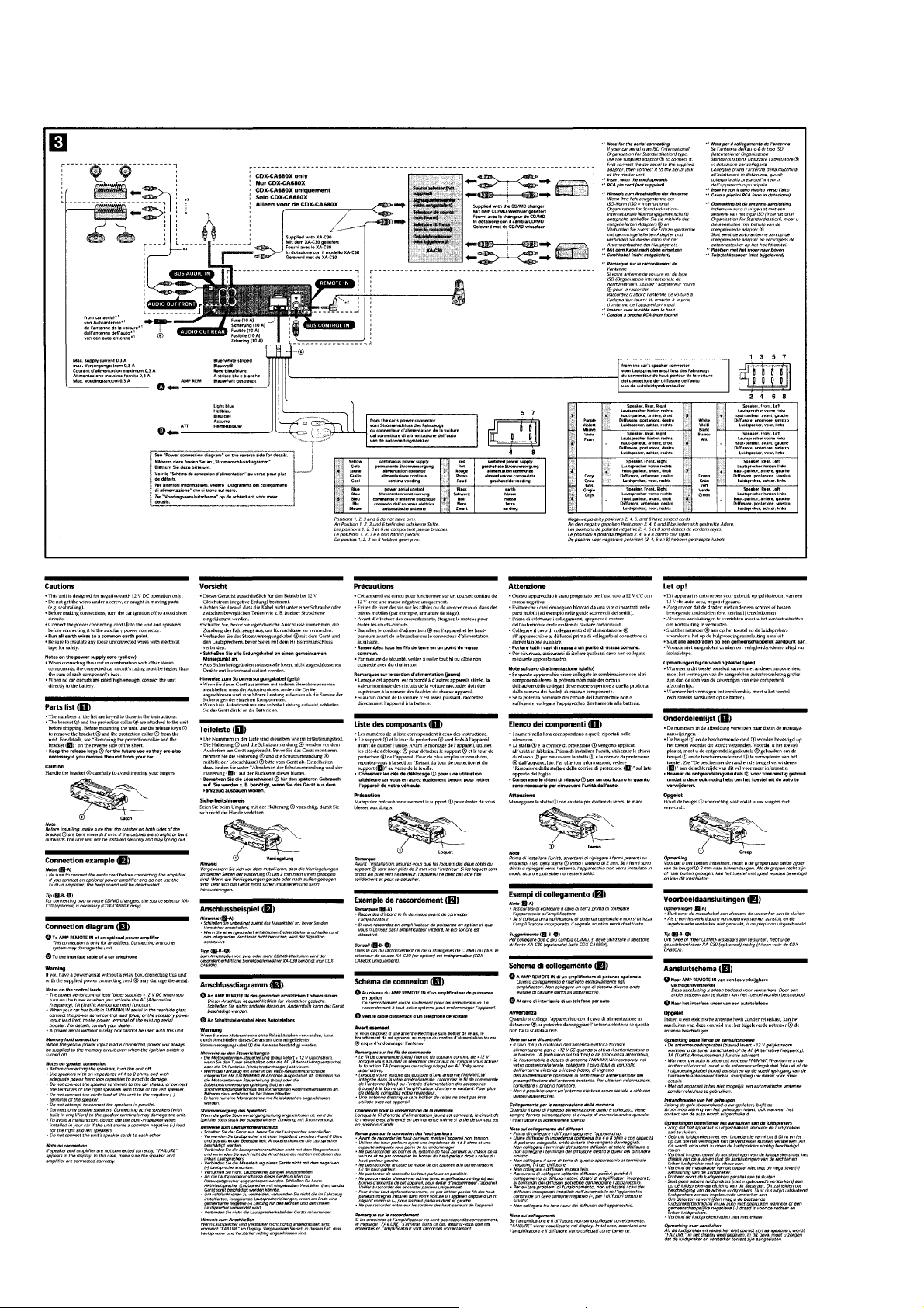
Connections
6
SECTION 2
DISASSEMBLY
Note : This set can be disassemble according to the following sequence.
SET
2-5. CHASSIS (T.U) ASSY
2-1. SUB PANEL ASSY
(Page 7)
(Page 9)
CDX-CA680X/L580X
2-2. CD MECHANISM BLOCK
(Page 8)
2-3. MAIN BOARD
(Page 8)
2-4. HEAT SINK
(Page 9)
2-6. DISC IN BOARD
(Page 10)
2-8. SHAFT ROLLER ASSY
(Page 11)
2-9. FLOATING BLOCK ASSY
(Page 11)
2-10. OPTICAL PICK-UP BLOCK
(Page 12)
Note : Follow the disassembly procedure in the numerical order given.
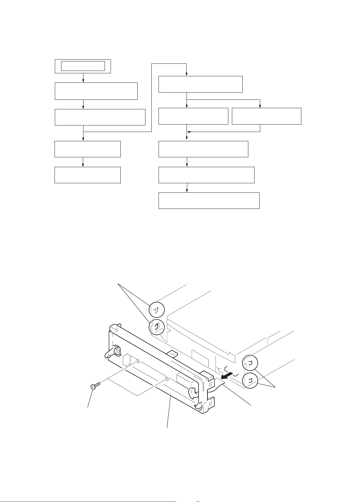
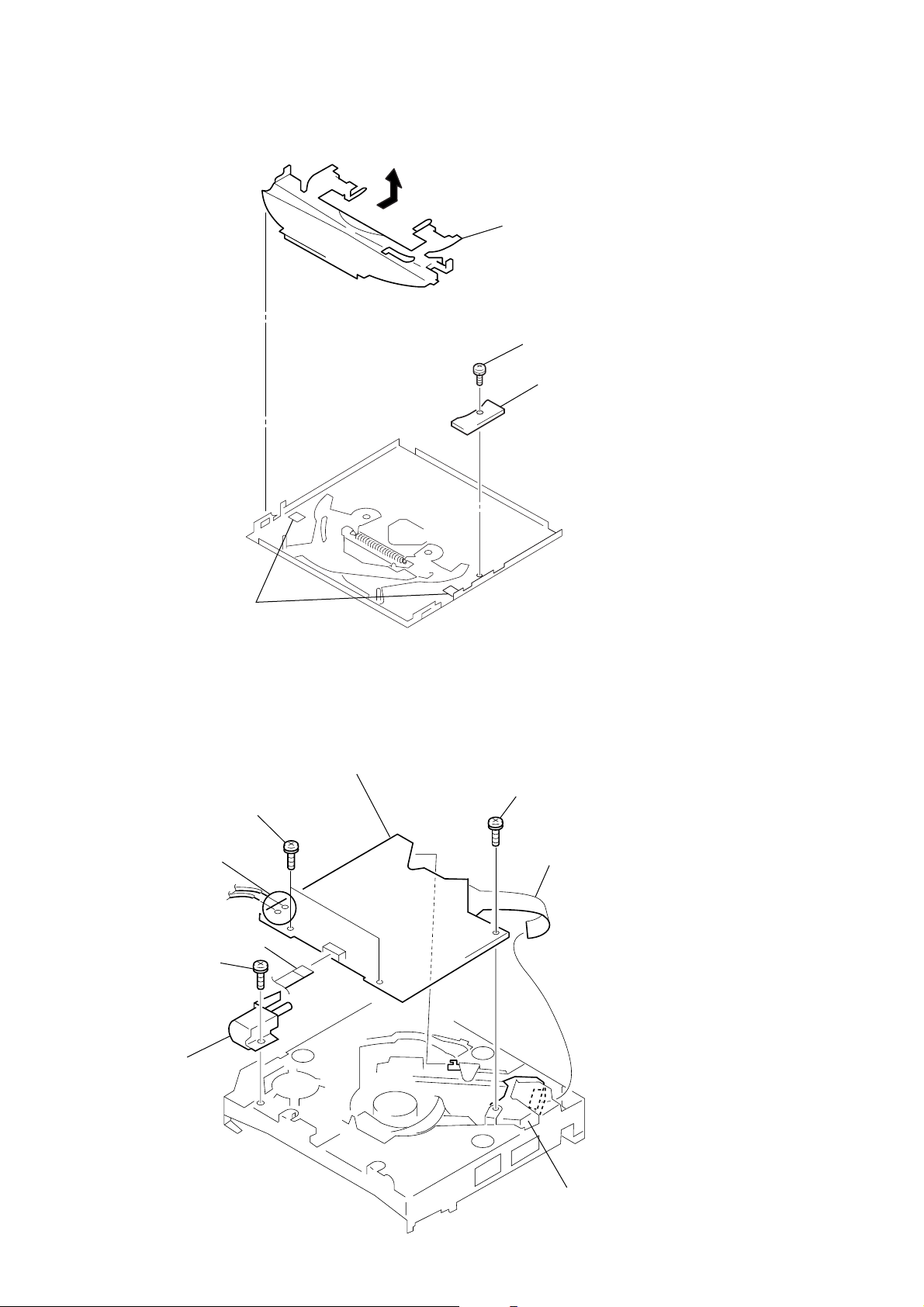
2-1. SUB PANEL ASSY
2
claws
2-7. SERVO BOARD
(Page 10)
1
PTT 2.6x6
5
sub panel assy
4
CN702
3
claws
7
CDX-CA680X/L580X
4
6
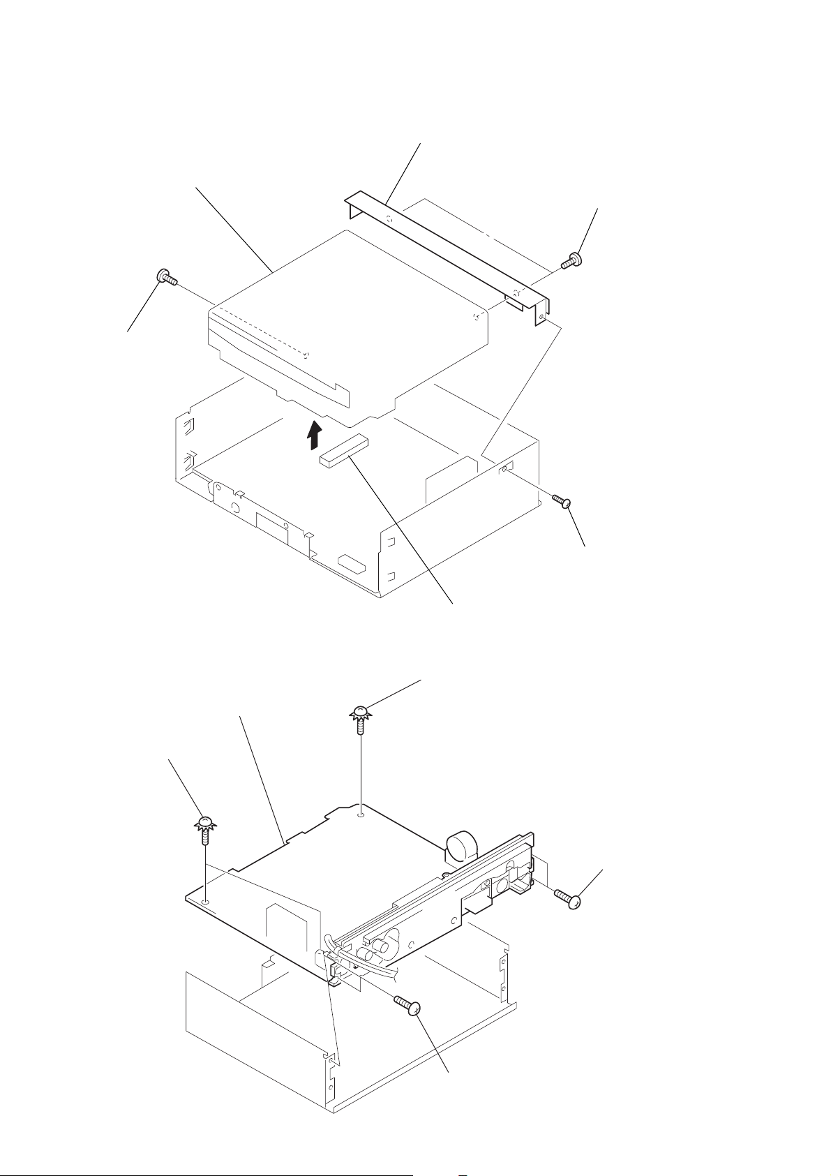
2-2. CD MECHANISM BLOCK
5
CD mechanism block
2
PTT 2.6x6
7
bracket (CD)
6
PTT 2.6x
2-3. MAIN BOARD
4
PTT 2.6x6
(ground point)
5
MAIN board
3
4
CNP301
3
PTT 2.6x6
(ground point)
1
PTT 2.6x6
1
PTT 2.6x
2
PTT 2.6x6
8
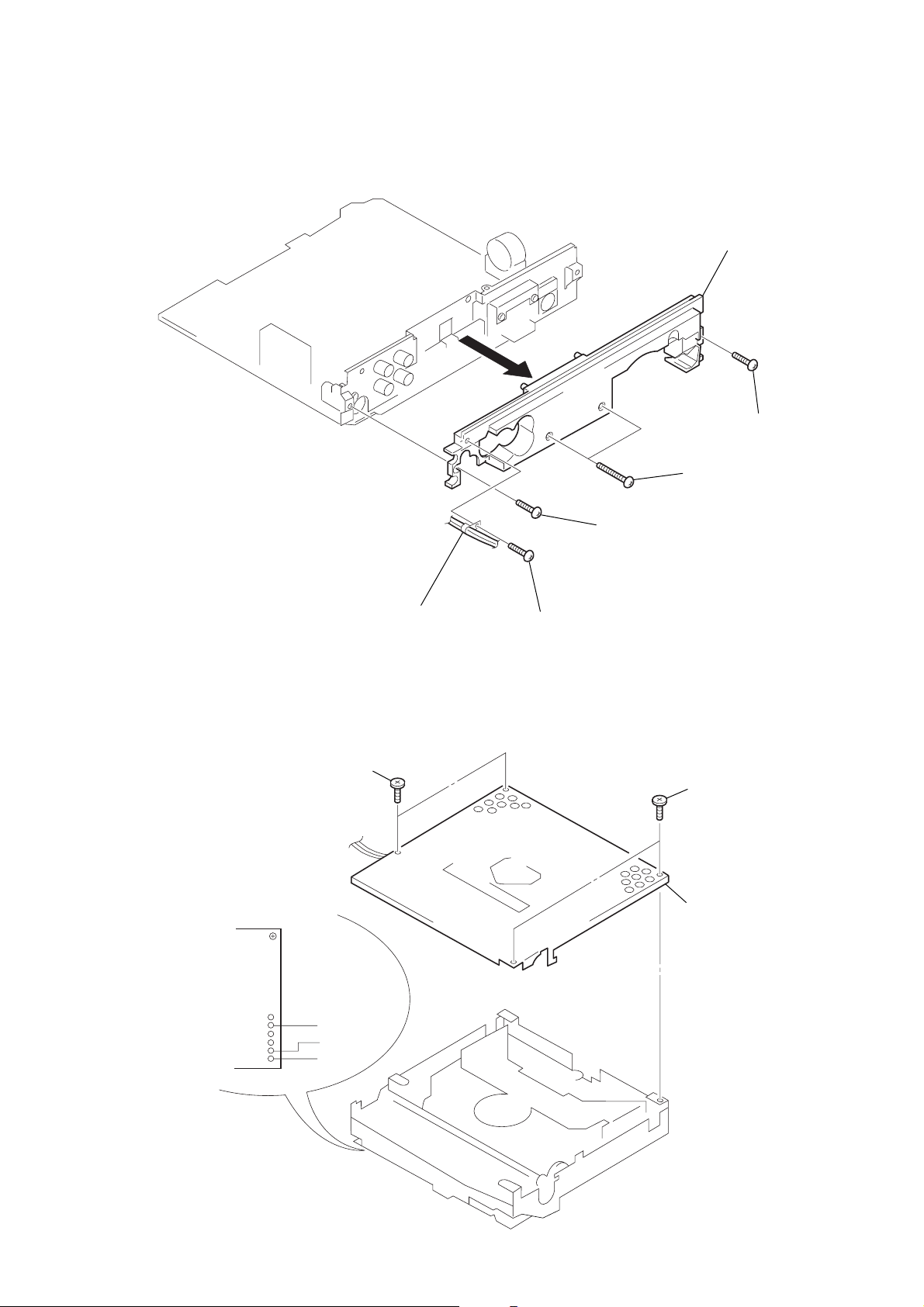
2-4. HEAT SINK
8
6
CDX-CA680X/L580X
7
heat sink
5
PTT 2.6x
4
PTT 2.6x12
2-5. CHASSIS (T.U) ASSY
1
Unsolder the
lead wires.
2
P 2x3
2
cord (RCA)
1
PTT 2.6x8
3
PTT 2.6x8
3
P 2x3
4
chassis (T.U) assy
black
red
white
9
CDX-CA680X/L580X
2-6. DISC IN BOARD
4
guide (disc)
1
PS 2x3
2
DISC IN board
2-7. SERVO BOARD
2
Removal the solders.
3
P 2x3
3
claws
5
PS 2x4
1
CN3
7
SERVO board
6
PS 2x4
8
PICK-UP FLEXIBLE board
10
4
loading motor assy
optical pick-up block
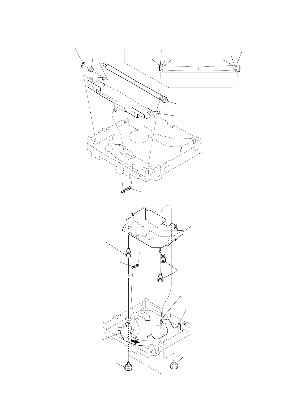
2-8. SHAFT ROLLER ASSY
• When installing, take note of the positions
arm (roller) and washers. (Fig. 1)
3
retaining ring (roller)
4
bearing (roller)
bearing (roller)
retaining ring (roller)
washer (RA)
arm
Fig. 1
5
shaft roller assy
2
arm (roller T)
CDX-CA680X/L580X
bearing (roller)
washer (RA)
arm
2-9. FLOATING BLOCK ASSY
8
compression spring (FL)
1
tension spring (KF1)
1
tension spring (RA3)
7
floating block assy
9
compression spring (FL)
2
tension spring (KR1)
5
Fit lever (D) in the
direction of the arrow.
6
Turn loading ring in the
direction of the arrow.
4
damper (T)
3
damper (T)
11
CDX-CA680X/L580X
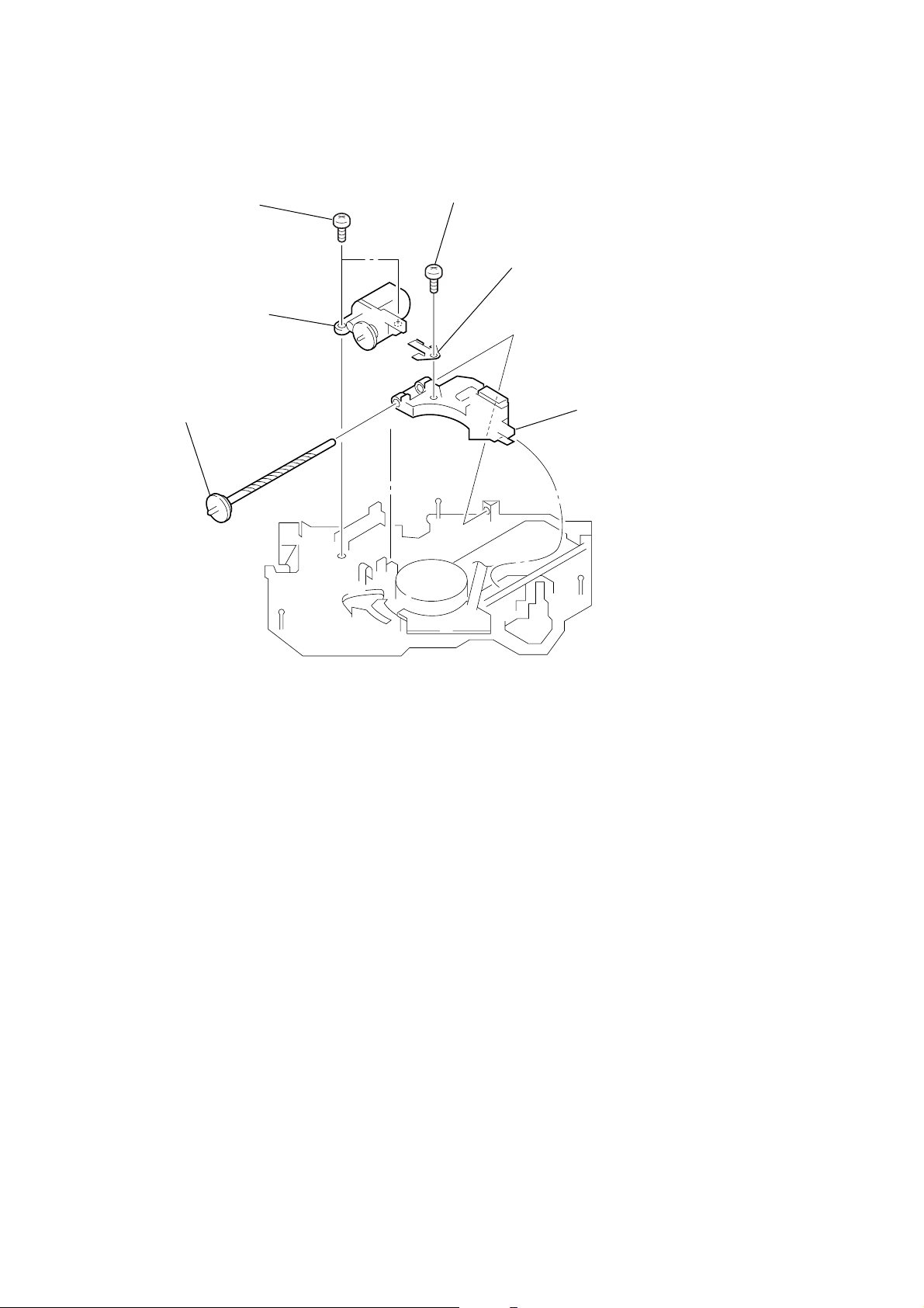
2-10. OPTICAL PICK-UP BLOCK
1
P 2x3
2
sled motor assy
6
shaft (feed) assy
4
P 2x3
5
leaf spring (feed)
3
optical pick-up block
12
CDX-CA680X/L580X
SECTION 3
DIAGRAMS
3-1. IC PIN DESCRIPTION
• IC501 MN101C49KSE (SYSTEM CONTROL)
Pin No. Pin Name I/O Pin Description
1VREF– — A/D converter power supply (–) pin
2 VSM I S-meter voltage detection input
3QUALITY I Noise detection input
4, 5 KEYIN1, 0 I Key input 1, 0
6 RCIN0 I Rotary commander key input
7 – 9 NIL I Not used. (Fixed at L in this set)
10 VREF+ — A/D converter power supply (+) pin (+5 V)
11 VDD — Power supply pin (+5 V)
12 OSCOUT O Main clock output (18.432 MHz)
13 OSCIN I Main clock input (18.432 MHz)
14 VSS — Ground
15 XIN I Sub clock input (32.768 kHz)
16 XOUT O Sub clock output (32.768 kHz)
17 MMOD I Not used. (Fixed at L in this set)
18 LCDSO O Serial data output for LCD driver IC.
19 LCDCE O Chip enable output for LCD driver IC.
20 LCDCKO O Serial clock output for LCD driver IC.
21 CD_TSO O Serial data output for CD servo IC.
22 CD_TSI I Serial data input from CD servo IC.
23 CD_TCKO O Serial clock output for CD servo IC.
24 SYSRST O System reset output (Used for CDX-CA680X only)
25 BUSON O BUS ON output (Used for CDX-CA680X only)
26 KEYACK I Key acknowledge detection input
27 DAVN I RDS data block synchronization detection input
28 BUIN I Backup power supply input
29 SIRCS I SIRCS input
30 TU_ATTIN I Tuner attenuator control input
31 CD_PACK I CD text pack synchronization signal input from CD servo IC.
32 NC (VCC) — Power supply pin (+5 V)
33 RESET I Microcomputer reset input
34 NOSE-SW I Front panel attachment detection input
35 BEEP O Beep output
36 NC O Not used. (Open)
37 TESTIN I Test mode detection input
38 ACCIN I Accessory power supply detection input
39 NC O Not used. (Open)
40 TELATT I Telephone attenuator detection input
41 NC (VCC) I Not used. (Fixed at H in this set)
42 UNISO O SONY-BUS data output (Used for CDX-CA680X only)
43 UNISI I SONY-BUS data input (Used for CDX-CA680X only)
44 UNICKO O SONY-BUS clock output (Used for CDX-CA680X only)
45 I2C_SIO I/O I2C BUS serial data input/output
46 NC O Not used. (Open)
47 I2C_CKO O I2C BUS serial clock output
48, 49 NC O Not used. (Open)
50 CD_SELFSW I CD mechanism deck Self switch detection input
51 TSTB O CD text parameter strobe output for CD servo IC.
52 RFOK I RFOK signal input from CD servo IC.
53 CD_RST O Reset signal output for CD servo IC.
54 A0 O Command/parameter discrimination signal output for CD servo IC.
55 STB O Data strobe signal output for CD servo IC.
13
 Loading...