

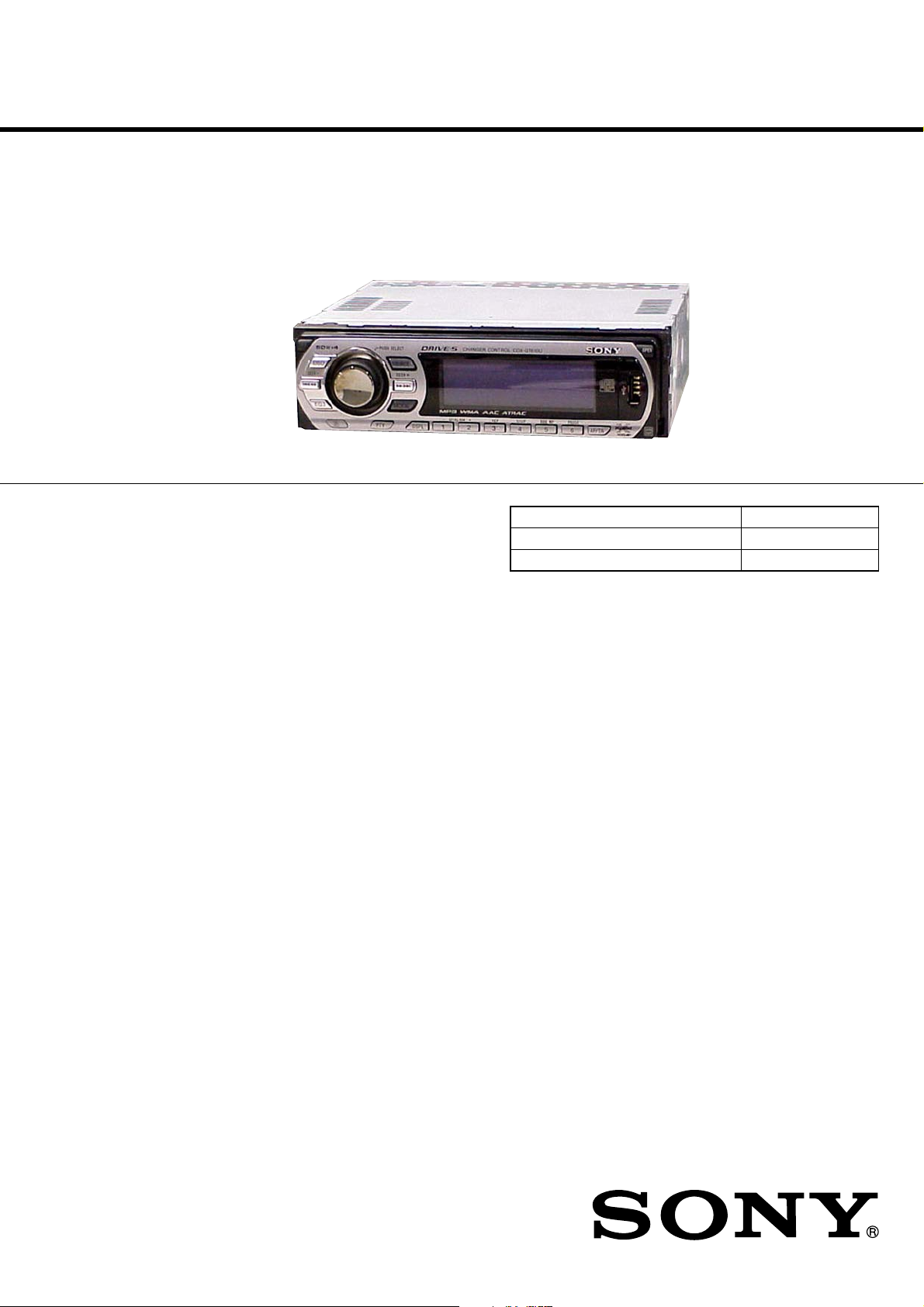
CDX-GT610U/GT616U/
GT617UE
SERVICE MANUAL
Ver. 1.1 2007.03
(Photo: CDX-GT610U)
• The tuner and CD sections have no adjustments.
SPECIFICATIONS
CD player section
Signal-to-noise ratio 120 dB
Frequency response 10 – 20,000 Hz
Wow and flutter Below measurable limit
Tuner section
FM
Tuning range CDX-GT610U/GT616U:
87.5 – 108.0 MHz
CDX-GT617UE:
FM1/FM2: 87.5 – 108.0 MHz (at 50 kHz step)
FM3: 65 – 74 MHz (at 30 kHz step)
Antenna terminal External antenna connector
Intermediate frequency 10.7 MHz/450 kHz
Usable sensitivity 9 dBf
Selectivity 75 dB at 400 kHz
Signal-to-noise ratio 67 dB (stereo), 69 dB (mono)
Harmonic distortion at 1 kHz
0.5% (stereo), 0.3% (mono)
Separation 35 dB at 1 kHz
Frequency response 30 – 15,000 Hz
AEP Model
UK Model
CDX-GT610U/GT616U
East European Model
CDX-GT617UE
Model Name Using Similar Mechanism CDX-GT410U/GT414U
CD Drive Mechanism Type MG-101U-188//Q
Optical Pick-up Name DAX-25A
MW/LW
Tuning range MW: 531 – 1,602 kHz
LW: 153 – 279 kHz
Antenna terminal External antenna connector
Intermediate frequency 10.7 MHz/450 kHz
Sensitivity MW: 30 µV, LW: 40 µV
USB player section
Interface USB (Full-speed)
Maximum current 500 mA
Power amplifier section
Outputs Speaker outputs (sure seal connectors)
Speaker impedance 4 – 8 ohms
Maximum power output
50 W × 4 (at 4 ohms)
– Continued on next page –
9-887-473-02
2007C04-1
© 2007.03
FM/MW/LW COMPACT DISC PLAYER
Sony Corporation
eVehicle Division
Published by Sony Techno Create Corporation
CDX-GT610U/GT616U/GT617UE
General
Outputs Audio outputs terminal (front/rear)
Inputs Telephone ATT control terminal
Tone controls Low: ±10 dB at 60 Hz (XPLOD)
Power requirements 12 V DC car battery (negative ground)
Dimensions Approx. 178 × 50 × 180 mm
Mounting dimensions Approx. 182 × 53 × 162 mm
Mass Approx. 1.3 kg (3 lb. 5 oz.)
Supplied accessories Card remote commander: RM-X151
Design and specifications are subject to change without
notice.
US and foreign patents licensed from Dolby Laboratories.
Subwoofer output terminal (mono)
Power antenna relay control terminal
Power amplifier control terminal
Illumination control terminal
BUS control input terminal
BUS audio input terminal/AUX IN terminal
Remote controller input terminal
Antenna input terminal
Mid: ±10 dB at 1 kHz (XPLOD)
High: ±10 dB at 10 kHz (XPLOD)
(7
1/8 × 2 × 7 1/8 in.) (w/h/d)
(7 1/4 × 2 1/8 × 6 1/2 in.) (w/h/d)
Parts for installation and connections (1 set)
SERVICE NOTES
Notes on Chip Component Replacement
•Never reuse a disconnected chip component.
• Notice that the minus side of a tantalum capacitor may be damaged
by heat.
TEST DISCS
Please use the following test discs for the check on the CD section.
YDES-18 (Part No. 3-702-101-01)
PATD-012 (Part No. 4-225-203-01)
CAUTION
Use of controls or adjustments or performance of procedures
other than those specified herein may result in hazardous
radiation exposure.
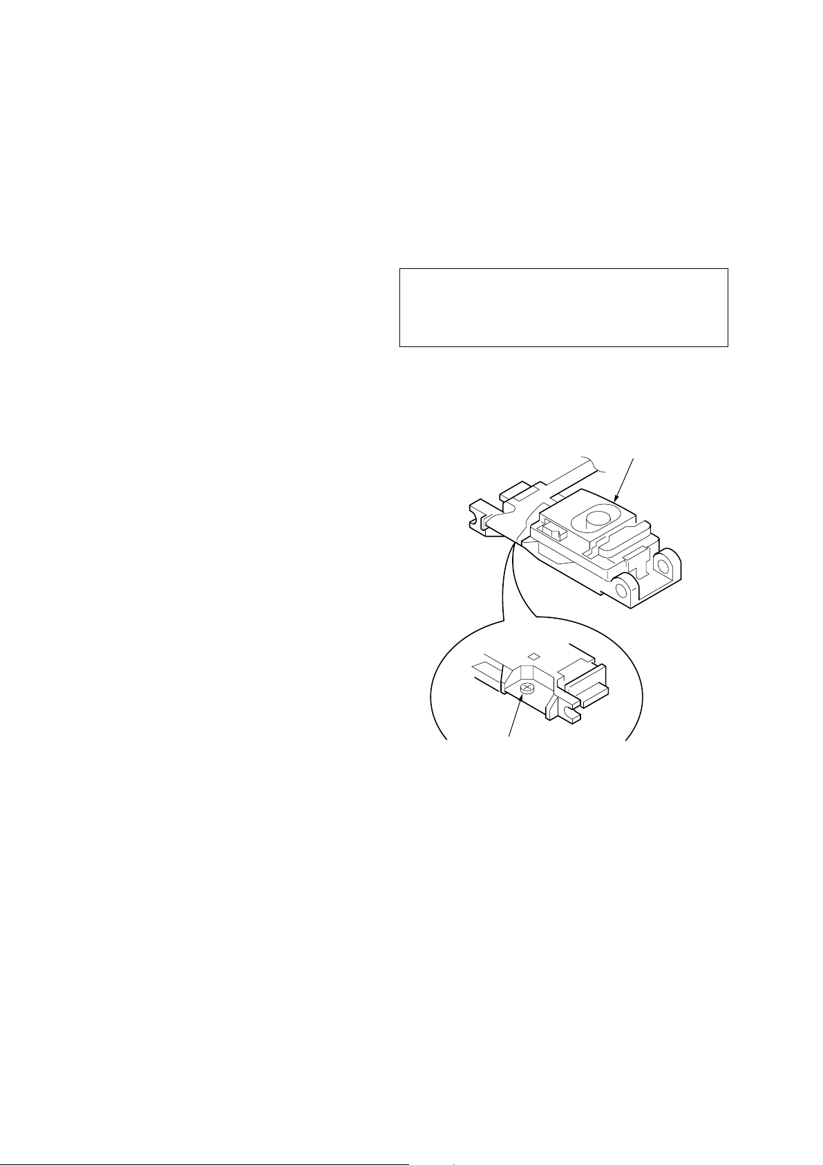
If the optical pick-up block is defective, please replace the whole
optical pick-up block.
Never turn the semi-fix ed resistor located at the side of optical pickup block.
optical pick-up
NOTES ON HANDLING THE OPTICAL PICK-UP BLOCK
OR BASE UNIT
The laser diode in the optical pick-up block may suffer electrostatic
breakdown because of the potential difference generated by the
charged electrostatic load, etc. on clothing and the human body.
During repair, pay attention to electrostatic breakdown and also use
the procedure in the printed matter which is included in the repair
parts.
The flexible board is easily damaged and should be handled with
care.
NOTES ON LASER DIODE EMISSION CHECK
The laser beam on this model is concentrated so as to be focused on
the disc reflective surface by the objective lens in the optical pickup block. Therefore, when checking the laser diode emission,
observe from more than 30 cm away from the objective lens.
semi-fixed resistor
SAFETY-RELATED COMPONENT WARNING!!
COMPONENTS IDENTIFIED BY MARK 0 OR DOTTED LINE
WITH MARK 0 ON THE SCHEMATIC DIAGRAMS AND IN
THE PARTS LIST ARE CRITICAL TO SAFE OPERATION.
REPLACE THESE COMPONENTS WITH SONY PARTS
WHOSE PART NUMBERS APPEAR AS SHOWN IN THIS
MANUAL OR IN SUPPLEMENTS PUBLISHED BY SONY.
2
CDX-GT610U/GT616U/GT617UE
D
This compact disc player is classified as a CLASS 1 LASER
product. The CLASS 1 LASER PRODUCT label is located on the
exterior.
This label is located on the bottom of the chassis.
• CD playback
You can play CD-DA (also containing CD TEXT*), CD-R/CDRW (MP3/WMA/AAC files also containing Multi Session) and
ATRAC CD (ATRAC3 and ATRAC3plus format).
Type of discs Label on the disc
CD-DA
MP3
WMA
AAC
ATRAC CD
UNLEADED SOLDER
•
Boards requiring use of unleaded solder are printed with the leadfree mark (LF) indicating the solder contains no lead.
(Caution:Some printed circuit boards may not come printed with
the lead free mark due to their particular size.)
: LEAD FREE MARK
Unleaded solder has the following characteristics.
• Unleaded solder melts at a temperature about 40°C higher than
ordinary solder.
Ordinary soldering irons can be used but the iron tip has to be
applied to the solder joint for a slightly longer time.
Soldering irons using a temperature regulator should be set to
about 350°C.
Caution:The printed pattern (copper foil) may peel away if the
heated tip is applied for too long, so be careful!
• Strong viscosity
Unleaded solder is more viscous (sticky, less prone to flow)
than ordinary solder so use caution not to let solder bridges
occur such as on IC pins, etc.
• Usable with ordinary solder
It is best to use only unleaded solder but unleaded solder may
also be added to ordinary solder.
*A CD TEXT disc is a CD-DA that includes information such as
disc, artist and track name.
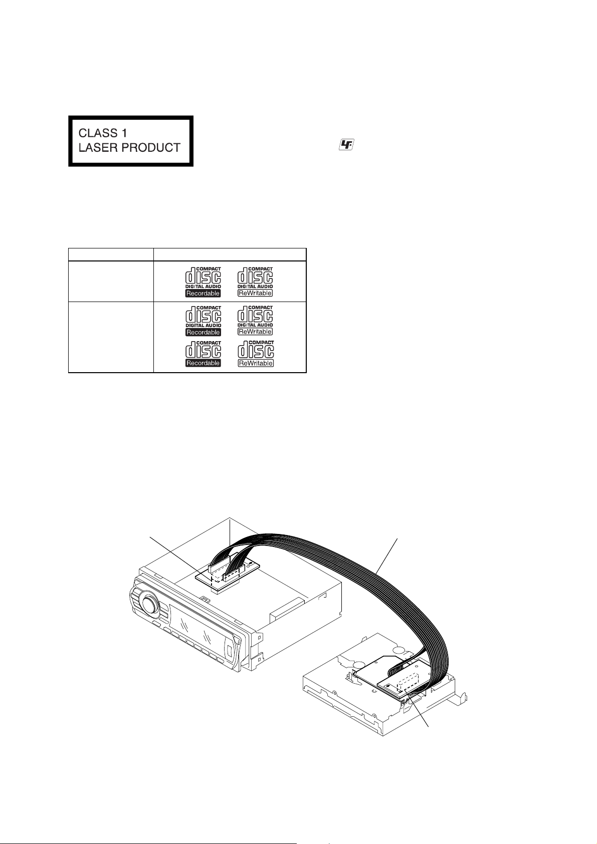
EXTENSION CABLE AND SERVICE POSITION
When repairing or servicing this set, connect the jig (extension cable)
as shown below.
• Connect the MAIN board (CN350) and the SER V O board (CN2)
with the extension cable (Part No. J-2502-076-1).
MAIN BOARD
CN350
J-2502-076-1
SERVO BOAR
CN2
3
CDX-GT610U/GT616U/GT617UE
d
Ver. 1.1
NOTE FOR REPLACEMENT OF THE SERVO BOARD
When repairing, the complete SER VO board (A-1206-357-A) should
be replaced since any parts in the SER V O board cannot be repaired.
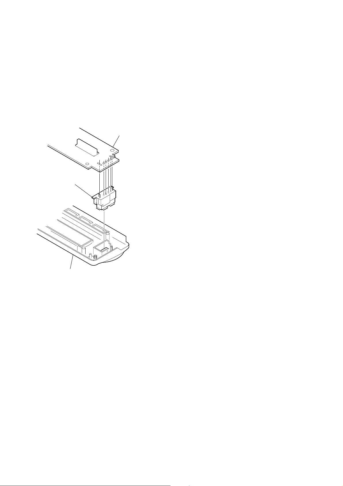
NOTE FOR REPLACEMENT OF THE USB CONNECTOR
(J11)
To replace the USB connector requires alignment.
1. Insert the USB connector into the front panel.
2. Place the KEY board on the front panel and align the terminals
of the USB connector with the holes in the KEY board.
3. Solder the four terminals of the connector.
KEY boar
USB (socket) connector
TABLE OF CONTENTS
1. GENERAL
Location of Controls........................................................ 5
Connections ..................................................................... 6
2. DISASSEMBLY
2-1. Sub Panel Assy ................................................................ 11
2-2. CD Mechanism Block ..................................................... 11
2-3. Main Board...................................................................... 12
2-4. Servo Board ..................................................................... 12
2-5. Chassis (T) Sub Assy....................................................... 13
2-6. Roller Arm Assy .............................................................. 13
2-7. Chassis (OP) Assy ........................................................... 14
3. DIAGNOSIS FUNCTION ........................................ 15
4. DIAGRAMS
4-1. Block Diagram –Main Section– ...................................... 19
4-2. Block Diagram –Display Section– .................................. 20
4-3. Printed Wiring Board –Main Section– ............................ 22
4-4. Schematic Diagram –Main Section (1/3)– ...................... 23
4-5. Schematic Diagram –Main Section (2/3)– ...................... 24
4-6. Schematic Diagram –Main Section (3/3)– ...................... 25
4-7. Printed Wiring Board –Sub Section– .............................. 26
4-8. Schematic Diagram –Sub Section– ................................. 27
4-9. Printed Wiring Board –Key Section– .............................. 28
4-10. Schematic Diagram –Key Section–................................. 29
front panel
NOTE FOR THE 20-PIN CONNECTOR (CN901)
Do not use alcohol to clean the 20-pin connector (CN901) connecting
the front panel with the main body.
Do not touch the connector directly with your bare hand. Poor contact
may be caused.
5. EXPLODED VIEWS
5-1. Main Section.................................................................... 33
5-2. Front Panel Section ......................................................... 34
5-3. CD Mechanism Section (MG-101U-188//Q) .................. 35
6. ELECTRICAL PARTS LIST.................................. 36
4
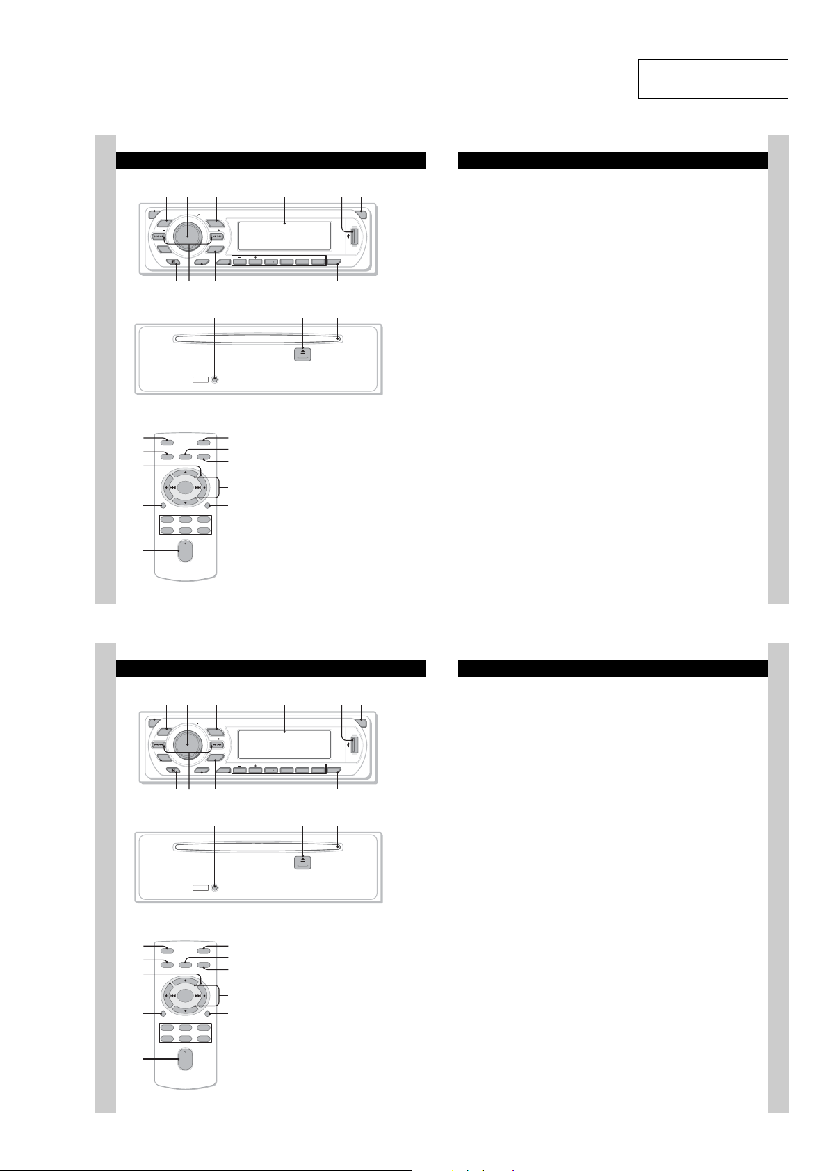
• LOCATION OF CONTROLS
q;9 qaq
q
q
q
8
• CDX-GT610U/GT616U
Location of controls and basic operations
Main unit
1
2
OFF
DSO
SEEK SEEK
EQ3
8
Front panel removed
Card remote commander
RM-X151
1
OFF
4
SOURCE
ql
DSPL
qd
132
465
w;
6
3
PUSH SELECT
PTY
9 qa qd qgqs
q;
RESET
ATT
SEL
MODE
+
–
SCRL
+
VOL
–
4 5
SOURCE
MODE
GP/ALBM
DSPL AF/TA
REP SHUF
123456
Refer to the pages listed for details. The
corresponding buttons on the card remote
commander control the same functions as those
on the unit.
wa
A OFF button
ws
B DSO button 4
qs
wd
C Volume control dial/select button 12
wf
D SOURCE button
wg
E Display window
F USB terminal 11
G OPEN button 5
67
OPEN
PAUSE
BBE MP
CDX-GT616U
qf
CDX-GT610U
qj qkqh
To po we r off; stop the source.
To se l e c t the DSO mode (1, 2, 3 or OFF).
The larger the number, the more enhanced
the effect.
To ad ju st vo lume (rotate); select setup items
(press and rotate).
To po we r on; change the sour ce (Radio/CD/
1
MD*
/USB/AUX).
To co nnect to the USB device.
SECTION 1
GENERAL
CDX-GT610U/GT616U/GT617UE
This section is extracted
from instruction manual.
H EQ3 (equalizer) button 12
To se le ct an equalizer type (XPLOD,
VOCAL, EDGE, CRUISE, SPACE,
GRAVITY, CUSTOM or OFF).
I Receptor for the card remote
commander
J SEEK –/+ buttons
1
CD/MD*
/USB*2:
To sk ip tracks (press); skip tracks
continuously (press, then press again within
about 1 second and hold); reverse/fastforward a track (press and hold).
Radio:
To tune in stations automatically (press); find
a station manually (press and ho ld).
K PTY (Program Type) button 10
To se le ct PTY in RDS.
L MODE button 8, 11, 13
To se le ct the radio band (FM/MW/LW);
3
select the unit*
M DSPL (display) button 8, 9, 11
To ch an g e display items.
N Number buttons
CD/MD*
(1)/(2): GP*
(3): REP 8, 11, 13
(4): SHUF 8, 11, 13
(5): BBE MP*
(6): PAUS E*
Radio:
To re ce ive stored stations (press); store
stations (press and hold).
O AF (Alternative Frequencies)/TA
(Traffic Announcement) button 9
To se t AF and TA in RDS.
P RESET button 4
Q Z (eject) button 5
To ej ect the disc.
R Disc slot 5
To in sert the disc.
; select the play mode*4.
1
/USB*2:
5
/ALBM*6 –/+
To s kip albums (press); skip albums
continuously (press and hold) .*
8
2
To a ct iv ate the BBE MP function, set
“BBE MP-ON.” To cancel, set “BBE
MP-OFF.”
8
To p ause playback. To cancel, press
again.
The following buttons on the card remote
commander have also different buttons/functions
from the unit. Remove the insulation film before
use (page 4).
ql < (.)/, (>) buttons
To control CD/radio/MD/USB, the same as
(SEEK) –/+ on the unit.
w; VOL (volume) +/– button
To adjust volume.
wa AT T (attenuate) button
To att e nuate the sound. To cancel, press
again.
ws SEL (select) button
The same as the select button on the unit.
wd M (+)/m (–) buttons
To control CD, the same as (1)/(2) (GP/
ALBM –/+) on the unit.
wf SCRL (scroll) button 8, 11
To s c roll the display item.
wg Number buttons
To r e c e ive stored stations (press); st ore
stations (press and hold).
*1
When an MD changer is connected.
*2
When a USB device is connected.
*3
When a CD/MD changer is connected.
*4
7
When an ATRAC Audio Device is connected.
*5
When an ATRAC CD is played.
*6
When an MP3/WMA/AAC is played.
*7
If the changer/USB is connected, the operation is
different, see page 13.
*8
When playing back on this unit and a USB device.
Notes
•
When ejecting/inserting a disc, keep any USB
devices disconnected to avoid damage to the disc.
•
If the unit is turned off and the display disappears, it
cannot be operated with the card remote
commander unless
pressed, or a disc is inserted to activate the unit first.
Tip
For details on how to replace the battery, see
“Replacing the lithium battery of the card remote
commander” on page 17.
About USB cap
When not using the USB terminal (
supplied USB cap to prevent dust or dirt entering.
Keep the USB cap out of the reach of children to
prevent accidental swallowing.
(SOURCE)
on the unit is
F
), use the
7
• CDX-GT617UE
Location of controls and basic operations
Main unit
1
2
OFF
DSO
SEEK SEEK
EQ3
Front panel removed
Card remote commander
RM-X151
1
OFF
4
SOURCE
ql
DSPL
qd
132
465
w;
6
4 5
PUSH SELECT
SOURCE
MODE
PTY
s
RESET
ATT
SEL
MODE
+
–
SCRL
+
VOL
–
GP/ALBM
DSPL AF/TA
REP SHUF
123456
d
PAUSE
BBE MP
f
qj qkqh
Refer to the pages listed for details. The
corresponding buttons on the card remote
commander control the same functions as those
on the unit.
wa
A OFF button
ws
qs
wd
wf
wg
To po we r off; stop the source.
B DSO button 4
To se l e c t the DSO mode (1, 2, 3 or OFF).
The larger the number, the more enhan ced
the effect.
C Volume control dial/select button 12
To ad ju st vo lume (rotate); select setup items
(press and rotate).
D SOURCE button
To po wer on; change the source (Radio/CD/
1
MD*
/USB/AUX).
E Display window
F USB terminal 11
To co nnect to the USB device.
G OPEN button 5
673
g
OPEN
CDX-GT617UE
H EQ3 (equalizer) button 12
To se le ct an equalizer type (XPLOD,
VOCAL, EDGE, CRUISE, SPACE,
GRAVITY, CUSTOM or OFF).
I Receptor for th e card remote
commander
J SEEK –/+ buttons
1
CD/MD*
/USB*2:
To sk ip tracks (press); skip tracks
continuously (press, then press again within
about 1 second and hold); reverse/fastforward a track (press and hold).
Radio:
To tune in stations automatically (press); find
a station manually (press and ho ld).
K PTY (Program Type) button 10
To se le ct PTY in RDS.
L MODE button 8, 11, 13
To se le ct the radio band (FM/MW/LW);
3
select the unit*
M DSPL (display) button 8, 9, 11
To ch an g e display items.
N Number buttons
CD/MD*
(1)/(2): GP*
(3): REP 8, 11, 13
(4): SHUF 8, 11, 13
(5): BBE MP*
(6): PAUS E*
Radio:
To re ce ive stored stations (press); store
stations (press and hold).
O AF (Alternative Frequencies)/TA
(Traffic Announcement) button 9
To se t AF and TA in RDS.
P RESET button 4
Q Z (eject) button 5
To ej ect the disc.
R Disc slot 5
To in sert the disc.
; select the play mode*4.
1
/USB*2:
5
/ALBM*6 –/+
To s kip albums (press); skip albums
continuously (press and hold) .*
8
2
To a ct iv ate the BBE MP function, set
“BBE MP-ON.” To cancel, set “BBE
MP-OFF.”
8
To p ause playback. To cancel, press
again.
The following buttons on the card remote
commander have also different buttons/functions
from the unit. Remove the insulation film before
use (page 4).
ql < (.)/, (>) buttons
To control CD/radio/MD/USB, the same as
(SEEK) –/+ on the unit.
w; VOL (volume) +/– button
To adjust volume.
wa AT T (attenuate) button
To att e nuate the sound. To cancel, press
again.
ws SEL (select) button
The same as the select button on the unit.
wd M (+)/m (–) buttons
To control CD, the same as (1)/(2) (GP/
ALBM –/+) on the unit.
wf SCRL (scroll) button 8, 11
To s c roll the display item.
wg Number buttons
To r e c e ive stored st at ions (press); store
stations (press and hold).
*1
When an MD changer is connected.
*2
When a USB device is connected.
*3
When a CD/MD changer is connected.
*4
7
When an ATRAC Audio Device is connected.
*5
When an ATRAC CD is played.
*6
When an MP3/WMA/AAC is played.
*7
If the changer/USB is connected, the operation is
different, see page 13.
*8
When playing bac k on this unit and a USB device.
Notes
•
When ejecting/inserting a disc, keep any USB
devices disconnected to avoid damage to the disc.
•
If the unit is turned off and the display disappears, it
cannot be operated with the card remote
commander unless
pressed, or a disc is inserted to activate the unit first.
Tip
For details on how to replace the battery, see
“Replacing the lithium battery of the card remote
commander” on page 17.
About USB cap
When not using the USB terminal (
supplied USB cap to prevent dust or dirt entering.
Keep the USB cap out of the reach of chil dren to
prevent accidental swallowing.
(SOURCE)
on the unit is
F
), use the
7
5
CDX-GT610U/GT616U/GT617UE
g
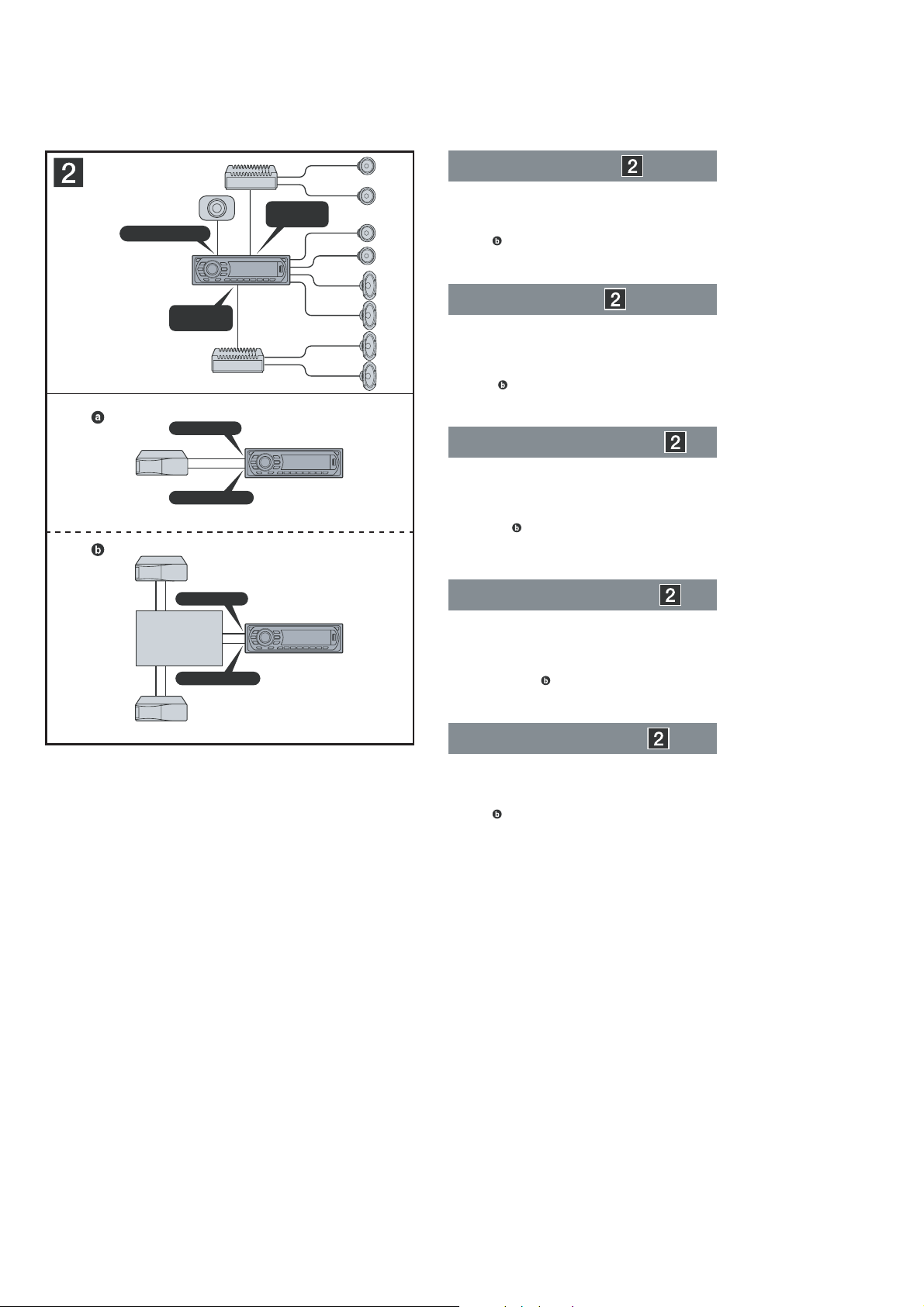
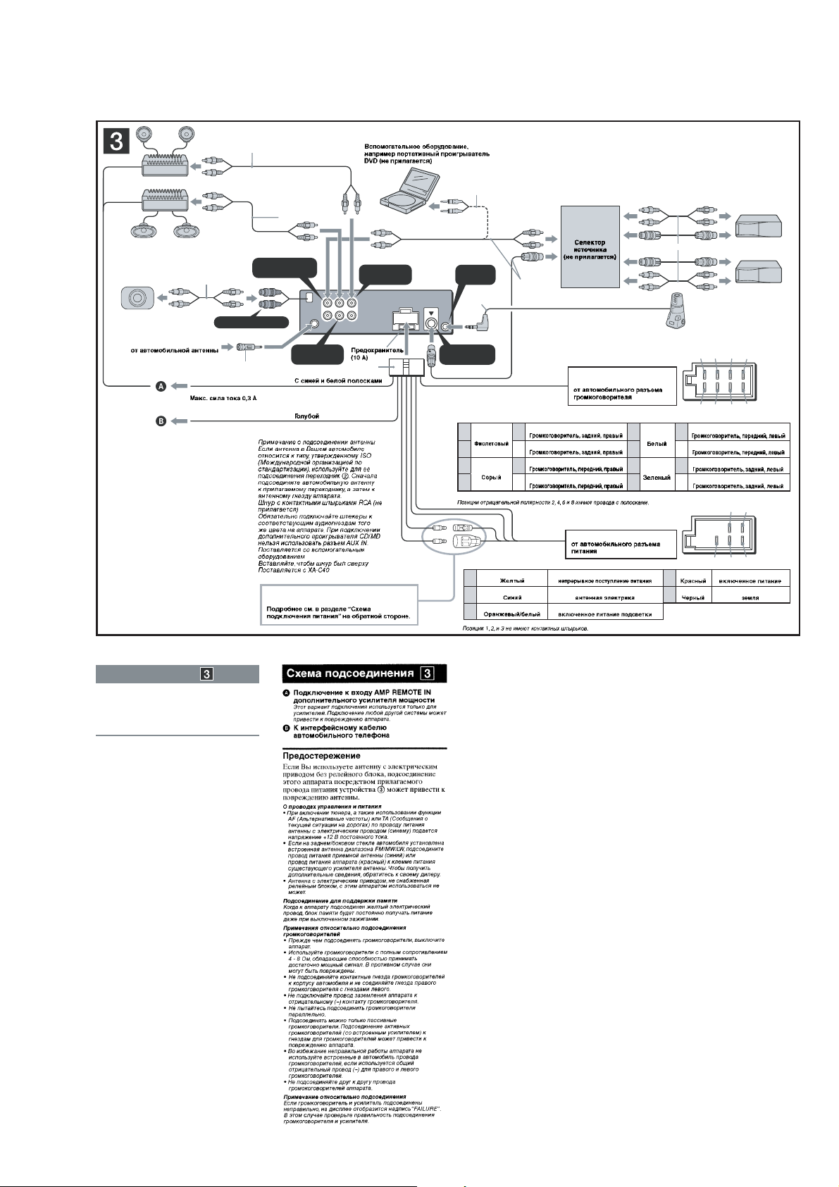
• CONNECTIONS
• CDX-GT610U/GT616U
A
SUB OUT (MONO)
AUDIO OUT
FRONT
Connection example
Notes
(2-A)
•
Be sure to connect the ground (earth) lead before connecting
the amplifi er.
•
The alarm will only sound if the built-in amplifi er is used.
Tip
(2-B-
For connecting two or more CD/MD changers, the source
selector XA-C40 (not supplied) is necessary.
)
B
AUDIO OUT
REAR
BUS AUDIO IN
BUS CONTROL IN
BUS AUDIO IN
Source selector*
Signalquellenwähler*
Sélecteur de source*
Selettore di fonte*
Geluidsbronkiezer*
XA-C40
BUS CONTROL IN
*
not supplied
nicht mitgeliefert
non fourni
non in dotazione
niet bijgeleverd
Anschlussbeispiel
Hinweise
(2-A)
•
Schließen Sie unbedingt zuerst das Massekabel an, bevor Sie
den Verstärker anschließen.
•
Der Warnton wird nur ausgegeben, wenn der integrierte
Verstärker verwendet wird.
Tipp
(2-B- )
Zum Anschließen von zwei oder mehr CD/MD-Wechslern wird
der Signalquellenwähler XA-C40 (nicht mitgeliefert) benötigt.
Exemple de raccordement
Remarques
•
•
Conseil
Dans le cas du raccordement de deux changeurs de CD/MD
ou plus, le sélecteur de source XA-C40 (non fourni) est
indispensable.
(2-A)
Raccordez d’abord le câble de mise à la masse avant de
connecter l’amplifi cateur.
L’alarme est émise uniquement lorsque l’amplifi cateur intégré
est utilisé.
(2-B- )
Esempio di collegamento
Note
(2-A)
•
•
Suggerimento
Per collegare due o più cambia CD/MD, occorre utilizzare il
selettore di fonte XA-C40 (non in dotazione).
Assicurarsi di collegare il cavo di terra prima di collegare
l’apparecchio all’amplifi catore.
L’allarme viene emesso solo se è in uso l’amplifi catore
incorporato.
(2-B- )
Voorbeeldaansluitingen
Opmerkingen
•
Sluit eerst de aarddraad aan voordat u de versterker aansluit.
•
U hoort de pieptoon alleen als de ingebouwde versterker wordt
gebruikt.
Tip
Om twee of meer CD/MD-wisselaars aan te sluiten, hebt u de
eluidsbronkiezer XA-C40 (niet bijgeleverd) nodig.
(2-A)
(2-B- )
6
CDX-GT610U/GT616U/GT617UE
L
R
AUDIO
OUT
REAR
AUDIO
OUT
FRONT
BUS
AUDIO
IN
57
48
13 57
24 68
A
B
6
AUDIO OUT
REAR
BUS
CONTROL IN
REMOTE
IN
AUDIO OUT
FRONT
BUS AUDIO IN/
AUX IN
*
3
SUB OUT (MONO)
*
1
from car antenna (aerial)
von Autoantenne
de l’antenne de la voiture
dall’antenna dell’auto
van een auto-antenne
Fuse (10 A)
Sicherung (10 A)
Fusible (10 A)
Fusibile (10 A)
Zekering (10 A)
AMP REM
Light blue
Hellblau
Bleu ciel
Azzurro
Lichtblauw
Blue/white striped
Blauweiß gestreift
Rayé bleu/blanc
Rigato blu e bianco
Blauw/wit gestreept
from the car’s power connector
vom Stromanschluss des Fahrzeugs
du connecteur d’alimentation de la voiture
dal connettore di alimentazione dell’auto
van de autovoedingsstekker
ATT
See “Power connection diagram” on the reverse side for details.
Näheres dazu fi nden Sie im „Stromanschlussdiagramm“. Blättern
Sie dazu bitte um.
Voir le « Schéma de raccordement d’alimentation » au verso pour
plus de détails.
Per ulteriori informazioni, vedere “Diagramma dei collegamenti di
alimentazione” che si trova sul retro.
Zie "Voedingsaansluitschema" op de achterkant voor meer details.
Max. supply current 0.3 A
max. Versorgungsstrom 0,3 A
Courant d’alimentation maximum 0,3 A
Alimentazione massima fornita 0,3 A
Max. voedingsstroom 0,3 A
Negative polarity positions 2, 4, 6, and 8 have striped leads.
An den negativ gepolten Positionen 2, 4, 6 und 8 befi nden sich gestreifte Adern.
Les positions de polarité négative 2, 4, 6 et 8 sont dotées de cordons rayés.
Le posizioni a polarità negativa 2, 4, 6 e 8 hanno cavi rigati.
De posities voor negatieve polariteit (2, 4, 6 en 8) hebben gestreepte kabels.
1
Purple
Violett
Mauve
Viola
Paars
+
Speaker, Rear, Right
Lautsprecher hinten rechts
Haut-parleur, arrière, droit
Diffusore, posteriore, destro
Luidspreker, achter, rechts
5
White
Weiß
Blanc
Bianco
Wit
+
Speaker, Front, Left
Lautsprecher vorne links
Haut-parleur, avant, gauche
Diffusore, anteriore, sinistro
Luidspreker, voor, links
2–
Speaker, Rear, Right
Lautsprecher hinten rechts
Haut-parleur, arrière, droit
Diffusore, posteriore, destro
Luidspreker, achter, rechts
6–
Speaker, Front, Left
Lautsprecher vorne links
Haut-parleur, avant, gauche
Diffusore, anteriore, sinistro
Luidspreker, voor, links
3
Gray
Grau
Gris
Grigio
Grijs
+
Speaker, Front, Right
Lautsprecher vorne rechts
Haut-parleur, avant, droit
Diffusore, anteriore, destro
Luidspreker, voor, rechts
7
Green
Grün
Vert
Verde
Groen
+
Speaker, Rear, Left
Lautsprecher hinten links
Haut-parleur, arrière, gauche
Diffusore, posteriore, sinistro
Luidspreker, achter, links
4–
Speaker, Front, Right
Lautsprecher vorne rechts
Haut-parleur, avant, droit
Diffusore, anteriore, destro
Luidspreker, voor, rechts
8–
Speaker, Rear, Left
Lautsprecher hinten links
Haut-parleur, arrière, gauche
Diffusore, posteriore, sinistro
Luidspreker, achter, links
*
2
Supplied with the CD/MD changer
Mit dem CD/MD-Wechsler geliefert
Fourni avec le changeur de CD/MD
In dotazione con il cambia CD/MD
Geleverd met de CD/MD-wisselaar
Source selector
(not supplied)
Signalquellenwähler
(nicht mitgeliefert)
Sélecteur de source
(non fourni)
Selettore di fonte
(non in dotazione)
Geluidsbronkiezer
(niet bijgeleverd)
XA-C40
from the car’s speaker connector
vom Lautsprecheranschluss des Fahrzeugs
du connecteur de haut-parleur de la voiture
dal connettore del diffusore dellíauto
van de autoluidsprekerstekker
Positions 1, 2 and 3 do not have pins.
An Position 1, 2 und 3 befi nden sich keine Stifte.
Les positions 1, 2 et 3 ne comportent pas de broches.
Le posizioni 1, 2 e 3 non hanno piedini.
De posities 1, 2 en 3 hebben geen pins.
4
Yellow
Gelb
Jaune
Giallo
Geel
continuous power supply
permanente Stromversorgung
alimentation continue
alimentazione continua
continu voeding
5
Blue
Blau
Bleu
Blu
Blauw
power antenna (aerial) control
Motorantennensteuerung
antenne électrique
comando dell’antenna elettrica
automatische antenne
6
Orange/White
Orangeweiß
gestreift
Rayé orange/
blanc
Arancione/
bianco
Oranje/wit
switched illumination power supply
geschaltete
Beleuchtungsstromversorgung
alimentation de l’éclairage
commuté
alimentazione illuminazione
commutata
geschakelde voeding voor
verlichting
7
Red
Rot
Rouge
Rosso
Rood
switched power supply
geschaltete Stromversorgung
alimentation commutée
alimentazione commutata
geschakelde voeding
8
Black
Schwarz
Noir
Nero
Zwart
ground (earth)
Masse
masse
terra
aarding
*
2
*
5
*
1
Note for the antenna (aerial) connecting
If your car antenna (aerial) is an
ISO (International Organization for
Standardization) type, use the supplied
adaptor
2
to connect it. First connect
the car antenna (aerial) to the supplied
adaptor, then connect it to the antenna
(aerial) jack of the master unit.
*
2
RCA pin cord (not supplied)
*
3
Be sure to match the color-coded cord
for audio to the appropriate jacks from
the unit. If you connect an optional
CD/MD changer, you cannot use AUX IN
terminal.
*
4
Supplied with the auxiliary equipment
*
5
Insert with the cord upwards.
*
6
Supplied with XA-C40
*
1
Hinweis zum Anschließen der Antenne
Wenn Ihre Fahrzeugantenne der
ISO-Norm (ISO = International
Organization for Standardization
- Internationale Normungsgemeinschaft)
entspricht, schließen Sie sie mithilfe des
mitgelieferten Adapters
2
an. Verbinden
Sie zuerst die Fahrzeugantenne mit dem
mitgelieferten Adapter und verbinden Sie
diesen dann mit der Antennenbuchse
des Hauptgeräts.
*
2
Cinchkabel (nicht mitgeliefert)
*
3
Achten Sie darauf, das farbcodierte
Audiokabel mit den richtigen Buchsen
am Gerät zu verbinden. Wenn ein
gesondert erhältlicher CD/MD-Wechsler
angeschlossen ist, kann der Anschluss
AUX IN nicht verwendet werden.
*
4
Mit den Zusatzgeräten mitgeliefert
*
5
Mit dem Kabel nach oben einsetzen.
*
6
Mit dem XA-C40 geliefert
*
1
Remarque sur le raccordement de
l’antenne
Si votre antenne de voiture est de type
ISO (Organisation internationale de
normalisation), utilisez l’adaptateur fourni
pour la r
2
accorder. Raccordez d’abord
l’antenne de voiture à l’adaptateur fourni
et, ensuite, à la prise d’antenne de
l’appareil principal.
*
2
Cordon à broche RCA (non fourni)
*
3
Veillez à faire correspondre le code de
couleur du cordon audio à celui des
fiches correspondantes de l’appareil. Si
vous raccordez un changeur de CD/MD
en option, vous ne pouvez pas utiliser la
borne AUX IN.
*
4
Fourni avec l’appareil auxiliaire
*
5
Insérez avec le câble vers le haut.
*
6
Fourni avec le XA-C40
*
1
Opmerking bij de antenne-aansluiting
Indien uw auto is uitgerust met een
antenne van het type ISO (International
Organization for Standardization),
moet u die aansluiten met behulp
van de bijgeleverde adapter
2
. Sluit
eerst de auto-antenne aan op de
bijgeleverde adapter en vervolgens de
antennestekker op het hoofdtoestel.
*
2
Tulpstekkersnoer (niet bijgeleverd)
*
3
Zorg ervoor dat de kleurcode van het
snoer voor audio overeenkomt met
de bijbehorende aansluitingen op het
apparaat. Als u een optionele CD/MDwisselaar aansluit, kunt u de AUX IN
aansluiting niet gebruiken.
*
4
Geleverd bij de optionele apparatuur
*
5
Plaatsen met het snoer naar boven.
*
6
Geleverd met de XA-C40
Auxiliary equipment such as portable
DVD player (not supplied)
Zusätzliche Geräte wie z. B. der tragbare
DVD-Player (nicht mitgeliefert)
Equipement auxiliaire comme un lecteur
de DVD portable (non fourni)
Apparecchio ausiliario quale un lettore
DVD portatile (non in dotazione)
Optionele apparatuur zoals de draagbare
DVD-speler (niet bijgeleverd)
*
1
Nota per il collegamento dell’antenna
Se l’antenna dell’auto è di tipo
ISO (International Organization for
Standardization), utilizzare l’adattatore
in dotazione per collegar
2
la. Collegare
prima l’antenna della macchina
all’adattatore in dotazione, quindi
collegarla alla presa dell’antenna
dell’apparecchio principale.
*
2
Cavo a piedini RCA (non in dotazione)
*
3
Assicurarsi che i cavi differenziati in
base al colore per l’audio corrispondano
alle prese appropriate dell’apparecchio.
Se viene collegato un cambia CD/MD
opzionale, non è possibile utilizzare il
terminale AUX IN.
*
4
in dotazione con l’apparecchio ausiliario
*
5
Inserire con il cavo rivolto verso l’alto.
*
6
In dotazione con il modello XA-C40
*
6
*
2
*
4
*
6
2
3
Aansluitschema
A Naar AMP REMOTE IN van een optionele
eindversterker
Deze aansluiting is alleen bedoeld voor versterkers. Door
een ander systeem aan te sluiten kan het apparaat worden
beschadigd.
B Naar het interface-snoer van een
autotelefoon
Waarschuwing
Indien u een elektrische antenne hebt zonder relaiskast,
kan het aansluiten van dit apparaat met het bijgeleverde
netsnoer 3 de antenne beschadigen.
Opmerkingen over de bedienings- en voedingskabels
•
De antennevoedingskabel (blauw) levert +12 V gelijkstroom
wanneer u de tuner inschakelt of de AF (Alternative
Frequency) of TA (Traffi c Announcement) functie activeert.
•
Wanneer uw auto is uitgerust met een FM/MW/LW-antenne
in de achterruit/zijruit, moet u de antennevoedingskabel
(blauw) of de hulpvoedingskabel (rood) aansluiten op de
voedingsingang van de bestaande antenneversterker.
Raadpleeg uw dealer voor meer details.
•
Met dit apparaat is het niet mogelijk een automatische antenne
zonder relaiskast te gebruiken.
Instandhouden van het geheugen
Zolang de gele stroomdraad is aangesloten, blijft de
stroomvoorziening van het geheugen intact, ook wanneer het
contact van de auto wordt uitgeschakeld.
Opmerkingen betreffende het aansluiten van de luidsprekers
•
Zorg dat het apparaat is uitgeschakeld, alvorens de
luidsprekers aan te sluiten.
•
Gebruik luidsprekers met een impedantie van 4 tot 8 Ohm
en let op dat die het vermogen van de versterker kunnen
verwerken. Als u dit niet doet, kunnen de luidsprekers ernstig
beschadigd raken.
•
Verbind in geen geval de aansluitingen van de luidsprekers
met het chassis van de auto en sluit de aansluitingen van de
rechter- en linkerluidspreker niet op elkaar aan.
•
Verbind de aarddraad van dit apparaat niet met de negatieve
(–) aansluiting van de luidspreker.
•
Probeer nooit de luidsprekers parallel aan te sluiten.
•
Sluit geen actieve luidsprekers (met ingebouwde versterkers)
aan op de luidsprekeraansluiting van dit apparaat. Dit zal
leiden tot beschadiging van de actieve luidsprekers. Sluit dus
altijd uitsluitend luidsprekers zonder ingebouwde versterker
aan.
•
Om defecten te vermijden mag u de bestaande
luidsprekerbedrading in uw auto niet gebruiken wanneer er een
gemeenschappelijke negatieve (–) draad is voor de rechter- en
linkerluidsprekers.
•
Verbind de luidsprekerdraden niet met elkaar.
Opmerking over aansluiten
Als de luidspreker en versterker niet correct zijn aangesloten,
wordt "FAILURE" in het display weergegeven. In dit geval moet u
zorgen dat de luidspreker en versterker correct zijn aangesloten.
Schémas de raccordement
A Au niveau du AMP REMOTE IN d’un
amplifi cateur de puissance facultatif
Ce raccordement existe seulement pour les amplifi cateurs.
Le raccordement à tout autre système peut endommager
l’appareil.
B Vers le cordon de liaison d’un téléphone de
voiture
Avertissement
Si vous disposez d’une antenne électrique sans boîtier
de relais, le branchement de cet appareil au moyen du
cordon d’alimentation fourni 3 risque d’endommager
l’antenne.
Remarques sur les câbles de commande et d’alimentation
•
Le câble de commande (bleu) fournit du courant continu de
+12 V lorsque vous mettez le tuner sous tension ou lorsque
vous activez la fonction AF (fréquence alternative) ou TA
(informations de circulation).
•
Lorsque votre voiture est équipée d’une antenne FM/MW
(GO)/LW (PO) intégrée dans la vitre arrière/latérale,
raccordez le câble de commande d’antenne (bleu) ou
l’entrée d’alimentation des accessoires (rouge) au bornier
de l’amplifi cateur d’antenne existant. Pour plus de détails,
consultez votre revendeur.
•
Une antenne électrique sans boîtier de relais ne peut pas être
utilisée avec cet appareil.
Raccordement pour la conservation de la mémoire
Lorsque le câble de commande d’antenne jaune est connecté, le
circuit de la mémoire est alimenté en permanence même si la clé
de contact est en position d’arrêt.
Remarques sur le raccordement des haut-parleurs
•
Avant de raccorder les haut-parleurs, mettre l’appareil hors
tension.
•
Utiliser des haut-parleurs ayant une impédance de 4 à 8 ohms
et une capacité adéquate sous peine de les endommager.
•
Ne pas raccorder les bornes du système de haut-parleurs au
châssis de la voiture et ne pas connecter les bornes du hautparleur droit à celles du haut-parleur gauche.
•
Ne pas raccorder le câble de mise à la masse de cet appareil
à la borne négative (–) du haut-parleur.
•
Ne pas tenter de raccorder les haut-parleurs en parallèle.
•
Connecter uniquement des haut-parleurs passifs. La
connexion de haut-parleurs actifs (avec des amplifi cateurs
intégrés) aux bornes des haut-parleurs pourrait endommager
l’appareil.
•
Pour éviter tout problème de fonctionnement, n’utilisez pas les
câbles des haut-parleurs intégrés installés dans votre voiture
si l’appareil dispose d’un câble négatif commun (–) pour les
haut-parleurs droit et gauche.
•
Ne raccordez pas entre eux les cordons des haut-parleurs de
l’appareil.
Remarque sur le raccordement
Si les enceintes et l’amplifi cateur ne sont pas raccordés
correctement, le message « FAILURE » s’affi che. Dans ce cas,
assurez-vous que les enceintes et l’amplifi cateur sont raccordés
correctement.
Anschlussdiagramm
A An AMP REMOTE IN des gesondert
erhältlichen Endverstärkers
Dieser Anschluss ist ausschließlich für Verstärker gedacht.
Schließen Sie nichts anderes daran an. Andernfalls kann
das Gerät beschädigt werden.
B An Schnittstellenkabel eines Autotelefons
Warnung
Wenn Sie eine Motorantenne ohne Relaiskästchen
verwenden, kann durch Anschließen dieses Geräts mit
dem mitgelieferten Stromversorgungskabel 3 die
Antenne beschädigt werden.
Hinweise zu den Steuer- und Stromversorgungsleitungen
•
Die Motorantennen-Steuerleitung (blau) liefert +12 V
Gleichstrom, wenn Sie den Tuner einschalten oder die
AF- (Alternativfrequenzsuche) oder die TA-Funktion
(Verkehrsdurchsagen) aktivieren.
•
Wenn das Fahrzeug mit einer in der Heck-/
Seitenfensterscheibe integrierten FM (UKW)/MW/LWAntenne ausgestattet ist, schließen Sie die MotorantennenSteuerleitung (blau) oder die Zubehörstromversorgungsleitung
(rot) an den Stromversorgungsanschluss des vorhandenen
Antennenverstärkers an. Näheres dazu erfahren Sie bei Ihrem
Händler.
•
Es kann nur eine Motorantenne mit Relaiskästchen
angeschlossen werden.
Stromversorgung des Speichers
Wenn die gelbe Stromversorgungsleitung angeschlossen ist,
wird der Speicher stets (auch bei ausgeschalteter Zündung) mit
Strom versorgt.
Hinweise zum Lautsprecheranschluss
•
Schalten Sie das Gerät aus, bevor Sie die Lautsprecher
anschließen.
•
Verwenden Sie Lautsprecher mit einer Impedanz zwischen 4 und
8 Ohm und ausreichender Belastbarkeit. Ansonsten können die
Lautsprecher beschädigt werden.
•
Verbinden Sie die Lautsprecheranschlüsse nicht mit dem
Wagenchassis und verbinden Sie auch nicht die Anschlüsse
des rechten mit denen des linken Lautsprechers.
•
Verbinden Sie die Masseleitung dieses Geräts nicht mit dem
negativen (–) Lautsprecheranschluss.
•
Versuchen Sie nicht, Lautsprecher parallel anzuschließen.
•
An die Lautsprecheranschlüsse dieses Geräts dürfen nur
Passivlautsprecher angeschlossen werden. Schließen Sie
keine Aktivlautsprecher (Lautsprecher mit eingebauten
Verstärkern) an, da das Gerät sonst beschuadigt werden
könnte.
•
Um Fehlfunktionen zu vermeiden, verwenden Sie nicht die
im Fahrzeug installierten, integrierten Lautsprecherleitungen,
wenn am Ende eine gemeinsame negative (–) Leitung für den
rechten und den linken Lautsprecher verwendet wird.
•
Verbinden Sie nicht die Lautsprecherkabel des Geräts
miteinander.
Hinweis zum Anschließen
Wenn Lautsprecher und Verstärker nicht richtig angeschlossen
sind, erscheint „FAILURE“ im Display. Vergewissern Sie sich
in diesem Fall, dass Lautsprecher und Verstärker richtig
angeschlossen sind.
Schema di collegamento
A A AMP REMOTE IN di un amplifi catore di
potenza opzionale
Questo collegamento è riservato esclusivamente agli
amplifi catori. Non collegare un tipo di sistema diverso onde
evitare di causare danni all’apparecchio.
B Al cavo di interfaccia di un telefono per auto
Avvertenza
Quando si collega l’apparecchio con il cavo di
alimentazione in dotazione 3, si potrebbe danneggiare
l’antenna elettrica se questa non dispone di scatola a relè.
Note sui cavi di controllo e di alimentazione
•
Il cavo (blu) di controllo dell’antenna elettrica fornisce
alimentazione pari a +12 V CC quando si attiva il
sintonizzatore oppure la funzione TA (notiziario sul traffi co) o
AF (frequenza alternativa).
•
Se l’automobile è dotata di antenna FM/MW/LW incorporata
nel vetro posteriore/laterale, collegare il cavo (blu) di
controllo dell’antenna elettrica o il cavo (rosso) di ingresso
dell’alimentazione accessoria al terminale di alimentazione
del preamplifi catore dell’antenna esistente. Per ulteriori
informazioni, consultare il proprio fornitore.
•
Non è possibile usare un’antenna elettrica senza scatola a relè
con questo apparecchio.
Collegamento per la conservazione della memoria
Quando il cavo di ingresso alimentazione giallo è collegato,
viene sempre fornita alimentazione al circuito di memoria anche
quando l’interruttore di accensione è spento.
Note sul collegamento dei diffusori
•
Prima di collegare i diffusori spegnere l’apparecchio.
•
Usare diffusori di impedenza compresa tra 4 e 8 ohm e con
capacità di potenza adeguata, altrimenti i diffusori potrebbero
venire danneggiati.
•
Non collegare i terminali del sistema diffusori al telaio dell’auto
e non collegare i terminali del diffusore destro a quelli del
diffusore sinistro.
•
Non collegare il cavo di terra di questo apparecchio al
terminale negativo (–) del diffusore.
•
Non collegare i diffusori in parallelo.
•
Assicurarsi di collegare soltanto diffusori passivi, poiché
il collegamento di diffusori attivi, dotati di amplifi catori
incorporati, ai terminali dei diffusori potrebbe danneggiare
l’apparecchio.
•
Per evitare problemi di funzionamento, non utilizzare i cavi dei
diffusori incorporati installati nell’automobile se l’apparecchio
condivide un cavo comune negativo (–) per i diffusori destro e
sinistro.
•
Non collegare fra loro i cavi dei diffusori dell’apparecchio.
Nota sui collegamenti
Se l’amplifi catore e il diffusore non sono collegati correttamente,
“FAILURE” viene visualizzato nel display. In tal caso, accertarsi
che l’amplifi catore e il diffusore siano collegati correttamente.
Connection diagram
A To AMP REMOTE IN of an optional power
amplifi er
This connection is only for amplifi ers. Connecting any other
system may damage the unit.
B To the interface cable of a car telephone
Warning
If you have a power antenna (aerial) without a relay box,
connecting this unit with the supplied power connecting
lead 3 may damage the antenna (aerial).
Notes on the control power and suppy leads
•
The power antenna (aerial) control lead (blue) supplies +12 V
DC when you turn on the tuner, or when you activate the AF
(Alternative Frequency) or TA (Traffi c Announcement) function.
•
When your car has built-in FM/MW/LW antenna (aerial) in the
rear/side glass, connect the power antenna (aerial) control
lead (blue) or the accessory power supply lead (red) to the
power terminal of the existing antenna (aerial) booster. For
details, consult your dealer.
•
A power antenna (aerial) without a relay box cannot be used
with this unit.
Memory hold connection
When the yellow power supply lead is connected, power will
always be supplied to the memory circuit even when the ignition
switch is turned off.
Notes on speaker connection
•
Before connecting the speakers, turn the unit off.
•
Use speakers with an impedance of 4 to 8 ohms, and with
adequate power handling capacities to avoid its damage.
•
Do not connect the speaker terminals to the car chassis, or
connect the terminals of the right speakers with those of the
left speaker.
•
Do not connect the ground (earth) lead of this unit to the
negative (–) terminal of the speaker.
•
Do not attempt to connect the speakers in parallel.
•
Connect only passive speakers. Connecting active speakers
(with built-in amplifi ers) to the speaker terminals may damage
the unit.
•
To avoid a malfunction, do not use the built-in speaker leads
installed in your car if the unit shares a common negative (–)
lead for the right and left speakers.
•
Do not connect the unit’s speaker leads to each other.
Note on connection
If speaker and amplifi er are not connected correctly, “FAILURE”
appears in the display. In this case, make sure the speaker and
amplifi er are connected correctly.
7
CDX-GT610U/GT616U/GT617UE
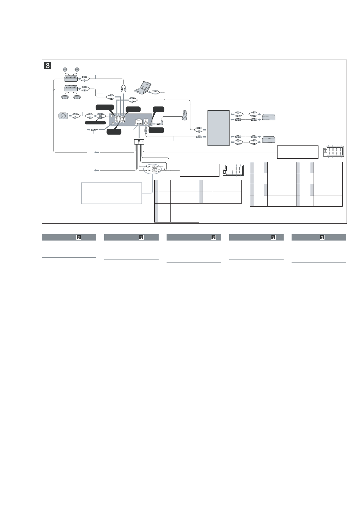
• CDX-GT617UE
A
SUB OUT (MONO)
AUDIO OUT
REAR
AUDIO OUT
FRONT
Connection example
Notes
(2-A)
•
Be sure to connect the ground (earth) lead before connecting
the amplifi er.
•
The alarm will only sound if the built-in amplifi er is used.
(2-B-
Tip
For connecting two or more CD/MD changers, the source
selector XA-C40 (not supplied) is necessary.
)
B
BUS AUDIO IN
BUS CONTROL IN
BUS AUDIO IN
Source selector*
XA-C40
BUS CONTROL IN
*
not supplied
*
8
CDX-GT610U/GT616U/GT617UE
L
R
AUDIO
OUT
REAR
AUDIO
OUT
FRONT
BUS
AUDIO
IN
BUS
CONTROL IN
13 57
24 68
57
48
6
AUDIO OUT
REAR
REMOTE
IN
AUDIO OUT
FRONT
BUS AUDIO IN/
AUX IN
*
3
SUB OUT (MONO)
Negative polarity positions 2, 4, 6, and 8 have striped leads.
1
Purple
+
Speaker, Rear, Right
5
White
+
Speaker, Front, Left
2–
Speaker, Rear, Right
6–
Speaker, Front, Left
3
Grey
+
Speaker, Front, Right
7
Green
+
Speaker, Rear, Left
4–
Speaker, Front, Right
8–
Speaker, Rear, Left
AMP REM
Max. supply current 0.3 A
Fuse (10 A)
Blue/white striped
*
2
Light blue
from the car’s power connector
See “Power connection diagram” on the reverse
side for details.
*
1
Note for the antenna (aerial) connecting
If your car antenna (aerial) is an ISO
(International Organization for Standardization)
type, use the supplied adaptor
2
to connect
it. First connect the car antenna (aerial) to the
supplied adaptor, then connect it to the antenna
(aerial) jack of the master unit.
*
2
RCA pin cord (not supplied)
*
3
Be sure to match the color-coded cord for
audio to the appropriate jacks from the unit. If
you connect an optional CD/MD changer, you
cannot use AUX IN terminal.
*
4
Supplied with the auxiliary equipment
*
5
Insert with the cord upwards
*
6
Supplied with XA-C40
from the car’s speaker
connector
ATT
*
2
Source selector
(not supplied)
XA-C40
*
5
*
2
4
Yellow continuous power supply
7
Red switched power supply
5
Blue power antenna (aerial) control
8
Black ground (earth)
6
Orange/White switched illumination power supply
*
5
*
1
*
2
*
3
*
4
*
5
*
6
*
4
*
6
*
1
from car antenna (aerial)
Auxiliary equipment such as portable DVD
player (not supplied)
2
3
Connection diagram
A To AMP REMOTE IN of an optional power
amplifi er
This connection is only for amplifi ers. Connecting any other
system may damage the unit.
B To the interface cable of a car telephone
Warning
If you have a power antenna (aerial) without a relay box,
connecting this unit with the supplied power supply lead
may damage the antenna (aerial).3
Notes on the control and power supply leads
•
The power antenna (aerial) control lead (blue) supplies +12 V
DC when you turn on the tuner, or when you activate the AF
(Alternative Frequency) or TA (Traffi c Announcement) function.
•
When your car has built-in FM/MW/LW antenna (aerial) in the
rear/side glass, connect the power antenna (aerial) control
lead (blue) or the accessory power input lead (red) to the
power terminal of the existing antenna (aerial) booster. For
details, consult your dealer.
•
A power antenna (aerial) without a relay box cannot be used
with this unit.
Memory hold connection
When the yellow power input lead is connected, power will
always be supplied to the memory circuit even when the ignition
switch is turned off.
Notes on speaker connection
•
Before connecting the speakers, turn the unit off.
•
Use speakers with an impedance of 4 to 8 ohms, and with
adequate power handling capacities to avoid its damage.
•
Do not connect the speaker terminals to the car chassis, or
connect the terminals of the right speakers with those of the
left speaker.
•
Do not connect the ground (earth) lead of this unit to the
negative (–) terminal of the speaker.
•
Do not attempt to connect the speakers in parallel.
•
Connect only passive speakers. Connecting active speakers
(with built-in amplifi ers) to the speaker terminals may damage
the unit.
•
To avoid a malfunction, do not use the built-in speaker leads
installed in your car if the unit shares a common negative (–)
lead for the right and left speakers.
•
Do not connect the unit’s speaker leads to each other.
Note on connection
If speaker and amplifi er are not connected correctly, “FAILURE”
appears in the display. In this case, make sure the speaker and
amplifi er are connected correctly.
9
CDX-GT610U/GT616U/GT617UE
Ver. 1.1
SECTION 2
DISASSEMBLY
Note: This set can be disassemble according to the following sequence.
SET
2-1. SUB PANEL ASSY
(Page 11)
2-2. CD MECHANISM BLOCK
(Page 11)
2-3. MAIN BOARD
(Page 12)
2-4. SERVO BOARD
(Page 12)
2-5. CHASSIS (T) SUB ASSY
(Page 13)
2-6. ROLLER ARM ASSY
(Page 13)
2-7. CHASSIS (OP) ASSY
(Page 14)
1. CHUCKING ARM SUB ASSY
(SUPPLEMENT-1 Page 1)
2. SLED MOTOR ASSY
(SUPPLEMENT-1 Page 2)
3. OPTICAL PICK-UP SECTION
(SUPPLEMENT-1 Page 3)
10
4. OPTICAL PICK-UP
(SUPPLEMENT-1 Page 3)
Note: Follow the disassembly procedure in the numerical order given.
s
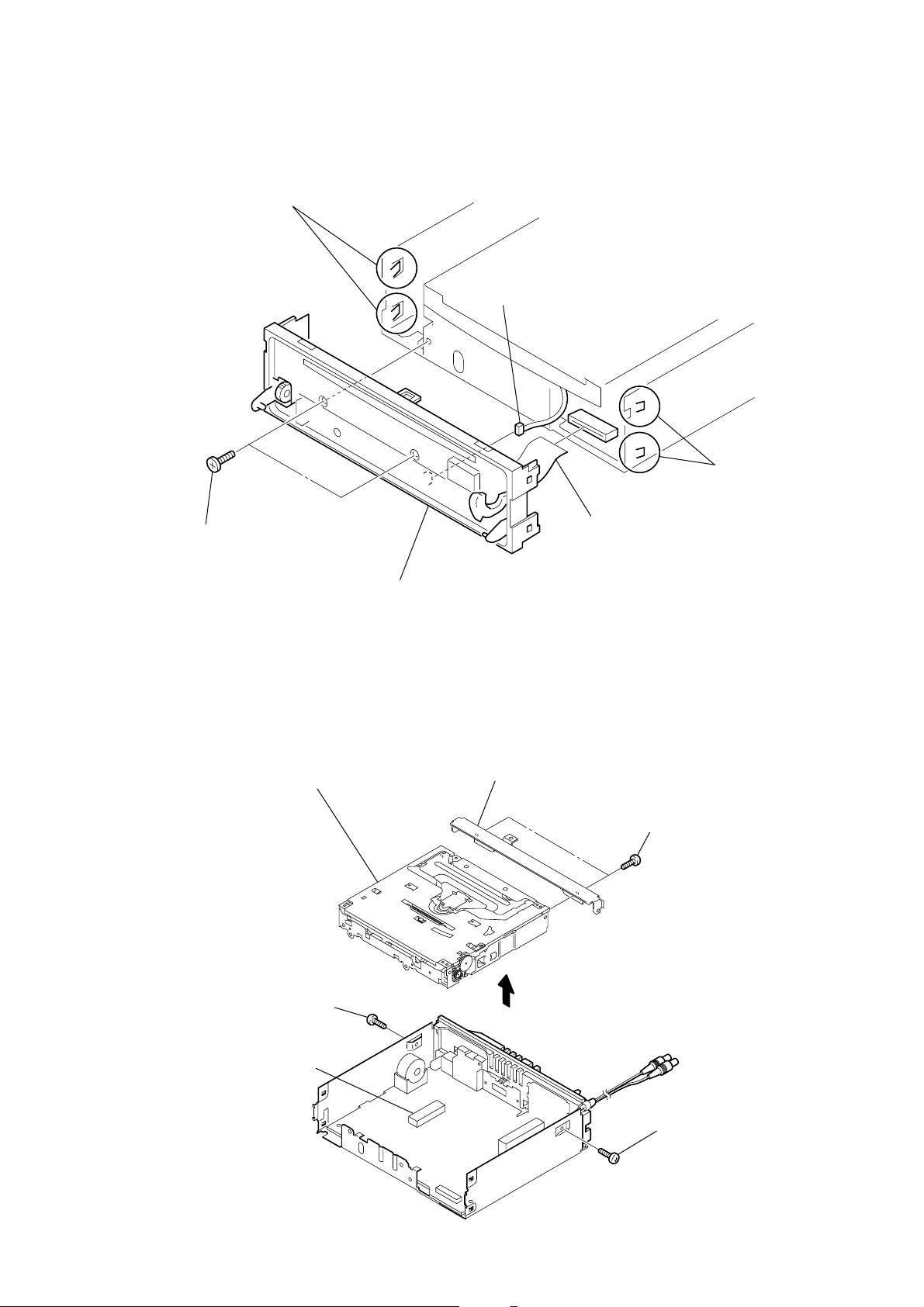
2-1. SUB PANEL ASSY
3
two claws
4
CN203 (3P)
CDX-GT610U/GT616U/GT617UE
2
two claw
1
two
screws
(+PTT 2.6
×
6)
2-2. CD MECHANISM BLOCK
7
2
screw
(+PTT 2.6
×
6
sub panel assy
CD mechanism block
6)
6
bracket (CD)
3
5
flexible flat cable (20 core)
(CN802)
5
two
screws
(+PTT 2.6
×
4)
4
CN350
1
screw
(+PTT 2.6
×
6)
11
CDX-GT610U/GT616U/GT617UE
)
2-3. MAIN BOARD
7
screw
1
three ground point
(+PTT 2.6
×
(+PTT 2.6
screws
6)
×
10)
3
8
two
screws
(+P 2.6
×
9
4
qd
MAIN board
insulating sheet
8)
two
screws
(+PTT 2.6
0
qs
heat sink
CN410 (3P)
×
10)
two
screws
(+P 2.6
qa
5
screw
(+PTT 2.6
×
8)
screw
(+PTT 2.6
×
×
2
two
(+PTT 2.6
10)
8)
screws
×
6
cord (RCA)
8)
2-4. SERVO BOARD
WHT
RED
BLK
WHT
RED
BLK
RED
ORG
BLU
YEL
GRY
1
Remove the eleven solders.
SERVO board
claw
2
toothed lock
(M 1.7
×
2.5)
screw
3
toothed lock
(M 1.7
×
2.5)
5
SERVO board
4
optical pick-up (16 core
(CN1)
claw
screw
12
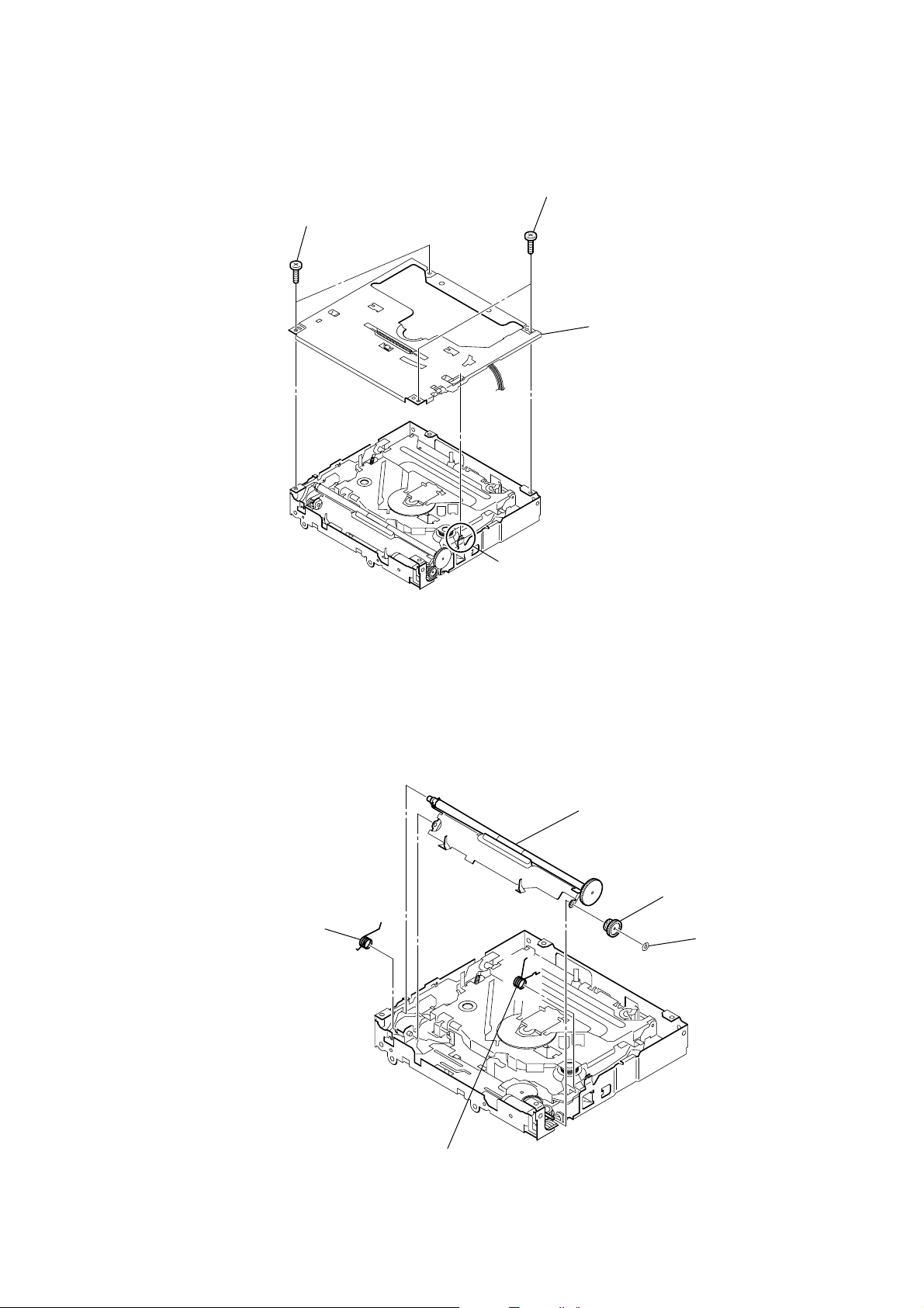
2-5. CHASSIS (T) SUB ASSY
1
two precision
(+P 1.7
×
2.2)
screws
CDX-GT610U/GT616U/GT617UE
2
two precision
(+P 1.7
4
screws
×
2.2)
chassis (T) sub assy
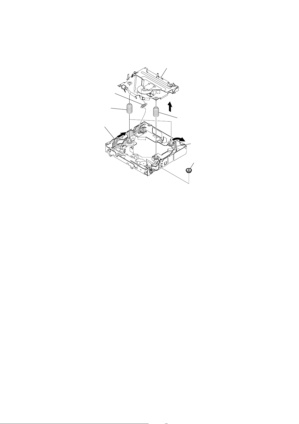
2-6. ROLLER ARM ASSY
1
spring (RAL)
3
claw
5
roller arm assy
4
gear (RA1)
3
washer
2
spring (RAR)
13
CDX-GT610U/GT616U/GT617UE
)
Ver. 1.1
2-7. CHASSIS (OP) ASSY
1
tension spring (KF)
7
coil spring (damper) (natural)
4
slider (R)
6
chassis (OP) assy
5
8
coil spring (damper) (green
3
lever (D)
2
gear (LE1)
14
CDX-GT610U/GT616U/GT617UE
SECTION 3
DIAGNOSIS FUNCTION
Description of the Diagnostics function:
1. Setting the Diag display mode
With the power of f, press the [4] button, [5] button, and [4] button
on the set body or the remote control (for more than 2 seconds)
in turn.
2. Canceling the Diag display mode
During the Diag function mode, press the [OFF] button.
3. Initial display in the Diag display mode.
Just when the Diag mode is entered, “reset count” is displayed.
The display mode is switched by each rotation of
SEEK +/M > or SEEK – /. m keys.
Reset count display
01 XX
Reset count by watchdog timer display
02 XX
Number of connected units display
031 XXX
Operating hours display
04 XXXX
4. Contents of each display mode
4-1. Reset count display mode
01 XX
Reset count
(in hexadecimal format)
Diag code
01: Reset count
4-2. Reset count by watchdog timer display mode
02 XX
Reset count
(in hexadecimal format)
Diag code
02: Number of resets by watchdog timer
4-3. Number of connected units display mode
031 XXX
Show the number of connected units for
CD-C, MD-C and XM respectively from
the rightmost (in hexadecimal format).
Recency of information
1-3: 1 represents the latest.
Diag code
03: Number of connected unit.
The display mode is switched by each rotation of [2/GP/ALBM+] or
[1/GP/ALBM--] keys during the number of connected units display
mode.
CD error information display
051 XX
OFFSET/FAILURE error display
061XXXXX
USB error information display
071 XX
No. of connected units history 1 (latest) display
031 XXX
No. of connected units history 2 display
032 XXX
No. of connected units history 3 display
033 XXX
4-4. Operating hours display mode
04 XXXX
Operating hours
(in hexadecimal format)
Diag code
04: Operating hours
15

CDX-GT610U/GT616U/GT617UE
4-5. CD error information display mode
4-5-1. Error description
051 XX
Error description
(in hexadecimal
format)
Recency of information
1-3: 1 represents the latest.
Diag code
05: CD error information
4-5-2. Disc type and operating hours
Error information
Indication Description
1X SERVO ERROR
3X LOADING ERROR
4X TRACK JUMP
5X TEXT ERROR
FX MECHA ERROR
051 XXXX
Operating hours
Recency of information
1-3: 1 represents the latest.
Diag code
05: CD error information
The display mode is switched by each rotation of [2/GP/ALBM+] or
[1/GP/ALBM--] keys during the CD error information display mode.
Disc type
Indication Disc type
0 MP3
1 WMA
2 AAC
3ATRAC
8 CD/DA
F UNKNOWN
4-6. OFFSET/FAILURE error display mode
061XXXXX
Operating hours
Error description
(0: OFFSET, 1: FAILURE)
Recency of information
1-3: 1 represents the latest.
Diag code
06: OFFSET/FAILURE
The display mode is switched by each rotation of [2/GP/ALBM+] or
[1/GP/ALBM--] keys during the OFFSET/FAILURE error display
mode.
OFFSET/FAILURE error history 1 (latest) display
061XXXXX
OFFSET/FAILURE error history 2 display
062XXXXX
OFFSET/FAILURE error history 3 display
CD error info history 1 (latest)
Error description plus error details display
051 XX
CD error info history 1 (latest)
Disc type plus operating hours display
051 XXXX
CD error info history 2
Error description plus error details display
052 XX
CD error info history 2
Disc type plus operating hours display
052 XXXX
CD error info history 3
Error description plus error details display
063XXXXX
4-7. USB error information display mode
4-7-1. Error description
071 XX
Error description
(in hexadecimal
format)
Recency of information
1-5: 1 represents the latest.
Diag code
07: USB error information
Error information
Indication Description
15 DEVICE ERROR
17
1E
1F BOOT ERROR
3A
43 READ ERROR
44
FA
FB
FILE ERROR
(NO MUSIC)
POWER ON ERROR
INVALID EJECT
ERROR
INVALID
FORMAT FILE
NOT SUPPORT
DEVICE
HUB NOT
SUPPORT
16
053 XX
CD error info history 3
Disc type plus operating hours display
053 XXXX

CDX-GT610U/GT616U/GT617UE
4-7-2. Disc type and operating hours The display mode is switched by each rotation of [2/GP/ALBM+] or
[1/GP/ALBM--] keys during the CD error information display mode.
071 XXXX
Operating hours
Recency of information
1-5: 1 represents the latest.
Diag code
07: USB error information
USB error info history 1 (latest)
Error description plus error details display
071 XX
USB error info history 1 (latest)
Disc type plus operating hours display
071 XXXX
USB error info history 2
Error description plus error details display
072 XX
USB error info history 2
Disc type plus operating hours display
072 XXXX
USB error info history 3
Error description plus error details display
073 XX
USB error info history 3
Disc type plus operating hours display
073 XXXX
USB error info history 4
Error description plus error details display
074 XX
USB error info history 4
Disc type plus operating hours display
074 XXXX
USB error info history 5
Error description plus error details display
075 XX
USB error info history 5
Disc type plus operating hours display
075 XXXX
17

CDX-GT610U/GT616U/GT617UE
MEMO
18

SECTION 4
DIAGRAMS
4-1. BLOCK DIAGRAM — MAIN SECTION —
J451 (1/2)
LL
CDM ON
Z MUTE
WAKE UP
EJECT OK
SYS RST
DR+6V
BU+3.3V
A+3.3V
D+3.3V
TU1
(TUNER UNIT)
L-CH
ANT
R-CH
VCC
VDD+5V
E2PVDD
TU-SCL
TU-SDA
S-METER
TU MUTE
E2P SCL
E2P SDA
QUALITY
MUTE CON
RDS OUT
BUS-RCH
CD L
CD R
A ATT
CD ON
BU IN
RXD
TXD
4
3
10
11
15
13
14
6
7
16
17
5
8
9
SCL
SDA
Q471
JJ
CD-RCH
MUTE CONTROL
SWITCH
Q423
CDON
CDMON
ZMUTE
WAKE UP
EJECT OK
SYSRST
BU IN
MC TX
MC RX
MECHA+6V
BU+3.3V
SERVO+3.3V
K
TU-RCH
AUDIO+8.3V
TUNER+5V
BU+3.3V
X50
8.664MHz
REG
Q3
AUDIO+8.3V
BU+3.3V
REG
IC502
NOISE MASK
SWITCH
RDS MODULATOR
16
MPX
10
XTO
9
XTI
J1
(ANTENNA)
BUS
AUDIO
IN
CD
MECHANISM
UNIT
(MG-101U)
(1/2)
f
K
L
R
1
MUTE
Q426
Q1
IC50
SCL
SDA
INTN
VDDA
VDDD
K
BU+5V
11
12
15
1
7
BUS-RCH
CD-RCH
TU-RCH
SCL
SDA
RDS+3.3V
SWITCH
Q50
ELECTRONIC VOLUME
IC401
9
BUS-LCH
7
BUS-RCH
6
CD-LCH
5
CD-RCH
4
TU-LCH
3
TU-RCH
CDMON
CDON
ZMUTE
WAKE UP
EJECT OK
MC RX
MC TX
BU+3.3V
OUTR2
OUTR1
OUTF2
OUTF1
OUTS2
CLK
DATA
SOUT
MUTE
SCL
SDA
23
24
25
26
21
17
18
19
28
29
30
17
AUX SW
99
CDM ON
98
CDON
93
Z MUTE
91
WAKE UP
89
EJECT OK SW
27
MC RX
28
MC TX
39
VSM
12
TUATT
25
EEP CKO
24
EEP SIO
13
NSMASK
38
QUALITY
53
TU ATTIN
56
DAVN
30
RDS ON
R-CH
(REAR)
R-CH
(FRONT)
SA CLK
SA DATA
SA IN
SCL
SDA
SYSTEM CONTROL
IC501 (1/2)
SA CKO
SA DATA
I2C CKO
I2C SIO
VOLATT
AMPSTB
ACCIN
ILLUIN
TELATT
TESTIN
BUSON
UNISCK
UNISO
SYSRST
KK
KK
KK
MUTE
MUTE
SA IN
ATT
BEEP
DIAG
BUIN
UNISI
MUTE
Q470
MUTE CONTROL
SWITCH
Q491,492
45
44
32
33
34
9
86
7
26
8
72
75
74
73
87
60
54
58
59
88
SA CLK
SA IN
SA DATA
SCL
SDA
BUIN
ILLUMINATION CHECK
D400
SYSRST
Q703
Q440
12
11
10
8
9
13
RESET
Q430
D491
BUS INTERFACE
BUS IN
CLK IN
B/U-C
DATA OUT
DATA IN
RST
A
I2C BUS CONTROLLED POWER AMP/
K
MULTIPLE VOLTAGE REGULATOR
11
K
BATT
IC601
DISPLAY
SECTION
SDA
SCL
DATA I/O
BUS ON
IN RF
12
IN RR
2
SDA
4
SCL
16
BEEP
22
STB
25
DIAG
ACCESSORY CHECK
TELEPHONE ATTENATION CHECK
BATT
3
4
CLK
6
1
2
RST
(Page 20)
IC300
AMP REM
Q702
Q701
OVER VOLTAGE
OUT FL+
OUT FL–
OUT RL+
OUT RL–
ANT REM
VP1
VP2
REG1
REG2
REG3
REG4
REG5
CHECK
Q605
CDX-GT610U/GT616U/GT617UE
J451 (2/2)
CN410
CN300
7
4
5
6
8
: CD PLAY
: FM
: MW/LW
: BUS
1
9
2
10
4
12
3
11
5
6
16
7
14
13
15
TH400
L
R
L
R
FL+
FL–
RL+
RL–
FR+
FR–
RR+
RR–
AMP-REM
ANT-REM
BATT
ACC
ILL
TEL ATT
TEST
1
2
3
AUDIO OUT
REAR
AUDIO OUT
FRONT
L
R
BATT
CNJ400
BUS
CONTROL IN
SUB
OUT
K
R-CH
(REAR)
K
R-CH
(FRONT)
K
5
3
9
7
29
27
BATT
VP
35
20
6
30
AUDIO+8.3V
37
BU+5V
31
SERVO+3.3V
33
MECHA+6V
34
PANEL+B
D602
K
K
K
K
R-CH
FU601
BATT
• R-CH is omitted due to same as L-CH.
• Signal Path
J
K
f
L
CDX-GT610U/GT616U/GT617UE
19 19

CDX-GT610U/GT616U/GT617UE
4-2. BLOCK DIAGRAM — DISPLAY SECTION —
KEY MATRIX
S201,902–904,906–917
(Page 19)
LSW901,
RE901
PUSH SELECT
(VOLUME)
ROTARY
ENCODER
J370
(REMOTE IN)
PANEL+B
MAIN
SECTION
BU+3.3V
FL900
SYSTEM CONTROL
IC501 (2/2)
KEYIN0
41
FL SO
KEYIN1
40
D501
KEY ACKNOWLEDGE
SWITCH
Q501
S102
(NOSE DET)
REMOTE CONTROL
SIGNAL RECEIVER
IC971
RESET
A
RESET
IC602
52
76
47
48
71
43
5
64
77
KEYACK
AD ON
RE-IN0
RE-IN1
RC IN1
RC IN0
NOSE SW
SIRCS
RESET
FL SCK
FL CS
XIN
XOUT
OSCOUT
OSCIN
FL12V ON
DD ON
FSW OUT
19
20
18
80
79
83
82
65
67
66
X501
32.768kHz
X500
18.432MHz
SHIFT
CONTROL
SWITCH
BATT
Q801
FLUORESCENT
INDICATOR TUBE
12
DIO
CLK
11
CS
10
DC-DC CONVERTER
IC802
1
VIN
SW
EN
7
6
RT
INV
FB
GRID1
GRID2
GRID3
RESET
VDD(3.3V)
2
5
3
3G
2G
1G
Q1
Q2
VH
F+
F–
28
27
26
35
34
33
32
31
13
7
PANEL+3.3V
8
39
•
38
2
•
1
FL DRIVE
Q991
FL VH+12V
D982
FL DRIVE
Q992
PANEL+3.3V
PANEL+3.3V
D802
REG
IC804
FL DRIVE
Q993
FL +12V
IC801
USB CONTROL
IC803
2
•
IN
3
EN
4
OC
5
LED DRIVE
REG
OUT
FL VH+12V
Q941
6
•
7
•
8
LED902–904,
906–917,
941–944,
LSW901
BATT
LED DRIVE
V–BUS
Q942
LED952–954,
956–967,
991–994,
LSW901
PANEL+B
CDX-GT610U/GT616U/GT617UE
LED202
Z
DOOR INDICATOR
CONTROL SWITCH
LED201
CD
INDICATOR
Q589,590
S103
RESET
BU+5V
46
DOOR IND
FSW IN
USB ON
USB OVER
DOOR SW
10
22
21
70
D997
D998
S918
OPEN/
CLOSE
Q503
V-BUS
CD
MECHANISM
UNIT
(MG-101U)
(2/2)
USB D+
USB D–
USB SELECT SWITCH
IC980
2C
3
1C
7
1B
2
2A
5
2B
1A
J11
5
6
1
J11
4
3
2
1
2020

CDX-GT610U/GT616U/GT617UE
• NOTE FOR PRINTED WIRING BOARDS AND SCHEMATIC DIAGRAMS
THIS NOTE IS COMMON FOR PRINTED WIRING
BOARDS AND SCHEMATIC DIAGRAMS.
(In addition to this, the necessary note is
printed in each block.)
For schematic diagrams.
Note:
• All capacitors are in µF unless otherwise noted. (p: pF)
50 WV or less are not indicated except for electrolytics
and tantalums.
• All resistors are in Ω and 1/
specified.
• f : internal component.
• C : panel designation.
Note: The components identified by mark 0 or dotted line
with mark 0 are critical for safety.
Replace only with part number specified.
• A : B+ Line.
• B : B– Line.
• H : adjustment for repair .
•Voltages and waveforms are dc with respect to ground
under no-signal (detuned) conditions.
no mark : FM
(): MW/LW
<>: CD PLAY
•Voltages are taken with a VOM (Input impedance 10 MΩ).
Voltage variations may be noted due to normal production
tolerances.
•Waveforms are taken with a oscilloscope.
Voltage variations may be noted due to normal production
tolerances.
• Circled numbers refer to waveforms.
• Signal path.
J : CD PLA Y
F : FM
f : MW/LW
L : BUS
: Impossible to measure
∗
4
W or less unless otherwise
For printed wiring boards.
Note:
• X : parts extracted from the component side.
• Y : parts extracted from the conductor side.
a
•
• : Pattern from the side which enables seeing.
(The other layers' patterns are not indicated.)
Caution:
Pattern face side: Parts on the pattern face side seen from the
(Side B) pattern face are indicated.
Parts face side: Parts on the parts face side seen from the
(Side A) parts face are indicated.
: Through hole.
C
Q
These are omitted
EB
E
CB
These are omitted
C
BE
These are omitted
• Waveforms
— MAIN Board —
1
IC501 i; (XIN)
32.768 kHz
0.2 V/DIV, 20 µsec/DIV
2
IC501 is (OSC IN)
18.432 MHz
0.5 V/DIV, 0.1
3
IC50 9 (XTI)
0.5 V/DIV, 0.1
µ
sec/DIV
8.664 MHz
µ
0.7 Vp-p
0.9 Vp-p
1.1 Vp-p
sec/DIV
CDX-GT610U/GT616U/GT617UE
21 21

CDX-GT610U/GT616U/GT617UE
4-3. PRINTED WIRING BOARD — MAIN SECTION —
234567891011 12 13 14
J451
AUDIO OUT
REAR
LR
C432
R432
R417
Q430
JC490
JC491
C443
JW25
JW65
JC493
R454
D107
C480
C481
R453
R455
R557
D106
C454
JW44
R421
JC304
R431
C431
C441
C327
C328
R480
C482
C483
R484
D118
C104
D105
JW155
C806
D104
Q440
JW22
C421
JC305
R521
JW151
C452
R452
C487
JW143
C446
C447
R441
C471
C461
C485
C484
IC401
JW62
JW63
JW64
JC522
JW108
JW142
R558
D119
C814
D120
D103
C3
JC3
C9
C58
Q589
CN410
R9
R7
IC50
C56
Q590
BUS
AUDIO IN
LR
-1 -2 -3 -4
R474
C470
C414
Q471
R416
JW24
C14
R411
C411
C361
C360
JW45
C1
R5
R1
JW66
Q1
C2
D2
R10
C7
C5
L1
L4
JC32
JW113
JW114
L2
R11
JC9
L3
X50
C57
D102
C108
JW158
D110
D109
D108
R542
C109
C110
D114
C62
D101
JW23
(CHASSIS)
JC494
C362
R483
R482
Q3
JW148
JW152
C114
D471
C413
R418
R419
JW26
JC492
R481
JW110
JW111
JW112
JW160
JW147
R813
CN802
D115
A
B
C
D
E
F
G
H
J
1
J1
(ANTENNA)
JC998
TU1
(TUNER UNIT)
R2
R3
R4
R8
JW115
R55
C61
C50
C51
Q50
R14
C52
C53
R54
R57
JW149
R12
R13
C8
R6
JW67
JW68
R554
JW81
R58
C54
C55
R53
R52
C60
I
JW153
JW154
L101
(CHASSIS)
: Uses unleaded solder.
AUDIO OUT
FRONT
LRLR
-5 -6
JC999
C442
C422
R422
R442
Q420
C472
JW21
C423
C465
C303
Q460
Q470
JW27
R471
R461
R440
R420
R470
R460
R450
R433
C364
JW109
JW107
R549
R548
JC503
JC501
R520
JW140
JW141
C803
JC806
JW150
C103
C466
C363
R518
IC804
JW80
JW105
R517
JC508
JW139
(SUB OU
12 3
JW17
JW18
JW19
JW20
C308
C306
JW40
JW41
JC400
JW58
JW59
JW60
JW61
JW104
R509
R500
R540
R519
C513
JW138
CN410
JC515
JW137
C317
JW103
JW4
C320
R514
R539
C510
JW135
T)
C309
C310
JC506
JC514
JW136
C491
Q491
JW102
R515
C523
C511
JW133
JC302
IC300
C312
JW43
R301
C319
R545
JC516
R516
R513
JW101
JW134
IC803
C504
C509
C508
JW132
C307
Q492
JC518
JW100
JC523
C512
JC300
JW38
JW39
C318
R572
R573
JW156
JW131
C462
D491
R302
C507
JW130
R535
C305
JW37
R491
JW99
JC301
JC504
JW129
D305
JW36
JW98
JW16
R510
JW57
JW78
JW79
JW128
D501
Q426
R371
JW15
D306
JW35
IC502
JW56
GT61OU
/GT616U
R571
R555
D502
C324
C304
JW14
D307
FMB4
C503
R505
GT617UE
R559
R556
R811
JW2
JW13
C325
Q424
FMB3
JW34
R504
JC512
R523
JW127
C323
D308
C314
GT617UE
IC501
R525
JC511
R524
R810
JW157
R506
R503
R502
R512
Q501
D802
R812
D310
C501
+B 14.4V
C301
JW3
JW12
D311
C313
JC429
JC495
R541
R526
JC90
JW11
JW33
C316
C315
C502
JW54
JW55
GT61OU
/GT616U
X501
FB804
C804
D312
JW125
JW10
JW53
R425
R570
C506
R522
X500
R424
Q423
YEL
D309
R547
JW124
C816
JW9
C429
C430
JW76
C515
R529
JW123
IC801
C817
FB402
R423
R536
R530
1
2
354
JW75
R537
C516
JW8
R703
R702
JW52
FB401
C403
C410
C418
C419
R401
JC350
JW77
C505
X500
R370 R546
R528
JW121
JW122
D302
C412
R402
FB403
GT617UE
R563
L500
JW119
JW120
S103
S103
RESET
D301
R561
JW74
GT61OU
/GT616U
R551
JW97
JW118
JC524
JC804
C805
R704
R562
JW96
JC53
Q701
CN350
D400
JC510
R543
R701
JW94
JW95
D701
JW117
CN300
FU601
JW92
IC602
D703
R574
R553
R527
C519
R808
JW1
C402
Q703
C998
C821
JW7
C901
C902
JW90
R531
D903
R709
C417
FB407
FB406
FB405
C415
FB404
R351
C703
JW89
R532
FB801
R806
L803
D304
D303
JW29
JW30
JW31
JW32
C401
R711
JW88
R533
JC519
C405
C812
JW46
JW49
L802
C830
CNJ400
(BUS CONTROL IN)
CNJ400
87
321
654
D605
D606
C701
FB408
JW51
JW72
JW73
R712
D705
JW87
JW86
R534
C601
R830
FB803
S102
S102
(NOSE DET)
D704
JC600
R602
R802
C704
JW85
R601
R809
FB802
R801
C705
JW50
R710
R708
D801
R803
D607
JW69
R707
Q801
YEL
+B 14.4V
R705
IC601
C802
R804
R706
D702
C702
C810
JC997
C602
JW5
TH400
JW47
Q605
JW6
Q702
R805
D604
C819
R606
R607
R605
1
7
C811
D602
JW84
JW83
C809
C600
JC603
R603
D603
JC602
JW82
IC802
J370
(REMOTE IN)
L301
L302
L303
L300
JW28
R611
R610
R604
L801
R600
1-872-074-
C801
C822
BATT
• Semiconductor Location
Ref. No. Location Ref. No. Location
D2 F-2
D101 I-2
CD
MECHANISM
UNIT
(MG-101U)
(1/2)
CN2
D102 I-2
D103 J-3
D104 J-3
D105 J-3
D106 J-3
D107 J-3
D108 J-2
D109 J-2
D110 I-2
D114 J-2
D115 J-2
D118 I-3
D119 I-4
D120 J-4
D301 D-8
D302 D-8
D303 D-9
D304 C-9
D305 D-6
D306 C-6
D307 C-6
D308 D-6
D309 D-7
D310 D-6
D311 D-7
D312 D-7
D400 H-8
D471 B-3
D491 E-5
D501 I-6
D502 I-6
D602 F-10
D603 F-10
D604 F-10
11
D605 B-10
D606 C-10
D607 C-10
D701 C-8
D702 G-10
D703 D-8
D704 F-9
D705 G-9
D801 I-10
D802 I-6
D903 C-9
IC50 H-2
IC300 B-5
IC401 E-3
IC501 H-6
IC502 E-6
IC601 H-10
IC602 I-8
IC801 I-7
IC802 I-10
IC803 J-5
IC804 I-4
Q1 E-2
Q3 F-2
Q50 H-1
Q420 C-4
Q423 F-7
Q424 E-6
Q426 E-6
Q430 C-3
Q440 C-3
Q460 C-4
Q470 C-4
Q471 B-2
Q491 E-5
Q492 E-5
Q501 I-6
Q589 I-2
Q590 I-2
Q605 F-10
Q701 D-8
Q702 G-10
Q703 G-9
Q801 I-10
SUB BOARD CN202
CDX-GT610U/GT616U/GT617UE
(Page 26)
2222

CDX-GT610U/GT616U/GT617UE
4-4. SCHEMATIC DIAGRAM — MAIN SECTION (1/3) —
CN300
FU601
R701
R710
R705
R709
L300
D701
D702
D607
D703
C704
C701
• Refer to page 30 for IC Block Diagrams.
R702
C705
R703
D705
D704
R706 R708
C703
D903
R704
R711
R712
R707
C702
C901C902
Q701
Q703
Q702
JC504
IC300
R302
C319
R301
C318
C317
C303
JC302
C323
JC301JC300
C301
C472 C462
R491 D491
C465C466
JC495
C491
C324
C304
D305D306D307D308D309D310D311D312
Q491
Q492
JW43
C325 C502
D302
D301
D303 D304
IC502
C306
C305
C501
C316
C308
C315
C307
C314
C313
C312
C309
C310
JC999
(Page 24)
C320
CDX-GT610U/GT616U/GT617UE
J370
CNJ400
C602
L303
L302
L301
JC603
TH400
C600
R611
R610
D606
R600
R606
R604 R603
D603 D602
JC602
R607
D605D604
R605
IC601
Q605
C601
R601R602
JC510
IC B/D
(Page 25)
23 23

CDX-GT610U/GT616U/GT617UE
4-5. SCHEMATIC DIAGRAM — MAIN SECTION (2/3) —
CN410
C443 C447
C423 C446
R471
C471
C411
R411
JW25
JW26
Q460Q470
JC491 JC305
R461
C461
C442 C422
Q440
Q420 Q430
JC490
R441 R421 R431
C441
C421
• Refer to page 21 for Waveforms.
• Refer to page 30 for IC Block Diagrams.
J451
C452 C432
R452R422R442
JC304
R432
C431
C413 C414
R418 R416
R419 R417
R474
C470
D471
C14
Q471
JC998
J1
TU1
JC32
C8
R6
R13R12
R7
L1
JC3
R8
R9
JW142
C3
R5
R4
C1
Q1
R1
R2
R3
C9
C2
C5
Q3
D2
R10
C7
L4
(Page 23)
JC522
C485
C484
C454
R450
R460
R470
R420
R440
R484
R433
R455
JC400
C487
R454
R453
IC401
IC B/D
C481
R482
R480
C480
C360
C362
C361
C364
C363
C328
C327
C483
C482
JC492
JC493
JC494
R483
R481
Q590
Q589
JW149
R57
JW125 JW158
R542
IC B/D
C50
R55
Q50
R58
C51
C52
C61
C53
C60
R54
R53
R52
C54
IC50
C55
JW151
D118
C58
L2 L3
JC9
R14 C62
R11
C56
X50
JC806
C57
CN802
(Page 27)
CDX-GT610U/GT616U/GT617UE
(Page 25)
L101
C110
2424
D110
C109
D109
C108
D108
C114
D114
D115
D107
D106
D105
D101
C104
D104
D119
C103
D103
5120
D102

4-6. SCHEMATIC DIAGRAM — MAIN SECTION (3/3) —
CDX-GT610U/GT616U/GT617UE
• Refer to page 21 for Waveforms.
• Refer to page 30 for IC Block Diagrams.
• Refer to page 31 for IC Pin Description of IC501.
L801
JC350
FB408
R351
FB407
FB406
FB405
FB404
C405
JW49
C417
C415
CN350
R570
FB401C412 JC429
C403
R402
FB403
C419
R401
C418
FB402
C401
C402
(Page 23)
C410
R423
C429
C430
Q423
Q424
Q426
R424
R425
C505
C506
C515
C516
X500
R536
L500 R537
JC600
R553
R563
R561
D400
X501
R551
R534
R533
R532
R531
R546
R530
R529
R547
R370
S103
IC501
D502
R543
JC53
R528
JC524
R527
C519
R541
JC90
R526
R525
IC602
D501
JC512
C513
C511
C509
C507
R524
R523
R521
C512
C510
C508
R540
R555
R522
Q501
R535
R371
R539
R556
R520
R519
R558
R557
JC508
JC501
(Page 24)
JC511
R830
C830
L802 L803
D801
C802
C822
C801
C809 C810 C821 C811
JC997
C998
IC802
C812
R803
R806
R802
R801
C819
C805
FB801
IC B/D
R808
R805
JC804
R804
FB803
Q801
R809
FB802
R811
D802
JW129 JW128
R810
IC803
JW136
C806
FB804
R813
C816
IC804
C803
C804
C817
IC801
C814
R812
R562
S102
JC519
R500
R503
R505
R502
R504
R506
R559
R509
R512
JC518
R510
R554
JC506
R545
C523
JC523
R571
JC514
R514
R515
JC515
JC516
R516
R573
JW99
JW98
R572
R513
R548 R549
JW78
JW79
C503
C504
R574
JC503
R518R517
CDX-GT610U/GT616U/GT617UE
25 25

CDX-GT610U/GT616U/GT617UE
4-7. PRINTED WIRING BOARD — SUB SECTION —
1
23456789101112
A
B
R201
LED201
C
LED201
(CD INDICATOR)
D
: Uses unleaded solder.
FMA4
LED202
R202
CN201
S201
LED202,S201
Z
E
F
G
H
CD
MECHANISM
UNIT
(MG-101U)
(2/2)
CN101
FMA3
R205
CN203
11
1-872-098-
(11)
B
(Page 22)
MAIN BOARD CN802
KEY BOARD CN901
(Page 28)
A
CN202
3
1
120
R203
R204
D204
D203
I
J
CDX-GT610U/GT616U/GT617UE
C202
11
1-872-098-
(11)
2626

4-8. SCHEMATIC DIAGRAM — SUB SECTION —
CDX-GT610U/GT616U/GT617UE
Ver. 1.1
(Page 24)
CN202
S201
C202
R201 R202
LED201
1
*
LED201,202
1
*
SML-310VTT86
SML-310PTT86
(GT610U/GT616U)
(GT617UE)
LED202
1
*
R205
D204 D203
CN201
(Page 29)
CN203
R204
R203
CDX-GT610U/GT616U/GT617UE
27 27
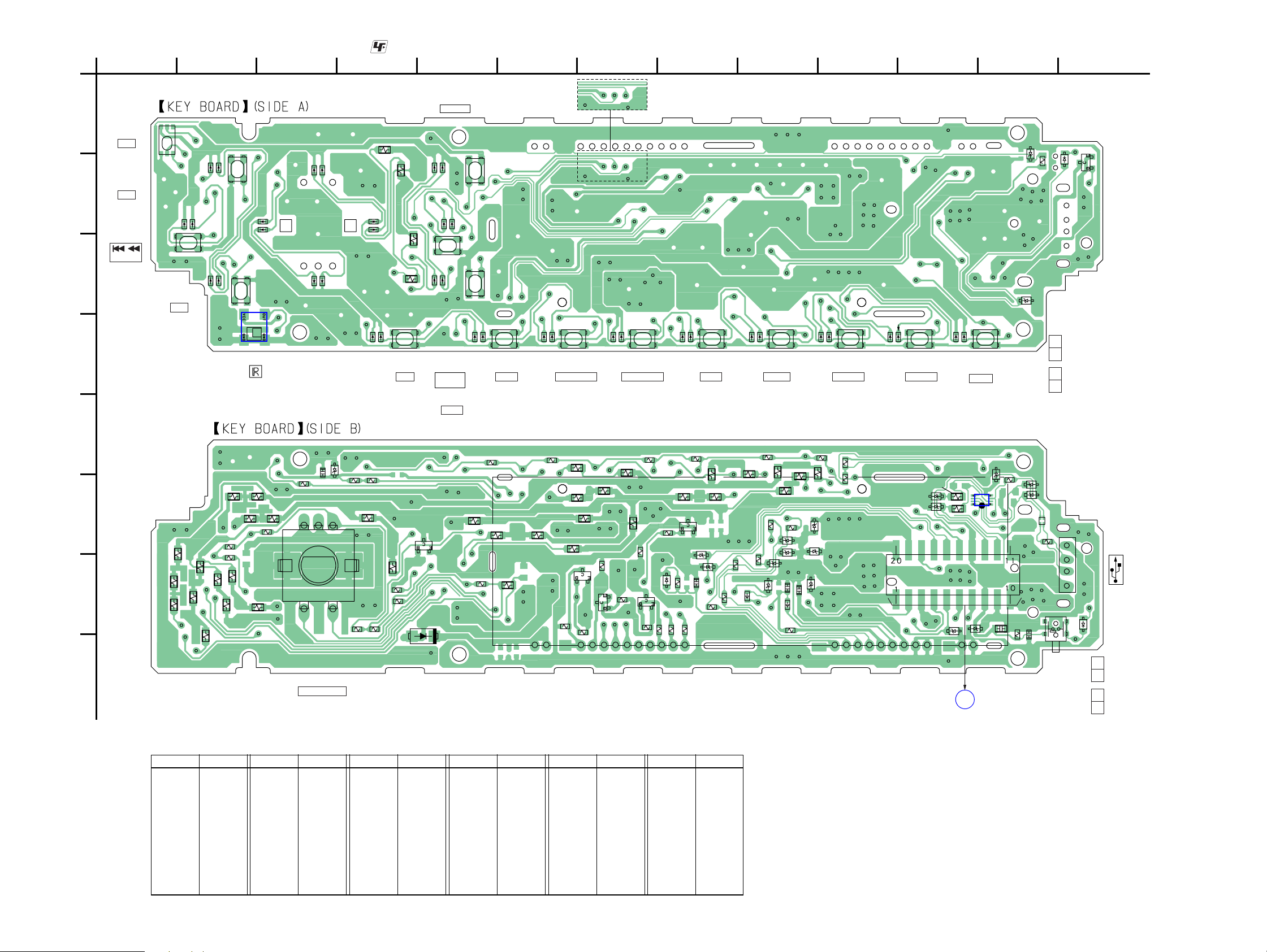
CDX-GT610U/GT616U/GT617UE
Ver. 1.1
4-9. PRINTED WIRING BOARD — KEY SECTION —
: Uses unleaded solder.
A
B
C
D
1
LSW901
OFF
LED908,958,
S908
DSO
LED907,957,
S907
SEEK–
LSW901
S907
LED906,956,
S906
EQ3
2345678910111213
GT617UE
LED964
S914
LED914,964,
S914
2/GP/ALBM+
LED963
LED913
S913
LED913,963,
S913
3/REP
LED912
LED962
S912
LED912,962,
S912
4/SHUF
LED911
LED961
S911
LED911,961,
S911
5/BBE M
D996
D997
R959
D904
LED960
S910
LED910
LED910,960,
P
S910
6/PAUSE
LED909
LED959
S909
LED909,959,
S909
AF/TA
1-872-099-
11
(GT610U/GT616U)
(11)
21
(GT617UE)
(21)
Q503
LED907
LED957
LED958
LED908
LED956
LED906
S908
LED944
LED994
S906
12
43
IC971
LED943
IC971
LED941-944,991-994
(RING ILLUMINATION)
LED991
LED941
LED993
R939
LED992
LED942
R941
LED917
LED967
LED917,967,
R940
S917
S917
PTY
R942
LED902,952,
S902
SOURCE
LED952
LED902
LED953
LED903
S903
LED904
LED954
LED903,953,
S903
M >
SEEK+
LED904,954,
S904
MODE
S902
S904
LED916
LED966
S916
LED916,966,
DSPL
S916
LED965
LED915
S915
LED915,965,
S915
1/GP/ALBM–
GT610U/GT616U
LED914
E
F
G
H
R946
R906
R949
R947
R938
R936
R934
R935
R937
R933
R944
R943
R907
R908
R950
R948
• Semiconductor Location
Ref. No. Location
D902 G-11
D903 E-12
D904 C-12
D931 G-8
D971 E-3
D973 F-11
D976 F-11
D978 F-12
D979 F-12
D981 F-9
D982 D-5
D983 G-9
Ref. No. Location
D984 F-9
D985 F-8
D986 G-8
D989 G-9
D990 G-9
D991 F-9
D992 F-9
D993 G-11
D996 A-12
D997 B-13
D998 G-13
R945
C971
R972
3
5
RE901
2
RE901
PUSH SELECT
(VOLUME)
D971
R973
R971
R957
4
1
R905
R904
Q941
R955
R962
R903
D982
R956
R902
Ref. No. Location Ref. No. Location
IC971 D-3
IC980 F-12
LED912 D-9
LED913 D-8
LED914 D-7
LED902 B-5
LED903 B-5
LED904 C-5
LED906 C-2
LED907 B-2
LED908 B-2
LED909 D-11
LED910 D-10
LED911 D-10
LED915 D-6
LED916 D-5
LED917 D-4
LED941 B-3
LED942 B-4
LED943 C-3
LED944 B-3
LED952 B-5
LED953 B-5
R916
R952
R901
R914
R924
R953
R963
R996
R995
D931
Q993
R992
R988
R993
FLUORESCENT INDICATOR YUBE
39
R954
R915
R994
R922
R921
Q991
R991
R923
R958
R951
Q992
Ref. No. Location Ref. No. Location
LED954 C-5
LED956 C-2
LED957 B-2
LED958 B-2
LED959 D-11
LED967 D-4
LED991 B-3
LED992 B-4
LED993 C-3
LED994 B-3
LED960 D-11
LED961 D-10
LED962 D-9
LED963 D-8
LED964 D-7
LED965 D-6
LED966 D-5
Q503 B-13
Q941 F-5
Q942 F-8
Q991 G-7
Q992 G-7
Q993 G-7
R927
R989
Q942
R966
FL900
R913
D985
R990
D986
C932
R984
R925
R928
R985
R986
R926
R983
FB971
R912
R931
R982
D991
D989
R932
D992
FB991
R981
D990
R987
R929
C991
D984
C992
R911
D981
D983
R930
R910
R909
R964
D976
D973
CN901
SUB BOARD CN201
5
8
R965
D993
B
(Page 26)
IC980
D902
1
D903
4
1
C921
R967
D979
R969
D978
R968
J11
S918
C920
(OPEN/CLOSE)
LF990
5
4
3
2
S918
1-872-099-
J11
D998
11
(GT610U/GT616U)
(11)
21
(GT617UE)
(21)
CDX-GT610U/GT616U/GT617UE
2828

4-10. SCHEMATIC DIAGRAM — KEY SECTION —
CDX-GT610U/GT616U/GT617UE
Ver. 1.1
CN901
LED917
LED916
LED915
D983
D981
R921 R922
R923 R924
LED967
LED914
LED966
LED913
LED965
LED912
D984
R925 R926
R927 R928
LED909
LED964
LED910
LED963
LED911
LED962
R929 R930
R931 R932
LED959
LED941
LED960
LED942
LED961
R939 R940
R941 R942
LED943
LED991
LED944
LED992
R947
R949
R948
R950
LED993
LED902
LED994
LED904
R955 R956
R957 R958
LSW901(2/2)
LED952
LED954
R933 R934
R935 R936
R937 R938
LED908
LED906
R943 R944
R945 R946
LED958
LED956
Q941Q942
LED907
LED903
R951
R953
R952
R954
LED957
D971
LED953
R962
R963
C971
R973
R971
IC971
D931
C932
R972
R966
Q991
R994
Q992
GT610U/GT616U
R992R991
R995
R996
Q993
C991 C992
R993
R989
R984
R985
R986
R987
FB991
GT617UE
R988
R990
D982
FL900
(Page 27)
R983
D973 D976
C920
R981
R982
J11
C921
D902D903
R968
FB971
R964
R965
LF990
D985
D989
D978 D979
D986
D993D996
D904
D990
D992D991
IC980
R901
R959
R969
S902LSW901(1/2)
S909
Q503
D998
R967
R903R902
S903
R910R909 R916
D997
S918
R904
R911
S904
R905
RE901
S906
R913R912
R914
R915
R907R906
S907
S917S916S915S914S913S912S911S910
R908
S908
CDX-GT610U/GT616U/GT617UE
29 29

CDX-GT610U/GT616U/GT617UE
1 2 3 4 5
CURRENT
LIMIT
PWM
COMPARATOR
ERROR
AMP
L:OFF
H:ON
VREF
VIN
TSD
OSC
VIN SW PB GND INV
6
RT7EN
VREF
SOFT
START
ON/OFF
LATCH
DRIVER
RESET
• IC BLOCK DIAGRAMS
IC601 BA8271F-E2 (MAIN Board (1/3))
BUS ON
1
2
RST
BATT
3
4
CLK
5
VREF
6
DATA
GND
7 8
BUS ON
SWITCH
RESET
SWITCH
BATTERY
SWITCH
IC401 BD3442FS-E2 (MAIN Board (2/3))
14
13
12
11
10
9
VCC
RESET
BUS ON
CLK IN
BU IN
DATA IN
DATA OUT
IC50 TDA7333013TR (MAIN Board (2/3))
INTERPOLATOR
1
VDDA
REF3
REF2
REF1
VSS
VDDD
RESETN
2
3
4
5
6
TM
7
8
INTN
MPX
RDS
DEMODULATOR &
SYNCHRONIZATION
RDSREG
BAND PASS
FILTER
RAM
BUFFER
&
CONTROL
LOGIC
3
SDAOUT
SDAIN
SCK
SPI
TESTREG
SIGMA DELTA
CONVERTER
TEST LOGIC
&
PIN MUX'S
OSCILLATOR
16
MPX
15
INTN
14
CSN
13
SA_DATAOUT
12
SDA_DATAIN
11
SCL_CLK
10
XTO
9
XTI
2
SINC4
FILTER
SINC4REG
I2C/SPI
INTERFACE
BUS-RCH
BUS-LCH
TU-RCH
TU-LCH
CD-RCH
CD-LCH
AUX-RCH
AUX-GND
AUX-LCH
DS3-L
DS1-L
DS2-L
EBIAS
DS2-R
DS1-R
DS3-R
10
11
12
13
14
15
16
1
2
3
4
5
6
7
8
9
100k
100k
100k
100k
100k
100k
250k
250k
250k
INPUT
SELECTOR
INPUT
GAIN
SPECTRUM
ANALYZER
VOLUME1
/MUTE
TREBLE
/BASS
/MIDDLE
LPF
EFFECT
FADER
FADER
VOLUME2
FADER
FADER
FADER
FADER
I2C
BUS
LOGIC
VCC2
32
31
30
29
28
27
26
25
24
23
22
21
20
19
18
17
F2L
GND
IC802 BD9778HFP (MAIN Board (3/3))
SDA
SCL
MUTE
VCCVCC
OUT-FR
OUT-FL
OUT-RR
OUT-RL
SUBOUT-R
SUBOUT-L
ADJ
SAOUT
SADA
SACLK
CDX-GT610U/GT616U/GT617UE
3030

CDX-GT610U/GT616U/GT617UE
• IC PIN DESCRIPTION
IC501 MB90F046PF-G-102E1 (SYSTEM CONTROL) (CDX-GT610U/GT616U) (MAIN BOARD (3/3))
IC501 MB90F046PF-G-104E1 (SYSTEM CONTROL) (CDX-GT617UE) (MAIN BOARD (3/3))
Pin No. Pin Name I/O Pin Description
1 AREASEL0 I Destination setting pin 0
2 AREASEL1 I Destination setting pin 1
3 AREASEL2 I Destination setting pin 2
4B-OUTSEL I Black-out with/without discrimination signal input “H”: Black-out
5 NOSE SW I Front panel attachment detect signal input “L”: with panel
6 AAC SEL I AAC play setting signal input “H”: AAC
7 BEEP O Beep signal output to power amplifier
8 DIAG I Status signal input from power amplifier
9 VOLATT O Electronic volume attenuate control signal output
10 FSW IN I D/D converter oscillator frequency count signal input
11 VSS — Ground pin
12 TUATT O Tuner mute control signal output
13 NSMASK O Noise mask signal output
14 NCO O Not used. (Open)
15 ILLUMI SEL I Illumination voltage setting signal input
16 NCO O Not used. (Open)
17 AUX SW O AUX change over signal output “L”: AUX, “H”: BUS IN
18 FL CS O Fluorescent indicator tube chip select signal output
19 FL SO O Fluorescent indicator tube serial data signal output
20 FL SCK O Fluorescent indicator tube serial clock signal output
21 USB OVR I Overcurrent detect signal input from USB power supply high side switch
22 USB ON O USB power supply high side switch control signal output
23 VCC5 — Power supply pin (+3.3 V)
24 EEP SIO I/O EEPROM bus serial data signal input/output
25 EEP CKO O EEPROM bus serial clock signal output
26 AMPSTB O Standby signal output to power amplifier
27 MC RX I Mechanism microcomputer comunication signal input RX
28 MC TX O Mechanism microcomputer comunication signal output TX
29 NCO O Not used. (Open)
30 RDS ON O RDS (Radio Data System) on signal output Tuner on: “L”
31 NCO O Not used. (Open)
32 SA DATA O Data signal output for electronic volume IC spectrum analyzer
33 I2C SCK O I2C bus serial clock signal output
34 I2C SIO I/O I2C bus serial data signal input/output
35 DAVDD — A/D converter power supply pin (+3.3 V)
36 AVRH — A/D converter external reference power supply pin (+3.3 V)
37 DAVSS — Ground pin
38 QUALITY I Noise detect signal input
39 VSM I S-meter voltage detect signal input
40 KEYIN1 I Key signal input 1
41 KEYIN0 I Key signal input 0
42 VSS — Ground pin
43 RCIN0 I Rotary commander key signal input
44 SA IN I Spectrum analyzer data signal input
45 SA CKO O Spectrum analyzer clock signal output
46 DOOR IND O Disc door indicator control signal output
47 RE IN0 I Rotary encoder signal input 0
48 RE IN1 I Rotary encoder signal input 1
49 MD0 I Operation mode setting pin (Connect to VDD.)
31

CDX-GT610U/GT616U/GT617UE
Pin No. Pin Name I/O Pin Description
50 MD1 I Operation mode setting pin (Connect to VDD.)
51 MD2 I Operation mode setting pin (Connect to VSS.)
52 KEYACK I Key acknowledgment detect signal input
53 TU ATTIN I Tuner mute zero cross detect signal input
54 BUIN I Back-up power supply detect signal input
55 NCO O Not used. (Open)
56 DAVN I RDS (Radio Data System) data block synchronized detect signal input
57 NCO O Not used. (Open)
58 UNISI I SONY bus data signal input
59 UNISO O SONY bus data signal output
60 UNISCK O SONY bus clock signal output
61 to 63 NCO O Not used. (Open)
64 SIRCS I Remote control signal input
65 FL12V ON O 12V power supply control signal output for fluorescent indicator tube
66 FSW OUT O D/D converter oscillator frequency shift control signal output
67 DD ON O 3.3V D/D converter power on/off control signal output for fluorescent indicator tube
68 FLASH W I
69 NCO O Not used. (Open)
70 DOOR SW I Front panel open/close detect switch signal input
71 RC IN1 I Rotary commander shift key signal input
72 ACC IN I Accessory power supply detect signal input
73 TESTIN I Test mode detect signal input
74 TELATT I Telephone attenuate detect signal input
75 ILLUIN I Illumination detect signal input “H”: Illumination off
76 AD ON O A/D converter power supply control signal output
77 RESET I CPU reset signal input
78 NCO O Not used. (Open)
79 XOUT O Low speed operation clock signal output (32.768 kHz)
80 XIN I Low speed operation clock signal input (32.768 kHz)
81 VSS1 — Ground pin
82 OSCIN I High speed operation clock signal input (18.432 MHz)
83 OSCOUT O High speed operation clock signal output (18.432 MHz)
84 VCC3 — Power supply pin (+3.3 V)
85 NCO O Not used. (Open)
86 ATT O Audio mute control signal output
87 BUSON O Bus on signal output
88 SYSRST O System reset signal output
89 EJECT OK SW O Eject OK signal output to CD mechanism unit
90 NCO O Not used. (Open)
91 WAKE UP O Mechanism microcomputer wake up signal output
92 NCO O Not used. (Open)
93 Z MUTE I Mute signal input
94 NCO O Not used. (Open)
95 DEMO SEL I DEMO select signal input “H”: DEMO on, “L”: DEMO off
96 CYRIL SEL I Cyril correspondence discrimination signal input “L”: No correspondence
97 NCO O Not used. (Open)
98 CD ON I CD mechanism servo power supply control request signal input
99 CDM ON I CD mechanism deck power supply control request signal input
100 OPEN MUTE O Not used. (Open)
Memory mode change signal input Normally “H”: Single chip mode, after reset
“L”: flash write mode
32

SECTION 5
EXPLODED VIEWS
CDX-GT610U/GT616U/GT617UE
NOTE:
• The mechanical parts with no reference
number in the exploded views are not supplied.
• Items marked “*” are not stocked since
they are seldom required for routine service.
Some delay should be anticipated
when ordering these items.
5-1. MAIN SECTION
not supplied
MG-101U-188//Q
B
#1
A
• -XX and -X mean standardized parts, so
they may have some difference from the
original one.
• Color Indication of Appearance Parts
Example :
KNOB, BALANCE (WHITE) ... (RED)
RR
Parts Color Cabinet’s Color
• Accessories are given in the last of this parts list.
A
#2
#3
9
12
The components identified by
mark 0 or dotted line with mark
0 are critical for safety.
Replace only with part number
specified.
#3
FU601
#4
#5
#5
#4
14
13
#3
#5
10
not supplied
not supplied
7
not supplied
6
8
#1
B
TU1
not supplied
11
not supplied
#1
2
5
1
#1
5
Ref. No. Part No. Description Remark Ref. No. Part No. Description Remark
1 X-2149-741-1 LOCK ASSY
23-246-441-01 BUTTON (EJECT)
31-833-591-11 CABLE, FLEXIBLE FLAT (20 CORE)
43-260-247-01 CUSHION (SUB PANEL)
53-042-244-01 SCREW (T)
4
not supplied
(SUB board)
3
11 2-021-848-01 SHEET (TU), GROUND
12 1-831-837-11 CORD (WITH CONNECTOR) (ISO) (POWER)
13 1-833-887-11 CONNECTION CORD (RCA) (SUB OUT (MONO))
14 3-264-798-01 CAP
FU601 1-532-877-11 FUSE (BLADE TYPE) (AUTO FUSE) 10A
6 X-2149-726-1 PANEL ASSY, SUB
7 X-3384-203-1 GEAR ASSY
83-713-786-51 SCREW +P 2X3
93-376-464-11 SCREW (+PTT 2.6X6), GROUND POINT
10 A-1217-699-A MAIN BOARD, COMPLETE (GT610U/GT616U)
10 A-1217-728-A MAIN BOARD, COMPLETE (GT617UE)
TU1 A-3220-961-B TUNER UNIT (TUX-032)
#1 7-685-792-09 SCREW +PTT 2.6X6 (S)
#2 7-685-790-01 SCREW +PTT 2.6X4 (S)
#3 7-685-793-09 SCREW +PTT 2.6X8 (S)
#4 7-685-134-19 SCREW +P 2.6X8 TYPE2 NON-SLIT
#5 7-685-794-09 SCREW +PTT 2.6X10 (S)
33

CDX-GT610U/GT616U/GT617UE
5-2. FRONT PANEL SECTION
56
RE901
57
57
not supplied
55
54
FL900
59
not supplied
not supplied
J11
not supplied
not supplied
not supplied
(KEY board)
not supplied
58
52
53
51
Ref. No. Part No. Description Remark Ref. No. Part No. Description Remark
51 A-1217-701-A PANEL OVERALL ASSY, FRONT (GT610U)
51 A-1217-705-A PANEL OVERALL ASSY, FRONT (GT616U)
51 A-1217-730-A PANEL OVERALL ASSY, FRONT (GT617UE)
52 3-264-712-01 SPRING (OPEN)
53 X-2159-395-1 BUTTON ASSY (S) (GT610U)
53 X-2159-397-1 BUTTON ASSY (S) (GT616U/GT617UE)
54 X-2159-394-1 PANEL (SV) ASSY, FRONT (GT610U)
54 X-2159-396-1 PANEL (SV) ASSY, FRONT (GT616U)
54 X-2159-399-1 PANEL (SV) ASSY, FRONT (GT617UE)
55 X-2149-198-1 KNOB ASSY (S)
56 X-2159-462-1 PANEL (SV) ASSY, BACK
57 3-250-543-21 SCREW (+B P-TITE M2)
58 X-2149-228-2 CASE ASSY (for FRONT PANEL)
59 2-686-945-01 CAP (USB)
FL900 1-519-916-12 INDICATOR TUBE, FLUORESCENT
J11 1-820-858-11 CONNECTOR, USB (SOCKET) (USB)
RE901 1-479-902-11 ENCODER, ROTARY (PUSH SELECT/VOLUME)
34

5-3. CD MECHANISM SECTION
(MG-101U-188//Q)
NOTE: Refer to SUPPLEMENT-1 for disassembly of OPTICAL PICK-UP.
101
102
CDX-GT610U/GT616U/GT617UE
Ver. 1.1
#6
not supplied
107
#6
not supplied
not supplied
not supplied
not supplied
not supplied
not supplied
not supplied
not supplied
103
105
104
not supplied
not supplied
not supplied
Ref. No. Part No. Description Remark Ref. No. Part No. Description Remark
101 A-1234-480-A MECHANICAL BLOCK (U) ASSY
102 A-1177-169-A DAXEV//Q
0 103 X-2149-672-1 SERVICE ASSY, OP (DAX-25A)
104 2-626-869-01 SCREW (M2X3), SERRATION
106
106
105 3-348-998-31 SCREW (M1.4X2.5), TAPPING, PAN
106 3-352-758-31 SCREW (M1.7X2.5), TOOTHED LOCK
107 A-1206-357-A SERVO BOARD, COMPLETE
#6 7-627-000-08 SCREW, PRECISION +P 1.7X2.2 TYPE3
35

CDX-GT610U/GT616U/GT617UE
SECTION 6
KEY
NOTE:
• Due to standardization, replacements in
the parts list may be different from the
parts specified in the diagrams or the
components used on the set.
• -XX and -X mean standardized parts, so
they may have some difference from the
original one.
• RESISTORS
All resistors are in ohms.
METAL:Metal-film resistor.
METAL OXIDE: Metal oxide-film resistor.
F:nonflammable
Ref. No. Part No. Description Remark Ref. No. Part No. Description Remark
KEY BOARD
**********
< CAPACITOR >
C920 1-107-826-11 CERAMIC CHIP 0.1uF 10% 16V
C921 1-127-760-11 CERAMIC CHIP 4.7uF 10% 6.3V
C932 1-125-837-11 CERAMIC CHIP 1uF 10% 6.3V
C971 1-107-826-11 CERAMIC CHIP 0.1uF 10% 16V
C991 1-107-826-11 CERAMIC CHIP 0.1uF 10% 16V
ELECTRICAL PARTS LIST
• Items marked “*” are not stocked since
they are seldom required for routine service.
Some delay should be anticipated
when ordering these items.
• SEMICONDUCTORS
In each case, u : µ, for example:
uA.. : µA.. uPA.. : µPA..
uPB.. : µPB.. uPC.. : µPC.. uPD.. : µPD..
• CAPACITORS
uF : µF
• COILS
uH : µH
FL900 1-519-916-12 INDICATOR TUBE, FLUORESCENT
IC971 6-600-163-01 IC RS-770 (IR)
* IC980 6-703-107-01 IC SN74LVC2G66DCUR
The components identified by
mark 0 or dotted line with mark
0 are critical for safety.
Replace only with part number
specified.
When indicating parts by reference
number, please include the board.
< FLUORESCENT INDICATOR TUBE >
< IC >
< CONNECTOR >
C992 1-165-908-11 CERAMIC CHIP 1uF 10% 10V
< CONNECTOR >
CN901 1-818-141-11 PLUG, CONNECTOR 20P
< DIODE >
D902 8-719-977-12 DIODE DTZ6.8B
D903 8-719-977-12 DIODE DTZ6.8B
D904 8-719-977-12 DIODE DTZ6.8B
D931 8-719-404-50 DIODE MA111-TX
D971 8-719-420-90 DIODE MA8051-M
D973 8-719-977-12 DIODE DTZ6.8B
D976 8-719-977-12 DIODE DTZ6.8B
D978 8-719-977-12 DIODE DTZ6.8B
D979 8-719-977-12 DIODE DTZ6.8B
D981 8-719-057-80 DIODE MA8180-M-TX
D982 6-501-089-01 DIODE RF101L2STE25
D983 8-719-420-90 DIODE MA8051-M
D984 8-719-057-80 DIODE MA8180-M-TX
D985 8-719-977-12 DIODE DTZ6.8B
D986 8-719-977-12 DIODE DTZ6.8B
D989 8-719-977-12 DIODE DTZ6.8B
D990 8-719-977-12 DIODE DTZ6.8B
D991 8-719-977-12 DIODE DTZ6.8B
D992 8-719-977-12 DIODE DTZ6.8B
D993 8-719-977-12 DIODE DTZ6.8B
D996 8-719-977-12 DIODE DTZ6.8B
D997 8-719-058-24 DIODE RB501V-40TE-17
D998 8-719-404-50 DIODE MA111-TX
< JUMPER RESISTOR >
FB971 1-216-864-11 SHORT CHIP 0
FB991 1-216-864-11 SHORT CHIP 0
J11 1-820-858-11 CONNECTOR, USB (SOCKET) (USB)
< DIODE >
LED902 8-719-053-09 LED SML-310VTT86 (SOURCE)
LED903 8-719-053-09 LED SML-310VTT86 (M > SEEK+)
LED904 8-719-053-09 LED SML-310VTT86 (MODE)
LED906 8-719-053-09 LED SML-310VTT86 (EQ3)
LED907 8-719-053-09 LED SML-310VTT86 (. m SEEK–)
LED908 8-719-053-09 LED SML-310VTT86 (DSO)
LED909 8-719-053-09 LED SML-310VTT86 (AF/TA)
LED910 8-719-053-09 LED SML-310VTT86 (6/PAUSE)
LED911 8-719-053-09 LED SML-310VTT86 (5/BBE MP)
LED912 8-719-053-09 LED SML-310VTT86 (4/SHUF)
LED913 8-719-053-09 LED SML-310VTT86 (3/REP)
LED914 8-719-053-09 LED SML-310VTT86 (2/GP/ALBM +)
LED915 8-719-053-09 LED SML-310VTT86 (1/GP/ALBM –)
LED916 8-719-053-09 LED SML-310VTT86 (DSPL)
LED917 8-719-053-09 LED SML-310VTT86 (PTY)
LED941 8-719-053-09 LED SML-310VTT86 (RING ILLUMINATION)
LED942 8-719-053-09 LED SML-310VTT86 (RING ILLUMINATION)
LED943 8-719-053-09 LED SML-310VTT86 (RING ILLUMINATION)
LED944 8-719-053-09 LED SML-310VTT86 (RING ILLUMINATION)
LED952 8-719-078-21 LED SML-310PTT86 (SOURCE)
LED953 8-719-078-21 LED SML-310PTT86 (M > SEEK+)
LED954 8-719-078-21 LED SML-310PTT86 (MODE)
LED956 8-719-078-21 LED SML-310PTT86 (EQ3)
LED957 8-719-078-21 LED SML-310PTT86 (. m SEEK–)
LED958 8-719-078-21 LED SML-310PTT86 (DSO)
LED959 8-719-078-21 LED SML-310PTT86 (AF/TA)
LED960 8-719-078-21 LED SML-310PTT86 (6/PAUSE)
LED961 8-719-078-21 LED SML-310PTT86 (5/BBE MP)
LED962 8-719-078-21 LED SML-310PTT86 (4/SHUF)
LED963 8-719-078-21 LED SML-310PTT86 (3/REP)
LED964 8-719-078-21 LED SML-310PTT86 (2/GP/ALBM +)
LED965 8-719-078-21 LED SML-310PTT86 (1/GP/ALBM –)
36

CDX-GT610U/GT616U/GT617UE
KEY
Ref. No. Part No. Description Remark Ref. No. Part No. Description Remark
LED966 8-719-078-21 LED SML-310PTT86 (DSPL)
LED967 8-719-078-21 LED SML-310PTT86 (PTY)
LED991 8-719-078-21 LED SML-310PTT86 (RING ILLUMINATION)
LED992 8-719-078-21 LED SML-310PTT86 (RING ILLUMINATION)
LED993 8-719-078-21 LED SML-310PTT86 (RING ILLUMINATION)
R940 1-216-030-00 RES-CHIP 160 5% 1/10W
R941 1-216-031-00 RES-CHIP 180 5% 1/10W
R942 1-216-027-00 RES-CHIP 120 5% 1/10W
R943 1-216-029-00 RES-CHIP 150 5% 1/10W
R944 1-216-030-00 RES-CHIP 160 5% 1/10W
LED994 8-719-078-21 LED SML-310PTT86 (RING ILLUMINATION)
< COIL >
LF990 1-457-223-11 COIL, COMMON MODE CHOKE
< SWITCH >
LSW901 1-798-017-11 SWITCH, TACTILE (WITH LED) (OFF)
< TRANSISTOR >
Q503 8-729-027-23 TRANSISTOR DTA114EKA-T146
Q941 6-550-752-01 TRANSISTOR DTC614TKT146
Q942 6-550-752-01 TRANSISTOR DTC614TKT146
Q991 8-729-026-49 TRANSISTOR 2SA1037AK-T146-R
Q992 8-729-026-49 TRANSISTOR 2SA1037AK-T146-R
Q993 8-729-026-49 TRANSISTOR 2SA1037AK-T146-R
< RESISTOR >
R901 1-216-047-11 RES-CHIP 820 5% 1/10W
R902 1-216-821-11 METAL CHIP 1K 5% 1/10W
R903 1-216-821-11 METAL CHIP 1K 5% 1/10W
R904 1-216-822-11 METAL CHIP 1.2K 5% 1/10W
R905 1-216-823-11 METAL CHIP 1.5K 5% 1/10W
R906 1-216-824-11 METAL CHIP 1.8K 5% 1/10W
R907 1-216-825-11 METAL CHIP 2.2K 5% 1/10W
R908 1-216-827-11 METAL CHIP 3.3K 5% 1/10W
R909 1-216-821-11 METAL CHIP 1K 5% 1/10W
R910 1-216-821-11 METAL CHIP 1K 5% 1/10W
R911 1-216-822-11 METAL CHIP 1.2K 5% 1/10W
R912 1-216-823-11 METAL CHIP 1.5K 5% 1/10W
R913 1-216-824-11 METAL CHIP 1.8K 5% 1/10W
R914 1-216-825-11 METAL CHIP 2.2K 5% 1/10W
R915 1-216-827-11 METAL CHIP 3.3K 5% 1/10W
R916 1-216-828-11 METAL CHIP 3.9K 5% 1/10W
R921 1-216-027-00 RES-CHIP 120 5% 1/10W
R922 1-216-023-00 RES-CHIP 82 5% 1/10W
R923 1-216-025-11 RES-CHIP 100 5% 1/10W
R924 1-216-021-00 RES-CHIP 68 5% 1/10W
R925 1-216-027-00 RES-CHIP 120 5% 1/10W
R926 1-216-023-00 RES-CHIP 82 5% 1/10W
R927 1-216-025-11 RES-CHIP 100 5% 1/10W
R928 1-216-021-00 RES-CHIP 68 5% 1/10W
R929 1-216-027-00 RES-CHIP 120 5% 1/10W
R930 1-216-023-00 RES-CHIP 82 5% 1/10W
R931 1-216-025-11 RES-CHIP 100 5% 1/10W
R932 1-216-021-00 RES-CHIP 68 5% 1/10W
R933 1-216-033-00 RES-CHIP 220 5% 1/10W
R934 1-216-029-00 RES-CHIP 150 5% 1/10W
R935 1-216-027-00 RES-CHIP 120 5% 1/10W
R936 1-216-027-00 RES-CHIP 120 5% 1/10W
R937 1-216-025-11 RES-CHIP 100 5% 1/10W
R938 1-216-027-00 RES-CHIP 120 5% 1/10W
R939 1-216-029-00 RES-CHIP 150 5% 1/10W
R945 1-216-031-00 RES-CHIP 180 5% 1/10W
R946 1-216-027-00 RES-CHIP 120 5% 1/10W
R947 1-216-029-00 RES-CHIP 150 5% 1/10W
R948 1-216-030-00 RES-CHIP 160 5% 1/10W
R949 1-216-031-00 RES-CHIP 180 5% 1/10W
R950 1-216-027-00 RES-CHIP 120 5% 1/10W
R951 1-216-029-00 RES-CHIP 150 5% 1/10W
R952 1-216-030-00 RES-CHIP 160 5% 1/10W
R953 1-216-031-00 RES-CHIP 180 5% 1/10W
R954 1-216-027-00 RES-CHIP 120 5% 1/10W
R955 1-216-029-00 RES-CHIP 150 5% 1/10W
R956 1-216-030-00 RES-CHIP 160 5% 1/10W
R957 1-216-031-00 RES-CHIP 180 5% 1/10W
R958 1-216-027-00 RES-CHIP 120 5% 1/10W
R959 1-216-047-11 RES-CHIP 820 5% 1/10W
R962 1-216-864-11 SHORT CHIP 0
R963 1-216-864-11 SHORT CHIP 0
R964 1-216-001-00 RES-CHIP 10 5% 1/10W
R965 1-216-001-00 RES-CHIP 10 5% 1/10W
R966 1-216-833-11 METAL CHIP 10K 5% 1/10W
R967 1-216-833-11 METAL CHIP 10K 5% 1/10W
R968 1-216-864-11 SHORT CHIP 0
R969 1-216-833-11 METAL CHIP 10K 5% 1/10W
R971 1-216-811-11 METAL CHIP 150 5% 1/10W
R972 1-216-809-11 METAL CHIP 100 5% 1/10W
R973 1-216-811-11 METAL CHIP 150 5% 1/10W
R981 1-216-864-11 SHORT CHIP 0
R982 1-216-864-11 SHORT CHIP 0
R983 1-216-864-11 SHORT CHIP 0
R984 1-216-809-11 METAL CHIP 100 5% 1/10W
R985 1-216-809-11 METAL CHIP 100 5% 1/10W
R986 1-216-809-11 METAL CHIP 100 5% 1/10W
R987 1-216-845-11 METAL CHIP 100K 5% 1/10W
R988 1-216-821-11 METAL CHIP 1K 5% 1/10W
R989 1-216-821-11 METAL CHIP 1K 5% 1/10W
R990 1-216-821-11 METAL CHIP 1K 5% 1/10W
R991 1-216-833-11 METAL CHIP 10K 5% 1/10W
R992 1-216-833-11 METAL CHIP 10K 5% 1/10W
R993 1-216-833-11 METAL CHIP 10K 5% 1/10W
R994 1-216-845-11 METAL CHIP 100K 5% 1/10W
R995 1-216-845-11 METAL CHIP 100K 5% 1/10W
R996 1-216-845-11 METAL CHIP 100K 5% 1/10W
< ROTARY ENCODER >
RE901 1-479-902-11 ENCODER, ROTARY (PUSH SELECT/VOLUME)
< SWITCH >
S902 1-786-653-21 SWITCH, TACTILE (SOURCE)
S903 1-786-653-21 SWITCH, TACTILE (M > SEEK+)
S904 1-786-653-21 SWITCH, TACTILE (MODE)
S906 1-786-653-21 SWITCH, TACTILE (EQ3)
S907 1-786-653-21 SWITCH, TACTILE (. m SEEK–)
37

CDX-GT610U/GT616U/GT617UE
MAINKEY
Ref. No. Part No. Description Remark Ref. No. Part No. Description Remark
S908 1-786-653-21 SWITCH, TACTILE (DSO)
S909 1-786-653-21 SWITCH, TACTILE (AF/TA)
S910 1-786-653-21 SWITCH, TACTILE (6/PAUSE)
S911 1-786-653-21 SWITCH, TACTILE (5/BBE MP)
S912 1-786-653-21 SWITCH, TACTILE (4/SHUF)
C315 1-107-826-11 CERAMIC CHIP 0.1uF 10% 16V
C316 1-124-261-00 ELECT 10uF 20% 50V
C317 1-124-257-00 ELECT 2.2uF 20% 50V
C318 1-162-923-11 CERAMIC CHIP 47PF 5% 50V
C319 1-127-715-11 CERAMIC CHIP 0.22uF 10% 16V
S913 1-786-653-21 SWITCH, TACTILE (3/REP)
S914 1-786-653-21 SWITCH, TACTILE (2/GP/ALBM +)
S915 1-786-653-21 SWITCH, TACTILE (1/GP/ALBM –)
S916 1-786-653-21 SWITCH, TACTILE (DSPL)
S917 1-786-653-21 SWITCH, TACTILE (PTY)
S918 1-798-032-11 SWITCH, DETECTION (OPEN/CLOSE)
*************************************************************
A-1217-699-A MAIN BOARD, COMPLETE (GT610U/GT616U)
A-1217-728-A MAIN BOARD, COMPLETE (GT617UE)
*********************
7-685-134-19 SCREW +P 2.6X8 TYPE2 NON-SLIT
7-685-794-09 SCREW +PTT 2.6X10 (S)
< CAPACITOR >
C1 1-126-963-11 ELECT 4.7uF 20% 50V
C2 1-126-947-11 ELECT 47uF 20% 35V
C3 1-162-970-11 CERAMIC CHIP 0.01uF 10% 25V
C5 1-126-947-11 ELECT 47uF 20% 35V
C7 1-162-970-11 CERAMIC CHIP 0.01uF 10% 25V
C8 1-162-967-11 CERAMIC CHIP 0.0033uF 10% 50V
C9 1-162-970-11 CERAMIC CHIP 0.01uF 10% 25V
C14 1-162-964-11 CERAMIC CHIP 0.001uF 10% 50V
C50 1-107-826-11 CERAMIC CHIP 0.1uF 10% 16V
C51 1-107-826-11 CERAMIC CHIP 0.1uF 10% 16V
C320 1-125-891-11 CERAMIC CHIP 0.47uF 10% 10V
C323 1-115-340-11 CERAMIC CHIP 0.22uF 10% 25V
C324 1-115-340-11 CERAMIC CHIP 0.22uF 10% 25V
C325 1-107-826-11 CERAMIC CHIP 0.1uF 10% 16V
C327 1-127-715-11 CERAMIC CHIP 0.22uF 10% 16V
C328 1-127-715-11 CERAMIC CHIP 0.22uF 10% 16V
C360 1-165-908-11 CERAMIC CHIP 1uF 10% 10V
C361 1-165-908-11 CERAMIC CHIP 1uF 10% 10V
C362 1-165-908-11 CERAMIC CHIP 1uF 10% 10V
C363 1-124-257-00 ELECT 2.2uF 20% 50V
C364 1-124-257-00 ELECT 2.2uF 20% 50V
C401 1-124-584-00 ELECT 100uF 20% 10V
C402 1-162-970-11 CERAMIC CHIP 0.01uF 10% 25V
C403 1-126-176-11 ELECT 220uF 20% 10V
C405 1-124-248-00 ELECT 22uF 20% 25V
C410 1-162-927-11 CERAMIC CHIP 100PF 5% 50V
C411 1-162-927-11 CERAMIC CHIP 100PF 5% 50V
C412 1-162-970-11 CERAMIC CHIP 0.01uF 10% 25V
C413 1-163-251-11 CERAMIC CHIP 100PF 5% 50V
C414 1-163-251-11 CERAMIC CHIP 100PF 5% 50V
C415 1-162-970-11 CERAMIC CHIP 0.01uF 10% 25V
C417 1-162-970-11 CERAMIC CHIP 0.01uF 10% 25V
C418 1-162-968-11 CERAMIC CHIP 0.0047uF 10% 50V
C419 1-162-968-11 CERAMIC CHIP 0.0047uF 10% 50V
C421 1-126-791-11 ELECT 10uF 20% 35V
C52 1-107-826-11 CERAMIC CHIP 0.1uF 10% 16V
C53 1-107-826-11 CERAMIC CHIP 0.1uF 10% 16V
C54 1-107-826-11 CERAMIC CHIP 0.1uF 10% 16V
C55 1-107-826-11 CERAMIC CHIP 0.1uF 10% 16V
C56 1-162-917-11 CERAMIC CHIP 15PF 5% 50V
C57 1-162-917-11 CERAMIC CHIP 15PF 5% 50V
C58 1-162-959-11 CERAMIC CHIP 330PF 5% 50V
C60 1-107-826-11 CERAMIC CHIP 0.1uF 10% 16V
C61 1-126-947-11 ELECT 47uF 20% 35V
C62 1-162-964-11 CERAMIC CHIP 0.001uF 10% 50V
C103 1-165-319-11 CERAMIC CHIP 0.1uF 50V
C104 1-107-826-11 CERAMIC CHIP 0.1uF 10% 16V
C108 1-162-970-11 CERAMIC CHIP 0.01uF 10% 25V
C109 1-162-970-11 CERAMIC CHIP 0.01uF 10% 25V
C110 1-162-970-11 CERAMIC CHIP 0.01uF 10% 25V
C114 1-162-970-11 CERAMIC CHIP 0.01uF 10% 25V
C301 1-115-340-11 CERAMIC CHIP 0.22uF 10% 25V
C303 1-128-551-11 ELECT 22uF 20% 63V
C304 1-115-340-11 CERAMIC CHIP 0.22uF 10% 25V
C305 1-107-826-11 CERAMIC CHIP 0.1uF 10% 16V
C306 1-126-964-11 ELECT 10uF 20% 50V
C307 1-107-826-11 CERAMIC CHIP 0.1uF 10% 16V
C308 1-126-964-11 ELECT 10uF 20% 50V
C309 1-115-340-11 CERAMIC CHIP 0.22uF 10% 25V
C310 1-126-916-11 ELECT 1000uF 20% 6.3V
C422 1-163-251-11 CERAMIC CHIP 100PF 5% 50V
C423 1-165-908-11 CERAMIC CHIP 1uF 10% 10V
C429 1-124-261-00 ELECT 10uF 20% 50V
C430 1-124-261-00 ELECT 10uF 20% 50V
C431 1-126-791-11 ELECT 10uF 20% 35V
C432 1-163-251-11 CERAMIC CHIP 100PF 5% 50V
C441 1-126-791-11 ELECT 10uF 20% 35V
C442 1-163-251-11 CERAMIC CHIP 100PF 5% 50V
C443 1-165-908-11 CERAMIC CHIP 1uF 10% 10V
C446 1-165-908-11 CERAMIC CHIP 1uF 10% 10V
C447 1-165-908-11 CERAMIC CHIP 1uF 10% 10V
C452 1-163-251-11 CERAMIC CHIP 100PF 5% 50V
C454 1-162-967-11 CERAMIC CHIP 0.0033uF 10% 50V
C461 1-126-791-11 ELECT 10uF 20% 35V
C462 1-165-908-11 CERAMIC CHIP 1uF 10% 10V
C465 1-165-908-11 CERAMIC CHIP 1uF 10% 10V
C466 1-165-908-11 CERAMIC CHIP 1uF 10% 10V
C470 1-162-964-11 CERAMIC CHIP 0.001uF 10% 50V
C471 1-126-791-11 ELECT 10uF 20% 35V
C472 1-165-908-11 CERAMIC CHIP 1uF 10% 10V
C480 1-136-159-00 FILM 0.033uF 5% 50V
C481 1-136-159-00 FILM 0.033uF 5% 50V
C482 1-162-968-11 CERAMIC CHIP 0.0047uF 10% 50V
C483 1-162-968-11 CERAMIC CHIP 0.0047uF 10% 50V
C484 1-107-826-11 CERAMIC CHIP 0.1uF 10% 16V
C312 1-115-340-11 CERAMIC CHIP 0.22uF 10% 25V
C313 1-107-826-11 CERAMIC CHIP 0.1uF 10% 16V
C314 1-124-261-00 ELECT 10uF 20% 50V
38
C485 1-104-665-11 ELECT 100uF 20% 25V
C487 1-126-791-11 ELECT 10uF 20% 35V
C491 1-124-589-11 ELECT 47uF 20% 16V

CDX-GT610U/GT616U/GT617UE
MAIN
Ref. No. Part No. Description Remark Ref. No. Part No. Description Remark
C501 1-128-057-11 ELECT 330uF 20% 6.3V
C502 1-162-970-11 CERAMIC CHIP 0.01uF 10% 25V
C503 1-124-584-00 ELECT 100uF 20% 10V
C504 1-162-970-11 CERAMIC CHIP 0.01uF 10% 25V
C505 1-124-584-00 ELECT 100uF 20% 10V
D105 8-719-420-90 DIODE MA8051-M
D106 8-719-420-90 DIODE MA8051-M
D107 8-719-420-90 DIODE MA8051-M
D108 8-719-420-90 DIODE MA8051-M
D109 8-719-420-90 DIODE MA8051-M
C506 1-162-970-11 CERAMIC CHIP 0.01uF 10% 25V
C507 1-162-970-11 CERAMIC CHIP 0.01uF 10% 25V
C508 1-162-964-11 CERAMIC CHIP 0.001uF 10% 50V
C509 1-162-970-11 CERAMIC CHIP 0.01uF 10% 25V
C510 1-162-964-11 CERAMIC CHIP 0.001uF 10% 50V
C511 1-162-964-11 CERAMIC CHIP 0.001uF 10% 50V
C512 1-162-964-11 CERAMIC CHIP 0.001uF 10% 50V
C513 1-162-964-11 CERAMIC CHIP 0.001uF 10% 50V
C515 1-162-917-11 CERAMIC CHIP 15PF 5% 50V
C516 1-162-918-11 CERAMIC CHIP 18PF 5% 50V
C519 1-107-826-11 CERAMIC CHIP 0.1uF 10% 16V
C523 1-162-927-11 CERAMIC CHIP 100PF 5% 50V
C600 1-126-935-11 ELECT 470uF 20% 16V
C601 1-162-970-11 CERAMIC CHIP 0.01uF 10% 25V
C602 1-165-319-11 CERAMIC CHIP 0.1uF 50V
C701 1-131-868-81 ELECT 3300uF 20% 16V
C702 1-126-160-11 ELECT 1uF 20% 50V
C703 1-126-163-11 ELECT 4.7uF 20% 50V
C704 1-115-340-11 CERAMIC CHIP 0.22uF 10% 25V
C705 1-162-970-11 CERAMIC CHIP 0.01uF 10% 25V
C801 1-126-933-11 ELECT 100uF 20% 16V
C802 1-126-934-11 ELECT 220uF 20% 16V
C803 1-104-665-11 ELECT 100uF 20% 25V
C804 1-126-963-11 ELECT 4.7uF 20% 50V
C805 1-126-933-11 ELECT 100uF 20% 16V
D110 8-719-420-90 DIODE MA8051-M
D114 8-719-420-90 DIODE MA8051-M
D115 8-719-978-33 DIODE DTZ-TT11-6.8B
D118 8-719-977-12 DIODE DTZ6.8B
D119 8-719-057-80 DIODE MA8180-M-TX
D120 8-719-420-90 DIODE MA8051-M
D301 6-500-522-01 DIODE 10EDB40-TA1B2
D302 6-500-522-01 DIODE 10EDB40-TA1B2
D303 6-500-522-01 DIODE 10EDB40-TA1B2
D304 6-500-522-01 DIODE 10EDB40-TA1B2
D305 6-500-522-01 DIODE 10EDB40-TA1B2
D306 6-500-522-01 DIODE 10EDB40-TA1B2
D307 6-500-522-01 DIODE 10EDB40-TA1B2
D308 6-500-522-01 DIODE 10EDB40-TA1B2
D309 6-500-522-01 DIODE 10EDB40-TA1B2
D310 6-500-522-01 DIODE 10EDB40-TA1B2
D311 6-500-522-01 DIODE 10EDB40-TA1B2
D312 6-500-522-01 DIODE 10EDB40-TA1B2
D400 6-501-013-01 DIODE BAT54ALT1G
D471 8-719-977-12 DIODE DTZ6.8B
D491 8-719-404-50 DIODE MA111-TX
D501 8-719-050-37 DIODE M1MA152WA-T1
D502 8-719-060-48 DIODE RB751V-40TE-17
D602 8-719-057-80 DIODE MA8180-M-TX
D603 8-719-422-67 DIODE MA8062-H
C806 1-126-934-11 ELECT 220uF 20% 16V
C809 1-107-826-11 CERAMIC CHIP 0.1uF 10% 16V
C810 1-107-826-11 CERAMIC CHIP 0.1uF 10% 16V
C811 1-107-826-11 CERAMIC CHIP 0.1uF 10% 16V
C812 1-107-826-11 CERAMIC CHIP 0.1uF 10% 16V
C814 1-107-826-11 CERAMIC CHIP 0.1uF 10% 16V
C816 1-162-970-11 CERAMIC CHIP 0.01uF 10% 25V
C817 1-162-970-11 CERAMIC CHIP 0.01uF 10% 25V
C819 1-107-826-11 CERAMIC CHIP 0.1uF 10% 16V
C821 1-107-826-11 CERAMIC CHIP 0.1uF 10% 16V
C822 1-126-933-11 ELECT 100uF 20% 16V
C830 1-162-964-11 CERAMIC CHIP 0.001uF 10% 50V
C901 1-163-009-11 CERAMIC CHIP 0.001uF 10% 50V
C902 1-163-009-11 CERAMIC CHIP 0.001uF 10% 50V
C998 1-216-864-11 SHORT CHIP 0
< CONNECTOR >
CN300 1-774-701-21 PIN, CONNECTOR 16P
CN350 1-820-611-11 CONNECTOR, BOARD TO BOARD 28P
* CN410 1-564-506-11 PLUG, CONNECTOR 3P
CN802 1-569-913-11 SOCKET, CONNECTOR 20P
CNJ400 1-580-907-41 PLUG, CONNECTOR 8P (BUS CONTROL IN)
< DIODE >
D2 8-719-977-03 DIODE DTZ5.6B
D101 8-719-977-12 DIODE DTZ6.8B
D102 8-719-420-90 DIODE MA8051-M
D103 8-719-057-80 DIODE MA8180-M-TX
D104 8-719-057-80 DIODE MA8180-M-TX
D604 8-719-057-80 DIODE MA8180-M-TX
D605 8-719-057-80 DIODE MA8180-M-TX
D606 8-719-072-70 DIODE MA2ZD14001S0
D607 6-501-571-01 DIODE 1N5404-C311-3
D701 8-719-057-80 DIODE MA8180-M-TX
D702 8-719-057-80 DIODE MA8180-M-TX
D703 8-719-420-90 DIODE MA8051-M
D704 8-719-057-80 DIODE MA8180-M-TX
D705 8-719-081-97 DIODE MMDL914T1
D801 6-501-657-01 DIODE MA24D5000BS0
D802 8-719-420-90 DIODE MA8051-M
D903 8-719-057-80 DIODE MA8180-M-TX
< FERRITE BEAD >
FB401 1-216-295-11 SHORT CHIP 0
FB402 1-216-864-11 SHORT CHIP 0
FB403 1-216-864-11 SHORT CHIP 0
FB404 1-216-295-11 SHORT CHIP 0
FB405 1-216-864-11 SHORT CHIP 0
FB406 1-216-864-11 SHORT CHIP 0
FB407 1-216-295-11 SHORT CHIP 0
FB408 1-469-876-11 INDUCTOR, FERRITE BEAD
FB801 1-216-864-11 SHORT CHIP 0
FB802 1-216-864-11 SHORT CHIP 0
FB803 1-216-864-11 SHORT CHIP 0
FB804 1-216-821-11 METAL CHIP 1K 5% 1/10W
39

CDX-GT610U/GT616U/GT617UE
MAIN
Ref. No. Part No. Description Remark Ref. No. Part No. Description Remark
< IC >
IC50 6-803-747-01 IC TDA7333013TR
IC300 6-705-359-02 IC TDA8588AJ/N2/R1 (GT617UE)
IC300 6-705-359-11 IC TDA8588AJ/N2/R1/M5 (GT610U/GT616U)
IC401 6-710-065-01 IC BD3442FS-E2
IC501 6-807-002-01 IC MB90F046PF-G-102E1 (GT610U/GT616U)
IC501 6-807-259-01 IC MB90F046PF-G-104E1 (GT617UE)
IC502 6-704-529-01 IC XC6206P332PR
IC601 6-703-884-01 IC BA8271F-E2
IC602 6-703-224-01 IC S-80828CNNB-B8NT2G
IC801 6-710-493-01 IC NJM2370U1-12-TE2
IC802 6-707-911-01 IC BD9778HFP
IC803 6-710-624-01 IC TPS2051BDRG4
IC804 8-759-460-72 IC BA033FP-E2
JC600 1-216-864-11 SHORT CHIP 0
JC602 1-216-296-11 SHORT CHIP 0
JC603 1-216-296-11 SHORT CHIP 0
JC804 1-216-295-11 SHORT CHIP 0
JC806 1-216-864-11 SHORT CHIP 0
JC997 1-216-864-11 SHORT CHIP 0
JC998 1-162-964-11 CERAMIC CHIP 0.001uF 10% 50V
JC999 1-216-864-11 SHORT CHIP 0
< COIL >
L1 1-500-245-11 INDUCTOR, FERRITE BEAD
L2 1-414-595-11 INDUCTOR, FERRITE BEAD
L3 1-414-595-11 INDUCTOR, FERRITE BEAD
L4 1-469-844-11 INDUCTOR 2.2uH
L101 1-410-509-11 INDUCTOR 10uH
< JACK >
J1 1-815-185-13 JACK (ANTENNA)
J370 1-566-822-41 JACK (REMOTE IN)
J451 1-774-700-41 JACK, PIN 6P (BUS AUDIO IN,
AUDIO OUT REAR/FRONT)
< JUMPER RESISTOR >
JC3 1-216-864-11 SHORT CHIP 0
JC9 1-216-295-11 SHORT CHIP 0
JC32 1-216-864-11 SHORT CHIP 0
JC53 1-216-864-11 SHORT CHIP 0
JC90 1-216-296-11 SHORT CHIP 0
JC300 1-216-296-11 SHORT CHIP 0
JC301 1-216-296-11 SHORT CHIP 0
JC302 1-216-296-11 SHORT CHIP 0
JC304 1-216-864-11 SHORT CHIP 0
JC305 1-216-296-11 SHORT CHIP 0
JC350 1-216-296-11 SHORT CHIP 0
JC400 1-216-295-11 SHORT CHIP 0
JC429 1-216-296-11 SHORT CHIP 0
JC490 1-216-296-11 SHORT CHIP 0
JC491 1-216-296-11 SHORT CHIP 0
JC492 1-216-864-11 SHORT CHIP 0
JC493 1-216-295-11 SHORT CHIP 0
JC494 1-216-864-11 SHORT CHIP 0
JC495 1-216-864-11 SHORT CHIP 0
JC501 1-216-296-11 SHORT CHIP 0
JC503 1-216-296-11 SHORT CHIP 0
JC504 1-216-296-11 SHORT CHIP 0
JC506 1-216-864-11 SHORT CHIP 0
JC508 1-216-296-11 SHORT CHIP 0
JC510 1-216-864-11 SHORT CHIP 0
L300 1-456-617-11 COIL, CHOKE
L301 1-216-864-11 SHORT CHIP 0
L302 1-216-864-11 SHORT CHIP 0
L303 1-216-864-11 SHORT CHIP 0
L500 1-469-844-11 INDUCTOR 2.2uH
L801 1-457-418-11 COIL, CHOKE
L802 1-457-378-11 COIL, CHOKE
L803 1-457-418-11 COIL, CHOKE
< TRANSISTOR >
Q1 1-801-806-11 TRANSISTOR DTC144EKA
Q3 8-729-106-68 TRANSISTOR 2SD1615A-GP
Q50 8-729-026-49 TRANSISTOR 2SA1037AK-T146-R
Q420 6-550-752-01 TRANSISTOR DTC614TKT146
Q423 8-729-026-49 TRANSISTOR 2SA1037AK-T146-R
Q424 6-550-752-01 TRANSISTOR DTC614TKT146
Q426 6-550-752-01 TRANSISTOR DTC614TKT146
Q430 6-550-752-01 TRANSISTOR DTC614TKT146
Q440 6-550-752-01 TRANSISTOR DTC614TKT146
Q460 6-550-752-01 TRANSISTOR DTC614TKT146
Q470 6-550-752-01 TRANSISTOR DTC614TKT146
Q471 6-550-683-01 FET RJK005N03-T146
Q491 8-729-027-23 TRANSISTOR DTA114EKA-T146
Q492 8-729-027-43 TRANSISTOR DTC114EKA-T146
Q501 8-729-027-23 TRANSISTOR DTA114EKA-T146
Q589 8-729-027-43 TRANSISTOR DTC114EKA-T146
Q590 8-729-027-23 TRANSISTOR DTA114EKA-T146
Q605 8-729-027-43 TRANSISTOR DTC114EKA-T146
Q701 8-729-120-28 TRANSISTOR 2SC1623-L5L6
Q702 8-729-120-28 TRANSISTOR 2SC1623-L5L6
Q703 8-729-120-28 TRANSISTOR 2SC1623-L5L6
Q801 1-801-806-11 TRANSISTOR DTC144EKA
JC511 1-216-864-11 SHORT CHIP 0
JC512 1-216-864-11 SHORT CHIP 0
JC514 1-216-864-11 SHORT CHIP 0
JC515 1-216-864-11 SHORT CHIP 0
JC516 1-216-864-11 SHORT CHIP 0
JC518 1-216-296-11 SHORT CHIP 0
JC519 1-216-296-11 SHORT CHIP 0
JC522 1-216-295-11 SHORT CHIP 0
JC523 1-216-295-11 SHORT CHIP 0
JC524 1-216-296-11 SHORT CHIP 0
40
< RESISTOR >
R1 1-216-809-11 METAL CHIP 100 5% 1/10W
R2 1-216-839-11 METAL CHIP 33K 5% 1/10W
R3 1-216-843-11 METAL CHIP 68K 5% 1/10W
R4 1-216-839-11 METAL CHIP 33K 5% 1/10W
R5 1-216-843-11 METAL CHIP 68K 5% 1/10W
R6 1-414-595-11 INDUCTOR, FERRITE BEAD
R7 1-414-595-11 INDUCTOR, FERRITE BEAD
R8 1-216-839-11 METAL CHIP 33K 5% 1/10W
R9 1-216-843-11 METAL CHIP 68K 5% 1/10W

CDX-GT610U/GT616U/GT617UE
MAIN
Ref. No. Part No. Description Remark
R10 1-216-821-11 METAL CHIP 1K 5% 1/10W
R11 1-216-864-11 SHORT CHIP 0
R12 1-414-595-11 INDUCTOR, FERRITE BEAD
R13 1-414-595-11 INDUCTOR, FERRITE BEAD
R14 1-216-864-11 SHORT CHIP 0
R52 1-216-845-11 METAL CHIP 100K 5% 1/10W
R53 1-216-797-11 METAL CHIP 10 5% 1/10W
R54 1-414-595-11 INDUCTOR, FERRITE BEAD
R55 1-216-797-11 METAL CHIP 10 5% 1/10W
R57 1-218-871-11 METAL CHIP 10K 0.5% 1/10W
R58 1-216-821-11 METAL CHIP 1K 5% 1/10W
R301 1-216-811-11 METAL CHIP 150 5% 1/10W
R302 1-216-841-11 METAL CHIP 47K 5% 1/10W
R351 1-216-845-11 METAL CHIP 100K 5% 1/10W
R370 1-216-809-11 METAL CHIP 100 5% 1/10W
R371 1-216-809-11 METAL CHIP 100 5% 1/10W
R401 1-216-813-11 METAL CHIP 220 5% 1/10W
R402 1-216-813-11 METAL CHIP 220 5% 1/10W
R411 1-216-833-11 METAL CHIP 10K 5% 1/10W
R416 1-216-825-11 METAL CHIP 2.2K 5% 1/10W
R417 1-216-833-11 METAL CHIP 10K 5% 1/10W
R418 1-216-825-11 METAL CHIP 2.2K 5% 1/10W
R419 1-216-833-11 METAL CHIP 10K 5% 1/10W
R420 1-216-809-11 METAL CHIP 100 5% 1/10W
R421 1-216-809-11 METAL CHIP 100 5% 1/10W
R422 1-216-833-11 METAL CHIP 10K 5% 1/10W
R423 1-216-845-11 METAL CHIP 100K 5% 1/10W
R424 1-216-833-11 METAL CHIP 10K 5% 1/10W
R425 1-216-833-11 METAL CHIP 10K 5% 1/10W
R431 1-216-809-11 METAL CHIP 100 5% 1/10W
R432 1-216-833-11 METAL CHIP 10K 5% 1/10W
R433 1-218-883-11 METAL CHIP 33K 0.5% 1/10W
R440 1-216-809-11 METAL CHIP 100 5% 1/10W
R441 1-216-809-11 METAL CHIP 100 5% 1/10W
R442 1-216-833-11 METAL CHIP 10K 5% 1/10W
R450 1-216-809-11 METAL CHIP 100 5% 1/10W
R452 1-216-833-11 METAL CHIP 10K 5% 1/10W
R453 1-216-864-11 SHORT CHIP 0
R454 1-216-864-11 SHORT CHIP 0
R455 1-216-825-11 METAL CHIP 2.2K 5% 1/10W
R460 1-216-809-11 METAL CHIP 100 5% 1/10W
R461 1-216-809-11 METAL CHIP 100 5% 1/10W
R470 1-216-809-11 METAL CHIP 100 5% 1/10W
R471 1-216-809-11 METAL CHIP 100 5% 1/10W
R474 1-216-821-11 METAL CHIP 1K 5% 1/10W
R480 1-216-827-11 METAL CHIP 3.3K 5% 1/10W
R481 1-216-827-11 METAL CHIP 3.3K 5% 1/10W
R482 1-216-827-11 METAL CHIP 3.3K 5% 1/10W
R483 1-216-827-11 METAL CHIP 3.3K 5% 1/10W
R484 1-216-821-11 METAL CHIP 1K 5% 1/10W
R491 1-216-805-11 METAL CHIP 47 5% 1/10W
R500 1-216-817-11 METAL CHIP 470 5% 1/10W
R502 1-216-845-11 METAL CHIP 100K 5% 1/10W
R503 1-216-845-11 METAL CHIP 100K 5% 1/10W
(GT610U/GT616U)
R504 1-216-845-11 METAL CHIP 100K 5% 1/10W
(GT617UE)
Ref. No. Part No. Description Remark
R505 1-216-845-11 METAL CHIP 100K 5% 1/10W
(GT610U/GT616U)
R506 1-216-845-11 METAL CHIP 100K 5% 1/10W
(GT617UE)
R509 1-216-845-11 METAL CHIP 100K 5% 1/10W
R510 1-216-833-11 METAL CHIP 10K 5% 1/10W
R512 1-216-845-11 METAL CHIP 100K 5% 1/10W
R513 1-216-809-11 METAL CHIP 100 5% 1/10W
R514 1-216-809-11 METAL CHIP 100 5% 1/10W
R515 1-216-809-11 METAL CHIP 100 5% 1/10W
R516 1-216-809-11 METAL CHIP 100 5% 1/10W
R517 1-216-845-11 METAL CHIP 100K 5% 1/10W
R518 1-216-845-11 METAL CHIP 100K 5% 1/10W
R519 1-218-871-11 METAL CHIP 10K 0.5% 1/10W
R520 1-218-871-11 METAL CHIP 10K 0.5% 1/10W
R521 1-216-821-11 METAL CHIP 1K 5% 1/10W
R522 1-218-871-11 METAL CHIP 10K 0.5% 1/10W
R523 1-216-845-11 METAL CHIP 100K 5% 1/10W
R524 1-216-845-11 METAL CHIP 100K 5% 1/10W
R525 1-216-845-11 METAL CHIP 100K 5% 1/10W
R526 1-216-841-11 METAL CHIP 47K 5% 1/10W
R527 1-216-845-11 METAL CHIP 100K 5% 1/10W
R528 1-216-833-11 METAL CHIP 10K 5% 1/10W
R529 1-216-845-11 METAL CHIP 100K 5% 1/10W
R530 1-216-845-11 METAL CHIP 100K 5% 1/10W
R531 1-216-845-11 METAL CHIP 100K 5% 1/10W
R532 1-216-845-11 METAL CHIP 100K 5% 1/10W
R533 1-216-845-11 METAL CHIP 100K 5% 1/10W
R534 1-216-845-11 METAL CHIP 100K 5% 1/10W
R535 1-216-809-11 METAL CHIP 100 5% 1/10W
R536 1-216-811-11 METAL CHIP 150 5% 1/10W
R537 1-216-845-11 METAL CHIP 100K 5% 1/10W
R539 1-216-809-11 METAL CHIP 100 5% 1/10W
R540 1-216-809-11 METAL CHIP 100 5% 1/10W
R541 1-216-849-11 METAL CHIP 220K 5% 1/10W
R542 1-216-845-11 METAL CHIP 100K 5% 1/10W
R543 1-216-845-11 METAL CHIP 100K 5% 1/10W
R545 1-216-845-11 METAL CHIP 100K 5% 1/10W
R546 1-216-845-11 METAL CHIP 100K 5% 1/10W
R547 1-216-827-11 METAL CHIP 3.3K 5% 1/10W
R548 1-216-825-11 METAL CHIP 2.2K 5% 1/10W
R549 1-216-825-11 METAL CHIP 2.2K 5% 1/10W
R551 1-216-864-11 SHORT CHIP 0
R553 1-216-821-11 METAL CHIP 1K 5% 1/10W
R554 1-216-821-11 METAL CHIP 1K 5% 1/10W
R555 1-216-833-11 METAL CHIP 10K 5% 1/10W
R556 1-216-833-11 METAL CHIP 10K 5% 1/10W
R557 1-216-809-11 METAL CHIP 100 5% 1/10W
R558 1-216-809-11 METAL CHIP 100 5% 1/10W
R559 1-216-845-11 METAL CHIP 100K 5% 1/10W
R561 1-216-845-11 METAL CHIP 100K 5% 1/10W
(GT617UE)
R562 1-216-845-11 METAL CHIP 100K 5% 1/10W
(GT610U/GT616U)
R563 1-216-845-11 METAL CHIP 100K 5% 1/10W
R570 1-216-864-11 SHORT CHIP 0
R571 1-216-823-11 METAL CHIP 1.5K 5% 1/10W
R572 1-216-845-11 METAL CHIP 100K 5% 1/10W
R573 1-216-845-11 METAL CHIP 100K 5% 1/10W
41

CDX-GT610U/GT616U/GT617UE
Ver. 1.1
MAIN SERVO
Ref. No. Part No. Description Remark Ref. No. Part No. Description Remark
R574 1-216-845-11 METAL CHIP 100K 5% 1/10W
R600 1-216-864-11 SHORT CHIP 0
R601 1-216-851-11 METAL CHIP 330K 5% 1/10W
R602 1-216-851-11 METAL CHIP 330K 5% 1/10W
R603 1-216-821-11 METAL CHIP 1K 5% 1/10W
R604 1-216-835-11 METAL CHIP 15K 5% 1/10W
R605 1-216-809-11 METAL CHIP 100 5% 1/10W
R606 1-216-821-11 METAL CHIP 1K 5% 1/10W
R607 1-216-821-11 METAL CHIP 1K 5% 1/10W
R610 1-216-809-11 METAL CHIP 100 5% 1/10W
R611 1-216-809-11 METAL CHIP 100 5% 1/10W
R701 1-216-821-11 METAL CHIP 1K 5% 1/10W
R702 1-216-841-11 METAL CHIP 47K 5% 1/10W
R703 1-216-833-11 METAL CHIP 10K 5% 1/10W
R704 1-216-833-11 METAL CHIP 10K 5% 1/10W
R705 1-249-425-11 CARBON 4.7K 5% 1/4W
R706 1-216-841-11 METAL CHIP 47K 5% 1/10W
R707 1-216-841-11 METAL CHIP 47K 5% 1/10W
R708 1-216-829-11 METAL CHIP 4.7K 5% 1/10W
R709 1-216-049-11 RES-CHIP 1K 5% 1/10W
SUB
SUB BOARD
**********
1-833-591-11 CABLE, FLEXIBLE FLAT (20 CORE)
< CAPACITOR >
C202 1-107-826-11 CERAMIC CHIP 0.1uF 10% 16V
< CONNECTOR >
CN201 1-818-142-11 SOCKET, CONNECTOR 20P
CN203 1-691-550-11 PIN, CONNECTOR (1.5mm) (SMD) 3P
< DIODE >
D203 8-719-420-90 DIODE MA8051-M
D204 8-719-420-90 DIODE MA8051-M
LED201 8-719-053-09 LED SML-310VTT86 (CD INDICATOR)
(GT610U/GT616U)
LED201 8-719-078-21 LED SML-310PTT86 (CD INDICATOR)
(GT617UE)
LED202 8-719-053-09 LED SML-310VTT86 (Z) (GT610U/GT616U)
R710 1-249-425-11 CARBON 4.7K 5% 1/4W
R711 1-216-845-11 METAL CHIP 100K 5% 1/10W
R712 1-216-837-11 METAL CHIP 22K 5% 1/10W
R801 1-218-869-11 METAL CHIP 8.2K 0.5% 1/10W
R802 1-218-883-11 METAL CHIP 33K 0.5% 1/10W
R803 1-218-871-11 METAL CHIP 10K 0.5% 1/10W
R804 1-218-907-11 METAL CHIP 330K 0.5% 1/10W
R805 1-218-893-11 METAL CHIP 82K 0.5% 1/10W
R806 1-216-821-11 METAL CHIP 1K 5% 1/10W
R808 1-216-821-11 METAL CHIP 1K 5% 1/10W
R809 1-216-821-11 METAL CHIP 1K 5% 1/10W
R810 1-216-823-11 METAL CHIP 1.5K 5% 1/10W
R811 1-216-821-11 METAL CHIP 1K 5% 1/10W
R812 1-216-833-11 METAL CHIP 10K 5% 1/10W
R813 1-216-821-11 METAL CHIP 1K 5% 1/10W
R830 1-216-797-11 METAL CHIP 10 5% 1/10W
< SWITCH >
S102 1-786-458-11 SWITCH, PUSH (1 KEY) (NOSE DET)
S103 1-692-431-21 SWITCH, TACTILE (RESET)
< THERMISTOR (POSITIVE) >
TH400 1-803-350-21 THERMISTOR, POSITIVE
< TUNER UNIT >
TU1 A-3220-961-B TUNER UNIT (TUX-032)
< VIBRATOR >
X50 1-813-532-11 VIBRATOR, CRYSTAL (8.664MHz)
X500 1-813-524-21 VIBRATOR, CERAMIC (18.432MHz)
X501 1-813-202-11 VIBRATOR, CRYSTAL (32.768kHz)
*************************************************************
A-1206-357-A SERVO BOARD, COMPLETE
**********************
*************************************************************
LED202 8-719-078-21 LED SML-310PTT86 (Z) (GT617UE)
< RESISTOR >
R201 1-216-812-11 METAL CHIP 180 5% 1/10W
R202 1-216-815-11 METAL CHIP 330 5% 1/10W
R203 1-216-797-11 METAL CHIP 10 5% 1/10W
R204 1-216-797-11 METAL CHIP 10 5% 1/10W
R205 1-216-864-11 SHORT CHIP 0
< SWITCH >
S201 1-786-653-21 SWITCH, TACTILE (Z)
*************************************************************
MISCELLANEOUS
***************
12 1-831-837-11 CORD (WITH CONNECTOR) (ISO) (POWER)
13 1-833-887-11 CONNECTION CORD (RCA) (SUB OUT (MONO))
0 103 X-2149-672-1 SERVICE ASSY, OP (DAX-25A)
FU601 1-532-877-11 FUSE (BLADE TYPE) (AUTO FUSE) 10A
*************************************************************
ACCESSORIES
************
1-479-077-13 REMOTE COMMANDER (RM-X151)
2-548-729-01 LID, BATTERY CASE (for RM-X151)
2-888-758-31 MANUAL, INSTRUCTION (ENGLISH,GERMAN,
FRENCH,ITALIAN,DUTCH)
(GT610U/GT616U)
2-888-758-41 MANUAL, INSTRUCTION (ENGLISH,RUSSIAN)
(GT617UE)
2-888-759-31 MANUAL, INSTRUCTION, INSTALL (ENGLISH,
GERMAN,FRENCH,ITALIAN,DUTCH)
(GT610U/GT616U)
2-888-759-41 MANUAL, INSTRUCTION, INSTALL (ENGLISH,
RUSSIAN) (GT617UE)
X-2149-228-2 CASE ASSY (for FRONT PANEL)
*************************************************************
42

Ref. No. Part No. Description Remark
PARTS FOR INSTALLATION AND CONNECTIONS
***************************************
151 X-3382-647-1 FRAME ASSY, FITTING
152 2-638-099-01 COLLAR
153 3-246-471-01 KEY (FRAME)
154 X-3381-154-1 SCREW ASSY (BS4), FITTING (GT617UE)
155 X-3382-926-1 SCREW ASSY (BS), FITTING (GT610U/GT616U)
156 3-349-410-11 BUSHING
157 1-465-459-31 ADAPTOR, ANTENNA
158 1-831-837-11 CORD (WITH CONNECTOR) (ISO) (POWER)
CDX-GT610U/GT616U/GT617UE
151
154
155
158
152
156
156
153
× 2
× 4
157
43

CDX-GT610U/GT616U/GT617UE
MEMO
44

CDX-GT610U/GT616U/
GT617UE
AEP Model
UK Model
CDX-GT610U/GT616U
SERVICE MANUAL
Ver. 1.1 2007.03
SUPPLEMENT-1
File this supplement with the service manual.
Subject: Notes for removal of the OPTICAL PICK-UP added.
DISASSEMBLY
1. CHUCKING ARM SUB ASSY
East European Model
CDX-GT617UE
spring
1
Note: Have this portion receive the chassis.
Note: Be careful not to touch the turn table.
3
chucking arm sub assy
2
Note: Have this portion receive the chassis.
9-887-473-81

CDX-GT610U/GT616U/GT617UE
2. SLED MOTOR ASSY
2
three serration
(M 2
×
3)
3
sled mtor assy
turn table
stand
screws
1
spring
spring
Note:
Never remove these parts since they were adjusted.
stand
Note: Place the stand with care not to touch the turn table.
Note for Assembly
three serration
(M 2
×
3)
sled mtor assy
screws
Note: Take care to prevent the chassis from being bent
when tightening the three machine screws.
2

3. OPTICAL PICK-UP SECTION
1
2
optical pick-up section
CDX-GT610U/GT616U/GT617UE
Note: Be careful not to touch the lens and hologram
terminal when removing the optical pick-up section.
4. OPTICAL PICK-UP
2
5
Notes for Assembly
leaf spring (sub guide)
optical pick-up
1
pan tapping
(M 1.4
3
leaf spring (OP)
×
2.5)
screw
4
lead screw assy
Prevent the end of the
leaf spring (sub guide) from being
in contact with the OP slide base.
Prevent the end of the
leaf spring (sub guide) from being
in contact with the OP slide base.
There is space at the end of the
leaf spring (sub guide) to avoid
contact with the slide.
3

CDX-GT610U/GT616U/GT617UE
REVISION HISTORY
Clicking the version allows you to jump to the revised page.
Also, clicking the version at the upper on the revised page allows you to jump to the next revised page.
Ver. Date Description of Revision
1.0 2006.11 New
1.1 2007.03 Change of initial illumination color of CDX-GT617UE.
Notes for removal of the OPTICAL PICK-UP added.
(SUPPLEMENT-1) (ECN-ECC04028/ECC08328, ENG-07003)
4
 Loading...