

CDX-F5700/F5700X/FW570
SERVICE MANUAL
Ver 1.0 2004. 02
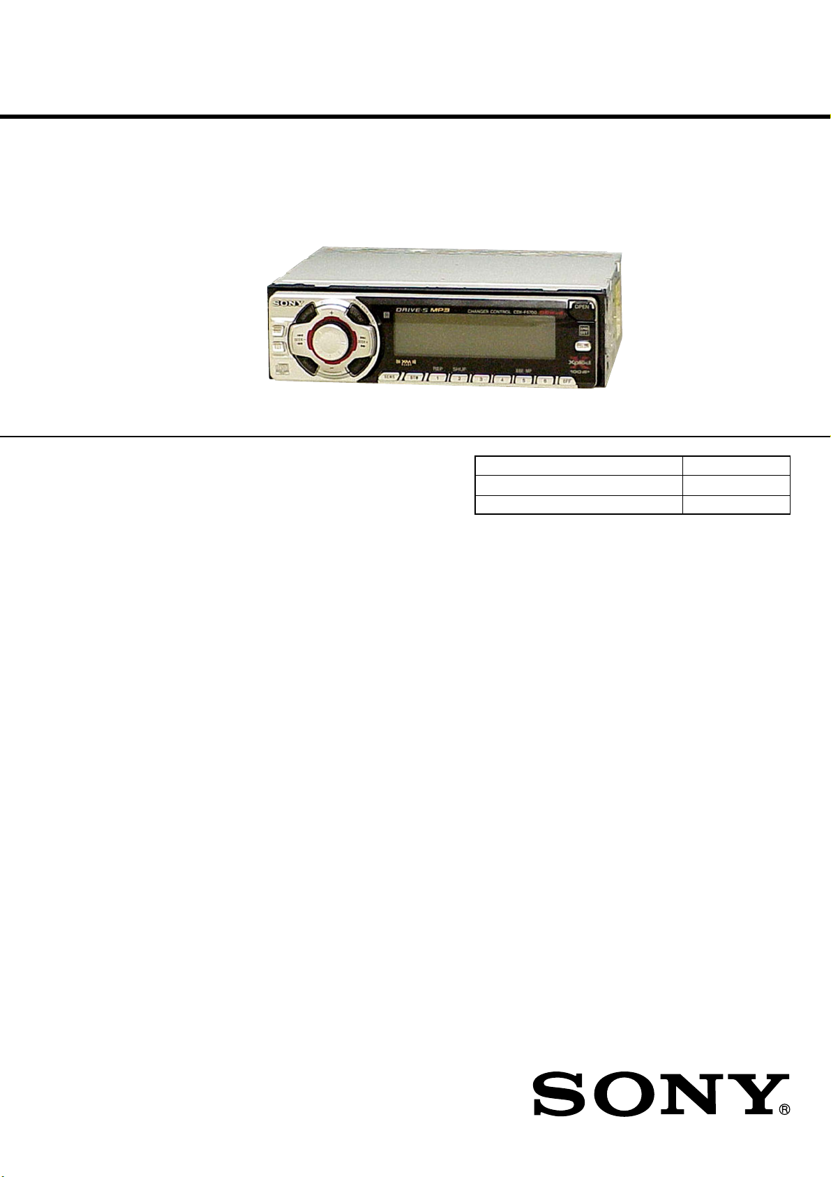
Photo: CDX-F5700
• The tuner and CD sections have no adjustments.
AUDIO POWER SPECIFICATIONS (US MODEL)
POWER OUTPUT AND TOTAL HARMONIC DISTORTION
23.2 watts per channel minimum continuous average power into
4 ohms, 4 channels driven from 20 Hz to 20 kHz with no more
than 5% total harmonic distortion.
SPECIFICATIONS
CD player section
Signal-to-noise ratio 120 dB
Frequency response 10 – 20,000 Hz
Wow and flutter Below measurable limit
Tuner section
FM
Tuning range US, Canadian Model:
87.5 – 107.9 MHz
E Model:
FM tuning interval:
50 kHz/200 kHz
switchable
87.5 – 108 MHz (at 50 kHz step)
87.5 – 107.9 MHz (at 200 kHz step)
Antenna terminal External antenna connector
Intermediate frequency 10.7 MHz/450 kHz
Usable sensitivity 9 dBf
Selectivity 75 dB at 400 kHz
Signal-to-noise ratio 67 dB (stereo),
69 dB (mono)
Harmonic distortion at 1 kHz
0.5% (stereo),
0.3% (mono)
Separation 35 dB at 1 kHz
Frequency response 30 – 15,000 Hz
US Model
CDX-F5700/FW570
Canadian Model
CDX-F5700
E Model
CDX-F5700X
Model Name Using Similar Mechanism NEW
CD Drive Mechanism Type MG-611MA-186//Q
Optical Pick-up Name KSS1000E
AM
Tuning range US, Canadian Model:
530 – 1,710 kHz
E Model:
AM tuning interval:
9 kHz/10 kHz switchable
531 – 1,602 kHz (at 9 kHz step)
530 – 1,710 kHz (at 10 kHz step)
Antenna terminal External antenna connector
Intermediate frequency 10.7 MHz/450 kHz
Sensitivity 30 µV
Power amplifier section
Outputs Speaker outputs
(sure seal connectors)
Speaker impedance 4 – 8 ohms
Maximum power output 52 W × 4 (at 4 ohms)
General
Outputs Audio outputs terminal (front/rear)
Subwoofer output terminal (mono)
Power antenna relay control terminal
Power amplifier control terminal
Inputs Telephone ATT control terminal
Illumination control terminal
BUS control input terminal
BUS audio input or AUX IN terminal
Remote controller input terminal
Antenna input terminal
9-877-605-01
2004B04-1
© 2004. 02
– Continued on next page –
FM/AM COMPACT DISC PLAYER
Sony Corporation
e Vehicle Company
Published by Sony Engineering Corporation
1
CDX-F5700/F5700X/FW570
Tone controls US, Canadian Model:
Bass ±10 dB at 62 Hz
Treble ±10 dB at 16 kHz
E Model:
Bass ±8 dB at 100 Hz
Treble ±8 dB at 10 kHz
Loudness +8 dB at 100 Hz
+2 dB at 10 kHz
Power requirements 12 V DC car battery
(negative ground)
Dimensions Approx. 178 × 50 × 177 mm
(7 1/8 × 2 × 7 in.) (w/h/d)
Mounting dimensions Approx. 182 × 53 × 161 mm
(7 1/4 × 2 1/8 × 6 3/8 in.) (w/h/d)
Mass Approx. 1.2 kg
(2 lb. 10 oz.)
Supplied accessories Parts for installation and connections (1 set)
Front panel case (1)
Card remote commander RM-X114
Note
This unit cannot be connected to a digital preamplifier or an equalizer which is Sony
BUS system compatible.
Design and specifications are subject to change without
notice.
SERVICE NOTES
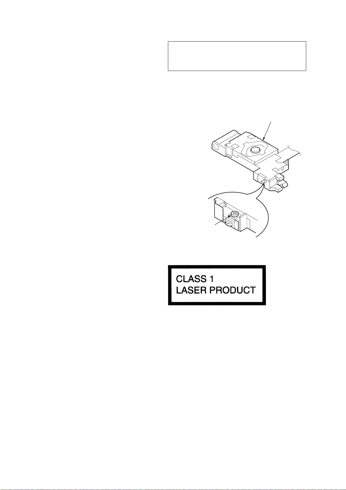
NOTES ON HANDLING THE OPTICAL PICK-UP BLOCK
OR BASE UNIT
The laser diode in the optical pick-up block may suffer electrostatic
breakdown because of the potential difference generated by the
charged electrostatic load, etc. on clothing and the human body.
During repair, pay attention to electrostatic breakdown and also use
the procedure in the printed matter which is included in the repair
parts.
The flexible board is easily damaged and should be handled with
care.
NOTES ON LASER DIODE EMISSION CHECK
The laser beam on this model is concentrated so as to be focused on
the disc reflective surface by the objective lens in the optical pickup block. Therefore, when checking the laser diode emission, observe from more than 30 cm away from the objective lens.
CAUTION
Use of controls or adjustments or performance of procedures
other than those specified herein may result in hazardous
radiation exposure.
If the optical pick-up block is defective, please replace the whole
optical pick-up block.
Never turn the semi-fixed resistor located at the side of optical
pick-up block.
optical pick-up
semi-fixed resistor
• E model
Notes on Chip Component Replacement
• Never reuse a disconnected chip component.
• Notice that the minus side of a tantalum capacitor may be dam-
aged by heat.
TEST DISCS
This set can playback CD-R and CD-ROM discs. The following
test discs should be used to check the capability:
CD-R test disc TCD-R082LMT (Part No. J-2502-063-1)
CD-RW test disc TCD-W082L (Part No. J-2502-063-2)
SAFETY-RELATED COMPONENT WARNING!!
COMPONENTS IDENTIFIED BY MARK 0 OR DOTTED LINE
WITH MARK 0 ON THE SCHEMATIC DIAGRAMS AND IN
THE PARTS LIST ARE CRITICAL TO SAFE OPERATION.
REPLACE THESE COMPONENTS WITH SONY P ARTS WHOSE
PART NUMBERS APPEAR AS SHOWN IN THIS MANUAL OR
IN SUPPLEMENTS PUBLISHED BY SONY.
This label is located on the bottom of the chassis.
ATTENTION AU COMPOSANT AYANT RAPPORT
À LA SÉCURITÉ!!
LES COMPOSANTS IDENTIFIÉS P AR UNE MARQUE 0 SUR LES
DIAGRAMMES SCHÉMATIQUES ET LA LISTE DES PIÈCES
SONT CRITIQUES POUR LA SÉCURITÉ DE FONCTIONNEMENT.
NE REMPLACER CES COMPOSANTS QUE PAR DES PIÈCES
SONY DONT LES NUMÉROS SONT DONNÉS DANS CE MANUEL
OU DANS LES SUPPLÉMENTS PUBLIÉS PAR SONY.
2
CDX-F5700/F5700X/FW570
D
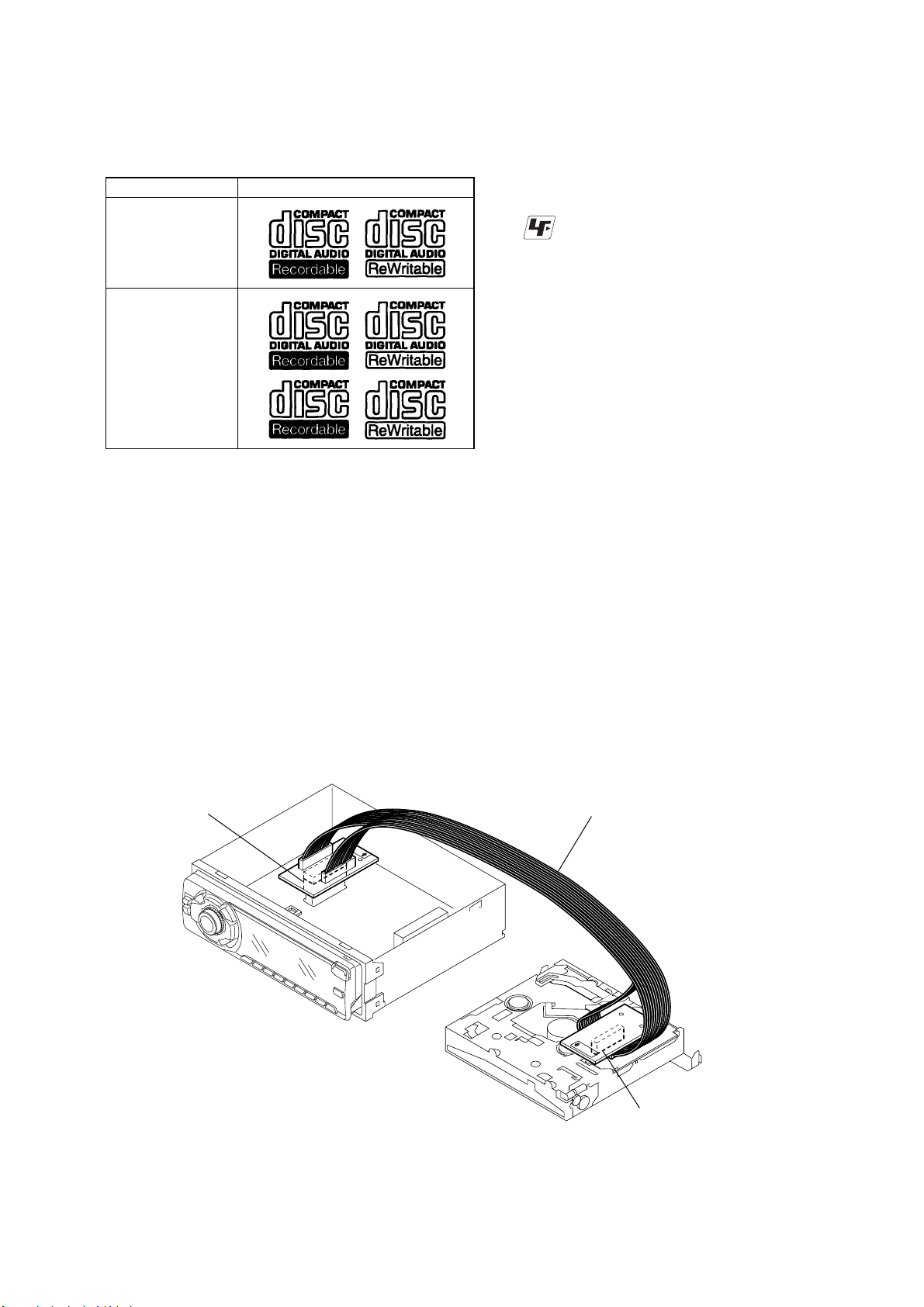
Notes on CD-Rs (recordable CDs)/CD-RWs (rewritable
CDs)
This unit can play the following discs:
Type of discs Label on the disc
Audio CD
MP3 files
• Some CD-Rs/CD-RWs (depending on the equipment used for
its recording or the condition of the disc) may not play on this
unit.
• You cannot play a CD-R/CD-RW that is not finalized∗.
• You can play MP3 files recorded on CD-ROMs, CD-Rs, and
CD-RWs.
• A CD-R/CD-RW to which a session can be added can be played.
z
UNLEADED SOLDER
Boards requiring use of unleaded solder are printed with the lead
free mark (LF) indicating the solder contains no lead.
(Caution: Some printed circuit boards may not come printed with
the lead free mark due to their particular size.)
: LEAD FREE MARK
Unleaded solder has the following characteristics.
• Unleaded solder melts at a temperature about 40°C higher than
ordinary solder.
Ordinary soldering irons can be used but the iron tip has to be
applied to the solder joint for a slightly longer time.
Soldering irons using a temperature regulator should be set to
about 350°C.
Caution: The printed pattern (copper foil) may peel away if the
heated tip is applied for too long, so be careful!
• Strong viscosity
Unleaded solder is more viscous (sticky, less prone to flow)
than ordinary solder so use caution not to let solder bridges
occur such as on IC pins, etc.
• Usable with ordinary solder
It is best to use only unleaded solder but unleaded solder may
also be added to ordinary solder.
∗ A process necessary for a recorded CD-R/CD-RW disc to be
played on the audio CD player.
EXTENSION CABLE AND SERVICE POSITION
When repairing or servicing this set, connect the jig (extension cable)
as shown below.
• Connect the MAIN board (CN350) and the SERVO board (CN2)
with the extension cable (Part No. J-2502-076-1).
MAIN BOARD
CN350
J-2502-076-1
SERVO BOAR
CN2
3

CDX-F5700/F5700X/FW570
1. GENERAL
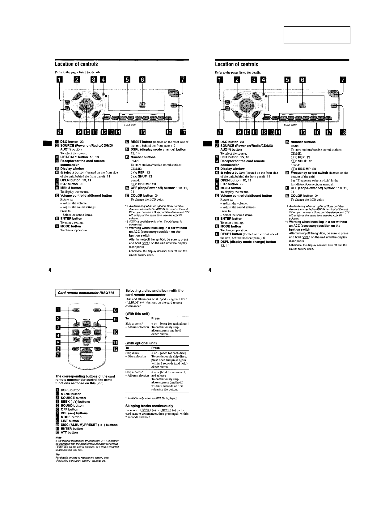
Location of Controls (US, Canadian Model) .......................... 5
Location of Controls (E Model) .............................................. 5
Connections (US, Canadian Model)........................................ 6
Connections (E Model) ........................................................... 7
2. DISASSEMBLY
2-1. Sub Panel Assy.................................................................... 9
2-2. CD Mechanism Block ......................................................... 9
2-3. Main Board ....................................................................... 10
2-4. Chassis (T) Sub Assy ........................................................ 10
2-5. Roller Arm Assy ................................................................ 11
2-6. Chassis (OP) Assy.............................................................11
2-7. Optical Pick-up ................................................................. 12
2-8. SL Motor Assy (M902) .....................................................12
2-9. LE Motor Assy (M903)..................................................... 13
2-10. Servo Board....................................................................... 13
3. DIAGRAMS
3-1. IC Pin Descriptions ........................................................... 14
3-2. Block Diagram –CD Section–........................................... 19
3-3. Block Diagram –Main Section–........................................20
3-4. Block Diagram –Display Section–....................................21
3-5. Circuit Boards Location .................................................... 21
3-6. Note for Printed Wiring Boards and
Schematic Diagrams ..........................................................22
3-7. Waveforms......................................................................... 22
3-8. Printed Wiring Boards –CD Mechanism Section–............ 23
3-9. Schematic Diagram –CD Mechanism Section (1/2)– ....... 24
3-10. Schematic Diagram –CD Mechanism Section (2/2)– ....... 25
3-11. Schematic Diagram –Main Section (1/2)– ........................26
3-12. Schematic Diagram –Main Section (2/2)– ........................27
3-13. Printed Wiring Board –Main Section– .............................. 28
3-14. Printed Wiring Board –Sub Section– ................................ 29
3-15. Schematic Diagram –Sub Section– ...................................29
3-16. Printed Wiring Board –Display Section– .......................... 30
3-17. Schematic Diagram –Display Section–............................. 31
3-18. IC Block Diagrams............................................................ 32
TABLE OF CONTENTS
4. EXPLODED VIEWS
4-1. Main Section ..................................................................... 34
4-2. Front Panel Section ........................................................... 35
4-3. CD Mechanism Section (1) ...............................................36
4-4. CD Mechanism Section (2) ...............................................37
4-5. CD Mechanism Section (3) ...............................................38
4-6. CD Mechanism Section (4) ...............................................39
5. ELECTRICAL PARTS LIST ........................................ 40
4
CDX-F5700/F5700X/FW570
SECTION 1
GENERAL
(US, Canadian Model) (E Model)
This section is extracted
from instruction manual.
5
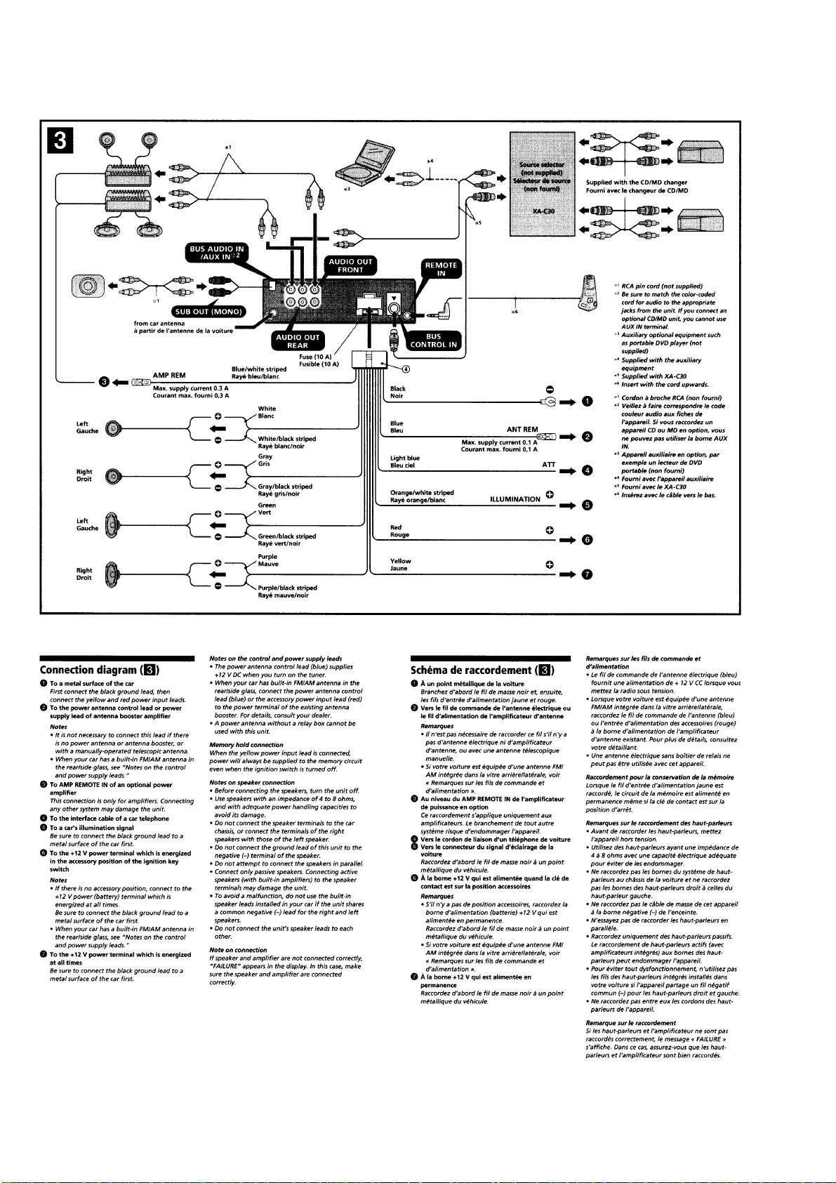
CDX-F5700/F5700X/FW570
Connections (US, Canadian Model)
6
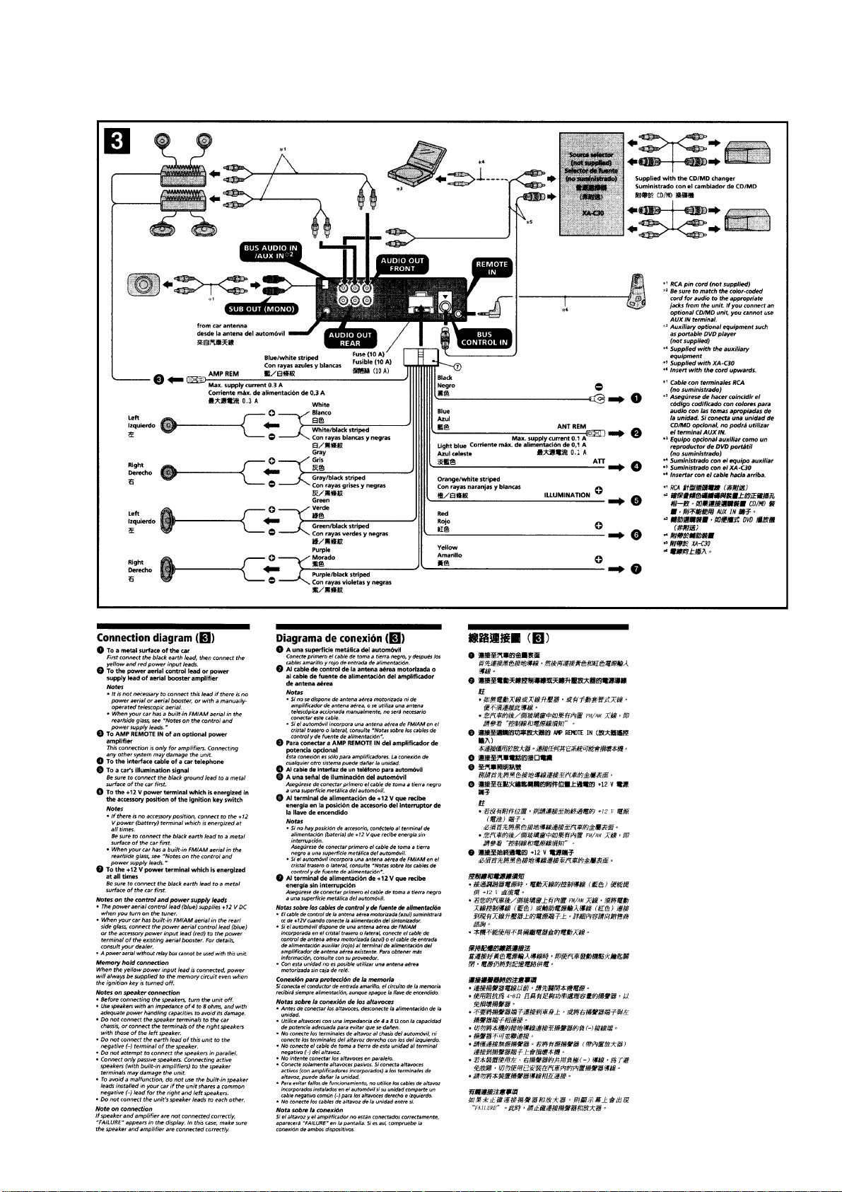
Connections (E Model)
CDX-F5700/F5700X/FW570
7
CDX-F5700/F5700X/FW570
SECTION 2
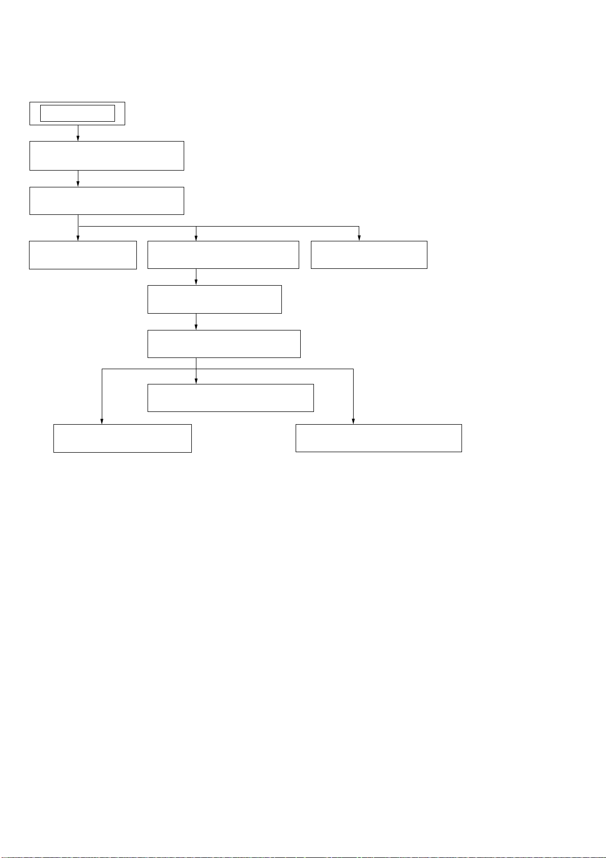
DISASSEMBLY
Note : This set can be disassemble according to the following sequence.
SET
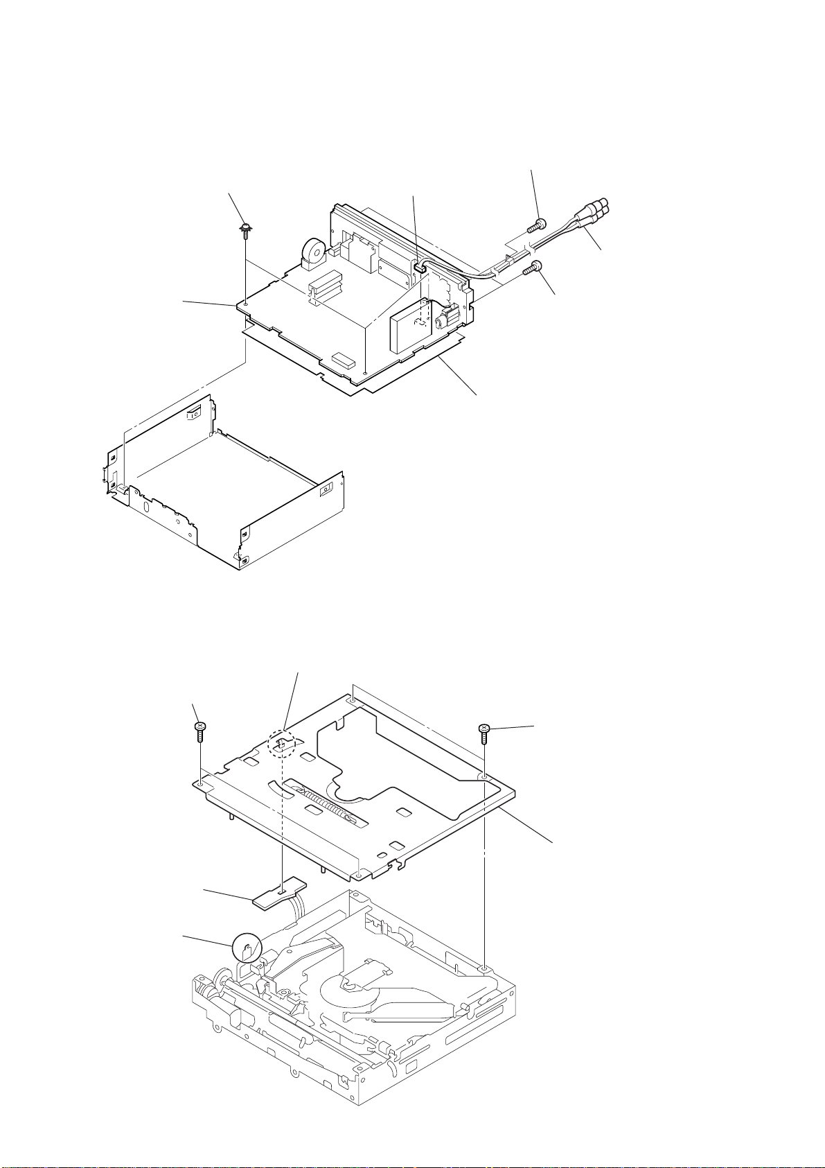
2-1. SUB PANEL ASSY
(Page 9)
2-2. CD MECHANISM BLOCK
(Page 9)
2-3. MAIN BOARD
(Page 10)
2-7. OPTICAL PICK-UP
(Page 12)
2-4. CHASSIS (T) SUB ASSY
(Page 10)
2-5. ROLLER ARM ASSY
(Page 11)
2-6. CHASSIS (OP) ASSY
(Page 11)
2-8. SL MOTOR ASSY (M902)
(Page 12)
2-10. SERVO BOARD
(Page 13)
2-9. LE MOTOR ASSY (M903)
(Page 13)
8
Note : Follow the disassembly procedure in the numerical order given.
s
)
2-1. SUB PANEL ASSY
3
two claws
4
CDX-F5700/F5700X/FW570
2
two claw
1
two
screws
(+PTT 2.6
x
6)
2-2. CD MECHANISM BLOCK
5
CD mechanism block
5
sub panel assy
7
bracket (CD)
CN370
6
two
screws
(+PTT 2.6
x
4)
2
screw
(+PTT 2.6
x
6)
3
4
CN350
1
screw
(+PTT 2.6
x
6
9
CDX-F5700/F5700X/FW570
)
2-3. MAIN BOARD
1
three ground point screws
3
MAIN board
(+PTT 2.6
x
6)
4
CN410
insulating sheet
5
screw
(+PTT 2.6
2
two
(+PTT 2.6
x
6)
6
screws
cord (RCA
x
6)
2-4. CHASSIS (T) SUB ASSY
2
two
screws
(+P 1.7
5
SENSOR board
3
claw
x
2.2)
4
claw
1
two
screws
x
(+P 1.7
6
2.2)
chassis (T) sub assy
10
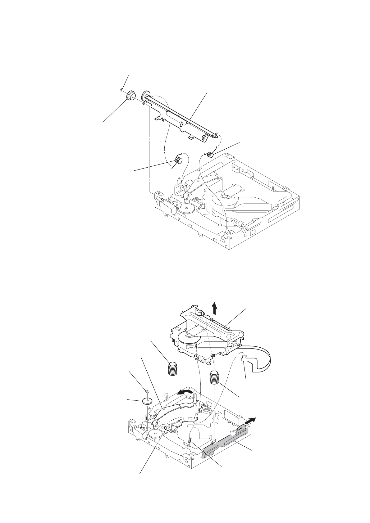
2-5. ROLLER ARM ASSY
4
worm wheel (RA)
1
spring (RAL)
3
washer
5
roller arm assy
CDX-F5700/F5700X/FW570
2
spring (RAR)
2-6. CHASSIS (OP) ASSY
0
coil spring (damper)
4
washer
5
gear (LE1)
lever (D)
6
8
qa
chassis (OP) assy
1
CN1
9
two coil springs (damper)
7
slider (R)
2
Remove the six solderings.
3
tension coil spring (KF)
11
CDX-F5700/F5700X/FW570
)
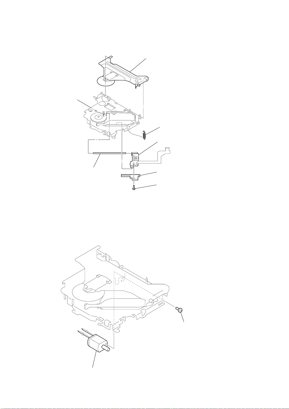
2-7. OPTICAL PICK-UP
5
claw
2
chucking arm sub assy
1
tension coil spring (CHKG
7
optical pick-up
2-8. SL MOTOR ASSY (M902)
6
main shaft
4
rack (SL)
3
screw
(+B 1.4
x
5)
12
2
SL motor assy (M902)
1
screw
(+P 1.4
x
1.8)
2-9. LE MOTOR ASSY (M903)
qf
two toothed lock
(+M 1.4
bracket (LEM)
qs
(+M 1.7
screw
x
)
screws
2.5)
6
screw
(+P 1.7
x
qd
2.2)
qa
screw
(+M 1.7
qg
(M903)
0
woam (LEB) assy
x
2.5)
LE motor assy
7
leaf spring (LE)
8
screw
(+M 1.7
9
bearing (LEB)
2
washer
gear (LE1)
3
lever (D)
CDX-F5700/F5700X/FW570
x
2.5)
4
slider (R)
5
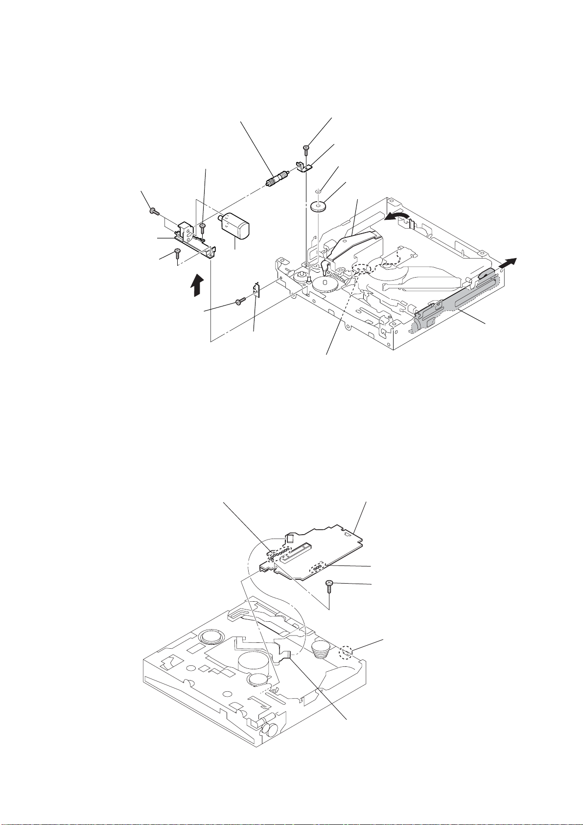
2-10. SERVO BOARD
1
Remove the eight solderings.
1
Remove the soldering.
6
SERVO board
2
Remove the three solderings.
4
toothed lock
(M 1.7)
5
screw
claw
3
CN1
13
CDX-F5700/F5700X/FW570
SECTION 3
DIAGRAMS
3-1. IC PIN DESCRIPTIONS
• IC3 CXD3059BR (DIGITAL SERVO/DIGITAL SIGNAL PROCESSOR) (SERVO BOARD (1/2))
Pin No. Pin Name I/O Pin Description
1MIRR I/O Mirrer signal input/output
2 DFCT I/O Defect signal input/output
3 FOK I/O Focus OK signal input/output
4 VSS — Ground pin
5 LOCK I/O Not used in this set. (Open)
6 MDP O Spindle motor servo control signal output
7 SSTP I Disc most inner detection signal input
8IOVSS1 — Digital ground pin for I/O
9 SFDR O Sled drive signal output
10 SRDR O Sled drive signal output
11 TFDR O Tracking drive signal output
12 TRDR O Tracking drive signal output
13 FFDR O Focus drive signal output
14 FRDR O Focus drive signal output
15 IOVDD1 — Digital power supply pin for I/O
16 AVDD0 — Analog power supply pin
17 AVSS0 — Analog ground pin
18 NC — Not used. (Open)
19 E I E signal input
20 F I F signal input
21 TEI I Tracking error signal input from the DSSP block
22 TEO O Tracking error signal output to the RF amp block
23 FEI I Focus error signal input from the DSSP block
24 FEO O Focus error signal output to the RF amp block
25 VC I/O
26 A I A signal input
27 B I B signal input
28 C I C signal input
29 D I D signal input
30 NC — Not used. (Open)
31 AVDD4 — Analog power supply pin
32 RFDCO I/O
33 PDSENS I Reference volta ge input for PD
34 AC SUM O RFAC suming amp signal output
35 EQ IN I Equalizer circuit signal input
36 LD O APC amp signal output
37 PD I APC amp signal input
38 NC — Not used. (Open)
39 RFC I EQ cut off frequency adjustment input
40 AVSS4 — Analog ground pin
41 RFACO O RFAC signal output
42 RFACI I RFAC signal input or EFM signal input
43 AVDD3 — Analog power supply pin
44 BIAS I Asymmetry circuit constant current input
45 ASYI I Asymmetry comparate voltage input
46 ASYO O EFM full swing signal output
47 VPCO O Charge pump output for wideband EFM PLL
48 VCTL I VCO2 control voltage input for wideband EFM PLL
49 AVSS3 — Analog ground pin
VC voltage output to the RF amp block
Center voltage input from the DSSP block by command select
RFDC signal output
RFDC signal input from the DSSP block by command select
14

CDX-F5700/F5700X/FW570
Pin No. Pin Name I/O Pin Description
50 CLTV I VCO1 control voltage input
51 FILO O Filter signal output for master PLL
52 FILI I Filter signal input for master PLL
53 PCO O Charge pump output for master PLL
54 AVDD5 — Analog power supply pin
55 DDVROUT O DC/DC converter output
56 DDVRSEN I DC/DC converter output voltage monitor signal input
57 AVSS5 — Analog ground pin
58 DDCR I Reset signal input for DC/DC converter
59 NC — Not used. (Open)
60 BCKI I D/A interface bit clock signal input
61 PCMDI I D/A interface serial data signal input
62 LRCKI I D/A interface LR clock signal input
63 LRCK O D/A interface LR clock signal output
64 VSS — Digital ground pin for internal
65 PCMD O D/A interface serial data signal output
66 BCK O D/A interface bit clock signal output
67 VDD — Digital power supply pin for internal
68 EMPH O Not used in this set. (Open)
69 EMPHI I Not used in this set. (Fixed at “L”.)
70 IOVDD2 — Digital power supply pin for I/O
71 DOUT O Digital out signal output
72, 73 TEST I Test pin Normally “L”.
74 IOVSS2 — Digital ground pin for I/O
75 NC — Not used in this set. (Open)
76 XVSS — Ground pin for master clock
77 XTAO O Crystal oscillation circuit output (16.9344 MHz)
78 XTAI I Crystal oscillation circuit input (16.9344 MHz)
79 XVDD — Power supply pin for master clock
80 AVDD1 — Analog power supply pin
81 AOUT1 O L channel analog signal output
82 VREFL O L channel reference voltage output
83 AVSS1 — Analog ground pin
84 AVSS2 — Analog ground pin
85 VREFR O R channel reference voltage output
86 AOUT2 O R channel analog signal output
87 AVDD2 — Analog power supply pin
88 NC — Not used. (Open)
89 IOVDD0 — Digital power supply pin for I/O
90 RMUT O R channel “0” detection flug output
91 LMUT O L channel “0” detection flug output
92 NC — Not used. (Open)
93 XTSL I X’tal select signal input 16.9344 MHz: “L”, 33.8688 MHz: “H”
94 IOVSS0 — Digital ground pin for I/O
95 XTACN I Oscillation circuit control input “H”: Oscillation start, “L”: Oscillation stop
96 SQSO O Sub 80 bit and PCM peak, level data signal output CD text data signal output
97 SQCK I Clock signal input for SQSO read out
98 SBSO O Sub P-W serial data signal output Not used in this set. (Open)
99 EXCK I Clock signal input for SBSO read out Not used in this set. (Open)
100 XRST I System reset signal input “L”: reset
101 SYSM I Mute signal input “H”: mute Not used in this set. (Fixed at “L”.)
102 DATA I Serial data signal input
103 VSS — Digital ground pin for internal
15

CDX-F5700/F5700X/FW570
Pin No. Pin Name I/O Pin Description
104 XLAT I Latch signal input
105 CLOK I Serial data transfer clock signal input
106 VDD — Digital power supply pin for internal
107 SENS O SENS signal output
108 SCLK I Clock signal input for SENS serial data read out
109 ATSK I/O Input/output for anti-shock
110 WFCK O WFCK signal output Not used in this set. (Open)
111 XUGF O XUGF signal output Not used in this set. (Open)
112 XPCK O XPCK signal output Not used in this set. (Open)
113 GFS O GFS signal output
114 C2PO O C2PO signal output
115 SCOR O Sub code sync signal output
116 VDD — Digital power supply pin for internal
117 C4M O 4.2336 MHz signal output Not used in this set. (Open)
118 WDCK O Word clock signal output Not used in this set. (Open)
119 COUT I/O Track count signal input/output Not used in this set. (Open)
120 NC — Not used. (Open)
16

CDX-F5700/F5700X/FW570
• IC600 MN101E01KDG (SYSTEM CONTROL) (MAIN BOARD (2/2))
Pin No. Pin Name I/O Pin Description
1DAVDD — Power supply pin for D/A output converter (+3.3 V)
2 NCO O Not used in this set. (Open)
3DAVSS — Ground pin for D/A output converter
4 UNISO O SONY-BUS data signal output
5 UNISI I SONY-BUS data signal input
6 UNICKO O SONY-BUS clock signal output
7, 8 RE 0, RE 1 I Rotary encoder signal input
9 ILLIN I Illumination signal input for auto dimmer H: Ill off, L: Ill on
10 VDD1 — Power supply pin for internal core (+3.3 V)
11 MMOD I Flash microcomputer write detection signal input
12 OSCOUT O High speed operation clock signal output (27.648 MHz)
13 OSCIN I High speed operation clock signal input (27.648 MHz)
14 VSS1 — Ground pin for internal core
15 XIN I Low speed operation clock signal input (32.768 kHz)
16 XOUT O Low speed operation clock signal output (32.768 kHz)
17 VDD2 — Power supply pin for internal core (+3.3 V)
18 MOD1 — Pull up: “H”
19 RESET I Reset signal input
20 RCIN1 I Rotary shift commander shift key signal input
21 ACC IN I Accessory power supply detection signal input
22 TEST IN I Test mode detection signal input
23 TEL ATT I Telephone attenuate detection signal input
24 ATT O Audio mute control signal output
25 ADON O A/D converter power supply control signal output
26 NCO O Not used in this set. (Open)
27 KEYACK I Key acknowledge detection signal input
28 TU ATTIN I Tuner mute ZERO cross detection signal input
29 CDON I CD mechanism servo power supply control signal input
30 CDMON I CD mechanism loading +6V power supply control signal input
31 BUIN I Back up power supply detection signal input
32 to 35 NCO O Not used in this set. (Open)
36 BUSON O BUS on signal output
37 SYSRST O System reset signal output
38 to 41 NCO O Not used in this set. (Open)
42 Z MUTE I CD mechanism zero cross mute detection signal input
43 to 48 NCO O Not used in this set. (Open)
49 ILL VSEL O Not used in this set. (Open)
50 BBE SEL I BBE with/without setting pin L: with, H: without Not used in this set. (Open)
51 AREASEL2 I Destination function setting input 2 Not used in this set. (Open)
52 AREASEL1 I Destination function setting input 1
53 AREASEL0 I Destination function setting input 0
54 to 57 NCO O Not used in this set. (Open)
58 DOOR SW I Front panel open/close detection signal input “L”: Panel close, “H”: Panel open
59 DIAG I Condition signal input from the power IC
60 VOLATT O Electronic volume attenuate control signal output
61 NOSE SW I Front panel attachment detection signal input L: Panel on
62 AUX IN O AUX light change signal output L: AUX, H: BUS in
63 VSS2 — Ground pin for I/O port
64 TU ATT O Tuner mute control signal output
65 NCO (TUON) O Not used in this set. (Open)
66 NS MASK O AEP, UK model: Noise mask signal output US, Canadian, E model: Not used. (Open)
67 E2P CKO O Serial clock signal output for EEPROM communication
17

CDX-F5700/F5700X/FW570
Pin No. Pin Name I/O Pin Description
68 E2P SIO I/O Serial data signal input/output for EEPROM communication
69 DOORIND O Sub panel power supply control signal output
70 AMPSTB O Power regulator IC standby signal output
71 NCO O Not used in this set. (Open)
72 LCDSO O Serial data signal output to the LCD driver Flash: UART serial output
73 LCDCE O Chip enable signal output to the LCD driver Flash: Serial input
74 LCDCKO O Serial clock signal output to the LCD driver
75 to 78 NCO O Not used in this set. (Open)
79 I2C SIO I/O I2C BUS serial data signal input/output
80 NCO O Not used in this set. (Open)
81 I2C CKO O I2C BUS serial clock signal output
82 DAVN I
83 SIRCS I Remote control signal input
84 NCO O Not used in this set. (Open)
85 BEEP O Beep signal output to the power amp
86 to 88 NCO O Not used in this set. (Open)
89 VDD3 — Power supply pin for I/O port (+3.3 V)
90 NCO O Not used in this set. (Open)
91 VSS3 — Ground pin for I/O port
92 QUALITY I AE P, UK model: Noise detection signal input US, Canadian, E model: Not used. (Open)
93 VSM I S meter voltage detection signal input
94 KEYIN1 I Key signal input 1
95 KEYIN0 I Key signal input 0
96 RCIN0 I Rotary commander signal input
97 SA IN I Spectrum analyzer signal input
98 SA CLK O Spectrum analyzer clock signal output
99 NCO O Not used in this set.
100 VREF+ — Power supply pin for A/D input converter
AEP, UK model: RDS data block synchronization detection signal input
US, Canadian, E model: Not used. (Open)
18

3-2. BLOCK DIAGRAM — CD SECTION —
DETECTOR
PD1
PD2
E
F
LASER DIODE
PICK-UP BLOCK
(KSS1000E)
2-AXIS DEVICE
(FOCUS)
(TRACKING)
PD LD
OPTICAL
PD2
PD1
I-V AMP
PD
FCS+
FCS–
TRK+
TRK–
RFACO
A
26
B
27
C
28
D
29
E
F
LD
AUTOMATIC
CONTROL
M902
(SLED)
M901
(SPINDLE)
M903
(LOADING)
POWER
Q1
M
M
M
19
E
20
F
36
LD
FOCUS/TRACKING COIL DRIVE,
SLED/SPINDLE/LOADING
MOTOR DRIVE
11
VO2–
10
VO2+
13
VO1–
12
VO1+
6
VO4+
7
VO4–
8
VO3+
9
VO3–
5
VLO+
4
VLO–
FEO
TEO
IC1
CDX-F5700/F5700X/FW570
• R-ch is omitted due to same as L-ch.
• Siganal Path
: CD PLAY
ASYO
41
24
22
37
PD
VIN2+
VIN2–
VIN1+B
VIN1–B
VIN4+
VIN4–
VIN3+
MUTE
FWD
REV
RFACI
42
FEI
23
TEI
21
22
21
19
18
31
32
25
34
1
2
46
RF AMP,DIGITAL SERVO,
DIGITAL SIGNAL PROCESSOR
IC3
ASYI
45
FFDR
13
FRDR
14
TFDR
11
TRDR
12
SFDR
9
SRDR
10
MDP
6
AOUT1
AOUT2
LMUTE
RMUTE
FOK
SQSO
SQCK
XRST
DATA
XLAT
CLOK
SENS
SCLK
GFS
C2POT
SCOR
XTAI
XTAO
BCK
BCKI
PCMDI
LRCK
LRCKI
PCMD
100
102
104
105
107
108
113
114
115
81
86
R-CH
91
90
3
96
97
78
77
66
60
61
63
62
65
X1
16.934MHz
SW1
(DOWN)
SW2
(SELF)
SW3
(DISC IN)
SW4
(LIMIT)
X2
18.43MHz
CD LMUT
22
CD RMUT
23
CD FOK
19
CD SQSO
16
CD SQCK
18
CD XRST
15
CD DATA
14
CD XLAT
13
CD CLOK
12
CD SENS
11
CD SCLK
10
CD GFS
8
CD C2PO
7
CD SCORT
52
X1
81
X0
80
MEC_DSW
46
MEC_SELFSW
53
MEC_INSW
45
MEC_LIMIT
42
DRON
41
MEC LOAD
43
MEC EJECT
44
CD
SYSTEM CONTROL
IC4
UNISI
RXD
UNISO
TXD
UNICLK
BUS ON
BU IN
RSTX
A ATT
LINK OFF
EJECT OK
MECON
CDON
ZMUT
MECON CHK
CDON CHK
DECON
DEC XMUTE
DEC SSTBY
DEC XRST
DEC STBY
DEC INT
DEC SCL
DEC SDA
EMPH
56
25
57
26
58
50
51
75
60
20
SYSTEM CONTROL
61
63
64
66
67
68
+1.5V
65
37
27
28
29
30
31
32
69
MECHA+6V
SERVO+3.3V
+1.5V
CONTROL
Q2,3
+3.3V
DOOR W
58
CDM ON
30
CD ON
29
Z MUTE
42
+1.5V REG
IC7
VOUT
+3.3V
CONTROL
Q5,6
CLCK
22
SRMSTB
41
RESET
2
STANDBY
3
BUCK
36
I2C SCL
7
I2C SDA
6
BUSO
28
CD-L
UNI SI
UNI SO
UNI SCK
BUS ON
BU IN
SYS RST
ATT
LINK OFF
IC600 (1/3)
VDD
15
CE
3
AUDIO INTERFACE
IC8
MAIN
A
SECTION
(Page 20)
MAIN
B
SECTION
(Page 20)
U COM+3.3V
19 19
15
18
11
16
19
14
BCK1A
BCK1B
SD0O
LRCK1A
LRCK1B
SD1O

CDX-F5700/F5700X/FW570
3-3. BLOCK DIAGRAM — MAIN SECTION —
J451(1/2)
L
BUS
AUDIO IN
R
TU1
(TUNER UNIT)
J1
(ANTENNA)
1
ANT
VCC
VDD+5V
E2P VDD
SCL
SDA
S-METER
TU MUTE
E2P SCL
E2P SDA
R
L
R-CH
4
3
10
11
15
13
14
6
7
16
17
SELECT SWITCH
AUDIO+8.3V
TU+5V
BACK UP+3.3V
SCL
SDA
CD
SECTION
(Page 19)
BUS AUDIO
Q351
B
UNI SO
UNI SI
UNI SCK
BUS ON
SYS RST
CD
SECTION
(Page 19)
D353
CD-L
A
D609 D610
D354
R-CH
R-CH
SOUND CONTROL,
ELECTRONIC VOLUME
IC351
OUTLR
4
7
5
42
43
40
41
14
16
97
98
62
93
64
67
68
4
5
6
36
37
IN1L+
IN1R+
IN1-
IN3L
IN3R
IN4L
IN4R
SACLK
SAOUT
SAIN
SACLK
AUXIN
VSM
TU ATT
E2P CKO
E2P SIO
UNI SO
UNI SI
UNI SCK
BUS ON
SYS RST
OUTLF
OUTSW
OUTRF
OUTRR
SYSTEM CONTROL
IC600 (2/3)
I2C CKO
I2C SIO
VOL ATT
AMPSTB
KEYACK
ACC IN
TEL ATT
TEST IN
RCIN1
RCIN0
MUTE
SCL
SDA
ATT
BEEP
DIAG
ADON
ILL IN
BUIN
24
25
17
22
21
15
13
12
81
79
60
24
85
70
59
27
25
21
9
23
22
20
96
31
R-CH (FRONT)
R-CH (REAR)
SCL
SDA
SCL
SDA
KEY ACKNOWLEDGE SWITCH
10
13
12
11
8
9
Q501
BUS INTERFACE
IC601
BUIN
RST
BUS IN
CLK IN
DATA OUT
DATA IN
D495 D494
BATT
CLK
DATA I/O
BUS ON
RST
MUTE DRIVE
Q491,492
3
4
6
1
2
MUTE
Q352
MUTE
Q440
MUTE
Q452
D491
ILL CHECK
Q703
OVER VOLTAGE
DETECT
Q605
BUS ON
SWITCH
Q600,601
SDA
SCL
BATT
BATT
12
IN-FL
11
IN-RL
MULTIPLE VOLTAGE
2
SDA
4
SCL
16
BEEP
22
STB
25
DIAG
35
VP
(REMOTE IN)
D602
BATT
BATT
TH400
BACK UP+3.3V
POWER AMP,
REGULATOR
IC300
SERVO+3.3V
MECHA+6V
ACC CHECK
TEL ATT
J390
4
5
6
TU+5V
OUT-FL+
OUT-FL–
OUT-RL+
OUT-RL–
AMP-REM
ANT-REM
AUDIO+B
BU+B
PANEL+B
Q702
Q701
8
3
2
1
7
CN410
5
3
9
7
29
27
BATT
30
AUDIO+8.3V
37
BACK UP+5V
31
SERVO+3.3V
33
MECHA+6V
34
PANEL+9V
CNJ400
(BUS CONTROL IN)
TU+5V REG
Q3
+3.3V REG
IC501
R-CH
R-CH
R-CH
F901
AUDIO+8.3V
BACK UP+5V
J451(2/2)
L
AUDIO OUT
REAR
R
L
AUDIO OUT
FRONT
R
L
SUB
(M0N0)
OUT
R
CN300
1
FL+
9
FL–
2
RL+
10
RL–
4
FR+
12
FR–
3
RR+
11
RR–
5
AMP-REM
6
ANT-REM
16
BATT
7
ACC
14
ILL
13
ATT
15
TEST
• R-CH is omitted due to same as L-CH.
• Signal Path
: CD PLAY
: FM
: AM
: BUS AUDIO
DISPLAY
SECTION
(Page 21)
BU IN
ATT
LINK OFF
RESET
C
2020

3-4. BLOCK DIAGRAM — DISPLAY SECTION — 3-5. CIRCUIT BOARDS LOCATION
t
CDX-F5700/F5700X/FW570
BACK UP+3.3V
MAIN
SECTION
(Page 20)
ROTARY
ENCODER
S921 (1/2)
KEY MATRIX
S911-920,
S921 (2/2)
KEY MATRIX
S801,S901-910
2
RESET
C
LED801,802
RESET
IC602
VOUT
IN
1
DOOR IND
SWITCH
Q101
S103
(RESET)
S102
(NOSE DET)
SYSTEM CONTROL
IC600 (3/3)
RE 0
7
RE 1
8
KEYIN1
94
KEYIN0
95
DOORIND
69
RESET
19
NOSESW
61
LCD SO
LCD CKO
LCD CE
LCD DRIVER
IC901
15
SEG01
I
I
30
SEG16
•
33
72
100
LCD DATA
99
98
CLK
LCD CLK
CE
LCD CE
74
73
SEG17
I
I
86
SEG70
COM1
90
I
|
COM4
87
DIMMER
1
AMBER2
2
AMBER1
3
BLUE1
4
GREEN2
5
GREEN1
6
+3.3V
REG
3 2
IC981
LCD901
LIQUID
CRYSTAL
DISPLAY
PANEL
DIMMER
CONTROL
Q906-908
LED DRIVE
Q901-905
PANEL+5V
LED931-934
LCD
()
BACK LIGHT
PANEL+5V
LED901-922
SENSOR board
DISPLAY board
SERVO board
tuner uni
(TU1)
MAIN board
SUB board
F5700X
S501
FREQUENCY
SELECT
10k
9k
BACKUP+3.3V
X501
32.768kHz
53
15
16
AREASELO
XIN
XOUT
SIRCS
OSCIN
OSCOUT
83
13
12
1
VCC
2
OUT
REMOTE CONTROL
SIGNAL RECEIVER
IC971
X500
27.648MHz
IR
21 21

CDX-F5700/F5700X/FW570
3-6. NOTE FOR PRINTED WIRING BOARDS AND SCHEMATIC DIAGRAMS 3-7. WAVEFORMS
THIS NOTE IS COMMON FOR PRINTED WIRING
BOARDS AND SCHEMATIC DIAGRAMS.
(In addition to this, the necessary note is printed
in each block.)
For schematic diagrams.
Note:
• All capacitors are in µF unless otherwise noted. pF: µµF
50 WV or less are not indicated except for electrolytics
and tantalums.
• All resistors are in Ω and 1/
specified.
f
•
• C : panel designation.
• A : B+ Line.
• B : B– Line.
• H : adjustment for repair.
•Voltages and waveforms are dc with respect to ground
• CD mechanism section (1/2), (2/2)
no mark : CD PLAY
• Main (1/2), (2/2) and Display sections
no mark : FM
: internal component.
Note:
The components identified by mark 0 or dotted
line with mark 0 are criti-
cal for safety.
Replace only with part
number specified.
under no-signal (detuned) conditions.
(): AM
<>: CD PLAY
4
W or less unless otherwise
Note:
Les composants identifiés par
une marque 0 sont critiques
pour la sécurité.
Ne les remplacer que par une
piéce portant le numéro
spécifié.
∗ : Impossible to measure
•Voltages are taken with a VOM (Input impedance 10 MΩ).
Voltage variations may be noted due to normal production tolerances.
•Waveforms are taken with a oscilloscope.
Voltage variations may be noted due to normal production tolerances.
• Circled numbers refer to waveforms.
• Signal path.
J : CD PLAY
F : FM
f : AM
L : BUS AUDIO
• Abbreviation
CND : Canadian model.
For printed wiring boards.
Note:
• X : parts extracted from the component side.
• Y : parts extracted from the conductor side.
a
•
• : Pattern from the side which enables seeing.
(The other layers' patterns are not indicated.)
Caution:
Pattern face side: Parts on the pattern face side seen from the
(Side B) pattern face are indicated.
Parts face side: Parts on the parts face side seen from the
(Side A) parts face are indicated.
• Abbreviation
: Through hole.
C
Q
These are omitted
EB
E
CB
These are omitted
C
BE
These are omitted
CND : Canadian model.
— Servo Board —
(MODE: CD PLAY)
1
Approx. 100mVp-p
wa
(TEI)
IC3
2
Approx. 100mVp-p
wd
(FEI)
IC3
3
IC3
(A), wk (C)
wh
4
IC3
(B), wl (D)
wj
5
IC3
(RFACO)
ra
6
16.9344MHz
IC3 uj (XTAO)
7
0V
0V
Approx.
150mVp-p
Approx.
150mVp-p
Approx.
0.8Vp-p
2Vp-p
1Vp-p
— Main Board —
1
27.648MHz
IC600 qs (OSCOUT)
2
32.768kHz
IC600
(XOUT)
qh
2.2Vp-p
1.8Vp-p
18.43MHz
IC4 ia (X1)
2222

3-8. PRINTED WIRING BOARDS — CD MECHANISM SECTION — • Refer to page 21 for Circuit Boards Location. : Uses unleaded solder.
CDX-F5700/F5700X/FW570
A
B
C
D
E
F
G
H
1
Q6
C83
C74
C85
R116
R149
C92
R145
R142
R143
R141
R140
R85
C1
C2
R117
234567891011 12 13 14
Q5
R107
C22
C24
C42
C81
R39
R148
R70
R22
R24
C60
R37
R147
C39
R42
C23
R23
C25
C30
R25
C34
R41
R43
R55
R54
C50
C57
C107
X2
R146
C35
R124
R133
C32
R38
C40
C38
C49
R61
C64
C46
C47
C6
R12
FB2
R49
C63
Q1
C10
R45
R72
C37
R53
R79
C48
R7
R44
R46
C44
C43
C65
FMB7
R1
C4
CN1
C5
FMB8
R101
R139
R106
IC7
IC8
R111
C75
R64
C56
R18
R123
C19
C91
C115
C86
Q3
R110
IC4
Q2
C33
R126
R40
C77
R109
R56
R92
C58
C54
R52
R91
R16
R29
R50
R47
C36
R60
C29
C28
C41
R77
X1
C59
R48
R136
R114
R5
C8
C27
R68
R76
CN2
R6
BP2
R13
BP3
IC3
C55
R78
C53
C52
R98
R97
R65
FB5
R4
C7
C26
R26
R57
R81
R119
R62
R73
R27
C45
R59
R9
R129
R67
R115
R17
R21
R3
R28
R19
C18
C67
R128
R71
R74
R69
R2
FB1
C79
R127
R87
R80
R8
R20
R108
C51
R86
BP1
R122
C66
C110
R99
R144
C109
SW3
SW2
(Page 28)
C21
C3
R14
R15
C11
IC1
C14
C13
SW1
R11
C16
R10
23 23
• Semiconductor
Location
Ref. No. Location
IC1 G-2
IC3 C-10
IC4 E-2
IC7 B-2
IC8 C-2
Q1 C-4
Q2 B-2
Q3 B-2
Q5 A-2
Q6 A-2

CDX-F5700/F5700X/FW570
3-9. SCHEMATIC DIAGRAM — CD MECHANISM SECTION (1/2) — • Refer to page 22 for Waveforms.
C45
R50
R149
R48
C33
TP344
TP65
TP343
TP94
TP63
TP62
TP59
TP60
TP57
R64
TP61
R29
C29
C28
TP140
R13
R6
R22
C22
C23
CN1
TP21
TP22
TP23
TP24
TP25
TP26
C4
TP27
TP28
TP29
TP30
R1
TP32
TP33
C5
TP34
TP35
C24
C25
BP2
R24
TP71
BP3
R25
R23
C6
TP50
C27
Q1
TP44 TP45
R12R7
C30
C10
TP96
C35
TP97
R38
R52
C41
R40
TP127
TP99
TP116
IC3
R42
R43
R45
C39
C42
C40
R49
R46
C44
C43
R44
TP98
C37C34
R41
C38
TP137
C46
TP141
R53
R59
R67
R60
R56
R71
C54
TP180
C52
C58
C53
C59
TP181
C81
R70
TP167 C55
TP175
R68
R72
C50
R61
R54
R55
C47
C49
C48
C107
C65
C64
R77
X1
C57
R78
R76
R79
R97
C60
R98
CN2
TP129
TP72
TP123
TP128
TP139
TP53
R65
TP56
TP55
R114
R133
R124
TP54
TP48
TP49
TP47
TP133
TP135
TP42
TP51
TP37
TP41
TP132
TP136
TP46
TP36
TP39
TP38
TP43
TP40
(Page 27)
FB2
FB5
(Page 25)
2424

• Refer to page 22 for Waveform.
3-10. SCHEMATIC DIAGRAM — CD MECHANISM SECTION (2/2) — • Refer to page 32 for IC Block Diagrams.
CDX-F5700/F5700X/FW570
(Page 24)
FB1
SW3
SW2
SW1
M903
M901
M902
TP7
TP8
TP9
TP11
TP12
TP19
TP20
TP17
TP18
TP13
TP14
TP15
TP16
R147
IC4
R127
R57
R128
R129
R146
R69
TP52
R62
C51
R119
C67C56
R81
R85
R86
R87
R140
C66
R145
R141
R142
R143
TP31
R74
R80
R115
R91
R92
R39 R73
R136
C36
C63SW4
R14R15
C1
C2
C3
C11
C16
R9
R11
C14
IC B/D
IC1
R8
R117
C21
R18
C19
R20
R19
R17
C18
R123
R21
R28
R27R26
C26
R4
C7
R16
R10
R2
R3
C8
R5
C13
X2
R37
C32
TP58
R47
R148
R122
R126
C86
C115
R110
C75
R144
R108
R109
R99
C77
TP226
C79
TP230
TP231
TP249
R111
C91
C92
C109
IC8
C110
R116
BP1
R107
IC B/D
C83
Q6
C74
IC7
C85
Q3Q5
R106R101
R139
Q2
25 25

CDX-F5700/F5700X/FW570
3-11. SCHEMATIC DIAGRAM — MAIN SECTION (1/2) — • Refer to page 32 for IC Block Diagrams.
F901
CN300
C701
L300
R701
R710
R705
R709
D607
C704
D703
C317
IC B/D
C319
R302
R301
D707
D704
C318
C902
D701
D702
C703
D705
R711
Q703
R712
C303
C302
R702
R703
R704
C454 C434
D706
Q701
C901
Q702
R707
C702
R706
R708
IC300
3
L902
*
0
(F5700/FW570)
2.2
JC302
C304C424C444C301
D305D306D307D308D309D310D311D312
R491
C308
C306
C305 C307 C309
C315
C316
D302
D301
C313
C491
1
*
2
*
C314
Q491
*
Q492
DTC144EKA
DTC114EKA
R365
(F5700/FW570)
0
4.7
(F5700X)
D303 D304
D491
1
Q492
(F5700/FW570)
(F5700X)
C312
D494
D495
C320
C310
3
*
2.2
L902
L901
C433 C453
C351
C443C423
C357
R365
*
R443R423
R453R433
R441
R352
C358
R363
2
(F5700X)
J451
C442 C422 C452 C432 C413 C414
Q432Q440 Q452Q420
R447 R448 R449 R450
C355
C352
R444
C360
C441
C354
R421R442
C421
R446R445
R353
C356
R431R451
C431C451
C359
R362
R354
IC351
C353
R364
C363
C364
C368
C362
C361
Q352
R452
Q351
D352
R360
R357
R359
R355 R356
C365
C366
IC B/D
R358
CN410
C367
R361
C371
C369
J1
F5700/FW570
JC52
C372
R4
R5
Q3
C5
C6
R10
C7
R12
D2
R13
R6
R7
C4
1000p
F5700X
L4
C8
TU1
C2
C3
C9
(Page 27)
2626

• Refer to page 22 for Waveforms.
3-12. SCHEMATIC DIAGRAM — MAIN SECTION (2/2) — • Refer to page 33 for IC Block Diagram.
CDX-F5700/F5700X/FW570
(Page 26)
IC501
D354
R351
L404
L405
C405
D353
L407
L403
L408
L406
C409
C407
C417
C415
C416
(Page 24)
CN350
C412
C401
C403
R402
L410
R401
C402
L401
L402
L409
R520
R525
S501
C420
R534
D501
R501
Q501
R522
R536
C500
R537
R514
R508
C512
C507
X501
R506
R535
C502
R513
R512
R511
R510
R509
R532
R533
C513
R500
R507
R530
C501
C511
C510
X500
C504
R503
C506
C505
IC602
L501
R517
R542
R545R544
R516
R524R523
R547
R548
R549
R560
R561
R528
R529
C904
R526 R527
R546
IC600
R538
R531
R518
C514
J370
R608
Q600
TH400
Q601
CNJ400
R610
R611
C600
D606
C329 D901 D604
L301
L302
L303
R371
R370
D605
R607
R604 R603
R606
D603
D602
IC601
IC B/D
Q605
C601
D610
R602
D609
R601
R110 R111
Q101
R112 R113
S103 S102
27 27
C515
C516 C517 C521 C518 C519
R101
R102
R103
R104
R105
R106
R107
R108
D102
R109
C325
D101
R115
C330
R116
D106
JC110
D103
R120
L100
R121
CN370
(Page 29)

CDX-F5700/F5700X/FW570
3-13. PRINTED WIRING BOARD — MAIN SECTION — • Refer to page 21 for Circuit Boards Location. : Uses unleaded solder.
A
B
C
D
E
F
G
H
J
1
J1
TU1
R12
R13
C8
C4
JC52
570
F5700/FW
I
2
JW1JW
234567891011 12 13 14
J451
J370
CNJ400
R401
C513
R535
C412
JW57
33
JW
IC602
R712
32
JW
R710
D302
D301
CN350
Q702
CN300
F901
D707
D701
D354
D353
R708
C902
19
JW
R711
31
JW
29
JW
D702
R706
JC702
D609
D610
JW20
D704
D705
L407
C416
JW
R702
C417
L404
C415
C401
C702
21
JW
R709
R701
C407
C402
125
D703
D304
D303
JW
C405
C409
75
L405
JC101
JW
L301
D901
C329
R611
122
C701
C704
Q703
63
JW
R707
JW
JW
C901
D706
JW
L403
R351
JW
27
26
76
JC703
JW
JW
JW
28
L406
60
59
58
D606
D607
74
JW
73
JW
R705
72
JW
71
JW
70
JW
68
JW
67
JW
JW
L408
JW
127
JW
JC704
IC601
JW
123
JW
D605
L300
C600
603
R
69
JW
66
65
JW
R608
24
Q600
Q601
JW
JC601
25
JC605
D602
Q605
JC604
TH400
JC608
R610
L303
R604
D603
R606
R607
L302
R371
R370
(Page 23)
• Semiconductor Location
Ref. No. Location
D2 F-2
D101 J-3
D102 J-2
D103 J-3
D106 J-3
D301 D-8
D302 D-8
D303 D-9
D304 D-9
D305 D-6
D306 D-6
D307 D-6
D308 D-6
D309 D-6
D310 D-6
D311 D-7
D312 D-7
D352 B-2
D353 G-8
D354 G-8
D491 F-6
D494 F-8
D495 G-8
D501 I-5
R601
R602
C601
D604
22
D602 F-10
D603 F-11
D604 I-10
D605 C-10
D606 C-10
R113
S102
D607 D-10
D609 H-9
D610 H-9
D701 C-8
JW
R512
C501
JC408
54
R513
56
JW
C363
R525
R530
18
JW
D311
L401
C364
JC510
34
JW
R112
L409
R536
R511
JC508
X501
17
JW
JC302
121
JW
79
JW
L410
Q701
R704
R510
C403
JC51
JC501
301
JW
78
JW
L402
R402
D494
D495
S103
C703
R703
R509
JC300
JC304
Q351
D352
R360
C368
CN410
C369
R452
C372
Q352
C362
C361
R4
45
JW
C6
L4
R6
R7
C2
C3
C9
C5
JC103
C413
R361
47
JW
103
JW
C365
JC1
C371
JC102
R10
48
JW
D102
C7
Q3
JC108
JC109
JC110
C325
R116
D103
104
JW
JW
JW
R5
D2
49
JW
R107
R108
CN370
C414
R359
107
132
42
JW
D101
R358
JW92
R357
R355
C367
C366
JC93
JC90
D106
JW
R105
JC401
JC400
JC404
R356
5
R106
R115
R443
C352
JC306
C355
JC307
C354
C356
JW
JW
JW
JW
R109
L100
106
105
JW
50
C452
C351
C353
JW
62
R302
C330
R120
R442
52
133
C443
R433
R526
R121
C432
C441
JW
4
JW
JW
R423
R450
Q452
R365
R363
JC105
Q440
C433
JC17
R364
40
JW
C319
137
129
C358
C357
R104
R101
R451
6
JW
C442
Q432
R352
JC16
R538
R529
R453
C451
IC351
R447
C423
R449
R362
C453
R528
38
JW
R421
R103
R448
C422
R441
C303
C421
134
JW
37
JW
7
JW
R111
R110
R431
R445
R444
Q420
C302
R548
JW
R102
8
JW
JC301
C424
C431
R446
C360
R524
108
C444
JW
R527
51
JW
R353
R549
Q101
JW
JW
C359
JW
91
JC507
L902
102
101
JW
R523
10
JW
R533
136
90
JC512
C904
JC502
C312
L901
C308
R354
JW
JW
36
JW
C309
C320
JW
JW
JW
C310
JC504
C306
135
JW
C317
R301
C318
401
93
JW
89
R560
35
R561
JW
C516
C515
14
12
JW
JW
C517
C519
43
JW
C307
JW
JC49
S501
C420
61
JW
112
111
113
JW
C514
D501
110
C305
R501
130
JC305
114
JW
D308
C314
88
JW
15
JW
R545
R516
C518
87
JW
R491
R522
R547
R518
R534
86
JW
R544
R517
JC509
C505
IC600
C500
C521
D307
C315
C313
D491
R520
IC300
115
JW
Q491
R500
C304
116
JW
D305
C316
JC503
R542
FMB3
FM
C504
JW
B4
126
JW
C301
C434
117
C454
JW
118
119
120
JW
JW
C512
IC501
R531
Q501
Q492
JC505
JW
JW
X500
C507
C502
JW
JW
JW
JW
R514
53
3
R508
C511
JW
JW
JW
82
83
84
85
JC506
R537
D312
80
81
C510
D306
16
D310
C491
C506
94
JW
R546
R506
JC104
JW39
D309
L501
R507
R532
Ref. No. Location
D702 E-9
D703 C-9
D704 C-9
D705 D-9
D706 C-9
D707 C-8
D901 B-10
IC300 B-6
IC351 F-4
IC501 E-7
IC600 H-6
IC601 I-10
IC602 H-8
Q3 F-2
Q101 H-4
Q351 B-2
Q352 D-2
Q420 C-4
Q432 C-4
Q440 C-4
Q452 C-4
Q491 F-6
Q492 F-7
Q501 H-7
Q600 H-10
Q601 G-10
Q605 F-10
Q701 G-8
Q702 H-8
Q703 E-9
(Page 29)
2828

3-14. PRINTED WIRING BOARD — SUB SECTION — • Refer to page 21 for Circuit Boards Location. : Uses unleaded solder.
CDX-F5700/F5700X/FW570
A
B
C
D
1
23456
(Page 30)
LED802
CN801
(Page 28)
CN802
LED801
D801
S801
R801
E
F
3-15. SCHEMATIC DIAGRAM — SUB SECTION —
CN802
D801
LED801
R801
CN801
(Page 27)
S801
LED802
(Page 31)
29 29

CDX-F5700/F5700X/FW570
3-16. PRINTED WIRING BOARD — DISPLAY SECTION — • Refer to page 21 for Circuit Boards Location. : Uses unleaded solder.
A
B
C
D
1
LED914
S916
LED913
234567891011 12 13 14
LED922
ENTER
R987
R993
S919
R989
S912
R930
IC971
S920
S910
LED933
LED934
LED910
S909
LED909
S908
LED908
S907
LED907
LCD901
S906
LED906
S905
LED905
S904
LED904
S903
S901
LED903
S917
MENU
S915
R991
R925
S902
S914
R994
R985
LED915
R986
LED912
LED920
LED919
S918
LED916
LED921
LED917
LED918
LED911
S913
LED931
LED932
LED902
C981
LED901
S911
E
F
G
H
(Page 29)
C983
C982
R926
R957
R959
R927
Q908
Q906
Q902
R988
R990
R958
Q904
R924
Q907
Q905
R956
Q903
Q901
R928
R955
R945
S921
R947
R929
R923
R949
R946
R992
R922
R943
R921
R950
R951
R948
R920
R953
C971
R952
R954
R944
R971
IC981
R973
R984
R983
R977
C973
C906
D901
C904
R906
R919
R981
R905
R903
R902
C902
R901
C901
C905
C903
FMB3
R904
R918
IC901
R917
FMB4
R916
R933
R939
R934
R940
R937
R907
R931
R909
R974
C972
R932
R938
R908
D915
D902
D913
R968
D912
R969
R967
R915
R972
R975
R976
D911
D914
R913
CN901
R914
R911
R912
R965
R982
R936
R966
R942
R935
R941
• Semiconductor Location
I
Ref. No. Location
D901 G-6
D902 G-11
D911 G-11
D912 H-11
D913 G-11
D914 H-11
D915 G-11
IC901 G-8
IC971 B-6
Ref. No. Location Ref. No. Location
IC981 G-6
LED909 D-7
LED910 D-6
LED901 C-14
LED902 D-13
LED903 D-12
LED904 D-12
LED905 D-11
LED906 D-10
LED907 D-9
LED908 D-8
LED911 D-5
LED912 D-3
LED913 C-2
LED914 B-2
LED915 B-3
LED916 B-5
LED917 C-5
LED918 D-4
Ref. No. Location Ref. No. Location
LED919 C-3
LED920 B-3
LED921 B-4
LED922 B-5
LED931 B-13
LED932 C-13
LED933 B-6
Q902 H-2
Q903 H-3
Q904 H-3
Q905 G-3
Q906 G-2
Q907 G-3
Q908 G-2
LED934 C-6
Q901 H-3
3030

3-17. SCHEMATIC DIAGRAM — DISPLAY SECTION —
CDX-F5700/F5700X/FW570
R981 R983 R985 R987
LED904
R984
LED903
LED908
LED902
LED907
R982
LED906
LED901
LED905
C981
R986
LED916
LED912
MENU
LED915
LED911
ENTER
LED914
LED910
MODE
LED913
LED909
DSPL
R988 R990 R992
C982
C983
R991R989
R993 R994
LED917
LED920
LED918
LED921
LED919
LED922
R938
R937
Q902
R940
R939
LED932
R942
R941
LED931
R936
R932
R934
R935
R931
R933
R955 R956
Q905
Q903
Q904
R944
R943
R946
R945
LED933
R948
R947
Q901
R950
R949
R976 R975 R974
LED934
R952
R954
R951
R953
IC981
R906
C905
C972
D901
C904
R905
D902
R971
R977R973
IC971
C971C973
C906
IC901
C901 C902
R904
C903
R901
R902
R903
R907
R908
R909
(Page 29)
CN901
D911
R972
R967
R968
R969
D912
D913
D915
D914
R965
R966
R958R957 R959
Q908 Q907 Q906
S911
R921
S912
S921
R923
R924
R925
R926
R927
R928
R929
R930
R922
S913
S916
S917
S918
S919
S920
S914
S915
ENTER
MENU
DSPL
MODE
S901
S902
S903
S904
S905
S906
S907
S908
S909
S910
R914
R915
R916
R917
R918
R919
R911
R912
R913
LCD901
R920
31 31

CDX-F5700/F5700X/FW570
MUTE
MUTE
ENABLE
LOGIC
STANDBY/
MUTE
BATTERY
DETECTION
CHIP DETECT/
DIAGNOSTIC
PROTECTION/
DIAGNOSTIC
SWITCH
REGULATOR
SWITCH
REFERENCE
VOLTAGE
LOADDUMP
PROTECTION
TEMPERATURE
PROTECTION
BACK-UP
SWITCHREGULATOR
1
3
5
7
9
11
13
15
17
19
21
23
25
27
29
31
33
35
37
2
4
6
8
10
12
14
16
18
20
22
24
26
28
30
32
34
36
TAB
OUT-FL–
OUT-FL+
OUT-RL–
OUT-RL+
IN-RL
S-GND
IN-RR
OUT-RR+
OUT-RR–
OUT-FR+
OUT-FR–
DIAG
ANT-REM
AMP-REM
SERVO3.3V
MECH6V
VP
BU+B
SDA
SCL
VP2
PGND1
SVR
IN-FL
IN-FR
BEEP
PGND3
VP1
STB
PGND4
RST
CRES
AUDIO+B
GND
PANEL+B
CBU
FL
RL
RR
VP
FR
I2C BUS
3-18. IC BLOCK DIAGRAMS
IC1 LA6560-TE-L-E (SERVO Board (2/2))
1
FWD
2
REV
3
VCC2
4
VLO-
5
VLO+
INPUT
OUTPUT
CONTROL
THERMAL SHUTDOWN
BTL-AMP
OUTPUT
ON/OFF
MUTE
IC7 R1114N151D-TR-FA (SERVO Board (2/2))
36
S-GND
35
VCONT
34
MUTE
33
VIN4
32
VIN4-
VDD
GND
1
2
VREF
CURRENT
LIMIT
5
VOUT
VO4+
VO4-
VO3+
VO3-
GND
VO2+
VO2-
VO1+
VO1-
VCC1
VIN1
VIN1-A
VIN1+A
VIN1-B
6
7
8
9
10
11
12
13
14
15
16
17
18
AMP-A
AMP-B
LH
LEVEL
SHIFT
LEVEL
SHIFT
LEVEL
SHIFT
LEVEL
SHIFT
VIN1/VREF-SW
31
30
29
28
27
26
25
24
23
22
21
20
19
VIN4+
VREF-IN
VIN1-SW
VREF-OUT
GND
REG-OUT
REG-IN
VIN3+
VIN3-
VIN3
VIN2+
VIN2-
VIN2
VIN1+B
3
CE
4
NC
IC300 TDA8588AJ/N2 (MAIN Board (1/2))
3232

IC351 TDA7416 (MAIN Board (1/2))
33
ACINR
32
ACOUTL
31
ACINL
VREFOUT30VDD
29
28
AC2OUTL
AC2INL
27
26
FILOL
CDX-F5700/F5700X/FW570
OUTLR
OUTLF
25
NC
24 23
ACOUTR
ACINSW
ACOUTSW
CREF
IN4L
IN4R
IN3L
IN3R
IN2L
HIGH PASS
FILTER2
34
NC
35
36
37
HIGH PASS
FILTER
7 BAND
EQUALIXER
MAIN
VOLUME
SOFT
MUTE
LOUDNESS
IN-GAIN
38
39
NC
40
41
42
43
44
MAIN
SOURCE
SELECTOR
MULTIPLEXER
INPUT
REAR
SELECTOR
SUB
WOOFER
FILTER
POWER
SUPPLY
SOFT STEP
FADER
FADER II2CBUS
SOFT STEP
FADER
SOFT STEP
FADER
ZERO
CROSS
SPECTRUM
ANALIZER
MIXER
SOFT STEP
FADER
MIXER
SOFT STEP
FADER
HIGH
PASS
FILTER2
22
21
20
19
18
17
16
15
14
13
12
OUTRF
OUTRR
AC2INR
AC2OUTR
FILOR
OUTSW
SAOUT
MUTE
SACLK
SCL
SDA
1 2 3 4 5 6 7 11
NC
NC
IN2R
IN1L+
IN1–
NC
IN1R+
8
9 10
NC
MIX
GND
IC601 BA8271F-E2
(MAIN Board (2/2))
BUS ON
1
2
RST
BATT
3
4
CLK
5
VREF
6
DATA
GND
7 8
BUS ON
SWITCH
RESET
SWITCH
BATTERY
SWITCH
NC
VCC
14
13
RESET
BUS ON
12
CLK IN
11
BU IN
10
DATA IN
9
DATA OUT
33

CDX-F5700/F5700X/FW570
NOTE:
• The mechanical parts with no reference
number in the exploded views are not supplied.
• Items marked “*” are not stocked since
they are seldom required for routine service.
Some delay should be anticipated
when ordering these items.
• -XX and -X mean standardized parts, so
they may have some difference from the
original one.
4-1. MAIN SECTION
SECTION 4
EXPLODED VIEWS
• Color Indication of Appearance Parts
Example :
KNOB, BALANCE (WHITE) ... (RED)
RR
Parts Color Cabinet’s Color
• Accessories are given in the last of this
parts list.
•Abbreviation
CND : Canadian model
The components identified by
mark 0 or dotted line with mark
0 are critical for safety.
Replace only with part number
specified.
Les composants identifiés par une
marque 0 sont critiques pour
la sécurité.
Ne les remplacer que par une piéce
portant le numéro spécifié.
not supplied
A
#2
12
#1
#1
A
not supplied
MG-611MA-186//Q
B
11
10
F901
#3
9
13
7
not supplied
8
#1
TU1
not supplied
6
3
4
#1
4
5
4
Ref. No. Part No. Description Remark
1 X-3384-259-1 LOCK ASSY
2 1-792-195-11 CABLE, FLEXIBLE FLAT (14 CORE)
3 3-246-441-01 BUTTON (EJECT)
4 3-042-244-01 SCREW (T)
5 3-260-247-01 CUSHION (SUB PANEL)
6 X-3384-364-1 PANEL ASSY, SUB
7 X-3384-203-1 GEAR ASSY
8 3-713-786-51 SCREW +P 2X3
9 A-3283-483-A MAIN BOARD, COMPLETE (F5700/FW570)
9 A-3283-563-A MAIN BOARD, COMPLETE (F5700X)
B
#1
1
2
not supplied
(SUB board)
Ref. No. Part No. Description Remark
10 3-376-464-11 SCREW (+PTT 2.6X6), GROUND POINT
11 1-776-207-72 CORD (WITH CONNECTOR) (POWER)
12 1-790-355-54 CORD (WITH CONNECTOR) (RCA)
13 3-246-481-01 PLATE (TU), GROUND
F901 1-532-877-11 FUSE (BLADE TYPE) (AUTO FUSE) 10A
TU1 A-3220-959-A TUNER UNIT (TUX-032//Q)
#1 7-685-792-09 SCREW +PTT 2.6X6 (S)
#2 7-685-790-01 SCREW +PTT 2.6X4 (S)
#3 7-685-793-09 SCREW +PTT 2.6X8 (S)
(SUB OUT (MONO))
34

4-2. FRONT PANEL SECTION
58
CDX-F5700/F5700X/FW570
#4
56
#4
not
supplied
LCD901
52
55
53
not supplied
54
not
supplied
57
not supplied
(DISPLAY board)
51
not
supplied
not
supplied
not supplied
51 X-3384-425-2 BUTTON KIT (SVX) ASSY (F5700/FW570)
51 X-3384-430-2 BUTTON KIT (SVX) ASSY (F5700X)
52 X-3384-637-1 KNOB VOL (SVX) ASSY
53 X-3384-424-2 PANEL ASSY (SVX), FRONT (F5700)
53 X-3384-428-2 PANEL ASSY (SVX), FRONT (FW570)
53 X-3384-429-2 PANEL ASSY (SVX), FRONT (F5700X)
54 1-780-097-11 CONDUCTIVE BOARD, CONNECTION
55 X-3384-502-2 PLATE SUB ASSY (P), LIGHT GUIDE
Ref. No. Part No. Description RemarkRef. No. Part No. Description Remark
56 X-3384-284-1 PANEL ASSY (SVX), FRONT BACK
57 X-3378-390-3 CASE (PANEL) (for FRONT PANEL)
58 A-3220-956-A FP-CDX-F5700//C (U) (F5700)
58 A-3220-970-A FP-CDX-F5700X//C (E) (F5700X)
58 A-3220-971-A FP-CDX-FW570//C (U) (FW570)
LCD901 1-805-458-11 DISPLAY PANEL, LIQUID CRYSTAL
#4 7-685-106-19 SCREW +P 2X10 TYPE2 NON-SLIT
35

CDX-F5700/F5700X/FW570
4-3. CD MECHANISM SECTION (1)
(MG-611MA-186//Q)
109
not supplied
102
not supplied
(SENSOR board)
110
not supplied
101
#5
103
104
106
105
108
107
Ref. No. Part No. Description Remark Ref. No. Part No. Description Remark
101 A-3372-444-A CHASSIS (T) SUB ASSY
102 3-253-729-11 SPRING (LTR), TENSION COIL
103 3-257-892-11 SPRING (DAMPER), COIL
104 3-257-892-01 SPRING (DAMPER), COIL
105 3-253-695-11 SPRING (KF), TENSION COIL
106 3-259-033-01 DAMPER (S)
107 3-352-758-31 SCREW (M1.7), TOOTHED LOCK
108 A-3283-357-A SERVO BOARD, COMPLETE
109 X-3384-088-1 LEVER (L) ASSY
110 X-3384-089-1 LEVER (R) ASSY
#5 7-627-552-87 SCREW, PRECISION +P 1.7X2.2
36

4-4. CD MECHANISM SECTION (2)
(MG-611MA-186//Q)
154
(including M901)
CDX-F5700/F5700X/FW570
155
156
157
#6
SW4
151
not supplied
153
152
M902
not supplied
not supplied
not supplied
The components identified by
mark 0 or dotted line with mark
0 are critical for safety.
Replace only with part number
specified.
158
Les composants identifiés par une
marque 0 sont critiques pour
la sécurité.
Ne les remplacer que par une piéce
portant le numéro spécifié.
Ref. No. Part No. Description Remark Ref. No. Part No. Description Remark
151 A-3372-445-A CHASSIS (OP) COMPLETE ASSY
152 3-316-938-91 SCREW (B1.4X5), TAPPING
0153 8-820-207-02 OPTICAL PICK-UP (KSS1000E/K1RP)
154 A-3372-448-A CHASSIS (OP) SUB ASSY (including M901)
155 A-3372-449-A ARM SUB ASSY, CHUCKING
156 A-3372-446-A LEVER (SL) SUB ASSY
157 X-3384-090-2 LEVER (SL) ASSY
158 3-264-165-12 SCREW
M902 A-3372-447-A MOTOR ASSY, SL (SLED)
SW4 1-571-099-11 SWITCH (1 KEY) (LIMIT)
#6 7-627-850-77 SCREW, PRECISION +P 1.4X1.8
37

CDX-F5700/F5700X/FW570
4-5. CD MECHANISM SECTION (3)
(MG-611MA-186//Q)
209
207
208
201
202
207
#5
M903
210
206
207
203
211
204
205
Ref. No. Part No. Description Remark Ref. No. Part No. Description Remark
201 3-348-993-01 WASHER
202 3-259-024-01 WHEEL (RA), WORM
203 A-3372-441-A ARM ASSY, ROLLER
204 3-259-455-11 SPRING (RAL)
205 3-253-713-11 SPRING (RAR)
206 3-259-469-11 SPRING (LE), LEAF
207 2-134-636-21 SCREW (M1.7X2.5)
208 3-259-467-11 BRACKET (LEM)
209 3-345-648-91 SCREW (M1.4), TOOTHED LOCK
210 A-3372-450-A WORM (LEB) ASSY
211 3-259-468-11 BEARING (LEB)
M903 A-3372-443-A MOTOR ASSY, LE (LOADING)
#5 7-627-552-87 SCREW, PRECISION +P 1.7X2.2
38

4-6. CD MECHANISM SECTION (4)
(MG-611MA-186//Q)
252
CDX-F5700/F5700X/FW570
254
252
255
256
251
253
257
Ref. No. Part No. Description Remark Ref. No. Part No. Description Remark
251 3-259-429-11 WHEEL (LE), WORM
252 3-344-223-01 WASHER
253 3-259-470-11 GEAR (LE1)
254 3-253-755-12 LEVER (D)
255 3-899-829-01 WASHER (SLIT)
256 3-259-032-01 GEAR (LE2)
257 A-3337-998-A CHASSIS (M) BLOCK ASSY
39

CDX-F5700/F5700X/FW570
SECTION 5
DISPLAY
NOTE:
• Due to standardization, replacements in
the parts list may be different from the
parts specified in the diagrams or the
components used on the set.
• -XX and -X mean standardized parts, so
they may have some difference from the
original one.
• RESISTORS
All resistors are in ohms.
METAL:Metal-film resistor.
METAL OXIDE: Metal oxide-film resistor.
F:nonflammable
When indicating parts by reference
number, please include the board.
Ref. No. Part No. Description Remark Ref. No. Part No. Description Remark
DISPLAY BOARD
**************
X-3384-502-2 PLATE SUB ASSY (P), LIGHT GUIDE
1-780-097-11 CONDUCTIVE BOARD, CONNECTION
ELECTRICAL PARTS LIST
• Items marked “*” are not stocked since
they are seldom required for routine service.
Some delay should be anticipated
when ordering these items.
• SEMICONDUCTORS
In each case, u : µ, for example:
uA.. : µA.. uPA.. : µPA..
uPB.. : µPB.. uPC.. : µPC.. uPD.. : µPD..
• CAPACITORS
uF : µF
• COILS
uH : µH
•Abbreviation
CND : Canadian model
LED904 8-719-053-09 LED SML-310VT-T86 (5)
LED905 8-719-053-09 LED SML-310VT-T86 (4)
LED906 8-719-053-09 LED SML-310VT-T86 (3)
LED907 8-719-053-09 LED SML-310VT-T86 (2)
LED908 8-719-053-09 LED SML-310VT-T86 (1)
The components identified by
mark 0 or dotted line with mark
0 are critical for safety.
Replace only with part number
specified.
Les composants identifiés par une
marque 0 sont critiques pour
la sécurité.
Ne les remplacer que par une piéce
portant le numéro spécifié.
< CAPACITOR >
C901 1-107-826-11 CERAMIC CHIP 0.1uF 10% 16V
C902 1-107-826-11 CERAMIC CHIP 0.1uF 10% 16V
C903 1-162-964-11 CERAMIC CHIP 0.001uF 10% 50V
C904 1-164-227-11 CERAMIC CHIP 0.022uF 10% 25V
C905 1-115-467-11 CERAMIC CHIP 0.22uF 10% 10V
C906 1-165-908-11 CERAMIC CHIP 1uF 10% 10V
C971 1-135-834-11 CERAMIC CHIP 2.2uF 6.3V
C972 1-165-908-11 CERAMIC CHIP 1uF 10% 10V
C973 1-135-834-11 CERAMIC CHIP 2.2uF 6.3V
C981 1-162-970-11 CERAMIC CHIP 0.01uF 10% 25V
C982 1-162-970-11 CERAMIC CHIP 0.01uF 10% 25V
C983 1-162-970-11 CERAMIC CHIP 0.01uF 10% 25V
< CONNECTOR >
CN901 1-817-158-11 PLUG, CONNECTOR 14P
< DIODE >
D901 8-719-988-61 DIODE 1SS355TE-17
D902 8-719-069-55 DIODE UDZS-TE17-5.6B
D911 8-719-083-66 DIODE UDZS-TE17-18B
D912 8-719-069-56 DIODE UDZS-TE17-6.2B
D913 8-719-069-56 DIODE UDZS-TE17-6.2B
D914 8-719-069-56 DIODE UDZS-TE17-6.2B
D915 8-719-069-56 DIODE UDZS-TE17-6.2B
< IC >
LED909 8-719-053-09 LED SML-310VT-T86 (DSPL)
LED910 8-719-053-09 LED SML-310VT-T86 (MODE)
LED911 8-719-053-09 LED SML-310VT-T86 (ENTER)
LED912 8-719-053-09 LED SML-310VT-T86 (MENU)
LED913 8-719-053-09 LED SML-310VT-T86 (EQ7)
LED914 8-719-053-09 LED SML-310VT-T86 (DSO)
LED915 8-719-053-09 LED SML-310VT-T86 (SOURCE)
LED916 8-719-053-09 LED SML-310VT-T86 (LIST CAT)
LED917 8-719-053-09 LED SML-310VT-T86 (RING ILLUMINATION)
LED918 8-719-053-09 LED SML-310VT-T86 (RING ILLUMINATION)
LED919 8-719-053-09 LED SML-310VT-T86 (RING ILLUMINATION)
LED920 8-719-053-09 LED SML-310VT-T86 (RING ILLUMINATION)
LED921 8-719-053-09 LED SML-310VT-T86 (RING ILLUMINATION)
LED922 8-719-053-09 LED SML-310VT-T86 (RING ILLUMINATION)
LED931 6-500-312-01 LED HL002-W11 (LCD BACK LIGHT)
LED932 6-500-312-01 LED HL002-W11 (LCD BACK LIGHT)
LED933 6-500-312-01 LED HL002-W11 (LCD BACK LIGHT)
LED934 6-500-312-01 LED HL002-W11 (LCD BACK LIGHT)
< TRANSISTOR >
Q901 8-729-920-31 TRANSISTOR DTC343TK
Q902 8-729-920-31 TRANSISTOR DTC343TK
Q903 8-729-920-31 TRANSISTOR DTC343TK
Q904 8-729-920-31 TRANSISTOR DTC343TK
Q905 8-729-920-31 TRANSISTOR DTC343TK
Q906 8-729-920-31 TRANSISTOR DTC343TK
Q907 8-729-920-31 TRANSISTOR DTC343TK
Q908 8-729-920-31 TRANSISTOR DTC343TK
IC901 6-701-640-01 IC LC75813T-E
IC971 6-600-321-01 IC KSM-401Y (IR)
IC981 6-705-374-01 IC MM3033DULE
< LIQUID CRYSTAL DISPLAY >
LCD901 1-805-458-11 DISPLAY PANEL, LIQUID CRYSTAL
< DIODE >
LED901 8-719-053-09 LED SML-310VT-T86 (COLOR)
LED902 8-719-053-09 LED SML-310VT-T86 (OFF)
LED903 8-719-053-09 LED SML-310VT-T86 (6)
40
< RESISTOR >
R901 1-216-821-11 METAL CHIP 1K 5% 1/10W
R902 1-216-821-11 METAL CHIP 1K 5% 1/10W
R903 1-216-821-11 METAL CHIP 1K 5% 1/10W
R904 1-216-840-11 METAL CHIP 39K 5% 1/10W
R905 1-216-864-11 METAL CHIP 0 5% 1/10W
R906 1-216-857-11 METAL CHIP 1M 5% 1/10W
R907 1-216-821-11 METAL CHIP 1K 5% 1/10W
R908 1-216-821-11 METAL CHIP 1K 5% 1/10W
R909 1-216-821-11 METAL CHIP 1K 5% 1/10W
R911 1-216-819-11 METAL CHIP 680 5% 1/10W

CDX-F5700/F5700X/FW570
DISPLAY MAIN
Ref. No. Part No. Description Remark Ref. No. Part No. Description Remark
R912 1-216-819-11 METAL CHIP 680 5% 1/10W
R913 1-216-819-11 METAL CHIP 680 5% 1/10W
R914 1-216-821-11 METAL CHIP 1K 5% 1/10W
R915 1-216-823-11 METAL CHIP 1.5K 5% 1/10W
R916 1-216-823-11 METAL CHIP 1.5K 5% 1/10W
R976 1-216-809-11 METAL CHIP 100 5% 1/10W
R977 1-216-803-11 METAL CHIP 33 5% 1/10W
R981 1-216-805-11 METAL CHIP 47 5% 1/10W
R982 1-216-805-11 METAL CHIP 47 5% 1/10W
R983 1-216-805-11 METAL CHIP 47 5% 1/10W
R917 1-216-825-11 METAL CHIP 2.2K 5% 1/10W
R918 1-216-827-11 METAL CHIP 3.3K 5% 1/10W
R919 1-216-829-11 METAL CHIP 4.7K 5% 1/10W
R920 1-218-867-11 METAL CHIP 6.8K 5% 1/10W
R921 1-216-819-11 METAL CHIP 680 5% 1/10W
R922 1-216-819-11 METAL CHIP 680 5% 1/10W
R923 1-216-819-11 METAL CHIP 680 5% 1/10W
R924 1-216-821-11 METAL CHIP 1K 5% 1/10W
R925 1-216-823-11 METAL CHIP 1.5K 5% 1/10W
R926 1-216-823-11 METAL CHIP 1.5K 5% 1/10W
R927 1-216-825-11 METAL CHIP 2.2K 5% 1/10W
R928 1-216-827-11 METAL CHIP 3.3K 5% 1/10W
R929 1-216-829-11 METAL CHIP 4.7K 5% 1/10W
R930 1-218-867-11 METAL CHIP 6.8K 5% 1/10W
R931 1-216-815-11 METAL CHIP 330 5% 1/10W
R932 1-216-813-11 METAL CHIP 220 5% 1/10W
R933 1-216-815-11 METAL CHIP 330 5% 1/10W
R934 1-216-811-11 METAL CHIP 150 5% 1/10W
R935 1-216-815-11 METAL CHIP 330 5% 1/10W
R936 1-216-811-11 METAL CHIP 150 5% 1/10W
R937 1-216-815-11 METAL CHIP 330 5% 1/10W
R938 1-216-813-11 METAL CHIP 220 5% 1/10W
R939 1-216-815-11 METAL CHIP 330 5% 1/10W
R940 1-216-811-11 METAL CHIP 150 5% 1/10W
R941 1-216-815-11 METAL CHIP 330 5% 1/10W
R942 1-216-811-11 METAL CHIP 150 5% 1/10W
R943 1-216-815-11 METAL CHIP 330 5% 1/10W
R944 1-216-813-11 METAL CHIP 220 5% 1/10W
R945 1-216-815-11 METAL CHIP 330 5% 1/10W
R946 1-216-811-11 METAL CHIP 150 5% 1/10W
R947 1-216-815-11 METAL CHIP 330 5% 1/10W
R948 1-216-811-11 METAL CHIP 150 5% 1/10W
R949 1-216-815-11 METAL CHIP 330 5% 1/10W
R950 1-216-813-11 METAL CHIP 220 5% 1/10W
R951 1-216-815-11 METAL CHIP 330 5% 1/10W
R952 1-216-811-11 METAL CHIP 150 5% 1/10W
R953 1-216-815-11 METAL CHIP 330 5% 1/10W
R954 1-216-811-11 METAL CHIP 150 5% 1/10W
R955 1-216-815-11 METAL CHIP 330 5% 1/10W
R956 1-216-815-11 METAL CHIP 330 5% 1/10W
R984 1-216-805-11 METAL CHIP 47 5% 1/10W
R985 1-216-805-11 METAL CHIP 47 5% 1/10W
R986 1-216-805-11 METAL CHIP 47 5% 1/10W
R987 1-216-805-11 METAL CHIP 47 5% 1/10W
R988 1-216-805-11 METAL CHIP 47 5% 1/10W
R989 1-216-805-11 METAL CHIP 47 5% 1/10W
R990 1-216-805-11 METAL CHIP 47 5% 1/10W
R991 1-216-805-11 METAL CHIP 47 5% 1/10W
R992 1-216-805-11 METAL CHIP 47 5% 1/10W
R993 1-216-810-11 METAL CHIP 120 5% 1/10W
R994 1-216-810-11 METAL CHIP 120 5% 1/10W
< SWITCH >
S901 1-771-884-31 SWITCH, TACTILE (OFF)
S902 1-771-884-31 SWITCH, TACTILE (SOURCE)
S903 1-771-884-31 SWITCH, TACTILE (6)
S904 1-771-884-31 SWITCH, TACTILE (5/BBE MP)
S905 1-771-884-31 SWITCH, TACTILE (4)
S906 1-771-884-31 SWITCH, TACTILE (3)
S907 1-771-884-31 SWITCH, TACTILE (2/SHUF)
S908 1-771-884-31 SWITCH, TACTILE (1/REP)
S909 1-771-884-31 SWITCH, TACTILE (DSPL)
S910 1-771-884-31 SWITCH, TACTILE (MODE)
S911 1-771-884-31 SWITCH, TACTILE (COLOR)
S912 1-771-884-31 SWITCH, TACTILE (ENTER)
S913 1-771-884-31 SWITCH, TACTILE (DISC/PRESET –)
S914 1-771-884-31 SWITCH, TACTILE (MENU)
S915 1-771-884-31 SWITCH, TACTILE (. SEEK – m)
S916 1-771-884-31 SWITCH, TACTILE (EQ7)
S917 1-771-884-31 SWITCH, TACTILE (DSO)
S918 1-771-884-31 SWITCH, TACTILE (DISC/PRESET +)
S919 1-771-884-31 SWITCH, TACTILE (LIST CAT)
S920 1-771-884-31 SWITCH, TACTILE (M SEEK + >)
S921 1-478-474-11 ENCODER, ROTARY
(PUSH KNOB SOUND,VOLUME)
*************************************************************
A-3283-483-A MAIN BOARD, COMPLETE (F5700/FW570)
A-3283-563-A MAIN BOARD, COMPLETE (F5700X)
*********************
R957 1-216-815-11 METAL CHIP 330 5% 1/10W
R958 1-216-815-11 METAL CHIP 330 5% 1/10W
R959 1-216-819-11 METAL CHIP 680 5% 1/10W
R965 1-216-025-11 RES-CHIP 100 5% 1/10W
R966 1-216-025-11 RES-CHIP 100 5% 1/10W
R967 1-216-025-11 RES-CHIP 100 5% 1/10W
R968 1-216-025-11 RES-CHIP 100 5% 1/10W
R969 1-216-025-11 RES-CHIP 100 5% 1/10W
R971 1-216-809-11 METAL CHIP 100 5% 1/10W
R972 1-216-821-11 METAL CHIP 1K 5% 1/10W
R973 1-216-845-11 METAL CHIP 100K 5% 1/10W
R974 1-216-809-11 METAL CHIP 100 5% 1/10W
R975 1-216-809-11 METAL CHIP 100 5% 1/10W
7-685-134-19 SCREW +P 2.6X8 TYPE2 NON-SLIT
7-685-793-09 SCREW +PTT 2.6X8 (S)
< CAPACITOR >
C2 1-126-947-11 ELECT 47uF 20% 16V
C3 1-162-970-11 CERAMIC CHIP 0.01uF 10% 25V
C4 1-162-964-11 CERAMIC CHIP 0.001uF 10% 50V
(F5700X)
C5 1-126-947-11 ELECT 47uF 20% 16V
C6 1-162-970-11 CERAMIC CHIP 0.01uF 10% 25V
C7 1-162-970-11 CERAMIC CHIP 0.01uF 10% 25V
C8 1-162-970-11 CERAMIC CHIP 0.01uF 10% 25V
C9 1-162-970-11 CERAMIC CHIP 0.01uF 10% 25V
41

CDX-F5700/F5700X/FW570
MAIN
Ref. No. Part No. Description Remark Ref. No. Part No. Description Remark
C301 1-115-340-11 CERAMIC CHIP 0.22uF 10% 25V
C302 1-162-970-11 CERAMIC CHIP 0.01uF 10% 25V
C303 1-128-551-11 ELECT 22uF 20% 25V
C304 1-115-340-11 CERAMIC CHIP 0.22uF 10% 25V
C305 1-162-970-11 CERAMIC CHIP 0.01uF 10% 25V
C423 1-137-194-11 FILM 0.47uF 5% 50V
C424 1-162-927-11 CERAMIC CHIP 100PF 5% 50V
C431 1-126-964-11 ELECT 10uF 20% 50V
C432 1-163-251-11 CERAMIC CHIP 100PF 5% 50V
C433 1-137-194-11 FILM 0.47uF 5% 50V
C306 1-126-964-11 ELECT 10uF 20% 50V
C307 1-162-970-11 CERAMIC CHIP 0.01uF 10% 25V
C308 1-126-964-11 ELECT 10uF 20% 50V
C309 1-127-715-11 CERAMIC CHIP 0.22uF 10% 16V
C310 1-126-964-11 ELECT 10uF 20% 50V
C312 1-115-340-11 CERAMIC CHIP 0.22uF 10% 25V
C313 1-162-970-11 CERAMIC CHIP 0.01uF 10% 25V
C314 1-126-964-11 ELECT 10uF 20% 50V
C315 1-162-970-11 CERAMIC CHIP 0.01uF 10% 25V
C316 1-126-964-11 ELECT 10uF 20% 50V
C317 1-126-961-11 ELECT 2.2uF 20% 50V
C318 1-162-923-11 CERAMIC CHIP 47PF 5% 50V
C319 1-127-715-11 CERAMIC CHIP 0.22uF 10% 16V
C320 1-162-970-11 CERAMIC CHIP 0.01uF 10% 25V
C325 1-162-970-11 CERAMIC CHIP 0.01uF 10% 25V
C329 1-162-970-11 CERAMIC CHIP 0.01uF 10% 25V
C330 1-162-970-11 CERAMIC CHIP 0.01uF 10% 25V
C351 1-126-947-11 ELECT 47uF 20% 16V
C352 1-162-970-11 CERAMIC CHIP 0.01uF 10% 25V
C353 1-126-964-11 ELECT 10uF 20% 50V
C354 1-125-837-11 CERAMIC CHIP 1uF 10% 6.3V
C355 1-125-837-11 CERAMIC CHIP 1uF 10% 6.3V
C356 1-125-837-11 CERAMIC CHIP 1uF 10% 6.3V
C357 1-162-965-11 CERAMIC CHIP 0.0015uF 10% 50V
C358 1-136-154-00 FILM 0.012uF 5% 50V
C434 1-162-927-11 CERAMIC CHIP 100PF 5% 50V
C441 1-126-964-11 ELECT 10uF 20% 50V
C442 1-163-251-11 CERAMIC CHIP 100PF 5% 50V
C443 1-137-194-11 FILM 0.47uF 5% 50V
C444 1-162-927-11 CERAMIC CHIP 100PF 5% 50V
C451 1-126-964-11 ELECT 10uF 20% 50V
C452 1-163-251-11 CERAMIC CHIP 100PF 5% 50V
C453 1-137-194-11 FILM 0.47uF 5% 50V
C454 1-162-927-11 CERAMIC CHIP 100PF 5% 50V
C491 1-126-947-11 ELECT 47uF 20% 16V
C500 1-162-970-11 CERAMIC CHIP 0.01uF 10% 25V
C501 1-162-970-11 CERAMIC CHIP 0.01uF 10% 25V
C502 1-104-665-11 ELECT 100uF 20% 10V
C504 1-162-970-11 CERAMIC CHIP 0.01uF 10% 25V
C505 1-125-710-11 DOUBLE LAYERS 0.1F 5.5V
C506 1-126-924-11 ELECT 330uF 20% 10V
C507 1-162-970-11 CERAMIC CHIP 0.01uF 10% 25V
C510 1-162-916-11 CERAMIC CHIP 12PF 5% 50V
C511 1-162-917-11 CERAMIC CHIP 15PF 5% 50V
C512 1-162-970-11 CERAMIC CHIP 0.01uF 10% 25V
C513 1-162-970-11 CERAMIC CHIP 0.01uF 10% 25V
C514 1-162-970-11 CERAMIC CHIP 0.01uF 10% 25V
C515 1-216-845-11 METAL CHIP 100K 5% 1/10W
C516 1-162-970-11 CERAMIC CHIP 0.01uF 10% 25V
C517 1-162-964-11 CERAMIC CHIP 0.001uF 10% 50V
C359 1-136-154-00 FILM 0.012uF 5% 50V
C360 1-162-965-11 CERAMIC CHIP 0.0015uF 10% 50V
C361 1-125-837-11 CERAMIC CHIP 1uF 10% 6.3V
C362 1-125-837-11 CERAMIC CHIP 1uF 10% 6.3V
C363 1-126-960-11 ELECT 1uF 20% 50V
C364 1-126-960-11 ELECT 1uF 20% 50V
C365 1-126-960-11 ELECT 1uF 20% 50V
C366 1-126-960-11 ELECT 1uF 20% 50V
C367 1-126-960-11 ELECT 1uF 20% 50V
C368 1-162-964-11 CERAMIC CHIP 0.001uF 10% 50V
C369 1-162-927-11 CERAMIC CHIP 100PF 5% 50V
C371 1-126-964-11 ELECT 10uF 20% 50V
C372 1-162-962-11 CERAMIC CHIP 470PF 10% 50V
C401 1-128-551-11 ELECT 22uF 20% 25V
C402 1-162-970-11 CERAMIC CHIP 0.01uF 10% 25V
C403 1-128-551-11 ELECT 22uF 20% 25V
C405 1-128-551-11 ELECT 22uF 20% 25V
C407 1-128-551-11 ELECT 22uF 20% 25V
C409 1-126-964-11 ELECT 10uF 20% 50V
C412 1-162-970-11 CERAMIC CHIP 0.01uF 10% 25V
C413 1-163-251-11 CERAMIC CHIP 100PF 5% 50V
C414 1-163-251-11 CERAMIC CHIP 100PF 5% 50V
C415 1-162-970-11 CERAMIC CHIP 0.01uF 10% 25V
C416 1-162-970-11 CERAMIC CHIP 0.01uF 10% 25V
C417 1-162-970-11 CERAMIC CHIP 0.01uF 10% 25V
C420 1-162-964-11 CERAMIC CHIP 0.001uF 10% 50V
C421 1-126-964-11 ELECT 10uF 20% 50V
C422 1-163-251-11 CERAMIC CHIP 100PF 5% 50V
C518 1-162-964-11 CERAMIC CHIP 0.001uF 10% 50V
C519 1-162-964-11 CERAMIC CHIP 0.001uF 10% 50V
C521 1-162-964-11 CERAMIC CHIP 0.001uF 10% 50V
C600 1-126-935-11 ELECT 470uF 20% 16V
C601 1-162-970-11 CERAMIC CHIP 0.01uF 10% 25V
C701 1-131-868-81 ELECT 3300uF 20% 16V
C702 1-126-961-11 ELECT 2.2uF 20% 50V
C703 1-126-963-11 ELECT 4.7uF 20% 50V
C704 1-115-340-11 CERAMIC CHIP 0.22uF 10% 25V
C901 1-162-964-11 CERAMIC CHIP 0.001uF 10% 50V
C902 1-162-964-11 CERAMIC CHIP 0.001uF 10% 50V
C904 1-162-923-11 CERAMIC CHIP 47PF 5% 50V
< CONNECTOR >
CN300 1-774-701-21 PIN, CONNECTOR 16P
CN350 1-817-536-11 CONNECTOR, BOARD TO BOARD 28P
CN370 1-784-456-11 CONNECTOR, FFC/FPC 14P
* CN410 1-564-506-11 PLUG, CONNECTOR 3P
CNJ400 1-580-907-41 PLUG, CONNECTOR (BUS CONTROL IN)
< DIODE >
D2 8-719-069-55 DIODE UDZS-TE17-5.6B
D101 6-500-886-01 DIODE RSA6.1ENTR
D102 6-500-886-01 DIODE RSA6.1ENTR
D103 8-719-978-33 DIODE DTZ-TT11-6.8B
D106 8-719-083-66 DIODE UDZS-TE17-18B
D301 8-719-200-82 DIODE 11ES2
D302 8-719-200-82 DIODE 11ES2
42

CDX-F5700/F5700X/FW570
MAIN
Ref. No. Part No. Description Remark Ref. No. Part No. Description Remark
D303 8-719-200-82 DIODE 11ES2
D304 8-719-200-82 DIODE 11ES2
D305 8-719-200-82 DIODE 11ES2
D306 8-719-200-82 DIODE 11ES2
D307 8-719-200-82 DIODE 11ES2
JC102 1-216-296-11 SHORT CHIP 0
JC103 1-216-296-11 SHORT CHIP 0
JC104 1-216-296-11 SHORT CHIP 0
JC105 1-216-296-11 SHORT CHIP 0
JC108 1-216-864-11 METAL CHIP 0 5% 1/10W
D308 8-719-200-82 DIODE 11ES2
D309 8-719-200-82 DIODE 11ES2
D310 8-719-200-82 DIODE 11ES2
D311 8-719-200-82 DIODE 11ES2
D312 8-719-200-82 DIODE 11ES2
D352 8-719-978-33 DIODE DTZ-TT11-6.8B
D353 8-719-058-24 DIODE RB501V-40TE-17
D354 8-719-058-24 DIODE RB501V-40TE-17
D491 8-719-404-50 DIODE MA111-TX
D494 8-719-058-24 DIODE RB501V-40TE-17
D495 8-719-058-24 DIODE RB501V-40TE-17
D501 8-719-820-05 DIODE 1SS181
D602 8-719-083-66 DIODE UDZS-TE17-18B
D603 8-719-056-84 DIODE UDZ-TE-17-7.5B
D604 8-719-083-66 DIODE UDZS-TE17-18B
D605 8-719-083-66 DIODE UDZS-TE17-18B
D606 8-719-072-70 DIODE MA2ZD14001S0
D607 8-719-049-38 DIODE 1N5404TU
D609 8-719-058-24 DIODE RB501V-40TE-17
D610 8-719-058-24 DIODE RB501V-40TE-17
D701 8-719-083-66 DIODE UDZS-TE17-18B
D702 8-719-083-66 DIODE UDZS-TE17-18B
D703 8-719-978-33 DIODE DTZ-TT11-6.8B
D704 8-719-083-66 DIODE UDZS-TE17-18B
D705 8-719-404-50 DIODE MA111-TX
JC109 1-216-296-11 SHORT CHIP 0
JC110 1-216-864-11 METAL CHIP 0 5% 1/10W
JC300 1-216-296-11 SHORT CHIP 0
JC301 1-216-296-11 SHORT CHIP 0
JC302 1-216-864-11 METAL CHIP 0 5% 1/10W
JC304 1-216-296-11 SHORT CHIP 0
JC305 1-216-296-11 SHORT CHIP 0
JC306 1-216-864-11 METAL CHIP 0 5% 1/10W
JC307 1-216-864-11 METAL CHIP 0 5% 1/10W
JC400 1-216-296-11 SHORT CHIP 0
JC401 1-216-296-11 SHORT CHIP 0
JC404 1-216-296-11 SHORT CHIP 0
JC408 1-216-296-11 SHORT CHIP 0
JC501 1-216-296-11 SHORT CHIP 0
JC502 1-216-296-11 SHORT CHIP 0
JC503 1-216-864-11 METAL CHIP 0 5% 1/10W
JC504 1-216-296-11 SHORT CHIP 0
JC505 1-216-296-11 SHORT CHIP 0
JC506 1-216-296-11 SHORT CHIP 0
JC507 1-216-296-11 SHORT CHIP 0
JC508 1-216-296-11 SHORT CHIP 0
JC509 1-216-864-11 METAL CHIP 0 5% 1/10W
JC510 1-216-296-11 SHORT CHIP 0
JC512 1-216-296-11 SHORT CHIP 0
JC601 1-216-296-11 SHORT CHIP 0
D706 8-719-083-66 DIODE UDZS-TE17-18B
D707 8-719-083-66 DIODE UDZS-TE17-18B
D901 8-719-083-66 DIODE UDZS-TE17-18B
< IC >
IC300 6-705-359-01 IC TDA8588AJ/N2
IC351 6-703-303-01 IC TDA7416
IC501 6-705-373-01 IC MM3123DPLE
IC600 6-803-741-01 IC MN101E01KDG
IC601 6-703-884-01 IC BA8271F-E2
IC602 8-759-659-13 IC PST3428UL
< JACK >
J1 1-815-185-13 JACK (ANTENNA)
J370 1-566-822-41 JACK (REMOTE IN)
J451 1-774-700-11 JACK, PIN 6P (BUS AUDIO IN,
AUDIO OUT REAR,AUDIO OUT FRONT)
< JUMPER RESISTOR >
JC1 1-216-296-11 SHORT CHIP 0
JC16 1-216-296-11 SHORT CHIP 0
JC17 1-216-296-11 SHORT CHIP 0
JC49 1-216-296-11 SHORT CHIP 0
JC51 1-216-296-11 SHORT CHIP 0
JC52 1-216-296-11 SHORT CHIP 0 (F5700/FW570)
JC90 1-216-864-11 METAL CHIP 0 5% 1/10W
JC93 1-216-296-11 SHORT CHIP 0
JC101 1-216-296-11 SHORT CHIP 0
JC604 1-216-296-11 SHORT CHIP 0
JC605 1-216-296-11 SHORT CHIP 0
JC608 1-216-296-11 SHORT CHIP 0
JC702 1-216-296-11 SHORT CHIP 0
JC703 1-216-296-11 SHORT CHIP 0
JC704 1-216-296-11 SHORT CHIP 0
< FERRITE BEAD >
L4 1-469-562-21 FERRITE, EMI (SMD)
L100 1-216-864-11 METAL CHIP 0 5% 1/10W
L300 1-456-617-11 COIL, CHOKE 250uH
L301 1-216-864-11 METAL CHIP 0 5% 1/10W
L302 1-216-864-11 METAL CHIP 0 5% 1/10W
L303 1-216-864-11 METAL CHIP 0 5% 1/10W
L401 1-469-876-11 INDUCTOR, FERRITE BEAD
L402 1-500-245-11 INDUCTOR, FERRITE BEAD
L403 1-500-245-11 INDUCTOR, FERRITE BEAD
L404 1-500-245-11 INDUCTOR, FERRITE BEAD
L405 1-469-876-11 INDUCTOR, FERRITE BEAD
L406 1-500-245-11 INDUCTOR, FERRITE BEAD
L407 1-469-876-11 INDUCTOR, FERRITE BEAD
L408 1-216-864-11 METAL CHIP 0 5% 1/10W
L409 1-216-864-11 METAL CHIP 0 5% 1/10W
L410 1-469-876-11 INDUCTOR, FERRITE BEAD
L501 1-216-864-11 METAL CHIP 0 5% 1/10W
L901 1-469-844-11 INDUCTOR 2.2uH
L902 1-216-864-11 METAL CHIP 0 5% 1/10W
(F5700/FW570)
43

CDX-F5700/F5700X/FW570
MAIN
Ref. No. Part No. Description Remark Ref. No. Part No. Description Remark
L902 1-469-844-11 INDUCTOR 2.2uH (F5700X)
< TRANSISTOR >
Q3 8-729-106-68 TRANSISTOR 2SD1615A-GP
Q101 8-729-047-76 TRANSISTOR FMC2A-T148
Q351 6-550-683-01 TRANSISTOR RJK005N03-T146
Q352 6-550-752-01 TRANSISTOR DTC614TKT146
Q420 6-550-752-01 TRANSISTOR DTC614TKT146
Q432 6-550-752-01 TRANSISTOR DTC614TKT146
Q440 6-550-752-01 TRANSISTOR DTC614TKT146
Q452 6-550-752-01 TRANSISTOR DTC614TKT146
Q491 8-729-027-23 TRANSISTOR DTA114EKA-T146
Q492 1-801-806-11 TRANSISTOR DTC144EKA (F5700/FW570)
Q492 8-729-027-43 TRANSISTOR DTC114EKA-T146 (F5700X)
Q501 8-729-027-23 TRANSISTOR DTA114EKA-T146
Q600 8-729-047-76 TRANSISTOR FMC2A-T148
Q601 8-729-027-23 TRANSISTOR DTA114EKA-T146
Q605 8-729-027-43 TRANSISTOR DTC114EKA-T146
Q701 8-729-120-28 TRANSISTOR 2SC1623-L5L6
Q702 8-729-120-28 TRANSISTOR 2SC1623-L5L6
Q703 8-729-120-28 TRANSISTOR 2SC1623-L5L6
R360 1-216-809-11 METAL CHIP 100 5% 1/10W
R361 1-216-809-11 METAL CHIP 100 5% 1/10W
R362 1-216-809-11 METAL CHIP 100 5% 1/10W
R363 1-216-833-11 METAL CHIP 10K 5% 1/10W
R364 1-216-809-11 METAL CHIP 100 5% 1/10W
R365 1-216-793-11 METAL CHIP 4.7 5% 1/10W
(F5700X)
R365 1-216-864-11 METAL CHIP 0 5% 1/10W
(F5700/FW570)
R370 1-216-809-11 METAL CHIP 100 5% 1/10W
R371 1-216-809-11 METAL CHIP 100 5% 1/10W
R401 1-216-864-11 METAL CHIP 0 5% 1/10W
R402 1-216-864-11 METAL CHIP 0 5% 1/10W
R421 1-216-809-11 METAL CHIP 100 5% 1/10W
R423 1-216-809-11 METAL CHIP 100 5% 1/10W
R431 1-216-809-11 METAL CHIP 100 5% 1/10W
R433 1-216-809-11 METAL CHIP 100 5% 1/10W
R441 1-216-809-11 METAL CHIP 100 5% 1/10W
R442 1-216-809-11 METAL CHIP 100 5% 1/10W
R443 1-216-809-11 METAL CHIP 100 5% 1/10W
R444 1-216-809-11 METAL CHIP 100 5% 1/10W
R445 1-216-809-11 METAL CHIP 100 5% 1/10W
< RESISTOR >
R4 1-216-839-11 METAL CHIP 33K 5% 1/10W
R5 1-216-843-11 METAL CHIP 68K 5% 1/10W
R6 1-216-809-11 METAL CHIP 100 5% 1/10W
R7 1-216-809-11 METAL CHIP 100 5% 1/10W
R10 1-216-821-11 METAL CHIP 1K 5% 1/10W
R12 1-216-864-11 METAL CHIP 0 5% 1/10W
R13 1-216-864-11 METAL CHIP 0 5% 1/10W
R101 1-216-821-11 METAL CHIP 1K 5% 1/10W
R102 1-216-809-11 METAL CHIP 100 5% 1/10W
R103 1-216-809-11 METAL CHIP 100 5% 1/10W
R104 1-216-809-11 METAL CHIP 100 5% 1/10W
R105 1-216-809-11 METAL CHIP 100 5% 1/10W
R106 1-216-821-11 METAL CHIP 1K 5% 1/10W
R107 1-216-821-11 METAL CHIP 1K 5% 1/10W
R108 1-218-871-11 METAL CHIP 10K 0.5% 1/10W
R109 1-218-871-11 METAL CHIP 10K 0.5% 1/10W
R110 1-249-417-11 CARBON 1K 5% 1/4W
R111 1-249-417-11 CARBON 1K 5% 1/4W
R112 1-216-864-11 METAL CHIP 0 5% 1/10W
R113 1-216-864-11 METAL CHIP 0 5% 1/10W
R115 1-216-821-11 METAL CHIP 1K 5% 1/10W
R116 1-216-821-11 METAL CHIP 1K 5% 1/10W
R120 1-216-809-11 METAL CHIP 100 5% 1/10W
R121 1-216-809-11 METAL CHIP 100 5% 1/10W
R301 1-216-809-11 METAL CHIP 100 5% 1/10W
R446 1-216-809-11 METAL CHIP 100 5% 1/10W
R447 1-216-841-11 METAL CHIP 47K 5% 1/10W
R448 1-216-841-11 METAL CHIP 47K 5% 1/10W
R449 1-216-841-11 METAL CHIP 47K 5% 1/10W
R450 1-216-841-11 METAL CHIP 47K 5% 1/10W
R451 1-216-809-11 METAL CHIP 100 5% 1/10W
R452 1-216-841-11 METAL CHIP 47K 5% 1/10W
R453 1-216-809-11 METAL CHIP 100 5% 1/10W
R491 1-216-805-11 METAL CHIP 47 5% 1/10W
R500 1-216-845-11 METAL CHIP 100K 5% 1/10W
R501 1-216-821-11 METAL CHIP 1K 5% 1/10W
R506 1-216-813-11 METAL CHIP 220 5% 1/10W
R507 1-216-864-11 METAL CHIP 0 5% 1/10W
R508 1-216-845-11 METAL CHIP 100K 5% 1/10W
R509 1-216-845-11 METAL CHIP 100K 5% 1/10W
R510 1-216-845-11 METAL CHIP 100K 5% 1/10W
R511 1-216-845-11 METAL CHIP 100K 5% 1/10W
R512 1-216-845-11 METAL CHIP 100K 5% 1/10W
R513 1-216-845-11 METAL CHIP 100K 5% 1/10W
R514 1-216-841-11 METAL CHIP 47K 5% 1/10W
R516 1-216-845-11 METAL CHIP 100K 5% 1/10W
(F5700X)
R517 1-216-845-11 METAL CHIP 100K 5% 1/10W
R518 1-216-864-11 METAL CHIP 0 5% 1/10W
R520 1-216-845-11 METAL CHIP 100K 5% 1/10W
(F5700/FW570)
R522 1-216-821-11 METAL CHIP 1K 5% 1/10W
R302 1-216-841-11 METAL CHIP 47K 5% 1/10W
R351 1-216-845-11 METAL CHIP 100K 5% 1/10W
R352 1-216-833-11 METAL CHIP 10K 5% 1/10W
R353 1-216-833-11 METAL CHIP 10K 5% 1/10W
R354 1-216-833-11 METAL CHIP 10K 5% 1/10W
R355 1-216-833-11 METAL CHIP 10K 5% 1/10W
R356 1-216-833-11 METAL CHIP 10K 5% 1/10W
R357 1-216-825-11 METAL CHIP 2.2K 5% 1/10W
R358 1-216-825-11 METAL CHIP 2.2K 5% 1/10W
R359 1-216-864-11 METAL CHIP 0 5% 1/10W
44
R523 1-216-845-11 METAL CHIP 100K 5% 1/10W
R524 1-216-833-11 METAL CHIP 10K 5% 1/10W
R525 1-216-845-11 METAL CHIP 100K 5% 1/10W
R526 1-216-825-11 METAL CHIP 2.2K 5% 1/10W
R527 1-216-825-11 METAL CHIP 2.2K 5% 1/10W
R528 1-216-845-11 METAL CHIP 100K 5% 1/10W
R529 1-216-845-11 METAL CHIP 100K 5% 1/10W
R530 1-216-845-11 METAL CHIP 100K 5% 1/10W
R531 1-216-849-11 METAL CHIP 220K 5% 1/10W
R532 1-216-845-11 METAL CHIP 100K 5% 1/10W

CDX-F5700/F5700X/FW570
MAIN SENSOR SERVO
Ref. No. Part No. Description Remark Ref. No. Part No. Description Remark
R533 1-216-845-11 METAL CHIP 100K 5% 1/10W
R534 1-218-871-11 METAL CHIP 10K 0.5% 1/10W
R535 1-216-845-11 METAL CHIP 100K 5% 1/10W
R536 1-216-864-11 METAL CHIP 0 5% 1/10W
R537 1-216-864-11 METAL CHIP 0 5% 1/10W
R538 1-216-845-11 METAL CHIP 100K 5% 1/10W
R542 1-216-845-11 METAL CHIP 100K 5% 1/10W
R544 1-216-845-11 METAL CHIP 100K 5% 1/10W
(F5700X)
R545 1-216-845-11 METAL CHIP 100K 5% 1/10W
(F5700X)
R546 1-216-864-11 METAL CHIP 0 5% 1/10W
SW2 1-529-566-61 SWITCH, PUSH (1 KEY) (SELF)
SW3 1-529-566-61 SWITCH, PUSH (1 KEY) (DISC IN)
*************************************************************
A-3283-357-A SERVO BOARD, COMPLETE
SENSOR BOARD
**************
< SWITCH >
**********************
< CAPACITOR >
R547 1-216-864-11 METAL CHIP 0 5% 1/10W
R548 1-216-864-11 METAL CHIP 0 5% 1/10W
R549 1-216-864-11 METAL CHIP 0 5% 1/10W
R560 1-216-821-11 METAL CHIP 1K 5% 1/10W
R561 1-216-864-11 METAL CHIP 0 5% 1/10W
R601 1-216-849-11 METAL CHIP 220K 5% 1/10W
R602 1-216-849-11 METAL CHIP 220K 5% 1/10W
R603 1-216-821-11 METAL CHIP 1K 5% 1/10W
R604 1-216-821-11 METAL CHIP 1K 5% 1/10W
R606 1-216-821-11 METAL CHIP 1K 5% 1/10W
R607 1-216-821-11 METAL CHIP 1K 5% 1/10W
R608 1-216-829-11 METAL CHIP 4.7K 5% 1/10W
R610 1-216-809-11 METAL CHIP 100 5% 1/10W
R611 1-216-809-11 METAL CHIP 100 5% 1/10W
R701 1-216-821-11 METAL CHIP 1K 5% 1/10W
R702 1-216-841-11 METAL CHIP 47K 5% 1/10W
R703 1-216-833-11 METAL CHIP 10K 5% 1/10W
R704 1-216-833-11 METAL CHIP 10K 5% 1/10W
R705 1-249-425-11 CARBON 4.7K 5% 1/4W
R706 1-216-841-11 METAL CHIP 47K 5% 1/10W
R707 1-216-841-11 METAL CHIP 47K 5% 1/10W
R708 1-216-829-11 METAL CHIP 4.7K 5% 1/10W
R709 1-216-833-11 METAL CHIP 10K 5% 1/10W
R710 1-249-425-11 CARBON 4.7K 5% 1/4W
R711 1-216-845-11 METAL CHIP 100K 5% 1/10W
C1 1-162-970-11 CERAMIC CHIP 0.01uF 10% 25V
C2 1-162-970-11 CERAMIC CHIP 0.01uF 10% 25V
C3 1-162-970-11 CERAMIC CHIP 0.01uF 10% 25V
C4 1-162-970-11 CERAMIC CHIP 0.01uF 10% 25V
C5 1-107-826-11 CERAMIC CHIP 0.1uF 10% 16V
C6 1-162-970-11 CERAMIC CHIP 0.01uF 10% 25V
C7 1-162-962-11 CERAMIC CHIP 470PF 10% 50V
C8 1-162-962-11 CERAMIC CHIP 470PF 10% 50V
C10 1-104-609-11 ELECT CHIP 100uF 20% 4V
C11 1-107-826-11 CERAMIC CHIP 0.1uF 10% 16V
C13 1-162-965-11 CERAMIC CHIP 0.0015uF 10% 50V
C14 1-162-965-11 CERAMIC CHIP 0.0015uF 10% 50V
C16 1-107-826-11 CERAMIC CHIP 0.1uF 10% 16V
C18 1-164-227-11 CERAMIC CHIP 0.022uF 10% 25V
C19 1-164-227-11 CERAMIC CHIP 0.022uF 10% 25V
C21 1-107-826-11 CERAMIC CHIP 0.1uF 10% 16V
C22 1-162-962-11 CERAMIC CHIP 470PF 10% 50V
C23 1-162-967-11 CERAMIC CHIP 0.0033uF 10% 50V
C24 1-162-962-11 CERAMIC CHIP 470PF 10% 50V
C25 1-162-967-11 CERAMIC CHIP 0.0033uF 10% 50V
C26 1-162-970-11 CERAMIC CHIP 0.01uF 10% 25V
C27 1-126-208-21 ELECT CHIP 47uF 20% 4V
C28 1-107-826-11 CERAMIC CHIP 0.1uF 10% 16V
C29 1-164-156-11 CERAMIC CHIP 0.1uF 25V
C30 1-107-826-11 CERAMIC CHIP 0.1uF 10% 16V
R712 1-216-837-11 METAL CHIP 22K 5% 1/10W
< SWITCH >
S102 1-786-458-11 SWITCH, PUSH (1 KEY) (NOSE DET)
S103 1-692-431-21 SWITCH, TACTILE (RESET)
S501 1-571-478-11 SWITCH, SLIDE (FREQUENCY SELECT)
(F5700X)
< THERMISTOR (POSITIVE) >
TH400 1-803-350-21 THERMISTOR, POSITIVE
< TUNER >
TU1 A-3220-959-A TUNER UNIT (TUX-032//Q)
< VIBRATOR >
X500 1-813-160-11 VIBRATOR, CERAMIC (27.648MHz)
X501 1-813-202-11 VIBRATOR, CRYSTAL (32.768kHz)
*************************************************************
C32 1-164-156-11 CERAMIC CHIP 0.1uF 25V
C33 1-164-156-11 CERAMIC CHIP 0.1uF 25V
C34 1-107-826-11 CERAMIC CHIP 0.1uF 10% 16V
C35 1-107-826-11 CERAMIC CHIP 0.1uF 10% 16V
C36 1-162-970-11 CERAMIC CHIP 0.01uF 10% 25V
C37 1-164-677-11 CERAMIC CHIP 0.033uF 10% 16V
C38 1-107-826-11 CERAMIC CHIP 0.1uF 10% 16V
C39 1-162-927-11 CERAMIC CHIP 100PF 5% 50V
C40 1-162-969-11 CERAMIC CHIP 0.0068uF 10% 25V
C41 1-164-156-11 CERAMIC CHIP 0.1uF 25V
C42 1-162-970-11 CERAMIC CHIP 0.01uF 10% 25V
C43 1-125-837-11 CERAMIC CHIP 1uF 10% 6.3V
C44 1-162-970-11 CERAMIC CHIP 0.01uF 10% 25V
C45 1-162-970-11 CERAMIC CHIP 0.01uF 10% 25V
C46 1-162-965-11 CERAMIC CHIP 0.0015uF 10% 50V
C47 1-107-826-11 CERAMIC CHIP 0.1uF 10% 16V
C48 1-104-609-11 ELECT CHIP 100uF 20% 4V
C49 1-125-837-11 CERAMIC CHIP 1uF 10% 6.3V
C50 1-125-837-11 CERAMIC CHIP 1uF 10% 6.3V
C51 1-164-156-11 CERAMIC CHIP 0.1uF 25V
C52 1-100-381-11 ELECT CHIP 10uF 20% 16V
45

CDX-F5700/F5700X/FW570
SERVO
Ref. No. Part No. Description Remark
C53 1-100-381-11 ELECT CHIP 10uF 20% 16V
C54 1-164-156-11 CERAMIC CHIP 0.1uF 25V
C55 1-164-156-11 CERAMIC CHIP 0.1uF 25V
C56 1-162-970-11 CERAMIC CHIP 0.01uF 10% 25V
C57 1-164-156-11 CERAMIC CHIP 0.1uF 25V
C58 1-107-826-11 CERAMIC CHIP 0.1uF 10% 16V
C59 1-107-826-11 CERAMIC CHIP 0.1uF 10% 16V
C60 1-100-381-11 ELECT CHIP 10uF 20% 16V
C63 1-162-970-11 CERAMIC CHIP 0.01uF 10% 25V
C64 1-107-826-11 CERAMIC CHIP 0.1uF 10% 16V
C65 1-126-208-21 ELECT CHIP 47uF 20% 4V
C66 1-164-156-11 CERAMIC CHIP 0.1uF 25V
C67 1-107-826-11 CERAMIC CHIP 0.1uF 10% 16V
C74 1-126-208-21 ELECT CHIP 47uF 20% 4V
C75 1-162-970-11 CERAMIC CHIP 0.01uF 10% 25V
C77 1-107-826-11 CERAMIC CHIP 0.1uF 10% 16V
C79 1-107-826-11 CERAMIC CHIP 0.1uF 10% 16V
C81 1-107-826-11 CERAMIC CHIP 0.1uF 10% 16V
C83 1-107-826-11 CERAMIC CHIP 0.1uF 10% 16V
C85 1-125-837-11 CERAMIC CHIP 1uF 10% 6.3V
C86 1-107-826-11 CERAMIC CHIP 0.1uF 10% 16V
C91 1-107-826-11 CERAMIC CHIP 0.1uF 10% 16V
C92 1-107-826-11 CERAMIC CHIP 0.1uF 10% 16V
C107 1-107-826-11 CERAMIC CHIP 0.1uF 10% 16V
C109 1-107-826-11 CERAMIC CHIP 0.1uF 10% 16V
Ref. No. Part No. Description Remark
R7 1-208-635-11 RES-CHIP 10 5% 1/16W
R8 1-218-971-11 RES-CHIP 33K 5% 1/16W
R9 1-218-971-11 RES-CHIP 33K 5% 1/16W
R10 1-218-965-11 RES-CHIP 10K 5% 1/16W
R11 1-218-965-11 RES-CHIP 10K 5% 1/16W
R12 1-208-635-11 RES-CHIP 10 5% 1/16W
R13 1-218-965-11 RES-CHIP 10K 5% 1/16W
R14 1-218-990-11 SHORT CHIP 0
R15 1-218-990-11 SHORT CHIP 0
R16 1-218-990-11 SHORT CHIP 0
R17 1-218-965-11 RES-CHIP 10K 5% 1/16W
R18 1-218-965-11 RES-CHIP 10K 5% 1/16W
R19 1-218-969-11 RES-CHIP 22K 5% 1/16W
R20 1-218-969-11 RES-CHIP 22K 5% 1/16W
R21 1-218-990-11 SHORT CHIP 0
R22 1-218-967-11 RES-CHIP 15K 5% 1/16W
R23 1-218-967-11 RES-CHIP 15K 5% 1/16W
R24 1-218-953-11 RES-CHIP 1K 5% 1/16W
R25 1-218-953-11 RES-CHIP 1K 5% 1/16W
R26 1-218-981-11 RES-CHIP 220K 5% 1/16W
R27 1-218-965-11 RES-CHIP 10K 5% 1/16W
R28 1-218-990-11 SHORT CHIP 0
R29 1-218-977-11 RES-CHIP 100K 5% 1/16W
R37 1-218-947-11 RES-CHIP 330 5% 1/16W
R38 1-218-967-11 RES-CHIP 15K 5% 1/16W
C110 1-107-826-11 CERAMIC CHIP 0.1uF 10% 16V
C115 1-162-966-11 CERAMIC CHIP 0.0022uF 10% 50V
< CONNECTOR >
CN1 1-794-153-21 CONNECTOR, FPC (ZIF) 16P
CN2 1-817-275-21 CONNECTOR, BOARD TO BOARD 28P
< JUMPER RESISTOR >
FB1 1-216-864-11 METAL CHIP 0 5% 1/10W
FB2 1-216-864-11 METAL CHIP 0 5% 1/10W
FB5 1-216-864-11 METAL CHIP 0 5% 1/10W
< IC >
IC1 6-705-366-01 IC LA6560-TE-L-E
IC3 8-753-216-86 IC CXD3059BR
IC4 6-804-028-01 IC MB90487PFV-G-105-BNDE1
IC7 6-705-364-01 IC R1114N151D-TR-FA
IC8 6-705-365-01 IC TC94A34FG-002
< TRANSISTOR >
Q1 8-729-904-87 TRANSISTOR 2SB1197K-R
Q2 8-729-928-90 TRANSISTOR DTC114EE
Q3 8-729-904-87 TRANSISTOR 2SB1197K-R
Q5 8-729-904-87 TRANSISTOR 2SB1197K-R
Q6 8-729-928-90 TRANSISTOR DTC114EE
R39 1-218-941-81 RES-CHIP 100 5% 1/16W
R40 1-218-990-11 SHORT CHIP 0
R41 1-218-985-11 RES-CHIP 470K 5% 1/16W
R42 1-218-965-11 RES-CHIP 10K 5% 1/16W
R43 1-218-977-11 RES-CHIP 100K 5% 1/16W
R44 1-218-957-11 RES-CHIP 2.2K 5% 1/16W
R45 1-218-971-11 RES-CHIP 33K 5% 1/16W
R46 1-218-957-11 RES-CHIP 2.2K 5% 1/16W
R47 1-218-977-11 RES-CHIP 100K 5% 1/16W
R48 1-218-941-81 RES-CHIP 100 5% 1/16W
R49 1-218-953-11 RES-CHIP 1K 5% 1/16W
R50 1-218-941-81 RES-CHIP 100 5% 1/16W
R52 1-218-941-81 RES-CHIP 100 5% 1/16W
R53 1-218-959-11 RES-CHIP 3.3K 5% 1/16W
R54 1-218-961-11 RES-CHIP 4.7K 5% 1/16W
R55 1-218-953-11 RES-CHIP 1K 5% 1/16W
R56 1-218-973-11 RES-CHIP 47K 5% 1/16W
R57 1-218-941-81 RES-CHIP 100 5% 1/16W
R59 1-218-941-81 RES-CHIP 100 5% 1/16W
R60 1-218-990-11 SHORT CHIP 0
R61 1-218-985-11 RES-CHIP 470K 5% 1/16W
R62 1-218-965-11 RES-CHIP 10K 5% 1/16W
R64 1-218-941-81 RES-CHIP 100 5% 1/16W
R65 1-218-941-81 RES-CHIP 100 5% 1/16W
R67 1-218-941-81 RES-CHIP 100 5% 1/16W
< RESISTOR >
R1 1-218-941-81 RES-CHIP 100 5% 1/16W
R2 1-218-971-11 RES-CHIP 33K 5% 1/16W
R3 1-218-971-11 RES-CHIP 33K 5% 1/16W
R4 1-218-965-11 RES-CHIP 10K 5% 1/16W
R5 1-218-965-11 RES-CHIP 10K 5% 1/16W
R6 1-218-965-11 RES-CHIP 10K 5% 1/16W
46
R68 1-218-990-11 SHORT CHIP 0
R69 1-218-973-11 RES-CHIP 47K 5% 1/16W
R70 1-218-945-11 RES-CHIP 220 5% 1/16W
R71 1-218-941-81 RES-CHIP 100 5% 1/16W
R72 1-218-990-11 SHORT CHIP 0
R73 1-218-941-81 RES-CHIP 100 5% 1/16W
R74 1-218-941-81 RES-CHIP 100 5% 1/16W
R76 1-218-941-81 RES-CHIP 100 5% 1/16W
CDX-F5700/F5700X/FW570
SERVO SUB
Ref. No. Part No. Description Remark Ref. No. Part No. Description Remark
R77 1-218-990-11 SHORT CHIP 0
R78 1-218-941-81 RES-CHIP 100 5% 1/16W
R79 1-218-941-81 RES-CHIP 100 5% 1/16W
R80 1-218-977-11 RES-CHIP 100K 5% 1/16W
R81 1-218-941-81 RES-CHIP 100 5% 1/16W
R85 1-218-973-11 RES-CHIP 47K 5% 1/16W
R86 1-218-973-11 RES-CHIP 47K 5% 1/16W
R87 1-218-973-11 RES-CHIP 47K 5% 1/16W
R91 1-220-200-81 RES-CHIP 30K 5% 1/16W
R92 1-218-971-11 RES-CHIP 33K 5% 1/16W
R97 1-218-941-81 RES-CHIP 100 5% 1/16W
R98 1-218-941-81 RES-CHIP 100 5% 1/16W
R99 1-218-965-11 RES-CHIP 10K 5% 1/16W
R101 1-218-969-11 RES-CHIP 22K 5% 1/16W
R106 1-218-969-11 RES-CHIP 22K 5% 1/16W
R107 1-218-965-11 RES-CHIP 10K 5% 1/16W
R108 1-218-941-81 RES-CHIP 100 5% 1/16W
R109 1-218-953-11 RES-CHIP 1K 5% 1/16W
R110 1-218-945-11 RES-CHIP 220 5% 1/16W
R111 1-218-990-11 SHORT CHIP 0
1-792-195-11 CABLE, FLEXIBLE FLAT (14 CORE) (CN802)
CN801 1-817-159-11 SOCKET, CONNECTOR 14P
D801 8-719-056-83 DIODE UDZ-TE-17-6.8B
LED801 8-719-082-38 LED CL-270SR-C-TS (DOOR IND)
LED802 6-500-450-01 LED CL-195SR-CD-T (Z)
R801 1-216-817-11 METAL CHIP 470 5% 1/10W
S801 1-771-884-31 SWITCH, TACTILE (Z)
*************************************************************
SUB BOARD
**********
< CONNECTOR >
< DIODE >
< RESISTOR >
< SWITCH >
R114 1-218-941-81 RES-CHIP 100 5% 1/16W
R115 1-218-941-81 RES-CHIP 100 5% 1/16W
R116 1-218-941-81 RES-CHIP 100 5% 1/16W
R117 1-218-990-11 SHORT CHIP 0
R119 1-218-941-81 RES-CHIP 100 5% 1/16W
R122 1-218-965-11 RES-CHIP 10K 5% 1/16W
R123 1-218-990-11 SHORT CHIP 0
R124 1-216-864-11 METAL CHIP 0 5% 1/10W
R126 1-218-965-11 RES-CHIP 10K 5% 1/16W
R127 1-218-965-11 RES-CHIP 10K 5% 1/16W
R128 1-218-965-11 RES-CHIP 10K 5% 1/16W
R129 1-218-965-11 RES-CHIP 10K 5% 1/16W
R133 1-216-864-11 METAL CHIP 0 5% 1/10W
R136 1-218-977-11 RES-CHIP 100K 5% 1/16W
R139 1-218-957-11 RES-CHIP 2.2K 5% 1/16W
R140 1-218-941-81 RES-CHIP 100 5% 1/16W
R141 1-218-941-81 RES-CHIP 100 5% 1/16W
R142 1-218-941-81 RES-CHIP 100 5% 1/16W
R143 1-218-941-81 RES-CHIP 100 5% 1/16W
R144 1-218-965-11 RES-CHIP 10K 5% 1/16W
R145 1-218-977-11 RES-CHIP 100K 5% 1/16W
R146 1-218-941-81 RES-CHIP 100 5% 1/16W
R147 1-218-941-81 RES-CHIP 100 5% 1/16W
R148 1-218-941-81 RES-CHIP 100 5% 1/16W
R149 1-218-941-81 RES-CHIP 100 5% 1/16W
< SWITCH >
SW1 1-529-565-61 SWITCH, PUSH (1 KEY) (DOWN)
< VIBRATOR >
X1 1-795-561-21 VIBRATOR, CERAMIC (16.9344MHz)
X2 1-795-822-21 VIBRATOR, CERAMIC (18.43MHz)
*************************************************************
MISCELLANEOUS
***************
11 1-776-207-72 CORD (WITH CONNECTOR) (POWER)
12 1-790-355-54 CORD (WITH CONNECTOR) (RCA)
(SUB OUT (MONO))
0153 8-820-207-02 OPTICAL PICK-UP (KSS1000E/K1RP)
154 A-3372-448-A CHASSIS (OP) SUB ASSY (including M901)
F901 1-532-877-11 FUSE (BLADE TYPE) (AUTO FUSE) 10A
M902 A-3372-447-A MOTOR ASSY, SL (SLED)
M903 A-3372-443-A MOTOR ASSY, LE (LOADING)
SW4 1-571-099-11 SWITCH (1 KEY) (LIMIT)
*************************************************************
ACCESSORIES
************
1-476-526-14 REMOTE COMMANDER (RM-X114)
3-230-047-01 LID, BATTERY CASE (for RM-X114)
3-262-850-11 MANUAL, INSTRUCTION (ENGLISH,FRENCH)
(F5700)
3-262-850-21 MANUAL, INSTRUCTION (ENGLISH,SPANISH)
(FW570)
3-262-851-11 MANUAL, INSTRUCTION, INSTALL (ENGLISH,
FRENCH) (F5700)
3-262-851-21 MANUAL, INSTRUCTION, INSTALL (ENGLISH,
SPANISH) (FW570)
3-263-708-11 MANUAL, INSTRUCTION (ENGLISH,SPANISH,
TRADITIONAL CHINESE)
(F5700X)
3-263-709-11 MANUAL, INSTRUCTION, INSTALL (ENGLISH,
SPANISH,TRADITIONAL CHINESE)
(F5700X)
X-3378-390-3 CASE (PANEL) (for FRONT PANEL)
*************************************************************
The components identified by
mark 0 or dotted line with mark
0 are critical for safety.
Replace only with part number
specified.
Les composants identifiés par une
marque 0 sont critiques pour
la sécurité.
Ne les remplacer que par une piéce
portant le numéro spécifié.
47

CDX-F5700/F5700X/FW570
Ref. No. Part No. Description Remark
PARTS FOR INSTALLATION AND CONNECTIONS
***************************************
301 X-3382-647-1 FRAME ASSY, FITTING
302 X-3381-154-1 SCREW ASSY (BS4), FITTING (F5700X)
303 3-349-410-11 BUSHING (F5700X)
304 3-934-325-01 SCREW, +K (5X8) TAPPING (F5700/FW570)
305 3-261-758-01 COLLAR
306 3-246-471-01 KEY (FRAME)
307 1-776-207-72 CORD (WITH CONNECTOR) (POWER)
302301
303
306304 307305
48

MEMO
CDX-F5700/F5700X/FW570
49

CDX-F5700/F5700X/FW570
REVISION HISTORY
Clicking the version allows you to jump to the revised page.
Also, clicking the version at the upper on the revised page allows you to jump to the next revised page.
Ver. Date Description of Revision
1.0 2004. 02 New
50
 Loading...