

Page 1
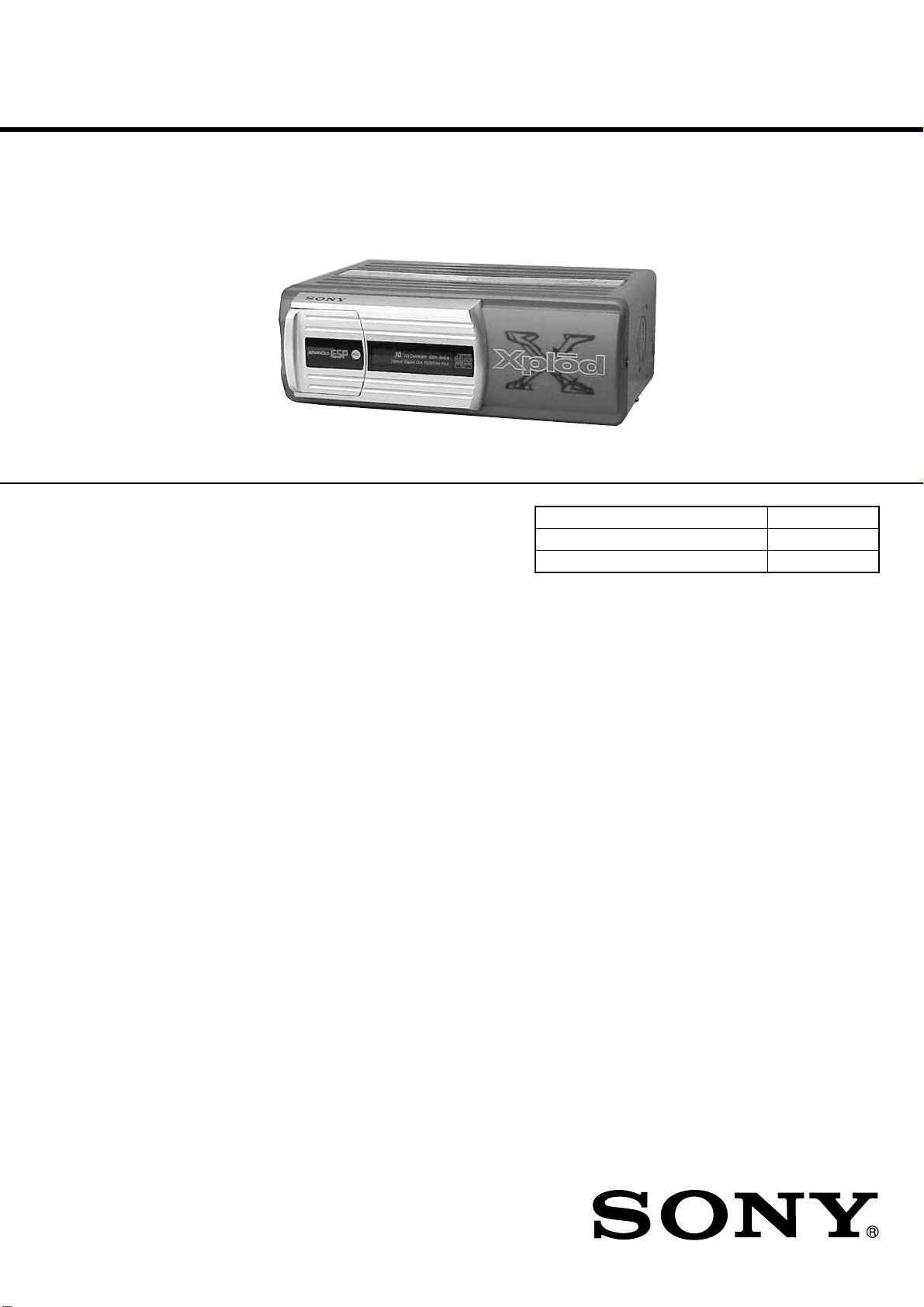
CDX-848X
System Compact disc digital audio system
Laser diode properties Material: GaAlAs
Wavelength: 780 nm
Emission Duration: Continuous
Laser out-put Power: Less than
44.6 µW*
*
This output is the value measured at a distance of 200 mm
from the objective lens surface on the Optical Pick-up Block.
Frequency response 5 – 20,000 Hz
Wow and flutter Below the measurable limit
Signal-to-noise ratio 102 dB
Outputs Optical digital output
BUS control output (8 pins)
Analog audio output (RCA pin)
Current drain 800 mA (during CD playback)
800 mA (during loading or ejecting
a disc)
Operating temperature –10°C to +55°C (14°F to 131°F)
Dimensions Approx. 262 × 90 × 186.5 mm
(10
3
/8 × 3 5/8 × 7
3
/8 in.)
(w/h/d) not incl. projecting parts
and controls
Mass Approx. 2.1 kg (4 lb. 10 oz.)
Power requirement 12 V DC car battery
(negative ground)
Supplied accessories Disc magazine (1)
Parts for installation and
connections (1 set)
Design and specifications are subject to change without
notice.
SERVICE MANUAL
Ver 1.2 2001.06
SPECIFICATIONS
US Model
AEP Model
UK Model
Model Name Using Similar Mechanism NEW
CD Drive Mechanism Type MG-251B-137
Optical Pick-up Name KSS-720A
9-870-244-13 Sony Corporation
2001F0500-1 e Vehicle Company
C 2001.6 Shinagawa Tec Service Manual Production Group
COMPACT DISC CHANGER
Page 2
CDX-848X
L
SERVICING NOTES
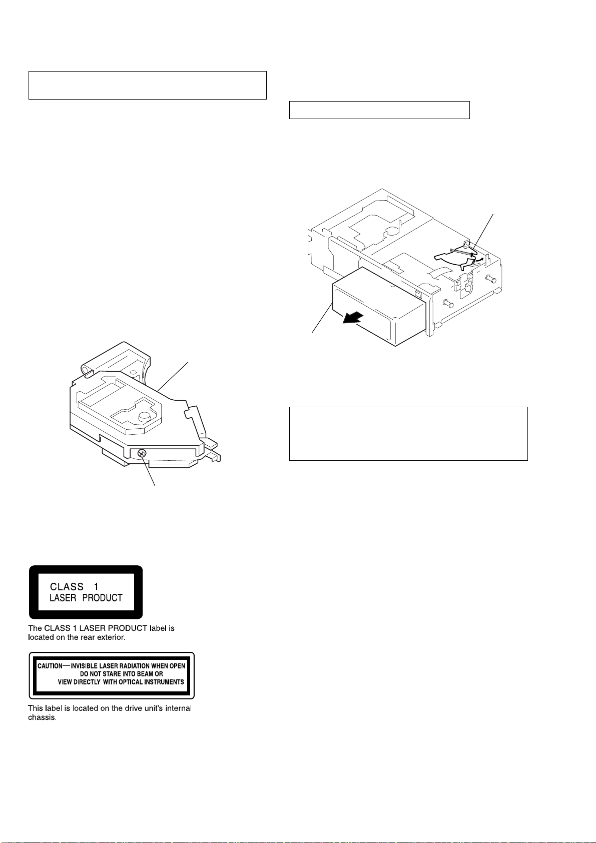
NOTES ON HANDLING THE OPTICAL PICKUP BLOCK OR BASE UNIT
The laser diode in the optical pick-up block may suffer electrostatic breakdown because of the potential difference generated by
the charged electrostatic load, etc. on clothing and the human body .
During repair, pay attention to electrostatic breakdown and also
use the procedure in the printed matter which is included in the
repair parts.
The flexible board is easily damaged and should be handled with
care.
NOTES ON LASER DIODE EMISSION CHECK
The laser beam on this model is concentrated so as to be focused
on the disc reflective surface by the objective lens in the optical
pick-up block. Therefore, when checking the laser diode emission, observe from more than 30 cm away from the objectiv e lens.
US model:
If the optical pick-up block is defective, please replace the whole
optical pick-up block.
Never turn the semi-fixed resistor located at the side of optical
pick-up block.
OPTICA
PICK-UP
BLOCK
DISC MAGAZINE GETTING OUT PROCEDURE
ON THE POWER SUPPLY IS OFF
Remove the CASE (LOWER T) beforehand
1) Press the lever (ML.S) assy in the direction of arrow A.
2) Removal the magazine assy.
Note: Take out the magazine only when the tray is completely within the
magazine. If the disk or tray is sticking out, turn on the power and
eject the magazine.
Lever (ML.S)
A
Magazine assy
AEP/UK model:
CAUTION
Use of controls or adjustments or performance of procedures
other than those specified herein may result in hazardous radiation exposure.
Notes on chip component replacement
• Never reuse a disconnected chip component.
SEMI-FIXED
RESISTOR
• Notice that the minus side of a tantalum capacitor may be damaged by heat.
Flexible Circuit Board Repairing
• Keep the temperature of the soldering iron around 270 ˚C during repairing.
• Do not touch the soldering iron on the same conductor of the
circuit board (within 3 times).
• Be careful not to apply force on the conductor when soldering
or unsoldering.
When replacing the chassis (U.S) sub assy of mechanism deck
which have the “CAUTION LABEL” attached, please be sure to
put a new CA UTION LABEL (3-223-913-11) to the chassis (U.S)
sub assy.
2
SAFETY-RELATED COMPONENT WARNING!!
COMPONENTS IDENTIFIED BY MARK 0 OR DOTTED
LINE WITH MARK 0 ON THE SCHEMATIC DIAGRAMS
AND IN THE PARTS LIST ARE CRITICAL TO SAFE
OPERATION. REPLACE THESE COMPONENTS WITH
SONY PARTS WHOSE PART NUMBERS APPEAR AS
SHOWN IN THIS MANUAL OR IN SUPPLEMENTS PUBLISHED BY SONY.
Page 3
CDX-848X
Ver 1.1 2001.05
NOTE FOR REPLACING IC201
IC201 on MAIN board for this set has been changed in the midway of manufacturing.
In a set that the former type of IC201 is mounted, SUB board is
connected to MAIN board (conductor side).
No service parts are supplied for the former type of IC201 and
SUB board.
When the former type of IC201 is replaced, remove SUB board
and replace the former type of IC201 with the new type.
CHECKING QUALITY OF SUB BOARD
If the set works normally after SUB board is removed from MAIN
board, SUB board has a trouble.
IN this case, remove SUB board and replace IC201 now in use
with the new type of IC201.
Former Type
MAIN
BOARD
IC201
SUB
BOARD
– MAIN BOARD (Component Side) –
MB90473PFV-G-108-
BNDE1
New Type
MB90473PFV-G-110-
BNDE1
TABLE OF CONTENTS
SERVICING NOTES .......................................................... 2
1. GENERAL
Installation....................................................................... 5
Connections ..................................................................... 6
2. DISASSEMBLY
2-1. Disassembly Flow........................................................... 7
2-2. Case (Upper T), Front Panel Assy .................................. 8
2-3. Mechanism Deck (MG-251B-137)................................. 8
2-4. JACK Board, DIGITAL OUT Board.............................. 9
2-5. MAIN Board, Slide Variable Resistor
(Elevator Height Sensor) (RV202) ................................. 9
2-6. ELJ Motor Assy (Elevator) (M104)................................ 10
2-7. Escutcheon (T) ................................................................ 10
2-8. Chassis (U.S) Sub Assy .................................................. 11
2-9. Chassis Assy.................................................................... 11
2-10. RF Board ......................................................................... 12
2-11. Sled Motor Assy (251) (M101),
Optical Pick-up (KSS-720A) .......................................... 12
2-12. LSW Board, Spindle Motor (S) Sub Assy (M102) ........ 13
2-13. ELJ Motor Assy (Chucking) (M103) ............................. 13
3. MECHANISM DECK ASSEMBLY
3-1. Assembly Flow................................................................ 14
3-2. Optical Pick-up Complete Assy...................................... 14
3-3. Gear (Lomini)/(Load Cam) Assy.................................... 15
3-4. Operation Check ............................................................. 15
– MAIN BOARD (Conductor Side) –
SUB BOARD
IC201
4. MECHANICAL ADJUSTMENT.......................... 16
5. ELECTRICAL CHECK .......................................... 17
6. DIAGRAMS
6-1. Block Diagram – SERVO Section – .............................. 19
6-2. Block Diagram – BUS CONTROL/
POWER SUPPLY Section – ........................................... 20
6-3. Note for Printed Wiring Boards and
Schematic Diagrams ....................................................... 21
6-4. Printed Wiring Boards – RF/LSW Boards – ................. 22
6-5. Schematic Diagram – RF/LSW Boards –...................... 23
6-6. Printed Wiring Boards
– MAIN Board (Component Side) – .............................. 24
6-7. Printed Wiring Boards
– MAIN (Conductor Side)/SWITCH Boards –.............. 25
6-8. Schematic Diagram – MAIN Board (1/3) – .................. 26
6-9. Schematic Diagram – MAIN Board (2/3) – .................. 27
6-10. Schematic Diagram
– MAIN (3/3)/SWITCH Boards – ................................. 28
6-11. Printed Wiring Boards
– JACK/DIGITAL OUT Boards – ................................. 29
6-12. Schematic Diagram
– JACK/DIGITAL OUT Boards – .................................. 29
6-13. IC Pin Function Description ........................................... 34
7. EXPLODED VIEWS
7-1. Case Section .................................................................... 37
7-2. Mechanism Deck Section-1 (MG-251B-137) ................ 38
7-3. Mechanism Deck Section-2 (MG-251B-137) ................ 39
7-4. Mechanism Deck Section-3 (MG-251B-137) ................ 40
7-5. Mechanism Deck Section-4 (MG-251B-137) ................ 41
8. ELECTRICAL PARTS LIST ............................... 42
3
Page 4
CDX-848X
SECTION 1
GENERAL
This section is extracted from
instruction manual.
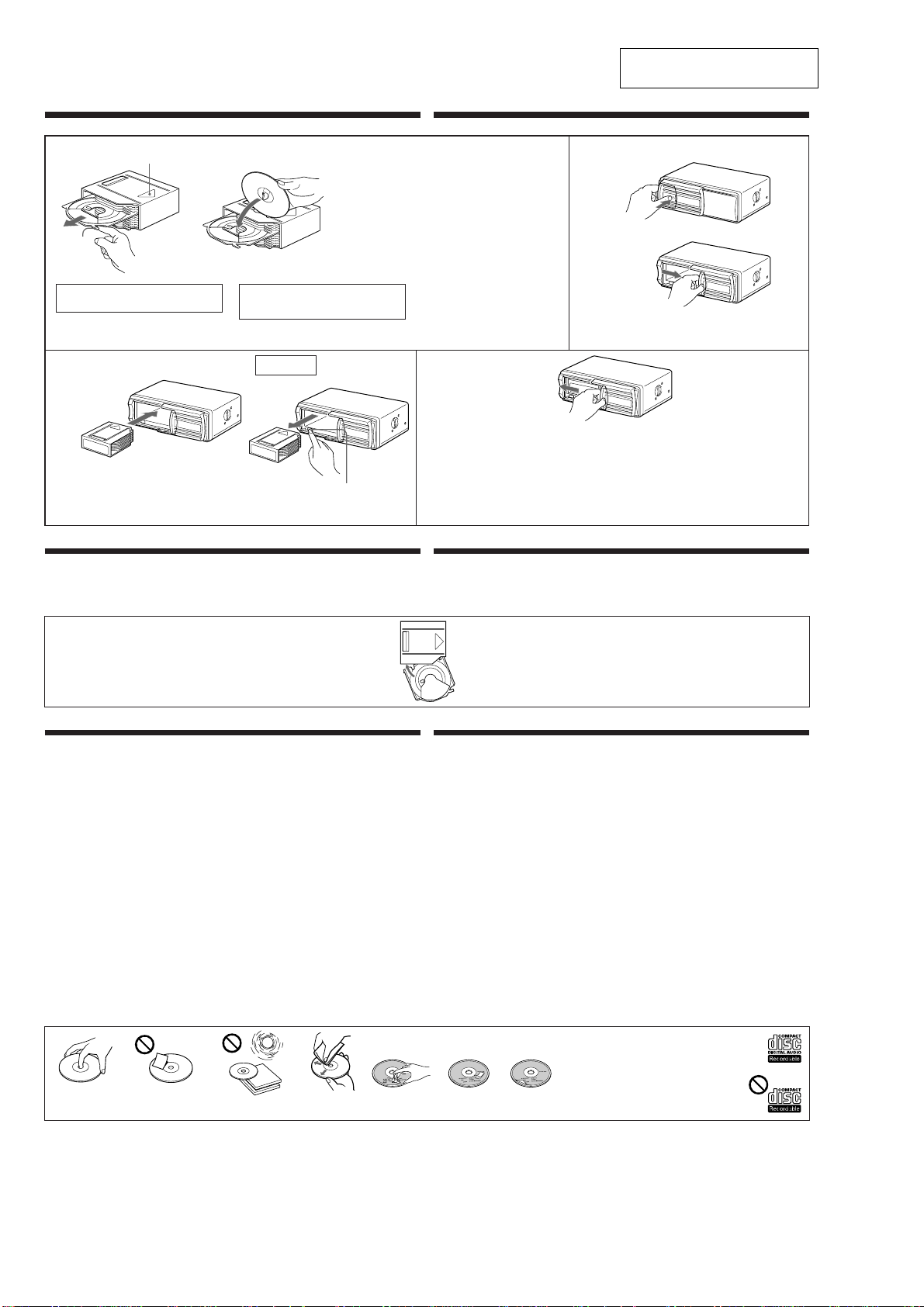
Inserting a disc Insertion d’un disque
With the arrow side facing up
Avec la partie fléchée tournée vers le haut
1
Labeled surface up
Etiquette vers le haut
c
Tab
Onglet
Use the supplied disc magazine or the disc magazine
XA-250.The disc magazine XA-10B can not be used
with this unit.If you use any other magazine,it may
cause a malfunction.
Disc magazine
Chargeur de disques
If the disc magazine does not lock properly
Take out the magazine, and after pressing the Z (EJECT) button,
re-insert it.
Si vous ne pouvez pas fermer le chargeur de disques
Sortez le chargeur et, après avoir appuyé sur la touche Z (EJECT), réinsérez-le.
Notes on the disc magazine
• Do not leave the disc magazine in locations with high temperatures and high humidity such as on a car dashboard or in
the rear window where the disc magazine will be subjected to direct sunlight.
• Do not place more than one disc at a time onto one tray, otherwise the changer and the discs may be damaged.
• Do not drop the disc magazine or subject it to a violent shock.
When the tray comes out
Normally, the trays will not come out of
the magazine. However, if they are
pulled out of the magazine, it is easy to
re-insert them.
With the cut-away portion of the tray facing you,
insert the right corner of the tray in the slot, then
push in the left corner until it clicks.
Note
Do not insert the tray upside down or in the wrong direction.
Utilisez le magasin à disques fourni ou un magasin à
disques XA-250. Vous ne pouvez pas utiliser de
magasin à disques XA-10B avec cet appareil.
L'utilisation d'un autre type de magasin à disques
risque de provoquer un dysfonctionnement.
10 discs, one in each tray
10 disques, un par plateau
To remove
Retrait
Z (EJECT)
Notes
• To listen to an 8 cm (3 in.) CD, use the
separately sold Sony CD adapter CSA-8.
Be sure to always use the specified
adapter, as failing to do so may cause a
malfunction of the unit. If you use any
other adapter, the unit may not operate
properly. When using the Sony CD
adapter, make sure the three catches on
the adapter are firmly latched onto the 8
cm CD.
• Do not insert the Sony CD adapter CSA-8
in the magazine without a disc,
malfunction may result.
Remarques
• Pour écouter un disque de 8 cm (3 po.),
utilisez l’adaptateur Sony CSA-8, vendu
séparément, à l’exclusion de tout autre,
pour éviter tout probléme de
fonctionnement. Si vous utilisez un autre
adaptateur, l’appareil risque de ne pas
fonctionner correctement. Quand vous
utilisez l’adaptateur CD Sony, vérifiez que
les trois griffes soient bien en prise sur le
CD de 8 cm.
• Ne pas insérer d’adaptateur CD Sony CSA8 dans le chargeur sans disque, car cela
pourrait provoquer un
dysfonctionnement.
43
Use the unit with the door closed completely
Otherwise, foreign matter may enter the unit and
contaminate the lenses inside the changer.
Utilisez cet appareil avec la fenêtre complètement
fermée
Sinon, des corps étrangers pourraient pénétrer dans
l’appareil et encrasser les lentilles dans le lecteur.
Remarques sur le chargeur de disques
• Ne pas laisser le chargeur de disques dans un endroit très chaud ou très humide comme sur le tableau de bord ou sur la
plage arrière de la voiture où il serait en plein soleil.
• Ne pas insérer plus d’un disque à la fois sur le plateau, sinon le changeur et les disques risquent d’être endommagés.
• Ne pas laisser tomber le chargeur de disques ni le cogner.
Lorsque le plateau sort
En principe, les plateaux ne sortent pas
du chargeur. Toutefois, s’ils sortent du
chargeur, il est facile de les réinsérer.
Push to unlock the door
Poussez pour déverrouiller la porte
2
Slide open
Coulissez pour ouvrir
Note
To prevent injury, do not insert your hand in the CD changer.
Remarque
Pour éviter toute blessure, ne pas introduire la main dans le changeur de CD.
Note
When a disc magazine is inserted into the CD changer or the
reset button of the connected car audio is pressed, the unit will
automatically be activated and read the information on the
CDs. When the information on all the CDs in the disc magazine
has been read, the unit will automatically stop operation.
Remarque
Quand un chargeur de disques est inséré dans le changeur de
CD ou si la touche de réinitialisation de l’autoradio raccordé est
enclenchée, l’appareil se met automatiquement en marche et
reproduit les CD. Lorsque tous les CD du chargeur ont été
reproduits, l’appareil s’arrête automatiqement.
Avec la portion découpée du plateau vous faisant
face, insérer le coin droit du plateau dans la fente,
puis enfoncer le coin gauche jusqu’au déclic.
Remarque
Ne pas insérer le plateau à l’envers ou dans le mauvais sens.
x
Notes on handling discs
A dirty or defective disc may cause sound drop-outs during playback. To enjoy optimum sound, handle the disc as follows.
• Handle the disc by its edge, and to keep the disc clean, do not touch the unlabeled surface. (fig.
• Do not stick paper or tape on the disc. (fig.
• Keep your discs in their cases or disc magazines when not in use.
Do not expose discs to direct sunlight or heat sources such as hot air-ducts. Do not leave discs in a car parked in
direct sunlight where there can be a considerable rise in the temperature inside the car. (fig.
• Before playing, clean the discs with an optional cleaning cloth. Wipe each disc in the direction of the arrows. (fig.
D
)
Do not use solvents such as benzine, thinner, commercially available cleaners or antistatic spray intended for analog discs.
• Discs with special shapes (heart-shaped discs, octagonal discs etc.) cannot be played on this unit. Attempting to do
so may damage the unit. Do not use such discs.
Notes on discs
If you use the discs explained below, the sticky residue can cause the disc to stop spinning and may cause malfunction or
ruin your discs.
Do not use second-hand or rental CDs that have a sticky residue on the surface (for example from peeled-off stickers or
from ink, or glue leaking from under the stickers).
• There are paste residue. Ink is sticky. (fig.
Do not use rental CDs with old labels that are beginning to peel off.
• Stickers that are beginning to peel away, leaving a sticky residue. (fig.
Do not use your discs with labels or stickers attached.
• Labels are attached. (fig.
Notes on CD-R discs
• You can play CD-Rs (recordable CDs) designed for audio use on this unit (fig. H).
• Some CD-Rs (depending on the equipment used for its recording or the condition of the disc) may not play on this
unit.
• You cannot play a CD-R that is not finalized*.
* A process necessary for a recorded CD-R disc to be played on the audio CD player.
G
)
B
)
E
)
F
)
A
)
C
)
Remarques sur la manipulation des disques
Un disque sale ou défectueux peut provoquer des pertes de son à la lecture. Manipuler le disque comme suit pour obtenir
un son optimal.
• Manipuler le disque par son arête et le maintenir dans un état propre, ne pas le toucher sur la surface non
imprimée. (fig.
• Ne pas coller de papier ou de bande adhésive sur le disque. (fig.
• Conservez vos disques dans leurs boîtiers ou des pochettes de rangement lorsqu’ils ne sont pas utilisés.
Ne pas laisser les disques en plein soleil ou près d’une source de chaleur comme des conduits d’air chaud. Ne pas
laisser les disques dans une voiture garée en plein soleil car la température de l’habitacle risque d’augmenter
considérablement. (fig.
• Avant la lecture, essuyer les disques avec un chiffon de nettoyage en option. Essuyer chaque disque dans le sens
des flèches. (fig.
Ne pas utiliser de solvants tels que de la benzine, du diluant, des produits de nettoyage vendus dans le commerce ou de
vaporisateurs anti-statiques destinés aux disques analogiques.
• Il n’est pas possible d’utiliser les disques de formes spéciales (en forme de cœur ou octogonaux, etc.) avec cet
appareil. Vous risquez d’endommager l’appareil. N’essayez jamais de lire ces disques.
Remarques sur les disques
Si vous utilisez les disques décrits ci-dessous, le résidu adhésif risque de provoquer l’arrêt de la rotation du disque et
d’entraîner un dysfonctionnement ou d’endommager vos disques.
N’utilisez pas de CD de seconde main ou de location qui présentent des résidus adhésifs à la surface (par exemple
d’étiquettes décollées ou d’encre, de colle dépassant de l’étiquette).
• Résidus de colle. L’encre colle. (fig.
N’utilisez pas de CD de location avec d’anciennes étiquettes qui commencent à se décoller.
• Les étiquettes qui commencent à se décoller laissent des résidus adhésifs. (fig.
N’utilisez pas vos disques avec des étiquettes ou des autocollants apposés dessus.
• Les étiquettes sont fixées. (fig.
Remarques sur les disques CD-R
• Vous pouvez écouter avec cet appareil des CD-R (CD enregistrables) conçus pour une utilisation audio. (fig. H)
• Certains CD-R (en fonction des conditions de l’équipement d’enregistrement ou du disque) risquent de ne pas être
lus avec cet appareil.
• Vous ne pouvez pas lire de disques CD-R non finalisés*.
* Un processus nécessaire à la lecture des disques CD-R enregistrés sur le lecteur de CD audio.
A GBCDEF
This way
Oui
Not this way
Non
Not this way
Non
This way
Oui
A
)
C
)
D
)
E
)
G
)
Look for this mark to distinguish CD-Rs for audio use.
H
Ce symbole permet de distinguer les CD-R conçus pour
une utilisation audio.
This mark denotes that a disc is not for audio use.
Ce symbole indique qu’un disque n’est pas conçu
pour une utilisation audio.
B
)
F
)
4
Page 5
CDX-848X
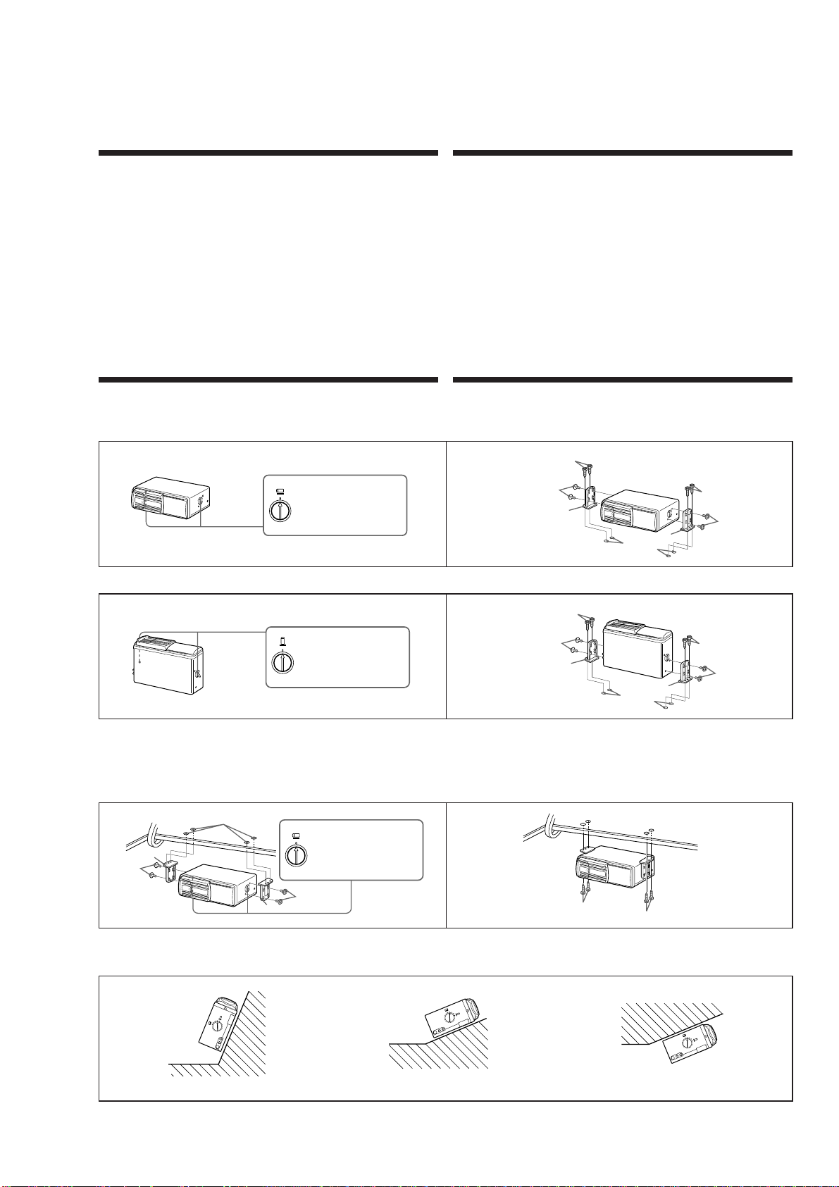
InstallationInstallation
Precautions
• Choose the mounting location carefully, observing the following:
— The unit is not subject to temperatures exceeding 55°C (131°F) (such as in a car parked in direct
sunlight).
— The unit is not subject to direct sunlight.
— The unit is not near heat sources (such as heaters).
— The unit is not exposed to rain or moisture.
— The unit is not exposed to excessive dust or dirt.
— The unit is not subject to excessive vibration.
— The fuel tank should not be damaged by the tapping screws.
— There should be no wire harnesses or pipes under the place where you are going to install the unit.
— The spare tire, tools or other equipment in or under the trunk should not be interfered with or damaged
by the screws or the unit itself.
• Be sure to use only the supplied mounting hardware for a safe and secure installation.
• Use only the supplied screws.
• Make holes of ø 3.5 mm (
surface.
5
/32 in.) only after making sure there is nothing on the other side of the mounting
How to install the unit
The brackets 1 provide two positions for mounting, high and low. Use the appropriate screw holes
according to your preference.
Horizontal installation
1
HORIZONTAL
Align with the marked position.
Aligner sur le repère.
Précautions
• Choisir l’emplacement de montage en tenant compte des observations suivantes:
— Appareil non soumis à des températures dépassant 55°C (131°F) (comme dans une voiture parquée au
soleil).
— Appareil non soumis au rayonnement solaire direct.
— Appareil à l’écart de sources de chaleur (comme des radiateurs).
— Appareil non exposé à la pluie ou à l’humidité.
— Appareil non exposé à des poussières ou à des souillures en excès.
— Appareil non exposé à des vibrations excessives.
— Vérifier que le réservoir d’essence ne risque pas d’être endommagé par les vis taraudeuses.
— Il ne doit pas y avoir de faisceau de fils ou de tuyaux à l’emplacement du montage.
— Vérifier que l’appareil ou les vis ne risquent pas d’endommager ou de gêner la roue de secours, les
outils, ou autre objet dans le coffre.
• Pour garantir la sécurité de l’installation, utiliser uniquement le matériel de montage fourni.
• Utilisez uniquement les vis fournies.
• Ne percez les trous de 3,5 mm (
surface de montage.
5
/32 po.)ø qu'après vous être assuré qu'il n'y avait rien de l'autre côté de la
Installation de l’appareil
Les supports 1 offrent deux positions de montage, haut et bas. Utilisez les trous de vissage appropriés en
fonction de vos préférences.
Installation horizontale
2
Unit: mm (in.)
Unité: mm (po.)
3
2
1
5
/32)
ø 3.5 (
3
2
1
Vertical installation Installation verticale
1
VERTICAL
Align with the marked position.
Aligner sur le repère.
Suspended installation
When the unit is to be installed under the rear tray etc. in the trunk compartment, make sure the following
provisions are made.
• Choose the mounting location carefully so that the unit can be installed horizontally.
• Make sure the unit does not hinder the movement of the torsion bar spring etc. of the trunk lid.
1
1
ø 3.5 (5/32)
HORIZONTAL
Align with the marked position.
Aligner sur le repère.
Unit: mm (in.)
2
Unité: mm (po.)
Installation suspendue
Si l’appareil doit être installé sous la plage arrière dans le coffre, par exemple, observer les précautions
suivantes.
• Bien choisir l’emplacement pour pouvoir installer l’appareil à l’horizontale.
• Vérifier que l’appareil ne gêne pas les mouvements du ressort de fermeture du coffre, entre autres.
2
2
Unit: mm (in.)
Unité: mm (po.)
Inclined installation
After installing the unit, align the dials with one of the marks so that the arrows are as vertical as possible.
2
1
Installation inclinée
Après avoir installé l’appareil, alignez les disques sur un repère de façon à ce que les flèches soient dans la
position la plus verticale possible.
3
2
1
ø 3.5 (5/32)
3
3
3
2
1
V
E
R
T
I
CA
L
L
A
T
N
O
Z
I
R
O
H
Note
Be sure to align the left and right dials with the same mark.
L
A
T
N
O
Z
I
R
O
V
H
E
R
T
I
C
A
L
Remarque
Veillez á aligner les disques gauche et droite sur le même repère.
L
A
T
N
O
Z
I
R
O
V
H
E
R
T
I
C
A
L
5
Page 6
CDX-848X
Connections Conne xions
For details, refer to the Installation/Connections manual of each product. Pour plus de détails, consulter le manuel d’installat ion/connexions de chaque produit.
Schéma de connexionConnection diagram
to a car audio compatible with the Sony BUS optical digital transmission
Sony BUS compatible car audio
Autoradio compatible BUS Sony
system
vers le système audio de la voiture compatible avec le système de
transmission optique numérique BUS Sony
BUS AUDIO IN
Note
For connecting two or more changers, the XA-C30
source selector (optional) is necessary.
Remarque
Pour raccorder deux ou plusieurs changeurs, le
sélecteur de source XA-C30 (en option) est nécessaire.
4
5
Connecting the optional optical
cable
1
After changing the position of the switch, be sure to press the reset button on the main unit.
Notes
•
This switch is factory-set to the ANALOG position.
•
Improper setting of the switch may prevent any sound from being reproduced even when the CD changer is
activated.
2
Set the DIGITAL/ANALOG switch on the side of the CD changer to DIGITAL.
Mettre le commutateur DIGITAL/ANALOG sur le côté du changeur de CD sur
DIGITAL.
Do not touch the coupler parts.
Ne pas toucher les pièces du coupleur.
BUS CONTROL IN
DIGITAL
ANALOG
DIGITAL INBUS CONTROL IN
CDX-848X
Optical cable (optional RC-98, etc.)
Câble optique (RC-98 en option, etc.)
Connexion du câble optique en option
Après avoir modifié la position du commutateur, veiller à appuyer sur la touche de réinitialisation de
l’appareil principal.
Remarques
•
Ce sélecteur est préréglé en usine sur la position ANALOG (analogique).
•
Un réglage incorrect du sélecteur peut empécher la reproduction du son méme quand le changeur de CD
fonctionne.
Optical cable (optional RC-98, etc.)
Câble optique (RC-98 en option, etc.)
Remove the protective cap, and firmly plug in the connector.
3
Notes
•
When you wish to disconnect the cable, simply push in on both sides of the connector.
•
Be sure to keep the protective cap in a safe place for future use.
Notes on the optical cable
Observe the following when connecting the cable:
— Do not bend the cable too much. If the bent part (arc) is less than 10 cm (4 in.) in diameter, sound may not be
reproduced.
— Make sure the cable does not get compressed or constricted in any way by objects around it.
— Never let the coupler parts of the connectors get scratched or become contaminated with dirt.
— If this unit is not connected to a car audio compatible with the Sony BUS optical digital transmission system,
reinstall the protective cap to its original position.
— Use an optical cable designed for Sony car audio systems.
— Not all optical cables can be used with this CD changer.
Retirez le bouchon de protection et enfichez correctement le connecteur.
Protective cap
Cache de protection
6
Protective tubes (to be removed)
Tubes de protection (à enlever)
Remarques
•
Pour débrancher le câble, appuyer simplement sur les deux côtés du connecteur.
•
Garder le capuchon de protection dans un endroit sûr pour une utilisation ultérieure.
Remarques sur le câble optique
Lors de la connexion du câble:
— Ne pas forcer le câble en le pliant. Si la partie courbée (coude) fait moins de 10 cm (4 po.) de diamètre, il est
possible que le son ne soit pas reproduit.
— Vérifier que le câble n’est pas coincé ou écrasé par des objets environnants.
— Protéger les pièces du coupleur des égratignures eet de la saleté.
— Si cet appareil n’est pas raccordé à un autoradio compatible avec le système de transmission numérique optique
BUS Sony digital, réinstaller le capuchon de protection dans sa position d’origine.
— Utilisez un câble optique conçu pour les systèmes audio pour voiture Sony.
— Tous les câbles optiques ne peuvent pas être utilisés avec ce changeur de CD.
Page 7
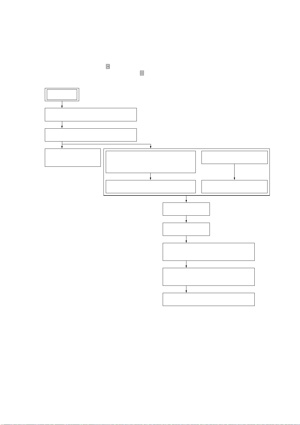
SECTION 2
DISASSEMBLY
• This set can be disassembled in the order shown below.
2-1. DISASSEMBLY FLOW
Note 1: The process described in can be performed in any order.
Note 2: Without completing the process described in , the next process can not be performed.
SET
2-2. CASE (UPPER T), FRONT PANEL ASSY
(Page 8)
2-3. MECHANISM DECK (MG-251B-137)
(Page 8)
CDX-848X
2-4. JACK BOARD,
DIGITAL OUT BOARD
(Page 9)
2-5. MAIN BOARD,
SLIDE VARIABLE RESISTOR
(ELEVATOR HEIGHT SENSOR) (RV202)
(Page 9)
2-6. ELJ MOTOR ASSY (ELEVATOR) (M104)
(Page 10)
2-9. CHASSIS ASSY
(Page 11)
2-10. RF BOARD
(Page 12)
2-11. SLED MOTOR ASSY (251) (M101)
OPTICAL PICK-UP (KSS-720A)
(Page 12)
2-12. LSW BOARD,
SPINDLE MOTOR (S) SUB ASSY (M102)
(Page 13)
2-13. ELJ MOTOR ASSY (CHUCKING) (M103)
(Page 13)
2-7. ESCUTCHEON (T)
(Page 10)
2-8. CHASSIS (U.S) SUB ASSY
(Page 11)
,
7
Page 8
CDX-848X
)
)
)
Note: Follow the disassembly procedure in the numerical order given.
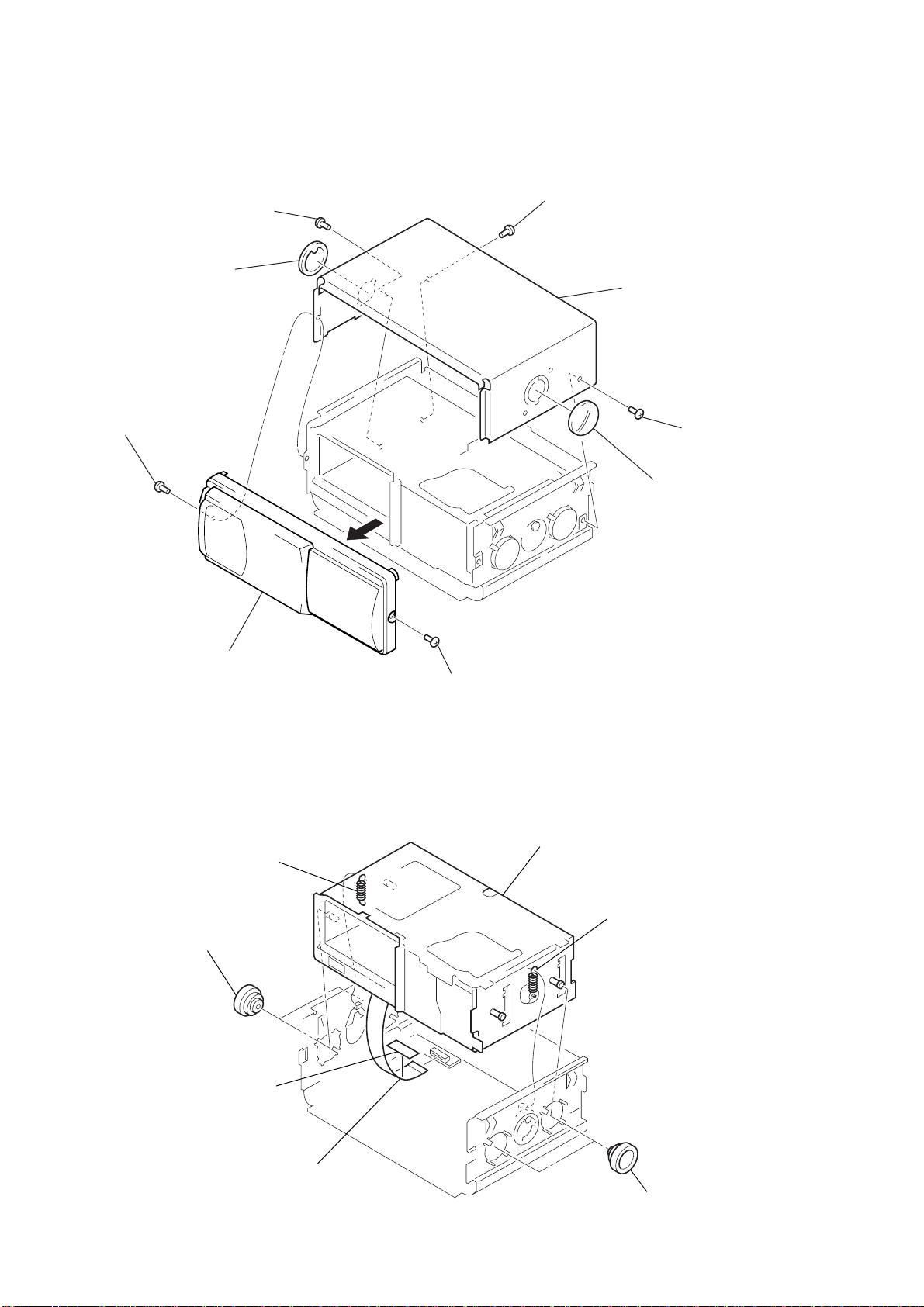
2-2. CASE (UPPER T), FRONT PANEL ASSY
3
screw
1
screw
(PTT2.6
×
6)
4
lever (FLT)
(PTT2.6
×
6)
3
screw (PTT2.6 × 6)
5
case (upper T)
4
lever (FLT)
3
screw (PTT2.6 × 6
2
front panel assy
2-3. MECHANISM DECK (MG-251B-137)
2
tension coil spring (FL)
1
two dampers (T)
filament tape
1
screw (PTT2.6 × 6)
4
mechanism deck (MG-251B-137)
2
tension coil spring (FL
3
jack flexible board
(CNJ901)
1
two dampers (T
8
Page 9
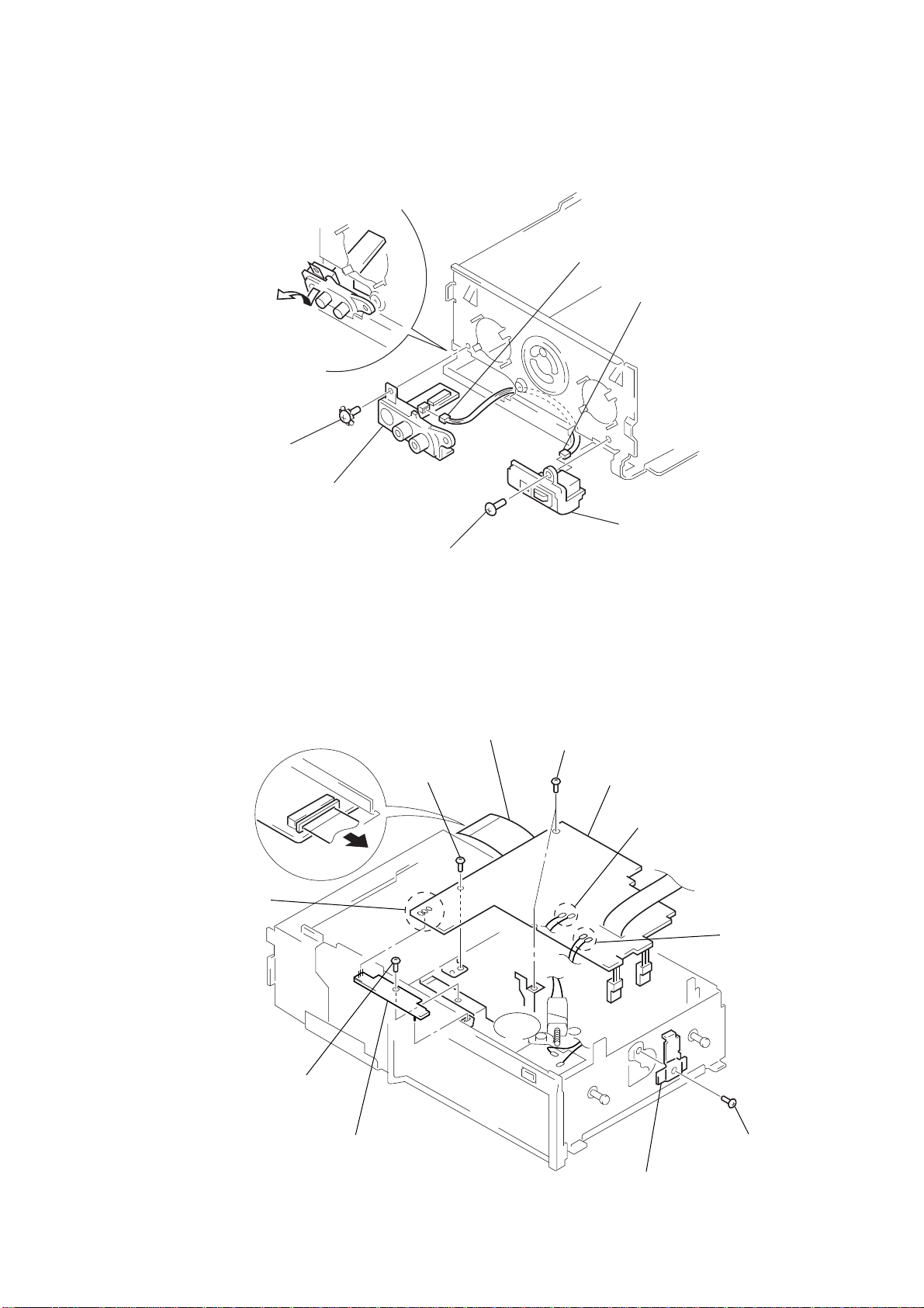
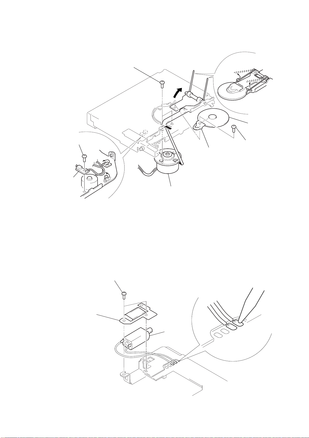
2-4. JACK BOARD, DIGITAL OUT BOARD
d
2
Remove two solders of
the elevator motor leads (M104).
2
Remove two solders of
the switch board leads.
2
Remove three solders of
the slide variable resistor
(RV202).
4
heat sink (T)
3
screw (PTT2 × 4)
6
main board
5
two screws (FP)
1
main flexible board
(CNJ101)
5
screw (FP)
7
screw
(PTT2
×
4)
8
slide variable resistor
(elevator height sensor)
(RV202)
Remove the jack board
in the direction of the arrow.
1
ground point screw
(PTT2.6
×
6)
2
connector
(CN902)
5
connector
(CN701)
CDX-848X
3
jack board
6
digital out boar
4
screw
(BVTT2
×
6)
2-5. MAIN BOARD, SLIDE VARIABLE RESISTOR (ELEVATOR HEIGHT SENSOR) (RV202)
9
Page 10
CDX-848X
)
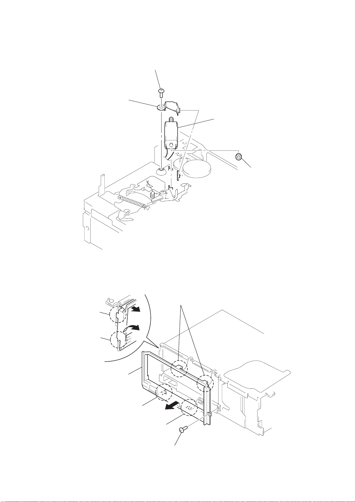
2-6. ELJ MOTOR ASSY (ELEVATOR) (M104)
1
2
bracket (EVM.S)
screw
(PTT2
×
4)
4
ELJ motor assy (elevator) (M104)
3
spacer (MO
2-7. ESCUTCHEON (T)
2
Remove the claw
in the direction of arrow
4
Remove the ditch
in the direction of arrow
5
Remove the escutcheon (T)
in the direction of arrow
A
B
two claws
3
.
.
C
.
3
claw
B
A
4
C
ditch
1
screw (T)
10
Page 11
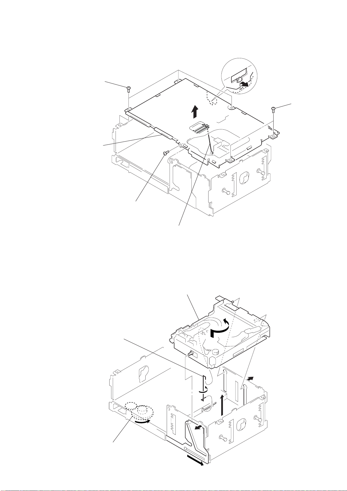
2-8. CHASSIS (U.S) SUB ASSY
1
three screws
(PTT2 × 4)
5
chassis (U.S) sub assy
3
A
2
Remove the edge
in the direction
of arrow A.
CDX-848X
1
two screws
(PTT2 × 4)
2-9. CHASSIS ASSY
5
1
screw
(PTT2 × 4)
spring (stopper.lower)
4
spring (SUT)
6
chassis assy
4
1
Turn the gear (EVD.S) fully
in the direction of arrow A.
3
2
A
3
11
Page 12
CDX-848X
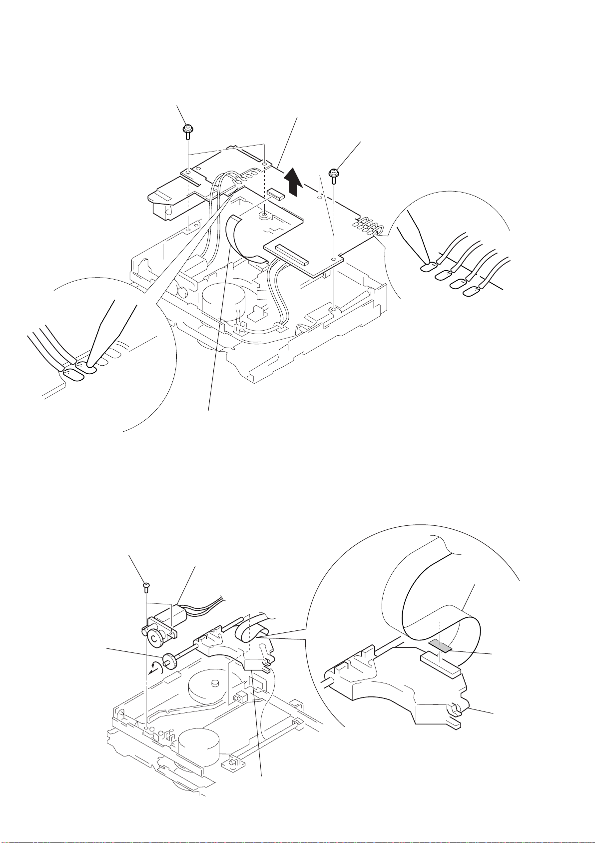
2-10. RF BOARD
3
two screws
(PTT2
×
4)
4
RF board
3
two screws
×
4)
(PS2
2
Remove four solders
of the LSW board leads
and spindle motor leads (M102).
2
Remove two solders
of the sled motor leads
(M101).
1
OP flexible board (CN102).
2-11. SLED MOTOR ASSY (251) (M101), OPTICAL PICK-UP (KSS-720A)
1
two precision screws
4
Turn shaft (feed) assy
in the direction
of the arrow,
then remove it.
(P2 × 3)
2
sled motor assy (251)
(M101)
OP flexible board
adhesive
sheet
12
3
optical pick-up
(KSS-720A)
optical
pick-up
Note: After connecting OP flexible board,
fix it with adhesive sheet
to optical pick-up.
Page 13
2-12. LSW BOARD, SPINDLE MOTOR (S) SUB ASSY (M102)
)
w
8
two precision screws
(P1.7
×
2.2)
7
1
precision screw
(P2
×
2.5)
5
bracket (CP)
CDX-848X
spring (chucking)
3
6
retainer (disc
4
precision scre
(P2 × 2.2)
2
LSW board
2-13. ELJ MOTOR ASSY (CHUCKING) (M103)
2
two screws
(PTT2 × 4)
3
retainer (CHM)
9
Remove the spindle motor (S) sub assy (M102)
in the direction of the arrow.
1
Remove two solders of
the chucking motor leads (M103).
4
ELJ motor assy (chucking) (M103)
13
Page 14
CDX-848X
)
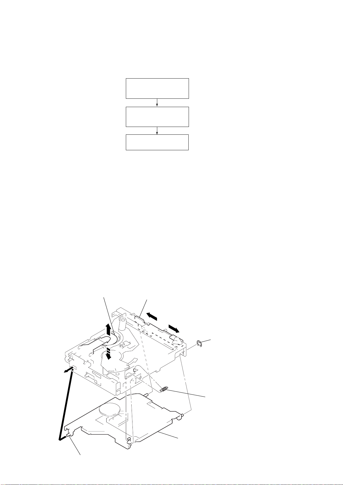
MECHANISM DECK ASSEMBLY
• This set can be disassembled in the order shown below.
3-1. ASSEMBLY FLOW
SECTION 3
3-2. OPTICAL PICK-UP
COMPLETE ASSY
(Page 14)
3-3. GEAR (LOMINI)/
(LOAD CAM) ASSY
(Page 15)
3-4. OPERATION CHECK
(Page 15)
3-2. OPTICAL PICK-UP COMPLETE ASSY
1
Move the lever (LOCK 3A) in the direction of arrow A,
and return it a little in the direction of arrow
chuck plate
from the position where the chuck plate is moved
down to the lower limit.
B
A
B
stop ring 2.0 (E type
3
4
tension spring (DH)
14
shaft (A)
2
optical pick-up complete assy
Note: Insert the shaft (A) first.
Page 15

3-3. GEAR (LOMINI)/(LOAD CAM) ASSY
CDX-848X
gear (LOAD 2)
marking
Fig. A
3
Attach the gear (LOAD CAM) assy
with its facing inside.
gear (LOMINI)
slit
chuck plate
2
Attach the gear (LOMINI) at the position
shown in Fig. A.
shaft (rotary prevention C)
1
B
stop ring 1.5 (E type)
4
Move the lever (LOCK 3A)
fully in the direction of arrow
to move the chuck plate up.
B
3-4. OPERATION CHECK
1
Confirm that the slider moves in the direction of arrow C to move down
the chuck plate if the gear (LOAD CAM) is rotated in the direction of arrow
A
or the chuck plate moves up and the slider moves in the direction of
arrow D if the gear is rotated in the direction of arrow B.
chuck plate
slider
D
C
A
gear (LOAD CAM) assy
B
15
Page 16
CDX-848X
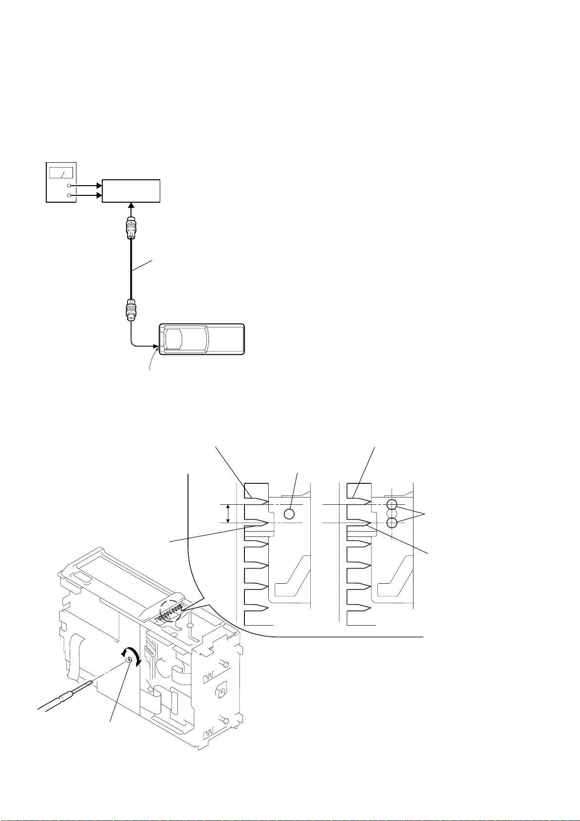
MECHANICAL ADJUSTMENT
• Elevator Height (Address) Adjustment
SECTION 4
Note: This adjustments is necessary when the system controller (IC201),
variable resistor (RV201), slider (R), slider (L), or chassis (ELV)
was replaced for any repair.
Connection:
power supply
(DC 14.4 V)
master unit
+
GND
BUS cable
compact disc changer
CONTROL connector
(CN901)
Adjustment Method:
1. Connect this set to the master unit (e.g. MDX-C7970/C7970R),
load a disc magazine, and place the set vertically as shown
below.
2. Connect the regulated power supply to the master unit, and
turn the power on.
3. Press the DISC button on the master unit and select DISC 5.
4. At this time, if the elevator shaft does not position between
comb teeth A and B at addresses 5 and 6 as shown below,
adjust the following.
5. Press repeatedly the DISC + and – buttons on the master unit
so that the elevator shafts moves from address 6 to address 5,
or from 5 to 6. At this time, adjust RV201 on the main board
so that the elevator shaft positions smoothly between comb
teeth A and B.
6. Further, place the set horizontally and make same adjustment
as mentioned above.
7. After adjustment at addresses 5 to 6 is finished, check all operations from addresses 1 to 10 with the set placed vertically
and horizontally respectively to confirm that the ele vator shaft
positions in a range between comb teeth A to B.
comb tooth at address 6
comb tooth at address 5
comb tooth at address 6
elevator shaft
A
B
OK NG
A
elevator shaft
B
comb tooth at address 5
16
RV201
Page 17

SECTION 5
ELECTRICAL CHECK
CDX-848X
Note:
1. This check is performed with the set placed horizontally.
2. Power supply voltage: DC14.4 V (more than 3 A).
3. Be sure to use the disc “YEDS-18” parts code: 3-702-101-01, but only
when indicated.
Connection:
power supply
(DC 14.4 V)
master unit
+
GND
BUS cable
Focus Bias Check
Connection:
– RF Board (Component Side) –
oscilloscope
(AC range)
+
–
TP (RFAC)
TP (VC)
IC101
compact disc changer
CONTROL connector
(CN901)
Procedure:
1. Connect the oscilloscope to TP (RFAC) and TP (VC) on the
RF board.
2. Put the set into play mode by loading the disc (YEDS-18).
3. Confirm that oscilloscope waveform is clear and check RF signal level is correct or not.
Note:
Clear RF signal waveform means that the shape “◊” can be clearly distinguished at the center of the waveform.
RF signal waveform
VOLT/DIV: 200 mV
TIME/DIV: 500 ns
(10 : 1 probe in use)
level: 1.4 ± 0.3 Vp-p
When observing the eye pattern, set the oscilloscope to AC range
and raise the vertical sensitivity so that it may be easily seen.
17
Page 18

CDX-848X
Tracking Offset Check
Connection:
– RF Board (Component Side) –
oscilloscope
(DC range)
+
–
TP (VC)
IC101
TP (TE)
Procedure:
1. Connect the oscilloscope to TP (TE) and TP (VC) on the RF
board.
2. Put the set into play mode by loading the disc (YEDS-18).
. >
3. Press the
[ AMS ] button on the master unit, and check
the traverse waveform*.
4. Confirm that the oscilloscope waveform is symmetrical on the
top and bottom in relation to 0 V dc, and check this level.
* Traverse waveform: This is the tracking error wave form appears
when crossing the track.
Traverse waveform
A
0 V
B
VOLT/DIV: 500 mV
TIME/DIV: 2 ms
Center: 0 V
18
A=B
traverse waveform
(100 track jump waveform)
Page 19

6-1. BLOCK DIAGRAM – SERVO Section –
CDX-848X
SECTION 6
DIAGRAMS
DETECTOR
A
B
C
D
E
F
LASER DIODE
OPTICAL
PICK-UP BLOCK
(KSS-720A)
(TRACKING)
(FOCUS)
I-V AMP
PD LD
2-AXIS DEVICE
A
6
B
7
C
8
D
9
E
10
F
11
AUTOMATIC
CONTROL
M101
(SLED)
M102
(SPINDLE)
M103
(CHUHCKING)
RF AMP,
FOCUS/TRACKING ERROR AMP
POWER
Q101
IC101
RFAC
SUMMING
AMP
RFDC
SUMMING
AMP
FOCUS
ERROR
AMP
TRACKING
ERROR
AMP
LD
1
TRACKING/FOCUS COIL DRIVE,
SLED/SPINDLE/CHUCKING
VO3 +
8
VO3 –
9
VO4 +
6
VO4 –
7
VO2 +
10
MM
MM
MM
VO2 –
11
VO1 +
12
VO1 –
13
VL0 +
5
VL0 –
4
SUM
RW/ROM
APC AMP
MOTOR DRIVE
AC
RW/ROM
IC201
MOTOR
COIL
DRIVE
DRIVE
COIL
DRIVE
MOTOR
DRIVE
MOTOR
DRIVE
MOTOR
DRIVE
4 3
DC OFST
SW
PD
VIN3 +
VIN3 –
VIN4 +
VIN4 –
VIN2 +
VIN2 –
VIN1-B
FWD
RFDCO
12
2
REV
EQ IN
FE
TE
25
24
31
32
22
21
18
1
2
RFAC
VCA
RF
28
30
FE
16
TE
18
RF EQ
AMP
RF AMP OFFSET
CONTROL SWITCH
Q102
TFDR
48
TRDR
49
FFDR
50
FRDR
51
SFDR
46
SRDR
47
MDP
43
RFAC
15
D-RAM
IC102
RF
RFDC
ANALOG SW
A/D CONVERTER
SERVO DSP
PWM GENERATOR
DIGITAL
CLV
71
73
74
DQ1 – DQ4
A0 – A10
RAS
CAS
WE
OE
FE
TE
FE
TE
OP AMP
RFAC
ASYMMETRY
CORRECTOR
ASYI
ASYO
2, 3,
24, 25
21, 8
9 – 12, 15 – 19,
5
23
4
22
61606258
SE
MIRR
DECT
FOK
FILTER
66 69 68 67
FILI
PCO
FILO
CLTV
DIGITAL
PLL
D0 – D3
118, 117
116, 115,
A0 – A10
3 – 1, 111
109 – 106, 7 – 5,
XRAS
113
XCAS
119
XWE
114
XOE
120
ON : When completion of the disc
ON : When completion of the disc
chucking operation
chucking operation
ON : When completion of the disc
ON : When completion of the disc
save operation
save operation
VIBRATION
MEMORY
CONTROLLER
&
COMPRESSION
EXPANDER
XRDE
XWRE
XQOK
ON : When the optical pick-up
ON : When the optical pick-up
is inner position
is inner position
DIGITAL SIGNAL PROCESSOR,
DIGITAL SERVO PROCESSOR,
D-RAM CONTROLLER
IC101
EFM
DEMODULATOR
INTERNAL BUS
SUBCODE
PROCESSOR
SW3
(LIMIT)
SW1
(CHUCKING END DETECT)
SW2
(SAVE END DETECT)
D/A
INTERFACE
32k RAM
ERROR
CORRECTOR
CPU
INTERFACE
SERVO AUTO
SEQUENSOR
SERVO
INTERFACE
SSTP
45
WDCK
GFS
DATA
CLOK
XLAT
SENS
SQSO
SQCK
SCOR
XRDE
XWRE
XQOK
SCLK
FOK
XRST
1578
1581
1523
1525
1524
1526
1514
1515
1517
159
158
1512
27
35
21
DIGITAL
OUT
SELECTOR
CLOCK
GENERATOR
DOUT
PCMD
BCK
LRCK
XTAI
XTAO
1585
15
88
1588
15
90
15
86
1593
1594
DATA
2
BCK
3
LRCK
1
CD-ROM/RW
SELECT SWITCH
Q202
SERIAL
INPUT
INTERFACE
INTERFACE
MODE
CONTROL
DM1
8 TIME OVER
SAMPLING
DIGITAL FILTER
WITH
FUNCTION
CONTROLLER
RST
2227
66
99
53
42
61
59
60
44
56
58
52
64
65
63
43
41
62
5
6
98
97
96
MULTI LEVEL
∆ ∑
MODULATOR
BPZ
CONTROL
DIGITAL FILTER,
D/A CONVERTER
IC501
EMPH
RW SEL
GRSCOR
GFS
CDDAT
CDCLK
CDLAT
SENS
SQSO
SQCK
SCOR
XRDE
XWRE
XQOK
SYSTEM CONTROLLER
SCLK
FOK
XRST
LOADF
LOADR
LIM SW
LOAD SW
SAVE SW
DOUTSEL
IC201 (1/2)
D/A
CONVERTER
CLKO
67MUTEMUTE
90
LOW-PASS
FILTER
CRYSTAL
OSCILLATOR
XTI
XTO
3 64
X501
16.9344MHz
SW701
ANALOG
DIGITAL
VOUTL
1516
VOUTR
1513
SCK
MUTING CONTROL
SWITCH
Q402
• SIGNAL PATH
: CD PLAY (ANALOG OUT)
: CD PLAY (DIGITAL OUT)
LOW-PASS
LOW-PASS
FILTER
FILTER
IC401
IC401
MUTING
Q410, 420
OPTICAL
TRANSEIVER
IC701
LINE
AMP
IC402
IC701
DIGITAL OUT
L
R
CN901 (1/2)
ANALOG OUT
1919
Page 20

CDX-848X
6-2. BLOCK DIAGRAM – BUS CONTROL/POWER SUPPLY Section –
SYSTEM CONTROLLER
ON : When magazine
is set
SW201
MAGAZINE
DETECT
51
MAGLK SW
IC201 (2/2)
MCK
37
RV201
ELEVATOR HEIGHT
(ADDRESS)
M104
(ELEVATOR)
ELEVATOR
MOTOR DRIVE
IC301
OUT1
9
M
OUT2
7
MOTOR
DRIVE
IN1
IN2
EEPROM
IC203
SDA
SCL
ELVF
3
4
5
6
4
3
ELVR
EEDAT
32
28
EECLK
EHS
AVRH
ELVON
BUCHK
EJECT SW
CDON
RESET
36
34
24
46
50
23
75
RV202
ELEVATOR HEIGHT
SENSOR
BATTERY
CHECK
Q301
SW801
Z
RESET SIGNAL
GENERATOR
IC303
D306
SERVO +3.3V
BUS INTERFACE
(FOR SONY BUS)
IC302
B. UP +3.3V
DRIVER +8V
D307
+3.3V
REGULATOR
IC306
DAC/SERVO +5V
14
VCC
+8V
REGULATOR
IC304
+5V
REGULATOR
IC305
+3.3V
REGULATOR
Q303, 304
PS901
CN901 (2/2)
CONTROL
7
B. UP
X180X0
81
X201
4MHz
UNI SI
UNI SO
UNI CK
BUSON
SO
16
17
18
45
10 6
SI
9
SCK
11 4
BUSON OUT
1 12
BUSON OUT
13 2
RESET
8 7
RESET
SWITCH
DATA
CLK
LOF
BUSON IN
RST
5
DATA
4
CLK
6
BUSON
2
RST
2020
Page 21

CDX-848X
d
6-3. NOTE FOR PRINTED WIRING BOARDS AND SCHEMATIC DIAGRAMS
Note on Printed Wiring Board:
• X : parts extracted from the component side.
• Y : parts extracted from the conductor side.
f
•
• : Pattern from the side which enables seeing.
(The other layers' patterns are not indicated.)
Caution:
Pattern face side: Parts on the pattern face side seen from
(Conductor Side) the pattern face are indicated.
Parts face side: Parts on the par ts face side seen from
(Component Side) the parts face are indicated.
: internal component.
Note on Schematic Diagram:
• All capacitors are in µF unless otherwise noted. pF: µµF
50 WV or less are not indicated except for electrolytics
and tantalums.
• All resistors are in Ω and 1/
specified.
f
•
• C : panel designation.
Note: The components identified by mark 0 or dotted line
• A : B+ Line.
• H : adjustment for repair.
• Po wer voltage is dc 14.4V and fed with regulated dc pow er
• Voltages and waveforms are dc with respect to ground
• V oltages are taken with a VOM (Input impedance 10 MΩ).
• Waveforms are taken with a oscilloscope.
• Circled numbers refer to waveforms.
• Signal path.
: internal component.
with mark 0 are critical for safety.
Replace only with part number specified.
supply from CD changer controller.
under no-signal conditions.
no mark : CD PLAY
Voltage variations may be noted due to normal production tolerances.
Voltage variations may be noted due to normal production tolerances.
J : CD PLAY (ANALOG OUT)
c : CD PLAY (DIGITAL OUT)
: Impossible to measure
∗
4
W or less unless otherwise
• Circuit Boards Location
JACK board
MAIN board
DIGITAL OUT board
SWITCH board
RF boar
LSW board
2121
Page 22

CDX-848X
6-4. PRINTED WIRING BOARDS – RF/LSW Boards – • See page 21 for Circuit Boards Location.
• Semiconductor
Location
Ref. No. Location
IC101 H-6
IC201 J-5
Q101 F-7
Q102 H-7
1
2 3 4 5 6 7 8 9 10 11 12 13
A
SW2
B
SW1
CHUKING
END DETECT
SAVE END
DETECT
C
TP106
TP105
TP103
TP104
WHT
YEL
RED
BLK
D
M101
M
(SLED)
E
M103
M
(CHUKING)
F
G
OPTICAL
PICK-UP
BLOCK
(KSS-720A)
OP FLEXIBLE
BOARD
CN102
R103
H
C107
TP
TP
(VC)
(RFAC)
R223
R222
R104
R220
R218
R219
C202
IC201
C106
R106
C209
R215
SW3
MAIN FLEXIBLE
1-679-422-
BOARD
11
(11)
CNJ101
R214
R212
R210
R208
R206
R204
R201
R213
R211
R209
R207
R205
R203
R202
C208
C207
C206
C205
C204
C203
C217
I
A
MAIN BOARD
(Page 24)
J
LSW BOARD
BLU
K
(LIMIT)
YEL
R102
IC101
TP
(TE)
R107
C109
R108
R216
R109
C103
C111
R110
Q101
C101
R117
C102
R119
R105
R122
R113
TP107
TP108
TP102
TP101
R101
Q102
R121
C108
R120
R112
1-679-421-
C104
C122
YEL
BLU
BLK
RED
(11)
C121
M102
M
(SPINDLE)
11
C105
C201
1-679-421-
11
(11)
2222
Page 23

6-5. SCHEMATIC DIAGRAM – RF/LSW Boards – • See page 30 for for Waveforms. • See page 30 for IC Block Diagrams.
CDX-848X
(Page 26)
The components identified by mark 0 or dotted
line with mark 0 are critical for safety.
2323
Replace only with part number specified.
Page 24

CDX-848X
Ver 1.1 2001.05
• Semiconductor
Location
Ref. No. Location
D302 D-3
D303 E-3
D306 F-6
D307 F-5
D310 G-4
D313 E-3
D314 D-3
IC101 C-9
IC102 D-7
IC201 F-9
IC203 H-10
IC301 H-4
IC302 D-3
IC303 G-3
IC306 A-9
IC401 D-6
IC402 D-5
IC501 B-7
Q202 G-11
Q301 F-6
Q303 F-4
Q304 G-4
Q402 E-4
Q410 D-4
Q420 E-4
6-6. PRINTED WIRING BOARDS – MAIN Board (Component Side) – • See page 21 for Circuit Boards Location.
1
2 3 4 5 6 7 8 9 10 11 12
A
C307
R303
C162
C501
C502
IC501
C506
C504
FB101
R501
C112
C113
C161
IC102
C203
R205
R206
R208
B
R401
D307
R408
R407
Q301
C406
R406
C404
D306
C403
R405
C405
R403
IC401
R402
R404
R302
C
C304
C317
D314
D302
C305
D
C318
IC302
C306
D313
R301
D303
Q410
Q420
R416
R415
C412
C411
IC402
R414
R413
E
CN301
F
G
C309
IC303
D310
C308
R305
R311
R306
R310
C312
Q402
Q303
Q304
R411
R409
C408
R410
R412
R304
IC301
C302
H
C314
C301
C303
SW201
MAGAZINE
DETECT
R204
C110
C109
C111
R106
R207
C205
R107
R105
IC101
C106
C104
C108
C107
C114
IC201
IC306
R103
C115
C105
R102
R104
C202
R109
R122
C122
R108
R123
C123
R125
C121
R101
C103
C102
C101
R201
C201
R202
C204
R222
R211
R210
R203
R250
C206
R221
Q202
R209
A
RF BOARD
CNJ101
(Page 22)
MAIN FLEXIBLE BOARD
IC203
JACK FLEXIBLE BOARD
Y
B
I
JACK BOARD
CNJ901
SUB BOARD
(Page 25) (Page 25)
X
SUB BOARD
(Page 29)
J
K
11
1-679-417-
(11)
2424
Page 25

6-7. PRINTED WIRING BOARDS – MAIN (Conductor Side)/SWITCH Boards – • See page 21 for Circuit Boards Location.
1
2 3 4 5 6 7 8 9 10 11
A
BP201
X501
X201
C505
BP302
(CHASSIS)
C503
C508
BP301
BLK
RED
C407
C410
C409
C311
YEL
BLU
C509
M
M104
(EVEVATOR)
B
(CHASSIS)
C319
C
D
RV201
E
F
G
H
(CHASSIS)
I
BP121
BP122
CDX-848X
Ver 1.1 2001.05
• Semiconductor
Location
Ref. No. Location
IC304 H-11
IC305 F-11
C316
IC305
C313
C310
C315
IC304
1-679-417-
11
(11)
J
SWITCH BOARD
YEL
BLU
RV202
EVEVATOR
HEIGHT
K
SENSOR
SW801
Z
SUB BOARD
TP6
TP5
TP4
TP3
TP2
TP1
X
(COMPONENT SIDE)
(COMPONENT SIDE)
Y
(Page 24)
MAIN BOARD
MAIN BOARD
(Page 24)
(NOT SUPPLIED: See page 3)
(CHASSIS)
2525
Page 26

CDX-848X
6-8. SCHEMATIC DIAGRAM – MAIN Board (1/3) – • See page 30 for Waveforms. • See page 30 for IC Block Diagrams.
(Page 23)
(Page 27)
(Page 28)
2626
Page 27

6-9. SCHEMATIC DIAGRAM – MAIN Board (2/3) – • See page 30 for Waveform. • See page 30 for IC Block Diagram.
(Page 26)
SUB
BOARD
TP6
(Page 26)
CDX-848X
Ver 1.1 2001.05
(Page 28)
2727
Page 28

CDX-848X
Ver 1.1 2001.05
6-10. SCHEMATIC DIAGRAM – MAIN (3/3)/SWITCH Boards – • See page 30 for Waveforms. • See page 30 for IC Block Diagrams.
(Page
26)
(Page
27)
(Page 29)
(Page 27)
SUB BOARD
(NOT SUPPLIED: See page 3)
2828
Page 29

6-11. PRINTED WIRING BOARDS – JACK/DIGITAL OUT Boards –
• See page 21 for Circuit Boards Location.
C902
C901
PS901
D901
D902
C904
CN902
CNJ901
6-12. SCHEMATIC DIAGRAM – JACK/DIGITAL OUT Boards –
CDX-848X
1-679-418-
FB902
FB903
FB901
(11)
JACK FLEXIBLE
BOARD
B
MAIN BOARD
CN301
(Page 24)
(Page 28)
CN701
C701
R701
11
11
1-679-420-
(11)
ANALOG OUT
CONTROL
(FOR SONY BUS)
5 4
6
7
8
2 13
IC701
DIGITAL
OUT
CN901
L
R
7
8
4
5
1
2
3
6
1
2
3
4
SW701
DIGITAL
ANALOG
1-679-420-
11
(11)
2929
Page 30

CDX-848X
• Waveforms
– RF Board –
1 IC101 qh (FE) (CD play mode)
Approx.
100 mVp-p
2 IC101 qk (TE) (CD play mode) 2
Approx.
250 mVp-p
3 IC101 qg (RFAC) (CD play mode)
– MAIN Board –
1 IC101 rd (MDP) (CD play mode) 5 IC201 ia (X1) (CD play mode)
3
3.8 µs
IC101 ih (LRCK), IC501 1 (LRCK)
(CD play mode)
22.7 µs
IC101 o; (BCK), IC501 3 (BCK)
(CD play mode)
2 Vp-p
4.5 Vp-p
250 ns
6 IC501 6 (XTO) (CD play mode)
59.1 ns
3.9 Vp-p
6.2 Vp-p
• IC Block Diagrams
–RF Board –
IC101 CXA2581N-T4
APC AMP
A
B
C
D
VC
A
–
+
RFAC
SUMMING
AMP
BCD
EQ IN
AC SUM
GND
DVC
VC
1
LD
2
PD
3
4
5
6
A
7
B
8
C
9
D
VOFST
RW/ROM
30
DC OFST
29
A
B
C
D
B
C
A
D
DVC
RW/ROM
EQ ON/OFF
RW/ROM
RW/ROM
RW/ROM
–
+
VOFST
–
+
–
+
DVC
VCC
EQ
RFAC
VCA
VCC
–
+
DVC
VC
RFDCI
28
RFDCO
VC
27
VC
26
RFC
25
VFC
24
BST
23
RFG
22
VCC
21
CEI
20
CE
19
TE BAL
1.4 ± 0.3 Vp-p
472 ns
4
IC101 od (XTAI), IC501 4 (CLKO)
(CD play mode)
59.1 ns
4.7 Vp-p
5.4 Vp-p
SW
DVCC
DVC
RFAC
10
E
11
F
12
13
DVC
14
15
GM
GM
APC-OFF
(Hi-Z)
RW/ROM
(H/L)
–
+
VC
RW/ROM
RW/ROM
B
D
A
C
VOFST
–
+
RW/ROM
–
+
DVC
VC
18
TE
17
FEI
16
FE
3030
Page 31

IC201 LA6576L-TE-L
FWD
1
INPUT
2
REV
3
VCC2
4
VLO–
5
VLO+
6
VO4+
7
VO4–
8
VO3+
9
VO3–
10
VO2+
VO2–
11
12
VO1+
VO1–
13
VCC1
14
15
VIN1
OUTPUT
CONTROL
LEVEL
SHIFT
LEVEL
SHIFT
–
+
LEVEL
SHIFT
LEVEL
SHIFT
–
+
THERMAL SHUT DOWN
–
+
5VREG
+
–
–
+
–
+
CH2-4
MUTE
CH1
MUTE
VIN1/VREF
SWITCH
–
+
–
+
+
–
+
–
S-GND
36
35
MUTE2
34
MUTE1
33
VIN4
32
VIN4–
31
VIN4+
30
VREF-IN
29
VIN1 (VREF)-SW
28
VREF-OUT (CH1)
27
REG-OUT
REG-IN
26
25
VIN3+
VIN3–
24
VIN3
23
22
VIN2+
21
VIN2–
VIN2
20
VIN1+B
19
CDX-848X
16
VIN1–A
VIN1+A
VIN1–B
–
AMP-A
+
17
–
18
AMP-B
+
–MAIN Board –
IC102 MSM51V17400D-10TK-FS
COLUMN
ROW
TIMING
GENERATOR
INTERNAL
ADDRESS
COUNTER
ROW
DECODERS
REFRESH
CONTROL
CLOCK
WORD
DRIVERS
COLUMN
DECODERS
SENSE
AMPLIFIERS
MEMORY
CELLS
TIMING
GENERATOR
I/O
SELECTOR
INPUT
BUFFERS
DATA BUS
WRITE
CLOCK
GENERATOR
OUTPUT
BUFFERS
1 26
VCC
DQ1
2
3
DQ2
4
WE
5
RAS
NC
6
7
NC
8
A10
9
A0
10
A1
11
A2
12
A3
ADDRESS BUFFERS
VSS
25
DQ4
DQ3
24
23
CAS
22
OE
A9
21
20
NC
A8
19
A7
18
17
A6
A5
16
A4
15
VSS
13
14
VSS
31
Page 32

CDX-848X
IC101 CXD3027R
XOE
XCASD2D3D0D1
120 119 118 117 116 115 114 113 112 111 110 109 108 107 106 105 104 103 102 101 100 99 98 97 96 95 94 93 92 91
D2D3D0
XOE
XCAS
XWE
XRAS
A11
A10
DVDDA0A1A2A3
A11
A10
DVDD
A0A1A2
D1
XWE
XRAS
A3
AVDD2
AVDD2
LOUT2
AIN2
LOUT2
AIN2
AOUT2
AVSS2
AOUT2
AVSS2
AVSS1
AVSS1
AOUT1
AOUT1
AIN1
AIN1
LOUT1
LOUT1
AVDD1
AVDD1
XVSS
XVSS
XTAO
XTAO
XTAI
XTAI
XVDD
XVDD
BCKI
BCKI
DVSS
XWRE
XRDE
XEMP
XWIH
XQOK
AMUTE
SDTI
XQCK
SCSY
SCOR
VSS0
SBSO
EXCK
XRST
SYSM
SDTO
XLAT
CLOK
SENS
SCLK
XSOE
ATSK
R4M
VPCO
WFCK
DEMODULATOR
CONVERTER
GFS
MDS
XUGF
EFM
SUB CODE
PROCESSOR
SERVO
AUTO
SEQUENCER
A/D
ERROR
CORRECTOR
32K
RAM
PROCESSOR
C2PO
D/A
INTERFACE
SIGNAL
BLOCK
SERVO
INTERFACE
MIRR
DFCT
FOK
SERVO DSP
FOCUS SERVO
TRACKING
SERVO
SLED SERVO
WDCK
VIBRATION
MEMORY
CONTROLLER
+
COMPRESSION
EXPANDER
DAC
MEMORY CONTROLLER,
BUS BOOST BLOCK
LPF
LPF
PWM GENERATOR
FOCUS PWM
GENERATOR
TRACKING PWM
GENERATOR
SLED PWM
GENERATOR
SELECTOR
DIGITAL
OUT
XOE
XCAS
XWE
XRAS
XQOK
XWIH
XEMP
XRDE
XWRE
D0 – D4
A0 – A11
SYSM
AMUTE
HPL
HPM
HPR
PCMDI
LRCKI
BCKI
AOUT1
AIN1
LOUT1
LOUT2
AIN2
AOUT2
ATSK
SCLK
SSTP
COUT
DFCT
MIRR
SRDR
FOK
FRDR
FFDR
TRDR
TFDR
SFDR
BCK
PCMD
LRCK
DOUT
BCK
PCMDI
PCMD
LRCKI
LRCK
DOUT
VDD2
WFCK
C2PO
GFS
XPCK
XUGF
WDCK
VSS2
XTSL
AVDD3
ASYO
ASYI
BIAS
RFAC
AVSS3
CLTV
PCO
FILI
FILO
VCTL
VPCO
VC
A
B
90
BCK
89
PCMDI
88
PCMD
87
LRCKI
86
LRCK
85
DOUT
84
VDD2
83
WFCK
82
C2PO
81
GFS
80
XPCK
79
XUGF
78
WDCK
77
VSS2
76
XTSL
75
AVDD3
74
ASYO
73
ASYI
72
BIAS
71
RFAC
70
AVSS3
69
CLTV
68
PCO
67
FILI
66
FILO
65
VCTL
64
VPCO
63
VC
62
A
61
B
XTAI
XTSL
VCTL
XTAO
CLOCK
GENERATOR
RFAC
BIAS
ASYMMETRY
ASYI
CORRECTOR
ASYO
FILO
FILI
DIGITAL
PCO
CLTV
XPCK
A9
1
A9
A8
2
A8
A7
3
A7
DVSS
4
A6
5
A6
A5
6
A5
A4
7
A4
XWRE
8
XRDE
9
XEMP
10
XWIH
11
XQOK
12
AMUTE
13
SDTI
14
15
SCSY
16
SCOR
17
VSS0
18
SBSO
19
EXCK
20
21
SYSM
22
SDTO
23
XLAT
24
CLOK
25
SENS
26
SCLK
27
XSOE
28
ATSK
29
R4M
30
PWMI
LOCK
MDP
SDTI
SCSY
SCOR
SBSO
EXCK
SDTO
XLAT
CLOK
SENS
XSOE
R4M
IGEN
RFDC
VC
D GND
E
F
B
A
PLL
DIGITAL
CLV
CPU
INTERFACE
SERVO BLOCK
OP AMP
ANALOG SWITCH
32
D VDD
FOK
DFCT
MIRR
VDD0
COUT
31 32 33 34 35 36 37 38 39 40 41 42 43 44 45 46 47 48 49 50 51 52 53 54 55 56 57 58 59 60
VDD0
COUT
MIRR
DFCT
PWMI
FOK
LOCK
PWMI
HPR
LOCK
HPR
HPM
HPM
HPL
HPL
VDD1
VDD1
C176
MDP
MDP
MDS
MDS
SSTP
SSTP
SFDR
SFDR
SRDR
SRDR
TFDR
TFDR
TRDR
TRDR
FFDR
FFDR
FRDR
FRDR
VSS1
VSS1
TEST
TES1
A VDD
IGEN
AVDD0
AVDD0
IGEN
A GND
AVSS0
AVSS0
RFDC
RFDC
E
E
F
F
Page 33

CDX-848X
1
2
3
26
25
28
27
23
22
21
24
7
8
9
10
20
19
4
5
6
LOW-PASS
FILTER
MODE
CONTROL
INTERFACE
SERIAL
INPUT
INTERFACE
CRYSTAL
OSCILLATOR
POWER
SUPPLY
MULTI LEVEL
∆∑
MODULATOR
8 TIME OVER
SAMPLING
DIGITAL FILTER
WITH
FUNCTION CONTROLLER
SCK
OPEN
LOW-PASS
FILTER
D/A
CONVERTER
BPZ
CONTROL
D/A
CONVERTER
11
12
13
14 15
18
17
16
LRCK
DATA
BCK
DGND
VDD
VCC2R
AGND2R
CLKO
XTI
XTO
EXTR
NC
VOUTR
AGND1
DM0
MUTE
IIS
DM1
IW0
RST
ZERO
IW1
VCC2L
AGND2L
VCC1
EXTL
NC
VOUTL
IC203 BR24C16FJ-E2
START
STOP
LOGIC
LOAD
DEVICE
ADDRESS
COMPARATOR
1
GND
A0
2
A1
A2
3
4
D
R/W
DATA WORD
ADDR/COUNTER
IN
D
OUT
COMP
SERIAL
CONTROL
LOGIC
LOAD INC
Y DEC
EN
H.V. PUMP/TIMING
DATA RECOVERY
X DEC
SERIAL MUX
E
D
2
PROM
/ACK
OUT
LOGIC
IC301 LB1930M-TLM
NC
RESET
891014 13 12 11
RESET
SWITCH
BUS RESET
10
OUT1
9
8
NC
7
OUT2
P-GND
6
VCC
1
BUFFER
NC
2
IN1
3
4
IN2
VCC
8
7
TST
SDL
6
SDA
5
S-GND
IC302 BA8272AFV-E2
5
VCC
2 3
1
BUS ON OUT
BUFFER
BUS ON
BUS ON IN
CONTROL
CIRCUIT
LINK OFF
CLK OUT
5 6 7
4
GND
BUS CLK
VREF
DATA OUT
BUS DATA
MOTOR
DRIVE
CIRCUIT
DATA IN
IC304 MJM2395AF08
IC305 MJM2395AF05
CONTROL
2
VOUT
3
GND
1
VIN
4
CONT
IC501 PCM1728E/2K
33
Page 34

CDX-848X
6-13. IC PIN FUNCTION DESCRIPTION
• MAIN BOARD IC201 MB90473PFV-G-108-BNDE1 (SYSTEM CONTROLLER)
Pin No. Pin Name I/O Description
1, 2
RAMA5, RAMA6
3 ELVR O
O Address signal output to the S-RAM Not used (open)
Motor drive signal (elevator down direction) output to the elevator motor drive (IC301)
“L” active *1
4 ELVF O
5 LOADF O
6 LOADR O
RAMA7, RAMA12
7, 8
9 VSS — Ground terminal
10 RAMA14 O Address signal output to the S-RAM Not used (open)
11 RAMWE O Write enable output to the S-RAM Not used (open)
12 to15
30, 31 NC O Not used (open)
RAMA13, RAMA8,
RAMA9, RAMA11
16 UNI SI I Serial data input from the SONY bus interface (IC302)
17 UNI SO O Serial data output to the SONY bus interface (IC302)
18 UNI CK I Serial data transfer clock signal input from the SONY bus interface (IC302)
19 LEDDAT O Not used (open)
20 LEDCLK O Not used (open)
21 VCC — Power supply terminal (+3.3V)
22 LEDLAT O Not used (open)
23 CDON O D/A converter and servo section power supply on/off control signal output “H”: power on
24 ELVON O Mechanism deck section power supply on/off control signal output “H”: power on
25 RX I Input terminal at the flash memory data write mode Not used (open)
26 TX O Output terminal at the flash memory data write mode Not used (open)
27 NC O Not used (open)
28 EECLK O Serial data transfer clock signal output to the EEPROM (IC203)
29 FL BOOT I Flash memory data write control signal input terminal “L” active Not used (fixed at “H”)
32 EEDAT I/O Two-way data bus with the EEPROM (IC203)
33 AVCC — Power supply terminal (+3.3V) (for A/D converter)
34 AVRH I Reference voltage (+3.3V) input terminal (for A/D converter)
35 AVSS — Ground terminal (for A/D converter)
36 EHS I
Motor drive signal (elevator up direction) output to the elevator motor drive (IC301)
“L” active *1
Motor drive signal (load chucking direction) output to the chucking motor drive (IC201)
“L” active *2
Motor drive signal (save direction) output to the chucking motor drive (IC201)
“L” active *2
O Address signal output to the S-RAM Not used (open)
O Address signal output to the S-RAM Not used (open)
Elevator height position detection signal input from the RV202 (elevator height sensor)
(A/D input)
37 MCK I
38, 39 KEY0, KEY1 I Not used (open)
40 VSS — Ground terminal
41 FOK I Focus OK signal input from the CXD3027R (IC101) “L”: NG, “H”: OK
42 GFS I Guard frame sync signal input from the CXD3027R (IC101) “L”: NG, “H”: OK
43 SCLK O Serial data reading clock signal output to the CXD3027R (IC101)
44 SENS I Internal status signal (sense signal) input from the CXD3027R (IC101)
45 BUSON I Bus on/off control signal input from the SONY bus interface (IC302) “H”: bus on
46 BUCHK I
Input of detection signal for the fine adjustment (elevator height (address) adjustment; RV201) of
elevator height position (A/D input)
Battery detection signal input “L”: battery on
34
Page 35

CDX-848X
Pin No. Pin Name I/O Description
47, 48 MD0, MD1 I Setting terminal for the CPU operational mode (fixed at “H” in this set)
49 MD2 I Setting terminal for the CPU operational mode (fixed at “L” in this set)
50 EJECT SW I Eject switch (SW801) input terminal “L” active
51 MAGLK SW I Magazine detect switch (SW201) input terminal “L”: magazine is set
52 SCOR I Subcode sync (S0+S1) detection signal input from the CXD3027R (IC101)
53 GRSCOR I
54 NC O Not used (open)
55 HS O
56 SQSO I Subcode Q data input from the CXD3027R (IC101)
57 NC O Not used (open)
58 SQCK O Subcode Q data reading clock signal output to the CXD3027R (IC101)
59 CDCLK O Serial data transfer clock signal output to the CXD3027R (IC101)
60 CDLAT O Serial data latch pulse signal output to the CXD3027R (IC101)
61 CDDAT O Serial data output to the CXD3027R (IC101)
62 XRST O System reset signal output to the CXD3027R (IC101) and D/A converter (IC501) “L”: reset
63 XQOK O Subcode Q OK pulse signal output to the CXD3027R (IC101) “L” active
64 XRDE O D-RAM read enable signal output to the CXD3027R (IC101) “L” active
65 XWRE O D-RAM write enable signal output to the CXD3027R (IC101) “L” active
66 EMPH O Emphasis control signal output to the D/A converter (IC501) “H”: emphasis on
67 MUTE O Audio line muting on/off control signal output “H”: muting on
68 RAMA10 O Address signal output to the S-RAM Not used (open)
69 RAMCS O Chip select enable output to the S-RAM Not used (open)
70 to 74
RAMIO7 to
RAMIO3
Subcode sync (S0+S1) detection signal input from the D-RAM controller section on the
CXD3027R (IC101)
Normal/high speed playback control signal output terminal
“L”: high speed playback Not used (open)
I/O Two-way data bus with the S-RAM Not used (open)
System reset signal input from the SONY bus interface (IC302) and reset signal generator (IC303)
75 RESET I
76 RAMIO2 I/O Two-way data bus with the S-RAM Not used (open)
77 X1A O Sub system clock output terminal Not used (open)
78 X0A I Sub system clock input terminal Not used (fixed at “L”)
79 VSS — Ground terminal
80 X0 I Main system clock input terminal (4 MHz)
81 X1 O Main system clock output terminal (4 MHz)
82 VCC — Power supply terminal (+3.3V)
83, 84
85 to 88
RAMIO1, RAMIO0
RAMA0 to RAMA3
89 SINGLE I
90 DOUTSEL I Analog/digital select switch (SW701) input terminal “L”: digital, “H”: analog
91 CFSEL I Custom file on/off setting terminal “L”: custom file on (fixed at “L”)
92 TEXTSEL I
93 ESPSEL I ESP on/off setting terminal “L”: ESP on (fixed at “L”)
94 TEST I Test mode setting terminal “L”: test mode Not used (open)
95 MAG SW I Magazine in/out detect switch input terminal Not used (open)
“L”: reset
For several hundreds msec. after the power supply rises, “L” is input, then it changes to “H”
I/O Two-way data bus with the S-RAM Not used (open)
O Address signal output to the S-RAM Not used (open)
Setting terminal for the single disc/multiple discs mode
“L”: single disc mode, “H”: multiple discs mode (fixed at “H”)
CD text mode setting terminal
“L”: CD text on, “H”: does not display track name (fixed at “L”)
35
Page 36

CDX-848X
e
e
Pin No. Pin Name I/O Description
96 SAVE SW I
97 LOAD SW I
98 LIM SW I
99 RW SEL O CD-ROM/RW selection signal output “L”: CD-ROM, “H”: CD-RW
100 RAMA4 O Address signal output to the S-RAM Not used (open)
*1 elevator motor (M104) control
Mod
Terminal
ELVF (pin 4) “H”“L”“H”“L”
ELVR (pin 3) “H”“H”“L”“L”
*2 chucking motor (M103) control
Mod
Terminal
LOADF (pin 5) “H”“L”“H”“L”
LOADR (pin 6) “H”“H”“L”“L”
Save end detect switch (SW2) input terminal
“L”: When completion of the disc save operation
Chucking end detect switch (SW1) input terminal
“L”: When completion of the disc chucking operation
Sled limit in detect switch (SW3) input terminal
“L”: When the optical pick-up is inner position
STOP
STOP
ELEVATOR UPELEVATOR
DOWN
LOAD
CHUCKING
SAVE BRAKE
BRAKE
36
Page 37

SECTION 7
EXPLODED VIEWS
CDX-848X
NOTE:
• -XX and -X mean standardized parts, so they
may have some difference from the original
one.
• Color Indication of Appearance Parts
Example:
KNOB, BALANCE (WHITE) . . . (RED)
↑↑
Parts Color Cabinet's Color
7-1. CASE SECTION
7
#2
5
6
11
13
8
• Items marked “*” are not stocked since they
are seldom required for routine service. Some
delay should be anticipated when ordering
these items.
• The mechanical parts with no reference number in the exploded views are not supplied.
• Hardware (# mark) list and accessories and
packing materials are given in the last of the
electrical parts list.
The components identified by
mark 0 or dotted line with mark
0 are critical for safety.
Replace only with part number
specified.
14
#2
#2
(including fA)
19
#1
10
9
#2
#3
12
#1
#2
13
MG-251B-137
12
RV202
29
2
4
18
#13
3
1
26
25
23
Ref. No. Part No. Description Remark
1 3-047-852-01 DAMPER (T)
* 2 1-679-419-11 SWITCH BOARD
3 1-664-796-11 JACK FLEXIBLE BOARD
* 4 1-679-418-11 JACK BOARD
5 X-3379-711-1 DOOR (H) ASSY (US)
5 X-3379-715-1 DOOR (H) ASSY (AEP, UK)
6 3-376-464-11 SCREW (+PTT 2.6X6), GROUND POINT
7 3-229-226-01 PANEL, FRONT
8 3-042-244-11 SCREW (T)
9 3-041-218-21 ESCUTCHEON (T)
24
not supplied
not supplied
17
not
supplied
15
not supplied
21
20
1
19
fA
(included in 14)
Ref. No. Part No. Description Remark
* 15 A-3283-131-A MAIN BOARD, COMPLETE
17 3-935-636-11 SCREW (FP)
18 X-3375-357-1 ARM (FLT) ASSY
* 19 3-041-082-21 PLATE (XPLOD) (AEP, UK)
* 19 3-041-082-31 PLATE (XPLOD) (US)
20 X-3375-360-1 ARM (FRT) ASSY
* 21 3-024-065-01 CUSHION (EJECT-T)
* 23 1-679-420-11 DIGITAL OUT BOARD
* 24 3-011-205-01 BRACKET (LIGHT)
25 3-011-204-21 COVER (LIGHT)
10 3-022-007-01 BUTTON (EJT) (Z)
* 11 3-022-012-01 HEAT SINK (T)
12 3-038-166-01 SPRING (FL), TENSION COIL
13 3-022-010-31 LEVER (FLT)
* 14 3-047-688-01 CASE (UPPER. LOWER)
26 3-924-924-11 COVER (LIGHT)
29 1-676-339-11 MAIN FLEXIBLE BOARD
RV202 1-227-137-11 RES, VAR, SLIDE 10K
(ELEVATOR HEIGHT SENSOR)
37
Page 38

CDX-848X
7-2. MECHANISM DECK SECTION-1
(MG-251B-137)
#3
101
#3
#3
102
103
Ref. No. Part No. Description Remark
101 X-3378-091-1 CHASSIS (U. S) SUB ASSY
102 3-024-161-01 SPRING (SUT)
38
Ref. No. Part No. Description Remark
103 3-011-997-01 SPRING (STOPPER. LOWER)
Page 39

7-3. MECHANISM DECK SECTION-2
(MG-251B-137)
CDX-848X
#3
152
151
M104
154
153
Ref. No. Part No. Description Remark
151 3-024-170-01 SPRING (SB), TENSION
* 152 3-040-790-01 BRACKET (EVM. S)
153 X-3378-092-1 CHASSIS (D. S) SUB ASSY
Ref. No. Part No. Description Remark
* 154 3-014-685-01 SPACER (MO)
M104 A-3301-123-A ELJ MOTOR ASSY (ELEVATOR)
39
Page 40

CDX-848X
7-4. MECHANISM DECK SECTION-3
(MG-251B-137)
211
#8
213
212
#4
202
M103
201
204
205
206
209
208
#8
210
207
#3
214
#6
#6
#3
#6
Ref. No. Part No. Description Remark
* 201 3-024-150-01 RETAINER (CHM)
* 202 X-3378-080-1 BRACKET (CHM. D) ASSY
204 3-321-813-01 WASHER, COTTER POLYETHYLENE
205 3-017-139-01 GEAR (WORM LOAD A)
206 3-022-839-01 ARM (NSW)
207 3-573-936-00 STOPPER, REEL
208 X-3375-220-1 GEAR (LOAD CAM) ASSY
40
Ref. No. Part No. Description Remark
209 3-010-252-11 ROLLER (CRE)
210 3-010-268-01 SPRING (DH), TENSION
* 211 A-3290-194-C MAIN ASSY, CHASSIS (EVY)
212 3-010-254-11 SHAFT (ROTARY PREVENTION C)
213 3-010-253-01 GEAR (LOMINI)
* 214 A-3326-947-A RF BOARD, COMPLETE
M103 A-3301-123-A ELJ MOTOR ASSY (CHUCKING)
Page 41

7-5. MECHANISM DECK SECTION-4
(MG-251B-137)
CDX-848X
258
256
#7
254
#9
257
252
M101
#11
not supplied
255
#5
#10
259
M102
not supplied
251
253
#11
not supplied
Ref. No. Part No. Description Remark
251 1-676-341-11 OP FLEXIBLE BOARD
252 3-025-743-01 SPRING (FEED), LEAF
253 X-3378-101-1 HOLDER (SLED. S) ASSY
254 3-931-832-01 GEAR (SL MIDWAY)
0 255 8-820-103-03 OPTICAL PICK-UP KSS-720A/K1RP
256 A-3291-669-A SHAFT (FEED) ASSY
The components identified by mark 0 or dotted
line with mark 0 are critical for safety.
Replace only with part number specified.
Ref. No. Part No. Description Remark
257 3-010-263-01 DETENT (SHAFT THRUST)
* 258 1-679-422-11 LSW BOARD
259 A-3301-954-A BASE (OPT. S) (J) ASSY
M101 A-3315-151-A SLED MOTOR ASSY (251)
M102 A-3301-998-A SPINDLE MOTOR (S) SUB ASSY
41
Page 42

CDX-848X
DIGITAL OUT JACK
LSW MAIN
SECTION 8
ELECTRICAL PARTS LIST
NOTE:
• Due to standardization, replacements in the
parts list may be different from the parts specified in the diagrams or the components used
on the set.
• -XX and -X mean standardized parts, so they
may have some difference from the original
one.
• RESISTORS
All resistors are in ohms.
METAL: Metal-film resistor.
METAL OXIDE: Metal oxide-film resistor.
F: nonflammable
Ref. No. Part No. Description Remark Ref. No. Part No. Description Remark
* 1-679-420-11 DIGITAL OUT BOARD
*****************
< CAPACITOR >
C701 1-162-927-11 CERAMIC CHIP 100PF 5% 50V
< CONNECTOR >
CN701 1-770-621-21 PIN, CONNECTOR 4P
< IC >
• Items marked “*” are not stocked since they
are seldom required for routine service.
Some delay should be anticipated when ordering these items.
• SEMICONDUCTORS
In each case, u: µ, for example:
uA. . : µA. . uPA. . : µPA. .
uPB. . : µPB. . uPC. . : µPC. .
uPD. . : µPD. .
• CAPACITORS
uF: µF
• COILS
uH: µH
PS901 1-576-398-21 LINK, IC (CCP2E63)
**************************************************************
* 1-679-422-11 LSW BOARD
SW3 1-529-565-41 SWITCH, PUSH (1KEY) (LIMIT)
**************************************************************
The components identified by
mark 0 or dotted line with mark
0 are critical for safety.
Replace only with part number
specified.
When indicating parts by reference
number, please include the board.
< IC LINK >
**********
< SWITCH >
IC701 8-749-923-53 IC TOTX193 (DIGITAL OUT)
< RESISTOR >
R701 1-216-830-11 METAL CHIP 5.6K 5% 1/16W
< SWITCH >
SW701 1-571-478-11 SWITCH, SLIDE (ANALOG/DIGITAL)
**************************************************************
* 1-679-418-11 JACK BOARD
***********
< CAPACITOR >
C901 1-162-964-11 CERAMIC CHIP 0.001uF 10% 50V
C902 1-164-156-11 CERAMIC CHIP 0.1uF 25V
C904 1-162-927-11 CERAMIC CHIP 100PF 5% 50V
< CONNECTOR >
CN901 1-779-077-71 PLUG, CONNECTOR(CONTROL, ANALOG OUT)
CN902 1-770-621-21 PIN, CONNECTOR 4P
CNJ901 1-774-679-21 CONNECTOR, FPC 16P
< DIODE >
D901 8-719-978-33 DIODE DTZ-TT11-6.8B
D902 8-719-978-33 DIODE DTZ-TT11-6.8B
* A-3283-131-A MAIN BOARD, COMPLETE
*********************
1-676-339-12 MAIN FLEXIBLE BOARD
< CAPACITOR >
C101 1-164-156-11 CERAMIC CHIP 0.1uF 25V
C102 1-164-156-11 CERAMIC CHIP 0.1uF 25V
C103 1-164-156-11 CERAMIC CHIP 0.1uF 25V
C104 1-162-965-11 CERAMIC CHIP 0.0015uF 10% 50V
C105 1-165-176-11 CERAMIC CHIP 0.047uF 10% 16V
C106 1-162-967-11 CERAMIC CHIP 0.0033uF 10% 50V
C107 1-162-960-11 CERAMIC CHIP 220PF 10% 50V
C108 1-164-156-11 CERAMIC CHIP 0.1uF 25V
C109 1-162-970-11 CERAMIC CHIP 0.01uF 10% 25V
C110 1-125-837-11 CERAMIC CHIP 1uF 10% 6.3V
C111 1-164-156-11 CERAMIC CHIP 0.1uF 25V
C112 1-164-156-11 CERAMIC CHIP 0.1uF 25V
C113 1-164-156-11 CERAMIC CHIP 0.1uF 25V
C114 1-162-970-11 CERAMIC CHIP 0.01uF 10% 25V
C115 1-125-837-11 CERAMIC CHIP 1uF 10% 6.3V
C121 1-162-960-11 CERAMIC CHIP 220PF 10% 50V
C122 1-162-960-11 CERAMIC CHIP 220PF 10% 50V
C123 1-107-826-11 CERAMIC CHIP 0.1uF 10% 16V
C161 1-164-156-11 CERAMIC CHIP 0.1uF 25V
C162 1-164-156-11 CERAMIC CHIP 0.1uF 25V
< FERRITE BEAD >
FB901 1-500-445-21 FERRITE 0uH
FB902 1-500-445-21 FERRITE 0uH
FB903 1-500-445-21 FERRITE 0uH
42
C201 1-164-156-11 CERAMIC CHIP 0.1uF 25V
C202 1-164-156-11 CERAMIC CHIP 0.1uF 25V
C203 1-164-156-11 CERAMIC CHIP 0.1uF 25V
C204 1-164-156-11 CERAMIC CHIP 0.1uF 25V
C205 1-107-826-11 CERAMIC CHIP 0.1uF 10% 16V
C206 1-164-156-11 CERAMIC CHIP 0.1uF 25V
C301 1-164-156-11 CERAMIC CHIP 0.1uF 25V
Page 43

CDX-848X
Ver 1.1 2001.05
MAIN
Ref. No. Part No. Description Remark
C302 1-164-156-11 CERAMIC CHIP 0.1uF 25V
C303 1-164-156-11 CERAMIC CHIP 0.1uF 25V
C304 1-164-156-11 CERAMIC CHIP 0.1uF 25V
C305 1-162-964-11 CERAMIC CHIP 0.001uF 10% 50V
C306 1-162-968-11 CERAMIC CHIP 0.0047uF 10% 50V
C307 1-165-112-11 CERAMIC CHIP 0.33uF 20% 10V
C308 1-107-826-11 CERAMIC CHIP 0.1uF 10% 16V
C309 1-164-156-11 CERAMIC CHIP 0.1uF 25V
C310 1-115-466-00 ELECT 1000uF 20% 16V
C311 1-115-651-11 ELECT 100uF 20% 16V
C312 1-107-826-11 CERAMIC CHIP 0.1uF 10% 16V
C313 1-115-651-11 ELECT 100uF 20% 16V
C314 1-164-156-11 CERAMIC CHIP 0.1uF 25V
C315 1-135-605-21 ELECT 1000uF 16V
C316 1-126-157-11 ELECT 10uF 20% 16V
C317 1-164-156-11 CERAMIC CHIP 0.1uF 25V
C318 1-164-156-11 CERAMIC CHIP 0.1uF 25V
C319 1-127-491-00 ELECT (SOLID) 22uF 20% 10V
C403 1-164-730-11 CERAMIC CHIP 0.0012uF 10% 50V
C404 1-164-730-11 CERAMIC CHIP 0.0012uF 10% 50V
C405 1-164-217-11 CERAMIC CHIP 150PF 5% 50V
C406 1-164-217-11 CERAMIC CHIP 150PF 5% 50V
C407 1-115-651-11 ELECT 100uF 20% 16V
C408 1-164-156-11 CERAMIC CHIP 0.1uF 25V
C409 1-115-650-11 ELECT 47uF 20% 16V
C410 1-115-650-11 ELECT 47uF 20% 16V
C411 1-162-927-11 CERAMIC CHIP 100PF 5% 50V
C412 1-162-927-11 CERAMIC CHIP 100PF 5% 50V
C501 1-164-156-11 CERAMIC CHIP 0.1uF 25V
C502 1-164-156-11 CERAMIC CHIP 0.1uF 25V
C503 1-115-651-11 ELECT 100uF 20% 16V
C504 1-164-156-11 CERAMIC CHIP 0.1uF 25V
C505 1-115-651-11 ELECT 100uF 20% 16V
C506 1-164-156-11 CERAMIC CHIP 0.1uF 25V
C508 1-115-650-11 ELECT 47uF 20% 16V
C509 1-115-650-11 ELECT 47uF 20% 16V
< CONNECTOR >
CN301 1-779-321-11 CONNECTOR, FPC 16P
< DIODE >
D302 8-719-017-94 DIODE MA8180
D303 8-719-017-94 DIODE MA8180
D306 8-719-069-56 DIODE UDZS-TE17-6.2B
D307 8-719-988-61 DIODE 1SS355TE-17
D310 8-719-422-62 DIODE MA8062-L-TX
D313 8-719-071-34 DIODE RB521S-30-TE61
D314 8-719-071-34 DIODE RB521S-30-TE61
< FERRITE BEAD >
Ref. No. Part No. Description Remark
IC301 8-759-527-33 IC LB1930M-TLM
IC302 8-759-829-46 IC BA8272AFV-E2
IC303 8-759-827-97 IC XC61CN2502PR
IC304 8-759-833-13 IC NJM2395AF08
IC305 8-759-833-12 IC NJM2395AF05
IC306 8-759-444-93 IC RH5RL33AA-T1
IC401 8-759-662-11 IC TLV2362IPWR
IC402 8-759-662-11 IC TLV2362IPWR
IC501 8-759-648-44 IC PCM1728E/2K
< TRANSISTOR >
Q202 8-729-901-00 TRANSISTOR DTC124EK
Q301 8-729-230-49 TRANSISTOR 2SC2712-YG
Q303 8-729-820-46 TRANSISTOR 2SB1202FAS
Q304 8-729-230-49 TRANSISTOR 2SC2712-YG
Q402 8-729-027-23 TRANSISTOR DTA114EKA-T146
Q410 8-729-015-39 TRANSISTOR DTC323TK
Q420 8-729-015-39 TRANSISTOR DTC323TK
< RESISTOR >
R101 1-216-839-11 METAL CHIP 33K 5% 1/16W
R102 1-216-833-11 METAL CHIP 10K 5% 1/16W
R103 1-216-827-11 METAL CHIP 3.3K 5% 1/16W
R104 1-216-827-11 METAL CHIP 3.3K 5% 1/16W
R105 1-216-857-11 METAL CHIP 1M 5% 1/16W
R106 1-216-853-11 METAL CHIP 470K 5% 1/16W
R107 1-216-833-11 METAL CHIP 10K 5% 1/16W
R108 1-216-853-11 METAL CHIP 470K 5% 1/16W
R109 1-216-857-11 METAL CHIP 1M 5% 1/16W
R122 1-216-839-11 METAL CHIP 33K 5% 1/16W
R123 1-216-845-11 METAL CHIP 100K 5% 1/16W
R125 1-216-839-11 METAL CHIP 33K 5% 1/16W
R201 1-216-845-11 METAL CHIP 100K 5% 1/16W
R202 1-216-845-11 METAL CHIP 100K 5% 1/16W
R203 1-216-833-11 METAL CHIP 10K 5% 1/16W
R204 1-216-853-11 METAL CHIP 470K 5% 1/16W
R205 1-216-864-11 METAL CHIP 0 5% 1/16W
R206 1-216-864-11 METAL CHIP 0 5% 1/16W
R207 1-216-821-11 METAL CHIP 1K 5% 1/16W
R208 1-216-864-11 METAL CHIP 0 5% 1/16W
R209 1-216-833-11 METAL CHIP 10K 5% 1/16W
R210 1-216-864-11 METAL CHIP 0 5% 1/16W
R211 1-216-864-11 METAL CHIP 0 5% 1/16W
R221 1-216-833-11 METAL CHIP 10K 5% 1/16W
R222 1-216-833-11 METAL CHIP 10K 5% 1/16W
R250 1-216-845-11 METAL CHIP 100K 5% 1/16W
R301 1-216-841-11 METAL CHIP 47K 5% 1/16W
R302 1-216-845-11 METAL CHIP 100K 5% 1/16W
R303 1-216-846-11 METAL CHIP 120K 5% 1/16W
R304 1-216-847-11 METAL CHIP 150K 5% 1/16W
FB101 1-500-445-21 FERRITE 0uH
< IC >
IC101 8-752-398-18 IC CXD3027R
IC102 8-759-538-44 IC MSM51V17400D-10TK-FS
IC201 6-800-233-02 IC MB90473PFV-G-110-BNDE1
IC203 8-759-660-38 IC BR24C16FJ-E2
R305 1-216-845-11 METAL CHIP 100K 5% 1/16W
R306 1-216-841-11 METAL CHIP 47K 5% 1/16W
R310 1-216-841-11 METAL CHIP 47K 5% 1/16W
R311 1-216-845-11 METAL CHIP 100K 5% 1/16W
R401 1-216-833-11 METAL CHIP 10K 5% 1/16W
R402 1-216-833-11 METAL CHIP 10K 5% 1/16W
R403 1-216-833-11 METAL CHIP 10K 5% 1/16W
43
Page 44

CDX-848X
MAIN RF
Ref. No. Part No. Description Remark
R404 1-216-833-11 METAL CHIP 10K 5% 1/16W
R405 1-216-833-11 METAL CHIP 10K 5% 1/16W
R406 1-216-833-11 METAL CHIP 10K 5% 1/16W
R407 1-218-871-11 RES-CHIP 10K 2% 1/16W
R408 1-218-871-11 RES-CHIP 10K 2% 1/16W
R409 1-218-645-11 RES-CHIP 11K 2% 1/16W
R410 1-218-645-11 RES-CHIP 11K 2% 1/16W
R411 1-216-853-11 METAL CHIP 470K 5% 1/16W
R412 1-216-853-11 METAL CHIP 470K 5% 1/16W
R413 1-216-809-11 METAL CHIP 100 5% 1/16W
R414 1-216-809-11 METAL CHIP 100 5% 1/16W
R415 1-216-845-11 METAL CHIP 100K 5% 1/16W
R416 1-216-845-11 METAL CHIP 100K 5% 1/16W
R501 1-216-821-11 METAL CHIP 1K 5% 1/16W
< VARIABLE RESISTOR >
RV201 1-223-834-11 RES, ADJ, CARBON 47K
< SWITCH >
SW201 1-529-565-41 SWITCH, PUSH (1 KEY) (MAGAZINE DETECT)
< VIBRATOR >
X201 1-781-282-11 VIBRATOR, CERAMIC (4MHz)
X501 1-795-306-11 OSCILLATOR, CERAMIC (16.9344MHz)
**************************************************************
* A-3326-947-A RF BOARD, COMPLETE
*******************
< CAPACITOR >
C101 1-107-826-11 CERAMIC CHIP 0.1uF 10% 16V
C102 1-126-206-11 ELECT CHIP 100uF 20% 6.3V
C103 1-164-156-11 CERAMIC CHIP 0.1uF 25V
C104 1-107-826-11 CERAMIC CHIP 0.1uF 10% 16V
C105 1-126-206-11 ELECT CHIP 100uF 20% 6.3V
C106 1-164-156-11 CERAMIC CHIP 0.1uF 25V
C107 1-164-156-11 CERAMIC CHIP 0.1uF 25V
C108 1-107-826-11 CERAMIC CHIP 0.1uF 10% 16V
C109 1-164-156-11 CERAMIC CHIP 0.1uF 25V
C111 1-107-826-11 CERAMIC CHIP 0.1uF 10% 16V
C121 1-126-206-11 ELECT CHIP 100uF 20% 6.3V
C122 1-164-156-11 CERAMIC CHIP 0.1uF 25V
C201 1-117-681-11 ELECT CHIP 100uF 20% 16V
C202 1-164-156-11 CERAMIC CHIP 0.1uF 25V
C203 1-162-962-11 CERAMIC CHIP 470PF 10% 50V
C204 1-162-962-11 CERAMIC CHIP 470PF 10% 50V
C205 1-162-962-11 CERAMIC CHIP 470PF 10% 50V
C206 1-162-962-11 CERAMIC CHIP 470PF 10% 50V
C207 1-164-227-11 CERAMIC CHIP 0.022uF 10% 25V
C208 1-164-227-11 CERAMIC CHIP 0.022uF 10% 25V
C209 1-164-227-11 CERAMIC CHIP 0.022uF 10% 25V
C217 1-164-156-11 CERAMIC CHIP 0.1uF 25V
< CONNECTOR >
Ref. No. Part No. Description Remark
< IC >
IC101 8-752-089-74 IC CXA2581N-T4
IC201 8-759-832-99 IC LA6576L-TE-L
< TRANSISTOR >
Q101 8-729-141-48 TRANSISTOR 2SB624-BV345
Q102 8-729-901-00 TRANSISTOR DTC124EK
< RESISTOR >
R101 1-216-801-11 METAL CHIP 22 5% 1/16W
R102 1-216-837-11 METAL CHIP 22K 5% 1/16W
R103 1-216-837-11 METAL CHIP 22K 5% 1/16W
R104 1-216-845-11 METAL CHIP 100K 5% 1/16W
R105 1-216-801-11 METAL CHIP 22 5% 1/16W
R106 1-216-864-11 METAL CHIP 0 5% 1/16W
R107 1-216-845-11 METAL CHIP 100K 5% 1/16W
R108 1-216-833-11 METAL CHIP 10K 5% 1/16W
R109 1-216-836-11 METAL CHIP 18K 5% 1/16W
R110 1-216-836-11 METAL CHIP 18K 5% 1/16W
R112 1-216-845-11 METAL CHIP 100K 5% 1/16W
R113 1-218-859-11 METAL CHIP 3.3K 0.5% 1/16W
R117 1-216-833-11 METAL CHIP 10K 5% 1/16W
R119 1-216-864-11 METAL CHIP 0 5% 1/16W
R120 1-218-879-11 METAL CHIP 22K 0.5% 1/16W
R121 1-218-847-11 METAL CHIP 1K 0.5% 1/16W
R122 1-218-847-11 METAL CHIP 1K 0.5% 1/16W
R201 1-216-826-11 METAL CHIP 2.7K 5% 1/16W
R202 1-216-833-11 METAL CHIP 10K 5% 1/16W
R203 1-216-833-11 METAL CHIP 10K 5% 1/16W
R204 1-216-839-11 METAL CHIP 33K 5% 1/16W
R205 1-216-833-11 METAL CHIP 10K 5% 1/16W
R206 1-216-839-11 METAL CHIP 33K 5% 1/16W
R207 1-216-833-11 METAL CHIP 10K 5% 1/16W
R208 1-216-839-11 METAL CHIP 33K 5% 1/16W
R209 1-216-833-11 METAL CHIP 10K 5% 1/16W
R210 1-216-839-11 METAL CHIP 33K 5% 1/16W
R211 1-216-833-11 METAL CHIP 10K 5% 1/16W
R212 1-216-839-11 METAL CHIP 33K 5% 1/16W
R213 1-216-833-11 METAL CHIP 10K 5% 1/16W
R214 1-216-839-11 METAL CHIP 33K 5% 1/16W
R215 1-216-841-11 METAL CHIP 47K 5% 1/16W
R216 1-216-842-11 METAL CHIP 56K 5% 1/16W
R218 1-216-841-11 METAL CHIP 47K 5% 1/16W
R219 1-216-843-11 METAL CHIP 68K 5% 1/16W
R220 1-216-834-11 METAL CHIP 12K 5% 1/16W
R222 1-216-821-11 METAL CHIP 1K 5% 1/16W
R223 1-216-819-11 METAL CHIP 680 5% 1/16W
< SWITCH >
SW1 1-529-566-41 SWITCH, PUSH (1KEY)
(CHUKING END DETECT)
SW2 1-529-566-41 SWITCH, PUSH (1KEY) (SAVE END DETECT)
**************************************************************
CN102 1-778-303-21 CONNECTOR, FPC (ZIF) 16P
CNJ101 1-778-777-21 CONNECTOR, FPC 26P
44
Page 45

CDX-848X
SWITCH
Ref. No. Part No. Description Remark
* 1-679-419-11 SWITCH BOARD
*************
< SWITCH >
SW801 1-692-431-21 SWITCH, TACTILE (Z)
***********************************************************
MISCELLANEOUS
**************
3 1-664-796-11 JACK FLEXIBLE BOARD
251 1-676-341-11 OP FLEXIBLE BOARD
0 255 8-820-103-03 OPTICAL PICK-UP KSS-720A/K1RP
M101 A-3315-151-A SLED MOTOR ASSY (251)
M102 A-3301-998-A SPINDLE MOTOR (S) SUB ASSY
M103 A-3301-123-A ELJ MOTOR ASSY (CHUCKING)
M104 A-3301-123-A ELJ MOTOR ASSY (ELEVATOR)
RV202 1-227-137-11 RES, VAR, SLIDE 10K
(ELEVATOR HEIGHT SENSOR)
************************************************************
**************
HARDWARE LIST
**************
#1 7-627-852-07 SCREW, PRECISION +P 1.7X2.5
#2 7-685-792-09 SCREW +PTT 2.6X6 (S)
#3 7-685-781-09 SCREW +PTT 2X4 (S)
#4 7-624-104-04 STOP RING 2.0, TYPE-E
#5 7-627-554-07 SCREW, PRECISION +P 2X2.2
Ref. No. Part No. Description Remark
PARTS FOR INSTALLATION AND CONNECTIONS
**************************************
501 3-040-583-21 BRACKET (T)
* 502 X-3369-824-1 SCREW ASSY
503 1-790-455-21 CORD, CONNECTION (RCA PIN CORD 5.5m)
504 1-590-519-21 CORD (WITH CONNECTOR) (BUS CABLE 5.5m)
501 502
BRACKET
× 2
+PSW4 × 10
× 4
TAPPING SCREW
SCREW ASSY
(DIA.5 × 20) × 4
503 504
RCA PIN CORD 5.5 m
× 1
BUS CABLE 5.5 m
× 1
#6 7-628-253-00 SCREW +PS 2X4
#7 7-627-553-27 SCREW, PRECISION +P 2X2.5
#8 7-624-102-04 STOP RING 1.5, TYPE-E
#9 7-627-850-28 SCREW, PRECISION +P 1.4X3
#10 7-627-000-00 SCREW, PRECISION +P1.7X2.2 TYPE 3
#11 7-627-553-37 PRECISION SCREW +P 2X3 TYPE 3
#13 7-685-853-04 SCREW +BVTT 2X6 (S)
************************************************************
ACCESSORIES & PACKING MATERIALS
*******************************
3-225-368-11 MANUAL, INSRTUCTION (ENGLISH, FRENCH)
3-225-368-21 MANUAL, INSRTUCTION (ENGLISH, FRENCH,
GERMAN, DUTCH, ITALIAN)
3-225-368-31 MANUAL, INSRTUCTION (SPANISH, SWEDISH,
PORTUGUESE, POLISH, RUSSIAN, GREEK)
A-3301-944-A MAGAZINE (250T) ASSY
************************************************************
The components identified by mark 0 or dotted
line with mark 0 are critical for safety.
Replace only with part number specified.
45
Page 46

CDX-848X
MEMO
46
Page 47

SERVICE MANUAL
Ver 1.2 2001.06
SUPPLEMENT-1
File this supplement with the service manual.
Subject: Change of RF/LSW boards
CDX-848X
US Model
AEP Model
UK Model
(ECN-CSA04819)
In this set, RF/LSW boards have been changed in the midway of production.
Printed wiring boards and schematic diagrams of new type, and changed
parts list are described in this supplement-1.
Refer to original service manual for other information.
• NEW/FORMER TYPE DISCRIMINATION
– RF BOARD (Component Side) –
Former type : 1-679-421-11
New type : 1-679-421-12
– LSW BOARD (Component Side) –
Former type : 1-679-422-11
New type : 1-679-422-12
Page 48

NOTE FOR PRINTED WIRING BOARDS AND SCHEMATIC DIAGRAMS
CDX-848X
Note on Printed Wiring Board:
• Y : parts extracted from the conductor side.
• : Pattern from the side which enables seeing.
(The other layers' patterns are not indicated.)
Caution:
Pattern face side: Parts on the pattern face side seen from
(Conductor Side) the pattern face are indicated.
Parts face side: Parts on the par ts face side seen from
(Component Side) the parts face are indicated.
Note on Schematic Diagram:
• All capacitors are in µF unless otherwise noted. pF: µµF
50 WV or less are not indicated except for electrolytics
and tantalums.
• All resistors are in Ω and 1/
specified.
Note: The components identified by mark 0 or dotted line
with mark 0 are critical for safety.
Replace only with part number specified.
• A : B+ Line.
• Pow er voltage is dc 14.4V and fed with regulated dc po wer
supply from CD changer controller.
• Voltages and waveforms are dc with respect to ground
under no-signal conditions.
no mark : CD PLAY
• V oltages are taken with a VOM (Input impedance 10 MΩ).
Voltage variations may be noted due to normal production tolerances.
• Waveforms are taken with a oscilloscope.
Voltage variations may be noted due to normal production tolerances.
• Circled numbers refer to waveforms.
• Signal path.
J : CD PLAY
: Impossible to measure
∗
4
W or less unless otherwise
Page 49

CDX-848X
PRINTED WIRING BOARDS – RF/LSW Boards –
• Semiconductor
Location
Ref. No. Location
IC101 H-6
IC201 J-5
Q101 F-7
Q102 H-7
1
2 3 4 5 6 7 8 9 10 11 12 13
A
SW2
B
SW1
CHUKING
END DETECT
SAVE END
DETECT
C
TP106
TP105
TP103
TP104
WHT
YEL
RED
BLK
D
M101
M
(SLED)
E
M103
M
(CHUKING)
F
G
OPTICAL
PICK-UP
BLOCK
(KSS-720A)
OP FLEXIBLE
BOARD
CN102
R103
H
C107
TP
TP
(VC)
(RFAC)
R223
R222
R104
R220
R218
R219
C202
IC201
C106
R106
C209
R215
SW3
MAIN FLEXIBLE
1-679-422-
BOARD
12
(12)
CNJ101
R214
R212
R210
R208
R206
R204
R201
R213
R211
R209
R207
R205
R203
R202
C208
C207
C206
C205
C204
C203
C217
I
A
MAIN BOARD
J
LSW BOARD
BLU
K
(LIMIT)
YEL
R102
IC101
TP
(TE)
R107
C109
R108
R216
R109
C103
C111
R110
Q101
C101
R117
C102
R119
R105
R122
R113
TP107
TP108
TP102
TP101
R101
Q102
R121
C108
R120
R112
1-679-421-
C104
C122
YEL
BLU
BLK
RED
(12)
C121
M102
M
(SPINDLE)
12
C105
C201
1-679-421-
12
(12)
22
Page 50

SCHEMATIC DIAGRAM – RF/LSW Boards –
CDX-848X
The components identified by mark 0 or dotted
line with mark 0 are critical for safety.
33
Replace only with part number specified.
Page 51

CDX-848X
LSW RF
ELECTRICAL PARTS LIST
NOTE:
• Due to standardization, replacements in the
parts list may be different from the parts specified in the diagrams or the components used
on the set.
• -XX and -X mean standardized parts, so they
may have some difference from the original
one.
• RESISTORS
All resistors are in ohms.
METAL: Metal-film resistor.
METAL OXIDE: Metal oxide-film resistor.
F: nonflammable
Ref. No. Part No. Description Remark Ref. No. Part No. Description Remark
* 1-679-422-12 LSW BOARD
**********
< SWITCH >
SW3 1-529-565-41 SWITCH, PUSH (1KEY) (LIMIT)
**************************************************************
* A-3326-947-A RF BOARD, COMPLETE
*******************
< CAPACITOR >
C101 1-107-826-11 CERAMIC CHIP 0.1uF 10% 16V
C102 1-126-206-11 ELECT CHIP 100uF 20% 6.3V
C103 1-164-156-11 CERAMIC CHIP 0.1uF 25V
C104 1-107-826-11 CERAMIC CHIP 0.1uF 10% 16V
C105 1-126-206-11 ELECT CHIP 100uF 20% 6.3V
C106 1-164-156-11 CERAMIC CHIP 0.1uF 25V
C107 1-164-156-11 CERAMIC CHIP 0.1uF 25V
C108 1-107-826-11 CERAMIC CHIP 0.1uF 10% 16V
C109 1-164-156-11 CERAMIC CHIP 0.1uF 25V
C111 1-107-826-11 CERAMIC CHIP 0.1uF 10% 16V
C121 1-126-206-11 ELECT CHIP 100uF 20% 6.3V
C122 1-164-156-11 CERAMIC CHIP 0.1uF 25V
C201 1-117-681-11 ELECT CHIP 100uF 20% 16V
C202 1-164-156-11 CERAMIC CHIP 0.1uF 25V
C203 1-162-962-11 CERAMIC CHIP 470PF 10% 50V
C204 1-162-962-11 CERAMIC CHIP 470PF 10% 50V
C205 1-162-962-11 CERAMIC CHIP 470PF 10% 50V
C206 1-162-962-11 CERAMIC CHIP 470PF 10% 50V
C207 1-164-227-11 CERAMIC CHIP 0.022uF 10% 25V
C208 1-164-227-11 CERAMIC CHIP 0.022uF 10% 25V
C209 1-164-227-11 CERAMIC CHIP 0.022uF 10% 25V
C217 1-164-156-11 CERAMIC CHIP 0.1uF 25V
< CONNECTOR >
CN102 1-778-303-21 CONNECTOR, FPC (ZIF) 16P
CNJ101 1-778-777-21 CONNECTOR, FPC 26P
• Items marked “*” are not stocked since they
are seldom required for routine service.
Some delay should be anticipated when ordering these items.
• SEMICONDUCTORS
In each case, u: µ, for example:
uA. . : µA. . uPA. . : µPA. .
uPB. . : µPB. . uPC. . : µPC. .
uPD. . : µPD. .
R101 1-216-801-11 METAL CHIP 22 5% 1/16W
R102 1-216-837-11 METAL CHIP 22K 5% 1/16W
R103 1-216-837-11 METAL CHIP 22K 5% 1/16W
R104 1-216-845-11 METAL CHIP 100K 5% 1/16W
R105 1-216-801-11 METAL CHIP 22 5% 1/16W
R106 1-216-864-11 METAL CHIP 0 5% 1/16W
R107 1-216-845-11 METAL CHIP 100K 5% 1/16W
R108 1-216-833-11 METAL CHIP 10K 5% 1/16W
R109 1-216-836-11 METAL CHIP 18K 5% 1/16W
R110 1-216-836-11 METAL CHIP 18K 5% 1/16W
R112 1-216-845-11 METAL CHIP 100K 5% 1/16W
R113 1-218-859-11 METAL CHIP 3.3K 0.5% 1/16W
R117 1-216-833-11 METAL CHIP 10K 5% 1/16W
R119 1-216-864-11 METAL CHIP 0 5% 1/16W
R120 1-218-879-11 METAL CHIP 22K 0.5% 1/16W
R121 1-218-847-11 METAL CHIP 1K 0.5% 1/16W
R122 1-218-847-11 METAL CHIP 1K 0.5% 1/16W
R201 1-216-826-11 METAL CHIP 2.7K 5% 1/16W
R202 1-216-833-11 METAL CHIP 10K 5% 1/16W
R203 1-216-833-11 METAL CHIP 10K 5% 1/16W
R204 1-216-839-11 METAL CHIP 33K 5% 1/16W
R205 1-216-833-11 METAL CHIP 10K 5% 1/16W
R206 1-216-839-11 METAL CHIP 33K 5% 1/16W
R207 1-216-833-11 METAL CHIP 10K 5% 1/16W
R208 1-216-839-11 METAL CHIP 33K 5% 1/16W
R209 1-216-833-11 METAL CHIP 10K 5% 1/16W
R210 1-216-839-11 METAL CHIP 33K 5% 1/16W
R211 1-216-833-11 METAL CHIP 10K 5% 1/16W
R212 1-216-839-11 METAL CHIP 33K 5% 1/16W
R213 1-216-833-11 METAL CHIP 10K 5% 1/16W
R214 1-216-839-11 METAL CHIP 33K 5% 1/16W
R215 1-216-841-11 METAL CHIP 47K 5% 1/16W
R216 1-216-842-11 METAL CHIP 56K 5% 1/16W
R218 1-216-841-11 METAL CHIP 47K 5% 1/16W
R219 1-216-843-11 METAL CHIP 68K 5% 1/16W
• CAPACITORS
uF: µF
• COILS
uH: µH
When indicating parts by reference
number, please include the board.
< RESISTOR >
< IC >
IC101 8-752-089-74 IC CXA2581N-T4
IC201 8-759-832-99 IC LA6576L-TE-L
< TRANSISTOR >
Q101 8-729-141-48 TRANSISTOR 2SB624-BV345
Q102 8-729-901-00 TRANSISTOR DTC124EK
R220 1-216-834-11 METAL CHIP 12K 5% 1/16W
R222 1-216-821-11 METAL CHIP 1K 5% 1/16W
R223 1-216-819-11 METAL CHIP 680 5% 1/16W
< SWITCH >
SW1 1-529-566-31 SWITCH, PUSH (1KEY)
(CHUKING END DETECT)
SW2 1-529-566-31 SWITCH, PUSH (1KEY) (SAVE END DETECT)
Page 52

CDX-848X
REVISION HISTORY
Clicking the version allows you to jump to the revised page.
Also, clicking the version at the upper right on the revised page allows you to jump to the next revised
page.
Ver. Date Description of Revision
1.2 2001.06 Change of RF/LSW BOARDS (ECN-CSA04819)
1.1 2001.05 Addition of SUB BOARD (ECN-CSB02847)
1.0 2001.02 New
 Loading...