

Page 1
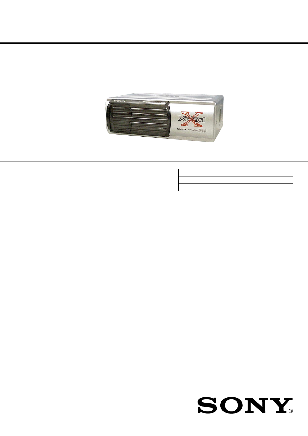
CDX-757MX
SERVICE MANUAL
Ver 1.1 2002.08
SPECIFICATIONS
US Model
Canadian Model
E Model
Model Name Using Similar Mechanism CDX-747X
CD Drive Mechanism Type MG-251B-137
Optical Pick-up Name KSS-720A
System Compact disc digital audio system
Laser diode properties Material: GaAlAs
*
This output is the value measured at a distance of 200 mm
from the objective lens surface on the Optical Pick-up Block.
Frequency response 5 – 20,000 Hz
Wow and flutter Below the measurable limit
Signal-to-noise ratio 102 dB
Outputs BUS control output (8 pins)
Current drain 800 mA (during CD playback)
Operating temperature –10°C to +55°C (14°F to 131°F)
Dimensions Approx. 262 × 90 × 185 mm
Mass Approx. 2.1 kg (4 lb. 10 oz.)
Power requirement 12 V DC car battery
Supplied accessories Disc magazine (1)
Design and specifications are subject to change without
notice.
Wavelength: 780 nm
Emission Duration: Continuous
Laser out-put Power: Less than
44.6 µW*
Analog audio output (RCA pin)
800 mA (during loading or ejecting
a disc)
3
(10
/8 × 3 5/8 × 7 3/8 in.)
(w/h/d) not incl. projecting parts
and controls
(negative ground)
Parts for installation and
connections (1 set)
9-873-618-02 Sony Corporation
2002H0500-1 e Vehicle Company
C 2002.08 Published by Sony Engineering Corporation
COMPACT DISC CHANGER
Page 2
CDX-757MX
L
SERVICING NOTES
NOTES ON HANDLING THE OPTICAL PICKUP BLOCK OR BASE UNIT
The laser diode in the optical pick-up block may suffer electrostatic breakdown because of the potential difference generated by
the charged electrostatic load, etc. on clothing and the human body .
During repair, pay attention to electrostatic breakdown and also
use the procedure in the printed matter which is included in the
repair parts.
The flexible board is easily damaged and should be handled with
care.
NOTES ON LASER DIODE EMISSION CHECK
The laser beam on this model is concentrated so as to be focused
on the disc reflective surface by the objective lens in the optical
pick-up block. Therefore, when checking the laser diode emission, observe from more than 30 cm away from the objectiv e lens.
US/Canadian model:
If the optical pick-up block is defective, please replace the whole
optical pick-up block.
Never turn the semi-fixed resistor located at the side of optical
pick-up block.
OPTICA
PICK-UP
BLOCK
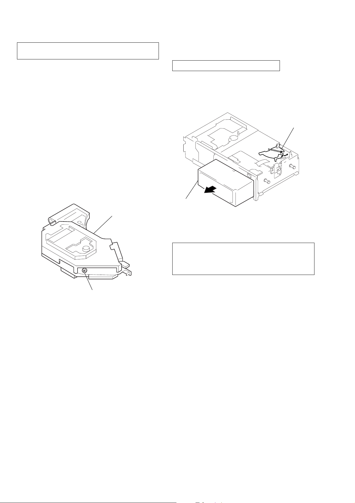
DISC MAGAZINE GETTING OUT PROCEDURE
ON THE POWER SUPPLY IS OFF
Remove the CASE (LOWER. T) beforehand
1) Press the lever (ML.S) assy in the direction of arrow A.
2) Removal the magazine assy.
Note: Take out the magazine only when the tray is completely within the
magazine. If the disk or tray is sticking out, turn on the power and
eject the magazine.
Lever (ML.S)
A
Magazine assy
SEMI-FIXED
RESISTOR
CAUTION
Use of controls or adjustments or performance of procedures
other than those specified herein may result in hazardous radiation exposure.
Flexible Circuit Board Repairing
•Keep the temperature of the soldering iron around 270 ˚C during repairing.
• Do not touch the soldering iron on the same conductor of the
circuit board (within 3 times).
• Be careful not to apply force on the conductor when soldering
or unsoldering.
Notes on chip component replacement
•Never reuse a disconnected chip component.
• Notice that the minus side of a tantalum capacitor may be damaged by heat.
SAFETY-RELATED COMPONENT WARNING!!
COMPONENTS IDENTIFIED BY MARK 0 OR DOTTED
LINE WITH MARK 0 ON THE SCHEMATIC DIA GRAMS
AND IN THE PARTS LIST ARE CRITICAL TO SAFE
OPERATION. REPLACE THESE COMPONENTS WITH
SONY PARTS WHOSE PART NUMBERS APPEAR AS
SHOWN IN THIS MANUAL OR IN SUPPLEMENTS PUBLISHED BY SONY.
ATTENTION AU COMPOSANT AYANT RAPPORT
À LA SÉCURITÉ!
LES COMPOSANTS IDENTIFIÉS P AR UNE MARQUE 0
SUR LES DIAGRAMMES SCHÉMATIQUES ET LA LISTE
DES PIÈCES SONT CRITIQUES POUR LA SÉCURITÉ
DE FONCTIONNEMENT. NE REMPLACER CES COMPOSANTS QUE PAR DES PIÈCES SONY DONT LES
NUMÉROS SONT DONNÉS DANS CE MANUEL OU
DANS LES SUPPLÉMENTS PUBLIÉS PAR SONY.
2
Page 3
CDX-757MX
TEST DISC
This set can playback a CD-R, CD-RW for audio use. When test
this set, use the following test disc.
Test disc for CD-R: TCD-R082LMT (Part No.: J-2502-063-1)
Test disc for CD-RW: TCD-W082L (Part No.: J-2502-063-2)
Notes on CD-R/CD-RW discs
•
You can play CD-Rs/CD-RWs (recordable CDs/rewritable CDs) on
this unit (fig. E).
•
Some CD-Rs/CD-RWs (depending on the equipment used for its
recording or the condition of the disc) may not play on this unit.
•
You cannot play a CD-R/CD-RW that is not finalized*.
•
A CD-R/CD-RW to which a session can be added can be played.
*
A process necessary for a recorded CD-R/CD-RW disc to be played
on the audio CD player.
E
Audio CD
MP3 files
About MP3 files
Folder (album)
1
1
MP3 file (track)
2
2
3
3
4
5
6
6
7
4
5
7
8
8
9
Tree 1 Tree 2 Tree 3 Tree 4 Tree 5
(root)
MP3 (MPEG 1 Audio Layer-3) is a standard technology and format for
compressing a sound sequence. The file is compressed to about 1/10 of its
original size. Sounds outside the range of human hearing are compressed
while the sounds we can hear are not compressed.
Notes on discs
You can play MP3 files recorded on CD-ROMs, CD-Rs (recordable CDs),
and CD-RWs (rewritable CDs). The disc must be in the ISO 9660*
level 2 format, or Joliet or Romeo in the expansion format. You can use a
disc recorded in Multi Session*
*1ISO 9660 Format
The most common international standard for the logical format of files
and folders on a CD-ROM.
There are several specification levels. In Level 1, file names must be in
the 8.3 format (no more than eight characters in the name, no more than
three characters in the extension “.MP3”) and in capital letters. Folder
names can be no longer than eight characters. There can be no more
than eight nested folder levels.
In level 2, file names can be up to 31 characters long (including the
delimiter, the dot “.”, and the extension “. MP3”). Each folder can have
up to 8 trees.
For Joliet or Romeo in the expansion format, make sure of the contents
of the writing software, etc.
*2Multi Session
This is a recording method that enables adding of data using the TrackAt-Once method. Conventional CDs begin at a CD control area called
the Lead-in and end at an area called Lead-out. A Multi Session CD is a
CD having multiple sessions, with each segment from Lead-in to Leadout regarded as a single session.
CD-Extra: A format that contains audio tracks (audio CD data) in
Session 1, and a data track in Session 2.
Mixed CD: A format that contains a data track and audio tracks (audio
Notes
• If MP3 files and Audio data are mixed in a disc, the first identified
• With formats other than ISO 9660 level 1, folder names or file
• When naming, be sure to add the file extension “.MP3” to the file
• If you put the extension “.MP3” to a file other than MP3, the unit
The playback order of the MP3 files
The playback order of the folders and files is shown in the illustration
above.
Notes
•A folder that does not include an MP3 file is skipped.
•If you playback an MP3 file before the information on all the CDs
• The unit reads the disc information (the number of folders and
•When a disc magazine is inserted into the CD changer or the reset
• The following discs take a longer time to start playback.
• Depending on the condition of the disc, it may not play back. For
•Maximum folder number in a disc: 255
•Maximum file number in a disc: 511
Cautions when playing a disc that is recorded in Multi Session
• When the first track of the first session is audio CD data: Non-music data
• When the first track of the first session is not audio CD data:
Note on character codes
Character codes vary depending on the master unit.
For details, refer to the operating instructions for the master unit.
Note on display of playing time
In the following cases, elapsed playing time may not be displayed
accurately.
– when an MP3 file of VBR (variable bit rate) is played.
– during fast-forward/reverse.
Tip
• To specify a desired playback order, before the folder or file
•A disc/album/track name or track number that is over 99 may not
CD data) in a session.
file or data will be played back.
names may not be displayed correctly.
name.
cannot recognize the file properly and will generate random noise
that could damage your speakers.
in the disc magazine has been read, and then set the ignition to
OFF or select another source, the beginning of the current track
may play back when you resume playback.
files, or the location of the data) before playback of an MP3 file. It
may take more time to start playback of a disc with a complex file
structure.
button of the connected car audio is pressed, the unit will
automatically be activated and read the information on the CDs.
When the information on all the CDs in the disc magazine has
been read, the unit will automatically stop operation. The unit
firstly reads all of the disc information in the disc magazine.
Depending on the recording method, it may take some time to
stop the operation even if you set the ignition key to OFF during
disc reading. This is not a malfunction.
–a disc recorded with complicated tree structure.
–a disc recorded in Multi Session.
–a disc to which data can be added.
We recommend that you make only one or two trees for each disc.
details, please refer to “Notes on discs.”
empty folders)
* Maximum number of files and folders: 512
When a file/folder name contains many characters, this number
may become less than 512.
information (track number, time, etc.) is displayed with no sound.
– Audio CD data is played back normally; other data is played back with
no sound. (MP3 file(s) cannot be played back.)
– If no MP3 file is in the disc, “NO Music” is displayed and nothing is
played back. (Audio CD data is not recognized.)
name, input the order by number (e.g., “01,” “02”), then record
contents onto a disc. (The order differs depending on the writing
software.)
be displayed accurately when this unit is connected to a master
unit that does not support MP3. A master unit that supports MP3
is recommended.
About ID3 tag version 2
Although not a malfunction, the following occurs when
an MP3 file containing ID3 tag ver.2 is played:
– When skipping a portion of ID3 tag ver.2 (at the
beginning of the track), sound is not output.
Skip time changes depending ID3 tag ver.2 capacity.
Example: At 64 kbytes, it is about 2 seconds
(with RealJukebox).
– The displayed elapsed playing time when skipping a
portion of ID3 tag ver.2 is inaccurate.
For MP3 files of a bit rate other than 128 kbps, time is
not displayed accurately during playback.
– When an MP3 file is created with MP3 conversion
software (ex. RealJukebox*), ID3 tag ver.2 will
automatically be written.
* “RealJukebox is a registered trademark of
RealNetworks, Inc.”
As of December, 2001
2
.
*
(including root folder and
*
1
level 1 or
3
Page 4
CDX-757MX
FAQ- about MP3 Audio File
Q1 What is MP3?
MP3 (MPEG Audio Layer3) is a standard
for compressing audio parts of Moving
Pictures Experts Group (MPEG).
The special feature of MP3 is that the music
data is compressed to about 1/10 of its
original size while retaining the same
sound quality as a CD or an MD.
Compared with an audio disc (maximum
74 minutes running time), MP3 lets you
compress about 10 audio discs or 160 fourminute songs into a CD-R/RW of 650MB.
Note
Recorded music is limited to private use only. Use
of music beyond this limit requires the permission
of the copyright holders. Copyright law prohibits
copying, distributing, or delivering all or part of
the contents.
Q2 What kind of MP3 files can be
played back?
MP3 files in CD-ROMs, CD-Rs, and CDRWs can be played.
Pay attention to the following points when
creating MP3 data CDs using your
computer, CD-R/RW drive, writing
software, or MP3 file.
• The file must be in the ISO 9660 level 1 or
level 2 format, or Joliet or Romeo in the
ISO 9660 expansion format.
A folder name or a file name with the
format other than ISO 9660 level 1 may
not be displayed correctly. When
creating MP3 data CDs, the format of ISO
9660 level 1 is recommended.
• When naming, be sure to add the file
extension “.MP3” to the MP3 file name.
The unit cannot recognize an MP3 file
without the extension “.MP3,” or a file
that is not MP3 format, even with the
extension “.MP3.”
Q3 Is there maximum number of
folders or files to play?
Pay attention to the maximum numbers
mentioned below.
•Maximum folder number in a disc: 255*
(including root folder and empty folders)
•Maximum file number in a disc: 511*
* Maximum number of files and folders:
512
When a file/folder name contains
many characters, this number may
become less than 512.
• The maximum number of trees which
can be played is 8.
The unit allows you to change the folders,
to play just the files in your favorite folder
repeatedly, or to play files randomly, create
folders according to artist name or album,
and put related MP3 files into folders to use
the unit as a CD changer.
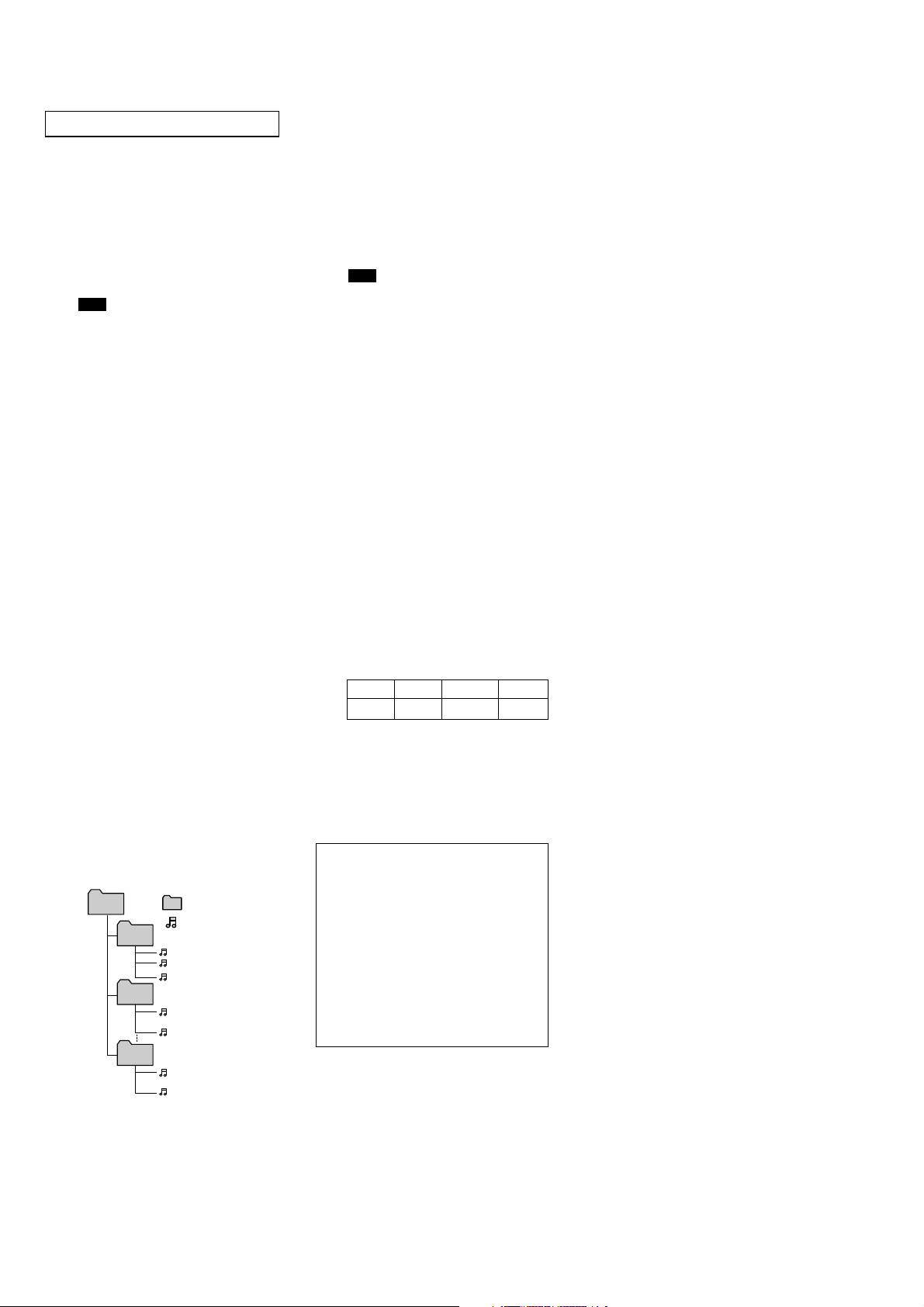
ROOT
01_
ALBUM
02_
ALBUM
10_
ALBUM
: Folder
: MP3 file
001TRACK.MP3
002TRACK.MP3
...
010TRACK.MP3
011TRACK.MP3
...
020TRACK.MP3
091TRACK.MP3
...
100TRACK.MP3
Q4 Can the unit play a data CD with
folder levels?
The unit can play a data CD with folder
levels.
Q5 Is there any restriction about the
bit rate regarding playback of
MP3 files?
There is no specific restriction, but a bit rate
of more than 128kbps is recommended
from the perspective of sound quality. The
unit also supports VBR (Variable Bit Rate).
Note
Elapsed playing time may not be displayed
accurately during cue/reverse.
Q6 Does the unit support a disk of
80 minutes running time (700
MB data capacity)?
The unit supports a disk of 80 minutes
running time (700 MB data capacity).
Q7 Can the unit play a CD-R/RW
containing both music CD data
(CD-DA) and MP3 file data?
The first identified file or data will be
played back.
Q8 Can the unit play a disc to which
data can be added (non-finalized
disc)?
The unit can play a non-finalized disc.
Q9 Can the unit play a Multi Session
disc?
The unit can play a Multi Session disc. For
details, refer to the operating instructions.
Q10 Does the unit support Emphasis?
The unit does not support Emphasis.
Q11 What is the sampling rate
supporting the unit?
The unit is supported from 16kHz to
48kHZ.
MPEG1 48kHz 44.1kHz 32kHz
MPEG2 24kHz 22.05kHz 16kHz
Q12 Does the unit support the play
list of m3u?
The unit does not support the play list of
m3u.
Q13 Does the unit support ID3-Tag?
The unit supports ID3 tag ver.1.
Pay attention to the following points about
ID3 tag ver.2.
About ID3 tag version 2
Although not a malfunction, the following occurs
when an MP3 file containing ID3 tag ver.2 is
played:
–When skipping a portion of ID3 tag ver.2 (at the
beginning of the track), sound is not output. Skip
time changes depending ID3 tag ver.2 capacity.
Example: At 64 kbytes, it is about 2 seconds
(with RealJukebox).
– The displayed elapsed playing time when skipping
a portion of ID3 tag ver.2 is inaccurate.
For MP3 files of a bit rate other than 128 kbps, time
is not displayed accurately during playback.
– When an MP3 file is created with MP3 conversion
software (ex. RealJukebox*), ID3 tag ver.2 will
automatically be written.
* “RealJukebox is a registered trademark of
RealNetworks, Inc.”
As of December, 2001
Q14 Is a file name/a folder name of
MP3 different from the name
when creating a data CD (the
name displayed on your
computer)?
On this unit, a file name/a folder name is
displayed as below.
•A file name/a folder name can be
displayed up to 8 characters.
th
or later character cannot be
A 9
displayed or scrolled.
•A folder name or a file name in a format
other than ISO 9660 level 1 may not be
displayed correctly. The file name should
only use one byte uppercase, one byte
numeric characters, or an underscore
(“__”). It should also be no more than 8
characters long, and with no more than
three characters in the extension.
• Japanese phonetic symbols/ Chinese
characters cannot be displayed.
Only one byte uppercase (A-Z), one byte
numeric character (0-9), and one byte
“_”, “.”,
symbol (
can be displayed. One byte lowercase (az) is changed to an uppercase character,
and any other characters are displayed as
“*”.
“<”, “>”, “/”, “+”, “*”)
Q15 MP3 files recorded onto a CD-R/
RW cannot be played.
This may happen in following cases.
• The recording method onto CD-R/RW is
the packet write method.
• The extension file is not an “.MP3.”
• The file data is not MP3 format.
• Some recording condition (omission of
data, etc.) or some disc condition (dirt,
crack, curving, etc.) may cause inability
to playback an MP3 file.
Q16 It takes some time to start
playback of MP3 file.
The unit reads the disc information (the
number of folders and files, or the location
of the data) before playback of MP3 file. It
may take more time to start playback of a
disc with many trees.
Please refer to the instruction manual for
details.
Q17 Playback skipping and no
playback occur.
Recording condition onto CD-R/RW
(omission of data, etc.) or disc condition
(dirt, crack, curving, etc.) may cause
playback skipping or no playback.
Q18 Can WAVE files be played back
on this unit?
WAVE files cannot be played back on this
unit.
Q19 Can other compressed formats,
such as ATRAC3, be played back
on the unit?
Only MP3 can be played back on the unit.
4
Page 5

TABLE OF CONTENTS
SERVICING NOTES .......................................................... 2
1. GENERAL
Installation....................................................................... 6
Connections..................................................................... 7
2. DISASSEMBLY
2-1. Disassembly Flow ........................................................... 8
2-2. Case (Upper. T), Front Panel Assy ................................. 9
2-3. Mechanism Deck (MG-251B-137)................................. 9
2-4. JACK Board .................................................................... 10
2-5. MAIN Board, Slide Variable Resistor
(Elevator Height Sensor) (RV202) ................................. 10
2-6. ELJ Motor Assy (Elevator) (M104) ................................ 11
2-7. Escutcheon (T) ................................................................ 11
2-8. Chassis (U.S) Sub Assy .................................................. 12
2-9. Chassis Assy.................................................................... 12
2-10. RF Board ......................................................................... 13
2-11. Sled Motor Assy (251) (M101),
Optical Pick-up (KSS-720A) .......................................... 13
2-12. LSW Board, Spindle Motor (S) Sub Assy (M102) ........ 14
2-13. ELJ Motor Assy (Chucking) (M103) ............................. 14
CDX-757MX
3. ASSEMBLY
3-1. Assembly Flow................................................................ 15
3-2. Optical Pick-up Complete Assy...................................... 15
3-3. Gear (Lomini)/(Load 1) Assy ......................................... 16
3-4. Operation Check ............................................................. 16
4. MECHANICAL ADJUSTMENT .......................... 17
5. ELECTRICAL CHECK .......................................... 18
6. DIAGRAMS
6-1. Block Diagram – SERVO Section – .............................. 20
6-2. Block Diagram – MAIN Section (1/2) – ....................... 21
6-3. Block Diagram – MAIN Section (2/2) – ....................... 22
6-4. Note for Printed Wiring Boards and
Schematic Diagrams ....................................................... 23
6-5. Printed Wiring Boards – RF/LSW Boards – ................. 24
6-6. Schematic Diagram – RF/LSW Boards –...................... 25
6-7. Printed Wiring Boards
– MAIN Board (Component Side) – .............................. 26
6-8. Printed Wiring Boards
– MAIN (Conductor Side)/SWITCH Boards –.............. 27
6-9. Schematic Diagram – MAIN Board (1/3) – .................. 28
6-10. Schematic Diagram
– MAIN (2/3)/SWITCH Boards – .................................. 29
6-11. Schematic Diagram – MAIN Board (3/3) – .................. 30
6-12. Printed Wiring Boards – JACK Board –........................ 32
6-13. Schematic Diagram – JACK Board – ............................. 33
6-14. IC Pin Function Description ........................................... 39
7. EXPLODED VIEWS
7-1. Case Section .................................................................... 41
7-2. Mechanism Deck Section-1 (MG-251B-137) ................ 42
7-3. Mechanism Deck Section-2 (MG-251B-137) ................ 43
7-4. Mechanism Deck Section-3 (MG-251B-137) ................ 44
7-5. Mechanism Deck Section-4 (MG-251B-137) ................ 45
8. ELECTRICAL PARTS LIST ............................... 46
5
Page 6
CDX-757MX
SECTION 1
GENERAL
This section is extracted from
instruction manual.
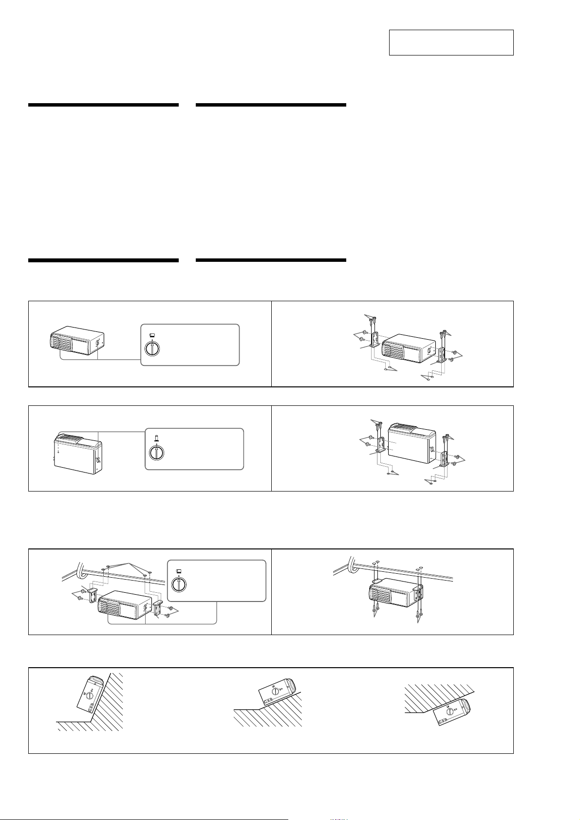
InstallationInstallation
Precautions
• Choose the mounting location carefully, observing the following:
— The unit is not subject to temperatures exceeding 55°C (131°F)
(such as in a car parked in direct sunlight).
— The unit is not subject to direct sunlight.
— The unit is not near heat sources (such as heaters).
— The unit is not exposed to rain or moisture.
— The unit is not exposed to excessive dust or dirt.
— The unit is not subject to excessive vibration.
— The fuel tank should not be damaged by the tapping screws.
— There should be no wire harnesses or pipes under the place
where you are going to install the unit.
— The spare tire, tools or other equipment in or under the trunk
should not be interfered with or damaged by the screws or the
unit itself.
• Be sure to use only the supplied mounting hardware for a safe and
secure installation.
• Use only the supplied screws.
• Make holes of ¿ 3.5 mm (
nothing on the other side of the mounting surface.
How to install the unit
The brackets 1 provide two positions for mounting, high and low.
Use the appropriate screw holes according to your preference.
5
/32 in.) only after making sure there is
Horizontal installation
1
HORIZONTAL
Précautions
• Choisir l’emplacement de montage en tenant compte des
observations suivantes :
— Appareil non soumis à des températures dépassant 55°C (131°F)
(comme dans une voiture garée au soleil).
— Appareil non soumis au rayonnement solaire direct.
— Appareil à l’écart de sources de chaleur (comme des radiateurs).
— Appareil non exposé à la pluie ou à l’humidité.
— Appareil non exposé à des poussières ou à des souillures en
excès.
— Appareil non exposé à des vibrations excessives.
— Vérifier que le réservoir d’essence ne risque pas d’être
endommagé par les vis taraudeuses.
— Il ne doit pas y avoir de faisceau de fils ou de tuyaux à
l’emplacement du montage.
— Vérifier que l’appareil ou les vis ne risquent pas d’endommager
ou de gêner la roue de secours, les outils, ou autre objet dans le
coffre.
• Pour garantir la sécurité de l’installation, utiliser uniquement le
matériel de montage fourni.
• Utilisez uniquement les vis fournies.
• Ne percez les trous de 3,5 mm (
qu'il n'y avait rien de l'autre côté de la surface de montage.
Installation de l’appareil
Les supports 1 offrent deux positions de montage, haut et bas.
Utilisez les trous de vissage appropriés en fonction de vos préférences.
5
/32 po.)¿ qu'après vous être assuré
Installation horizontale
2
Align with the marked position.
Aligner sur le repère.
Unit: mm (in.)
Unité : mm (po.)
3
2
1
5
/32)
¿ 3.5 (
3
2
1
Vertical installation Installation verticale
1
Align with the marked position.
VERTICAL
Aligner sur le repère.
Suspended installation
When the unit is to be installed under the rear tray etc. in the trunk
compartment, make sure the following provisions are made.
• Choose the mounting location carefully so that the unit can be
installed horizontally.
• Make sure the unit does not hinder the movement of the torsion bar
spring etc. of the trunk lid.
1
¿ 3.5 (5/32)
1
2
Unit: mm (in.)
Unité : mm (po.)
Unidad: mm
1
Inclined installation
After installing the unit, align the dials with one of the marks so that the
arrows are as vertical as possible.
Installation suspendue
Si l’appareil doit être installé sous la plage arrière dans le coffre, par
exemple, observer les précautions suivantes.
• Bien choisir l’emplacement pour pouvoir installer l’appareil à
l’horizontale.
• Vérifier que l’appareil ne gêne pas les mouvements du ressort de
fermeture du coffre, entre autres.
Align with the marked position.
HORIZONTAL
Aligner sur le repère.
Alinee en la posición marcada.
2
Installation inclinée
Après avoir installé l’appareil, alignez les disques sur un repère de
façon à ce que les flèches soient dans la position la plus verticale
possible.
2
Unit: mm (in.)
Unité : mm (po.)
3
2
1
¿ 3.5 (5/32)
3
2
1
2
3
3
V
ER
T
I
CA
L
L
TA
N
ZO
I
R
HO
Note
Be sure to align the left and right dials with the same mark.
6
L
A
T
N
O
Z
I
R
O
V
H
E
R
T
I
C
A
L
Remarque
Veillez à aligner les disques gauche et droite sur le même repère.
L
A
T
N
O
Z
I
R
O
V
H
E
R
T
I
C
A
L
Page 7
Connections/Connexions
CDX-757MX
Connection diagram/Schéma de connexion
Sony BUS compatible car audio
Autoradio compatible BUS Sony
BUS AUDIO IN BUS CONTROL IN
45
CDX-757MX
Inserting a disc/Insertion d’un disque
1
With the arrow side facing up
Avec la partie fléchée tournée vers le haut
c
Tab
Onglet
Labeled surface up
Etiquette vers le haut
10 discs, one in each tray
10 disques, un par plateau
For details, refer to the Installation/Connections manual of the car audio.
Pour plus de détails, consulter le manuel d’installation/connexions de
l’autoradio.
Note
For connecting two or more changers, the XA-C30 source selector (optional) is necessary.
Remarque
Pour raccorder deux ou plusieurs changeurs, le sélecteur de source XA-C30 (en option)
est nécessaire.
Note
You cannot play 8cm (3 in.) CDs.
Remarque
Vous ne pouvez pas écouter de CD de 8 cm (3po.) sur ce lecteur.
Use the supplied disc magazine or the disc
magazine XA-250.The disc magazine XA-10B/XA350 can not be used with this unit.If you use any
other magazine,it may cause a malfunction.
Utilisez le magasin à disques fourni ou un magasin à
disques XA-250. Vous ne pouvez pas utiliser de
magasin à disques XA-10B/XA-350 avec cet appareil.
L'utilisation d'un autre type de magasin à disques
risque de provoquer un dysfonctionnement.
2
Push to unlock the door
Poussez pour déverrouiller la porte
c
3
Disc magazine
Chargeur de disques
4
Notes on the disc magazine
•Do not leave the disc magazine in locations with high temperatures
and high humidity such as on a car dashboard or in the rear
window where the disc magazine will be subjected to direct
sunlight.
•Do not place more than one disc at a time onto one tray, otherwise
the changer and the discs may be damaged.
•Do not drop the disc magazine or subject it to a violent shock.
When the tray comes out
Normally, the trays will not come out of the magazine. However, if they are
pulled out of the magazine, it is easy to re-insert them.
Lorsque le plateau sort
En principe, les plateaux ne sortent pas du chargeur. Toutefois, s’ils sortent du
chargeur, il est facile de les réinsérer.
To remove
Retrait
Use the unit with the door closed completely
Otherwise, foreign matter may enter the unit and
contaminate the lenses inside the changer.
Utilisez cet appareil avec la fenêtre
complètement fermée
Sinon, des corps étrangers pourraient pénétrer dans
l’appareil et encrasser les lentilles dans le lecteur.
Slide open
Coulissez pour ouvrir
Z (EJECT)
Remarques sur le chargeur de disques
•Ne pas laisser le chargeur de disques dans un endroit très chaud ou
très humide comme sur le tableau de bord ou sur la plage arrière de
la voiture où il serait en plein soleil.
•Ne pas insérer plus d’un disque à la fois sur le plateau, sinon le
changeur et les disques risquent d’être endommagés.
•Ne pas laisser tomber le chargeur de disques ni le cogner.
Note
To prevent injury, do not insert your hand in the CD changer.
Remarque
Pour éviter toute blessure, ne pas introduire la main dans le
changeur de CD.
If the disc magazine does not lock properly
Take out the magazine, and after pressing the Z (EJECT) button,
re-insert it.
Si vous ne pouvez pas fermer le chargeur de disques
Sortez le chargeur et, après avoir appuyé sur la touche Z (EJECT),
réinsérez-le.
Note
When a disc magazine is inserted into the CD changer or the reset button of the connected car audio is pressed, the unit will
automatically be activated and read the information on the CDs. When the information on all the CDs in the disc magazine has been
read, the unit will automatically stop operation. The unit firstly reads all of the disc information in the disc magazine. Depending on
the recording method, it may take some time to stop the operation even if you set the ignition key to OFF during disc reading. This is
not a malfunction.
Remarque
Quand un chargeur de disques est inséré dans le changeur de CD ou si la touche de réinitialisation de l’autoradio raccordé est
enclenchée, l’appareil se met automatiquement en marche et reproduit les CD. Lorsque tous les CD du chargeur ont été reproduits,
l’appareil s’arrête automatiqement. L’appareil commence par lire toutes les informations relatives au disque dans le chargeur de
disque. Selon la méthode d’enregistrement, l’arrêt de l’opération peut demander quelques instants avant de s’arrêter si vous tournez
la clé de contact sur OFF au cours de la lecture du disque. Il ne s’agit pas d’un dysfonctionnement.
With the cut-away portion of the tray facing you, insert the right corner of the tray in
the slot, then push in the left corner until it clicks.
Note
Do not insert the tray upside down or in the wrong direction.
Avec la portion découpée du plateau vous faisant face, insérer le coin droit du plateau
dans la fente, puis enfoncer le coin gauche jusqu’au déclic.
Remarque
Ne pas insérer le plateau à l’envers ou dans le mauvais sens.
7
Page 8
CDX-757MX
SECTION 2
DISASSEMBLY
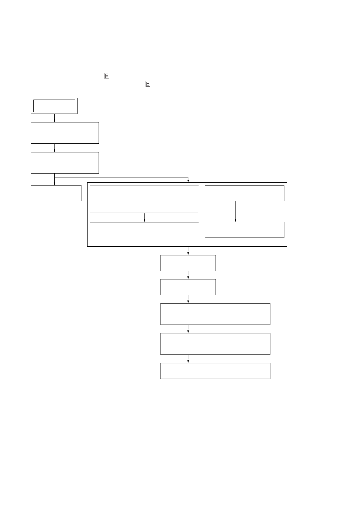
• This set can be disassembled in the order shown below.
2-1. DISASSEMBLY FLOW
Note 1: The process described in can be performed in any order.
Note 2: Without completing the process described in , the next process can not be performed.
SET
2-2. CASE (UPPER.T),
FRONT PANEL ASSY
(Page 9)
2-3. MECHANISM DECK
(MG-251B-137)
(Page 9)
2-4. JACK BOARD
(Page 10)
2-5. MAIN BOARD,
SLIDE VARIABLE RESISTOR
(ELEVATOR HEIGHT SENSOR) (RV202)
(Page 10)
2-6. ELJ MOTOR ASSY
(ELEVATOR) (M104)
(Page 11)
2-9. CHASSIS ASSY
2-10. RF BOARD
2-11. SLED MOTOR ASSY (251) (M101),
2-12. LSW BOARD,
2-7. ESCUTCHEON (T)
(Page 11)
2-8. CHASSIS (U.S) SUB ASSY
(Page 12)
(Page 12)
(Page 13)
OPTICAL PICK-UP (KSS-720A)
(Page 13)
SPINDLE MOTOR (S) SUB ASSY (M102)
(Page 14)
2-13. ELJ MOTOR ASSY (CHUCKING) (M103)
(Page 14)
8
Page 9
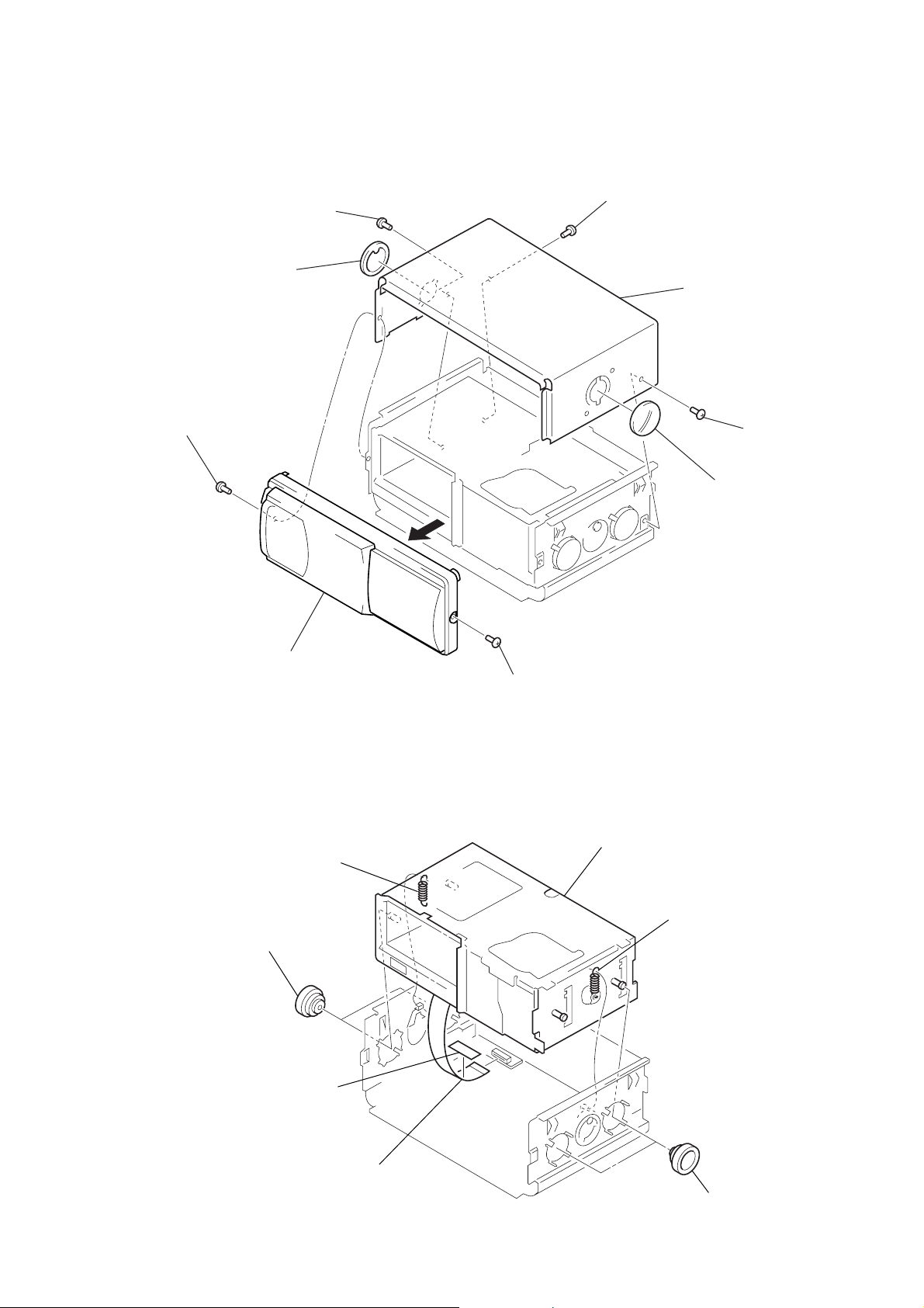
Note: Follow the disassembly procedure in the numerical order given.
3
screw
(PTT2.6
×
6)
4
lever (FLT. 838)
3
screw (PTT2.6 × 6)
3
screw (PTT2.6 × 6)
1
screw (PTT2.6 × 6)
1
screw
(PTT2.6
×
6)
2
front panel assy
4
lever (FLT. 838)
5
case (upper. T)
)
)
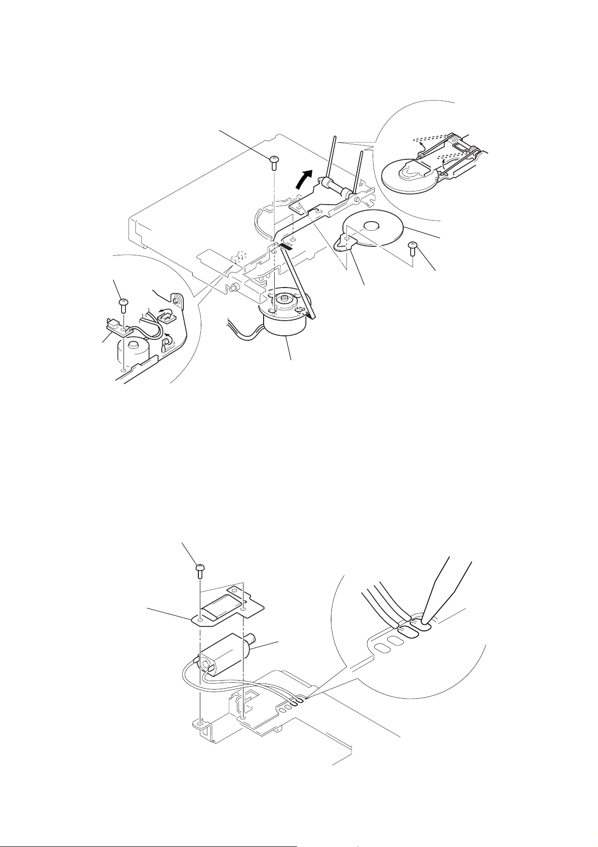
2-2. CASE (UPPER. T), FRONT PANEL ASSY
CDX-757MX
2-3. MECHANISM DECK (MG-251B-137)
2
tension coil spring (FL)
1
two dampers (T)
filament tape
3
jack flexible board
(CNJ901)
4
mechanism deck (MG-251B-137)
2
tension coil spring (FL
1
two dampers (T
9
Page 10
CDX-757MX
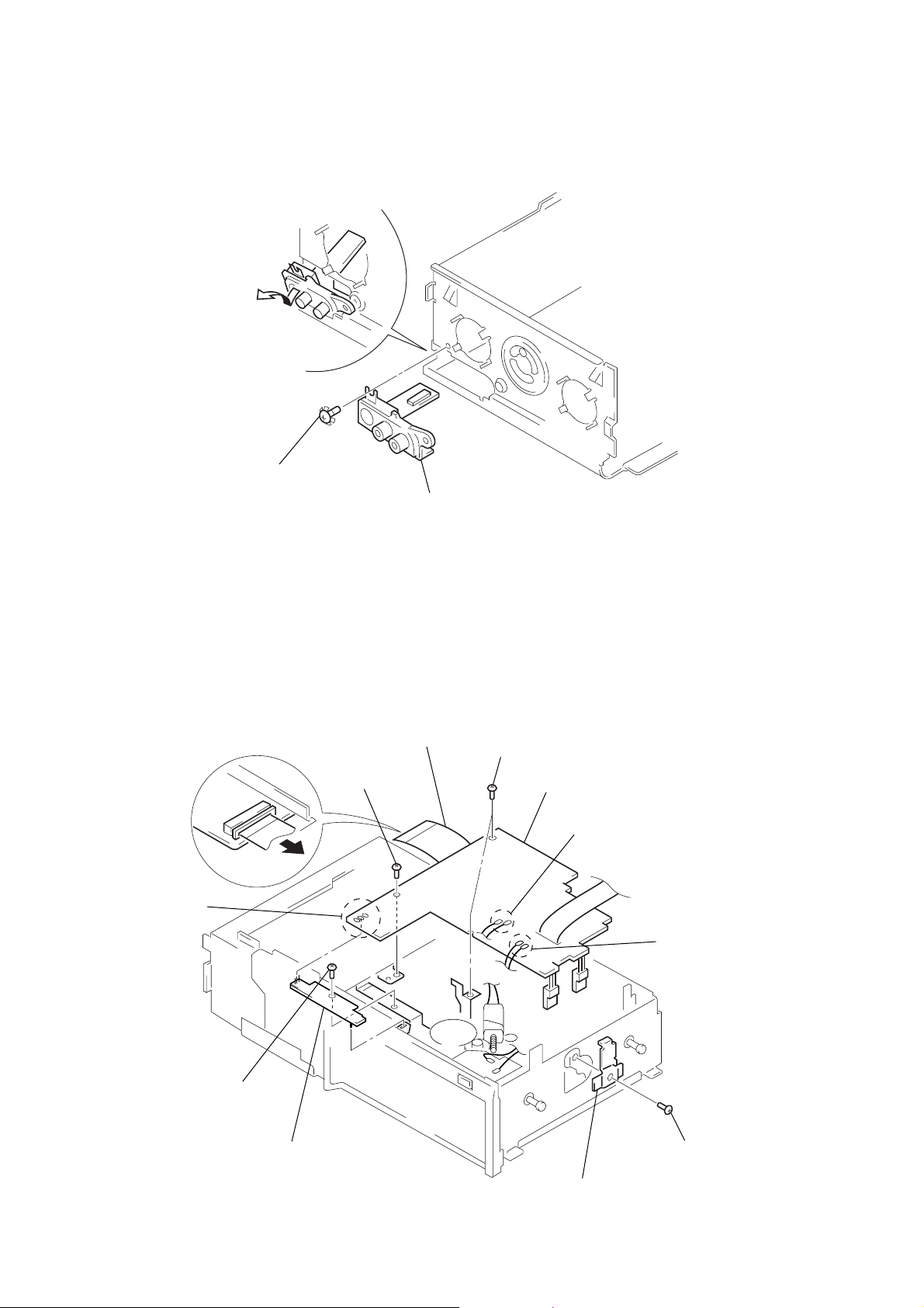
2-4. JACK BOARD
Remove the jack board of
the arrow.
1
ground point screw
(PTT2.6
×
6)
2
jack board
2-5. MAIN BOARD , SLIDE V ARIABLE RESIST OR (ELEV A T OR HEIGHT SENSOR) (RV202)
1
main flexible board
2
Remove three solders of
the slide variable resistor
(RV202).
5
screw (FP)
(CNJ101)
5
two screws (FP)
6
main board
2
Remove two solders of
the elevator motor leads (M104).
2
Remove two solders of
the switch board leads.
10
7
screw
(PTT2
×
4)
8
slide variable resistor
(elevator height sensor)
(RV202)
4
heat sink (T)
3
screw (PTT2 × 4)
Page 11
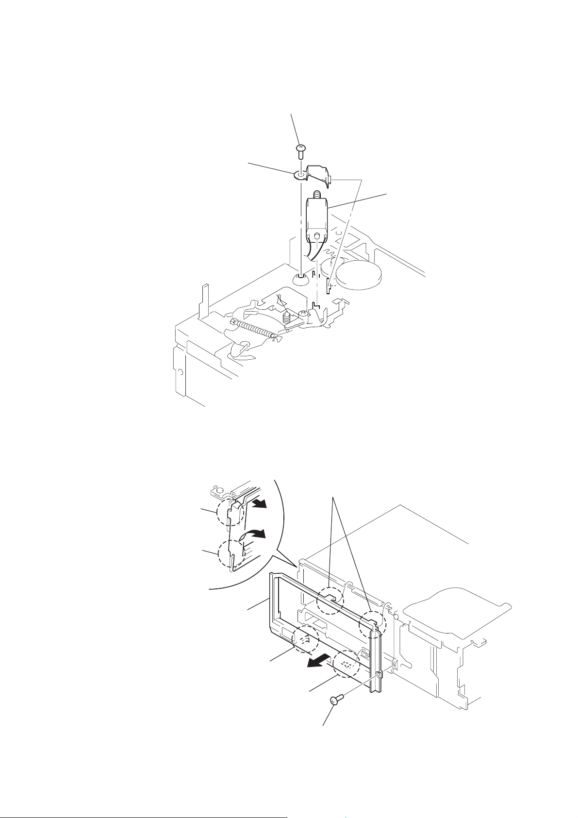
2-6. ELJ MOTOR ASSY (ELEVATOR) (M104)
1
2
bracket (EVM.S)
screw
(PTT2
CDX-757MX
×
4)
3
ELJ motor assy (elevator) (M104)
2-7. ESCUTCHEON (T)
2
Remove the claw
in the direction of arrow
4
Remove the ditch
in the direction of arrow
5
Remove the escutcheon (T)
in the direction of arrow
A
B
two claws
3
.
.
C
.
3
claw
B
A
4
C
ditch
1
screw (T)
11
Page 12
CDX-757MX
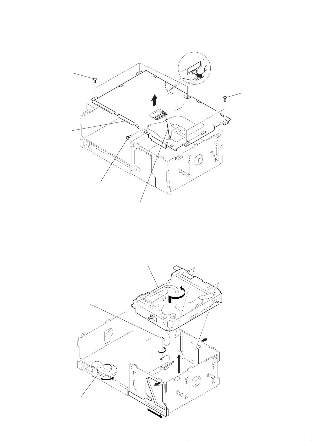
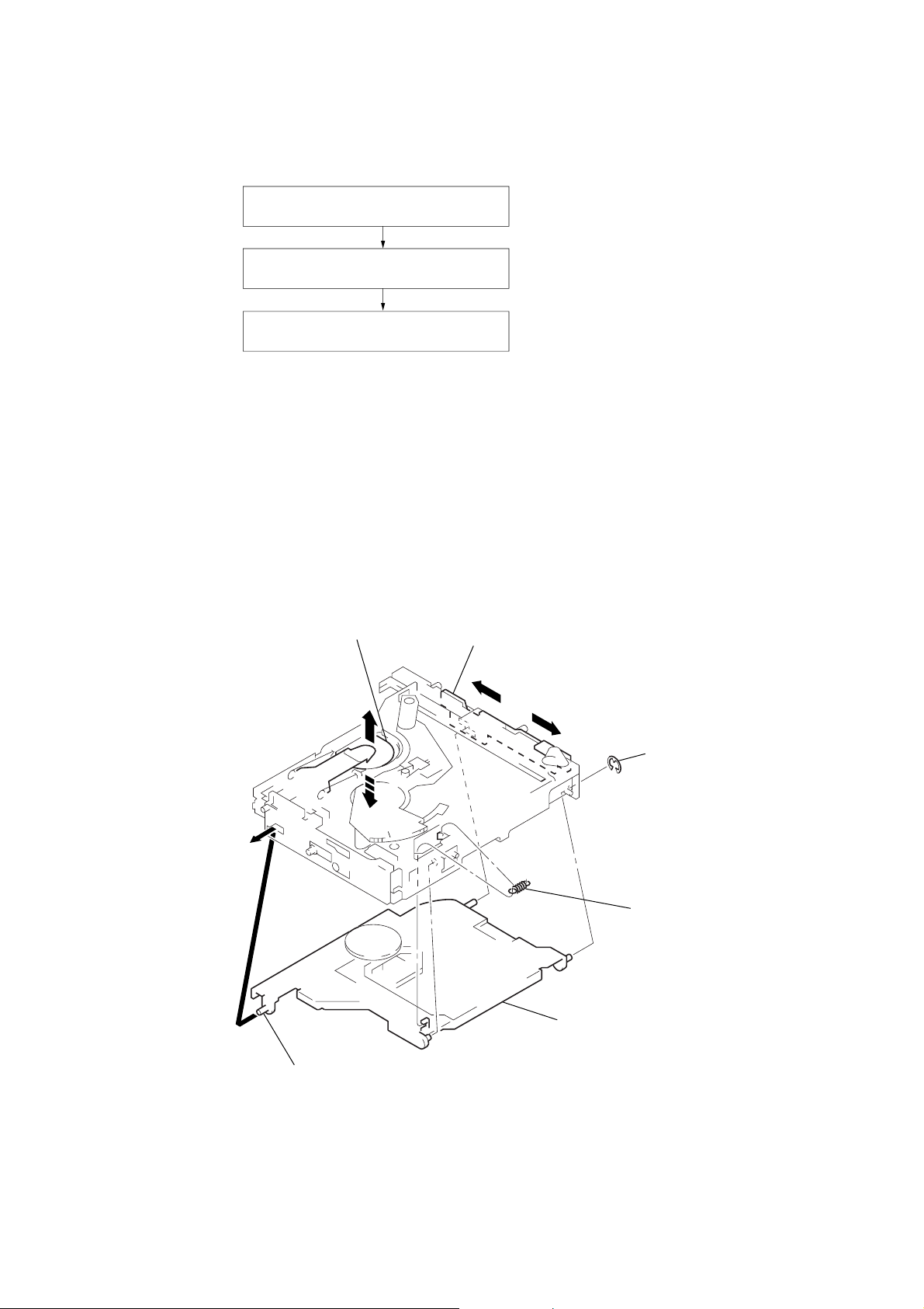
2-8. CHASSIS (U.S) SUB ASSY
1
three screws
(PTT2 × 4)
5
chassis (U.S) sub assy
3
A
2
Remove the edge
in the direction
of arrow A.
1
two screws
(PTT2 × 4)
2-9. CHASSIS ASSY
5
1
screw
(PTT2 × 4)
spring (stopper.lower)
4
spring (SUT)
6
chassis assy
4
12
1
Turn the gear (EVD.S) fully
in the direction of arrow A.
3
2
A
3
Page 13
2-10. RF BOARD
3
two screws
(PS2
CDX-757MX
×
4)
4
RF board
3
two screws
×
4)
(PS2
2
Remove four solders
of the LSW board leads
and spindle motor leads (M102).
2
Remove two solders
of the sled motor leads
(M101).
1
OP flexible board (CN102).
2-11. SLED MOTOR ASSY (251) (M101), OPTICAL PICK-UP (KSS-720A)
1
two precision screws
(P2
×
4
Turn shaft (feed) assy
in the direction
of the arrow,
then remove it.
3)
2
sled motor assy (251)
(M101)
OP flexible board
adhesive
sheet
3
optical pick-up
(KSS-720A)
optical
pick-up
Note: After connecting OP flexible board,
fix it with adhesive sheet
to optical pick-up.
13
Page 14
CDX-757MX
)
w
2-12. LSW BOARD, SPINDLE MOTOR (S) SUB ASSY (M102)
8
two precision screws
(P1.7
×
2.2)
7
1
precision screw
(P2
×
2.5)
5
bracket (CP)
spring (chucking)
3
6
retainer (disc
4
precision scre
(P2 × 2.2)
2
LSW board
2-13. ELJ MOTOR ASSY (CHUCKING) (M103)
2
two screws
(PTT2 × 4)
3
retainer (CHM)
9
Remove the spindle motor (S) sub assy (M102)
in the direction of the arrow.
1
Remove two solders of
the chucking motor leads (M103).
4
ELJ motor assy (chucking) (M103)
14
Page 15
• This set can be assembled in the order shown below.
)
3-1. ASSEMBLY FLOW
3-2. OPTICAL PICK-UP COMPLETE ASSY
(Page 15)
3-3. GEAR (LOMINI) / (LOAD 1) ASSY
(Page 16)
3-4. OPERATION CHECK
(Page 16)
CDX-757MX
SECTION 3
ASSEMBLY
3-2. OPTICAL PICK-UP COMPLETE ASSY
1
chuck plate
Move the lever (LOCK 3A) in the direction of arrow A,
and return it a little in the direction of arrow
from the position where the chuck plate is moved
down to the lower limit.
B
A
B
3
stop ring 2.0 (E type
4
tension spring (DH)
shaft (A)
2
optical pick-up complete assy
Note: Insert the shaft (A) first.
15
Page 16
CDX-757MX
3-3. GEAR (LOMINI)/(LOAD 1) ASSY
gear (LOAD 2)
marking
Fig. A
3
Attach the gear (LOAD 1) assy
with its facing inside.
gear (LOMINI)
slit
chuck plate
2
Attach the gear (LOMINI) at the position
shown in Fig. A.
shaft (rotary prevention C)
1
B
stop ring 1.5 (E type)
4
Move the lever (LOCK 3A)
fully in the direction of arrow
to move the chuck plate up.
B
3-4. OPERATION CHECK
1
Confirm that the slider moves in the direction of arrow C to move down
the chuck plate if the gear (LOAD 1) is rotated in the direction of arrow
or the chuck plate moves up and the slider moves in the direction of
arrow D if the gear is rotated in the direction of arrow B.
chuck plate
A
slider
D
C
16
A
gear (LOAD 1) assy
B
Page 17
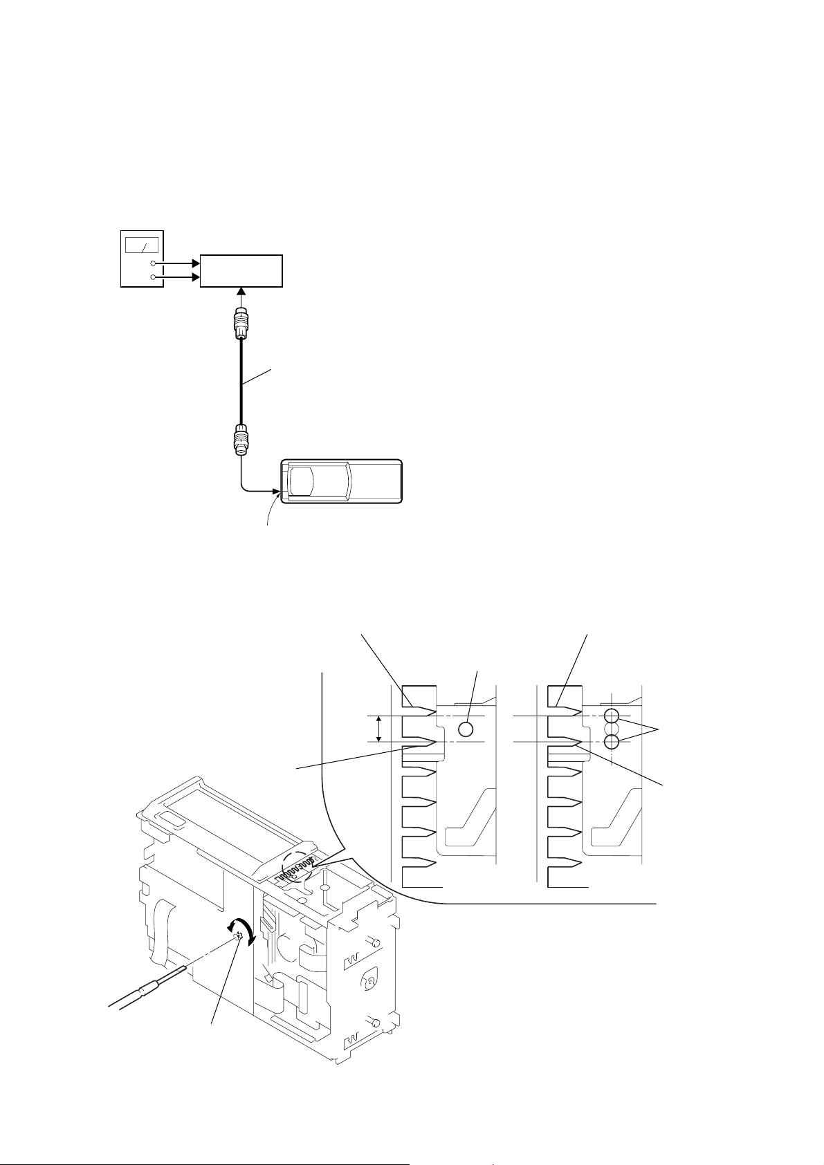
MECHANICAL ADJUSTMENT
• Elevator Height (Address) Adjustment
CDX-757MX
SECTION 4
Note: This adjustments is necessary when the system controller (IC201),
variable resistor (RV201), slider (R), slider (L), or chassis (ELV)
was replaced for any repair.
Connection:
power supply
(DC 14.4 V)
master unit
+
GND
BUS cable
compact disc changer
CONTROL connector
(CN901)
Adjustment Method:
1. Connect this set to the master unit (e.g. MDX-C7970), load a
disc magazine, and place the set vertically as shown below.
2. Connect the regulated power supply to the master unit, and
turn the power on.
3. Press the DISC button on the master unit and select DISC 5.
4. At this time, if the elevator shaft does not position between
comb teeth A and B at addresses 5 and 6 as shown below,
adjust the following.
5. Press repeatedly the DISC + and – buttons on the master unit
so that the elevator shafts moves from address 6 to address 5,
or from 5 to 6. At this time, adjust RV201 on the main board
so that the elevator shaft positions smoothly between comb
teeth A and B.
6. Further, place the set horizontally and make same adjustment
as mentioned above.
7. After adjustment at addresses 5 to 6 is finished, check all operations from addresses 1 to 10 with the set placed vertically
and horizontally respectively to confirm that the ele vator shaft
positions in a range between comb teeth A to B.
comb tooth at address 6
comb tooth at address 5
comb tooth at address 6
elevator shaft
A
B
OK NG
A
elevator shaft
B
comb tooth at address 5
RV201
17
Page 18
CDX-757MX
SECTION 5
ELECTRICAL CHECK
Note:
1. This check is performed with the set placed horizontally.
2. Power supply voltage: DC14.4 V (more than 3 A).
3. Be sure to use the disc “YEDS-18” parts code: 3-702-101-01, but only
when indicated.
4. Use a master unit that supports SONY bus system.
Connection:
power supply
(DC 14.4 V)
master unit
+
GND
BUS cable
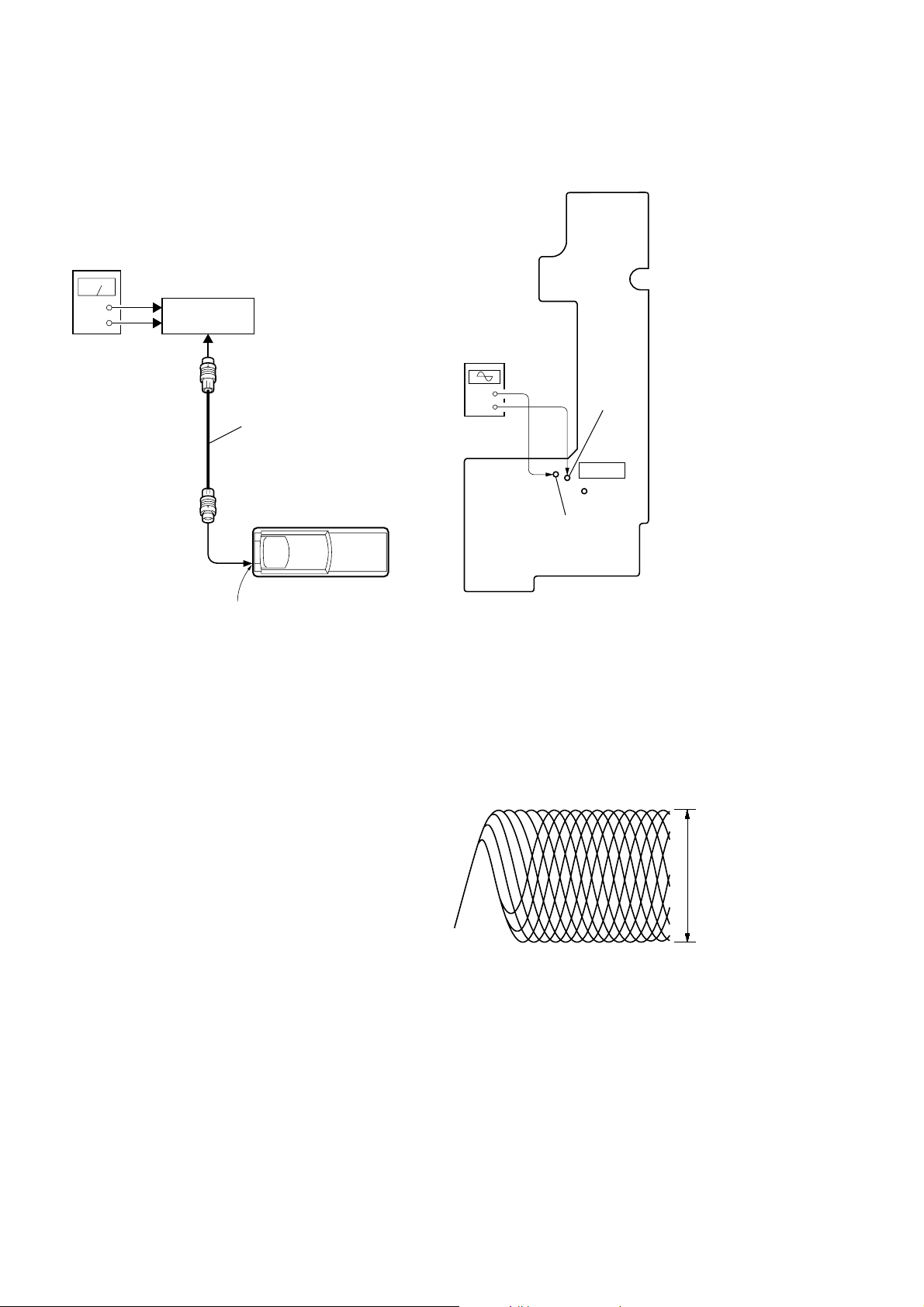
FOCUS BIAS CHECK
Connection:
– RF Board (Component Side) –
oscilloscope
(AC range)
+
–
TP (RFAC)
TP (VC)
IC101
compact disc changer
CONTROL connector
(CN901)
Procedure:
1. Connect the oscilloscope to TP (RFAC) and TP (VC) on the
RF board.
2. Put the set into play mode by loading the disc (YEDS-18).
3. Confirm that oscilloscope waveform is clear and check RF signal level is correct or not.
Note:
Clear RF signal waveform means that the shape “◊” can be clearly distinguished at the center of the waveform.
RF signal waveform
VOLT/DIV: 200 mV
TIME/DIV: 500 ns
(10 : 1 probe in use)
level: 1.4 ± 0.3 Vp-p
When observing the eye pattern, set the oscilloscope to AC range
and raise the vertical sensitivity so that it may be easily seen.
18
Page 19
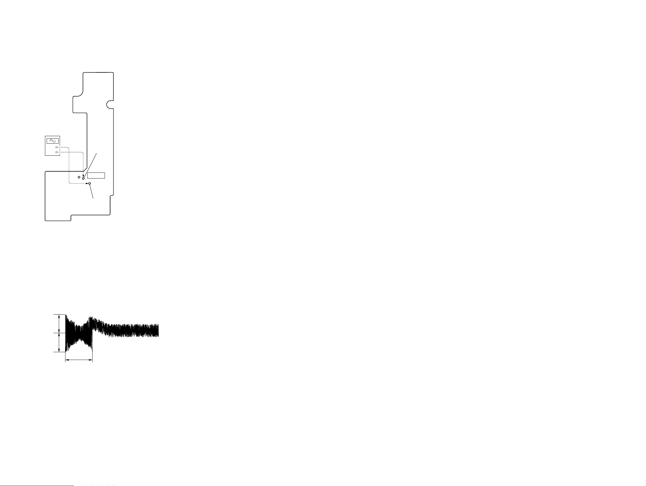
TRACKING OFFSET CHECK
Connection:
– RF Board (Component Side) –
oscilloscope
(DC range)
CDX-757MX
+
–
TP (VC)
IC101
TP (TE)
Procedure:
1. Connect the oscilloscope to TP (TE) and TP (VC) on the RF
board.
2. Put the set into play mode by loading the disc (YEDS-18).
. >
3. Press the
[ AMS ] button on the master unit, and check
the traverse waveform*.
4. Confirm that the oscilloscope waveform is symmetrical on the
top and bottom in relation to 0 V dc, and check this level.
* Traverse waveform: This is the tracking error wave form appears
when crossing the track.
Traverse waveform
A
0 V
B
VOLT/DIV: 500 mV
TIME/DIV: 2 ms
Center: 0 V
A=B
traverse waveform
(100 track jump waveform)
1919
Page 20

CDX-757MX
SECTION 6
DIAGRAMS
6-1. BLOCK DIAGRAM – SERVO Section –
DETECTOR
A
B
C
D
E
F
LASER DIODE
OPTICAL
PICK-UP BLOCK
(KSS-720A)
(TRACKING)
(FOCUS)
I-V AMP
PD LD
2-AXIS DEVICE
VC
(SLED)
(SPINDLE)
M103
(CHUHCKING)
RF AMP,
FOCUS/TRACKING ERROR AMP
A
6
B
7
C
8
D
9
E
10
F
11
AUTOMATIC
POWER
CONTROL
Q101
M101
M102
IC101
RFAC
SUMMING
AMP
SUMMING
FOCUS
ERROR
AMP
TRACKING
ERROR
1
27
TRACKING/FOCUS COIL DRIVE,
8
9
6
7
10
MM
11
12
MM
13
5
MM
4
AC
SUM
4 3
RFDC
AMP
DC OFST
RW/ROM
AMP
RW/ROM
SW
LD
VC
SLED/SPINDLE/CHUCKING
MOTOR DRIVE
VO3 +
VO3 –
VO4 +
VO4 –
VO2 +
VO2 –
VO1 +
VO1 –
VL0 +
VL0 –
APC AMP
IC201
MOTOR
COIL
DRIVE
DRIVE
COIL
DRIVE
MOTOR
DRIVE
MOTOR
DRIVE
MOTOR
DRIVE
PD
DVC
VIN3 +
VIN3 –
VIN4 +
VIN4 –
VIN2 +
VIN2 –
VIN1-B
FWD
RFDCO
12
2
14
REV
EQ IN
FE
TE
25
24
31
32
22
21
18
1
2
RFAC
VCA
RF
28
30
FE
16
TE
18
RF EQ
AMP
RF AMP OFFSET
CONTROL SWITCH
Q102
TFDR
48
TRDR
49
FFDR
50
FRDR
51
SFDR
46
SRDR
47
MDP
43
RFAC
15
D-RAM
IC102
RF
5963
CE
VC
PWM GENERATOR
DIGITAL
CLV
RFDC
OP AMP
ANALOG SW
A/D CONVERTER
SERVO DSP
71
73
74
DQ1 – DQ4
A0 – A10
RAS
CAS
WE
OE
FE
TE
FE
TE
23
22
RFAC
ASYMMETRY
CORRECTOR
ASYI
ASYO
2, 3,
24, 25
21, 8
9 – 12, 15 – 19,
5
4
61606258
SE
MIRR
DECT
FOK
FILTER
66 69 68 67
FILI
PCO
FILO
CLTV
DIGITAL
PLL
D0 – D3
118, 117
116, 115,
A0 – A10
3 – 1, 111
109 – 106, 7 – 5,
XRAS
113
XCAS
119
XWE
114
XOE
120
ON : When completion of the disc
ON : When completion of the disc
chucking operation
chucking operation
ON : When completion of the disc
ON : When completion of the disc
save operation
save operation
VIBRATION
MEMORY
CONTROLLER
&
COMPRESSION
EXPANDER
XRDE
XWRE
XQOK
ON : When the optical pick-up
ON : When the optical pick-up
is inner position
is inner position
DIGITAL SIGNAL PROCESSOR,
DIGITAL SERVO PROCESSOR,
D-RAM CONTROLLER
IC101
EFM
DEMODULATOR
INTERNAL BUS
SUBCODE
PROCESSOR
SW3
(LIMIT)
SW1
(CHUCKING END DETECT)
SW2
(SAVE END DETECT)
D/A
INTERFACE
32k RAM
ERROR
CORRECTOR
CPU
INTERFACE
SERVO AUTO
SEQUENSOR
SERVO
INTERFACE
SSTP
45
WDCK
GFS
DATA
CLOK
XLAT
SENS
SQSO
SQCK
SCOR
XRDE
XWRE
XQOK
SCLK
FOK
XRST
1578
1581
1523
1525
1524
1526
1514
1515
1517
159
158
1512
27
35
21
DIGITAL
OUT
DAC
SELECTOR
CLOCK
GENERATOR
D201
DOUT
1585
PCMDI
1589
PCMD
15
88
1588
BCK
15
90
LRCK
15
86
XTAI
1593
XTAO
1594
CD-ROM/RW
SELECT SWITCH
Q202
X101
16.9344MHz
R/RW SEL
90
GRSCOR
40
GFS
5
CDDAT
10
CDCLK
8
CDLAT
9
SENS
7
SQSO
84
SQCK
85
SCOR
38
XRDE
16
XWRE
17
XQOK
15
SYSTEM CONTROLLER
IC201 (1/3)
SCLK
6
FOK
4
XRST
11
LOADF
95
LOADR
96
LIM SW
100
LOAD SW
98
SAVE SW
99
SDO
SDI
BCK
LRCK
XTAL-IN
TCXRDE
(Page 21)
B
(Page 21)
A
(Page 21)
C
(Page 21)
D
SIGNAL PATH
: CD PLAY
2020
Page 21

6-2. BLOCK DIAGRAM – MAIN Section (1/2) –
2
1
3
MD
MC
ML
13
14
15
DATA
BCK
LRCK
MD
MC
ML
SERIAL
INPUT
INTERFACE
FUNCTION
CONTROL
INTERFACE
8 TIME OVER
SAMPLING
DIGITAL FILTER
WITH
FUNCTION
CONTROLLER
ENHANCED
MULTI-LEVEL
DELATA-SIGMA
MODULATOR
D/A
CONVERTER
OUTPUT AMP
AND
LOW-PASS
FILTER
VOUTL
VCOM
VOUTR
CDX-757MX
SIGNAL PATH
: CD PLAY
7
CN901 (1/2)
10
8
LOW-PASS
FILTER
IC401
L
R
AUDIO OUT
(Page 20)
(Page 20)
(Page 20)
(Page 20)
16
SDO
B
IC605
SDI
BCK
A
LRCK
XTAL-IN
C
TCXRDE
D
ML
MC
MD
CLOCK
MANAGER
9 SDO
12 SDIO
13 BCKIA
14 LRCKIA
62 X1
63 X0
60 XRDE
CD-ROM DECODER
REQ19STANBY1RESET5I2C SDA6I2C SCL
39
SYSTEM
SCK
SYSTEM
CLOCK
MP3 DECODER
IC601
IC604
AD16
−
AD0
51,
−
55
IO7
−
−
53
IO0
46, 47, 49
31, 41,
−
42, 45, 44
36, 34
−
3, 4, 7, 10, 11, 15,
38
16CE
43WR
17OE
DIGITAL FILTER,
D/A CONVERTER
IC501
29
−
IO8
−
23, 25
IO1
−
21
A16
−
A0
13, 3, 2, 31, 1,
−
12, 4, 11, 7, 10
20
30 CS1
5WE
32 OE
S-RAM
IC602
MUTING
Q410, 420
MUTING
CONTROL
SWITCH
Q402
18
DAC-DATA
19
DAC-CLK
20
DAC-LAT
73
DECINT
3
DECSTBY
2
DECXRST
80
SDA
81
SCL
SYSTEM CONTROLLER
IC201 (2/3)
26
MUTE
31PCTX
32PCRX
68FL BOOT
4
3
2
CN201
(FOR PC)
2121
Page 22

CDX-757MX
RESET
SWITCH
7
DATA
CLK
BUSON
RST
5
4
6
2
B. UP
CONTROL
CN901 (2/2)
52
MCK
50
EHS
53
VREF
EVON
RV201
ELEVATOR HEIGHT
(ADDRESS)
RV202
ELEVATOR HEIGHT
SENSOR
30
+8V
REGULATOR
IC304
DRIVER +8V
BUCHK
92
BATTERY
CHECK
Q301, 302
D306
59
CDON
29
EJECT
75
B. UP +3.3V
BUS INTERFACE
(FOR SONY BUS)
IC302
+5V
REGULATOR
IC305
+3.3V
REGULATOR
Q303, 304
SERVO +5V
SW801
72
MGLK-SW
36
ELVF
37
ELVR
SW201
MAGAZINE
DETECT
ON : When magazine
is set
3
4
9
7
MOTOR
DRIVE
IN1
IN2
OUT1
OUT2
ELEVATOR
MOTOR DRIVE
IC301
M
M104
(ELEVATOR)
SYSTEM CONTROLLER
IC201 (3/3)
RES
10 6
9
11 4
1 12
13 2
8 7
SO
SI
SCK
BUSON OUT
BUSON OUT
RESET
DATA
14
CLK
LOF
BUSON IN
RST
77
76
78
91
65
SI
SO
SCLK
BUSON
VCC
RESET SIGNAL
GENERATOR
IC303
PS901
79
82
EEDATA
EECLK
5
6
SDA
SCL
EEPROM
IC202
+3.3V
REGULATOR
IC306
SERVO +3.3V
EXTAL
63
XTAL
X201
12.288MHz
+2.5V
REGULATOR
IC603
CD-ROM/MP3
DECODER
(IC601)
B+
6-3. BLOCK DIAGRAM – MAIN Section (2/2) –
2222
Page 23

CDX-757MX
d
6-4. NOTE FOR PRINTED WIRING BOARDS AND SCHEMATIC DIAGRAMS
Note on Printed Wiring Board:
• X : parts extracted from the component side.
• Y : parts extracted from the conductor side.
f
•
• : Pattern from the side which enables seeing.
(The other layers' patterns are not indicated.)
Caution:
Pattern face side: Parts on the pattern face side seen from
(Conductor Side) the pattern face are indicated.
Parts face side: Parts on the parts face side seen from
(Component Side) the parts face are indicated.
: internal component.
Note on Schematic Diagram:
• All capacitors are in µF unless otherwise noted. pF: µµF
50 WV or less are not indicated except for electrolytics
and tantalums.
• All resistors are in Ω and 1/
specified.
f
•
• C : panel designation.
• A : B+ Line.
• H : adjustment for repair.
•Power voltage is dc 14.4V and f ed with regulated dc power
•Voltages and waveforms are dc with respect to ground in
•Voltages are taken with a VOM (Input impedance 10 MΩ).
•Waveforms are taken with a oscilloscope.
• Circled numbers refer to waveforms.
• Signal path.
: internal component.
Note:
The components identified by mark 0 or dotted
line with mark 0 are critical for safety.
Replace only with part
number specified.
supply from CD changer controller.
CD play conditions.
no mark : CD PLAY
Voltage variations may be noted due to normal production tolerances.
Voltage variations may be noted due to normal production tolerances.
J : CD PLAY
: Impossible to measure
∗
4
Note:
Les composants identifiés par
une marque 0 sont critiques
pour la sécurité.
Ne les remplacer que par une
pièce portant le numéro
spécifié.
• Circuit Boards Location
W or less unless otherwise
JACK board
MAIN board
SWITCH board
RF boar
LSW board
2323
Page 24

CDX-757MX
6-5. PRINTED WIRING BOARDS – RF/LSW Boards – • See page 23 for Circuit Boards Location.
• Semiconductor
Location
Ref. No. Location
IC101 H-6
IC201 J-5
Q101 F-7
Q102 H-7
1
2 3 4 5 6 7 8 9 10 11 12 13
A
SW2
B
SW1
CHUKING
END DETECT
SAVE END
DETECT
C
TP106
TP105
TP103
TP104
WHT
YEL
RED
BLK
D
M101
M
(SLED)
E
M103
M
(CHUKING)
F
G
OPTICAL
PICK-UP
BLOCK
(KSS-720A)
OP FLEXIBLE
BOARD
CN102
R103
H
C107
TP
TP
(VC)
(RFAC)
R223
R222
R220
R104
C106
R106
C209
R215
R218
R219
C202
IC201
A
SW3
MAIN FLEXIBLE
1-679-422-
BOARD
12
(12)
CNJ101
R214
R212
R210
R208
R206
R204
R201
R213
R211
R209
R207
R205
R203
R202
C208
C207
C206
C205
C204
C203
C217
I
MAIN BOARD
CN101
J
(Page 26)
LSW BOARD
BLU
K
(LIMIT)
YEL
R102
IC101
TP
(TE)
R107
C109
R108
R216
R109
C103
R110
C111
Q101
C101
R117
C102
R105
R111
R122
R113
R116
TP107
TP108
TP102
TP101
R101
Q102
R121
C108
R120
R112
1-679-421-
C104
C122
YEL
BLU
BLK
RED
(12)
M102
M
(SPINDLE)
12
C121
C105
C201
1-679-421-
12
(12)
2424
Page 25

6-6. SCHEMATIC DIAGRAM – RF/LSW Boards – • See page 31 for for Waveforms. • See page 34 for IC Block Diagrams.
Q101
MSB709
-RT1
Q102
MUN2212T1
CDX-757MX
MAIN
BOARD
CN101
(1/3)
(Page 28)
The components identified by mark 0 or dotted
line with mark 0 are critical for safety.
2525
Replace only with part number specified.
Les composants identifiés par une marque 0 sont
critiques pour la sécurité. Ne les remplacer que
par une pièce portant le numéro spécifié.
Page 26

CDX-757MX
6-7. PRINTED WIRING BOARDS – MAIN Board (Component Side) – • See page 23 for Circuit Boards Location.
• Semiconductor
Location
Ref. No. Location
D201 E-9
D301 E-2
D302 E-2
D303 E-1
D306 F-5
D310 F-4
IC101 C-9
IC102 D-8
IC201 F-9
IC202 F-11
IC301 G-3
IC302 F-1
IC303 G-3
IC306 A-9
IC401 C-4
IC501 B-6
IC601 C-6
IC602 E-6
IC603 F-6
IC604 F-8
IC605 B-7
Q202 E-11
Q301 F-5
Q302 F-5
Q303 G-4
Q304 G-4
Q402 E-4
Q410 D-2
Q420 D-3
1 2 3 4 5 6 7 8 9 10 11 12
MAIN BOARD
A
(COMPONENT SIDE)
135
IC306
4
IC605
B
IC501
90 61
91
60
26
IC101
C
IC401
D
113
32
33
IC601
48
49 64
E
IC302
F
IC603
17
IC602
31
45
16
120
130
1
IC102
25 1
45
31
IC604
26
50
51 75
31
IC201
100
1
MAIN FLEXIBLE BOARD
A
RF BOARD
CNJ101
(Page 24)
IC202
76
IC303
G
IC301
SW201
MAGAZINE
DETECT
H
JACK FLEXIBLE BOARD
B
JACK BOARD
CNJ901
I
J
K
(Page 32)
11
1-684-649-
(11)
2626
Page 27

6-8. PRINTED WIRING BOARDS – MAIN (Conductor Side)/SWITCH Boards – • See page 23 for Circuit Boards Location.
CDX-757MX
A
B
C
D
1 2 3 4 5 6 7 8 9 10 11 12
MAIN BOARD
(CHASSIS)
(CONDUCTOR SIDE)
BP121
BP122
• Semiconductor
Location
Ref. No. Location
IC304 H-12
IC305 E-12
E
F
G
H
I
J
(CHASSIS)
BP201
RV202
ELEVATOR
HEIGHT
SENSOR
BP302
BP301
TP304
RED
M104
(ELEVATOR)
M
TP303
BLK
TP302
TP301
YEL
BLU
SWITCH BOARD
(CHASSIS)
YEL
BLU
11
(11)
1-684-651-
IC305
IC304
1-684-649-
11
(11)
6
(FOR PC)
K
2727
Page 28

CDX-757MX
6-9. SCHEMATIC DIAGRAM – MAIN Board (1/3) – • See page 31 for for Waveforms. • See page 34 for IC Block Diagram.
(1/3)
MAIN
FLEXIBLE
BOARD
(Page 25)
CN101
GND
GND
+8V
+8V
MDP
SRDR
SFDR
TRDR
TFDR
FFDR
FRDR
CH.R
CH.F
LIM.SW
SAVE
LOAD
SW
VC
FE
TE
RF
RFAC
+5V
+3.3V
GND
GND
TP102
TP104
TP106
TP108
TP110
TP112
TP114
TP116
TP118
TP120
TP122
TP101
TP103
TP105
TP107
TP109
TP111
TP113
TP115
TP117
TP119
TP121
TP123
SRDR
SFDR
TRDR
FRDR
SAVE
XLAT
SCLK
CLOK
SENS
FOK
C101
0.1
MDP
BP121
BP122
R123
100k
0.01
TP125
TP126
C01
R122
33k
R125
33k
C121
220p
C122
220p
C123
0.1
C102
0.1
C103
0.1
TFDR
FFDR
REV
FWD
LIM
LOAD
SW
MDP
SFDR
SRDR
TFDR
TRDR
FFDR
FRDR
R101
33k
C105
0.047
0.0033
R102R108
10k470k
1
C115
R109
1M
0.0015
R116
XRST
DATA
1k
C114
0.1
R104
3.3k
R103
3.3k
C110
C106
C104
1
C107
220p
C108
0.1
SQCK
SCOR
DIGITAL SIGNAL PROCESSOR,
DIGITAL SERVO PROCESSOR,
D-RAM CONTROLLER
IC101
CXD3027R
R107
10k
R106
470k
R105
820k
C109
0.01
SQSO
A1
RE
XRDE
XQOK
XW
A9
A8
A7
A6
A5
A4
D0
D1 D2
XWE
XRAS
XOE
XCAS
XWE
XRAS
A10
16.9344MHz
R114
100
R113
R112
100
DATA
BCK
C111
0.1
GFSGRSCOR
LRCK
100
A10
A0
D2
A1
D3
A2
D0
A3
D1
A0
A1
A2
A3
C113
0.1
C161
0.1
R111
330
X101
C112
0.1
IC102
GM71VS17403CLT-6
D-RAM
R110
220
D3
XCAS
XOE
A9
A8
A7
A6
A5
A4
C162
0.1
A2
(Page 29)
A3
A4
A5
A6
A7
A8
A10
3
B1
B2
B
5
B6
B
B4
(Page 30)
2828
Page 29

6-10. SCHEMATIC DIAGRAM – MAIN (2/3)/SWITCH Boards – • See page 31 for for Waveforms. • See page 34 for IC Block Diagrams.
CDX-757MX
(2/3)
A1
IC602
W24L010AT-
A11
RB604
A9
A8
A13
WR2
A15
A16
A14
A12
100k
A7
X4
A6
A5
A4
100k
X4
C608
0.1
C606
0.1
IO6
IO7
270
R608
C607
0.33
R607
270
2
5
IO
IO3
IO4
IO
G
R115
A2
A3
100
C604
10
C614
0.1
16V 1k
SCL
TC-XRDE
C601
0.1
V
R613
C610
0.1
GATE SWITCH
V
IC605
TC7SH08FU
-TE85R
GATE SWITCH
G
IC604
TC7SH08FU
-TE85R
C616
47p
0.001
C609
R612
150
R610
1M
12-EL15
A11
OE
A9
A10
CS1
A8
A13
IO8
WE
IO7
CS2
IO6
A15
IO5
IO4
VDD
GND
NC
IO3
A16
IO2
A14
IO1
A12
A7
A0
A6
A1
A5
A2
A4
A3
S-RAM
RB602RB603
100k
X4
OE
A10
CE
IO7
IO6
IO5
IO4
IO3
IO2
IO1
IO0
A0
A1
A2
A3
EJECT
IC301
LB1930M-TLM
REV
FWD
ELEVATOR MOTOR DRIVE
C301
0.1
Q302
BUCHK
DTA115EKA-T146
R304
1M
Q301
MSD601-RT1
R302 C307 R307
470k 0.01 91k
Q301,302
BATTERY
CHECK
C302 C303
0.1 0.1
R303
100k
D306
MM3Z6V8ST1
TP321 TP323
BP301
D303
MM3Z18VST1
MSD601-RT1
R311
100k
D301
RB481YT2R
2SB1184-TLR
Q304
MM3Z5V1ST1
TP322
Q303
R306
47k
R310
27k
D310
IC302
BUS INTERFACE
(FOR SONY BUS)
VIN
NCGND
C309
0.1
BA8272AFV-E2
RESET
SI
SO
SCK
LOF
BUSON
OUT
VCC
C310
2200
6.3V
BUSON
BUSON
RST
DATA
VREF
CLK
GND
IN
OUT
Q303,304
+3.3V REGULATOR
16V
5.5V
100
0.1
C311
C316
C312
0.1
RST
SO
SI
SCK
BUSON
0.1
C304
ST
R
R305
100k
RESET SIGNAL
GENERATOR
IC303
XC61CN2702NR
VOUT
BP302
D302
MM3Z18VST1
TP324
0.001
C305
0.0047
TP301
EJECT
TP302
GND
TP303
ELV-
TP304
ELV+
C306
R301
47k
M104
(ELEVATOR)
(CHASSIS)
TP802
TP801
TP311
TP313
TP306
TP308
TP310
TP312
TP305
TP307
TP309
SW801
BUSON
(CHASSIS)
CN301
CLK
RST
DATA
GND
GND
GND
B.UP
LCH
AGND
RCH
JACK
FLEXIBLE
BOARD
(Page 33)
(Page 28)
X1
R601
1k
DECXRST
A0
A1
SDA
A2
R603
100
A4
A5
A6
A7
C615
A8
A10
A3
A4
A5
CE
RB601
100k
0.1
X0
VSSX
RESET
MIMD
AD0
AD1
I2C_SDA
I2C_SCL
AD2
VDDT(3.3V)
SDO
AD3
AD4
SDI0
BCKIA
LRCKIA
AD5
CE
C602
E
O
DECSTBY DECINT
XRDE
VDDX(2.5V)
STANBY
VSSL(2.5GND)
VDD(2.5V)
VSS(2.5GND)
OE
PDO
VCOI
VDDP
CD-ROM DECODER,
MP3 DECODER
IC601
CXD9684R-004
LO
VRAL
VDAL(2.5V)
TP601 TP602
VSSP
VDAR(2.5V)
C612C603
0.10.10.1
IO7
IO6
IO5
IO3
IO2
IO4
VDD(2.5V)
VRAR
TESTP
RO
VSSR(2.5GND)
VSS
IO1
IO0
AD15
AD16
WR
AD14
AD13
VSS
REQ
AD6
AD7
AD8
VDDT(3.3V)
AD9
AD10
AD11
AD12
CKS
+2.5V REGULATOR
IC603
RN5RZ25BA-TL
REG
GNDNCCE
12
A
A11
IO1
IO0
A15
A16
WR2
R602
A14
100k
A13
A6
C605
A7
A10
O
V
C611
0.1
0.1
A8
A9
C313
100
16V
C505
100
C403 C404
0.001 0.001
16V 220p10k
OGCI
REG
+8V REGULATOR
C314
0.1
N
EVO
LOW-PASS
FILTER
IC401
TLV2362IPWR
R412
R402
1000
16V
C405R403R411
220p10k150k
10k10k
R405R401
VCC
GND
150k
10k
R406
10k
C406R404
I
+3.3V REGULATOR
O
G
IC306
RH5RL33AA-T1
C319C315
22
6.3V
C613
0.1
C408
0.1
C407
100
16V
C409
47
R413
100
16V
R415C411
C401
0.1
C410
47
16V 100
100k100p
R416
C412
100k
100p
R414
REG
ON
CD
TE
U
M
Q420
DTC314TK
-T-146
MUTING
Q410
DTC314TK
-T-146
MUTING
OGCI
+5V REGULATOR
NJM2396F05NJM2396F08
Q402
MUN2111T1
MUTING CONTROL
SWITCH
IC305IC304
C318C317
0.10.1
C1
C3
C4
C5
C6
C7
C8
C9
(Page 30)
2929
Page 30

CDX-757MX
6-11. SCHEMATIC DIAGRAM – MAIN Board (3/3) – • See page 31 for for Waveforms. • See page 34 for IC Block Diagram.
B1
(3/3)
D201
M1MA152WK-T1
R202 C201
100k 0.1
TC-XRDE
XRDE
MD
MC
(FOR PC)
CN201
6P
RESET
PCTX
PCRX
FL_BOOT
+B
GND
TP209
TP207
TP210
TP208
ML
L
AG
-SW
M
T_SE
U
MUTE
O
D
R201
100k
100k
100k
R206
R211
SCOR
GRSCOR
CDON
EVON
FWD
REV
NC
NC
CDON
EVON
PCTX
PCRX
NC
NC
ELVF
ELVR
SCOR
NC
GRSCOR
NC
AVSS
NCI
NCI
NCI
NCI
NCI
NCI
NCI
EHS
K
I
C
C
M
N
T
EL
EL
S
-LA
FS
TSEL
C
C
ESP
A
TEX
D
C
VC
MD1
MD0
A
Vref
XQOK
XWRE
XRDE
XWRE
SYSTEM CONTROLLER
I
M
ES
N
R
XQOK
HD6432238R
WN21TEIV
TBY
S
SS
NC
V
IC201
L
VCC
XTA
TA
LK
A
-C
-D
AC
AC
D
D
1
C
C2
S
S
O
O
CLOK
XLAT
DATA
XRST
T
T
A
CC
LA
V
D
XRST
C
CD
CD
L
E
TA
S
VS
EX
MD2
FW
FOK
GFS
SCLK
SENS
K
CL
SENS
D
C
T
O
BO
L_W
FL_
F
SCLK
C
N
DECXRST
DECSTBY
K
FS
G
FO
TEST
LIM_SW
DECXRST
DECSTBY
SAVE_SW
LOAD_SW
SINGLE
LOADR
LOADF
NC
NC
BUCHKNC
BUSON
R/RW_SEL
NC
NC
NC
NC
SQCK
SQSO
NC
EECLK
SCL
SDA
EEDATA
SCLK
W
-S
LK
G
C
M
N
SI
SO
T
IN
C
EC
N
EJECT
D
(Page 28)
B2
LIMMUTE
SAVE
LOAD
REV
FWD
BUCHK
BUSON
SQCK
SQSO
R210R212
10k1k
B3
R215
1k
BP201
SW
Q202
MUN2211T1
CD-ROM/
RW SELECT
SWITCH
SCL
SDA
SCK
SI
SO
IC202
BR24C16FJ-E2
SCL
VSS
VCC
EEPROM
VSSSDA
S2
S1
SO
B4
C1
C4
C3
R501
220
DIGITAL FILTER,
D/A CONVERTER
C501
0.1
BCK
C502
47
16V
C503
0.1
C504
47
16V
DATA
LRCK
IC501
PCM1748E/2K
BCK
DATA
LRCK
DGND
VDD
VCC
VOUTL
VOUTR
ZEROL
ZEROR
SCK
ML
MC
MD
VCOM
AGND
ML
MC
MD
C7
C6
C8
C9
(Page 29)
B6
B5
RV202
ELEVATOR HEIGHT
SENSOR
R204
0
RV202 C202 C203
10k 0.1 0.1
RV201
TP203
C204
0.1
R207 C205
1k 0.1
RST
R203
100k
EJECT
R208R209
100k470k
SW201
MAGAZINE
DETECT
201
X201
12.288MHz47k
SW
TP211
DECINT
C206
0.1
C5
3030
Page 31

•Waveforms
– RF Board –
CDX-757MX
– MAIN Board –
1 IC101 qh (FE)
2 IC101 qk (TE)
3 IC101 qg (RFAC)
Approx.
100 mVp-p
Approx.
250 mVp-p
1 IC101 rd (MDP)
µ
s
3.8
2 IC101 ih (LRCK), ij (LRCKI)
µ
s
22.7
3 IC101 o; (BCK), oz (BCKI)
2 Vp-p
4.5 Vp-p
6 IC601 qf (LRCKIA)
22.7
µ
s
7 IC601 ys (X1)
59.1 ns
8 IC201 yg (EXTAL)
4.5 Vp-p
5 Vp-p
qa IC501 qh (SCK)
5 Vp-p
59.1 ns
1.4 ± 0.3
Vp-p
472 ns
4 IC101 of (XTAO)
59.1 ns
5 IC601 qd (BCKIA)
4.5 Vp-p
5 Vp-p
2.2 Vp-p
81.4 ns
9 IC501 1 (BCK)
4.5 Vp-p
472 ns
0 IC501 3 (LRCK)
472 ns
4.5 Vp-p
22.7
4.5 Vp-p
µ
s
3131
Page 32

CDX-757MX
6-12. PRINTED WIRING BOARDS – JACK Board – • See page 23 for Circuit Boards Location.
JACK BOARD
(COMPONENT SIDE)
JACK FLEXIBLE BOARD
B
MAIN BOARD
CN301
(Page 26)
1-684-650-
11
(11)
JACK BOARD
(CONDUCTOR SIDE)
6
8
3
5
1
7
2
4
CONTROL
(FOR SONY BUS)
5 4
6
7
8
2 13
R
AUDIO OUT
L
CN901
1-684-650-
11
(11)
3232
Page 33

C904
D901
FB901
FB902
FB903
C901 C902
TP906
TP907
TP908
TP909
TP905
TP904
TP903
TP902
TP901
CN901
CNJ901
PS901
100p
STZ6.8N
-T146
0.001 0.1
13P
5A
24V
RST
CLK
DATA
BUSON
GND
SIRCS
B.UP
L
R
CLK
RST
DATA
BUSON
GND
GND
GND
B.UP
B.UP
B.UP
LCH
AGND
RCH
NC
JACK
FLEXIBLE
BOARD
CONTROL
L
R
AUDIO OUT
(FOR SONY BUS)
6-13. SCHEMATIC DIAGRAM – JACK Board –
(Page 29)
CDX-757MX
33
Page 34

CDX-757MX
• IC Block Diagrams
– RF Board –
IC101 CXA2581N-T4
DVC
VC
–
+
VOFST
RW/ROM
DC OFST
30
RFDCI
A
B
C
D
DVC
–
+
RW/ROM
–
+
DVC
VCC
29
RFDCO
28
VC
VC
27
EQ IN
AC SUM
GND
SW
DVCC
DVC
RFAC
APC AMP
DVC
VC
A
B
C
D
APC-OFF
(Hi-Z)
RW/ROM
(H/L)
SUMMING
BCD
A
GM
GM
RFAC
AMP
RFC
EQ
EQ ON/OFF
RW/ROM
B
C
A
D
B
D
A
C
VOFST
–
+
RW/ROM
RW/ROM
–
+
RW/ROM
RW/ROM
VOFST
–
+
RW/ROM
RFAC
VCA
VCC
–
+
DVC
VC
VC
–
+
DVC
VC
26
VFC
25
BST
24
RFG
23
VCC
22
CEI
21
CE
20
19
TE BAL
18
TE
17
FEI
16
FE
LD
1
PD
2
3
4
5
6
A
7
B
8
C
9
D
10
E
11
F
12
13
14
15
34
Page 35

IC201 LA6576L-TE-L
FWD
1
INPUT
2
REV
3
VCC2
4
VLO–
5
VLO+
6
VO4+
7
VO4–
8
VO3+
9
VO3–
10
VO2+
VO2–
11
12
VO1+
VO1–
13
VCC1
14
15
VIN1
OUTPUT
CONTROL
LEVEL
SHIFT
LEVEL
SHIFT
–
+
LEVEL
SHIFT
LEVEL
SHIFT
–
+
THERMAL SHUT DOWN
–
+
5VREG
+
–
–
+
–
+
CH2-4
MUTE
CH1
MUTE
VIN1/VREF
SWITCH
–
+
–
+
+
–
+
–
S-GND
36
35
MUTE2
34
MUTE1
33
VIN4
32
VIN4–
31
VIN4+
30
VREF-IN
29
VIN1 (VREF)-SW
28
VREF-OUT (CH1)
27
REG-OUT
REG-IN
26
25
VIN3+
VIN3–
24
VIN3
23
22
VIN2+
21
VIN2–
VIN2
20
VIN1+B
19
CDX-757MX
VIN1–A
VIN1+A
VIN1–B
16
–
AMP-A
+
17
–
18
AMP-B
+
35
Page 36

CDX-757MX
– MAIN Board –
IC101 CXD3027R
XOE
XCASD2D3D0D1
120 119 118 117 116 115 114 113 112 111 110 109 108 107 106 105 104 103 102 101 100 99 98 97 96 95 94 93 92 91
D2D3D0
XOE
XCAS
XWE
XRAS
A11
A10
DVDDA0A1A2A3
A11
A10
DVDD
A0A1A2
D1
XWE
XRAS
A3
AVDD2
LOUT2
AVDD2
LOUT2
AIN2
AIN2
AOUT2
AOUT2
AVSS2
AVSS2
AVSS1
AVSS1
AOUT1
AOUT1
AIN1
AIN1
LOUT1
LOUT1
AVDD1
XVSS
AVDD1
XVSS
XTAO
XTAO
XTAI
XTAI
XVDD
XVDD
BCKI
BCKI
DVSS
XWRE
XRDE
XEMP
XWIH
XQOK
AMUTE
SDTI
XQCK
SCSY
SCOR
VSS0
SBSO
EXCK
XRST
SYSM
SDTO
XLAT
CLOK
SENS
SCLK
XSOE
ATSK
R4M
VPCO
WFCK
DEMODULATOR
CONVERTER
GFS
MDS
XUGF
EFM
SUB CODE
PROCESSOR
SERVO
AUTO
SEQUENCER
A/D
ERROR
CORRECTOR
32K
RAM
PROCESSOR
C2PO
D/A
INTERFACE
SIGNAL
BLOCK
SERVO
INTERFACE
MIRR
DFCT
FOK
SERVO DSP
FOCUS SERVO
TRACKING
SERVO
SLED SERVO
WDCK
VIBRATION
MEMORY
CONTROLLER
+
COMPRESSION
EXPANDER
DAC
MEMORY CONTROLLER,
BUS BOOST BLOCK
LPF
LPF
PWM GENERATOR
FOCUS PWM
GENERATOR
TRACKING PWM
GENERATOR
SLED PWM
GENERATOR
SELECTOR
DIGITAL
OUT
XOE
XCAS
XWE
XRAS
XQOK
XWIH
XEMP
XRDE
XWRE
D0 – D4
A0 – A11
SYSM
AMUTE
HPL
HPM
HPR
PCMDI
LRCKI
BCKI
AOUT1
AIN1
LOUT1
LOUT2
AIN2
AOUT2
ATSK
SCLK
SSTP
COUT
DFCT
MIRR
TRDR
SRDR
FOK
FRDR
FFDR
TFDR
SFDR
BCK
PCMD
LRCK
DOUT
BCK
PCMDI
PCMD
LRCKI
LRCK
DOUT
VDD2
WFCK
C2PO
GFS
XPCK
XUGF
WDCK
VSS2
XTSL
AVDD3
ASYO
ASYI
BIAS
RFAC
AVSS3
CLTV
PCO
FILI
FILO
VCTL
VPCO
VC
A
B
90
BCK
89
PCMDI
88
PCMD
87
LRCKI
86
LRCK
85
DOUT
84
VDD2
83
WFCK
82
C2PO
81
GFS
80
XPCK
79
XUGF
78
WDCK
77
VSS2
76
XTSL
75
AVDD3
74
ASYO
73
ASYI
72
BIAS
71
RFAC
70
AVSS3
69
CLTV
68
PCO
67
FILI
66
FILO
65
VCTL
64
VPCO
63
VC
62
A
61
B
XTAI
XTSL
VCTL
XTAO
CLOCK
GENERATOR
RFAC
BIAS
ASYMMETRY
ASYI
CORRECTOR
ASYO
FILO
FILI
DIGITAL
PCO
CLTV
XPCK
A9
1
A9
A8
2
A8
A7
3
A7
DVSS
4
A6
5
A6
A5
6
A5
A4
7
A4
XWRE
8
XRDE
9
XEMP
10
XWIH
11
XQOK
12
AMUTE
13
SDTI
14
15
SCSY
16
SCOR
17
VSS0
18
SBSO
19
EXCK
20
21
SYSM
22
SDTO
23
XLAT
24
CLOK
25
SENS
26
SCLK
27
XSOE
28
ATSK
29
R4M
30
PWMI
LOCK
MDP
SDTI
SCSY
SCOR
SBSO
EXCK
SDTO
XLAT
CLOK
SENS
XSOE
R4M
IGEN
RFDC
VC
D GND
E
F
B
A
PLL
DIGITAL
CLV
CPU
INTERFACE
SERVO BLOCK
OP AMP
ANALOG SWITCH
36
D VDD
FOK
DFCT
MIRR
VDD0
COUT
31 32 33 34 35 36 37 38 39 40 41 42 43 44 45 46 47 48 49 50 51 52 53 54 55 56 57 58 59 60
VDD0
COUT
MIRR
DFCT
FOK
PWMI
PWMI
LOCK
LOCK
HPR
HPR
HPM
HPM
HPL
HPL
VDD1
VDD1
MDP
C176
MDP
MDS
MDS
SSTP
SSTP
SFDR
SFDR
SRDR
SRDR
TFDR
TFDR
TRDR
TRDR
FFDR
FFDR
FRDR
FRDR
VSS1
VSS1
TEST
TES1
A VDD
IGEN
AVDD0
AVDD0
AVSS0
IGEN
A GND
RFDC
AVSS0
E
E
RFDC
F
F
Page 37

IC301 LB1930M-TLM
VCC
1
BUFFER
NC
2
IN1
IN2
S-GND
3
4
BUFFER
5
CONTROL
CIRCUIT
IC302 BA8272AFV-E2
MOTOR
DRIVE
CIRCUIT
CDX-757MX
NC
10
OUT1
9
8
NC
7
OUT2
P-GND
6
VCC
BUS ON
LINK OFF
CLK OUT
DATA OUT
10
GND
BUS ON IN
11
5 6 7
4
VREF
BUS CLK
BUS DATA
14 13 12
2 3
1
BUS ON OUT
IC501 PCM1748E/2K
SCK
16
SYSTEM
CLOCK
MANAGER
SYSTEM
CLOCK
ML
MC
15
14
13
FUNCTION
CONTROL
INTERFACE
SERIAL
INPUT
INTERFACE
MD
RESET
DATA IN
89
RESET
SWITCH
BUS RESET
ZEROL
12
11
ZERO DETECT
8 TIME OVER
SAMPLING
DIGITAL FILTER
WITH
FUNCTION
CONTROLLER
ZEROR
ENHANCED
MULTI-LEVEL
DELTA-SIGMA
MODULATOR
D/A
CONVERTER
D/A
CONVERTER
OUTPUT AMP AND
LOW-PASS FILTER
OUTPUT AMP AND
LOW-PASS FILTER
10
VCOM
AGND
9
1 2 3
BCK
DATA
LRCK
POWER SUPPLY
VDD
DGND
VCC
7 84 5 6
VOUTL
VOUTR
37
Page 38

CDX-757MX
IC601 CXD9684R-004
AD11
31
32
29
30
27
28
25
26
23
24
21
22
19
20
17
18
OE
VDD
STANDBY
VSS
VSSL
VRAL
LO
VDAL
VDAR
RO
VRAR
VSSR
TESTP
CKS
AD12
AD10
AD9
VDDT
AD8
AD7
AD6
REQ
VSS
AD13
AD14
WR
AD16
AD15
IO0
IO1
Y-BUS
DACDAC
REGISTER
X0 X1 X2
Y0 Y1 Y2
PROM
4kx2+2k
=10k WORD
IINSTRUCTION
DECODER
ROUND & LIMIT
AY
AX
MZ
MY
MX
ROUND & LIMIT
256 WORD
40 BIT
ALU
MAC
PRAM
PROGRAM
CONTROL
A3
A2
AUDIO
I/F
A1
A0
MICROCOM.
I/F
33
BUS
34
35
36
37
38
39
40
41
42
43
44
45
46
47
GENERAL
OUTPUT
PORT
FLAG
TIMER
INTERRUPT
CONTROL
SRAM I/F
I-BUS
ADDRESS
CALC.
2 SETS
ERAM
2k WORD
CROM
4k WORD
YRAM
4k WORD
XRAM
4k WORD
x3
C-POINTER
REGISTER
Y-POINTER
REGISTER
X-POINTER
REGISTER
SWITCH
X-BUS
16
15
14
13
12
11
10
9
8
7
6
5
4
3
2
CE
AD5
LRCKIA
BCKIA
SDI0
AD4
AD3
SDO
VDDT
AD2
MICK
MIDIO
AD1
AD0
MIMD
38
VSS
48
49
IO2
50
IO3
GENERAL
INPUT PORT
51
IO4
PROG.
DIT
START
56
55
54
53
52
IO7
IO6
IO5
VDD
VSSP
VCO
58
57
PDO
VCOI
59
DDP
TIMING
GENERATOR
61
60
CKO
DDX
64
63
62
XI
XO
VSSX
1
RESET
Page 39

CDX-757MX
6-14. IC PIN FUNCTION DESCRIPTION
• MAIN BOARD IC201 HD6432238RWN21TEIV (SYSTEM CONTROLLER)
Pin No. Pin Name I/O Description
1 TEST I Test mode setting terminal “L”: test mode Not used
2 DECXRST O Reset signal output to the CD-ROM/MP3 decoder “L”: reset
3 DECSTBY O Standby mode control signal output to the CD-ROM/MP3 decoder “H”: standby
4 FOK I Focus OK signal input from the DSP “L”: NG, “H”: OK
5GFS I Guard frame sync signal input from the DSP “L”: NG, “H”: OK
6 SCLK O Serial data reading clock signal output to the DSP
7 SENS I Internal status signal (sense signal) input from the DSP
8CDCLK O Serial data transfer clock signal output to the DSP
9CDLAT O Serial data latch pulse signal output to the DSP
10 CDDAT O Serial data output to the DSP
11 XRST O System reset signal output to the DSP “L”: reset
12 CVCC — Power supply terminal (+3.3V) (for system)
13 NC O Not used
14 VSS — Ground terminal
15 XQOK O Subcode Q OK pulse signal output to the DSP
16 XRDE O Read enable signal output to the DSP
17 XWRE O Write enable signal output to the DSP
18 DAC-DATA O Mode control data output to the D/A converter
19 DAC-CLK O Mode control data transfer clock signal output to the D/A converter
20 DAC-LAT O Mode control data latch pulse signal output to the D/A converter
21 ESPSEL I ESP mode setting terminal “L”: ESP on (fixed at “L” in this set)
22 TEXTSEL I CD text mode setting terminal “L”: CD text on (fixed at “L” in this set)
23 CFSEL I Custom file on/off setting terminal “L”: custom file on (fixed at “L” in this set)
24 DOUT SEL I Input terminal for digital out on/off setting “L”: digital out on Not used
25 MAG-SW I Magazine detect switch input terminal Not used
26 MUTE O Audio line muting on/off control signal output “H”: muting on
27, 28 NC O Not used
29 CDON O D/A convert and servo sections power supply on/off control signal output “H”: power on
30 EVON O Mechanism deck section power supply on/off control signal output “H”: power on
31 PCTX O PC connecting output terminal for UART
32 PCRX I PC connecting input terminal for UART
33 to 35 NC O Not used
36 ELVF O Motor drive signal (elevator up direction) output to the elevator motor drive
37 ELVR O Motor drive signal (elevator down direction) output to the elevator motor drive
38 SCOR I Subcode sync (S0+S1) detection signal input from the DSP
39 NC O Not used
40 GRSCOR I Subcode sync (S0+S1) detection signal input from the DSP
41 NC O Not used
42 AVSS — Ground terminal (for A/D converter)
43 to 49 NCI I Not used
50 EHS I Elevator height position detection signal input from the elevator height sensor (A/D input)
51 NCI I Not used
52 MCK I
53 VREF I Reference voltage (+3.3V) input terminal (for A/D converter)
Input of detection signal for the fine adjustment (elevator height (address) adjustment) of elevator
height position (A/D input)
39
Page 40

CDX-757MX
Pin No. Pin Name I/O Description
54 AVCC — Power supply terminal (+3.3V) (for A/D converter)
55, 56 MD0, MD1 I Setting terminal for the CPU operational mode “H”: single chip mode (fixed at “H” in this set)
57 OSC2 O Sub system clock output terminal Not used
58 OSC1 I Sub system clock input terminal Not used (fixed at “L”)
59 RES I
60 NMI O Not used (fixed at “H”)
61 STBY O Standby mode control signal output terminal Not used (fixed at “H”)
62 VCC — Power supply terminal (+3.3V)
63 XTAL I Main system clock input terminal (12.288 MHz)
64 VSS — Ground terminal
65 EXTAL O Main system clock output terminal (12.288 MHz)
66 FEW I Flash memory data write enable signal input terminal
67 MD2 I Setting terminal for the CPU operational mode “H”: single chip mode (fixed at “H” in this set)
68 FL BOOT I Flash memory data write control signal input terminal “L” active
69 FL W O Flash memory data write control signal output (connecting FEW (pin 66))
70, 71 NC O Not used
72 MGLK-SW I Magazine in/out detect switch input terminal “L”: magazine in
73 DECINT I Interrupt signal input from the CD-ROM/MP3 decoder
74 NC O Not used
75 EJECT I Eject switch input terminal “L” active
76 SO O Serial data output to the SONY bus interface
77 SI I Serial data input from the SONY bus interface
78 SCLK I Serial data transfer clock signal input from the SONY bus interface
79 EEDATA I/O Two-way data bus with the EEPROM
80 SDA I/O I2C interface data input/output with the CD-ROM/MP3 decoder
81 SCL O I2C interface data transfer clock signal output to the CD-ROM/MP3 decoder
82 EECLK O Serial data transfer clock signal output to the EEPROM
83 NC O Not used
84 SQSO I Subcode Q data input from the DSP
85 SQCK O Subcode Q data reading clock signal output to the DSP
86 to 89 NC O Not used
90 R/RW SEL O CD-ROM/RW selection signal output “L”: CD-RW, “H”: CD-ROM
91 BUSON I Bus on/off control signal input from the SONY bus interface “L”: bus on
92 BUCHK I
93, 94 NC O Not used
95 LOADF O Motor drive signal (load chucking direction) output to the chucking motor drive
96 LOADR O Motor drive signal (save direction) output to the chucking motor drive
97 SINGLE I
98 LOAD SW I
99 SAVE SW I
100 LIM SW I
System reset signal input from the SONY bus interface and reset signal generator “L”: reset
For several hundreds msec. after the power supply rises, “L” is input, then it changes to “H”
Battery detection signal input “H”: low battery (Normally: “L”)
Setting terminal for the single disc/multiple discs mode
“L”: single disc mode, “H”: multiple discs mode (fixed at “H” in this set)
Chucking end detect switch input terminal
“L”: When completion of the disc chucking operation
Save end detect switch input terminal
“L”: When completion of the disc save operation
Sled limit in detect switch input terminal
“L”: When the optical pick-up is inner position
40
Page 41

7
SECTION 7
EXPLODED VIEWS
CDX-757MX
NOTE:
• -XX and -X mean standardized parts, so they
may have some difference from the original
one.
• Color Indication of Appearance Parts
Example:
KNOB, BALANCE (WHITE) . . . (RED)
↑↑
Parts Color Cabinet's Color
7-1. CASE SECTION
13
#2
12
6
• Items marked “*” are not stocked since they
are seldom required for routine service. Some
delay should be anticipated when ordering
these items.
• Accessories are given in the last of the electrical parts list.
19
#2
B
18
#3
A
16
#2
14
17
#3
RV202
15
10
22
7
8
#2
The components identified by
mark 0 or dotted line with mark
0 are critical for safety.
Replace only with part number
specified.
Les composants identifiés par une
marque 0 sont critiquens pour la
sécurité.
Ne les remplacer que par une pièce
portant le numéro spécifié.
20
#2
19
MG-251B-13
18
9
B
main board
5
not supplied
1
A
3
not supplied
Ref. No. Part No. Description Remark
1 3-047-852-01 DAMPER (T)
2 3-237-553-11 CASE (LOWER. T)
* 3 3-024-065-01 CUSHION (EJECT-T)
4 X-3375-357-1 ARM (FLT) ASSY
5 1-684-650-11 JACK BOARD
6 3-376-464-11 SCREW (+PTT 2.6X6), GROUND POINT
7 A-3274-196-A MAIN BOARD, COMPLETE
8 1-676-340-12 JACK FLEXIBLE BOARD
9 1-676-339-12 MAIN FLEXIBLE BOARD
10 1-684-651-11 SWITCH BOARD
12 X-3381-744-1 DOOR (M) ASSY
13 3-229-226-21 PANEL, FRONT
14 3-022-007-02 BUTTON (EJT) (Z)
22
4
Ref. No. Part No. Description Remark
15 3-041-218-21 ESCUTCHEON (T)
* 16 3-022-012-01 HEAT SINK (T)
17 3-042-244-11 SCREW (T)
18 3-038-166-01 SPRING (FL), TENSION COIL
19 3-047-886-11 LEVER (FLT. 838)
20 3-237-609-11 CASE (UPPER. T)
22 3-935-636-11 SCREW (FP)
23 X-3375-360-2 ARM (FRT) ASSY
RV202 1-227-137-11 RES, VAR, SLIDE 10K
#2 7-685-792-09 SCREW +PTT 2.6X6 (S)
#3 7-685-781-09 SCREW +PTT 2X4 (S)
not supplied
23
not supplied
1
2
not supplied
(ELEVATOR HEIGHT SENSOR)
41
Page 42

CDX-757MX
3
7-2. MECHANISM DECK SECTION-1
(MG-251B-137)
#3
101
#3
#3
102
mechanism deck section-
103
mechanism deck section-2
Ref. No. Part No. Description Remark
101 X-3378-091-1 CHASSIS (U. S) SUB ASSY
102 3-024-161-01 SPRING (SUT)
42
Ref. No. Part No. Description Remark
103 3-011-997-01 SPRING (STOPPER. LOWER)
#3 7-685-781-09 SCREW +PTT 2X4 (S)
Page 43

7-3. MECHANISM DECK SECTION-2
(MG-251B-137)
CDX-757MX
#3
152
151
M104
154
153
Ref. No. Part No. Description Remark
151 3-024-170-01 SPRING (SB), TENSION
* 152 3-040-790-02 BRACKET (EVM. S)
153 X-3378-092-7 CHASSIS (D. S) SUB ASSY
Ref. No. Part No. Description Remark
* 154 3-014-685-01 SPACER (MO)
M104 A-3301-123-A ELJ MOTOR ASSY (ELEVATOR)
#3 7-685-781-09 SCREW +PTT 2X4 (S)
43
Page 44

CDX-757MX
4
7-4. MECHANISM DECK SECTION-3
(MG-251B-137)
211
#8
213
212
#4
202
M103
201
204
205
209
206
208
#8
210
207
#3
mechanism deck section-
214
#6
#6
#3
#6
Ref. No. Part No. Description Remark
* 201 3-024-150-01 RETAINER (CHM)
* 202 X-3378-080-1 BRACKET (CHM. D) ASSY
204 3-321-813-01 WASHER, COTTER POLYETHYLENE
205 3-017-139-01 GEAR (WORM LOAD A)
206 3-022-839-02 ARM (NSW)
207 3-573-936-00 STOPPER, REEL
208 X-3373-552-1 GEAR (LOAD 1) ASSY
209 3-010-252-11 ROLLER (CRE)
210 3-010-268-01 SPRING (DH), TENSION
44
Ref. No. Part No. Description Remark
* 211 A-3290-194-M MAIN ASSY, CHASSIS (EVY)
212 3-010-254-11 SHAFT (ROTARY PREVENTION C)
213 3-010-253-01 GEAR (LOMINI)
* 214 A-3326-947-A RF BOARD, COMPLETE
M103 A-3301-123-A ELJ MOTOR ASSY (CHUCKING)
#3 7-685-781-09 SCREW +PTT 2X4 (S)
#4 7-624-104-04 STOP RING 2.0, TYPE-E
#6 7-628-253-00 SCREW +PS 2X4
#8 7-624-102-04 STOP RING 1.5, TYPE-E
Page 45

7-5. MECHANISM DECK SECTION-4
(MG-251B-137)
CDX-757MX
258
256
#7
254
257
252
#11
not supplied
255
#10
259
not supplied
M102
not supplied
260
M101
#5
253
#11
not supplied
Ref. No. Part No. Description Remark
251 1-676-341-11 OP FLEXIBLE BOARD
252 3-025-743-01 SPRING (FEED), LEAF
253 X-3378-101-2 HOLDER (SLED. S) ASSY
254 3-931-832-01 GEAR (SL MIDWAY)
0255 8-820-103-11 OPTICAL PICK-UP KSS-720A/C-RP
251
The components identified by
mark 0 or dotted line with
mark 0 are critical for safety.
Replace only with part number specified.
Ref. No. Part No. Description Remark
259 A-3301-954-C BASE (OPT. S) (J) ASSY
260 3-241-673-01 SCREW (SM), SPECIAL
M101 A-3315-151-A SLED MOTOR ASSY (251)
M102 A-3301-998-A SPINDLE MOTOR (S) SUB ASSY
#5 7-627-554-07 SCREW, PRECISION +P 2X2.2
Les composants identifiés par une
marque 0 sont critiques pour la
sécurité.
Ne les remplacer que par une pièce
portant le numéro spécifié.
256 A-3291-669-A SHAFT (FEED) ASSY
257 3-010-263-01 DETENT (SHAFT THRUST)
* 258 1-679-422-12 LSW BOARD
#7 7-627-553-27 SCREW, PRECISION +P 2X2.5
#10 7-627-000-00 SCREW, PRECISION +P 1.7X2.2 TYPE 3
#11 7-627-553-37 PRECISION SCREW +P 2X3 TYPE 3
45
Page 46

CDX-757MX
JACK LSW MAIN
SECTION 8
ELECTRICAL PARTS LIST
NOTE:
• Due to standardization, replacements in the
parts list may be different from the parts specified in the diagrams or the components used
on the set.
• -XX and -X mean standardized parts, so they
may have some difference from the original
one.
• RESISTORS
All resistors are in ohms.
METAL: Metal-film resistor.
METAL OXIDE: Metal oxide-film resistor.
F: nonflammable
Ref. No. Part No. Description Remark Ref. No. Part No. Description Remark
1-684-650-11 JACK BOARD
***********
< CAPACITOR >
C901 1-162-964-11 CERAMIC CHIP 0.001uF 10% 50V
C902 1-164-156-11 CERAMIC CHIP 0.1uF 25V
C904 1-162-927-11 CERAMIC CHIP 100PF 5% 50V
< CONNECTOR >
• Items marked “*” are not stocked since they
are seldom required for routine service.
Some delay should be anticipated when ordering these items.
• SEMICONDUCTORS
In each case, u: µ, for example:
uA. . : µA. . uPA. . : µPA. .
uPB. . : µPB. . uPC. . : µPC. .
uPD. . : µPD. .
• CAPACITORS
uF: µF
• COILS
uH: µH
C106 1-162-967-11 CERAMIC CHIP 0.0033uF 10% 50V
C107 1-162-960-11 CERAMIC CHIP 220PF 10% 50V
C108 1-164-156-11 CERAMIC CHIP 0.1uF 25V
C109 1-162-970-11 CERAMIC CHIP 0.01uF 10% 25V
C110 1-125-837-11 CERAMIC CHIP 1uF 10% 6.3V
C111 1-164-156-11 CERAMIC CHIP 0.1uF 25V
C112 1-164-156-11 CERAMIC CHIP 0.1uF 25V
C113 1-164-156-11 CERAMIC CHIP 0.1uF 25V
C114 1-164-156-11 CERAMIC CHIP 0.1uF 25V
The components identified by
mark 0 or dotted line with mark
0 are critical for safety.
Replace only with part number
specified.
Les composants identifiés par une
marque 0 sont critiquens pour la
sécurité.
Ne les remplacer que par une pièce
portant le numéro spécifié.
When indicating parts by reference
number, please include the board.
CN901 1-779-077-51 PLUG, CONNECTOR (CONTROL, AUDIO OUT)
CNJ901 1-778-775-21 CONNECTOR, FPC 13P
< DIODE >
D901 8-719-067-40 DIODE STZ6.8N-T146
< FERRITE BEAD >
FB901 1-469-179-21 FERRITE
FB902 1-469-179-21 FERRITE
FB903 1-469-179-21 FERRITE
< FUSE >
PS901 1-576-592-21 FUSE (SMD) 5A 24V
**************************************************************
* 1-679-422-12 LSW BOARD
**********
< SWITCH >
SW3 1-529-565-41 SWITCH, PUSH (1 KEY) (LIMIT)
**************************************************************
A-3274-196-A MAIN BOARD, COMPLETE
*********************
1-676-339-12 MAIN FLEXIBLE BOARD
1-676-340-12 JACK FLEXIBLE BOARD
< CAPACITOR >
C01 1-162-970-11 CERAMIC CHIP 0.01uF 10% 25V
C101 1-164-156-11 CERAMIC CHIP 0.1uF 25V
C102 1-164-156-11 CERAMIC CHIP 0.1uF 25V
C103 1-164-156-11 CERAMIC CHIP 0.1uF 25V
C104 1-162-965-11 CERAMIC CHIP 0.0015uF 10% 50V
C105 1-165-176-11 CERAMIC CHIP 0.047uF 10% 16V
C115 1-125-837-11 CERAMIC CHIP 1uF 10% 6.3V
C121 1-162-960-11 CERAMIC CHIP 220PF 10% 50V
C122 1-162-960-11 CERAMIC CHIP 220PF 10% 50V
C123 1-107-826-11 CERAMIC CHIP 0.1uF 10% 16V
C161 1-164-156-11 CERAMIC CHIP 0.1uF 25V
C162 1-164-156-11 CERAMIC CHIP 0.1uF 25V
C201 1-164-156-11 CERAMIC CHIP 0.1uF 25V
C202 1-164-156-11 CERAMIC CHIP 0.1uF 25V
C203 1-164-156-11 CERAMIC CHIP 0.1uF 25V
C204 1-107-826-11 CERAMIC CHIP 0.1uF 10% 16V
C205 1-164-156-11 CERAMIC CHIP 0.1uF 25V
C206 1-164-156-11 CERAMIC CHIP 0.1uF 25V
C301 1-164-156-11 CERAMIC CHIP 0.1uF 25V
C302 1-164-156-11 CERAMIC CHIP 0.1uF 25V
C303 1-164-156-11 CERAMIC CHIP 0.1uF 25V
C304 1-164-156-11 CERAMIC CHIP 0.1uF 25V
C305 1-162-964-11 CERAMIC CHIP 0.001uF 10% 50V
C306 1-162-968-11 CERAMIC CHIP 0.0047uF 10% 50V
C307 1-162-970-11 CERAMIC CHIP 0.01uF 10% 25V
C309 1-164-156-11 CERAMIC CHIP 0.1uF 25V
C310 1-104-656-11 ELECT 2200uF 6.3V
C311 1-126-382-11 ELECT 100uF 20% 16V
C312 1-164-156-11 CERAMIC CHIP 0.1uF 25V
C313 1-126-382-11 ELECT 100uF 20% 16V
C314 1-164-156-11 CERAMIC CHIP 0.1uF 25V
C315 1-115-466-00 ELECT 1000uF 20% 16V
C316 1-125-710-11 DOUBLE LAYER 0.1F 5.5V
C317 1-164-156-11 CERAMIC CHIP 0.1uF 25V
C318 1-164-156-11 CERAMIC CHIP 0.1uF 25V
C319 1-127-491-00 ELECT (SOLID) 22uF 20% 10V
C401 1-164-156-11 CERAMIC CHIP 0.1uF 25V
C403 1-162-964-11 CERAMIC CHIP 0.001uF 10% 50V
C404 1-162-964-11 CERAMIC CHIP 0.001uF 10% 50V
C405 1-164-230-11 CERAMIC CHIP 220PF 10% 50V
C406 1-164-230-11 CERAMIC CHIP 220PF 10% 50V
46
Page 47

CDX-757MX
MAIN
Ref. No. Part No. Description Remark
C407 1-115-651-11 ELECT 100uF 20% 16V
C408 1-164-156-11 CERAMIC CHIP 0.1uF 25V
C409 1-115-650-11 ELECT 47uF 20% 16V
C410 1-115-650-11 ELECT 47uF 20% 16V
C411 1-162-927-11 CERAMIC CHIP 100PF 5% 50V
C412 1-162-927-11 CERAMIC CHIP 100PF 5% 50V
C501 1-164-156-11 CERAMIC CHIP 0.1uF 25V
C502 1-115-650-11 ELECT 47uF 20% 16V
C503 1-164-156-11 CERAMIC CHIP 0.1uF 25V
C504 1-115-650-11 ELECT 47uF 20% 16V
C505 1-115-651-11 ELECT 100uF 20% 16V
C601 1-164-156-11 CERAMIC CHIP 0.1uF 25V
C602 1-164-156-11 CERAMIC CHIP 0.1uF 25V
C603 1-164-156-11 CERAMIC CHIP 0.1uF 25V
C604 1-126-791-11 ELECT 10uF 20% 16V
C605 1-164-156-11 CERAMIC CHIP 0.1uF 25V
C606 1-164-156-11 CERAMIC CHIP 0.1uF 25V
C607 1-128-934-11 CERAMIC CHIP 0.33uF 20% 10V
C608 1-164-156-11 CERAMIC CHIP 0.1uF 25V
C609 1-115-416-11 CERAMIC CHIP 0.001uF 5% 25V
C610 1-164-156-11 CERAMIC CHIP 0.1uF 25V
C611 1-164-156-11 CERAMIC CHIP 0.1uF 25V
C612 1-164-156-11 CERAMIC CHIP 0.1uF 25V
C613 1-164-156-11 CERAMIC CHIP 0.1uF 25V
C614 1-107-826-11 CERAMIC CHIP 0.1uF 10% 16V
C615 1-164-156-11 CERAMIC CHIP 0.1uF 25V
C616 1-162-923-11 CERAMIC CHIP 47PF 5% 50V
< DIODE >
D201 8-719-050-38 DIODE M1MA152WK-T1
D301 6-500-054-01 DIODE RB481YT2R
D302 8-719-056-93 DIODE MM3Z18VST1
D303 8-719-056-93 DIODE MM3Z18VST1
D306 8-719-056-83 DIODE MM3Z6V8ST1
D310 8-719-976-99 DIODE MM3Z5V1ST1
Ref. No. Part No. Description Remark
< TRANSISTOR >
Q202 8-729-421-22 TRANSISTOR MUN2211T1
Q301 8-729-010-25 TRANSISTOR MSD601-RT1
Q302 8-729-028-62 TRANSISTOR DTA115EKA-T146
Q303 8-729-922-47 TRANSISTOR 2SB1184-TLR
Q304 8-729-010-25 TRANSISTOR MSD601-RT1
Q402 8-729-424-08 TRANSISTOR MUN2111T1
Q410 8-729-920-21 TRANSISTOR DTC314TK-T-146
Q420 8-729-920-21 TRANSISTOR DTC314TK-T-146
< RESISTOR >
R101 1-216-839-11 METAL CHIP 33K 5% 1/10W
R102 1-216-833-11 METAL CHIP 10K 5% 1/10W
R103 1-216-827-11 METAL CHIP 3.3K 5% 1/10W
R104 1-216-827-11 METAL CHIP 3.3K 5% 1/10W
R105 1-216-856-11 METAL CHIP 820K 5% 1/10W
R106 1-216-853-11 METAL CHIP 470K 5% 1/10W
R107 1-216-833-11 METAL CHIP 10K 5% 1/10W
R108 1-216-853-11 METAL CHIP 470K 5% 1/10W
R109 1-216-857-11 METAL CHIP 1M 5% 1/10W
R110 1-216-813-11 METAL CHIP 220 5% 1/10W
R111 1-216-815-11 METAL CHIP 330 5% 1/10W
R112 1-216-809-11 METAL CHIP 100 5% 1/10W
R113 1-216-809-11 METAL CHIP 100 5% 1/10W
R114 1-216-809-11 METAL CHIP 100 5% 1/10W
R115 1-216-809-11 METAL CHIP 100 5% 1/10W
R116 1-216-821-11 METAL CHIP 1K 5% 1/10W
R122 1-216-839-11 METAL CHIP 33K 5% 1/10W
R123 1-216-845-11 METAL CHIP 100K 5% 1/10W
R125 1-216-839-11 METAL CHIP 33K 5% 1/10W
R201 1-216-845-11 METAL CHIP 100K 5% 1/10W
R202 1-216-845-11 METAL CHIP 100K 5% 1/10W
R203 1-216-845-11 METAL CHIP 100K 5% 1/10W
R204 1-216-864-11 METAL CHIP 0 5% 1/10W
R206 1-216-845-11 METAL CHIP 100K 5% 1/10W
R207 1-216-821-11 METAL CHIP 1K 5% 1/10W
< IC >
IC101 8-752-398-18 IC CXD3027R
IC102 8-759-538-44 IC MSM51V17400D-10TK-FS
IC201 6-801-496-01 IC HD6432238RWN21TEIV
IC202 8-759-660-38 IC BR24C16FJ-E2
IC301 8-759-527-33 IC LB1930M-TLM
IC302 8-759-829-46 IC BA8272AFV-E2
IC303 6-702-148-01 IC XC61CN2702NR
IC304 6-702-147-01 IC NJM2396F08
IC305 6-702-146-01 IC NJM2396F05
IC306 8-759-444-93 IC RH5RL33AA-T1
IC401 8-759-662-11 IC TLV2362IPWR
IC501 8-759-825-13 IC PCM1748E/2K
IC601 6-700-297-01 IC CXD9684R-004
IC602 6-700-296-01 IC W24L010AT-12-EL15
IC603 8-759-645-31 IC RN5RZ25BA-TL
IC604 8-759-196-96 IC TC7SH08FU-TE85R
IC605 8-759-196-96 IC TC7SH08FU-TE85R
R208 1-216-845-11 METAL CHIP 100K 5% 1/10W
R209 1-216-853-11 METAL CHIP 470K 5% 1/10W
R210 1-216-833-11 METAL CHIP 10K 5% 1/10W
R211 1-216-845-11 METAL CHIP 100K 5% 1/10W
R212 1-216-821-11 METAL CHIP 1K 5% 1/10W
R215 1-216-821-11 METAL CHIP 1K 5% 1/10W
R301 1-216-841-11 METAL CHIP 47K 5% 1/10W
R302 1-216-853-11 METAL CHIP 470K 5% 1/10W
R303 1-216-845-11 METAL CHIP 100K 5% 1/10W
R304 1-216-857-11 METAL CHIP 1M 5% 1/10W
R305 1-216-845-11 METAL CHIP 100K 5% 1/10W
R306 1-216-841-11 METAL CHIP 47K 5% 1/10W
R307 1-218-739-11 RES-CHIP 91K 5% 1/10W
R310 1-216-838-11 METAL CHIP 27K 5% 1/10W
R311 1-216-845-11 METAL CHIP 100K 5% 1/10W
R401 1-218-871-11 METAL CHIP 10K 0.5% 1/10W
R402 1-218-871-11 METAL CHIP 10K 0.5% 1/10W
R403 1-216-833-11 METAL CHIP 10K 5% 1/10W
R404 1-216-833-11 METAL CHIP 10K 5% 1/10W
R405 1-218-871-11 METAL CHIP 10K 0.5% 1/10W
R406 1-218-871-11 METAL CHIP 10K 0.5% 1/10W
47
Page 48

CDX-757MX
MAIN RF
Ref. No. Part No. Description Remark
R411 1-216-847-11 METAL CHIP 150K 5% 1/10W
R412 1-216-847-11 METAL CHIP 150K 5% 1/10W
R413 1-216-809-11 METAL CHIP 100 5% 1/10W
R414 1-216-809-11 METAL CHIP 100 5% 1/10W
R415 1-216-845-11 METAL CHIP 100K 5% 1/10W
R416 1-216-845-11 METAL CHIP 100K 5% 1/10W
R501 1-216-813-11 METAL CHIP 220 5% 1/10W
R601 1-216-821-11 METAL CHIP 1K 5% 1/10W
R602 1-216-845-11 METAL CHIP 100K 5% 1/10W
R603 1-216-809-11 METAL CHIP 100 5% 1/10W
R607 1-216-814-11 METAL CHIP 270 5% 1/10W
R608 1-216-814-11 METAL CHIP 270 5% 1/10W
R610 1-216-857-11 METAL CHIP 1M 5% 1/10W
R612 1-216-811-11 METAL CHIP 150 5% 1/10W
R613 1-216-821-11 METAL CHIP 1K 5% 1/10W
< COMPOSITION CIRCUIT BLOCK >
RB601 1-233-810-21 RES, NETWORK 100K (3216)
RB602 1-233-810-21 RES, NETWORK 100K (3216)
RB603 1-233-810-21 RES, NETWORK 100K (3216)
RB604 1-233-810-21 RES, NETWORK 100K (3216)
< VARIABLE RESISTOR >
RV201 1-223-834-11 RES, ADJ, CARBON 47K
< SWITCH >
Ref. No. Part No. Description Remark
C209 1-164-227-11 CERAMIC CHIP 0.022uF 10% 25V
C217 1-164-156-11 CERAMIC CHIP 0.1uF 25V
< CONNECTOR >
CN102 1-778-303-21 CONNECTOR, FPC (ZIF) 16P
CNJ101 1-778-777-21 CONNECTOR, FPC 26P
< IC >
IC101 8-752-089-74 IC CXA2581N-T4
IC201 8-759-832-99 IC LA6576L-TE-L
< TRANSISTOR >
Q101 8-729-010-05 TRANSISTOR MSB709-RT1
Q102 8-729-024-88 TRANSISTOR MUN2212T1
< RESISTOR >
R101 1-216-801-11 METAL CHIP 22 5% 1/10W
R102 1-216-837-11 METAL CHIP 22K 5% 1/10W
R103 1-216-837-11 METAL CHIP 22K 5% 1/10W
R104 1-216-845-11 METAL CHIP 100K 5% 1/10W
R105 1-216-801-11 METAL CHIP 22 5% 1/10W
R106 1-216-864-11 METAL CHIP 0 5% 1/10W
R107 1-216-845-11 METAL CHIP 100K 5% 1/10W
R108 1-216-833-11 METAL CHIP 10K 5% 1/10W
R109 1-216-836-11 METAL CHIP 18K 5% 1/10W
R110 1-216-834-11 METAL CHIP 12K 5% 1/10W
SW201 1-529-565-41 SWITCH, PUSH (1 KEY) (MAGAZINE DETECT)
< VIBRATOR >
X101 1-795-577-21 VIBRATOR, CERAMIC (16.9344MHz)
X201 1-767-133-21 VIBRATOR, CERAMIC (12.288MHz)
**************************************************************
* A-3326-947-A RF BOARD, COMPLETE
*******************
< CAPACITOR >
C101 1-107-826-11 CERAMIC CHIP 0.1uF 10% 16V
C102 1-126-206-11 ELECT CHIP 100uF 20% 6.3V
C103 1-164-156-11 CERAMIC CHIP 0.1uF 25V
C104 1-107-826-11 CERAMIC CHIP 0.1uF 10% 16V
C105 1-126-206-11 ELECT CHIP 100uF 20% 6.3V
C106 1-164-156-11 CERAMIC CHIP 0.1uF 25V
C107 1-164-156-11 CERAMIC CHIP 0.1uF 25V
C108 1-107-826-11 CERAMIC CHIP 0.1uF 10% 16V
C109 1-164-156-11 CERAMIC CHIP 0.1uF 25V
C111 1-107-826-11 CERAMIC CHIP 0.1uF 10% 16V
C121 1-126-206-11 ELECT CHIP 100uF 20% 6.3V
C122 1-164-156-11 CERAMIC CHIP 0.1uF 25V
C201 1-117-681-11 ELECT CHIP 100uF 20% 16V
C202 1-164-156-11 CERAMIC CHIP 0.1uF 25V
C203 1-162-962-11 CERAMIC CHIP 470PF 10% 50V
C204 1-162-962-11 CERAMIC CHIP 470PF 10% 50V
C205 1-162-962-11 CERAMIC CHIP 470PF 10% 50V
C206 1-162-962-11 CERAMIC CHIP 470PF 10% 50V
C207 1-164-227-11 CERAMIC CHIP 0.022uF 10% 25V
C208 1-164-227-11 CERAMIC CHIP 0.022uF 10% 25V
R111 1-216-835-11 METAL CHIP 15K 5% 1/10W
R112 1-216-845-11 METAL CHIP 100K 5% 1/10W
R113 1-218-859-11 METAL CHIP 3.3K 0.5% 1/10W
R116 1-216-833-11 METAL CHIP 10K 5% 1/10W
R117 1-216-833-11 METAL CHIP 10K 5% 1/10W
R120 1-218-879-11 METAL CHIP 22K 0.5% 1/10W
R121 1-218-847-11 METAL CHIP 1K 0.5% 1/10W
R122 1-218-847-11 METAL CHIP 1K 0.5% 1/10W
R201 1-216-826-11 METAL CHIP 2.7K 5% 1/10W
R202 1-216-833-11 METAL CHIP 10K 5% 1/10W
R203 1-216-833-11 METAL CHIP 10K 5% 1/10W
R204 1-216-839-11 METAL CHIP 33K 5% 1/10W
R205 1-216-833-11 METAL CHIP 10K 5% 1/10W
R206 1-216-839-11 METAL CHIP 33K 5% 1/10W
R207 1-216-833-11 METAL CHIP 10K 5% 1/10W
R208 1-216-839-11 METAL CHIP 33K 5% 1/10W
R209 1-216-833-11 METAL CHIP 10K 5% 1/10W
R210 1-216-839-11 METAL CHIP 33K 5% 1/10W
R211 1-216-833-11 METAL CHIP 10K 5% 1/10W
R212 1-216-839-11 METAL CHIP 33K 5% 1/10W
R213 1-216-833-11 METAL CHIP 10K 5% 1/10W
R214 1-216-839-11 METAL CHIP 33K 5% 1/10W
R215 1-216-841-11 METAL CHIP 47K 5% 1/10W
R216 1-216-842-11 METAL CHIP 56K 5% 1/10W
R218 1-216-841-11 METAL CHIP 47K 5% 1/10W
R219 1-216-843-11 METAL CHIP 68K 5% 1/10W
R220 1-216-834-11 METAL CHIP 12K 5% 1/10W
R222 1-216-821-11 METAL CHIP 1K 5% 1/10W
R223 1-216-819-11 METAL CHIP 680 5% 1/10W
48
Page 49

CDX-757MX
RF SWITCH
Ref. No. Part No. Description Remark
< SWITCH >
SW1 1-529-566-31 SWITCH, PUSH (1 KEY)
(CHUCKING END DETECT)
SW2 1-529-566-31 SWITCH, PUSH (1 KEY) (SAVE END DETECT)
**************************************************************
1-684-651-11 SWITCH BOARD
*************
SW801 1-692-431-21 SWITCH, TACTILE (Z)
**************************************************************
MISCELLANEOUS
**************
251 1-676-341-11 OP FLEXIBLE BOARD
0255 8-820-103-11 OPTICAL PICK-UP KSS-720A/C-RP
M101 A-3315-151-A SLED MOTOR ASSY (251)
M102 A-3301-998-A SPINDLE MOTOR (S) SUB ASSY
M103 A-3301-123-A ELJ MOTOR ASSY (CHUCKING)
M104 A-3301-123-A ELJ MOTOR ASSY (ELEVATOR)
RV202 1-227-137-11 RES, VAR, SLIDE 10K
(ELEVATOR HEIGHT SENSOR)
************************************************************
ACCESSORIES
************
Ref. No. Part No. Description Remark
3-241-142-11 MANUAL, INSRTUCTION (ENGLISH, FRENCH,
TRADITIONAL CHINESE)
A-3301-944-A MAGAZINE (250) ASSY
***********************************************************
PARTS FOR INSTALLATION AND CONNECTIONS
**************************************
501 3-040-583-21 BRACKET (T)
* 502 X-3369-824-1 SCREW ASSY
503 1-590-874-11 CORD, CONNECTION (RCA PIN CORD)
504 1-590-519-21 CORD (WITH CONNECTOR) (BUS CABLE)
501 502
BRACKET (T)
× 2
+PSW4 × 10
× 4
TAPPING SCREW
SCREW ASSY
(DIA.5 × 20) × 4
503 504
RCA PIN CORD 5 m
× 1
BUS CABLE 5 m
× 1
The components identified by
mark 0 or dotted line with
mark 0 are critical for safety.
Replace only with part number specified.
Les composants identifiés par une
marque 0 sont critiques pour la
sécurité.
Ne les remplacer que par une pièce
portant le numéro spécifié.
49
Page 50

CDX-757MX
– JACK BOARD (Conductor Side) –
Former: 1-684-650-11
New : 1-684-650-12
US Model
Canadian Model
SERVICE MANUAL
E Model
Ver 1.1 2002.08
SUPPLEMENT-1
File this supplement with the service manual.
Subject: Change of MAIN/SWITCH/JACK boards. (Suffix-12)
(ECN-CSA06141)
In this set, MAIN, SWITCH and JACK boards have been changed in the midway of production.
Printed wiring boards and schematic diagrams of new type, and changed parts list are described in
this supplement-1.
Refer to original service manual for other information.
• NEW/FORMER DISCRIMINATION
Former and new board can be distinguished with their suffix number the Part No. as shown in the figure below though, there
are printing error in the Part No. printed on silk-screen of MAIN boards and SWITCH boards.
MAIN Board Incorrect: 1-168-649-11, 12 Correct: 1-684-649-11, 12
SWITCH Board Incorrect: 1-164-651-11, 12 Correct: 1-684-651-11, 12
– MAIN BOARD (Conductor Side) –
[][][]-[][][]
1-
-
Former: -11
New : -12
– SWITCH BOARD (Conductor Side) –
[][][]-[][][]
1-
-
Former: -11
New : -12
Page 51

CDX-757MX
• DIAGRAMS
NOTE FOR PRINTED WIRING BOARDS AND SCHEMATIC DIAGRAMS
Note on Printed Wiring Board:
• X : parts extracted from the component side.
• Y : parts extracted from the conductor side.
f
•
•
: internal component.
: Pattern from the side which enables seeing.
(The other layers' patterns are not indicated.)
Caution:
Pattern face side: Parts on the pattern face side seen from
(Conductor Side) the pattern face are indicated.
Parts face side: Parts on the par ts face side seen from
(Component Side) the parts face are indicated.
Note on Schematic Diagram:
• All capacitors are in µF unless otherwise noted. pF: µµF
50 WV or less are not indicated except for electrolytics
and tantalums.
• All resistors are in Ω and
specified.
f
•
: internal component.
1
4
/
W or less unless otherwise
• C : panel designation.
• A : B+ Line.
• H : adjustment for repair.
•Power voltage is dc 14.4V and f ed with regulated dc power
supply from CD changer controller.
•Voltages and waveforms are dc with respect to ground in
CD play conditions.
no mark : CD PLAY
•Voltages are taken with a VOM (Input impedance 10 MΩ).
Voltage variations may be noted due to normal production tolerances.
•Waveforms are taken with a oscilloscope.
Voltage variations may be noted due to normal production tolerances.
• Circled numbers refer to waveforms.
• Signal path.
J : CD PLAY
2
Page 52

SCHEMATIC DIAGRAM – MAIN Board (1/3) –
(1/3)
CDX-757MX
A1
MAIN
FLEXIBLE
BOARD
CN101
GND
GND
+8V
+8V
MDP
SRDR
SFDR
TRDR
TFDR
FFDR
FRDR
CH.R
CH.F
LIM.SW
SAVE
LOAD
SW
VC
FE
TE
RF
RFAC
+5V
+3.3V
GND
GND
TP102
TP104
TP106
TP108
TP110
TP112
TP114
TP116
TP118
TP120
TP122
TP101
TP103
TP105
TP107
TP109
TP111
TP113
TP115
TP117
TP119
TP121
TP123
SRDR
SFDR
TRDR
FRDR
SAVE
XLAT
SCLK
CLOK
SENS
FOK
C101
0.1
MDP
BP121
BP122
R123
100k
0.01
TP125
TP126
C01
R122
33k
R125
33k
C121
220p
C122
220p
C123
0.1
C102
0.1
C103
0.1
TFDR
FFDR
REV
FWD
LIM
LOAD
SW
MDP
SFDR
SRDR
TFDR
TRDR
FFDR
FRDR
R101
33k
C105
0.047
0.0033
R102R108
10k470k
1
15
C1
R109
1M
0.0015
R116
XRST
DATA
1k
C114
0.1
R104
3.3k
R103
3.3k
C110
C106
C104
1
C107
220p
C108
0.1
SQCK
SCOR
DIGITAL SIGNAL PROCESSOR,
DIGITAL SERVO PROCESSOR,
D-RAM CONTROLLER
IC101
CXD3027R
R107
10k
R106
470k
R105
820k
C109
0.01
SQSO
XRDE
XQOK
XWRE
A9
A8
A7
A6
A5
A4
D0
D1 D2
XWE
XRAS
XOE
XCAS
XWE
XRAS
A10
16.9344MHz
R114
100
R113
R112
100
DATA
BCK
C111
0.1
GFSGRSCOR
LRCK
100
A10
A0
D2
A1
D3
A2
D0
A3
D1
A0
A1
A2
A3
C113
0.1
C161
0.1
R111
330
X101
C112
0.1
IC102
GM71VS17403CLT-6
D-RAM
R110
220
D3
XCAS
XOE
A9
A8
A7
A6
A5
A4
C162
0.1
A2
(Page 4)
A3
A4
A5
A6
A7
A8
A10
5
B6
B
B1
B2
B3
B4
(Page 5)
33
Page 53

CDX-757MX
SCHEMATIC DIAGRAM – MAIN (2/3)/SWITCH Boards –
(2/3)
A1
IC602
W24L010AT-
A11
RB604
A9
A8
A13
WR2
A15
A16
A14
A12
100k
A7
X4
A6
A5
A4
100k
X4
C608
0.1
C606
0.1
IO6
IO7
270
R608
C607
0.33
R607
270
2
3
5
4
IO
IO
IO
IO
G
R115
A2
A3
100
C604
10
C614
0.1
16V 1k
SCL
TC-XRDE
C601
0.1
V
R613
C610
0.1
GATE SWITCH
V
IC605
TC7SH08FU
-TE85R
GATE SWITCH
G
IC604
TC7SH08FU
-TE85R
C616
100p
0.001
C609
R612
100
R610
1M
12-EL15
A11
OE
A9
A10
A8
CS1
A13
IO8
IO7
WE
IO6
CS2
IO5
A15
IO4
VDD
GND
NC
A16
IO3
A14
IO2
A12
IO1
A7
A0
A6
A1
A5
A2
A4
A3
S-RAM
RB602RB603
100k
X4
OE
A10
CE
IO7
IO6
IO5
IO4
IO3
IO2
IO1
IO0
A0
A1
A2
A3
EJECT
IC301
LB1930M-TLM
REV
FWD
ELEVATOR MOTOR DRIVE
C301
0.1
Q302
BUCHK
DTA115EKA-T146
R304
1M
Q301
MSD601-RT1
R302 C307 R307
470k 0.01 91k
Q301,302
BATTERY
CHECK
C302 C303
0.1 0.1
R303
100k
D306
MM3Z6V8ST1
TP321 TP323
BP301
D303
MM3Z18VST1
MSD601-RT1
R311
100k
D301
RB481YT2R
2SB1184-TLR
Q304
MM3Z5V1ST1
TP322
Q303
R306
47k
R310
27k
D310
IC302
BUS INTERFACE
(FOR SONY BUS)
VIN
NCGND
C309
0.1
BA8272AFV-E2
RESET
SI
SO
SCK
LOF
BUSON
OUT
VCC
C310
2200
6.3V
BUSON
BUSON
RST
DATA
VREF
CLK
GND
IN
OUT
Q303,304
+3.3V REGULATOR
16V
5.5V
100
0.1
C311
C316
C312
0.1
RST
SO
SI
SCK
BUSON
0.1
C304
T
S
R
R305
100k
RESET SIGNAL
GENERATOR
IC303
XC61CN2702NR
VOUT
BP302
D302
MM3Z18VST1
TP324
0.001
C305
0.0047
TP301
EJECT
TP302
GND
TP303
ELV-
TP304
ELV+
C306
R301
47k
M104
(ELEVATOR)
(CHASSIS)
TP802
TP801
TP311
TP313
TP306
TP308
TP310
TP312
TP305
TP307
TP309
SW801
BUSON
(CHASSIS)
CN301
CLK
RST
DATA
GND
GND
GND
B.UP
LCH
AGND
RCH
JACK
FLEXIBLE
BOARD
(Page 8)
(Page 3)
X1
R601
1k
DECXRST
A0
A1
SDA
A2
R603
100
A4
A5
A6
A7
A8
A10
A3
A4
A5
CE
RB601
100k
C615
0.1
X0
VSSX
RESET
MIMD
AD0
AD1
I2C_SDA
I2C_SCL
AD2
VDDT(3.3V)
SDO
AD3
AD4
SDI0
BCKIA
LRCKIA
AD5
CE
C602
E
O
DECSTBY DECINT
XRDE
VDDX(2.5V)
STANBY
VSSL(2.5GND)
VDD(2.5V)
VSS(2.5GND)
OE
PDO
VCOI
VDDP
CD-ROM DECODER,
MP3 DECODER
IC601
CXD9684R-004
LO
VRAL
VDAL(2.5V)
TP601 TP602
VSSP
VDAR(2.5V)
C612C603
0.10.10.1
IO7
IO6
IO5
IO3
IO2
IO4
VDD(2.5V)
VRAR
TESTP
RO
VSSR(2.5GND)
VSS
IO1
IO0
AD15
AD16
WR
AD14
AD13
VSS
REQ
AD6
AD7
AD8
VDDT(3.3V)
AD9
AD10
AD11
AD12
CKS
+2.5V REGULATOR
IC603
RN5RZ25BA-TL
REG
GNDNCCE
11
A
A12
IO1
IO0
A15
A16
WR2
R602
A14
100k
A13
A6
C605
0.1
A7
A8
A9
A10
O
V
C611
0.1
C313
100
16V
C505
100
0.001 0.001
16V 220p10k
OGCI
REG
+8V REGULATOR
C314
0.1
N
O
EV
R405R401
LOW-PASS
FILTER
IC401
TLV2362IPWR
R412
150k
R402
C403 C404
10k
I
+3.3V REGULATOR
O
G
IC306
RH5RL33AA-T1
C319C315
1000
16V
C405R403R411
220p10k150k
10k10k
GND
R406
10k
22
6.3V
C613
0.1
C408
0.1
C407
100
16V
C409
R413
1004716V
R415C411
VCC
C406R404
C401
0.1
C410
47
16V 100
100k100p
R416
C412
100k
100p
R414
REG
ON
CD
UTE
M
Q420
DTC314TK
-T-146
MUTING
Q410
DTC314TK
-T-146
MUTING
OGCI
+5V REGULATOR
NJM2396F05NJM2396F08
Q402
MUN2111T1
MUTING CONTROL
SWITCH
IC305IC304
C318C317
0.10.1
C1
C3
C4
C5
C6
C7
C8
C9
(Page 5)
44
Page 54

SCHEMATIC DIAGRAM – MAIN Board (3/3) –
CDX-757MX
(Page 3)
(FOR PC)
CN201
6P
RESET
PCTX
PCRX
FL_BOOT
+B
GND
TP209
TP207
TP210
TP208
(3/3)
3
BP201
B
R215
1k
Q202
MUN2211T1
CD-ROM/
RW SELECT
SWITCH
IC202
BR24C16FJ-E2
VSSSDA
S2
SCL
S1
VSS
SO
VCC
EEPROM
B1
D201
M1MA152WK-T1
D202
R202 C201
100k 0.1
1SS355TE-17
TC-XRDE
XRDE
MD
MC
ML
G
W
A
-S
M
T_SEL
U
MUTE
O
D
NC
NC
CDON
EVON
PCTX
PCRX
NC
NC
ELVF
ELVR
SCOR
NC
GRSCOR
NC
AVSS
NCI
NCI
NCI
NCI
NCI
NCI
NCI
EHS
K
I
C
C
M
N
SCOR
GRSCOR
R213
1k
CDON
EVON
FWD
REV
R201
100k
100k
100k
R206
R211
T
EL
EL
SEL
-LA
FS
P
TS
C
ES
AC
TEX
D
C
C
V
ref
MD1
MD0
A
V
XQOK
XWRE
S
XRDE
XWRE
SYSTEM CONTROLLER
I
M
ES
N
R
S
V
XQOK
HD6432238R
WN21TEIV
Y
TB
S
VCC
IC201
NC
AL
T
X
TA
LK
A
-C
C-D
AC
A
D
D
1
2
C
C
S
S
O
O
CLOK
XLAT
DATA
XRST
T
T
C
A
LA
VC
D
XRST
D
C
D
C
C
AL
E
S
S
XT
E
V
FW
MD2
FOK
GFS
SCLK
SENS
CLK
SENS
D
C
T
O
O
_W
FL_B
FL
SCLK
C
N
DECXRST
DECSTBY
K
FS
G
FO
TEST
LIM_SW
DECXRST
DECSTBY
SAVE_SW
LOAD_SW
SINGLE
LOADR
LOADF
NC
NC
BUCHKNC
BUSON
R/RW_SEL
NC
NC
NC
NC
SQCK
SQSO
NC
EECLK
SCL
SDA
EEDATA
SCLK
SI
SO
T
-SW
T
C
LK
CIN
G
C
C
E
JE
N
M
N
E
D
B2
LIMMUTE
SAVE
LOAD
REV
SW
FWD
BUCHK
BUSON
SQCK
SQSO
SCL
SDA
SCK
SI
SO
R210R212
10k1k
B4
B6
B5
C1
C4
C3
R501
220
DIGITAL FILTER,
D/A CONVERTER
C501
0.1
BCK
C502
47
16V
C503
0.1
C504
47
16V
DATA
LRCK
IC501
PCM1748E/2K
BCK
DATA
LRCK
DGND
VDD
VCC
VOUTL
VOUTR
ZEROL
ZEROR
SCK
ML
MC
MD
VCOM
AGND
ML
MC
MD
C7
C6
C8
C9
(Page 4)
RV202
ELEVATOR HEIGHT
SENSOR
R204
0
RV202 C202 C203
10k 0.1 0.1
RV201
TP203
C204
0.1
R207 C205
1k 0.1
RST
R203
100k
EJECT
R208R209
100k470k
SW201
MAGAZINE
DETECT
201
X201
12.288MHz47k
SW
TP211
DECINT
C206
0.1
C5
55
Page 55

CDX-757MX
PRINTED WIRING BOARDS – MAIN Board (Component Side) –
• Semiconductor
Location
Ref. No. Location
D201 E-9
D202 E-8
D301 E-2
D302 E-2
D303 E-1
D306 F-5
D310 F-4
IC101 C-9
IC102 D-8
IC201 F-9
IC202 F-11
IC301 G-3
IC302 F-1
IC303 G-3
IC306 A-9
IC401 C-4
IC501 B-6
IC601 C-6
IC602 E-6
IC603 F-6
IC604 F-8
IC605 B-7
Q202 E-11
Q301 F-5
Q302 F-5
Q303 G-4
Q304 G-4
Q402 E-4
Q410 D-2
Q420 D-3
1 2 3 4 5 6 7 8 9 10 11 12
MAIN BOARD
A
(COMPONENT SIDE)
135
IC306
4
IC605
B
IC501
90 61
91
60
26
IC101
C
IC401
D
113
32
33
IC601
48
49 64
E
IC302
F
IC603
17
IC602
31
45
16
120
130
1
IC102
D202
25 1
45
31
IC604
R213
26
50
51 75
31
IC201
100
1
MAIN FLEXIBLE BOARD
A
RF BOARD
CNJ101
IC202
76
IC303
G
IC301
SW201
MAGAZINE
DETECT
H
JACK FLEXIBLE BOARD
B
JACK BOARD
CNJ901
I
J
K
(Page 8)
12
1-684-649-
(12)
66
Page 56

PRINTED WIRING BOARDS – MAIN (Conductor Side)/SWITCH Boards –
CDX-757MX
D
A
B
C
1 2 3 4 5 6 7 8 9 10 11 12
MAIN BOARD
(CHASSIS)
(CONDUCTOR SIDE)
BP121
BP122
• Semiconductor
Location
Ref. No. Location
IC304 H-12
IC305 E-12
G
H
E
F
I
J
(CHASSIS)
BP201
RV202
ELEVATOR
HEIGHT
SENSOR
BP302
BP301
TP304
RED
M104
(ELEVATOR)
M
TP303
BLK
TP302
TP301
YEL
BLU
SWITCH BOARD
(CHASSIS)
YEL
BLU
12
(12)
1-684-651-
IC305
IC304
1-684-649-
12
(12)
6
K
(FOR PC)
77
Page 57

CDX-757MX
PRINTED WIRING BOARDS – JACK Board –
JACK BOARD
(COMPONENT SIDE)
JACK FLEXIBLE BOARD
B
MAIN BOARD
CN301
(Page 6)
1-684-650-
12
(12)
JACK BOARD
(CONDUCTOR SIDE)
6
8
3
5
1
7
CONTROL
(FOR SONY BUS)
5 4
6
7
8
2 13
2
4
CN901
R
AUDIO OUT
L
SCHEMATIC DIAGRAM – JACK Board –
CNJ901
13P
JACK
FLEXIBLE
BOARD
(Page 4)
CLK
RST
DATA
BUSON
GND
GND
GND
B.UP
B.UP
B.UP
LCH
AGND
RCH
TP901
TP902
TP903
TP904
TP905
TP906
C901 C902
0.001 0.1
TP907
TP908
TP909
PS901
24V
12
1-684-650-
RST
NC
B.UP
CLK
DATA
BUSON
GND
SIRCS
5A
D901
STZ6.8N
C904
-T146
100p
FB901
FB902
FB903
R
L
CONTROL
(FOR SONY BUS)
CN901
R
AUDIO OUT
L
(12)
88
Page 58

7
• EXPLODED VIEWS
CDX-757MX
NOTE:
• -XX and -X mean standardized parts, so they
may have some difference from the original
one.
• Color Indication of Appearance Parts
Example:
KNOB, BALANCE (WHITE) . . . (RED)
↑↑
Parts Color Cabinet's Color
CASE SECTION
13
#2
12
6
• Items marked “*” are not stocked since they
are seldom required for routine service. Some
delay should be anticipated when ordering
these items.
• Accessories are given in the last of the electrical parts list.
19
#2
B
18
#3
A
16
#2
14
17
#3
RV202
15
10
22
7
8
#2
20
#2
19
MG-251B-13
18
9
B
main board
5
not supplied
1
A
3
not supplied
Ref. No. Part No. Description Remark
1 3-047-852-01 DAMPER (T)
2 3-237-553-11 CASE (LOWER. T)
* 3 3-024-065-01 CUSHION (EJECT-T)
4 X-3375-357-1 ARM (FLT) ASSY
5 1-684-650-12 JACK BOARD
6 3-376-464-11 SCREW (+PTT 2.6X6), GROUND POINT
7 A-3274-196-A MAIN BOARD, COMPLETE
8 1-676-340-12 JACK FLEXIBLE BOARD
9 1-676-339-12 MAIN FLEXIBLE BOARD
10 1-684-651-12 SWITCH BOARD
12 X-3381-744-1 DOOR (M) ASSY
13 3-229-226-21 PANEL, FRONT
14 3-022-007-02 BUTTON (EJT) (Z)
22
4
Ref. No. Part No. Description Remark
15 3-041-218-21 ESCUTCHEON (T)
* 16 3-022-012-01 HEAT SINK (T)
17 3-042-244-11 SCREW (T)
18 3-038-166-01 SPRING (FL), TENSION COIL
19 3-047-886-11 LEVER (FLT. 838)
20 3-237-609-11 CASE (UPPER. T)
22 3-935-636-11 SCREW (FP)
23 X-3375-360-2 ARM (FRT) ASSY
RV202 1-227-137-11 RES, VAR, SLIDE 10K
#2 7-685-792-09 SCREW +PTT 2.6X6 (S)
#3 7-685-781-09 SCREW +PTT 2X4 (S)
not supplied
23
not supplied
1
2
not supplied
(ELEVATOR HEIGHT SENSOR)
9
Page 59

CDX-757MX
JACK MAIN
• ELECTRICAL PARTS LIST
NOTE:
• Due to standardization, replacements in the
parts list may be different from the parts specified in the diagrams or the components used
on the set.
• -XX and -X mean standardized parts, so they
may have some difference from the original
one.
• RESISTORS
All resistors are in ohms.
METAL: Metal-film resistor.
METAL OXIDE: Metal oxide-film resistor.
F: nonflammable
Ref. No. Part No. Description Remark Ref. No. Part No. Description Remark
1-684-650-12 JACK BOARD
***********
< CAPACITOR >
C901 1-162-964-11 CERAMIC CHIP 0.001uF 10% 50V
C902 1-164-156-11 CERAMIC CHIP 0.1uF 25V
C904 1-162-927-11 CERAMIC CHIP 100PF 5% 50V
< CONNECTOR >
CN901 1-779-077-51 PLUG, CONNECTOR (CONTROL, AUDIO OUT)
CNJ901 1-778-775-21 CONNECTOR, FPC 13P
< DIODE >
D901 8-719-067-40 DIODE STZ6.8N-T146
< FERRITE BEAD >
FB901 1-469-179-21 FERRITE
FB902 1-469-179-21 FERRITE
FB903 1-469-179-21 FERRITE
< FUSE >
PS901 1-576-592-21 FUSE (SMD) (5A/24V)
**************************************************************
A-3274-196-A MAIN BOARD, COMPLETE
*********************
1-676-339-12 MAIN FLEXIBLE BOARD
1-676-340-12 JACK FLEXIBLE BOARD
< CAPACITOR >
C01 1-162-970-11 CERAMIC CHIP 0.01uF 10% 25V
C101 1-164-156-11 CERAMIC CHIP 0.1uF 25V
C102 1-164-156-11 CERAMIC CHIP 0.1uF 25V
C103 1-164-156-11 CERAMIC CHIP 0.1uF 25V
C104 1-162-965-11 CERAMIC CHIP 0.0015uF 10% 50V
C105 1-165-176-11 CERAMIC CHIP 0.047uF 10% 16V
C106 1-162-967-11 CERAMIC CHIP 0.0033uF 10% 50V
C107 1-162-960-11 CERAMIC CHIP 220PF 10% 50V
C108 1-164-156-11 CERAMIC CHIP 0.1uF 25V
C109 1-162-970-11 CERAMIC CHIP 0.01uF 10% 25V
C110 1-125-837-11 CERAMIC CHIP 1uF 10% 6.3V
C111 1-164-156-11 CERAMIC CHIP 0.1uF 25V
C112 1-164-156-11 CERAMIC CHIP 0.1uF 25V
• Items marked “*” are not stocked since they
are seldom required for routine service.
Some delay should be anticipated when ordering these items.
• SEMICONDUCTORS
In each case, u: µ, for example:
uA. . : µA. . uPA. . : µPA. .
uPB. . : µPB. . uPC. . : µPC. .
uPD. . : µPD. .
• CAPACITORS
uF: µF
• COILS
uH: µH
C113 1-164-156-11 CERAMIC CHIP 0.1uF 25V
C114 1-164-156-11 CERAMIC CHIP 0.1uF 25V
C115 1-125-837-11 CERAMIC CHIP 1uF 10% 6.3V
C121 1-162-960-11 CERAMIC CHIP 220PF 10% 50V
C122 1-162-960-11 CERAMIC CHIP 220PF 10% 50V
C123 1-107-826-11 CERAMIC CHIP 0.1uF 10% 16V
C161 1-164-156-11 CERAMIC CHIP 0.1uF 25V
C162 1-164-156-11 CERAMIC CHIP 0.1uF 25V
C201 1-164-156-11 CERAMIC CHIP 0.1uF 25V
C202 1-164-156-11 CERAMIC CHIP 0.1uF 25V
C203 1-164-156-11 CERAMIC CHIP 0.1uF 25V
C204 1-107-826-11 CERAMIC CHIP 0.1uF 10% 16V
C205 1-164-156-11 CERAMIC CHIP 0.1uF 25V
C206 1-164-156-11 CERAMIC CHIP 0.1uF 25V
C301 1-164-156-11 CERAMIC CHIP 0.1uF 25V
C302 1-164-156-11 CERAMIC CHIP 0.1uF 25V
C303 1-164-156-11 CERAMIC CHIP 0.1uF 25V
C304 1-164-156-11 CERAMIC CHIP 0.1uF 25V
C305 1-162-964-11 CERAMIC CHIP 0.001uF 10% 50V
C306 1-162-968-11 CERAMIC CHIP 0.0047uF 10% 50V
C307 1-162-970-11 CERAMIC CHIP 0.01uF 10% 25V
C309 1-164-156-11 CERAMIC CHIP 0.1uF 25V
C310 1-104-656-11 ELECT 2200uF 20% 6.3V
C311 1-126-382-11 ELECT 100uF 20% 16V
C312 1-164-156-11 CERAMIC CHIP 0.1uF 25V
C313 1-126-382-11 ELECT 100uF 20% 16V
C314 1-164-156-11 CERAMIC CHIP 0.1uF 25V
C315 1-115-466-00 ELECT 1000uF 20% 16V
C316 1-125-710-11 DOUBLE LAYER 0.1F 5.5V
C317 1-164-156-11 CERAMIC CHIP 0.1uF 25V
C318 1-164-156-11 CERAMIC CHIP 0.1uF 25V
C319 1-127-491-00 ELECT (SOLID) 22uF 20% 10V
C401 1-164-156-11 CERAMIC CHIP 0.1uF 25V
C403 1-162-964-11 CERAMIC CHIP 0.001uF 10% 50V
C404 1-162-964-11 CERAMIC CHIP 0.001uF 10% 50V
C405 1-164-230-11 CERAMIC CHIP 220PF 5% 50V
C406 1-164-230-11 CERAMIC CHIP 220PF 5% 50V
C407 1-115-651-11 ELECT 100uF 20% 16V
C408 1-164-156-11 CERAMIC CHIP 0.1uF 25V
C409 1-115-650-11 ELECT 47uF 20% 16V
C410 1-115-650-11 ELECT 47uF 20% 16V
C411 1-162-927-11 CERAMIC CHIP 100PF 5% 50V
C412 1-162-927-11 CERAMIC CHIP 100PF 5% 50V
When indicating parts by reference
number, please include the board.
10
Page 60

CDX-757MX
MAIN
Ref. No. Part No. Description Remark
C501 1-164-156-11 CERAMIC CHIP 0.1uF 25V
C502 1-115-650-11 ELECT 47uF 20% 16V
C503 1-164-156-11 CERAMIC CHIP 0.1uF 25V
C504 1-115-650-11 ELECT 47uF 20% 16V
C505 1-115-651-11 ELECT 100uF 20% 16V
C601 1-164-156-11 CERAMIC CHIP 0.1uF 25V
C602 1-164-156-11 CERAMIC CHIP 0.1uF 25V
C603 1-164-156-11 CERAMIC CHIP 0.1uF 25V
C604 1-126-791-11 ELECT 10uF 20% 16V
C605 1-164-156-11 CERAMIC CHIP 0.1uF 25V
C606 1-164-156-11 CERAMIC CHIP 0.1uF 25V
C607 1-128-934-11 CERAMIC CHIP 0.33uF 20% 10V
C608 1-164-156-11 CERAMIC CHIP 0.1uF 25V
C609 1-115-416-11 CERAMIC CHIP 0.001uF 5% 25V
C610 1-164-156-11 CERAMIC CHIP 0.1uF 25V
C611 1-164-156-11 CERAMIC CHIP 0.1uF 25V
C612 1-164-156-11 CERAMIC CHIP 0.1uF 25V
C613 1-164-156-11 CERAMIC CHIP 0.1uF 25V
C614 1-107-826-11 CERAMIC CHIP 0.1uF 10% 16V
C615 1-164-156-11 CERAMIC CHIP 0.1uF 25V
C616 1-162-927-11 CERAMIC CHIP 100PF 5% 50V
< DIODE >
D201 8-719-050-38 DIODE M1MA152WK-T1
D202 8-719-988-61 DIODE 1SS355TE-17
D301 6-500-054-01 DIODE RB481YT2R
D302 8-719-056-93 DIODE MM3Z18VST1
D303 8-719-056-93 DIODE MM3Z18VST1
D306 8-719-056-83 DIODE MM3Z6V8ST1
D310 8-719-976-99 DIODE MM3Z5V1ST1
Ref. No. Part No. Description Remark
Q402 8-729-424-08 TRANSISTOR MUN2111T1
Q410 8-729-920-21 TRANSISTOR DTC314TK-T-146
Q420 8-729-920-21 TRANSISTOR DTC314TK-T-146
< RESISTOR >
R101 1-216-839-11 METAL CHIP 33K 5% 1/10W
R102 1-216-833-11 METAL CHIP 10K 5% 1/10W
R103 1-216-827-11 METAL CHIP 3.3K 5% 1/10W
R104 1-216-827-11 METAL CHIP 3.3K 5% 1/10W
R105 1-218-917-11 METAL CHIP 820K 5% 1/10W
R106 1-216-853-11 METAL CHIP 470K 5% 1/10W
R107 1-216-833-11 METAL CHIP 10K 5% 1/10W
R108 1-216-853-11 METAL CHIP 470K 5% 1/10W
R109 1-216-857-11 METAL CHIP 1M 5% 1/10W
R110 1-216-813-11 METAL CHIP 220 5% 1/10W
R111 1-216-815-11 METAL CHIP 330 5% 1/10W
R112 1-216-809-11 METAL CHIP 100 5% 1/10W
R113 1-216-809-11 METAL CHIP 100 5% 1/10W
R114 1-216-809-11 METAL CHIP 100 5% 1/10W
R115 1-216-809-11 METAL CHIP 100 5% 1/10W
R116 1-216-821-11 METAL CHIP 1K 5% 1/10W
R122 1-216-839-11 METAL CHIP 33K 5% 1/10W
R123 1-216-845-11 METAL CHIP 100K 5% 1/10W
R125 1-216-839-11 METAL CHIP 33K 5% 1/10W
R201 1-216-845-11 METAL CHIP 100K 5% 1/10W
R202 1-216-845-11 METAL CHIP 100K 5% 1/10W
R203 1-216-845-11 METAL CHIP 100K 5% 1/10W
R204 1-216-864-11 METAL CHIP 0 5% 1/10W
R206 1-216-845-11 METAL CHIP 100K 5% 1/10W
R207 1-216-821-11 METAL CHIP 1K 5% 1/10W
< IC >
IC101 8-752-398-18 IC CXD3027R
IC102 8-759-538-44 IC MSM51V17400D-10TK-FS
IC201 6-801-496-01 IC HD6432238RWN21TEIV
IC202 8-759-660-38 IC BR24C16FJ-E2
IC301 8-759-527-33 IC LB1930M-TLM
IC302 8-759-829-46 IC BA8272AFV-E2
IC303 6-702-148-01 IC XC61CN2702NR
IC304 6-702-147-01 IC NJM2396F08
IC305 6-702-146-01 IC NJM2396F05
IC306 8-759-444-93 IC RH5RL33AA-T1
IC401 8-759-662-11 IC TLV2362IPWR
IC501 8-759-825-13 IC PCM1748E/2K
IC601 6-700-297-01 IC CXD9684R-004
IC602 6-700-296-01 IC W24L010AT-12-EL15
IC603 8-759-645-31 IC RN5RZ25BA-TL
IC604 8-759-196-96 IC TC7SH08FU-TE85R
IC605 8-759-196-96 IC TC7SH08FU-TE85R
< TRANSISTOR >
Q202 8-729-421-22 TRANSISTOR MUN2211T1
Q301 8-729-010-25 TRANSISTOR MSD601-RT1
Q302 8-729-028-62 TRANSISTOR DTA115EKA-T146
Q303 8-729-922-47 TRANSISTOR 2SB1184-TLR
Q304 8-729-010-25 TRANSISTOR MSD601-RT1
R208 1-216-845-11 METAL CHIP 100K 5% 1/10W
R209 1-216-853-11 METAL CHIP 470K 5% 1/10W
R210 1-216-833-11 METAL CHIP 10K 5% 1/10W
R211 1-216-845-11 METAL CHIP 100K 5% 1/10W
R212 1-216-821-11 METAL CHIP 1K 5% 1/10W
R213 1-216-821-11 METAL CHIP 1K 5% 1/10W
R215 1-216-821-11 METAL CHIP 1K 5% 1/10W
R301 1-216-841-11 METAL CHIP 47K 5% 1/10W
R302 1-216-853-11 METAL CHIP 470K 5% 1/10W
R303 1-216-845-11 METAL CHIP 100K 5% 1/10W
R304 1-216-857-11 METAL CHIP 1M 5% 1/10W
R305 1-216-845-11 METAL CHIP 100K 5% 1/10W
R306 1-216-841-11 METAL CHIP 47K 5% 1/10W
R307 1-218-739-11 METAL CHIP 91K 5% 1/10W
R310 1-216-838-11 METAL CHIP 27K 5% 1/10W
R311 1-216-845-11 METAL CHIP 100K 5% 1/10W
R401 1-218-871-11 METAL CHIP 10K 0.5% 1/10W
R402 1-218-871-11 METAL CHIP 10K 0.5% 1/10W
R403 1-216-833-11 METAL CHIP 10K 5% 1/10W
R404 1-216-833-11 METAL CHIP 10K 5% 1/10W
R405 1-218-871-11 METAL CHIP 10K 0.5% 1/10W
R406 1-218-871-11 METAL CHIP 10K 0.5% 1/10W
R411 1-216-847-11 METAL CHIP 150K 5% 1/10W
R412 1-216-847-11 METAL CHIP 150K 5% 1/10W
R413 1-216-809-11 METAL CHIP 100 5% 1/10W
R414 1-216-809-11 METAL CHIP 100 5% 1/10W
R415 1-216-845-11 METAL CHIP 100K 5% 1/10W
11
Page 61

CDX-757MX
MAIN SWITCH
Ref. No. Part No. Description Remark
R416 1-216-845-11 METAL CHIP 100K 5% 1/10W
R501 1-216-813-11 METAL CHIP 220 5% 1/10W
R601 1-216-821-11 METAL CHIP 1K 5% 1/10W
R602 1-216-845-11 METAL CHIP 100K 5% 1/10W
R603 1-216-809-11 METAL CHIP 100 5% 1/10W
R607 1-216-814-11 METAL CHIP 270 5% 1/10W
R608 1-216-814-11 METAL CHIP 270 5% 1/10W
R610 1-216-857-11 METAL CHIP 1M 5% 1/10W
R612 1-216-809-11 METAL CHIP 100 5% 1/10W
R613 1-216-821-11 METAL CHIP 1K 5% 1/10W
< COMPOSITION CIRCUIT BLOCK >
RB601 1-233-810-21 RES, NETWORK 100K (3216)
RB602 1-233-810-21 RES, NETWORK 100K (3216)
RB603 1-233-810-21 RES, NETWORK 100K (3216)
RB604 1-233-810-21 RES, NETWORK 100K (3216)
< VARIABLE RESISTOR >
RV201 1-223-834-11 RES, ADJ, CARBON 47K
< SWITCH >
SW201 1-529-565-41 SWITCH, PUSH (1KEY) (MAGAZINE DETECT)
Ref. No. Part No. Description Remark
< VIBRATOR >
X101 1-795-577-21 VIBRATOR, CERAMIC (16.9344MHz)
X201 1-767-133-21 VIBRATOR, CERAMIC (12.288MHz)
**************************************************************
1-684-651-12 SWITCH BOARD
SW801 1-692-431-21 SWITCH, TACTILE (Z)
*************
12
Page 62

MEMO
CDX-757MX
13
Page 63

CDX-757MX
REVISION HISTORY
Clicking the version allows you to jump to the revised page.
Also, clicking the version at the upper right on the revised page allows you to jump to the next revised
page.
Ver. Date Description of Revision
1.0 2002.03 New
1.1 2002.08 Change of MAIN/SWITCH/JACK boards (Suffix-12) (ECN-CSA06141)
 Loading...