Sony CDX-737 Service manual
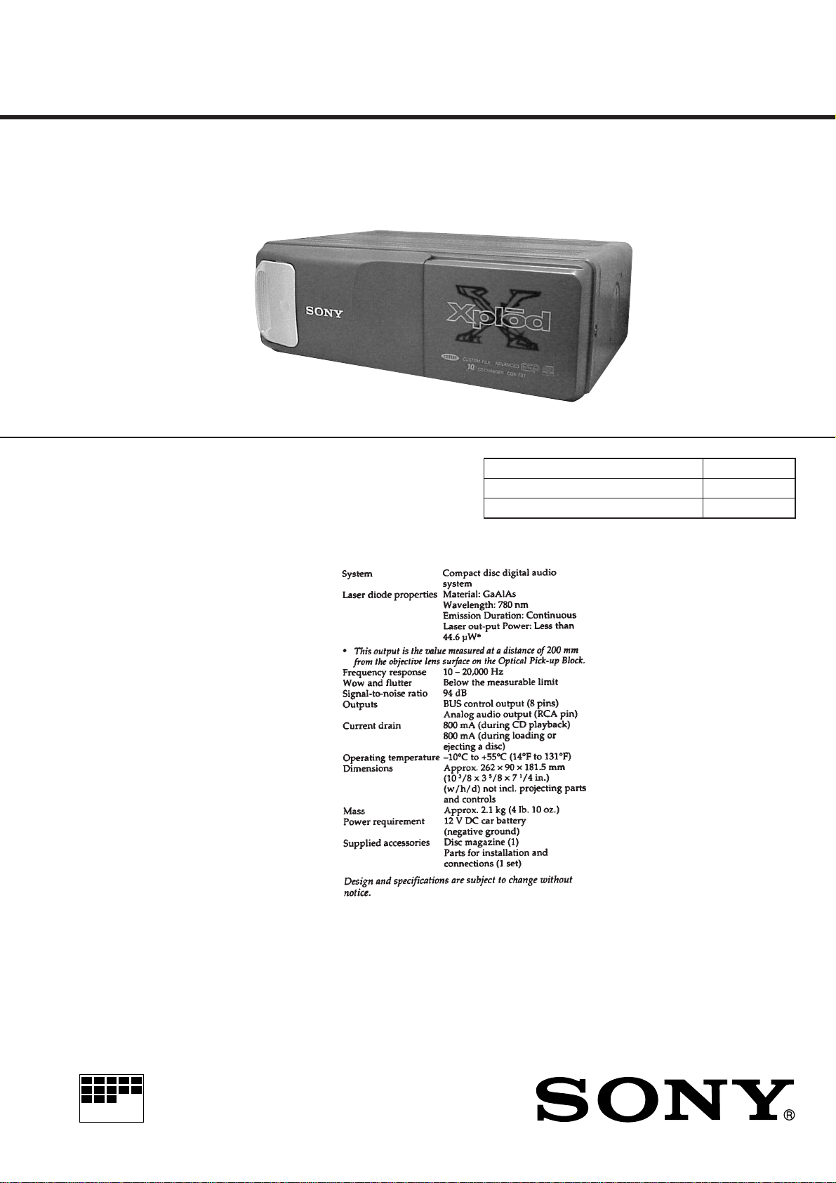
CDX-737
SERVICE MANUAL
SPECIFICATIONS
US Model
Canadian Model
AEP Model
UK Model
E Model
Model Name Using Similar Mechanism NEW
CD Drive Mechanism Type MG-250D-137
Optical Pick-up Name KSS-521A/J2N
MICROFILM
COMPACT DISC CHANGER

TABLE OF CONTENTS
1. SERVICING NOTES ................................................ 3
2. GENERAL ................................................................... 3
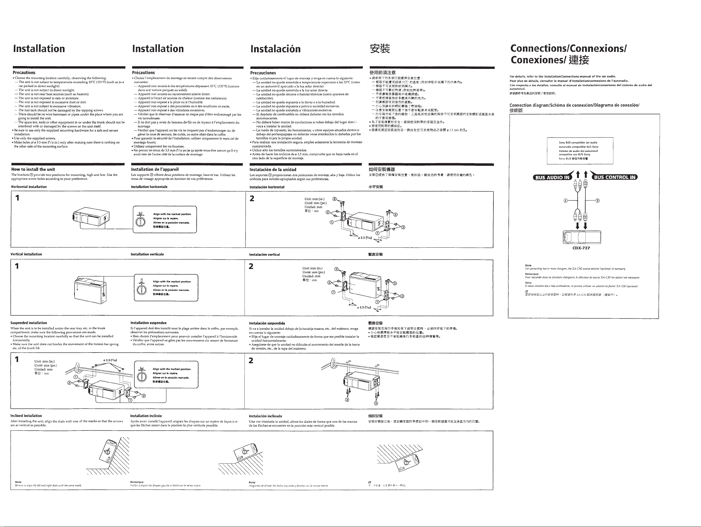
Installation....................................................................... 4
Connections ..................................................................... 4
3. DISASSEMBLY ......................................................... 5
4. MECHANISM DECK ASSEMBLY.................... 11
5. MECHANICAL ADJUSTMENTS....................... 13
6. ELECTRICAL ADJUSTMENTS......................... 14
7. DIAGRAMS
7-1. Block Diagram – SERVO Section – ............................... 16
7-2. Block Diagram – MAIN Section – ................................. 17
7-3. Block Diagram
– BUS CONTROL/POWER SUPPLY Section –........... 18
7-4. Note for Printed Wiring Boards and
Schematic Diagrams ....................................................... 19
7-5. Printed Wiring Boards – RF/SW Boards –..................... 20
7-6. Schematic Diagram – RF/SW Boards – ......................... 21
7-7. Printed Wiring Boards
– MAIN Board (Component Side) – .............................. 22
7-8. Printed Wiring Board
– MAIN Board (Conductor Side) – ................................ 23
7-9. Schematic Diagram – MAIN Board (1/2) – ................... 24
7-10. Schematic Diagram – MAIN Board (2/2) – ................... 25
7-11. Printed Wiring Boards – JACK Board – ........................ 26
7-12. Schematic Diagram – JACK Board – ............................. 26
7-13. IC Pin Function Description ........................................... 33
8. EXPLODED VIEWS ................................................ 36
9. ELECTRICAL PARTS LIST ............................... 41
SAFETY-RELATED COMPONENT WARNING!!
COMPONENTS IDENTIFIED BY MARK 0 OR DOTTED
LINE WITH MARK 0 ON THE SCHEMATIC DIAGRAMS
AND IN THE PARTS LIST ARE CRITICAL TO SAFE
OPERATION. REPLACE THESE COMPONENTS WITH
SONY PARTS WHOSE PART NUMBERS APPEAR AS
SHOWN IN THIS MANUAL OR IN SUPPLEMENTS PUBLISHED BY SONY.
ATTENTION AU COMPOSANT AYANT RAPPORT
À LA SÉCURITÉ!
LES COMPOSANTS IDENTIFIÉS P AR UNE MARQUE 0
SUR LES DIAGRAMMES SCHÉMATIQUES ET LA LISTE
DES PIÈCES SONT CRITIQUES POUR LA SÉCURITÉ
DE FONCTIONNEMENT. NE REMPLACER CES COMPOSANTS QUE PAR DES PIÈCES SONY DONT LES
NUMÉROS SONT DONNÉS DANS CE MANUEL OU
DANS LES SUPPLÉMENTS PUBLIÉS PAR SONY.
2
SECTION 1
y
SERVICING NOTES
SECTION 2
GENERAL
This section is extracted from
instruction manual.
NOTES ON HANDLING THE OPTICAL PICKUP BLOCK OR BASE UNIT
The laser diode in the optical pick-up block may suffer electrostatic breakdown because of the potential difference generated by
the charged electrostatic load, etc. on clothing and the human body .
During repair, pay attention to electrostatic breakdown and also
use the procedure in the printed matter which is included in the
repair parts.
The flexible board is easily damaged and should be handled with
care.
Laser Diode Properties
• Material: GaAlAs
• Wavelength: 780 nm
• Emission Duration: continuous
• Laser Output Power: less than 44.6 µW*
* This output is the value measured at a distance of 200 mm
from the objective lens surface on the Optical Pick-up Block.
CAUTION
Use of controls or adjustments or performance of procedures
other than those specified herein may result in hazardous radiation exposure.
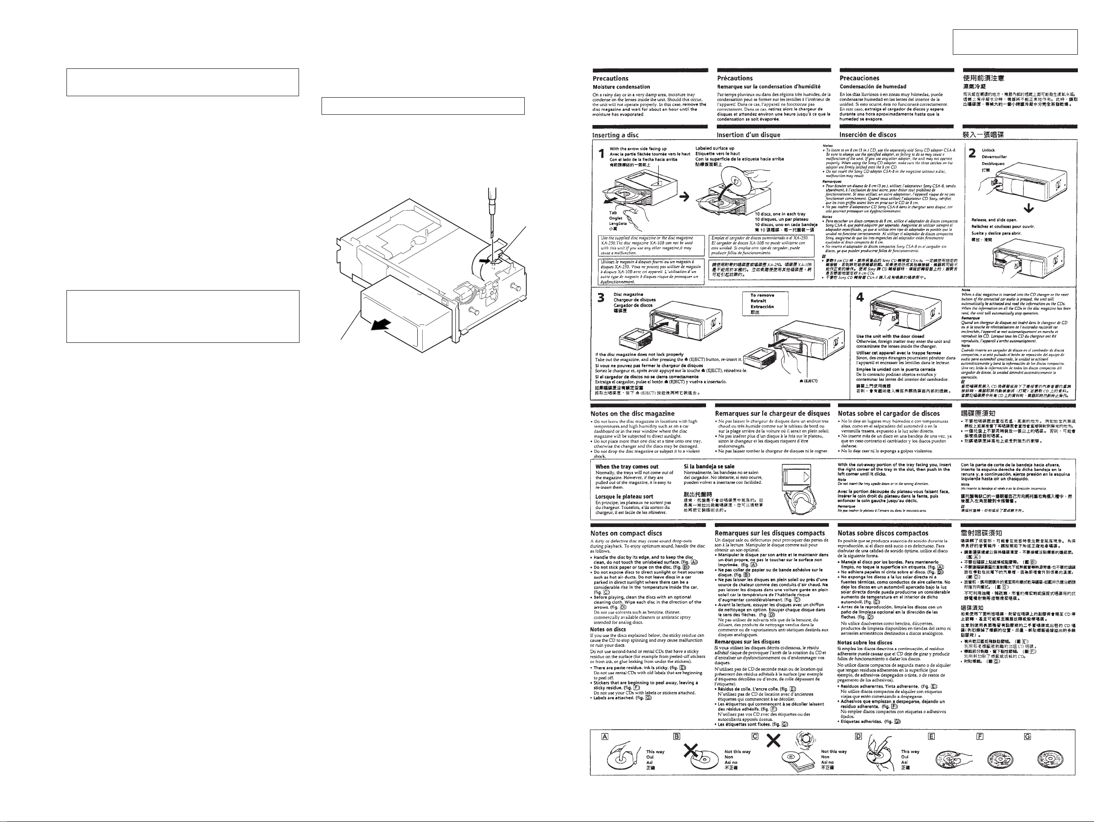
DISC MAGAZINE GETTING OUT PROCEDURE
ON THE POWER SUPPLY IS OFF
Remove the CASE (LOWER) assembly beforehand
1) Press the lever (ML) assy to arrow direction.
2) Removal the magazine assy.
Note: T ak e out the magazine only w hen the tray is completely within the
magazine. If the disk or tray is sticking out, turn on the power and
eject the magazine.
Lever (ML) ass’
Magazine ass’y
Flexible Circuit Board Repairing
• Keep the temperature of the soldering iron around 270 ˚C during repairing.
• Do not touch the soldering iron on the same conductor of the
circuit board (within 3 times).
• Be careful not to apply force on the conductor when soldering
or unsoldering.
Notes on chip component replacement
• Never reuse a disconnected chip component.
• Notice that the minus side of a tantalum capacitor may be damaged by heat.
33
44
SECTION 3
DISASSEMBLY
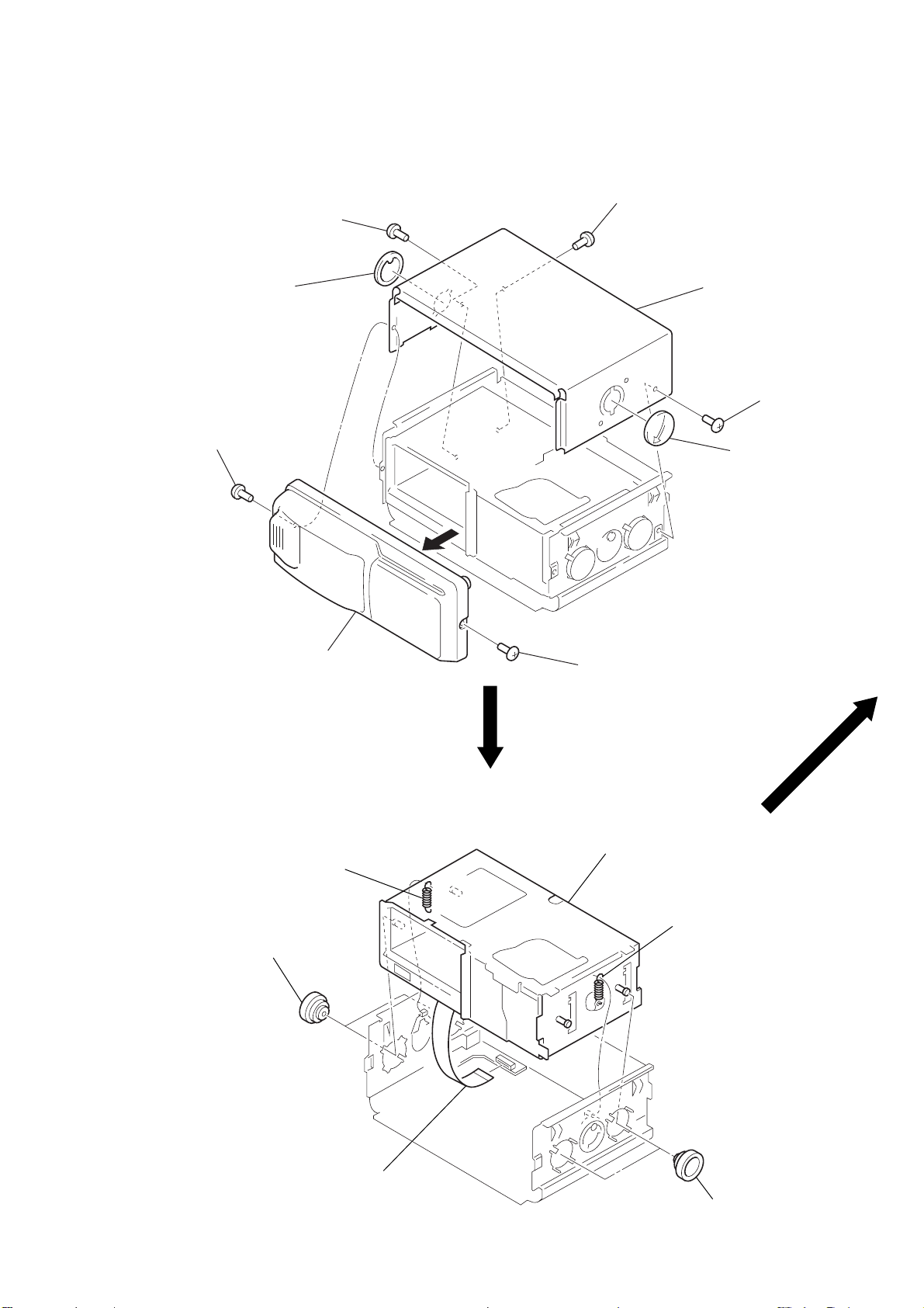
Note: Follow the disassembly procedure in the numerical order given.
COVER (UPPER T), FRONT PANEL ASS’Y
1
screw
(PTT2.6 × 6)
3
lever (FLT)
1
screw
(PTT2.6 × 6)
1
screw
(PTT2.6 × 6)
2
cover (upper T)
3
lever (FLT)
1
screw
(PTT2.6 × 6)
4
front panel (T) ass’y
MECHANISM DECK (MG-250D-137)
2
tension spring (FL)
1
two dampers (250)
1
screw
(PTT2.6 × 6)
4
mechanism deck (MG-250D-137)
2
tension spring (FL)
3
jack flexible board
(CNJ901)
1
two dampers (250)
5
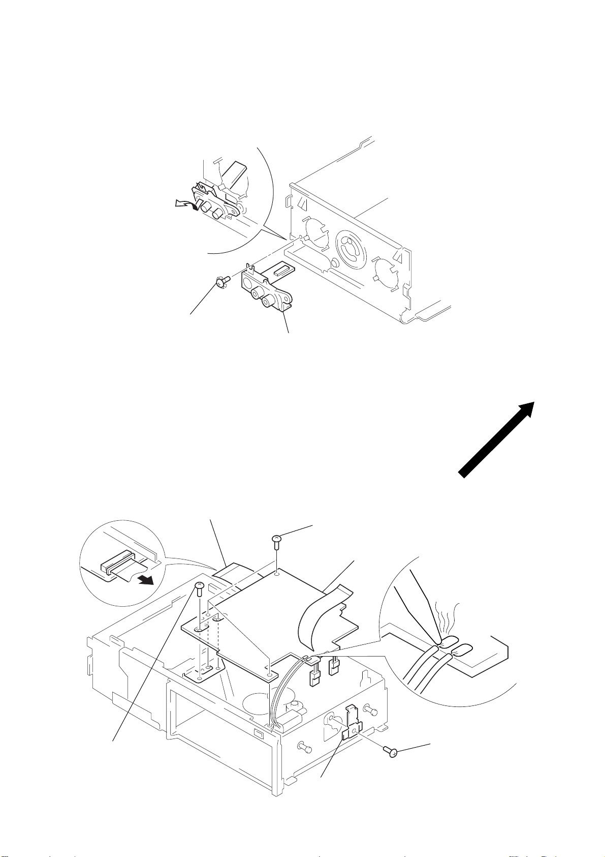
JACK BOARD
Remove the jack board
in the direction of the arrow.
1
ground point screw
(PTT2.6
×
6)
2
jack board
MAIN BOARD
5
two precision screws
(P1.7
×
2.5)
1
main flexible board
(CNJ12)
6
three screws (FP)
7
main board
2
Break the soldering
of motor (M104) lead.
3
screw
(PTT2
×
4)
4
heat sink
6
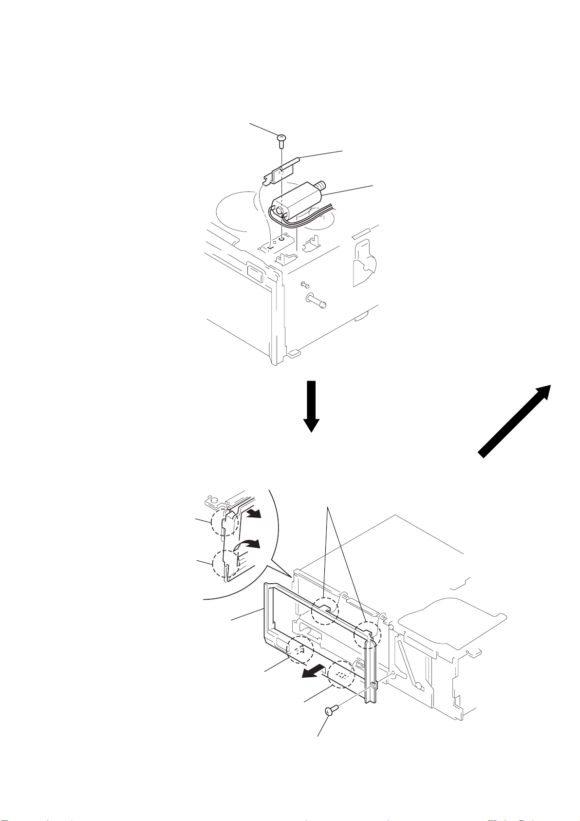
ELEVATOR MOTOR ASS’Y (M104)
1
screw
(PTT2
×
3)
2
bracket (EVM)
3
elevator motor ass’y
(M104)
ESCUTCHEON
2
Remove the claw
in the direction
of the arrow
4
Remove the ditch
in the direction
of the arrow
5
Remove the escutcheon
in the direction of the arrow
A
B
.
.
3
C
.
claw
B
A
4
C
ditch
two claws
3
1
screw
(M2
×
3)
7
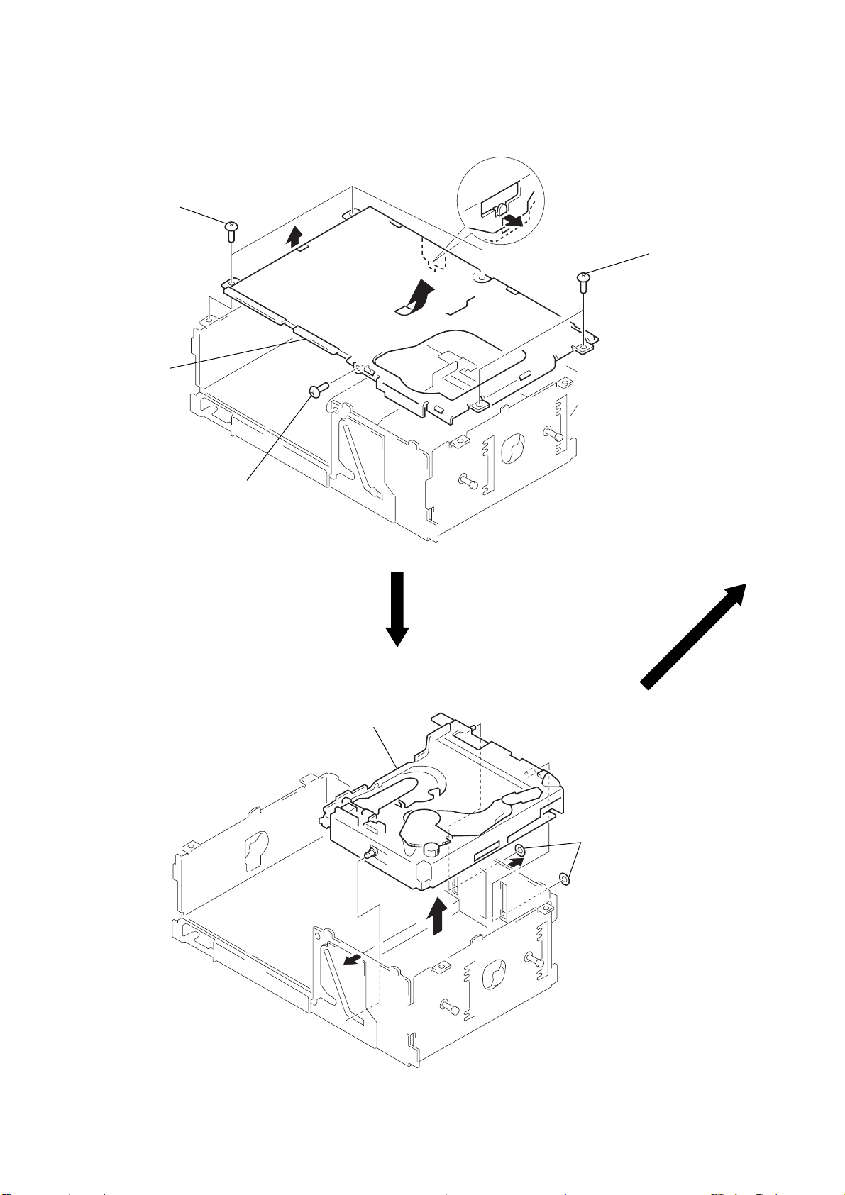
CASE (UPPER) ASS’Y
n
s
1
three screws
(PTT2 × 4)
Remove the case
4
(upper) ass’y
in the direction
of the arrow B.
1
screw
(PTT2 × 4)
2
B
A
3
Remove the edge in the directio
of the arrow A.
1
two screws
(PTT2 × 4)
CHASSIS ASS’Y
3
chassis ass’y
2
2
1
two polyethylene washer
8
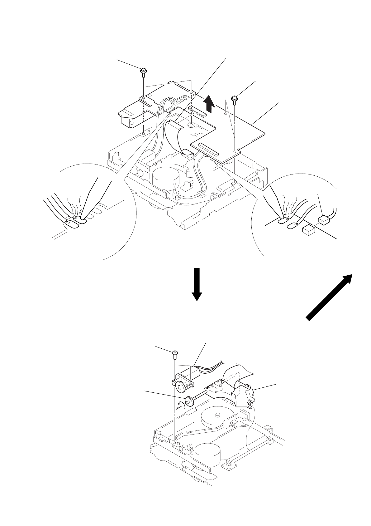
RF BOARD
3
two screws
(PS2 × 4)
1
OP flexible board
(CNJ11)
3
two screws
(PS2 × 4)
2
Break the soldering
of motor (M102) lead.
4
7
RF board
5
6
Break the soldering of lead.
connector
(CNP53)
SLED MOTOR ASS’Y (M102), OPTICAL PICK-UP (KSS-521A/J2N)
1
two screws
(ESCUTCHEON)
4
Turn at the direction of the
arrow, then remove
shaft (sled) ass’y
2
sled motor ass’y
(M102)
3
optical pick-up
(KSS-521A/J2N)
9
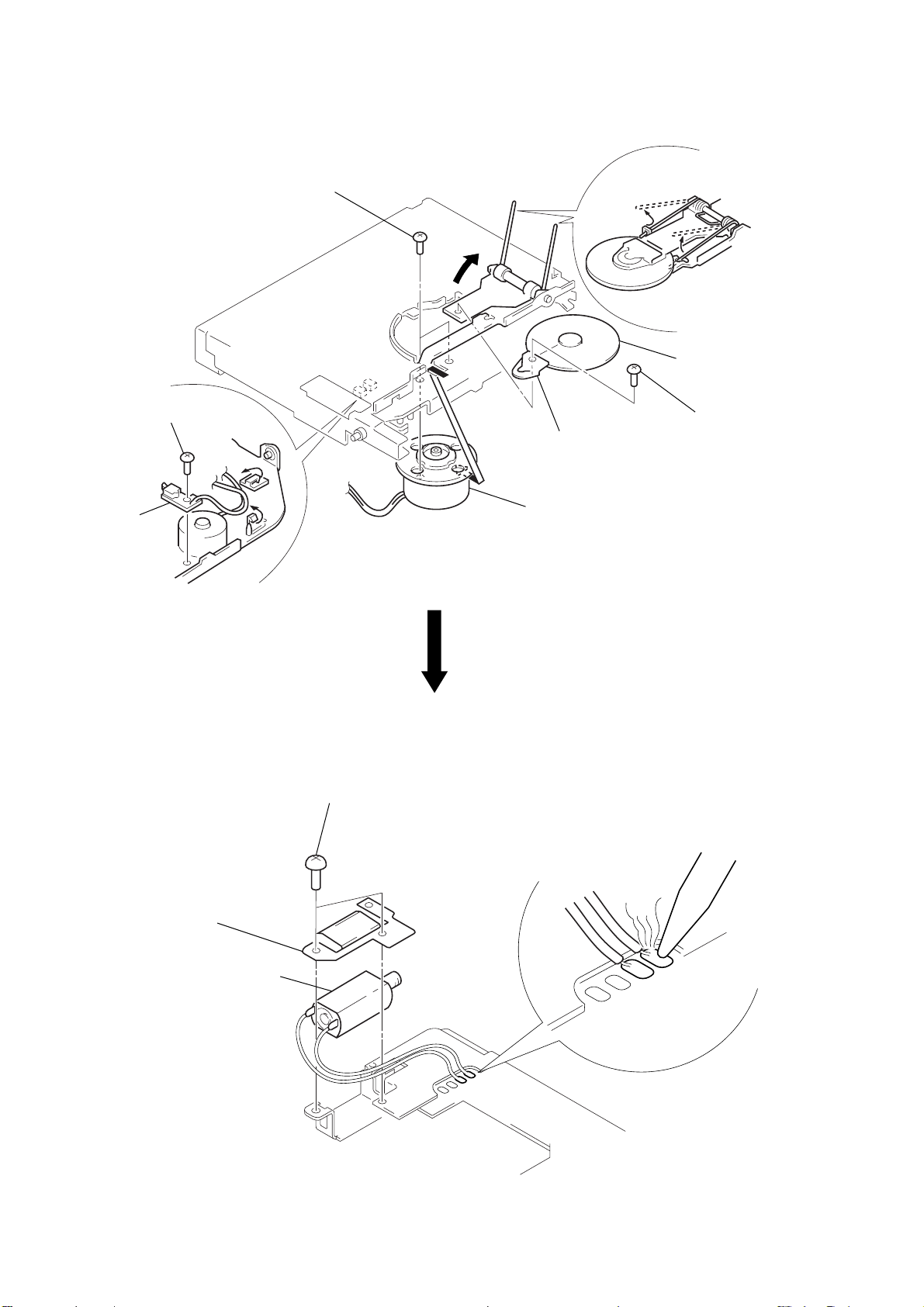
SW BOARD, SPINDLE MOTOR ASS’Y (M101)
)
8
two screws
×
2.2)
(P1.7
1
screw
×
2.2)
(P2
2
SW board
7
3
spring (chucking)
6
retainer (disc
4
screw
5
bracket (CP)
9
Remove the spindle motor ass’y (M101)
in the direction of the arrow.
(P2
×
2.2)
CHUCKING MOTOR ASS’Y (M103)
2
3
retainer (CHM)
4
chucking motor ass’y
(M103)
two screws (P2 × 2.5)
1
Break the soldering
of motor (M103) lead.
10
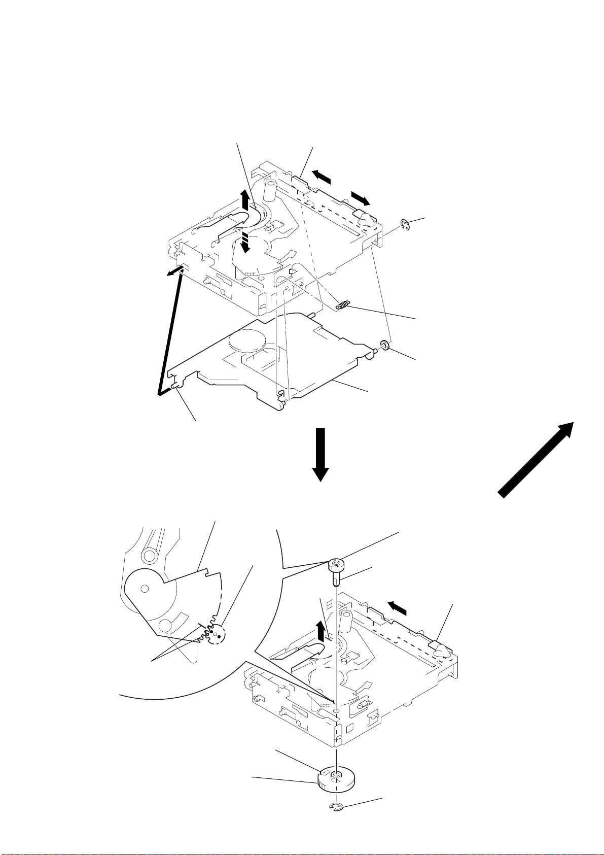
SECTION 4
)
gear (LOAD 2)
gear (LOMINI)
marking
Fig. A
chuck plate
2
Attach the gear (LOMINI) at the position
shown in Fig. A.
shaft (rotary prevention C)
1
Move the lever (LOCK 3)
fully in direction
B
to
move the chuck plate up.
B
4
stop ring 1.5 (E type)
3
Attach the gear (LOAD CAM) ass’y
with its facing inside.
slit
MECHANISM DECK ASSEMBLY
Note: Follow the assembly procedure in the numerical order given.
OPTICAL PICK-UP COMPLETE ASS’Y
1
Move the lever (LOCK 3) in direction A, and return it a little in
chuck plate
direction
down to the lower limit.
B
from the position where the chuck plate is moved
B
A
stop ring 2.0 (E type
4
5
tension spring (DH)
shaft (A)
GEAR (LOMINI) / (LOAD CAM) ASS’Y
3
optical pick-up complete ass’y
Note: Insert the shaft (A) first.
2
washer 2.5
11
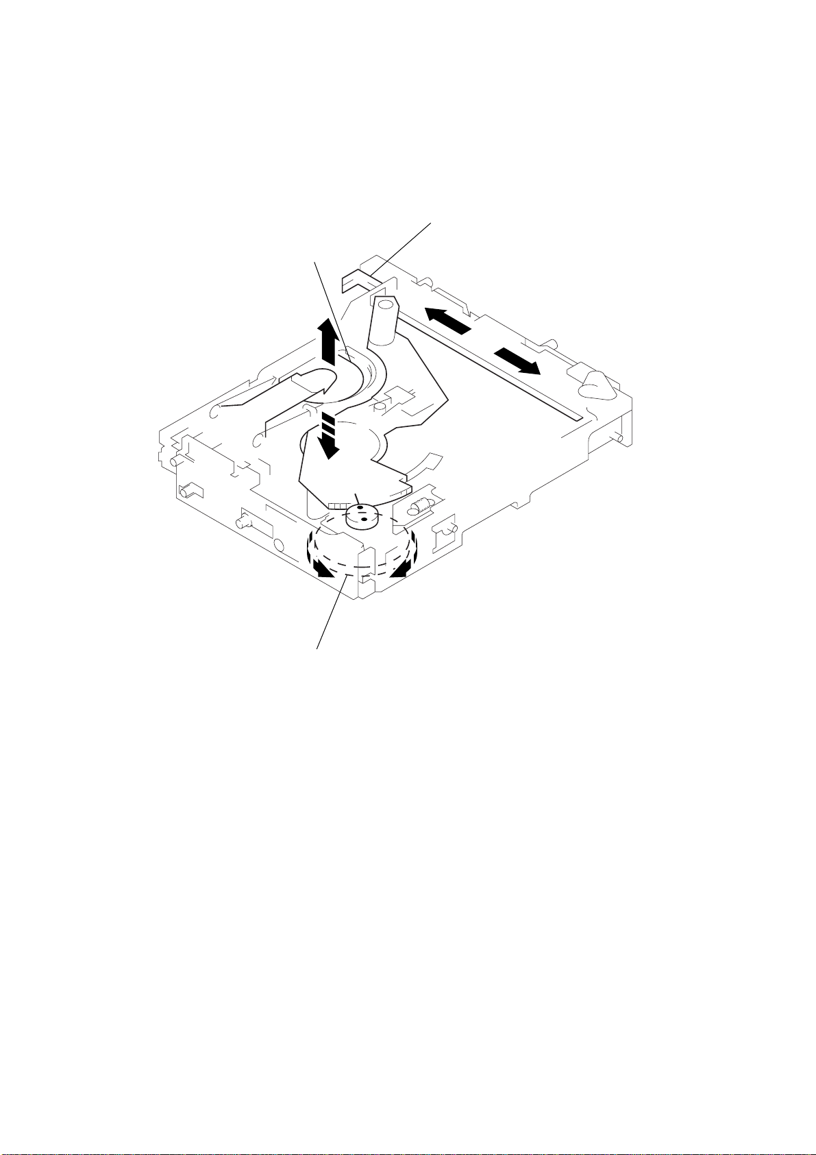
OPERATION CHECK
1
Confirm that the slider moves in direction C to move down
the chuck plate if the gear (LOAD CAM) is rotated in direction A or
the chuck plate moves up and the slider moves in direction D if the
gear is rotated in direction B.
chuck plate
slider
D
C
A
gear (LOAD CAM) ass’y
B
12
SECTION 5
5
MECHANICAL ADJUSTMENTS
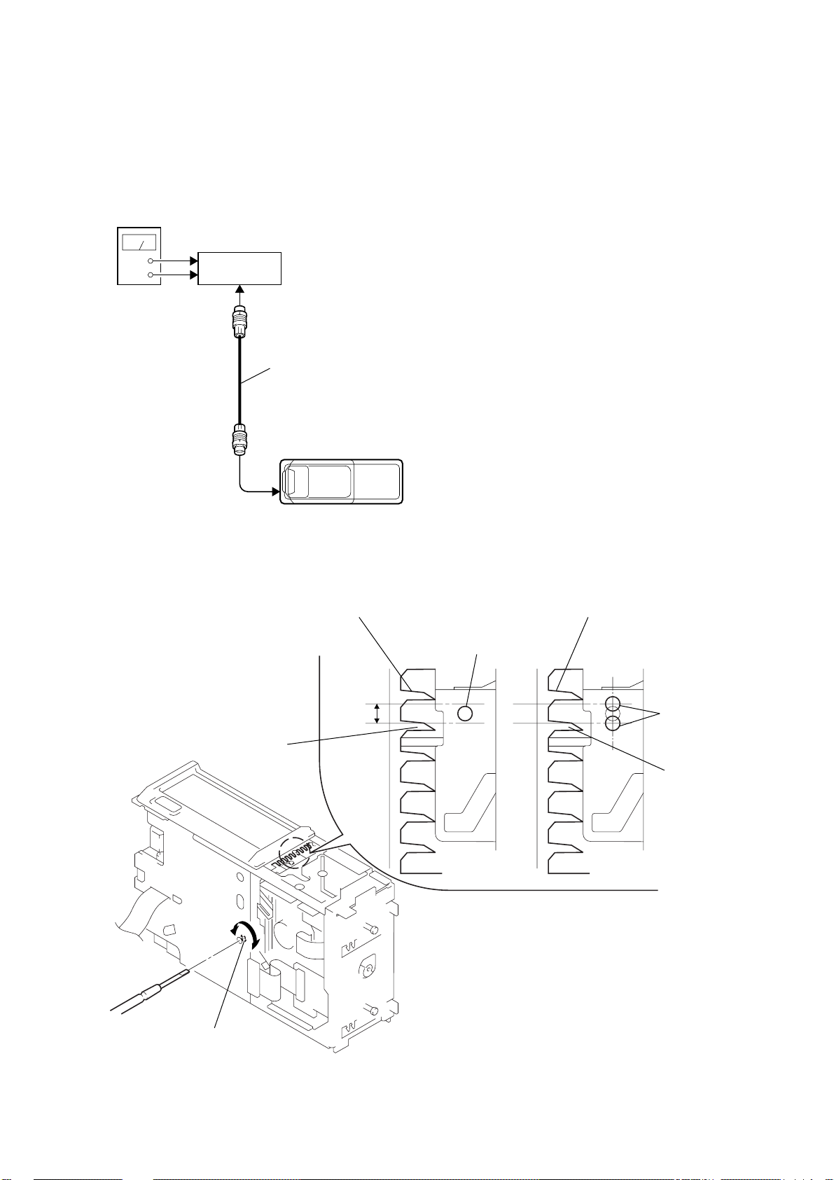
• Elevator Height (Address) Adjustment
Note: This adjustments is necessary when the system controller (IC201),
variable resistor (RV201), slider (R), slider (L), or chassis (ELV)
was replaced for any repair.
Connection:
power supply
master unit
+
GND
BUS cable
CDX-737
Adjustment Method:
1. Connect this set to the master unit (e.g. MDX-C7970/C7970R),
load a disc magazine, and place the set vertically as shown
below.
2. Connect the regulated power supply to the master unit, and
turn the power on.
3. Press the DISC button on the master unit and select DISC 5.
4. At this time, if the elevator shaft does not position between
comb teeth A and B at addresses 5 and 6 as shown below,
adjust the following.
5. Press repeatedly the DISC + and – buttons on the master unit
so that the elevator shaft mov es from address 6 to address 5, or
from 5 to 6. At this time, adjust RV201 on the main board so
that the elevator shaft positions smoothly between comb teeth
A and B.
6. Further, place the set horizontally and make same adjustment
as mentioned above.
7. After adjustment at addresses 5 to 6 is finished, check all operations from addresses 1 to 10 with the set placed vertically
and horizontally respectively to confirm that the elevator shaft
positions in a range between comb teeth A to B.
comb tooth at address 5
comb tooth at address 6
A
B
comb tooth at address 6
elevator shaft
A
B
OK NG
elevator shaft
comb tooth at address
RV201
13
SECTION 6
V
ELECTRICAL ADJUSTMENTS
Note:
1. Perform adjustments as given.
2. Power supply voltage: DC14.4 V (more than 3A).
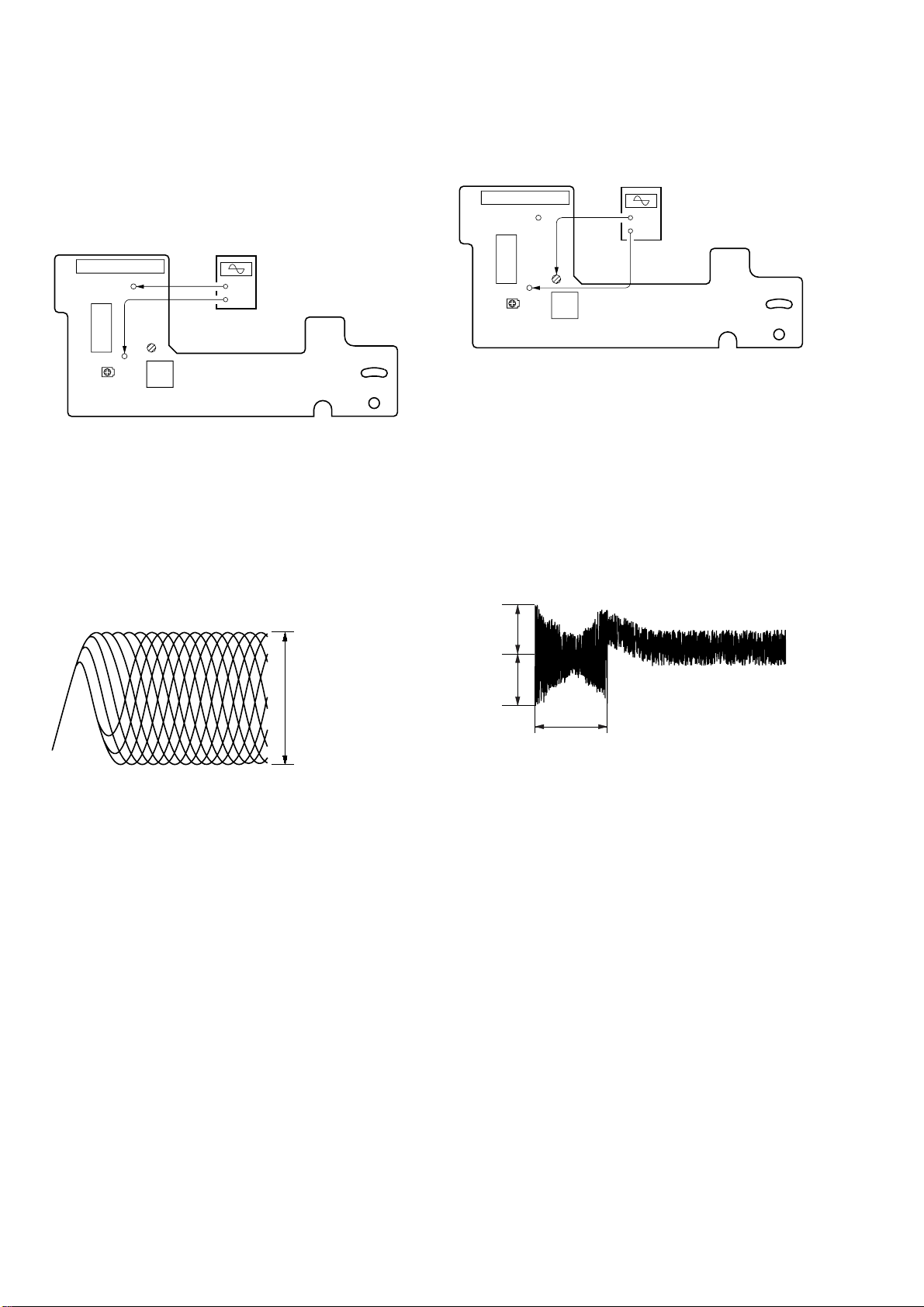
• FOCUS BIAS CHECK
– RF BOARD (Conductor Side) –
oscilloscope
CNJ12
TP (RF)
IC51
TP
(VC)
IC11
+
–
Procedure:
1. Connect the oscilloscope to TP (RF) and TP (VC) on the RF
board.
2. Put the set into play mode by loading the disc.
3. Confirm that oscilloscope waveform is clear and check RF
signal level is correct or not.
Note:
Clear RF signal waveform means that the shape “◊” can be clearly distinguished at the center of the waveform.
RF signal waveform
VOLT/DIV: 200 m
TIME/DIV: 500 ns
level: 1.4 ± 0.3 Vp-p
• TRACKING OFFSET CHECK
– RF BOARD (Conductor Side) –
oscilloscope
CNJ12
+
–
BP11
IC51
(TE)
TP
(VC)
IC11
Procedure:
1. Connect the oscilloscope to BP11 (TE) and TP (VC) on the
RF board.
2. Put the set into play mode by loading the disc.
3. Press the . AMS > button, and check the traverse w aveform*.
4. Confirm that the oscilloscope waveform is symmetrical on the
top and bottom in relation to 0 V dc, and check this level.
* Traverse waveform: This is the tracking error wave form appears
Traverse waveform
A
0 V
B
A=B
traverse waveform
(100 track jump waveform)
when crossing the track.
VOLT/DIV : 500 mV
TIME/DIV : 2 ms
Center : 0 V
14
