

Page 1
CDX-715
SERVICE MANUAL
SPECIFICATIONS
System Compact disc digital audio system
Laser diode properties Material: GaAlAs
Wavelength: 780 nm
Emission Duration: Continuous
Laser out-put Power: Less than 44.6 µW*
* This output is the value measured at a
distance of 200 mm from the objective lens
surface on the Optical Pick-up Block.
Frequency response 10 – 20,000 Hz
Wow and flutter Below the measurable limit
Signal-to-noise ratio 94 dB
Outputs BUS control output (8 pins)
Analog audio output (RCA pin)
US Model
Canadian Model
AEP Model
UK Model
E Model
Model Name Using Similar Mechanism NEW
CD Drive Mechanism Type MG-250B-137
Optical Pick-up Name KSS-521A/J2N
Currnet drain 800 mA (during CD playback)
800 mA (during loading or ejecting a disc)
Operating temperature –10˚C to +55˚C (14˚F to 131˚F)
Dimensions Approx. 262 × 90 × 181.5 mm
(10 3/8 × 3 5/8 × 7 1/4 in.)
(w/h/d)
not incl. projecting parts and controls
Mass Approx. 2.1 kg (4 lb. 10 oz.)
Power requirement 12 V DC car battery (negative ground)
Supplied accessories Disc magazine (1)
Parts for installation and connections (1 set)
Design and specifications subject to change without notice.
MICROFILM
COMPACT DISC CHANGER
Page 2
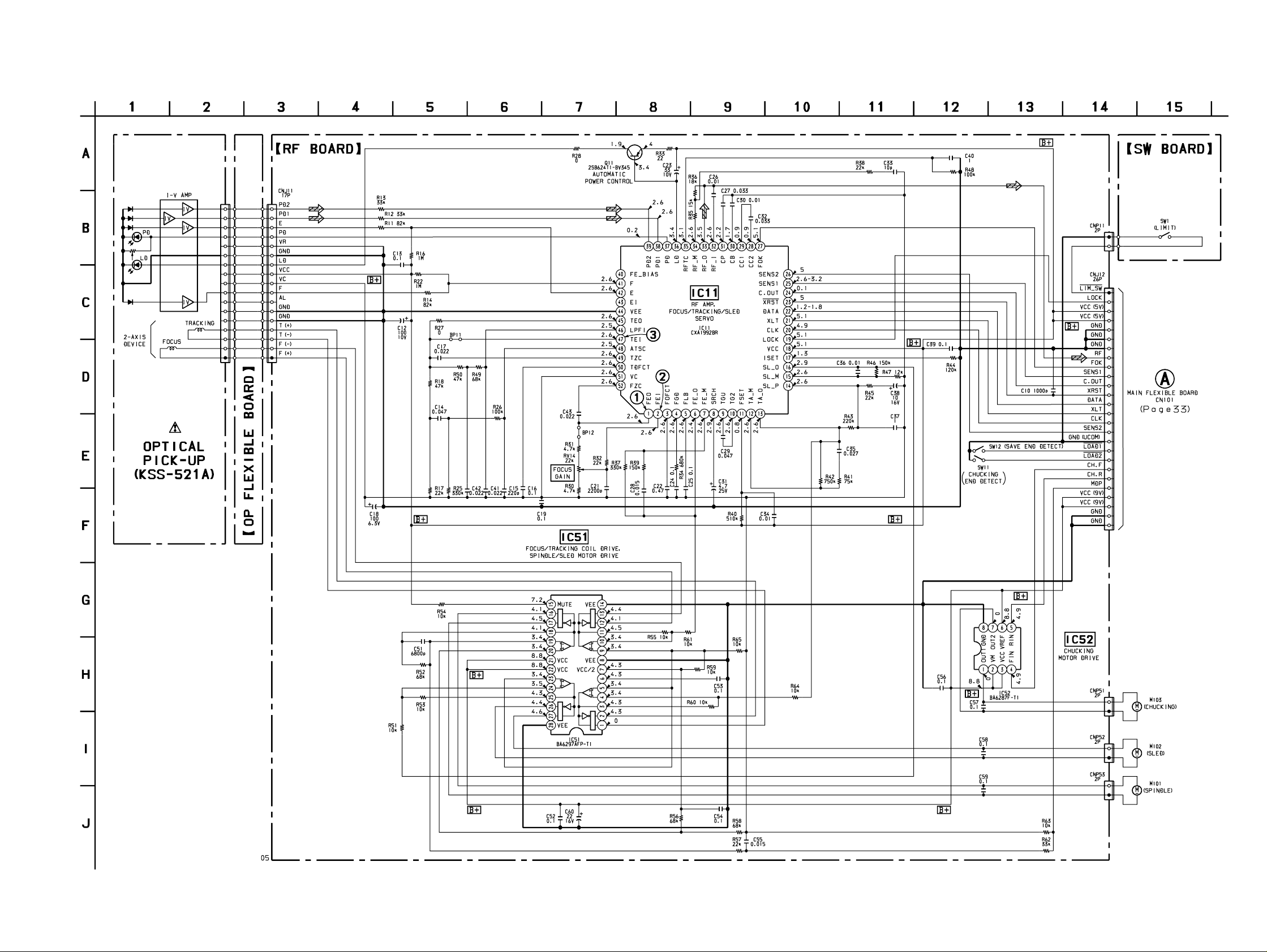
7-3. SCHEMATIC DIAGRAM – RF Section – • See page 25 for Note on Schematic Diagram. • See page 39 for Waveforms. • See page 41 and 42 for IC Block Diagrams.
CDX-715
– 27 – – 28 –
Page 3
CDX-715
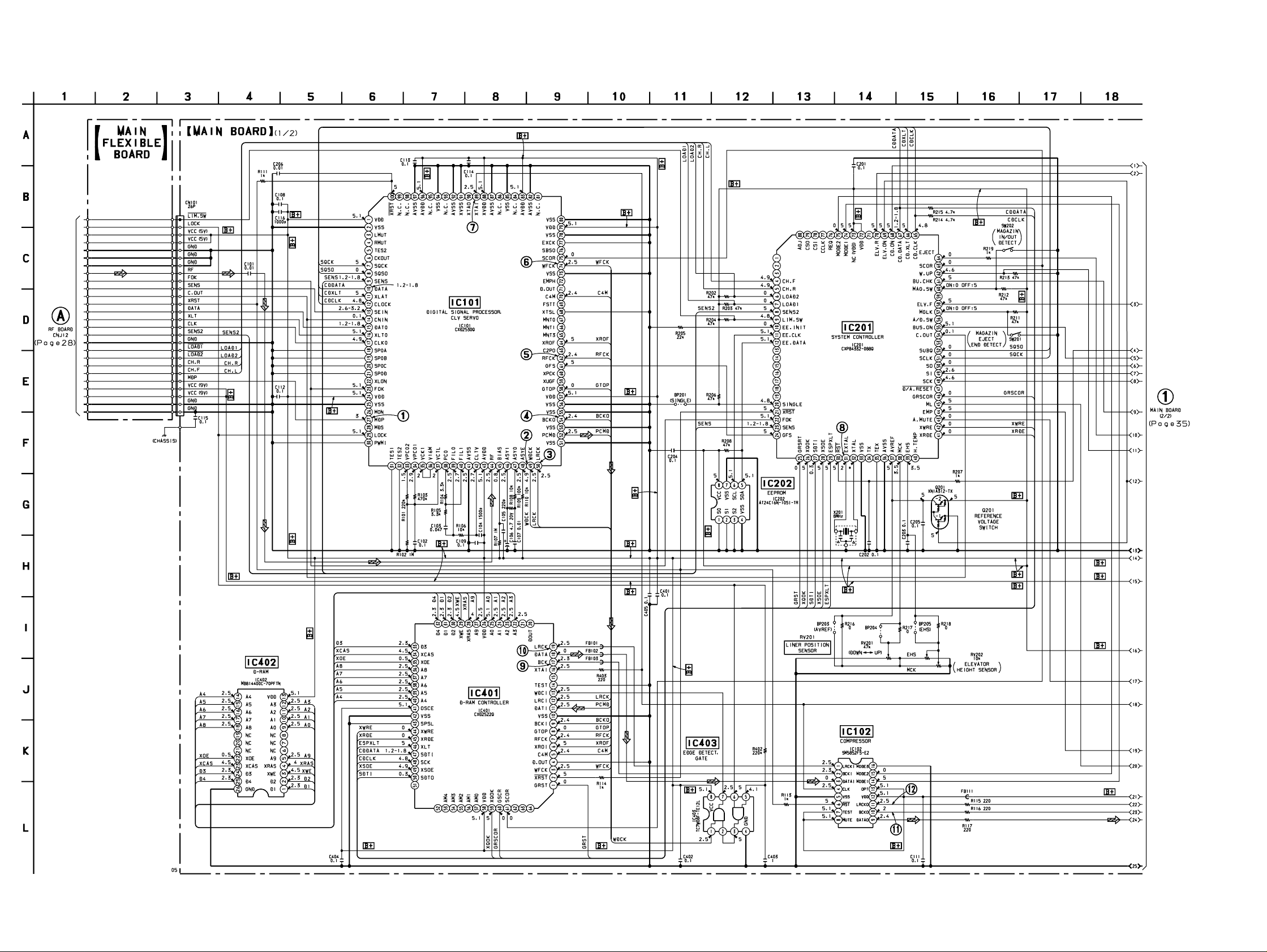
7-5. SCHEMATIC DIAGRAM – MAIN Section – MAIN Board (1/2)
• See page 39 and 40 for Waveforms. • See page 42 to 44 for IC Block Diagrams. • See page 45 and 46 for IC Pin Function Description. • See page 36 for Note on Schematic Diagram. • See page 29 to 32 for Printed Wiring Board.
– 33 – – 34 –
Page 4
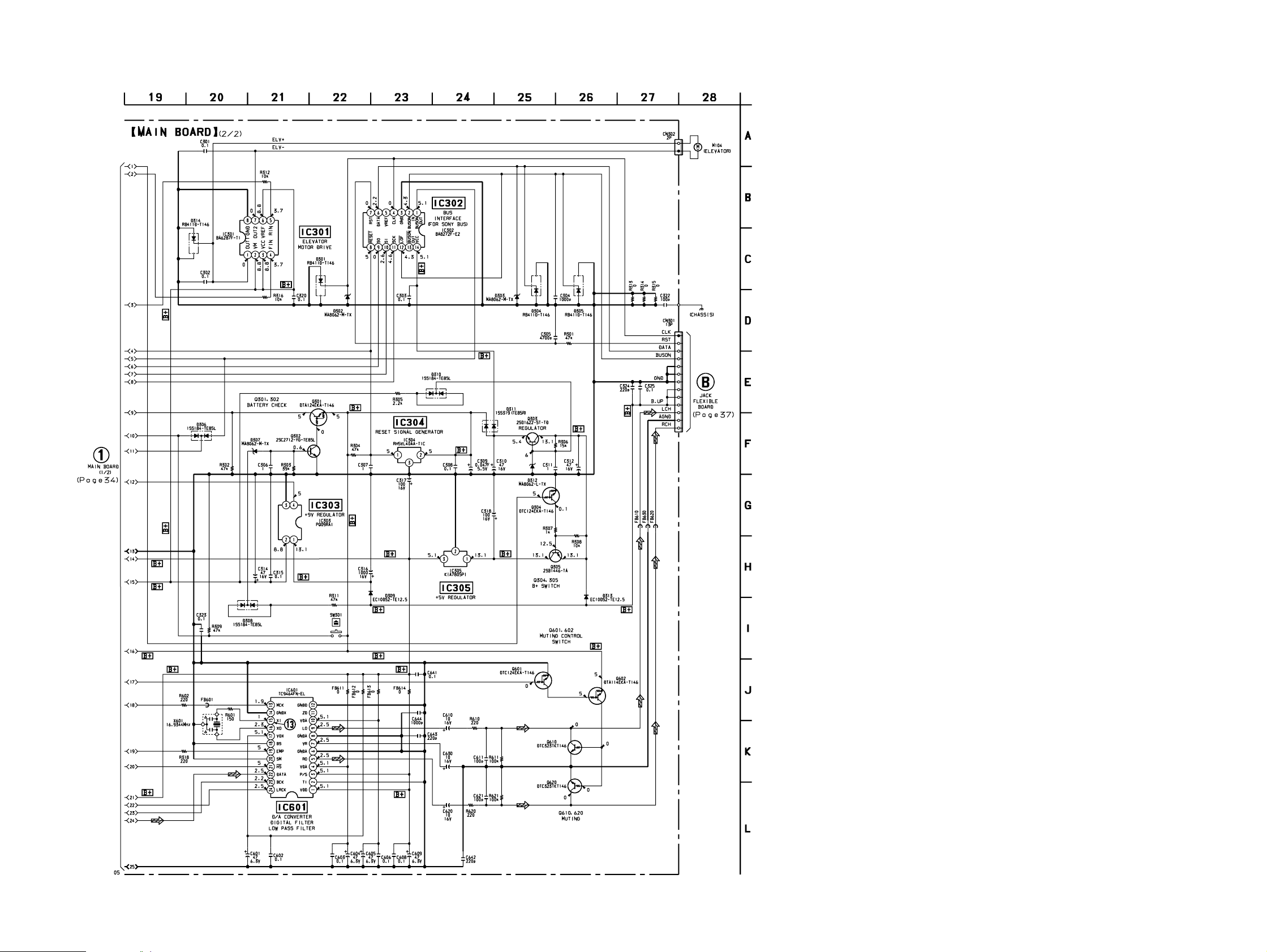
– MAIN Section – MAIN Board (2/2)
• See page 40 for Waveforms. • See page 43 and 44 for IC Block Diagrams. • See page 29 to 32 for Printed Wiring Board.
CDX-715
Note on Schematic Diagram:
• All capacitors are in µF unless otherwise noted. pF: µµF
50 WV or less are not indicated except for electrolytics
and tantalums.
• All resistors are in Ω and 1/
specified.
¢
•
• U : B+ Line.
• H : adjustment for repair.
• Power v oltage is dc 14.4 V and f ed with regulated dc power
• Voltages and waveforms are dc with respect to ground
• Voltages are tak en with a V OM (Input impedance 10 MΩ).
• Waveforms are taken with a oscilloscope.
• Circled numbers refer to waveforms.
• Signal path.
: internal component.
supply from CD changer controller.
under no-signal conditions.
no mark : PLAY
Voltage variations may be noted due to normal production tolerances.
Voltage variations may be noted due to normal production tolerances.
J : CD
: Impossible to measure
∗
4
W or less unless otherwise
– 35 – – 36 –
Page 5

CDX-715
7-6. PRINTED WIRING BOARD – JACK Section – 7-7. SCHEMATIC DIAGRAM – JACK Section –
Note on Schematic Diagram:
• All capacitors are in µF unless otherwise noted. pF: µµF
50 WV or less are not indicated except for electrolytics
and tantalums.
• All resistors are in Ω and 1/
specified.
• C : panel designation.
• U : B+ Line.
• Signal path.
J : CD
• Abbreviation
G : German model.
4
W or less unless otherwise
Note on Printed Wiring Board:
• X : parts extracted from the component side.
• p : parts mounted on the conductor side.
r
•
• b : Pattern from the side which enables seeing.
(The other layers' patterns are not indicated.)
Caution:
Pattern face side: Parts on the pattern face side seen from
(Conductor Side) the pattern face are indicated.
Parts face side: Parts on the parts face side seen from
(Component Side) the parts face are indicated.
• Abbreviation
: Through hole.
G : German model.
– 37 – – 38 –
Page 6

• Wavef orms
6 Vp-p
472 ns
– RF Board –
1 IC11 1 (FEO)
500 mV/DIV, 500 nsec/DIV
2 IC11 2 (FEI)
50 mV/DIV, 1 µsec/DIV
1.4 ±0.3 Vp-p
– MAIN Board (1/2) –
1 IC101 @¶ MDP
3.8
2 IC101 $ª WDCK
2.5 Vp-p
µ
s
3 IC11 $¶ (TEI)
200 mV/DIV, 500 µsec/DIV
Approx. 110 mVp-p
Approx. 280 mVp-p
5 Vp-p
11.4 µs
3 IC101 %º LRCK
5 Vp-p
22.5 µs
4 IC101 %¢ BCKO
5 IC101 ^™ RFCK
5 Vp-p
136.5 µs
– 39 –
Page 7

6 IC101 &¢ WFCK
!¡ IC102 0 BCKO
137 µs
7 IC101 *ª XTAI
59 ns
8 IC201 #¡ EXTAL
5 Vp-p
4.5 Vp-p
3.3 Vp-p
5.3 Vp-p
472 ns
!™ IC102 !¡ LRCKO
5.3 Vp-p
22.6 µs
– MAIN Board (2/2) –
!£ IC601 !∞ XI
124.5 ns
9 IC401 !¶ BCK
472 ns
0 IC401 !ª LRCK
2.9 Vp-p
59 ns
5.9 Vp-p
5.8 Vp-p
22.8 µs
– 40 –
Page 8

• IC Block Diagrams
IC11 CXA1992BR (RF BOARD)
FE_BIAS
LPFI
ATSC
TDFCT
VEE
TEO
TZC
FZC
PD2
PD1
PD
LD
RFTC
RF_M
RF_O
RF_I
CP
CB
CC1
CC2
FOK
27282930313233343536373839
VEE
+
–
+
–
–
+
RF SUMMING
AMP
FOH
FOL
TGH
TGL
BALH
BALL
ATSC
TZC
FZC
+
–
–
+
–
+
–
–
+
VEE
MIRR
VCC
–
+
–
–
+
+
–
–
+
VEE
LEVEL S
VCC
–
+
FOK
LDON
LPCL
LPC
TGFL
IIL DATA REGISTER
INPUT SHIFT REGISTER
ADDRESS DECODER
SENS SELECTOR
OUTPUT DECODER
DFCTO
IFB1-6
FS1-4 TG1-2 TM1-7 PS1-4
BAL1-4
TOG1-4
+
SENS2
26
+
–
IIL
↓
VCC
–
+
–
VEE
+
–
+
TTL
DFCT
+
IIL
↓
MIRR
TTL
DFCT1
CC1
TTL
↓
IIL
VCC
ISET
VCC VCC
SENS1
25
C. OUT
24
XRST
23
DATA
22
XLT
21
CLK
20
LOCK
19
VCC
18
ISET
17
SL_O
16
TM4 TM6
SL_M
VCC
FS1
FS2
Charge
up
TG2
TM7
FSET
TM3
TM5
VEEVEE
–
+
15
–
SL_P
14
+
TM2
–
+
PD2 IV
AMP
40
F
41
E
42
–
+
–
+
F IV AMP
PD1 IV
AMP
–
+
VCC
+
APC
+
–
–
+
–
VEE
LASER POWER CONTROL
VCC
FE AMP
–
+
E IV AMP
+
43
EI
BAL1
BAL2
BAL3
BAL4
VEE
44
TOG4
TOG3
TOG2
TOG1
+
TGFL
–
VEE
45
+
–
E-F BALANCE
VCC
VEE
WINDOW COMP.
+
–
DFCT
TM1
–
+
–
+
+
–
ATSC
WINDOW
COMP.
–
+
46
47
TEI
48
49
TZC COMP.
50
51
VC
+
–
VCC
52
+
–
IFB1
+
–
IFB2
IFB4
IFB3
+
–
TRK. GAIN
WINDOW COMP.
+
–
TG1
–
IFB5
IFB6
FOCUS
PHASE COMPENSATION
FO. BIAS
WINDOW
COMP.
TRACKING
PHASE COMPENSATION
DFCT
FZC COMP.
FS4
VEE
1
2 3
FEO
FEI
4
FDFCT
5 6 7 8 9 10
FGD
FLB
FE_O
FE_M
SRCH
TGU
TG2
FSET
TA_M
131211
TA_O
– 41 –
Page 9

IC52, 301 BA6287F (RF BOARD, MAIN BOARD)
1
OUT1
VM
VCC
FIN
2
DRIVER DRIVER
TSD
3
POWER
SAVE
4
CONTROL LOGIC
8
GND
7
OUT2
6
VREF
5
RIN
IC101 CXD2530Q (MAIN BOARD)
TES6
VDD
VSS
EXCK
SBSO
SCOR
WFCK
TES5
EMPH
DOUT
C4M
FSTT
XTSL
MNT0
MNT1
66 65 64
67
ERROR
CORRECTOR
16K RAM
SERVO
AUTO
MNT3
VSS
VDD
TES7
VSS
XVDD
XTAI
XTAO
XVSS
VSS
TES8
VDD
VSS
XRST
79 78
80
NC
81
82
83
NC
84
85
86
NC
87
88
89
90
91
92
NC
93
94
NC
95
96
97
98
NC
NC
99
100
TIMING
LOGIC
76 75 74
77
73 72
DEMODULATOR
SUB CODE
PROCESSOR
CPU
INTERFACE
EFM
69 68
70
71
SEQUENCER
XROF
C2PO
63 62 61
RFCK
GFS
XPCK
59 58
60
D / A
INTERFACE
DIGITAL OUT
DIGITAL CLV
XUGF
GTOP
57
VDD
VSS
56 55 54
TES4
BCK
TES3
53 52 51
ASYMMETRY
CORRECTOR
DIGITAL
PLL
CLOCK
GENERATOR
PCMD
OSC
TES9
LRCK
50
49
WDCK
48
ASYE
47
ASYO
ASYI
46
BIAS
45
RF
44
AVDD
43
42
CLTV
AVSS
41
40
FILI
39
FILO
PCO
38
VCTL
37
V16M
36
35
VCKI
34
VPCO1
33
VPCO2
32
TES1
31
TES0
1 234
VSS
VDD
56789 10
TES2
LMUT
RMUT
CKOUT
SQCK
SQSO
SENS
11
DATA
XLAT
12 13
CLOK
14
SEIN
15 16 17
CNIN
IC102 SM5852FS-E2 (MAIN BOARD)
LRCI
BCKI
CLK
VSS
RSTN
TESTN
MUTEN
1
2
3
DI
4
5
6
7
8
INPUT
INTERFACE
SYSTEM
CLOCK
SEQUENTIAL
CONTROL
MUTE
CONTROL
DIGITAL
SIGNAL
PROCESSOR
OUTPUT
INTERFACE
MODE
CONTROL
DATO
XLTO
18 19 20
CLKO
SPOA
16
15
14
13
12
11
10
9
SPOB
DB/DS
MOD2
MOD1
OPT
VDD
LRCO
BCKO
DOUT
21
SPOC
22 23
SPOD
24
FOK
XLON
– 42 –
25 26 27
VSS
VDD
MON
28 29 30
MDP
MDS
LOCK
PWMI
Page 10

IC202 AT24C16N-10SI-TR (MAIN BOARD) IC302 BA8272F-E2 (MAIN BOARD)
VCC
8
NC
SCL
D OUT
SDA
8
7
6
5
VCC
2 3
1
BUS ON OUT
BUS ON
LINK OFF
GND
BUS ON IN
CLK OUT
DATA OUT
5 6 7
4
VREF
BUS CLK
BUS DATA
DATA IN
RESET
891014 13 12 11
RESET
SWITCH
BUS RESET
START CYCLE
START/
STOP
LOGIC
CONTROL
R/W
LOGIC
LOAD
WORD
ADDRESS
COUNTER
INC
SLAVE ADDRESS
REGISTER &
A0
1
A1
2
A2
3
4
VSS
COMPARATOR
DEVICE
ADDRESS
BITS
D OUT
ACK
H.V. GENERATOR
TIMING & CONTROL
4
CK
D IN
EEPROM
128 x 16 x 8
16
Y
DECODER
8
DATA
REGISTER
X
DECODER
416
IC401 CXD2522Q (MAIN BOARD)
XLT
WRITE
BASE
RFCK
XRDE
GTOP
XWRE
43444546
SPSL
VWA
BCKI
DSP
I/F
VSS
DATI
XWIH
AM4
AM3
AM2
AM1
AM0
VDD
XQOK
GSCR
SCOR
XEMP
SDTO
XSOE
SCK
CPU I/F
ADDRESS MONITOR
READ
BASE
COUNTER
DATA
LINKING
DIN
C4M
WFCK
SDTI
COUNTER
XROI
51 50 49 48 47
52
53
54
55
56
57
58
59
60
61
NC
62
NC
63
NC
64
CONTROL
2 345 6 7 8 9 10
1
XRST
GRST
VSS
LRCI
WDCI
OSCE
TEST
XTAO
A5
A4
XTAI
A7
A6
DRAM
I/F
SELECTOR
TIMING
GEN.
DAC
I/F
BCK
DATA
191817161514131211
A8
LRCK
XOE
DIGITAL
OUT
XCAS
33343536373839404142
D2
D3
32
D0
31
D1
30
XWE
29
XRAS
28
A9
27
26
VDD
A0
25
24
A1
A2
23
A3
22
21
C176
DOUT
20
– 43 –
Page 11

IC402 MB814400C-70PFTN
CLOCK OSC
COLUMN DECODER
SENSE REFRESH AMP
INPUT/OUTPUT
CONTROL SWITCH
MEMORY CELL
ROW DECODER
XWE
XRAS
VDD
1
D1
2
D2
3
4
A9
5
6
NC
7
NC
8
NC
9
A0
A1
10
11
A2
12
A3
13
A0–A9
A0–A9
ADDRESS BUFFER
IC601 TC9464FN-EL (MAIN BOARD)
INPUT
BUFFER
BUFFER
OUTPUT
GND
26
D4
25
D3
24
XCAS
23
XOE
22
NC
21
NC
20
19
NC
A8
18
17
A7
A6
16
15
A5
A4
14
LRCK
BCK
DATA
INTERFACE
CIRCUIT
DIGITAL FILTER CIRCUIT
ATTENUATOR OPERATIONAL CIRCUIT
DEEMPHASIS FILTER CIRCUIT
D-∆ MODULATION CIRCUIT
TEST
CIRCUIT
2 3
1
T1
VDD
P/S
ATT
HS
(SM)
20 19 18 17 16 15 14 13
21222324
MICROCOMPUTER
INTERFACE
CIRCUIT
OUTPUT
CIRCUIT
ANALOG
FILTER
5 6 7 8 9 10
4
RO
VDA
SH
(EMP)
GNDA
(BS)
VR
LA
VDXXOXI
TIMING
GENERATOR
OUTPUT
CIRCUIT
ANALOG
FILTER
GNDA
OSC
GNDX
MCK
1211
LO
VDA
ZD
GNDD
– 44 –
Page 12

7-8. IC PIN FUNCTION DESCRIPTION
• MAIN BOARD IC201 CXP84332-088Q (SYSTEM CONTROLLER)
Pin No. Pin Name I/O Function
1 to 3 — O Not used (open)
4 CH.F O Motor drive signal (load chucking direction) output to the chucking motor drive (IC52) *1
5 CH.R O Motor drive signal (save direction) output to the chucking motor drive (IC52) *1
6 LOAD2 I
Chucking end detect switch (SW11) input
“L”: When completion of the disc chucking operation
7 LOAD1 I
8 SENS2 I Internal status signal (sense signal) input from the CXA1992AR (IC11)
9 LIM.SW I
10 EE.INIT I Initialize signal input for the EEPROM (IC202) “H”: format Fixed at “L” in this set
11 EE.CLK O Serial data transfer clock signal output to the EEPROM (IC202)
12 EE.DATA I/O Two-way data bus with the EEPROM (IC202)
13 to 19 — O Not used (open)
20 SINGLE I
21 XRST O
22 FOK I Focus OK signal input from the CXA1992AR (IC11) “L”: NG, “H”: OK
23 SENS I Internal status signal (sense signal) input from the CXD2530Q (IC101)
24 GFS I Guard frame sync signal input from the CXD2530Q (IC101) “L”: NG, “H”: OK
25 GRSRT O Reset signal output to the CXD2522Q (IC401) “L”: reset
26 XQOK O Subcode Q OK pulse signal output to the CXD2522Q (IC401) “L” active
27 SDTI I ESP status signal input from the CXD2522Q (IC401)
28 XSOE O ESP status read enable signal output to the CXD2522Q (IC401) “L” active
29 ESPXLT O ESP latch pulse signal output to the CXD2522Q (IC401) “L” active
Save end detect switch (SW12) input
“L”: When completion of the disc chucking operation
Sled limit in detect switch (SW1) input
“L”: When the optical pick-up is inner position
Setting terminal for the single disc/multiple discs mode
“L”: single mode, “H”: multiple discs mode (fixed at “H”)
System reset signal output to the CXA1992AR (IC11), CXD2530Q (IC101) and SM5852FS
(IC102) “L”: reset
System reset signal input from the SONY bus interface (IC302) and reset signal generator
30 RST I
31 EXTAL I Main system clock input terminal (8 MHz)
32 XTAL O Main system clock output terminal (8 MHz)
33 VSS — Ground terminal
34 TX O Sub system clock output terminal Not used (open)
35 TEX I Sub system clock input terminal Not used (fixed at “L”)
36 AVSS — Ground terminal (for A/D converter)
37 AVREF I Reference voltage (+5V) input terminal (for A/D converter)
38 MCK I
39 EHS I Elevator height position detect input from the RV202 (elevator height sensor) (A/D input)
40 H.TEMP I High temperature sensor input terminal Not used (open)
41 XRDE O D-RAM read enable signal output to the CXD2522Q (IC401) “L” active
42 XWRE O D-RAM write enable signal output to the CXD2522Q (IC401) “L” active
43 A.MUTE O Audio line muting on/off control signal output terminal “H”: muting on
44 EMP O Emphasis mode output to the D/A converter (IC601) “H”: emphasis on
45 ML O Fast speed dubbing control signal output to the D/A converter (IC601) “L”: fast speed
46 GRSCOR I Subcode sync (S0+S1) detection signal input from the CXD2522Q (IC401)
47 D/A.RESET O Reset signal output terminal “L”: reset Not used (open)
(IC304) “L”: reset
For several hundreds msec. after the power supply rises, “L” is input, then it changes to “H”
Input of signal for the fine adjustment (linear position sensor adjustment; RV201) of elevator
position (A/D input)
– 45 –
Page 13

Pin No. Pin Name I/O Function
48 SCK I Serial data transfer clock signal input from the SONY bus interface (IC302)
49 SI I Serial data input from the SONY bus interface (IC302)
50 SO O Serial data output to the SONY bus interface (IC302)
51 SCLK O Subcode Q data reading clock signal output to the CXD2530Q (IC101)
52 SUBQ I Subcode Q data input from the CXD2530Q (IC101)
53 — O Not used (open)
54 C.OUT I Track number count signal input from the CXA1992AR (IC11)
55 BUS.ON I Bus on/off control signal input from the SONY bus interface (IC302) “H”: bus on
56 A/D.SW O Analog/digital out selection signal output terminal “L”: digital out Not used (open)
57 MGLK I Magazine eject operation completion detect switch (SW201) input “L”: eject completed
58 ELV.F O Motor drive signal (elevator up direction) output to the elevator motor drive (IC301) *2
59 — O Not used (open)
60 MAG.SW I Magazine in/out detect switch (SW202) input “L”: magazine detected
61 BU.CHK I
62 W.UP I Bus on or eject switch (SW301) input terminal “H”: bus on or eject switch pushing
63 SCOR I Subcode sync (S0+S1) detection signal input from the CXD2530Q (IC101)
64 EJECT I Eject switch (SW301) input terminal “H” active
65 CD.CLK O Serial data transfer clock signal output to the CXD2530Q (IC101) and CXD2522Q (IC401)
66 CD.XLT O Serial data latch pulse signal output to the CXD2530Q (IC101)
67 CD.DATA O Serial data output to the CXD2530Q (IC101) and CXD2522Q (IC401)
68 CD.ON O D/A converter and servo section power supply on/off control signal output “H”: power on
69 ELV.ON O Mechanism deck section power supply on/off control signal output “H”: power on
70 ELV.R O Motor drive signal (elevator down direction) output to the elevator motor drive (IC301) *2
71 — O Not used (open)
72 VDD — Power supply terminal (+5V)
73 NC (VDD) — Connected to the power supply (+5V)
74 MODE1 O D-BASS control signal output to the SM5852FS (IC102) “L” active
75 MODE2 O D-BASS control signal output to the SM5852FS (IC102) “L” active
76 REQ O Data request signal output terminal Not used (open)
77 CCCLK O Command clock signal output terminal Not used (open)
78 CSI O Command data input terminal Not used (open)
79 CSO O Command data output terminal Not used (open)
80 ADJ O Auto adjust selection terminal Not used (open)
Battery detection signal input terminal “H”: battery on
*1 chucking motor (M103) control
MODE
TERMINAL
CH.F (pin 4) “H” “L” “H” “L”
CH.R (pin 5) “H” “H” “L” “L”
*2 elevator motor (M104) control
MODE
TERMINAL
ELV.F (pin %•) “H” “L” “H” “L”
ELV.R (pin &º) “H” “H” “L” “L”
STOP
STOP
LOAD
CHUCKING
ELEVATORUPELEVATOR
SAVE BRAKE
DOWN
– 46 –
BRAKE
 Loading...